PhD Thesis - Optical properties of metallic nanoparticles
262
Andreas Trügler Optical properties of metallic nanoparticles Dissertation zur Erlangung des akademischen Grades Doctor rerum naturalium (Dr. rer. nat.) Institut für Physik, Fachbereich Theoretische Physik Karl–Franzens–Universität Graz Betreuer: Ao.Univ.-Prof. Mag. Dr. Ulrich Hohenester Begutachter: Univ.-Prof. Mag. Dr. Joachim Krenn Graz, Juli 2011
Transcript of PhD Thesis - Optical properties of metallic nanoparticles

Andreas Trügler
Optical properties of metallicnanoparticles
Dissertationzur Erlangung des akademischen GradesDoctor rerum naturalium (Dr. rer. nat.)
Institut für Physik, Fachbereich Theoretische PhysikKarl–Franzens–Universität Graz
Betreuer: Ao.Univ.-Prof. Mag. Dr. Ulrich HohenesterBegutachter: Univ.-Prof. Mag. Dr. Joachim Krenn
Graz, Juli 2011

The content of this thesis has been incorporated in the following book:
Springer Series in Materials Science, Vol. 232 (2016)
ISBN: 978-3-319-25072-4 (Print) 978-3-319-25074-8 (eBook)DOI: 10.1007/978-3-319-25074-8
It is an updated monograph of the topics discussed in my thesis, extended withseveral new chapters, explanations and new findings as well as an extensive list ofreferences at the end of each chapter. The new topics include strong coupling, energytransfer mechanisms, plasmon tomography, nonlocal response, metamaterials, andmuch more. Nevertheless (with permission of the Springer publishing company) Idecided to keep this online version of my thesis freely available, but I do ask you tocite the above book if you want to reuse any figures or refer to the content of thisthesis.

Contents
Contents i
Acronyms . . . . . . . . . . . . . . . . . . . . . . . . . . . . . . . . . . . . . vii
Table of symbols . . . . . . . . . . . . . . . . . . . . . . . . . . . . . . . . . x
I. Introduction and basic principles 1
1. Prologue 3
1.1. The glamour of plasmonics . . . . . . . . . . . . . . . . . . . . . . . . 3
1.2. Structure of this thesis . . . . . . . . . . . . . . . . . . . . . . . . . . . 4
1.2.1. Measurement units and material parameter . . . . . . . . . . . 5
2. The world of plasmons 7
2.1. From the first observation to the modern concept of surface plasmons 7
2.2. Derivation of surface plasmon polaritons . . . . . . . . . . . . . . . . . 9
2.2.1. Electromagnetic waves at interfaces . . . . . . . . . . . . . . . 12
2.2.2. Particle plasmons . . . . . . . . . . . . . . . . . . . . . . . . . . 17
2.3. Tuning the plasmon resonance . . . . . . . . . . . . . . . . . . . . . . 18
2.3.1. Principle of plasmonic (bio-)sensing . . . . . . . . . . . . . . . 20
2.3.2. Light absorption in solar cells . . . . . . . . . . . . . . . . . . . 25
2.4. Damping mechanisms of surface plasmon polaritons . . . . . . . . . . 27
2.5. Magnetic effects . . . . . . . . . . . . . . . . . . . . . . . . . . . . . . . 29
i

CONTENTS
3. Theory 31
3.1. Quantum versus classical field theory . . . . . . . . . . . . . . . . . . . 31
3.2. Maxwell’s theory of electromagnetism . . . . . . . . . . . . . . . . . . 33
3.2.1. Linear and nonlinear optical response . . . . . . . . . . . . . . 35
3.2.2. Nonlocal in space and time . . . . . . . . . . . . . . . . . . . . 37
3.2.3. Electromagnetic potentials . . . . . . . . . . . . . . . . . . . . 39
3.3. Rayleigh scattering - The quasistatic approximation . . . . . . . . . . 42
3.3.1. From boundary integrals to boundary elements . . . . . . . . . 44
3.3.2. Eigenmode expansion . . . . . . . . . . . . . . . . . . . . . . . 45
3.4. Solving the full Maxwell equations . . . . . . . . . . . . . . . . . . . . 50
3.4.1. Boundary conditions . . . . . . . . . . . . . . . . . . . . . . . . 51
3.4.2. Surface charges and currents . . . . . . . . . . . . . . . . . . . 53
4. Modeling the optical response of metallic nanoparticles 55
4.1. Analytic solutions . . . . . . . . . . . . . . . . . . . . . . . . . . . . . 56
4.1.1. Quasistatic approximation - Rayleigh theory . . . . . . . . . . 56
4.1.2. Mie theory . . . . . . . . . . . . . . . . . . . . . . . . . . . . . 57
4.1.3. Mie-Gans solution . . . . . . . . . . . . . . . . . . . . . . . . . 62
4.2. Discrete Dipole Approximation . . . . . . . . . . . . . . . . . . . . . . 64
4.2.1. Cross sections with DDA . . . . . . . . . . . . . . . . . . . . . 67
4.3. Boundary Element Method . . . . . . . . . . . . . . . . . . . . . . . . 69
4.4. Other methods . . . . . . . . . . . . . . . . . . . . . . . . . . . . . . . 71
4.5. Comparison between different approaches . . . . . . . . . . . . . . . . 72
4.5.1. Accuracy . . . . . . . . . . . . . . . . . . . . . . . . . . . . . . 72
4.5.2. Performance . . . . . . . . . . . . . . . . . . . . . . . . . . . . 73
4.5.3. Limits and inaccuracies . . . . . . . . . . . . . . . . . . . . . . 75
ii

CONTENTS
5. Imaging of surface plasmons 77
5.1. Principles of near-field optics . . . . . . . . . . . . . . . . . . . . . . . 77
5.2. How to picture a plasmon . . . . . . . . . . . . . . . . . . . . . . . . . 80
5.2.1. Mapping the plasmonic LDOS . . . . . . . . . . . . . . . . . . 80
5.2.2. Electron energy loss spectroscopy . . . . . . . . . . . . . . . . . 80
6. Influence of surface roughness 87
6.1. Generation of a rough particle in the simulation . . . . . . . . . . . . . 87
6.2. Theoretical analysis of surface roughness . . . . . . . . . . . . . . . . . 91
7. Nonlinear optical effects of plasmonic nanoparticles 93
7.1. Autocorrelation . . . . . . . . . . . . . . . . . . . . . . . . . . . . . . . 95
7.2. Third harmonic imaging . . . . . . . . . . . . . . . . . . . . . . . . . . 96
II. Paper reprints 99
8. Optimal aspect ratio for bio-sensing, Plasmonics 5, 161 (2010) 103
8.1. Introduction . . . . . . . . . . . . . . . . . . . . . . . . . . . . . . . . . 104
8.2. Plasmon sensor quality . . . . . . . . . . . . . . . . . . . . . . . . . . . 105
8.3. Results . . . . . . . . . . . . . . . . . . . . . . . . . . . . . . . . . . . . 107
8.4. Discussion . . . . . . . . . . . . . . . . . . . . . . . . . . . . . . . . . . 108
8.5. Conclusion . . . . . . . . . . . . . . . . . . . . . . . . . . . . . . . . . 113
8.5.1. Acknowledgment . . . . . . . . . . . . . . . . . . . . . . . . . . 113
8.6. Appendix - Methods . . . . . . . . . . . . . . . . . . . . . . . . . . . . 113
8.6.1. Simulations based on boundary element method . . . . . . . . 113
8.6.2. Determination of S, FOM, FOM∗, and FOM∗layer . . . . . . . . 114
8.6.3. Gold nanorods preparation . . . . . . . . . . . . . . . . . . . . 114
8.6.4. Single particle spectroscopy . . . . . . . . . . . . . . . . . . . . 115
iii

CONTENTS
9. Highly sensitive silver nanorods, submitted (2011) 117
9.1. Introduction . . . . . . . . . . . . . . . . . . . . . . . . . . . . . . . . . 118
9.2. Synthesis . . . . . . . . . . . . . . . . . . . . . . . . . . . . . . . . . . 118
9.3. Plasmonic nanorod sensitivity . . . . . . . . . . . . . . . . . . . . . . . 119
9.4. Sensitivity measurements . . . . . . . . . . . . . . . . . . . . . . . . . 121
9.5. Discussion and Model . . . . . . . . . . . . . . . . . . . . . . . . . . . 123
9.6. Sensing Reversibility . . . . . . . . . . . . . . . . . . . . . . . . . . . . 124
9.7. Conclusion . . . . . . . . . . . . . . . . . . . . . . . . . . . . . . . . . 124
9.8. Methods . . . . . . . . . . . . . . . . . . . . . . . . . . . . . . . . . . . 125
9.8.1. Reagents . . . . . . . . . . . . . . . . . . . . . . . . . . . . . . 125
9.8.2. Synthesis of Silver Nanorods . . . . . . . . . . . . . . . . . . . 126
9.8.3. Characterization . . . . . . . . . . . . . . . . . . . . . . . . . . 126
9.9. Supporting Material . . . . . . . . . . . . . . . . . . . . . . . . . . . . 127
9.9.1. Derivation of the plasmonic sensitivity equation . . . . . . . . . 129
9.10. Acknowledgments . . . . . . . . . . . . . . . . . . . . . . . . . . . . . . 130
10.Superresolution Moiré mapping, PRL 104, 143901 (2010) 131
11.High-resolution plasmon imaging, PRB 79, 041401(R) (2009) 141
11.1. Introduction . . . . . . . . . . . . . . . . . . . . . . . . . . . . . . . . . 142
11.2. Experiment . . . . . . . . . . . . . . . . . . . . . . . . . . . . . . . . . 143
11.3. Theory . . . . . . . . . . . . . . . . . . . . . . . . . . . . . . . . . . . . 145
11.4. Discussion . . . . . . . . . . . . . . . . . . . . . . . . . . . . . . . . . . 147
iv

CONTENTS
12.Influence of surface roughness, PRB 83, 081412(R) (2011) 151
12.1. Introduction . . . . . . . . . . . . . . . . . . . . . . . . . . . . . . . . . 152
12.2. Experiment . . . . . . . . . . . . . . . . . . . . . . . . . . . . . . . . . 153
12.3. Simulation . . . . . . . . . . . . . . . . . . . . . . . . . . . . . . . . . . 153
12.4. Theory . . . . . . . . . . . . . . . . . . . . . . . . . . . . . . . . . . . . 157
12.5. Summary . . . . . . . . . . . . . . . . . . . . . . . . . . . . . . . . . . 160
13.Light confinement in nanoantennas, submitted (2011) 163
13.1. Light confinement in nanoantennas . . . . . . . . . . . . . . . . . . . . 164
13.2. Supplementary Information . . . . . . . . . . . . . . . . . . . . . . . . 173
III. Résumé 177
14.Summary 179
14.1. What has been done . . . . . . . . . . . . . . . . . . . . . . . . . . . . 179
14.2. What is left to do . . . . . . . . . . . . . . . . . . . . . . . . . . . . . . 179
IV. Supplement 183
A. Appendix – Utilities 185
A.1. Boundary conditions at different media . . . . . . . . . . . . . . . . . . 185
A.2. Conversion between nm and eV . . . . . . . . . . . . . . . . . . . . . . 188
A.3. Conversion between FWHM and decay time . . . . . . . . . . . . . . . 189
A.4. Derivation of retarded surface charges and currents . . . . . . . . . . . 191
A.5. Spherical harmonics . . . . . . . . . . . . . . . . . . . . . . . . . . . . 192
A.5.1. Completeness and normalisation . . . . . . . . . . . . . . . . . 194
A.5.2. Expansions in series of the spherical harmonics . . . . . . . . . 194
A.6. Generating functions for the vector harmonics . . . . . . . . . . . . . . 196
v

CONTENTS
B. Appendix – Fabrication methods 197
B.1. Chemical synthesis . . . . . . . . . . . . . . . . . . . . . . . . . . . . . 197
B.2. Electron beam lithography . . . . . . . . . . . . . . . . . . . . . . . . . 198
C. Appendix – MATLAB 201
C.1. MATLAB memory limitations for different operating systems . . . . . 201
C.2. MATLAB script for Mie solution . . . . . . . . . . . . . . . . . . . . . 203
Bibliography 207
List of Equations 227
List of Figures 229
List of Tables 233
Index 234
vi
Acronyms
Acronyms
ABC absorbing boundary conditions 74AR aspect ratio 105, 107–112, 119, 129
BEM Boundary Element Method 44, 50, 52, 69, 70, 72–75, 82, 90, 97, 105, 107–109, 111, 112, 117, 121–123, 128, 136, 137, 139, 145, 146, 153–155, 157,160, 168, 170, 179
CTAB cetyl trimethylammonium bromide 122
DDA Discrete Dipole Approximation 64, 65, 72–74, 179DFG Deutsche Forschungsgemeinschaft 113, 130DNA deoxyribonucleic acid 3
EELS Electron Energy Loss Spectroscopy 7, 80–85, 142–149, 179, 180
EFTEM energy-filtered transmission electron microscopy83, 143–149
EIT electromagnetically induced transparency 106, 113
FDTD Finite Difference Time Domain 71, 74FOM ’figure of merit’ 105–110, 113, 114, 121, 231FWF Austrian science fund 149, 161FWHM full width at half maximum 27, 28, 118, 169, 175,
189, 190, 199
GASS Graz Advanced School of Science 113, 130, 140
ITO indium-tin oxide 153, 198
vii

Acronyms
LDOS local density of states 80, 83, 84, 132, 134, 136, 138,140, 179
LED light emitting diode 118, 128
M Mol 115, 120, 124, 126MNP metallic nanoparticle 4, 5, 20, 21, 25, 55, 81, 87, 93MoM Method of Moments 71
OS operating system 202
PET polyethylene terephthalate 115PMMA poly(methyl methacrylate) 199PtTFPP platinum(II)–5,10,15,20–tetrakis–(2,3,4,5,6–
pentafluorphenyl)–porphyrin 133–136, 138–140PVP polyvinylpyrrolidone 122, 125, 126
QED quantum electrodynamics 31, 32QSA quasi-static approximation 107–109
RIU refractive index unit 105, 110, 122
SEM scanning electron microscope 90, 94, 153, 154, 166,176
SHG second-harmonic generation 93–95SNOM scanning near-field optical microscopy 30, 80SPP surface plasmon polariton 16STD standard deviation 127STEM scanning transmission electron microscopy 83, 142,
143, 145, 148SU8 epoxy resin 133–136, 138–140
TE transverse electric 13
viii

Acronyms
TEM transmission electron microscopy 121, 126, 127,143, 144
THG third-harmonic generation 94–97, 165, 166, 168,169, 176
TM transverse magnetic 13, 14
ZLP zero-loss peak 142, 147, 148
ix

Table of symbols
Table of symbols
A Complex 3N × 3N matrix 65, 66A Vector potential of Maxwell’s theory 40, 50B Magnetic field 30, 33, 186Cabs Absorption cross section 67Cext Extinction cross section 67Csca Scattering cross section 67, 114, 129∆h Scaling of stochastic height variations h 88, 89, 156,
157∆kx Uncertainty of the momentum of a microscopic par-
ticle in the spatial x-direction 77–79∆x Uncertainty in the spatial position of a microscopic
particle 77D Dielectric displacement 33, 56, 186EF Fermi energy 29E 3N -dimensional (complex) vector of the electric
field at each lattice site 65, 66Eres Resonance energy 105, 110, 112E Electric field 9, 23, 30, 33, 35–39, 56, 65, 66, 94,
187, 189FL Lorentz force 29F Surface derivative of Green function G expressed
as a matrix 45, 46F−1 Inverse Fourier transform 38, 89, 155F Fourier transform 38F Surface derivative of Green function G 44, 45, 51,
91, 158, 159G2 Second order autocorrelation function 95G3 Third order autocorrelation function 95Γ Homogeneous linewidth (FWHM) of a spectral res-
onance 27, 28, 105, 108–110, 112, 170, 189G Grating constant 132–135, 137, 139
x

Table of symbols
G Green function, same symbol for quasistatic andretarded case 42–44, 50, 51, 157, 158
H Magnetic field 33I Intensity 106, 108–110Λ Matrix containing the dielectric information of a
quasistatic problem 45, 47, 158, 159Li Geometrical shape factor for ellipsoidal particles
needed for the Mie-Gans solution 62L Shape factor, characteristic length scale of a struc-
ture 77, 109, 129, 130M Vector harmonic, M = ∇× (rψ) 57, 58, 196M Magnetic moment per unit volume 35NA Numerical aperture of an optical system 77, 165–
167N Vector harmonic, N = 1
k∇×M 57, 58Nω Number of calculated frequencies 74N Normalization factor (N ∈ R) or total number of
entities (N ∈ N), e.g. lattice sites or number ofphases 64–66, 88, 89
Ω Boundary region of a metallic nanoparticle orsphere segment 138
P 3N -dimensional (complex) vector of the dipole po-larization at each lattice site 65–67
Φ Scalar potential 40, 42, 43, 157, 187P
(L)α αth component of the linear dipole moment per
unit volume, α ∈ x, y, z 37, 39Pml Associated Legendre functions of the first kind of
degree l and order m 58P Dipole moment per unit volume (polarization) 35–
39, 56, 65Q Quality factor 111, 112R Radius of a sphere 44
xi

Table of symbols
S Sensitivity, often simply denoted as ∆λ/RIU, can beexpressed in wavelength(Sλ) or energy (SE) units105, 107–111, 113, 121–123
T2 Decoherence time 171T Time constant 95V Volume of a nanoparticle 56, 74, 109, 185α Polarizability tensor 65α Polarizability, e.g. of a spheroid 56, 62, 63, 109,
129al Mie scattering coefficient for mode l 60bl Mie scattering coefficient for mode l 60χe Electric susceptibility (also see χ) 37χ(i) Susceptibility tensor of rank (i+ 1) 36–38, 94χm Magnetic susceptibility (also see χ) 29cl Mie coefficient for inside field and mode l 60c Speed of light, in vacuum: 299 792 458 m/s 15, 29,
33, 77, 123, 129, 188δF Small deviation of F due to surface roughness 91,
158, 159∂Ω Boundary of a region Ω, e.g. the surface of a
nanoparticle 43, 44, 91, 157, 158, 185, 186δ Plasmon propagation length 17dl Mie coefficient for inside field and mode l 60d Dipole moment of a two level system, e.g. a
molecule 137dΩ Element of the solid angle, in spherical polar coor-
dinates: dΩ = sin(θ)dθdϕ 68e Unit vector, for example along the axis of an or-
thogonal coordinate system 40, 44, 63e Electron charge 9γ Decay rate 9, 10, 129, 137, 138~ Reduced Planck constant or Dirac constant 77, 137,
188, 189, 193
xii

Table of symbols
h Stochastic height variations to model surfaceroughness 87, 89, 91, 155
j Subscript index referring to a dielectric medium j
or a general counting index, j ∈ N 51j Electromagnetic current density 33, 34, 65, 66, 186k Wave vector of light 13–17, 40, 77, 85, 91kj Wave number in medium j 51k Imaginary part of complex refractive index n =
n+ ik 11, 203k Wave number in vacuum 40, 42, 50, 67, 77, 78λk Eigenenergy of mode k of matrix F 47, 49, 91, 158,
159λ Wavelength of light 16, 17, 42, 64, 67, 77, 78, 105–
108, 110, 114, 121, 123, 125, 126, 128–130, 1904 Laplace operator 192l Thickness of a layer of homogeneous coating
around a nanoparticle 106, 107, 109, 110, 114me Mass of the free electron 9mγ Photon mass (mγ < 4× 10−51 kg) 34µ Magnetic permeability, µ = 1 for optical wave-
lengths 29, 32, 33, 60nb Background refractive index, usually nb ∈ R+ 53,
70, 111, 115, 121, 123, 129, 130, 153, 156ne Electron density 10n Unit vector (for example pointing in the scattering
direction) 44, 68, 185n Real part of complex refractive index n = n + ik
11, 203n Refractive index of a medium, for metals n ∈ C 10,
11, 15, 26, 60, 105, 106, 108–110, 114, 121, 123,125, 130, 203
xiii

Table of symbols
ωp (Bulk) plasma frequency of the conduction elec-trons of a metal (9 eV for gold) 10, 110, 111, 123,129
ω Angular frequency of a photon 9, 10, 14, 15, 40,47, 61, 65, 74, 75, 77, 91, 93, 110, 129, 137, 146,157–159, 189, 190
φrnd Stochastic phase factors 89, 155φext Potential of an external excitation like a plane wave
or a dipole 43, 157, 158ψ Generating function for the vector harmonics N
and M, ψ = ψ(r, θ, ϕ) 57, 58p Norm of the momentum p of a particle 77q Electromagnetic charge 29r Spatial position vector, r ∈ R3 9, 35–38, 40, 43, 44,
75, 137, 138, 157ρ Radius in a polar coordinate system 44rs Electron gas parameter 10r Norm of spatial position vector, radial component
of spherical polar coordinates 57, 82, 192s Spatial position vector on a surface ∂Ω 43–45, 157,
158σLk Left eigenvector of F , can be interpreted as the kth
surface plasmon eigenmode 46, 49, 158σRk Right eigenvector of F , can be interpreted as the
kth surface plasmon eigenmode 46, 158σ Surface charge distribution 43–45, 49, 51, 53, 156,
157, 185–187τ Dephasing time of a surface plasmon polariton,
typically τ < 10 fs 27, 28, 165, 166, 170, 171, 189,190
t Tangential unit vector 185θ Inclination angle of spherical polar coordinates 57,
58, 192
xiv

Table of symbols
t Time variable, t ∈ R 35–38, 40, 95, 189vF Fermi velocity 29ε Dielectric description of a material, may be a con-
stant or a frequency dependent (complex) function10, 11, 13, 16, 17, 19, 20, 32, 33, 45, 56, 61, 72, 73,75, 91, 109–111, 123, 129, 130, 157, 203
ϕ Angle in a polar coordinate system 44, 57, 192% External or free charge distribution of Maxwell’s
theory 33–36, 42, 82, 186ς Variance of height fluctuations in a Gaussian auto-
correlation function 87, 89, 155, 156v Velocity of a point charge 29ζ Skin depth of evanescent field 16, 17, 74zl Substitute for any of the four spherical Bessel func-
tions jl, yl, h(1)l , or h(2)
l 58
xv


Dedicated to my parents.


Part I.
Introduction and basic principles
1


1. Prologue
A lot has happened since the struggle between the devotees of the undulatory andcorpuscular theory of light. For millennia we have been fascinated by optical phenom-ena and the groundbreaking works of many brilliant scientists allowed deep insightsinto the question of what holds the world together in its inmost folds. Step by stepwe gain more understanding of what light actually is and especially the interaction oflight with matter is a treasure trove for new applications and a demanding criterionfor the underlying physical theories.
1.1. The glamour of plasmonics
Half a century ago, Richard Feynman was already aware of the fact that there isplenty of room at the bottom [1] and he invited his listeners to open up a new fieldof physics. In the 1970s the term nanotechnology was formed [2, 3] and remarkableprogress and new discoveries in the “nanoworld” followed – often resulting in a Nobelprize for the respective scientists1.
The study of optical phenomena related to the electromagnetic response of metals,which is the topic of this work, led to the development of an emerging and fastgrowing research field called plasmonics [4] – named after the electron density wavesthat propagate along the interface of a metal and a dielectric like the ripples thatspread across a water surface after throwing a stone into the water [5].Particularly the enormous progress in the fabrication and manipulation methods ofnanometer-sized objects in the last decades allowed us to enter into the fascinatingworld at the length scale of molecules and DNA strands. There are certain promises of
1E.g. the invention of the scanning tunneling microscope, the discovery of fullerenes, etc.
3

1. Prologue
plasmonics [5] that are responsible for the current boom in this research field, like theprediction of new superfast computer chips [5], new possibilities to treat cancer [6],ultrasensitive molecular detectors [7–9] or the ability of making things invisible withnegative-refraction materials [10–12]. All this is possible because plasmonics buildsa bridge between two different length scales by confining light on sub-wavelengthvolumes. The building bricks of this arch are metallic nanoparticles (MNPs) andcolloids, or thin metal films in the case of plasmonic waveguides. The focus of thiswork lies on the description of metallic nanoparticles – their optical properties, howthey influence and interact with their surrounding, and how we can make theseevents visible although the involved structural sizes are much below the wavelengthof light. Besides the already mentioned, the capability to manipulate and controllight on the nanometer scale opens up a plethora of further possible applications, asdiverse as data storage [13], optical data processing [14,15], quantum optics [16,17],optoelectronics [18,19], photovoltaics [20], or quantum information processing.
1.2. Structure of this thesis
This thesis is divided into three main parts. The first one aims at providing a generalintroduction to the topic as well as a detailed description of the underlying theoret-ical concepts. At the beginning of Chap. 2 a short historical overview of plasmonsis given – from their first observation to their modern perception. This synopsis isthen followed by a sound discussion of surface plasmon polaritons and the rest ofthe chapter is dedicated to different plasmonic properties and how they can be engi-neered and exploited. Chap. 3 represents the formal part of this dissertation wherethe mathematical description of metallic nanoparticles is formulated. In Chap. 4this theoretical part is then followed by the introduction and discussion of differentnumerical approaches to solve the previous derivated equations. Chap. 5 is dedi-cated to the question of how to picture a plasmon, Chap. 6 and Chap. 7 cover theinfluence of surface roughness and nonlinear optical effects of metallic nanoparticles,respectively.
The second main part consists of a reprint of six papers, that were elaborated duringthe last years and that represent the essential outcome of the research activity of
4

1.2. Structure of this thesis
the author. Four of these papers have already been published in high quality peer-reviewed journals like Physical Review Letters or Physical Review B. The other twohave been submitted and are being reviewed.
After a brief conclusion, the last part of this work contains supplementary materiallike appendices, a list of figures and tables as well as a cross-reference index. For quickreference several important relations that are highlighted by a box throughout thisthesis are collected in the list of equations. App. A contains additional derivationsand explanations and App. B provides a short overview about fabrication methodsof MNPs. Finally, in App. C some details about the simulation software Matlab® isgiven.
A comprehensive glossary is given at the beginning of this document, containing alist of all important symbols and acronyms. To make work easier with the citedpapers and books, they have been cross-referenced with online links; the symbol inthe bibliography constitutes a direct link to pdf-files whenever possible.
1.2.1. Measurement units and material parameter
We use Gaussian units throughout. The quantities plotted in the figures are almostexclusively expressed in femtoseconds [fs], electron Volts [eV] or nanometers [nm].Unless indicated otherwise, the considered metallic nanoparticles are solely made ofgold (Au) or silver (Ag).
5


2. The world of plasmons
Many of the fundamental electronic properties of the solid state can be describedby the concept of single electrons moving between an ion lattice. If we ignore thelattice, in a first approximation, we end up with a different approach where the freeelectrons of a metal can be treated as an electron liquid of high density [21, 22].From this plasma model it follows that longitudinal density fluctuations, so calledplasma oscillations or Langmuir waves, with an energy of the order of 10 eV willpropagate through the volume of the metal. These volume excitations have beenstudied in detail with Electron Energy Loss Spectroscopy (EELS)1 and have led tothe discovery of surface plasmon polaritons.
2.1. From the first observation to the modern concept ofsurface plasmons
The first documented observation of surface plasmon polaritons dates back to 1902,when Wood2 illuminated a metallic diffraction grating with polychromatic light andnoticed narrow dark bands in the spectrum of the diffracted light, which he referredto as anomalies [24,25].
Soon after Wood’s measurements Lord Rayleigh3 [26] suggested a physical interpre-tation of the phenomenon [27], but nevertheless it took several years until Fano4 [28]associated these anomalies with the excitation of electromagnetic surface waves on
1A historical overview of electron beam experiments to study surface plasmons can be found in [23],page 47.
2Born 2nd May 1868 in Concord, Massachusetts; † 11th August 1955 in Amityville, New York3Born 12th November 1842 in Langford Grove, Essex; † 30th June 1919 in Witham, Essex.4Born 28th July 1912 in Turin; † 13th February 2001 in Chicago.
7

2. The world of plasmons
the diffraction grating. In 1957 Ritchie proposed the concept of surface plasmons inthe context of electron energy loss in thin films [29] and the experimental verificationfollowed two years later by Powell and Swan [30, 31].
In 1958 experiments with metal films on a substrate [32] again showed a large dropin optical reflectivity, and ten years later the explanation and repeated optical exci-tation of surface plasmons were reported almost simultaneously by Otto [33] as wellas Kretschmann and Raether [34]. They established a convenient method for theexcitation of surface plasmons [24].
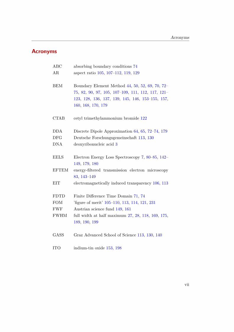
The principle of the plasmon excitation by Otto and Kretschmann is shown in Fig. 2.6and discussed in the caption.
8

2.2. Derivation of surface plasmon polaritons
2.2. Derivation of surface plasmon polaritons
Plasmons are (bosonic) elementary excitations in a metallic5 solid. The questionwhether we should treat them in a quantum mechanical or classical way is discussedin Sec. 3.1.
One of the most simple but nevertheless very utile models to describe the response ofa metallic particle exposed to an electromagnetic field was proposed by Paul Drude6
[37,38] at the beginning of the 20th century and further extended by Hendrik Lorentz7
five years later (consult [39] for a detailed discussion). In 1933 Arnold Sommerfeld8
and Hans Bethe9 expanded the classical Lorentz-Drude model and eliminated someproblems in the description of thermal electrons by accounting for the Pauli principleof quantum mechanics and replacing the Maxwell-Boltzmann with the Fermi-Diracdistribution (again see [39]).
Drude assumed a microscopic description of the electron dynamics in a metal inclassical terms, and obtained the equation of motion of a damped oscillator wherethe electrons are moving between heavier, relatively immobile background ions:
Drude-Sommerfeld model of a free electron gas
me∂2r
∂t2+meγd
∂r
∂t= eE0e
−iωt, (2.1)
where γd describes a phenomenological damping term, me the effective free electronmass, e the free electron charge and ω and E0 are the frequency and amplitude of theapplied electric field respectively. Eq. (2.1) can be solved by the ansatz r(t) = r0e
−iωt
[4] which directly leads to the dielectric function of Drude form5Recently it has been shown [35, 36] that also doped graphene may serve as an unique two-dimensional plasmonic material with certain advantages compared to metals (lower losses andmuch longer plasmon lifetimes).
6Born 12th July 1863 in Braunschweig; † 5th July 1906 in Berlin.7Born 18th July 1853 in Arnheim; † 4th February 1928 in Haarlem.8Born 5th December 1868 in Königsberg; † 26th April 1951 in München.9Born 2th July 1906 in Straßburg; † 6th March 2005 in Ithaca, New York.
9

2. The world of plasmons
Dielectric function of Drude form
εd(ω) = ε∞ −ω2p
ω2 + iγd ω, with ωp =
√4πnee2
me. (2.2)
Here ωp is the volume or bulk plasma frequency (electron density ne = 3/(4πrs3), rsis the electron gas parameter and takes the value 0.16 nm for gold and silver [39])and ε∞ describes the ionic background in the metal. If we neglect γd and ε∞ forthe moment, the Drude dielectric function simplifies to εd = 1 − ωp2/ω2 and we candistinguish two frequency regions: If ω is larger than ωp, εd is positive and thecorresponding refractive index n = √εd is a real quantity10. But if ω is smaller thanωp, εd becomes negative and n is imaginary. An imaginary refractive index impliesthat an electromagnetic wave cannot propagate inside the medium.
The specific value of ωp for most metals lies in the ultraviolet region, which is thereason why they are shiny and glittering in the visible spectrum. A light wave withω < ωp is reflected, because the electrons in the metal screen the light. On the otherhand if ω > ωp the light wave gets transmitted (the metal becomes transparent), sincethe electrons in the metal are too slow and cannot respond fast enough to screen thefield.
This treatment of a free electron gas already gives quite accurate results for theoptical properties of metals in the infrared region, but since higher-energy photonscan also promote bound electrons from lower-lying bands into the conduction band [4](see Fig. 2.1) the Drude model becomes inaccurate for the visible regime as indicatedin Fig. 2.2.
As will be discussed in Sec. 3.1 in more detail, the dielectric function describes theresponse of a material and can either be obtained by first principle calculations or10In general n = ±
√ε and the positive sign is chosen for causality reasons in the system. A negative
refractive index does not occur in nature but can be artificially generated with metamaterials,e.g. see [10–12].
10

2.2. Derivation of surface plasmon polaritons
Figure 2.1.: Electronic band structure of gold, taken from [40]. Above 2 eV (i.e.light wavelengths shorter than 620 nm) electrons can be promoted from the d-bandsbelow the Fermi energy to states above, which leads to strong plasmon dampingand the absorption of bluish light yielding the golden color.
from measurements. In our simulations we will use the dielectric data11 obtainedfrom experiments, but unfortunately there are some difficulties. First the resultsfrom different experiments are not always consistent as shown in Fig. 2.3. Especiallythe data published in [43] shows some additional features compared to [41] for goldand silver around 1 eV (≈ 1240 nm)12, see real part in Fig. 2.3(a) and zig-zag fea-tures in Fig. 2.3(b). Second the dielectric function can be determined from opticalexperiments on bulk solids, thin solid films or clusters [44].
11In the literature most of the time the complex refractive index is tabulated, the connection to thedielectric function is given by ε = ε1 + iε2 = n2 = (n+ ik)2. The real and imaginary parts of εthen follow as ε1 = n2 − k2 and ε2 = 2nk.
12The conversion factor between eV and nm is 1239.84 as discussed in App. A.2.
11

2. The world of plasmons
Figure 2.2.: Real and imaginary parts of the dielectric function for gold (a)-(b)and silver (c)-(d). The experimental data together with the measuring uncertaintyhave been taken from Johnson and Christy [41]. In the inset on the left hand panelswe list the corresponding Drude parameters, see Eq. (2.2). The imaginary part ofthe Drude dielectric function for gold becomes invalid for energies above 1.9 eV,see (b), because at this energy interband transitions set in. The line for the d-band contribution in (b) is obtained from a simple comparison between the Drudedielectric function and the experimental result, also see [42].
2.2.1. Electromagnetic waves at interfaces
In Chap. 3 we will see that the wave equation (3.16) in Helmholtz form is the onerelation to rule them all, electromagnetic fields always have to obey:(
∇2 + εk2)E(r, ω) = 0.
12

2.2. Derivation of surface plasmon polaritons
Figure 2.3.: Comparison of the dielectric data for gold (a) and silver (b) obtainedfrom experiment and published in [41] and [43].
By following [4] let us investigate a planar interface between a metal and a dielectricwith ε1 = εm for the metal at z < 0, and ε2 = εb for the dielectric at z > 0. Thewave equation now has to be solved separately in each region of constant ε and thecorresponding boundary conditions tell us how to match the two solutions at theinterface. In general, Maxwell’s equations allow two sets of self-consistent solutionswith different polarizations – TM (or p-polarized) and TE (or s-polarized) modes.Since we do not get a plasmonic excitation for the latter (see [45] for example), weneglect TE modes and write down the solution of Eq. (3.16) as [4]:
Ej =
Exj0Ezj
eikxx−iωteikzj z, j = 1, 2. (2.3)
The component kx of the wave vector parallel to the interface is conserved, thus theindex j indicating the medium is unnecessary there. The boundary conditions (seeApp. A.1) yield the following relations
Ex1 − Ex2 = 0, (2.4a)
ε1Ez1 − ε2Ez2 = 0, (2.4b)
i.e. the parallel field component is continuous, whereas the perpendicular compo-
13

2. The world of plasmons
nent is discontinuous. To solve (2.4) the corresponding determinant has to vanish.Together with Gauss’ law [Eq. (3.1a)], we obtain the following relations for the wavevector k
k2x + k2
zj = εjk2 = εj
(ω
c
)2−→ kzj =
√εj
(ω
c
)2− k2
x, j = 1, 2. (2.5)
This directly yields the dispersion relation between the wave vector components andthe angular frequency ω
Plasmon dispersion relation
kx = ω
c
(ε1ε2ε1 + ε2
)1/2
, (2.6)
kzj = ω
c
(ε2j
ε1 + ε2
)1/2
, j = 1, 2. (2.7)
We are looking for solutions that are propagating along the surface, i.e. we requirea real kx.
Figure 2.4.: An evanescent wave corresponds to a TM-mode that propagates alongthe interface of a metal and a dielectric, where the z-component of the electric fielddecays exponentially.
14

2.2. Derivation of surface plasmon polaritons
From the dispersion relation it follows that the conditions for the existence of aninterface mode are given by
ε1 ε2 < 0, ε1 + ε2 < 0, (2.8)
which results in an electromagnetic wave bound to the interface13, see Fig. 2.4. Theresulting imaginary kzj corresponds to exponentially decaying (so called evanescent)waves.
Figure 2.5.: Plasmon dispersion relation for a metal/air interface. Since the dis-persion line of plasmons (red line, without damping; blue line for free electrons)does not cross the light cone (yellow line) at any point, it is not possible to excitea surface plasmon at a metal air interface with a light wave. Yet the light cone canbe tilted (dotted yellow line) if we change from free space to a dielectric medium.
The dispersion relation (2.6) is plotted in Fig. 2.5. Since the red line of the surfaceplasmon polariton does not cross the light cone at any point, a direct excitation ofsurface plasmons with an electromagnetic wave is not possible (the momentum oflight is always too small). Nevertheless surface plasmon polaritons can be excited,of course, one just has to provide the missing momentum contribution. This can bedone through a tilt of the light line ω = ckx to ckx/n in a dielectric medium as shownin Fig. 2.5 and Fig. 2.6.
13See [4] or [21] for a more detailed discussion.
15
2. The world of plasmons
Figure 2.6.: Two configurations that provide the missing momentum contributiondiscussed in the text for the excitation of surface plasmons. (a) Otto configura-tion: The total reflection at the prism/air interface generates an evanescent fieldthat excites a SPP at the dielectric/metal interface. This is an useful methodwhen the metal surface should not be damaged, but it is difficult to keep the con-stant distance (usually of the order of λ) between the metal and the prism. (b)Kretschmann configuration: Here the total reflection at the prism/metal interfacegenerates an evanescent field that excites a surface plasmon at the opposite met-al/air interface. The thickness of the metal film must be smaller than the skindepth [see Eq. (2.9)] of the evanescent field.
Skin depth and propagation length
The imaginary part of the dielectric function is related to the energy dissipation ofthe material, i.e. if an electromagnetic waves impinges on a metal surface it can onlypenetrate the solid up to a certain material dependent depth. This so called skindepth ζ is defined as the distance, where the exponentially decreasing evanescent fielde−|kzj ||z| falls to 1/e [21, 44]:
Skin depth
ζi = 1|kzi|
or
ζb = λ
2π
(εm+εbε2b
)1/2
in medium with εb,
ζm = λ2π
(εm+εbε2m
)1/2in metal with εm.
(2.9)
Since the dielectric background constant εb is usually much smaller than the real
16

2.2. Derivation of surface plasmon polaritons
part of εm, inside the metal Eq. (2.9) can be replaced with the approximation ζm ≈λ/(2πε′m), where εm = ε′m + i ε′′m.If a surface plasmon propagates along a smooth surface, its intensity decreases ase−2k′′xx [21], where kx = k′x + i k′′x. The length δ = 1/2k′′x after which the intensity hasfallen to 1/e can be defined as the propagation length.
2.2.2. Particle plasmons
In general, we have seen that plasmons arise from an interplay of electron densityoscillations and the exciting electromagnetic fields. In this sense, we should talkabout surface plasmon polaritons and also distinguish the propagating (evanescent)modes at the interface of a metal and a dielectric from their localized counterpartat the surface of metallic particles (so called particle plasmon polaritons). If anelectromagnetic wave impinges on a metallic nanoparticle (whose spatial dimensionis assumed to be much smaller than the wavelength of light), the electron gas getspolarized (polarization charges at the surface) and the arising restoring force againforms a plasmonic oscillation, see Fig. 2.7.
Figure 2.7.: Excitation of particles plasmons through the polarization of metallicnanoparticles. At the resonance frequency the plasmons are oscillating with a 90°phase difference (180° above resonance). Also a magnetic polarization occurs, butmost of the time it can be neglected for reasons discussed in Sec. 2.5.
The metallic particle thus acts like an oscillator and the corresponding resonance be-havior determines the optical properties [46]. Since we solely discuss particle plasmonpolaritons in this work, we will furthermore always refer to them.
17

2. The world of plasmons
2.3. Tuning the plasmon resonance
When a metallic nanoparticle is illuminated by white light, the plasmonic resonancedetermines the color we observe, see Fig. 2.8. This behavior is nothing new: Mi-croscopic gold and silver particles incorporated in the stained glasses of old churchwindows are responsible for their beautiful lustrous colors14. Another very famousexample dates back to antiquity – a Roman cup made of dichroic glass illustratingthe myth of King Lycurgus15 [49, 50].
Figure 2.8.: Nanoparticles of various shape and size in solution – the plasmonicresonance determines the color.(Photo by Carsten Sönnichsen, http://www.nano-bio-tech.de/).
Let us discuss this topic more precisely: We can tune the resonance of the surfaceplasmon polariton by changing the size or shape of a metallic nanoparticle, as plottedin Fig. 2.9. We recognize that the effect of squeezing a sphere to a rod-like particle hasa much bigger impact than increasing its diameter and the upper panel in Fig. 2.9(b) also shows that the resonance intensity has a maximum for the aspect ratiosomewhere between 0.3 and 0.4.
The plasmonic resonance is not only sensitive to the shape and size of a nanostructure,14The windows of Sainte Chapelle in Paris are a very nice example for this: Light transmission
through the metal ions in the stained glass strongly depends on the incident and viewing an-gles. At sunset, the grazing-angle scattering of light by gold particles in the window creates apronounced red glow that appears to slowly move downward, while intensities of blue tints fromions of copper or cobalt remain the same [47,48].
15Lycurgus cup, 4th century AD, British Museum, London.
18

2.3. Tuning the plasmon resonance
Figure 2.9.: Tuning the resonance of a surface plasmon polariton by changingthe diameter of a gold nanosphere (a) or by squeezing its aspect ratio (b). Theupper panels show the scattering cross section, in the lower panels we report thecorresponding density plots.
also the dielectric medium surrounding the particle plays a key role, see [51] forexample. In Fig. 2.10 the sensitivity of a nanorod to the dielectric background εb isshown.
Even the slightest change in the dielectric surrounding leads to a detectable shift ofthe resonance energy. That is the reason why metallic nanoparticles are very suitablefor sensing applications: Placing a molecule in the vicinity of a nanoparticle effectsthe dielectric environment and therefore shifts the plasmon peak. As already men-tioned in the introduction, bio-sensing is one of the major applications for plasmonicnanoparticles. Thus naturally the question of the optimal shape and size of a sensor
19

2. The world of plasmons
Figure 2.10.: Scattering cross section of a gold nanorod with diameter 10 nm andan arm length of 35 nm. The dielectric constant ε of the embedding medium variesfrom 1.0 to 2.0, the panel on the right again shows the corresponding density plot.
made of nanoparticles arises. A comprehensive analysis of this question can be foundin Chap. 8 and Chap. 9, and we will also briefly highlight the principle of plasmonicsensing in the following subsection.
The influence of the embedding medium on a metallic nanoparticle is a tricky topic asdiscussed in Sec. 4.5.3. For example, if particles in aqueous solution are investigated, aconstant and homogeneous water temperature must be assured because the refractiveindex of water is temperature dependent [52]. Indeed, the change from 20 to40 leads to a resonance shift of about 1 nm [53], which for very accurate sensingapplications may become important – especially when heat is generated through anexciting laser field [54].
2.3.1. Principle of plasmonic (bio-)sensing
One possible route to plasmonic molecular sensors is given by exploiting the enhance-ment of the decay rates of fluorophores in the vicinity of MNPs [55,56]. The moleculeuses the nanoparticle as an antenna in order to emit its energy much faster – theenhancement can be two orders of magnitude and more. In Fig. 2.11 an example pub-lished in [55] is shown, where fluorophores were deposited onto two different samples
20

2.3. Tuning the plasmon resonance
of nanodisk-arrays. The molecules absorb in the ultraviolet and emit in the visibleregime, which allows a separation of the excitation and emission channel.
Figure 2.11.: Figure taken from [55]. (a) Electron-microscopic image of two differ-ent quadratic arrays of gold nanodisk samples on a silicon dioxide substrate, onegeometry is chosen resonant and the other off-resonant to the fluorophore emission.The size parameters and mutual distances are shown in the lower panel. The largeinterparticle distance of ~ 50 nm ensures that coupling effects between the diskscan be neglected. (b) Absorbance spectra (dashed and dotted line) of the twonanodisk samples as well as the emission spectrum (solid line, maximum at 612nm) of the fluorophores.
If the plasmon frequency of the disk-arrays is in resonance with the molecular emis-sion (blue dashed line in Fig. 2.11), each disk acts as a supplemental antenna for themolecules. The nonradiative near-field of the fluorophores gets converted into radi-ating far-field, which leads to the dramatic increase of the radiative decay rate [55].as shown in Fig. 2.12.
The decay rate of the molecule can be calculated by Fermi’s golden rule, as has beenshown in [56]. In the cited work the decay rate of the coupled MNP-fluorophoresystem is derived, which is fully determined by the dyadic Green function of classicalelectrodynamics. It can be described in terms of a self-interaction, where the molec-ular dipole polarizes the MNP, and the total electric field acts, in turn, back on thedipole [see Fig. 2.13(b)].
But not only the radiative decay rate gets enhanced, also the nonradiative decaychannel is strongly increased because of Ohmic power loss inside the nanodisks asindicated in Fig. 2.13 and discussed in [55].
21

2. The world of plasmons
Figure 2.12.: Figure taken from [55]. Panel (a) shows the fitted fluorescencecurves for the two samples of Fig. 2.11 (dashed and dotted lines), for a flat goldfilm (yellow line in lower left corner), and for the bare silicon substrate (black solidline). (b) Fluorescence intensity results of simulations with the boundary elementmethod (see 4.3) for the corresponding setup, for further details see [55].
Figure 2.13.: Energy levels, radiative (Γrad) and non-radiative (Γmol) decay ratesof a free molecule (a) and a molecule coupled to a metallic nanoparticle (b). Thedecay rates for the free fluorophore are indicated with a 0 in the superscript and theexcitation is noted as Γext. The plasmon resonance tuned to the molecular emissionenhances both, the radiative as well as the nonradiative decay channel [55].
This example illustrated the cumulative effect of many molecules spread over an arrayof nanoparticles, but the crux of the whole sensing problem is given by the possibilityto detect one single molecule. Here once again the near-field enhancement of metallicnanoparticles is of great importance. In Fig. 2.14 the near-field enhancement of abowtie nanoantenna is plotted on a logarithmic scale.
22

2.3. Tuning the plasmon resonance
Figure 2.14.: (a) Real part of electric field (in the gap region the field is about7 times larger than the background) and normalized surface charge, each one atthe resonance energy for the gold bowtie nanoantenna with 5 nm gap distance.(b) Near-field enhancement |E|2/|E0|2 calculated for the same nanoentenna. Thetriangle size is 45 nm in x, 40 nm in y and 8 nm in z direction.
For a gap distance of 5 nm we get a strong intensity enhancement as well as alocalization in the gap region. Placing a single molecule in the hot spot at thegap leads the way to single molecule sensors, see Fig. 7.4. In [57], for example,single molecule fluorescence enhancements up to a factor of 1340 for gold bowtienanoantennas have been reported.
23

2. The world of plasmons
A nice review about advances in the field of optical-biosensors can be foundin [58]. A typical example of the working principle of a sensor based on surfaceplasmons is shown in Fig. 2.15 below, where the binding of analytes can bemeasured non-invasively in real time.
Figure 2.15.: The changes in the refractive index in the immediate vicinity ofa surface layer are detected with a sensor chip. The plasmonic resonance isobserved as a sharp shadow in the reflected light at an angle that depends onthe mass of material at the surface – this angle shifts if biomolecules bind tothe surface. (Figure and caption adopted from [58].)
Additional remark
24
2.3. Tuning the plasmon resonance
2.3.2. Light absorption in solar cells
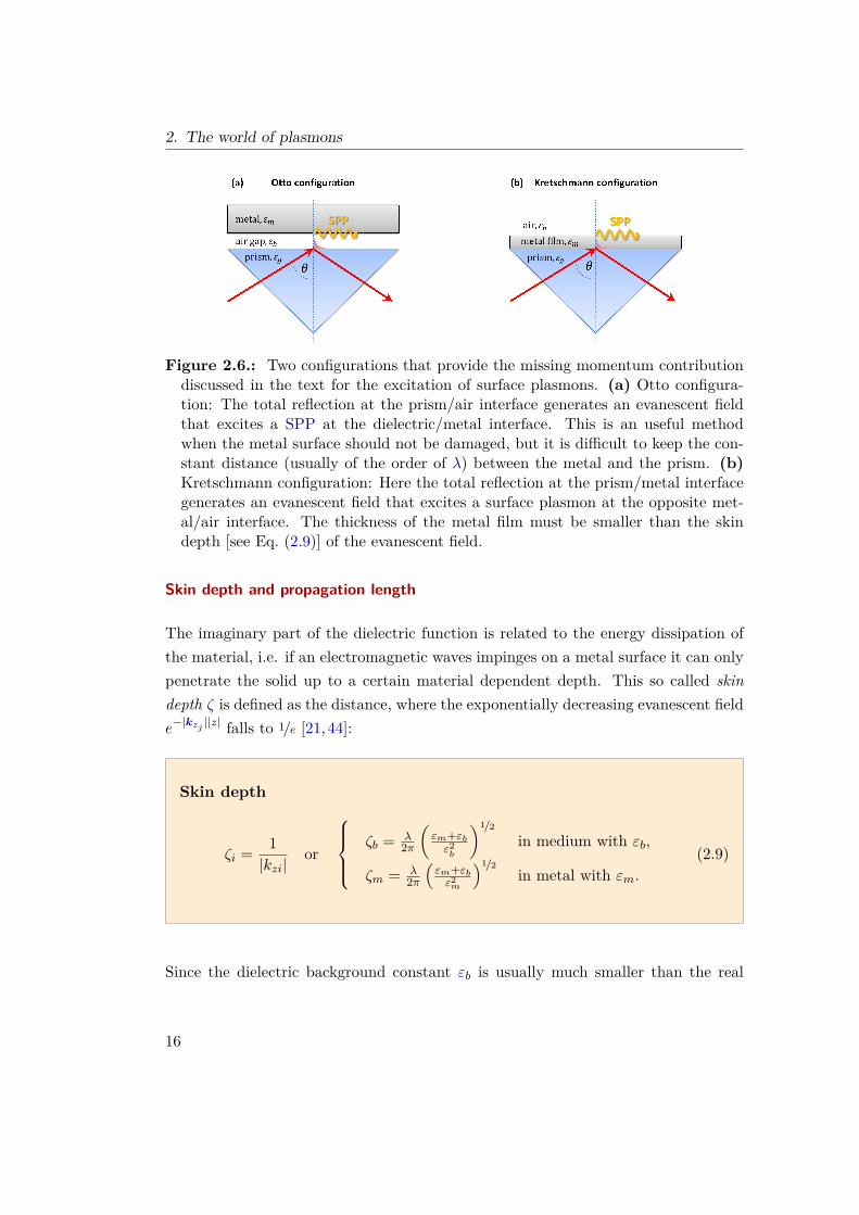
Another of the many possible applications that could be revolutionized (or at leastvery much improved) by plasmonic structures are photovoltaic devices [20, 59]. Thecombination of MNPs and semiconductor materials, for example, allows a consider-able reduction in the physical thickness of absorber layers, and yields new possibilitiesfor the design of solar-cells. We don’t want to go into the details of this broad re-search field, but since some of the solar cell aspects are again nice examples for thetunability of the plasmonic resonance we will shortly dwell upon this subject. Areview about recent advances at the intersection of plasmonics and photovoltaicscan be found in [59] and a brief overview of three different light-trapping thin-filmgeometries is depicted in Fig. 2.16.
Figure 2.16.: Three different plasmonic geometries for light-trapping for thin-filmsolar cells, figure and caption taken from [59]. (a)Metallic nanoparticles embeddedat the solar cell surface scatter light preferentially into the semiconductor thin filmwhich leads to an increase of the optical path length in the cell. (b) If the particlesare embedded in the semiconductor, the creation of electron-hole pairs is causedby the particle’s near-field. (c) Light coupling through a corrugated metal backsurface.
Unfortunately for the developing of photovoltaic cells our sun is an incoherent blackbody source and has nothing to do with the compliant light of a laser. An efficientsolar device must therefore have a very broad absorption spectrum for all parts ofsun light. There are two easy ways to broaden the absorption of a MNP, either byadding an additional coating around the structure or simply by coupling it to anotherparticle, see Fig. 2.17.
25

2. The world of plasmons
Figure 2.17: The blue dottedline shows the normalized ab-sorption spectrum for a 10nm gold sphere. Adding anadditional layer around thesphere (see inset, nlayer =10), yields the broadened redabsorption line (again nor-malized to 1). The light colorrange was approximated ac-cording to Fig. A.2.
The coupling of two or more metallic nanoparticles leads to a hybridization ofthe energy levels. Fig. 2.18 shows the example for spherical dimers.
Figure 2.18.: Energy levels of two coupled spherical nanoparticles (see [60,61]),note the occurrence of bonding and antibonding modes.
Additional remark
26

2.4. Damping mechanisms of surface plasmon polaritons
2.4. Damping mechanisms of surface plasmon polaritons
As discussed at the beginning of this chapter, a plasmon is formed when a coherentcharge density oscillation is induced in the electron gas of a metallic nanoparticle byan external excitation. This collective motion of the electrons can easily be disturbed,for example by scattering events that destroy the phase coherence. One can imaginethis dephasing by simply kicking an electron out of the lock-step march, due toscattering with impurities, phonons, other electrons, and so on. The electron stillhas its kinetic energy but the phase coherence gets destroyed. Fig. 2.19 gives anoverview about the different decay channels and in Fig. 2.20 the corresponding timescales are plotted.
Figure 2.19.: Usually a particle plasmon shares the destiny of a mayfly, albeit ona different time scale: After a quite short existence it is doomed to decay. It caneither decay radiatively (left) and emit photons or lose its energy non radiativelyvia intra- and interband transitions (right), also see Fig. 2.20. Both decay channelscontribute to the homogeneous linewidth Γ.
The radiative and nonradiative break up and decay processes of plasmons result inhighly excited electron-hole pairs, which thermalize by further collision processes ona sub-ps time scale [62, 63] to a distribution of “hot” electrons16 and holes [46].
The decay time τ of a particle plasmon oscillation can be determined from the ho-mogeneous linewidth Γ of the spectral resonance of a plasmon, see App. A.3. Γ isdefined as the full width at half maximum (FWHM) and is inversely proportional to16Since the heat capacity of the electronic system is much smaller than that of the ion lattice, an
excitation by femtosecond laser pulses can generate extremely high electron temperatures [46].
27

2. The world of plasmons
Figure 2.20.: List of typical plasmon decay times obtained from [46]. After about10 fs the particle plasmon decomposes into electron-hole pairs, which further ther-malize on a sub-ps timescale to a distribution of hot electrons and holes. Finallythrough electron-phonon coupling the energy is transfered to the lattice as heat.
the decay time τ : Γ ∝ τ−1, see Eq. (A.15). Fig. 2.21 shows an example for a nanorodantenna, also see Fig. 13.1.
Figure 2.21.: Homogeneous linewidth (FWHM) Γ and plasmon decay time τ fora gold nanorod antenna (rod length 280 nm, width 60 nm, height 40 nm, and gapdistance 65 nm). The resulting decay time τ ≈ 5.5 fs for this geometry has alsobeen verified by autocorrelation measurements, see Chap. 13.
Increased damping, for example caused by defects in the nanoparticles’ crystal struc-ture, thus leads to a broadening of the spectral linewidth. Note that Γ can vary morethan a factor of ten for different nanoparticle geometries – defining the quality of aplasmonic sensor simply over the shift of the resonance may therefore be a little bitsimplistic. In Chap. 8 we will introduce several ’figures of merit’ to allow a betterquality comparison of different plasmonic sensors.
28

2.5. Magnetic effects
As discussed in Chap. 7, for the direct measurement of the temporal evolution ofparticle plasmons ultrashort laser pulses are necessary. These pulses have becomeavailable in the past decade and thus probing ultrafast plasmon dynamics directly inthe time domain with fs time-resolution has become possible, see Chap. 13.
2.5. Magnetic effects
A light wave always consists of an oscillating electric and magnetic field, the onenever occurring without the other. But since at optical frequencies the value ofthe magnetic permeability µ = (1 + 4πχm) ≈ 1, the magnetic component of lightgenerally plays an insignificant role and can often be neglected. This aspect can beeasily understood in a simplified picture with the Lorentz force FL [64–66]. As wehave highlighted above, the electron cloud of a metallic nanoparticle can interact withan impinging light wave. In classical electrodynamics the effect of the electromagneticfield on a moving charge q is described through [66]
Lorentz force in Gaussian units
FL = q
[E +
(v
c×B
)]. (2.10)
The ratio of the velocity |v| to the speed of light c determines the ratio of the magneticcontribution to it’s electric counterpart [65]. The norm of the charge velocity in solidstate physics is roughly given by the Fermi velocity17 vF which implies for the ratiothat vF/c ≈ 1/300 [65]. The magnetic response of a material is determined by themagnetic susceptibility χm, which scales as (vF/c)2. Thus it follows that the magneticresponse is four orders of magnitude weaker than the ease with which the samematerial is polarized [64].17Numerical value for gold and silver particles vF ≈ 1.4 nm/fs, Fermi energy EF ≈ 5.53 eV respectively
[39].
29
2. The world of plasmons
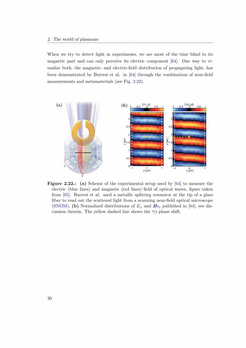
When we try to detect light in experiments, we are most of the time blind to itsmagnetic part and can only perceive its electric component [64]. One way to vi-sualize both, the magnetic- and electric-field distribution of propagating light, hasbeen demonstrated by Burresi et al. in [64] through the combination of near-fieldmeasurements and metamaterials (see Fig. 2.22).
Figure 2.22.: (a) Scheme of the experimental setup used by [64] to measure theelectric (blue lines) and magnetic (red lines) field of optical waves, figure takenfrom [65]. Burresi et al. used a metallic splitring resonator at the tip of a glassfiber to read out the scattered light from a scanning near-field optical microscope(SNOM). (b) Normalized distributions of Ex and Bsz published in [64], see dis-cussion therein. The yellow dashed line shows the π/2 phase shift.
30

3. Theory
The unification of the theories describing electric and magnetic aspects of our worldwas one of the great scientific achievements in the 19th century [67] and broughtus a very successful part of theoretical physics: classical field theory. A detailedoverview about the historical evolution from René Descartes up to Maxwell andLorentz can be found in the excellent book of Whittaker [68]. After the revolutionof our understanding of the basic forces and constituents of matter in the last 100years, classical electrodynamics found its place in a sector of the unified descriptionof particles and interactions known as the standard model [66].
3.1. Quantum versus classical field theory
Atoms and their corresponding electromagnetic fields fluctuate quite rapidly on thenanoscale, so usually we need to average over a larger region to obtain a macroscopictheory. In this sense the concept of the ordinary electromagnetic fields is a classicalnotion. It can be thought of as the classical limit (limit of large photon numbers andsmall momentum and energy transfers) of quantum electrodynamics (QED)1 [66].But nanoparticles are situated in the gray zone between the micro- and macrocosm– they are very small compared to classical objects but they still consist of severalthousands to millions of atoms. Nevertheless surface plasmons are bosonic quasi-particles and have a true quantum nature that has been demonstrated by tunnelingexperiments for example, see [70]. Hence, for the theoretical description we can eithercome from the bottom and try to apply a quantum mechanical treatment or we candeal with plasmonic structures in terms of classical field theory (and hope that theparticles are not too small).
1A nice introduction into the topic of QED can be found in [69] for example.
31

3. Theory
At which point is it justified, that we neglect (or at least gloss over) the discretephoton aspect of the electromagnetic field and change from QED to Maxwell’s theory?In the domain of macroscopic phenomena virtually always, as the examples discussedin [66] elucidate: The root mean square electric field one meter away from a 100 wattlight bulb is of the order of 50 V/m and there are of the order of 1015 visible photonsper cm2 per second. Similarly, an antenna that emits isotropically with a powerof 100 watts at 108 Hz produces a root mean square electric field of only 0.5 mV/m
at a distance of 100 kilometers, but this still corresponds to a flux of 1012 photonsper cm2 per second. Ordinarily an apparatus will not be sensitive to the individualphotons; the cumulative effect of many photons emitted or absorbed will appearas a continuous, macroscopically observable response. Then a completely classicaldescription in terms of the Maxwell equations is permitted and is appropriate.
A rough estimate for the justification of a classical treatment is given by a highnumber of involved photons where at the same time their momentum has to be smallcompared to the material system2. This is true for metallic nanoparticles and in linearresponse, one can employ the fluctuation-dissipation theorem to relate the dielectricresponse to the dyadic Green tensor of Maxwell’s theory where all the details of themetal dynamics are embodied in the dielectric function. This is exactly what weare going to do, we will hide the quantum-mechanical properties of matter in theirdielectric description which is obtained by experiment (see Fig. 2.2 and [41]). In thisway, we are communicating with the microscopic world via ε and µ.
Nevertheless, the whole concept of a dielectric function becomes questionable if theinvestigated nanoparticles are too small (caution for structures below 5 nm may bejustified). Also if coupled particles get very close to each other, the onset of screeningeffects and electron tunneling across the gap region significantly modifies the opticalresponse as reported in [72]. In the cited work, the authors present a fully quantummechanical description of nanoparticle dimers in terms of time-dependent densityfunctional theory and state that quantum effects for dimers become important fordimer separations below 1 nm.
2Because of energy and momentum conservation at least the time averaged electromagnetic field canstill be treated in a classical way, also for clearly quantum mechanical processes like spontaneousemission [66]. A nice discussion of this topic is also given in the introductory chapters of [71]
32

3.2. Maxwell’s theory of electromagnetism
3.2. Maxwell’s theory of electromagnetism
We treat the electromagnetic fields as three-dimensional vector fields. Such fieldsare fully determined by their divergence and curl – that explains the structure andappearance of their mathematical description: Maxwell’s equations. In Gaussianunits and in their macroscopic version they read as [66]
Macroscopic Maxwell equations in atomic units
∇ ·D(r, t) = 4π%(r, t), (Gauss’s Law) (3.1a)
∇ ·B(r, t) = 0, (magnetic analogon) (3.1b)
∇×H(r, t) = 4πcj + 1
c
∂D(r, t)∂t
, (Ampère’s Circuital Law) (3.1c)
∇×E(r, t) = −1c
∂B(r, t)∂t
. (Faraday’s Induction Law) (3.1d)
Here B = µH is the magnetic field (magnetic permeability µ = 1 throughout, seeSec. 2.5), D = εE is the dielectric displacement3, % the free charge density, c thespeed of light, and j the current density.
Maxwell’s equations are partial differential equations of first order. In many casesthey are linear4 in the fields E and B. Because of this linearity it is sufficient toonly investigate time harmonic fields, any complex solution of the system can thenbe described as a superposition of them. Henceforth we will use
E(r, t) = E(r)e−iωt, B(r, t) = B(r)e−iωt. (3.2)
3This relation connects the microscopic response with a macroscopic field, a more detailed discussionfollows in Sec. 3.2.1.
4Nonlinear effects may arise at interaction with fiber glass or certain magnetic materials and manyother systems.
33

3. Theory
The inverse square law of the electrostatic force was shown quantitatively inexperiments by Coulomb5 and Cavendish6 [66]. Applying the divergence theoremtogether with Gauss’s law allows the derivation of the first of Maxwell’s equations,Eq. (3.1a). But Coulomb’s inverse square law also leads to another remarkablycondition: The photon has to be a massless particle [66]! We can verify thishypothesis solely with experiments, and Maxwell’s equations are based on thisassumption. The consequences of a massive photon are once again discussedin [66], for example, and the experimental verification of Coulomb’s law alreadygives a very good upper limit for the photon mass mγ , see [73]. Very accurateresults for mγ can be obtained by measuring the magnetic field of earth, viz.
mγ < 4× 10−51 kg, (3.3)
or the cosmic magnetic vector potential, see [74]. Also the Schumann resonances(stationary electromagnetic waves along the circumference of the earth) allow fora very simple but surprisingly accurate estimation of the upper limit of mγ .
Additional remark
If no sources are present (% = 0, j = 0) Maxwell’s equations reduce to
Maxwell’s equations in vacuum
∇ ·E = 0, ∇×B − 1c
∂E
∂t= 0, (3.4a)
∇ ·B = 0, ∇×E + 1c
∂B
∂t= 0. (3.4b)
5Born 14th June 1736 in Angoulême; † 23th August 1806 in Paris.6Born 10th October 1731 in Nice; † 24th February 1810 in London.
34

3.2. Maxwell’s theory of electromagnetism
3.2.1. Linear and nonlinear optical response
If we apply an external electric field to a polarizable (dielectric) medium, the elec-trons in the material response with a microscopic shift but still remain bound totheir associated atoms. The cumulative effect of all displaced electrons results in amacroscopic polarization of the material that can be described by a net charge dis-tribution. In terms of Maxwell’s theory it becomes useful if we distinguish betweenthis bound charge distribution and that of free charges, which we have introducedas % in Eq. (3.1a). The contribution of the bound charges is incorporated elsewhere,but let us discuss this in more detail. The electromagnetic fields obey the followingrelations
D = E + 4πP , B = H + 4πM , (3.5)
where P is the dipole moment per unit volume andM refers to the magnetic momentper unit volume. Since we focus our attention only to nonmagnetic media, we canset M ≡ 0 (see Sec. 2.5) and combine Maxwell’s equations to
∇2E −∇(∇ ·E)− 1c2∂2E
∂t2− 4π∂2P
c2∂t2= 0. (3.6)
In principle, one now requires a full microscopic theory of the response of a particularmaterial to relate the macroscopic electric field E to the polarization P [66, 75].Making some assumptions about the relationship between P and E will make ourlives much more easy.
The change in electrostatic potential over distances of the order of an angstrom canbe several electron volts. In this sense, an electron bound to an atom or molecule,or moving through a solid or dense liquid, experiences electric fields of the order of109 V/cm [75]. The laboratory fields of interest are then small compared to the electricfields experienced by the electrons in the atoms and molecules of the investigatedmatter. In this circumstance, we can expand P (r, t) in a Taylor series in powers of themacroscopic field7 E(r, t). The αth Cartesian component of the dipole moment perunit volume is a function of the three Cartesian components of the electric field Eβ =
7Another method sometimes discussed in literature models the atomic or molecular structure ex-plicitly. There one relates the dipole moment per unit volume to that of an atomic or molecularconstituent and writes this as a Taylor series similar to our approach, see [75, 76] and referencestherein.
35

3. Theory
Eβ(r, t), with β ∈ x, y, z; therefore we can write the Taylor series as follows:
Pα(r, t) = P (0)α +
∑β
(∂Pα∂Eβ
)0Eβ + 1
2!∑βγ
(∂2Pα
∂Eβ∂Eγ
)0EβEγ+
+ 13!∑βγδ
(∂3Pα
∂Eβ∂Eγ∂Eδ
)0EβEγEδ + · · · .
Here we have assumed that the dipole moment P (r, t) depends on the electric fieldE at the same point r in space and the same time t, which is not really a realisticassumption – we will introduce a more proper treatment in the next section andwe will see, that we can incorporate certain nonlocal aspects in the susceptibilitytensor.
In this work, we are interested in dielectric materials within which any dipole momentis induced by the external field. Therefore the electric dipole moment per unit volumeat zero field, P (0)
α , vanishes8, and we will henceforth write
Pα(r, t) =∑β
χ(1)αβEβ +
∑βγ
χ(2)αβγEβEγ +
∑βγδ
χ(3)αβγδEβEγEδ + · · · , (3.7)
where the susceptibilities χ(i) are tensors of (i+ 1)th rank. χ(1) is the ordinary sus-ceptibility of dielectric theory (usually a diagonal matrix) and χ(2), χ(3) are referredto as the second and third order susceptibilities, respectively. Now we can decomposethe dipole moment into a part which is linear in the electric field, and one part whichis nonlinear:
Pα(r, t) = P (L)α (r, t) + P (NL)
α (r, t), (3.8)
where
8The electrical analogs of ferromagnets, which possess a spontaneous magnetization per unit vol-ume, are the so called ferroelectrics. In these materials the dipole moment P (0) in the absenceof an electric field is nonzero and leads to the presence of a static, macroscopic electric field,E(0)(r). Such time independent effects may be analyzed by the methods of electrostatics andcan be accounted for by including an effective charge density %p = −∇ · P (0), for example.
36

3.2. Maxwell’s theory of electromagnetism
Linear and nonlinear dipole moment per unit volume
P (L)α (r, t) =
∑β
χ(1)αβEβ, (3.9a)
P (NL)α (r, t) =
∑βγ
χ(2)αβγEβEγ +
∑βγδ
χ(3)αβγδEβEγEδ + · · · . (3.9b)
With the electric susceptibility χe (simplified symbol instead of χ(1)) we now obtainthe previously discussed relation, where the microscopic response is incorporated inthe dielectric function:
D = E + 4πP = (1 + 4π χe)E = εE. (3.10)
Furthermore we now have a clear distinction between linear and nonlinear optics:If we insert P (L)
α (r, t) into Maxwell’s equations we obtain a description of electro-magnetic wave propagation in (possibly crystalline) media, described by an electricsusceptibility tensor χαβ, in linear response. All nonlinear effects are part of thehigher order susceptibilities.
Since P and E are vectors, and thus are odd under inversion symmetry, χ(2) mustvanish in any material that is left invariant in form under inversion9. But if the sym-metry is broken (at the interface from one medium to another, for example) or in thecase of surface imperfections [77], we also get χ(2) contributions for centrosymmetricmaterials like gold or silver, see Sec. 7 and [78].
3.2.2. Nonlocal in space and time
The macroscopic field E(r, t) acts as a driving field that leads to a rearrangement ofthe electrons and nuclei in the material. The result is the induced dipole moment P ,
9This is the case for metals like Au or Ag, for the semiconductors Si and Ge as well as for liquids,gases, and for a number of other common crystals. The interested reader may find a very usefulcompilation of the nonzero elements of χ(2) and χ(3) for crystals of various symmetry in [76].
37

3. Theory
which of course will not be built up instantaneously, but is instead the consequenceof the response of the system over some characteristic time interval t − t′ > 0 in therecent past. If, on the other hand, we consider an incident electric field well localizedin space, it will lead to an electronic rearrangement in a certain small region of thematerial. Because of the interaction with neighboring constituents, the material getspolarized in the vicinity of the excitation as well. It follows then that the dipolemoment P (r, t) depends not only on the field at time t and position r, but must bewritten as a convolution in space and time (exemplified only for linear response)
P (L)α (r, t) =
∑β
∫R3⊗R
d3r′dt′ χ(1)αβ(r − r′, t− t′)Eβ(r′, t′). (3.11)
If there are no variations in density or composition, the medium can be treated ashomogeneous in nature. Then the susceptibility tensor χ will not depend on r orr′ separately but only on the spatial difference r − r′. A second simplification canbe exploited. If the electric field exhibits only a slow variation in space and timewe may use E(r′,t′) ≈ E(r,t) and recover Eq. (3.9a), where we now have shown thestructure of the susceptibility tensor in more detail:
P (L)α (r, t) =
∑β
χ(1)αβ(r, t)Eβ(r, t), with χ
(1)αβ(r, t) =
∫d3r′dt′ χαβ(r−r′, t−t′).
(3.12)
The physical meaning of nonlinear response of a material becomes clear if analyzedin Fourier space. Therefore we will briefly list the basic Fourier decompositions,again exemplified for linear response. For simplicity we will use the same symbolsfor functions in Fourier as well as in real space and follow the notation in [75]. TheFourier transform operator and its inverse are denoted by the symbols F and F−1,respectively.
Eβ(k, ω) = F [Eβ(k, ω)] ≡∫d3rdtEβ(r, t)e−ik·reiωt (3.13a)
Eβ(r, t) = F−1[Eβ(k, ω)] ≡∫d3kdω
(2π)4 Eβ(k, ω)eik·re−iωt. (3.13b)
38

3.2. Maxwell’s theory of electromagnetism
With these definitions the transformation for P (L)α follows directly from Eq. (3.11):
P (L)α (r, t) =
∫d3kdω
(2π)4 P(L)α (k, ω)eik·re−iωt, (3.14)
where
P (L)α (k, ω) =
∑β
χ(1)αβ(k, ω)Eβ(k, ω), and χ
(1)αβ(k, ω) =
∫d3rdt χ
(1)αβ(r, t)e−ik·reiωt.
For the rest of this chapter we will stick to the linear response and assume the simplelinear proportionality between P and E. Nonlinear optical responses will again bediscussed in Chap. 7.
3.2.3. Electromagnetic potentials
We now return to Maxwell’s equations. Let us recall their appearance in a sourcefree frequency space:
∇ ·D(r, ω) = 0, ∇×B(r, ω) + i ωD(r, ω) = 0, (3.15a)
∇ ·B(r, ω) = 0, ∇×E(r, ω)− i ωB(r, ω) = 0. (3.15b)
Taking the curl on Ampère’s and Faraday’s law respectively and substituting thecorresponding equations leads us to the wave equation of Helmholtz form:
Wave equation for electromagnetic fields(∇2 + ε
ω2
c2
)E(r, ω)B(r, ω)
= 0. (3.16)
39

3. Theory
This equation is a central result of Maxwell’s theory, since it postulates the existenceof electromagnetic waves. Thus as a possible solution we can write down a planewave propagating in er-direction: eik·r−i ωt, with k = k ek.
If we change from first to second order equations, we can combine the four coupledexpressions of Eq. (3.15) into two new equations and introduce the vector potentialA and the scalar potential Φ. The fields can then be expressed as
Electromagnetic fields expressed with potentials
B = ∇×A, (3.17a)
E = −∇Φ + ikA . (3.17b)
The differential equations for A and Φ still form a coupled system. But because ofthe gauge invariance of the potentials we can choose A and Φ in such a way thatthey fulfill the Lorenz condition [79]
∇ ·A− ikεΦ = 0. (3.18)
This condition does not entirely fix the gauge, but it is coordinate independent(and therefore naturally fits into special relativity) and leads to two decoupled waveequations for A and Φ that are completely equivalent to Maxwell’s equations (3.1):
Helmholtz equation for potentials
∇2Φ + k2εΦ = −4π%, (3.19a)
∇2A+ k2εA = −4πcj . (3.19b)
40

3.2. Maxwell’s theory of electromagnetism
Here we again included external charges and currents as in (3.1).
Maxwell’s equations interweave space and time, electric and magnetic fields insuch a wonderful way, that made Boltzmann express his deepest admiration [67].Throughout time the equations changed their appearance and hence are a niceexample for the mathematical beauty and the huge amount of physics that canbe contained in one single line (constants set to 1, table adopted from [67]):
Homogeneous equations Inhomogeneous equations
Original form:
∂Bx∂x
+ ∂By∂y
+ ∂Bz∂z
= 0, ∂Ex∂x
+ ∂Ey∂y
+ ∂Ez∂z
= %,
∂Ez∂y− ∂Ey
∂z= −∂Bx
∂t
∂Bz∂y− ∂By
∂z= jx + ∂Ex
∂t
∂Ex∂z− ∂Ez
∂x= −∂By
∂t
∂Bx∂z− ∂Bz
∂x= jy + ∂Ey
∂t∂Ey∂x− ∂Ex
∂y= −∂Bz
∂t
∂By∂x− ∂Bx
∂y= jz + ∂Ez
∂t
End of 19th century:
divB = 0 divE = %
rotE = −B rotB = j + E
Beginning of 20th century:
∗ F βα,α = 0 F βα,α = jβ
Mid of 20th century:
dF = 0 δF = J
Additional remark
41

3. Theory
3.3. Rayleigh scattering - The quasistatic approximation
Before we discuss the solution of the full wave equations in the next section, let uselucidate the main idea for a more simplified case. In the limit of small particles(compared to the wavelength λ) we can put k ≈ 0 and neglect all retardation effects.The wave equation (3.19a) for the scalar potential Φ and a non vanishing externalcharge distribution % transforms to the Poisson equation
∇2Φ(r) = −4π%(r) (3.20)
If there are again no external charges present, this equation reduces to the Laplaceequation
∇2Φ(r) = 0 . (3.21)
Because of an almost 200 years old work [80] from the extraordinary autodidactGeorge Green10, we know that we can solve this kind of differential equations withthe introduction of the Green function G
∇2G(r − r′) = −4πδ(r − r′) . (3.22)
With the Dirac delta distribution on the right hand side, we already get a first hintabout the singularity of G. In the quasistatic regime the solution of Eq. (3.22) is
Quasistatic Green function
G(r − r′) = 1|r − r′|
= G(r, r′) (3.23)
plus an arbitrary function which has to obey the Laplace equation [66]. With thisstatic Green function G we are now prepared to solve the Poisson equation within an10Born 14th July 1793 in Sneinton, Nottingham; † 31st May 1841 in Nottingham. See e.g. [81] for
more details on his life.
42

3.3. Rayleigh scattering - The quasistatic approximation
unbounded region, simply by applying Green’s theorem together with appropriateDirichlet or Neumann boundary conditions, see [66] for more details.
Let us assume a given external excitation φext, which, for example, corresponds toplane waves impinging on a nanoparticle. The only possible sources are bound to thenanoparticle surface ∂Ω, therefore the scalar potential can be expressed as [82,83]
φ(r) =∫∂ΩG(r − s′)σ(s′)da′ + φext(r), (3.24)
with σ being the surface charge distribution situated at the interface ∂Ω between thetwo media. Note that this equation fulfills the Poisson equation everywhere exceptat the boundaries.
We make an important step here, that highlights the main idea of our approach inthe quasistatic regime: For an unbounded region we can write down the solutions ofthe Poisson or Laplace equation quite easily. For a bounded region the correspondingboundary conditions come into play and we add artificially a surface charge distri-bution that will be chosen such that the boundary constraints are fulfilled.
The electromagnetic boundary conditions are discussed in App. A.1: The tangentialelectric field and the normal component of the dielectric displacement have to becontinuous at the boundary between two media. The first constraint implies that thescalar potential is continuous Φ1|surf = Φ2|surf, which is guaranteed when the surfacecharge distribution is the same on each side of the boundary: σ1 = σ2.
For the second constraint we have to evaluate the surface derivative of Φ
limr→s
n ·∇Φ(r) ≡ limr→s
∂Φ(r)∂n
= limr→s
∂
∂n
∫∂ΩG(r − s′)σ(s′)da′ + ∂φext(r)
∂n
.
Because of the singularity of G we have to be careful about the limit r → s in theintegral. Let us consider
limr→s
n ·∇∫G(r, s′)σ(s′) da′ (3.25)
43

3. Theory
for a coordinate system where n = ez, r = (0, 0, z)T , and s′ = ρ(cos ϕ, sin ϕ, 0)T isgiven in polar coordinates ρ and ϕ, see [56]. We compute the boundary integral withina small circle with radius R, within which the surface charge σ can be approximatedby a constant. The integral then becomes
limz→±0
n ·∫
r − s′
|r − s′|3da′ → lim
z→±02πz
∫ R
0ρdρ (ρ2 + z2)−
32 = ±2π . (3.26)
The positive or negative sign depends on the direction from where we approachthe surface, whether from inside or outside of the particle boundary (i.e. positivesign inside the particle, negative sign outside of it). With the abbreviation F ( s,s′) = (n·∇)G(s, s′) we finally obtain
limr→s
(n · ∇)Φ(r) = ∂Φ(s)∂n
=∫∂ΩF (s, s′)σ(s′) da′ ± 2πσ(s) + ∂Φext(s)
∂n. (3.27)
3.3.1. From boundary integrals to boundary elements
The calculation of an analytical solution of Eq. (3.27) is only possible for very re-stricted geometries, for example if ∂Ω is a sphere boundary. In Chap. 4 differentnumerical methods and approaches will be discussed, to get solutions for more gen-eral shapes of ∂Ω. The method that has been used throughout this work is theso called Boundary Element Method (BEM). In this approach one approximates thesurface charge as a discrete number of points located at the centroids of small surfaceelements (see Sec. 4.3 for details). Eq. (3.27) then becomes
(∂Φ∂n
)i
=∑j
Fijσj ± 2πσi +(∂Φext∂n
)i, (3.28)
or in a compact matrix notation
44

3.3. Rayleigh scattering - The quasistatic approximation
∂Φ∂n
= Fσ ± 2πσ + ∂Φext∂n
, (3.29)
where F is the matrix with elements F (si, sj).
So far so good, but we still have to account for Maxwell’s boundary conditions. Thecontinuity of the normal component of the dielectric displacement leads to
ε2
(Fσ + 2πσ + ∂Φext
∂n
)= ε1
(Fσ − 2πσ + ∂Φext
∂n
)2πσ(ε2 + ε1) + Fσ(ε2 − ε1) = −(ε2 − ε1)∂Φext
∂n,
where ε1,2 is the (frequency dependent) dielectric function of the correspondingmedium, see Fig. 2.2. From the last expression it follows that
σ = −
2πε2 + ε1ε2 − ε1
1 + F−1 ∂Φext
∂n. (3.30)
With the abbreviation Λ= 2π ε2+ε1ε2−ε11 we get our final result
Quasistatic surface charge
σ = −(Λ + F
)−1 ∂Φext∂n
. (3.31)
Note the elegance of this expression, where material parameters (incorporated by thefrequency dependent Λ) and structural properties (established by F ) of the problemare fully decoupled.
3.3.2. Eigenmode expansion
To compute the surface charge σ according to Eq. (3.31) we have to perform a matrixinversion. The size of the matrix (i.e. the refinement of our surface discretization)
45

3. Theory
is the limiting parameter for the needed computation time (see Sec. C.1). In thequasistatic regime we can significantly speed up the simulation if we expand Eq. (3.31)to plasmon eigenmodes and reduce the inversion of the fully populated matrix to amuch faster inversion of a diagonal matrix. Additionally it turns out that we do notneed a complete set of eigenmodes to get very accurate results, see [84].
At first we define left and right eigenvectors σLk and σRk of the surface derivative ofthe Green function through [85,86]
⟨F , σRk
⟩= λk σ
Rk ,
⟨σLk ,F
⟩= λk σ
Lk , (3.32)
which form a biorthogonal set with 〈σLk , σRk′〉 = 〈σRk , σLk′〉 = δkk′ . The inner productis defined through a surface integration:
〈A,B〉 =∫∂Ω
A(s)B(s) ds. (3.33)
Note that F is a non-Hermitian matrix, but with real eigenvalues, consult [85,87] forfurther details.
The functions σRk can be interpreted as the surface plasmon eigenmodes, and theresponse to any external perturbation can be decomposed into these modes viz.
⟨σLk , (Λ + F )
⟩σ = (Λ + λk)σLk σ = −
⟨σLk ,
∂φext∂n
⟩, (3.34)
which leads to
Quasistatic surface charge eigenmode expansion
σ = −∑k
σkΛ(ω) + λk
⟨σLk ,
∂φext∂n
⟩. (3.35)
46

3.3. Rayleigh scattering - The quasistatic approximation
It is apparent that a given mode k gives a noticeable contribution only if the coupling〈σLk ,
∂φext∂n 〉 to the external potential is sufficiently strong and if the denominator
becomes small – this second requirement brings us directly to the plasmon resonancecondition that connects our calculated eigenenergy λk with the actual photonic energyω:
<e [Λ(ω) + λk] = 0 . (3.36)
We have to be careful here, because Λ is a complex quantity and we assume that thespectral variation of the imaginary part is sufficiently small. For gold particles, thisis only true if ω is far away from the d-band absorption. For small gold nanospheresEq. (3.36) will therefore not give the proper resonance frequency!
Figure 3.1.: Scattering spectra of an equilateral (left hand side) and an isosceles(right hand side) gold nanotriangle with three different polarization angles. Thebasis edge length of the triangles is 50 nm and the isosceles triangle has an altitudeof 55 nm. The dielectric surrounding is modeled with an effective refraction indexnb = 1.33.
Nevertheless the eigenmode expansion is very useful for the physical interpretationof optical phenomena of nanoparticles and allows new insight on the behavior ofplasmons. A very nice illustration of the convenience of eigenmodes is the opticalspectrum of an equilateral triangle. If we illuminate such a triangle with polarized
47

3. Theory
light, at first it is a little bit surprising that we do not find any polarization depen-dence at all in contrast to spectra of other triangles, see Fig. 3.1. Plotting the surfacecharge at the resonance energy of 700 nm of the equilateral triangle in Fig. 3.1 givesus no hint about its polarization independence, instead we see the expected behaviorplotted in Fig. 3.2.
Figure 3.2.: Surface charge in arbitrary units at the resonance energy of 688.8 nmfor an equilateral triangle with 50 nm edge length and a height of 10 nm. Theparticle is illuminated from the top.
The calculation of the eigenmodes on the other hand shows us very quickly, that foran equilateral triangle several eigenmodes are degenerate, whereas (because of thebroken symmetry) there is no degeneracy for an isosceles triangle, see Fig 3.3 andFig. 3.5.
Figure 3.3.: The first two (degenerate) dipolar eigenmodes of an equilateral trianglewith edge length 50 nm and a height of 10 nm.
Thus, for equilateral triangles the surface charge distribution in Fig. 3.2 can begenerated through a linear combination of the first two optical active and degeneratedeigenmodes plotted in Fig. 3.3, yielding always the same peak position independentof the polarization angle. In Fig. 3.4 we show an example for the surface chargedistribution with polarization along the x-axis.
48

3.3. Rayleigh scattering - The quasistatic approximation
Figure 3.4.: The linear combination of the first two (degenerate) dipolar eigen-modes of an equilateral triangle generates the surface charge distribution plottedin Fig. 3.2.
The corresponding coefficients of the linear combination can be calculated from ck =〈σLk , σ〉 and show again, that the first two eigenmodes are dominating the surfacecharge distribution.
Figure 3.5.: The eigenenergies λk of the first ten eigenmodes for an for an equi-lateral and isosceles triangle with horizontal light polarization, see Eq. (3.35) andEq. (3.36).
49

3. Theory
3.4. Solving the full Maxwell equations
In the last section we made the assumption, that the characteristic length of theinvestigated system is much smaller than the wavelength of light. For bigger particlesor structures this approximation becomes questionable and we have to solve Maxwellequations in their full glory.
Let us first note the main impacts of k 6= 0: The vector potential A does not vanishanymore and the electromagnetic fields remain in the form of Eq. (3.17)
E = ikA−∇φ, B = ∇×A.
As already discussed in section 3.2 we will apply the Lorenz gauge Eq. (3.18)
∇ ·A− ikεΦ = 0 .
This allows us in principle to consider only the vector potential11 and to express thescalar one through Eq. (3.18). Nevertheless, in the following we keep both potentialsand exploit a scheme [84] where we only need the Green function and it’s surfacederivative (in the interest of readability we use the same symbolG as in the quasistaticapproach). The retarded Green function now has to obey[
∇2 + k2j
]Gj(r) = −4πδ(r). (3.37)
The solution to this equation is given by
Retarded Green function and surface derivative
Gj = eikj |r−r′|
|r − r′|, Fj = ns ·∇sGj(|s− s′|), (3.38)
11It is also possible to establish a numerical approach based on the electromagnetic fields insteadof the potentials. But in contrast to our simple collocation scheme, see Sec. 4.3, this usuallyrequires more complex numerical implementations. In the potential-based BEM approach wehave to invert matrices of the order N × N , whereas in the field-based BEM approach thematrices are of the order 3N × 3N .
50

3.4. Solving the full Maxwell equations
where the subscript j indicates the medium. Accordingly the wave number kj followsas
kj = k√εjµj = k
√εj (3.39)
where the square root is understood to yield positive imaginary parts (this sign choiceensures that the potentials vanish at infinity, while at the same time, it is consistentwith the retarded response formalism) [82].
Armed with G and its surface derivative F we are now well prepared to solveEq. (3.19) inside each medium j analogous to the quasistatic case:
φ(r) =∫∂Ωj
Gj(r − s′)σj(s′)da′ + φext(r), (3.40a)
A(r) =∫∂Ωj
Gj(r − s′)hj(s′)da′ +Aext(r). (3.40b)
Up to now everything was very similar to the quasistatic approach and the solu-tions above automatically fulfill the Helmholtz equations within the different mediaagain. But there are two major differences compared to the quasistatic regime [84]:Identical surface charges and currents at different boundary sides are in general nolonger possible (see discussion in [82]) and we have to choose the external potentialsinside the different regions j such that they are only induced by sources neighboringthe particle boundaries directly (and are sitting on the correct boundary side), seeFig. 3.6.
3.4.1. Boundary conditions
Similar to Eq. (3.24) we once again wrote down a solution for the potentials in termsof auxiliary surface charges and currents [Eq. (3.40)], which can be calculated fromMaxwell’s boundary conditions. Since the expressions are a little bit more laboriousthan in the quasistatic case, it becomes handy to introduce shorthand notations. Byfollowing [84] and [88] we will use the notation hereafter for the scalar potentials
51

3. Theory
Figure 3.6.: A source in medium 1 can only excite the outer boundary of medium2, but neither the inner boundary of medium 2 nor the boundaries of medium 3.Also σ1 6= σ2 6= σ3.
inside and outside the particle boundaries:
Φ1 = G11σ1 +G12σ2 + φext1 , (3.41a)
Φ2 = G21σ1 +G22σ2 + φext2 . (3.41b)
The following expressions Eq. (3.42) – Eq. (A.17) are the central part of the fullyretarded BEM approach. Let us now exploit the boundary conditions discussed inApp. A.1. The continuity of the potential can be expressed as
G1σ1 = G2σ2 + ∆φext, G1h1 = G2h2 + ∆Aext, (3.42)
σ1 = G−11 (G2σ2 + ∆φext), h1 = G−1
1 (G2h2 + ∆Aext), (3.43)
where we have used
G1 = G11 −G21, ∆φext = φext2 − φext1 ,
G2 = G22 −G12, ∆Aext = Aext2 −Aext
1 .
Note that Eq. (3.43) shows us one of the differences to the quasistatic expressionmentioned above – the surface charge (and current) on the inside and outside is notidentical but rather related through this equation.
52

3.4. Solving the full Maxwell equations
3.4.2. Surface charges and currents
In the next step we have to account for the boundary conditions. Since the calculationis somewhat bulky, we refer to App. A.4 and present the surface charges and currentsfor the fully retarded regime without further fanfare:
Retarded surface charge and current
σ2 = G−12 Σ−1
[De + ikn(L1 − L2)∆−1~α
], σ1 = G−1
1 (G2σ2 + ∆φext), (3.44)
h2 = G−12 ∆−1 [ikn(L1 − L2)G2σ2 + ~α] , h1 = G−1
1 (G2h2 + ∆Aext). (3.45)
The corresponding abbreviations used in Eq. (3.44) and Eq. (3.45) can again be foundin App. A.4. In Fig. 3.7 the surface charge and current density for a gold nanotriangleis exemplified.
Figure 3.7.: (a) Surface charge density σ2 of a gold nanotriangle (55×50×8 nm, nb= 1.34) at the resonance energy of 792 nm, also see Fig. 4.4. (b) Surface currentdensity h2 again at the resonance and (c) surface charge density at 1200 nm.
53


4. Modeling the optical response ofmetallic nanoparticles
A formal solution of rigorous scattering theory for nanoparticles is unfortunately onlypossible for restricted geometries. There exist analytical solutions for light scatteringproblems if we expand the electromagnetic potentials and fields to spherical harmon-ics and limit ourselves to spherical or spheroidal particle shapes. In reality, however,we want to work with arbitrary shaped nanostructures and take advantage of certainstructure dependent qualities like the hot spots in the gap regions of bowtie antennasor the magnetic response of split-ring resonators. So in general a more sophisticatednumerical method for solving Maxwell’s equations is essential and inevitable. Sev-eral different techniques are available and some of them will be discussed in the nextsections.
A critical comparison of the capabilities of the most popular and efficient approachescan be found in [60], for example, an overview is also presented at the end of thischapter. One approximation that all of these methods have in common is the localityof the dielectric description of the material, i.e. the dielectric function depends onlyon the frequency of light ε(r, r′, ω) ≈ ε(ω) and bodies with abrupt interfaces areassumed. This is a valid assumption as long as the studied structures are sufficientlylarge and finite size effects can be neglected, see Sec. 4.5.3 for more details.
The optical theorem1 relates the forward scattering amplitude to the total cross sec-tion of the scatterer, and thus allows us to determine the optical response of MNPs.
1Consult [66] for a derivation and discussion of the theorem, also see [89].
55

4. Modeling the optical response of metallic nanoparticles
4.1. Analytic solutions
4.1.1. Quasistatic approximation - Rayleigh theory
Let us start with the quasistatic regime, a topic that has already been discussed inSec. 3.3. If the investigated structures have spatial dimensions below say 50 nm, wecan connect the macroscopic dielectric function with the microscopic polarizability α.The elastic scattering of light can then be described in terms of Rayleigh scattering.
For a microscopic derivation of α consult [39], for example. Expressing the dipolemoment P through the local microscopic electric field on one hand, and connectingit with the dielectric function ε (through D = εE = E+4πP ) on the other hand,leads to the Clausius-Mossotti relation for spherical particles [39]:
Clausius-Mossotti relation
α = 3V4π
εr − 1εr + 2 , (4.1)
where V is the volume and εr is the effective dielectric function. The expressions forthe scattering and absorption cross section then simply follow as [90]
Cross sections within the quasistatic approximation
Csca = 8π3 k4 |α|2 , Cabs = 4πk=m α , Cext = Csca + Cabs. (4.2)
56

4.1. Analytic solutions
4.1.2. Mie theory
The solution of Maxwell’s equations for spherical particles (or infinitely long cylin-ders) is named after the physicist Gustav Mie2 and the expansion for elliptical par-ticles became known as Gans or Mie-Gans theory3, see Sec. 4.1.3. An interestingoverview about Mie’s theory annotated with historical remarks can be found in [91],which was written in 2008 at the occasion of the centenary anniversary of Mie’soriginal publication [92].
A rigorous derivation of Mie’s formal solution can be found in [90,92–94] for example,we will only present the basic steps here. We are going to calculate the time-harmonicelectromagnetic field of a sphere of arbitrary size embedded in a linear, isotropic, ho-mogeneous medium. Because of the spherical symmetry of the problem, the use ofspherical harmonic functions and a multipole extension of the fields is clearly an ad-vantage. As shown in App. A.6, we can introduce vector harmonics M and N thatsatisfy the wave Eq. (3.16) and have all the required properties of an electromag-netic field. The scalar function ψ is called the generating function for these vectorharmonics, see Eq. (A.41). With ψ the problem of finding solutions for the electro-magnetic fields reduces to the comparatively simpler problem of finding solutions tothe scalar wave equation, see Eq. (A.45). The symmetry of the investigated problemdictates the choice of generating functions, i.e. in our case ψ is a function of sphericalcoordinates:
Scalar wave equation in spherical coordinates[1r2
∂
∂r
(r2 ∂
∂r
)+ 1r2 sin θ
∂
∂θ
(sin θ ∂
∂θ
)+ 1r2 sin2 θ
∂2
∂ϕ2
]ψ = 0. (4.3)
This equation can be solved by the usual product ansatz for ψ(r, θ, ϕ), as discussed2Born 29th September 1868 in Rostock; † 13th February 1957 in Freiburg im Breisgau.3At this point usually a little pedantism sets in and we should not speak of it as a theory but rathercall it Mie oder Mie-Gans solution, since it is just a result of Maxwell’s equations under certaincircumstances.
57

4. Modeling the optical response of metallic nanoparticles
App. A.5 for example. This leads to three decoupled differential equations and aftersome algebra [93] we can construct the solution of (4.3) as a linear combination ofeven and odd generating functions [90]:
ψlm =
cos(mϕ)Pml (cos θ)zl(kr), even solution
sin(mϕ)Pml (cos θ)zl(kr), odd solution(4.4)
where Pml (cos θ) are the associated Legendre functions of the first kind of degree l andorder m. The symbol zl is a substitute for any of the four spherical Bessel functionsjl , yl , h
(1)l , or h(2)
l . Because of the completeness of each individual function on theright hand side of Eq. (4.4), ψlm may serve as a basis and any quantity that fulfillsEq. (4.3) may be expanded as an infinite series in these generating functions. Butsince we are interested in solutions of the field equations, it is more convenient to goone step backwards and use the vector spherical harmonics as basis:
Mlm = ∇× (rψlm) , N lm = 1nk
(∇×Mlm) . (4.5)
If u and v are two solutions of Eq. (4.3), we can derive Maxwell’s electromagneticfields in terms of Mu, N u, Mv, and N v (see [93] for the proof)
E = Mv + iN u, (4.6a)
H = n(−Mu + iN v). (4.6b)
Before we are able to derive Mie’s solution for the scattering of a plane wave, we stillhave to express the incident plane wave in the same basis functions. This derivationcan again be found in many textbooks and the interested reader may once again bereferred to the excellent book of Bohren and Huffman [93] – and thereby acquire virtuethrough suffering, in the words of Bohren and Huffman [93]: “. . . this is undoubtedlythe result of the unwillingness of a plane wave to wear a guise in which it feels
58

4.1. Analytic solutions
uncomfortable; expanding a plane wave in spherical wave functions is somewhat liketrying to force a square peg into a round hole.”
It can be proven, that the following two choices of u and v together with Eq. (4.6)generate an adequate expression for the incident plane wave:
u = e−iωt cos(ϕ)∞∑l=1
(−i)l 2l + 1l(l + 1)P
1l (cos θ)jl(kr), (4.7a)
v = e−iωt sin(ϕ)∞∑l=1
(−i)l 2l + 1l(l + 1)P
1l (cos θ)jl(kr), (4.7b)
The field outside the sphere is then given by a superposition of the incident planewave plus the scattered wave. If we exploit Maxwell’s boundary conditions and theconditions to be satisfied at infinity we find the following general expressions:
Outside Mie solution, scattered wave
u = e−iωt cos(ϕ)∞∑l=1
al(i)l2l + 1l(l + 1)P
1l (cos θ)h(2)
l (kr), (4.8a)
v = e−iωt sin(ϕ)∞∑l=1
bl(i)l2l + 1l(l + 1)P
1l (cos θ)h(2)
l (kr). (4.8b)
Similarly, the field inside the sphere is given by
Inside Mie solution
u = e−iωt cos(ϕ)∞∑l=1
ncl(−i)l2l + 1l(l + 1)P
1l (cos θ)jl(nkr), (4.9a)
v = e−iωt sin(ϕ)∞∑l=1
ndl(−i)l2l + 1l(l + 1)P
1l (cos θ)jl(nkr). (4.9b)
59

4. Modeling the optical response of metallic nanoparticles
The different appearance of the Bessel functions h(2)l and jl is due to the asymptotic
behavior of the scattered wave and the finite field at the origin, respectively. Theexpressions of the undetermined coefficients al, bl, cl, and dl follow once again fromthe boundary conditions. After some algebra (that once again can be found in [90,93]) we derive the Mie coefficients for the outside field with the refractive index n(remember µ = 1):
Mie scattering coefficients
al = n2ψl(nx)ψ′l(x)− ψl(x)ψ′l(nx)n2ψl(nx)ξ′l(x)− ξl(x)ψ′l(nx) , (4.10a)
bl = ψl(nx)ψ′l(x)− nψl(x)ψ′l(nx)ψl(nx)ξ′l(x)− nξl(x)ψ′l(nx) , (4.10b)
where we have introduced the Riccati-Bessel functions
Riccati-Bessel functions
ψl(ρ) = ρjl(ρ), ξl(ρ) = ρh(1)l (ρ). (4.11)
Note that al and bl vanish as n approaches unity: When the particle disappears, sodoes the scattered field. Likewise we can derive the Mie coefficients for the insidefield:
60

4.1. Analytic solutions
Mie coefficients for inside field
cl = ψl(x)ξ′l(x)− ξl(x)ψ′l(x)ψl(nx)ξ′l(x)− ξl(x)ψ′l(nx) , (4.12a)
dl = nψl(x)ξ′l(x)− nξl(x)ψ′l(x)n2ψl(nx)ξ′l(x)− ξl(x)ψ′l(nx) . (4.12b)
Cross sections with Mie theory
Once the Mie coefficients are determined, we can calculate the extinction, absorptionand scattering cross sections or the electromagnetic fields inside and outside of thespherical particle.
Figure 4.1.: Extinction cross sections of a sphere with 150 nm diameter made ofdifferent materials: (a) gold, (b) silver and (c) aluminum (measured values forε(ω) from [41] and the dielectric function database of F. J. García de Abajo). Thespectra can be decomposed into contributions from absorption (An) and scatteringmodes (Sn) with n = 1, 2, 3, . . . for the dipole, quadrupole, octopole mode, . . .respectively (see also [91]). To simplify matters magnetic modes have been omittedhere but also give important contributions.
A Matlab® code example for Mie scattering can be found in App. C.2 (a dielectrictable containing the photon energy in eV and the corresponding real and imaginarypart of the refractive index has to be provided, cf. [41]). An analogue example forMathematica™ can be found in [42].
61

4. Modeling the optical response of metallic nanoparticles
4.1.3. Mie-Gans solution
An additional analytical solution for elliptical, spheroidal particles is also possibleand is called Mie-Gans solution [90, 93]. Scattering characteristics for oblate andprolate spheroidal particles can be calculated, as long as a quasistatic approximationis adopted.
The three main values α1, α2, α3 of the polarizability tensor can be computed with[90]
Polarizations for Mie-Gans solution
αi = V
4π
(Li + 1
εr − 1
)−1. (4.13)
The geometrical factors Li are related to the particle shape and always fulfill the sumrule L1 +L2 +L3 = 1. Thus for a sphere we get Li = 1/3 for all i and we immediatelyrecover the Clausius-Mossotti relation (4.1).
Figure 4.2.: Prolate (left, a > b = c) and oblate (right, a < b = c) ellipsoids.
For an arbitrary ratio of the particle’s semiaxis a, b, and c the factor Li can becalculated from [90]
L1 =∞∫0
abc ds
2(s+ a2)3/2(s+ b2)1/2(s+ c2)1/2, (4.14)
62

4.1. Analytic solutions
with cyclical changes for L2 and L3. For the special case of spheroidal particles(b = c, see Fig. 4.2), we get the solutions [90]
prolate (a > b) : L1 = 1− e2
e2
(−1 + 1
2e ln 1 + e
1− e
), e = 1−
(b2
a2
),
oblate (a < b) : L1 = 1 + f2
f2
(1− 1
farctan f
), f =
(b2
a2
)− 1.
The corresponding cross sections again follow from Eq. (4.2), with α = ∑i αiei, where
e is the light polarization.
63

4. Modeling the optical response of metallic nanoparticles
4.2. Discrete Dipole Approximation
The Discrete Dipole Approximation (DDA) is a numerical technique for computingelectromagnetic scattering and absorption by targets of arbitrary shape [95], wherethe continuum target is approximated by a finite point array. In response to the localelectric field each point acquires a dipole moment and the scattering problem canthen be solved in a self-consistent way. Thus, in principle this method is completelyflexible regarding the geometry of the target, the only limitation is given by the needto use an interdipole separation that is small compared to any structural lengthsin the target and to the wavelength λ [96]. The theoretical basis for the DDA issummarized in [97].
Nature provides the physical inspiration for the DDA: In 1909 Lorentz showed[98] that the dielectric properties of a substance could be directly related tothe polarizabilities of the individual atoms of which it was composed, with aparticularly simple and exact relationship, the Clausius-Mossotti relation (4.1),when the atoms are located on a cubic lattice. We may expect that, just asa continuum representation of a solid is appropriate on length scales that arelarge compared with the interatomic spacing, an array of polarizable points canaccurately approximate the response of a continuum target on length scales thatare large compared with the interdipole separation.For a finite array of point dipoles the scattering problem may be solved exactly,so the only approximation that is present in the DDA is the replacement of thecontinuum target by an array of N -point dipoles.
This annotation is adopted from [95].
Additional remark
The basic idea of the DDA was already known in 1964, but it was limited to structuresthat were small compared to the wavelength. This limitation disappeared, whenPurcell and Pennypacker introduced the DDA to study interstellar dust grains in1973 [99]. Fortunately the method is not restricted to astrophysics and Draine and
64

4.2. Discrete Dipole Approximation
Flatau published a free Fortran software package (ddscat , current version 7.1)that can be applied to plasmonic scattering problems.
By following [97] very closely, we will shortly show that with the DDA the problem ofelectromagnetic scattering of an incident light wave can then be cast to the followingsimple matrix equation
Discrete Dipole Approximation
A P = Einc, (4.15)
where Einc is a 3N -dimensional (complex) vector of the incident electric field at theN lattice sites, P is a 3N -dimensional (complex) vector of the (unknown) dipolepolarizations, and A is a 3N×3N complex matrix.
Let us assume a point lattice with N occupied sites and an index j = 1, . . . , Nrunning over these elements. Each dipole j is characterized by a polarizability tensorαj , which is diagonal with equal components if the material is isotropic (i.e., αjmay be treated as a scalar quantity in this case). We will restrict our attentionto the case where all individual dipole polarizability tensors can be simultaneouslydiagonalized, although it is straightforward to generalize the problem to non diagonaltensors (see [97] for more details). It is nontrivial to choose an adequate αj for theindividual dipoles – Purcell and Pennypacker for example used the Clausius-Mossottirelation (4.1) to obtain an estimate for the polarizability. This assumption is exactin the zero-frequency limit, but it fails at finite ω [97].
Let P j be the instantaneous complex dipole moment of dipole j, and Eext,j theinstantaneous complex electric field at position j due to the incident radiation plusthe other N−1 oscillating dipoles. Then we get
Pj = αj Eext,j . (4.16)
65
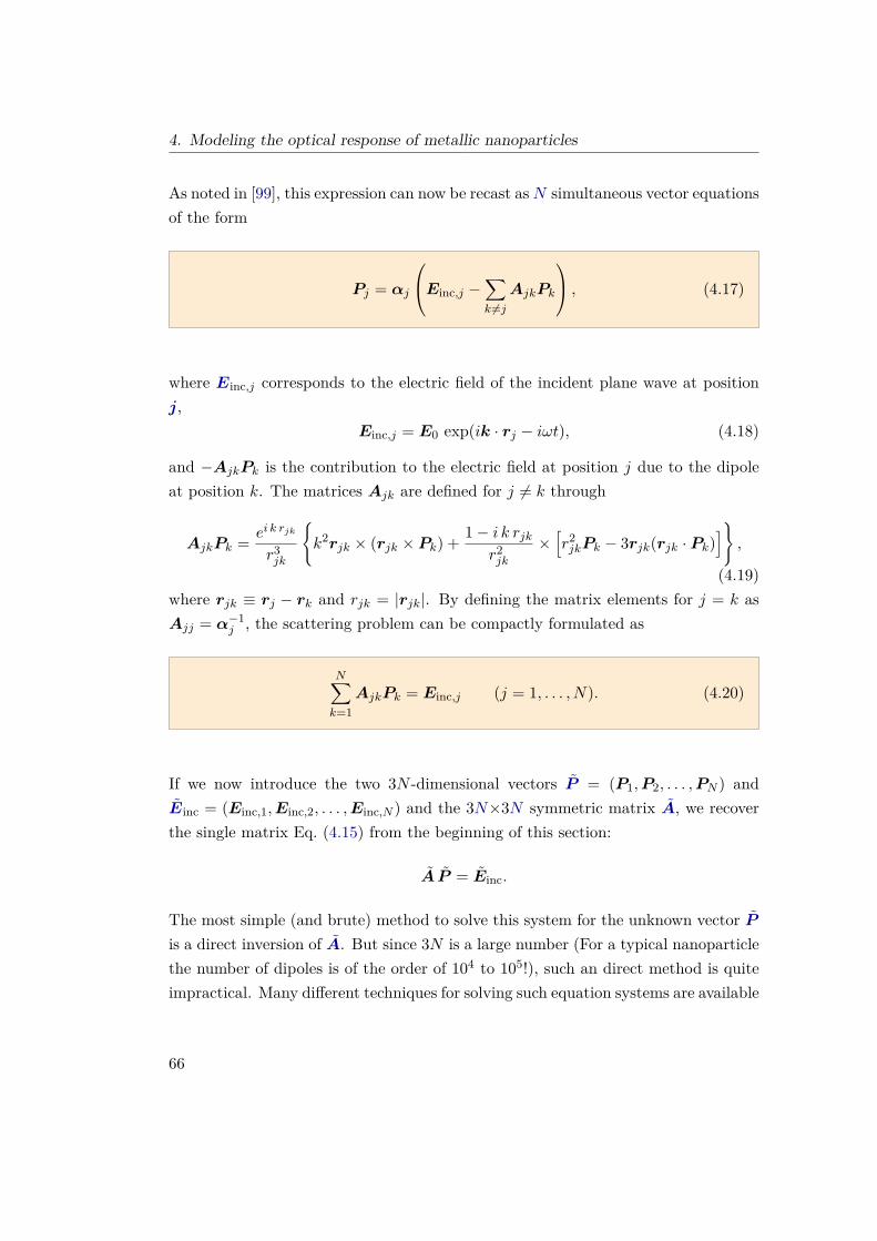
4. Modeling the optical response of metallic nanoparticles
As noted in [99], this expression can now be recast asN simultaneous vector equationsof the form
Pj = αj
Einc,j −∑k 6=j
AjkPk
, (4.17)
where Einc,j corresponds to the electric field of the incident plane wave at positionj,
Einc,j = E0 exp(ik · rj − iωt), (4.18)
and −AjkPk is the contribution to the electric field at position j due to the dipoleat position k. The matrices Ajk are defined for j 6= k through
AjkPk = ei k rjk
r3jk
k2rjk × (rjk × Pk) + 1− i k rjk
r2jk
×[r2jkPk − 3rjk(rjk · Pk)
],
(4.19)where rjk ≡ rj − rk and rjk = |rjk|. By defining the matrix elements for j = k asAjj = α−1
j , the scattering problem can be compactly formulated as
N∑k=1
AjkPk = Einc,j (j = 1, . . . , N). (4.20)
If we now introduce the two 3N -dimensional vectors P = (P1,P2, . . . ,PN ) andEinc = (Einc,1,Einc,2, . . . ,Einc,N ) and the 3N×3N symmetric matrix A, we recoverthe single matrix Eq. (4.15) from the beginning of this section:
A P = Einc.
The most simple (and brute) method to solve this system for the unknown vector Pis a direct inversion of A. But since 3N is a large number (For a typical nanoparticlethe number of dipoles is of the order of 104 to 105!), such an direct method is quiteimpractical. Many different techniques for solving such equation systems are available
66

4.2. Discrete Dipole Approximation
and ddscat uses an iterative method [96]. It begins with a guess (typically P = 0)for the unknown polarization vector, and then iteratively improves the estimate forP until Eq. (4.15) is solved to some error criterion (usually the error tolerance isuser-defined and smaller than 10−5, see [96]). Under some circumstances there maybe problems with the convergence of this iterative method (see [99], for example), soin general convergence tests are necessary to choose the right grid size.
4.2.1. Cross sections with DDA
Once Eq. (4.15) has been solved, the extinction Cext, absorption Cabs, and scatteringCsca cross sections can be computed from the optical theorem. The results can againbe found in [97] and are given by
Cross sections with DDA
Cext = 4πk|Einc|2
N∑j=1=m
(E∗inc,j · Pj
), (4.21)
Cabs = 4πk|Einc|2
N∑j=1
=m
[Pj · (α−1
j )∗P ∗j]− 2
3k3Pj · P ∗j
, (4.22)
Csca ≡ Cext − Cabs, (4.23)
with the wave number k = 2π/λ. When absorption is dominant, it may becomedifficult to calculate Csca with the above subtraction, because then Cext and Cabs
have to be computed with high accuracy. It is also possible to compute the scatteringcross section directly by calculating the power radiated by the array of oscillatingdipoles [97]:
Csca = k4
|Einc|2∫dΩ
∣∣∣∣∣∣N∑j=1
[Pj − n(n · Pj)] e−i k n·rj∣∣∣∣∣∣2
, (4.24)
67

4. Modeling the optical response of metallic nanoparticles
where n is an unit vector in the direction of the scattering, and dΩ is the element ofsolid angle.
68

4.3. Boundary Element Method
4.3. Boundary Element Method
The Boundary Element Method (BEM) has emerged as a powerful numerical tech-nique for solving a wide variety of computational engineering and science problems4.The method has remote deep roots in the history of mechanics5 and its mathematicalfoundations include the theorems of Gauss, Green and Stokes – they allow the basicreduction from volume differential equations to boundary integral equations [100] aswe have already seen in Chap. 3.
Figure 4.3.: After discretizing the particle surface the corresponding continuoussurface charges and currents are approximated as points in the centroids of thesmall surface elements. The Green function connects these different points witheach other, see Eq. (3.38).
The first step in developing the BEM is based upon transforming the consideredset of differential equation [viz. Maxwell’s equations, see Eq. (3.19)] into integralequations [we did this in Eq. (3.24) and Eq. (3.40)]. The new integral expressions arevalid everywhere – inside and outside the domain as well as on its boundary. Nowthe structure of the considered problem comes into play: Usually we can solve theequations inside and outside the domain, the only non-trivial part comes from theboundary (note that this approach is based upon a mathematically rigorous definitionof the integrals as limits to the boundary [100]). As mentioned in Sec. 3.3.1, the BEMis based on an approximation of a continuous surface to a discrete number of pointslocated at the centroids of small surface elements, see Fig. 4.3 – this is the so called
4Examples of application cover the fields of elasticity, geomechanics, structural mechanics, electro-magnetics, acoustics, hydraulics, biomechanics, and much more.
5A short overview about the historical development of the BEM can be found in [100] for example.
69

4. Modeling the optical response of metallic nanoparticles
collocation method, in contrast to the more complex Galerkin approach [100], forexample, where a linear interpolation within the surface elements is used.
Once the surface charges and currents have been derived as discussed in Chap. 3 [seeEq. (3.31) and Eq. (3.44)], we can determine the electromagnetic fields (see Fig. 4.4)and simply compute the scattering, absorption and extinction cross sections from thePoynting vector [66, 88]:
Cross sections for retarded simulation
Csca = nb
∮∂Ω
<e n (E ×B∗) da, (4.25)
Cext = − 1nb
∮∂Ω
<e n (E ×B∗inc +E∗inc ×B) da, (4.26)
Cabs = Cext − Csca. (4.27)
Figure 4.4.: (a) Scattering cross section of a gold nanotriangle (55× 50× 8 nm, nb= 1.34). The panels (b) and (c) show the electric field at the resonance energy of792 nm at the particle surface and on the outside, respectively. (Also see Fig. 3.7.)
Related to this thesis we have developed a Matlab® toolbox called mnpbem forthe simulation of metallic nanoparticles based on the BEM. Further details on thistoolbox can be found in [84] and [88].
70

4.4. Other methods
4.4. Other methods
There exists a whole bunch of other methods for the calculation of light scattering andabsorption of plasmonic structures. The majority of them is based on a discretizationof space (and time). For example with the Finite Difference Time Domain (FDTD)approach the hole space containing the particle together with the time parameterhas to be discretized and Maxwell’s equations are solved in their differential form.Another technique is based on the dyadic Green tensor, which mediates the responsebetween small volume elements of the scatterer. Other approaches are the multiplemultipole method [4], the Method of Moments (MoM), or the multiple scatteringmethod [23].
71
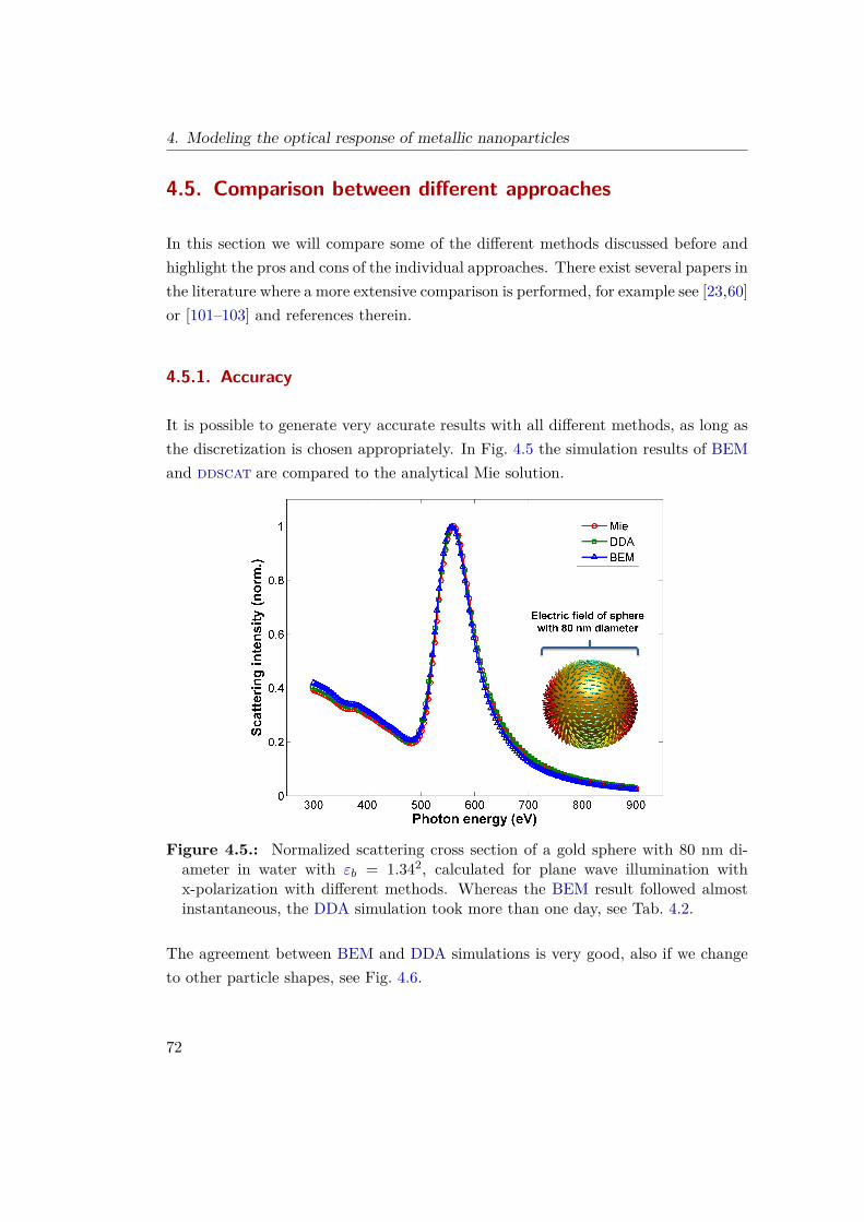
4. Modeling the optical response of metallic nanoparticles
4.5. Comparison between different approaches
In this section we will compare some of the different methods discussed before andhighlight the pros and cons of the individual approaches. There exist several papers inthe literature where a more extensive comparison is performed, for example see [23,60]or [101–103] and references therein.
4.5.1. Accuracy
It is possible to generate very accurate results with all different methods, as long asthe discretization is chosen appropriately. In Fig. 4.5 the simulation results of BEMand ddscat are compared to the analytical Mie solution.
Figure 4.5.: Normalized scattering cross section of a gold sphere with 80 nm di-ameter in water with εb = 1.342, calculated for plane wave illumination withx-polarization with different methods. Whereas the BEM result followed almostinstantaneous, the DDA simulation took more than one day, see Tab. 4.2.
The agreement between BEM and DDA simulations is very good, also if we changeto other particle shapes, see Fig. 4.6.
72

4.5. Comparison between different approaches
Figure 4.6.: Comparison of the normalized scattering cross section calculated withBEM and ddscat for gold rods with changing aspect ratio (left) and a 15 x 15 x8 nm gold cube (right), εb = 1.342.
4.5.2. Performance
A performance comparison for the different methods is a challenging task since allof them have their own assets and drawbacks. In this subsection we will only showscattering results for different particle geometries which we obtained from BEM andDDA simulations. For the DDA simulation we used the previously discussed ddscatprogram. The BEM simulations were carried out with our mnpbem toolbox.
In Tab. 4.1 a computing time comparison for the quasistatic and the full retardedsolution of Maxwell’s equations as discussed in Chap. 3 is shown. Tab. 4.2 is adoptedfrom [60], for details see table caption.
No. of vertices Nr. of faces quasistatic eigenmodeexpansion
full retardedsolution
144 284 2.26 s 0.23 s 8.81 s256 508 4.83 s 0.43 s 32.85 s400 796 16.05 s 0.94 s 103.96 s676 1348 71.82 s 2.82 s 446.38 s
Table 4.1.: CPU time elapsed for a 10 nm sphere with changing discretization fordifferent kinds of BEM simulations, see [84]. The calculations were performed ona standard office PC running on Windows XP with Matlab® R2010b 32-bit.
73

4. Modeling the optical response of metallic nanoparticles
BEM DDA FDTD
Computationaldemand
V 2Nω V 3Nω V ′ω/∆ω
Storage demand V4/3 V 2 V ′
Average CPU timefor 80 nm sphere
1 min 26 h (~2 days) not tested yet
Advantages low computationaland storage demand,
only surface isdiscretized
simpleparametrization, onlyparticle volume is
discretized
simpleimplementation, fullspectrum in single
run
Disadvantages complexparametrization
time consuming,particle size a and εlimited to |a
√ε|/λ < 5
time consuming,difficult to apply toarb. ε(ω), parametr.of outside volume
and ABCs.
Table 4.2.: Critical comparison of the performance of BEM, DDA, and FDTD adoptedfrom [60], where we have added a CPU time comparison. Nω is the number of calculatedfrequencies and V is the particle volume measured in units of the cube of the skin depth[see Eq. (2.9), ζ ≈ 15 nm in the visible near-infrared (see App. A.2 for the frequencyrange of the visible spectrum)]. V ′ is the discretized volume for the FDTD simulationand it extends considerably outside the particle in order to account for light propagationin the surrounding medium [also absorbing boundary conditions (ABCs) have to be ap-plied]. In this table for the BEM and DDA approach a direct inversion of the secularlinear equations is assumed (ddscat uses conjugate gradient algorithms to solve the cor-responding equations in an iterative approach – three different algorithms can be chosenin the current version of ddscat [96]. DDA scales as V log V Nω when using the iterativemethod, whereas BEM scales as V 4/3Nω in this case, see [60]). The factor ω/∆ω in FDTDis proportional to the number of time steps needed to describe a component of frequencyω with frequency resolution ∆ω. For the comparison of a typical average computing timethe optical spectrum of a gold sphere with a diameter of 80 nm and Nω = 150 has beencalculated (particle symmetry has not been exploited). The DDA simulation ran on 32nodes of a Sun Fire V20z cluster with 2 × AMD Opteron 248 2 (2 GHz) processors each(the number in brackets corresponds to the simulation time on only 4 nodes to allow abetter comparison), whereas the BEM simulation was started on a transtec CALLEO 431Lserver with four AMD six-core Opteron F 2431 (2.4 GHz) processors and 64 GB DDR2-667memory. On a standard PC the same BEM simulation takes about 2 minutes, see Tab. 4.1.
74

4.5. Comparison between different approaches
4.5.3. Limits and inaccuracies
The BEM approach is suited for homogeneous and isotropic dielectric environments,where the embedded bodies are separated by sharp boundaries. Besides the compu-tational limitations (for an overview of the Matlab® memory limitations for differentoperating systems consult App. C.1), there are some other points, that are responsi-ble for inaccuracies or difficult (or impossible) to implement. Nevertheless the BEMworks remarkably well and the agreement with experimental data is striking. Here isa short list of possible problems that are inherent to all discussed simulation meth-ods (fortunately they mostly become important only if the nanoparticles are verysmall):
• The sharp and abrupt two dimensional Maxwell boundary conditions becomequestionable for very small particles because of the spill-out effect [91]: Thesurfaces boundary changes to a three dimensional inhomogeneous interface.
• The surface and interface gets charged because of the different chemical poten-tial of the particle and dielectric background (chemical interface damping [104]).
• The dielectric function of a nanoparticle is different from the dielectric functionof bulk material.
• As already mentioned before, the dielectric function ε(ω) is not homogeneous,it is a local spatial dependent function ε(r,r’,ω) and changes continuously whileapproaching the surface or defects in the material [91].
• The idea of a surface charge density or a surface current density is an ideal-ization of macroscopic electromagnetism. In reality the charge or current isconfined to the immediate neighborhood of the surface [66]. (Nevertheless thisidealization works quite well and is an essential part of classical field theory.)
75


5. Imaging of surface plasmons
Maxwell’s equations are about 150 years old, so why (without any intention to beblasphemous) can we still do interesting physics with them? The answer lies in theinterplay with sources: Electromagnetic interactions down at the nanoscale open upthe fascinating field of nanooptics, interactions with quantum objects allow us toenter the prosperous world of quantum optics.
coherent (classical) optics L () > λdiffraction grating L > λphotonic crystals L () < λmetamaterials L λ
Table 5.1.: Characteristic length scales L of different parts of optics compared tothe wavelength λ.
5.1. Principles of near-field optics
In free space, the propagation of light is determined by the dispersion relation~ω = cp = c~k, which connects the wave vector k =
√k2x + k2
y + k2z = 2π/λ of a
photon (for a real lens the wavelength λ must be corrected by the numerical apertureNA) with its angular frequency ω [4]. Heisenberg’s uncertainty principle now alreadypredicts a fundamental resolution limit for optical microscopes: The product of theuncertainty of the momentum of a microscopic particle ∆kx and the uncertainty inthe spatial position ∆x in the same direction cannot become smaller than ~/2:
~∆kx ·∆x ≥~2 . (5.1)
77

5. Imaging of surface plasmons
Since the maximal possible value of kx is the total length of the free-space wavevector 2π/λ, we can rewrite the uncertainty equation to
∆x ≥ 12∆kx
= λ
4π . (5.2)
This states, that the accomplishable spatial confinement for photons is inverselyproportional to the spread1 in the magnitude of the associated wave vector component∆kx.
The expression (5.2) is very similar to the diffraction-limited resolution derived byLord Rayleigh [105] or Ernst Abbe2 [106] in the late 19th century:
∆x = 0.6098 λ
NA . (5.3)
We see that there is some arbitrariness in the definition of a resolution limit: Westarted this discussion with the uncertainty principle of Quantum mechanics, LordRayleigh investigated a grating spectrometer [4], while Abbe based his formulationon the distinguishability of the image pattern of two point dipoles. A simple Fouriertransformation from position to momentum space also leads us to a similar result:
∆kx ·∆x ≥ 1 , =⇒ ∆x ≥ λ
πNA ≈ 0.3183 λ
NA , (5.4)
see [4] for more details. This last expression is almost two times less pessimistic thanEq. (5.3), but it seems that we cannot get a better resolution than approximatelyhalf of the wavelength. Does this predict that there is no reasonable chance toinvestigate objects on the nanoscale without violating fundamental laws of nature?Fortunately the answer is no, there are several ways to elude this limitation. On onehand we can apply some tricks based on the exploitation of distinctive features ofthe investigated objects. For example we can increase the resolution trough selectiveexcitation of two close-by molecules, if they are distinguishable in energy, orientationor something else.
1Such a spread in wave vector components occurs for instance in a light field that converges towarda focus, e.g. behind a lens [4].
2Born 23th January 1840 in Eisenach; † 14th January 1905 in Jena.
78

5.1. Principles of near-field optics
But on the other hand if we look at Eq. (5.2) once again, we see that in theory thereis no limit to optical resolution if the bandwidth of ∆kx is arbitrarily large. In thissense if we include evanescent fields in optical microscopy we are able to increase theresolution limit and to investigate near fields and structures at the nanoscale.
79

5. Imaging of surface plasmons
5.2. How to picture a plasmon
The previously discussed increase of the resolution limit is nicely realized in SNOMexperiments for example, where we are able to map the photonic local density of states(LDOS). Another method that allows to directly picture surface plasmon polaritonsof a metallic nanoparticle is EELS, see Chap. 11. In this approach a beam of electronswith high kinetic energy (of the order of 100 keV) passing by (or through) a metallicnanoparticle excites a plasmon and therefore looses a small fraction of its energy. Bydetecting this energy loss and rasterscanning the electron beam across the particle,we get a picture of the plasmon oscillation.
5.2.1. Mapping the plasmonic LDOS
The principal idea for SNOM is to bring a detector very close to surface of theinvestigated structure – as close that it can detect the evanescent fields. Such andetector can be realized by a fluorophore for example, since its spontaneous emissionrate serves as a direct probe of the photonic LDOS at the fluorophore position.In Chap. 10 we exploit this capability for mapping the plasmonic modes of goldnanoparticles. We use combined regular arrays of identical gold and fluorophore-doped polymer nanoparticles with a slightly different grating constant. This setupallows th generate an optical Moiré pattern corresponding to a 200 × magnified mapof the plasmonic mode, which can be directly imaged with an optical microscope, seeFig. 5.1 and Fig. 10.3.
5.2.2. Electron energy loss spectroscopy
As mentioned above another approach for imaging a plasmon is energy-filtered trans-mission electron microscopy in the low-energy-loss region of EELS experiments. Byvarying the position of the high energetic electron beam one can once again map outthe evanescent fields. This was first demonstrated by [107] and [108] in 2007, seeFig. 5.2.
The dispersion relation of a free electron does not cross the light cone at any point [23],so at first it is not obvious how to couple an electron with light. Besides nonlinear
80

5.2. How to picture a plasmon
Figure 5.1.: Principal scheme of optical Moiré effect and the discussed MNP andfluorophore arrays lying upon another together with Eq. (10.1). For a detaileddiscussion see Chap. 10.
Figure 5.2.: First reported plasmon mapping with EELS experiments. Figurestaken from [107] (a) and [108] (b).
processes or electrons with less momentum than their free counterpart (e.g. fromphotoemission) it is particularly the interaction with light with higher momentum(evanescent fields) that allows the interaction.
The high-energetic electrons move with 70 - 80 % of the speed of light and thusrelativistic effects come into play. During one plasmon oscillation the swift electronsare able to move about 100 nm – this is sufficient for the plasmon-electron interaction,a process reminiscent of a self energy schematically shown in Fig. 5.3. In a quantumpicture, the electron loses energy through the excitation of a surface plasmon. Inthe classical picture the electron has to perform work against the field of the excitedplasmon and thus loses a little bit of its energy. In [109] it is shown that a quantummechanical description of EELS yields the same results as a semiclassical formalismif all the inelastic signal is collected [23]. This allows us to simply incorporate the
81

5. Imaging of surface plasmons
relativistic motion of the electrons to our BEM approach in terms of the Liènard-Wiechert potentials. We calculate the induced electric field at the positions of theelectron beam and can express the energy-loss probability through the work againstthis field, see Eq. (11.1).
Figure 5.3.: Principle of EELS interaction: The electron beam excites a surfaceplasmon which in turn acts back on the electrons at a later position. The expressionof the electron charge %ext corresponds to a charged wire.
In the time domain the electron beam interacts with a surface plasmon oscillating intime, whereas in the frequency domain the plasmon oscillation becomes frozen andthe electrons interact with a periodically modulated charge distribution as indicatedat the expressions for the electron charge in Fig. 5.3. It is important to notice thatwe get a nonlocal interaction here, the electron at position re induces the plasmonicfield which acts back on the electron at a later time at position r′e. In this sense theenergy loss probability can be expressed through the integral over the imaginary partof the induced Green tensor [110,111] at the beam position r0 = (x0, y0):
Electron energy loss probability in terms of Green function
Γ(r0, ω) ∝∫dt dt′ =m
eiω(t′−t)Gind[re(t), re(t′);ω]
, (5.5)
82

5.2. How to picture a plasmon
which directly follows from Eq. (11.1). As discussed in Chap. 11 we calculated theenergy loss for a rod-shaped particle in comparison to STEM EELS and EFTEMmeasurements performed by the Felmi group at the Technical University Graz. InFig. 5.4 we show the results of experiment and theory, which once again match quitenicely.
Figure 5.4.: Comparison of measured and simulated EFTEM maps as described inChap. 11. On the left we see the plasmon dipole mode with an energy of about 1eV, in the middle the quadrupole mode at around 1.5 eV and the octupole modeat 2.4 eV on the right.
There has been some discussion if the EELS signal directly renders the photonicLDOS [110,111]. It turns out, that – although intimately related – there is no directlink between EELS and LDOS maps, and that EELS can even be blind to hot spotsin the gap between coupled nanoparticles [110].
For the bonding plasmon mode plotted on the left side of Fig. 5.5 the fields in thegap region are very strong, resulting in a very high LDOS. The EELS signal on thecontrary is completely blind to the hot spot. For the antibonding mode on the righthand side the behavior changes to the opposite: Because of the vanishing fields the
83

5. Imaging of surface plasmons
Figure 5.5.: The lower panels show EELS and LDOS maps for the bonding (a)and antibonding modes (b) of coupled nanoparticles. In the upper panels thecorresponding scalar potential and electric field is plotted. As discussed in [110],the EELS signal is connected to the scalar potential whereas the photonic LDOSmeasures the electric field.
LDOS drops in the gap, whereas the EELS rate has a pronounced maximum [110].
84

5.2. How to picture a plasmon
Why is the kinetic energy of the electrons in EELS experiments so high? In fact,surface plasmons can also be excited by electron beams with lower energies (e.g.reflection EELS experiments3 with energies of 1000-2000 eV). But in transmissionEELS the electron has to pass through the material and the smaller the electronwavelength the better the resolution, see Fig. 5.6.
Figure 5.6.: Excitation of surface plasmons through the transmission of swiftelectrons in thin films [21,22]. The incoming wave vector kel transfers the com-ponent kq to the thin film. The energy of the surface plasmon is determinedby the projection kx to the surface and the dispersion relation 2.6.
Note that for particle plasmons there is no momentum conservation, see Chap. 2.
Additional remark
3In 1956 Powell [30] investigated inconsistencies in the EELS spectra of transmission and reflectionEELS experiments which lead to the experimental verification of surface plasmons.
85


6. Influence of surface roughness
It is nearly impossible to fabricate perfectly smooth nanoparticles, thus it is quiteimportant to discuss the influence of surface roughness on the optical propertiesof MNPs. Especially if e-beam lithography (see App. B.2) is used to produce theparticles, the resulting metal structures are polycrystalline and the surfaces are quiterough. Contrary to our first guess we found out that a moderate amount of surfaceroughness has no significant impact on the far-field optical properties of MNP. InChap. 12 we show that this behavior can be interpreted as some kind of plasmonicaveraging over the random height fluctuations of the rough metal surface (motionalnarrowing).
6.1. Generation of a rough particle in the simulation
To allow systematic investigations of surface roughness on metallic nanoparticles, weneed to control and quantify the “amount” of roughness on a surface. One possi-bility to do this is to add (controllable) stochastic height variations to the smoothsurface of an ideal nanoparticle. Let us exemplify the idea for the 2D case: Weassume that the height of each vertex of a triangulated plate is given by a functionh(x, y). The mean value should vanish 〈h(x, y)〉 = 0 and the value of h at (x′, y′)should be correlated to the value at position (x, y) through a distance dependentfunction: 〈h(x, y)h(x′, y′)〉 = f(x − x′, y − y′). This requirements are all fulfilled ifwe introduce a Gaussian autocorrelation function and attach arbitrary phase factorsto all Fourier coefficients. In this way we are able to average the z-coordinate ofeach vertex corresponding to this random potential and we have two parameters tocontrol the roughness, the standard deviation of the Gaussian function ς (determines
87

6. Influence of surface roughness
the amount of roughness) and a height scaling parameter ∆h (assigns the deepnessof the asperity).
Wrapping the created roughness around the surface of a nanorod, we get the structureshown in Fig. 6.1.
Figure 6.1.: Triangulated nanorod with smooth surface and stochastic height vari-ations generated with a random Gaussian potential. Problems in the simulationmay arise if sharp features are present.
Unfortunately very sharp features in the triangulated mesh may lead to inaccuraciesin the simulation and may cause diverging surface charge densities. Luckily we getan even better result without sharp peaks, if we do not directly interpolate the heightof each vertex with the Gaussian autocorrelation, but rather generate a box aroundthe particle and interpolate the stochastic vertex height with respect to this box, seeFig. 6.2.
Figure 6.2.: Generating a box around the smooth particle and interpolating stochas-tic vertex heights with respect to this box gives a much better result without sharpfeatures as in Fig. 6.1. The random height variations are again controllable by pa-rameters of the Gaussian autocorrelation, see Eq. (6.1).
Again we use a normal probability density function multiplied with N random phases
88

6.1. Generation of a rough particle in the simulation
eiφrnd (for each spatial direction)
Generation of surface roughness
h(x, y, z) = 1N<eF−1
[e−
12 ς
2(k2x+k2
y+k2z) eiφrnd
]− 1
2
, (6.1)
where F−1 denotes the inverse Fourier transform, N is a normalization factor andς2 is the variance of the height fluctuations. For the arbitrary phase factors φrnd theMatlab® built-in function rand(n) to create uniformly distributed pseudorandomnumbers has been used.
We next interpolate the scaled stochastic height variations ∆h · h(x, y, z) to thenanoparticle surface and displace the vertices of the nanoparticle along the surfacenormal directions. The influence of ∆h and ς is shown in Fig. 6.3.
Figure 6.3.: Surface roughness generated with Eq. (6.1) for changing parameters.
89

6. Influence of surface roughness
Another possibility for the simulation of “realistic” particles is based on the extrac-tion of their contour out of scanning electron microscope (SEM) images, see Fig. 12.1.The triangulated particle is generated by assigning a certain height profile (with arounded transition to the top and bottom area, see [84]) to the extracted contour-polyline and wrapping a mesh around the structure. A SEM image together withthe extracted contour and the final BEM particle is shown in Fig. 6.4.
Figure 6.4.: (a) SEM image of a rod-shaped nanoparticle fabricated by e-beamlithography (see Appendix B.2). (b) Contour extraction and (c) creation of thecorresponding triangulated particle for a BEM simulation.
90

6.2. Theoretical analysis of surface roughness
6.2. Theoretical analysis of surface roughness
Let us for one moment take only the mean value of the height difference of bumps orhollows at a rough surface as an indicator for the degree of roughness. For a mediumsized nanoparticle this mean value is of the order of nanometers. One possibility todescribe the optical properties of structures with such small features1 is presentedin [112], for example. By writing the dielectric constant ε(k,ω) as a function ofboth the wave vector k and the angular frequency ω, the authors incorporate theeffect of small features via the spatially nonlocal response of materials to Maxwell’sequations2.
On the other hand we can also understand the influence of rough surfaces if we onceagain consider the eigenmode expansion discussed in Sec. 3.3.2. We can model therough surface as a distortion of the surface ∂Ω from its ideal shape, see Chap. 12.The surface derivative of the Green function F then changes to F+δF .We want to determine, how the peak position of the plasmons is affected in case ofsurface roughness and since this peak position is assigned by the plasmon energy, weneed to investigate the modification of the Eigenvalue λk. For sufficiently small δFwe can employ a perturbation analysis, where we treat F as the unperturbed partand δF as the “perturbation”. This calculation is carried out in Sec. 12.4, and theresult is shown in Fig. 12.3.
Our findings show a surprisingly small effect for the influence of surface roughness onthe position and width of the plasmon peaks of metallic nanoparticles. We identifiedthe reason for this as motional narrowing3, where the plasmon averages over therandom height fluctuations h.
1So-called finite size effects have been phenomenologically accounted for by increasing the dampingrate of the conduction electrons contribution to the permittivity, see [44].
2Their implementation is based on the self-consistently solved hydrodynamic Drude model3This behavior is known from electron-hole pairs in semiconductor quantum wells [113], where thepropagating excitons “average” over the random potential of local monolayer fluctuations, whichresults in a narrowing of the exciton lineshape.
91


7. Nonlinear optical effects of plasmonicnanoparticles
The light-matter interaction between MNPs and an electromagnetic wave happenson a very fast time scale and, as we have discussed in Sec. 2.4, already after a fewfemtoseconds the plasmonic excitations start to vanish again. The temporal evolutionand this ultrafast relaxation of surface plasmon polaritons is of central importancefor many kinds of plasmonic applications.It is amazing that we can explore such rapid dynamic processes with experimentsnowadays. One way to enter the ultrafast world of plasmon dephasing is given bynonlinear autocorrelation measurements, which allow to determine sub-10 fs decaytimes. Usually a bandwidth-limited laser pulse working in the few-cycle regime isused to excite nonlinear effects which serve as a non-invasive monitor for the plasmondynamics [46].
The simplest nonlinear effect is second-harmonic generation (SHG), where a nonlinearmaterial absorbs two photons of frequency ω and emits a new photon of frequency2ω. But because of the inversion symmetry in the atomic arrangement of metals,SHG is forbidden in the bulk [46, 114, 115]. However the symmetry is broken at thesurface and so a second order dipole response can exist in the surface region. Therecan be electric dipolar surface contributions due to the broken symmetry or alsohigher order bulk signals can contribute the second-order nonlinearity [46], but thelatter are known to be much weaker and can therefore be neglected.Breaking the symmetry of centrosymmetric media also allows a second-order signalfor a perfectly symmetric nanosphere for example, it will just strongly depend ondefects, facets and other small deviations from the spherical shape [116]. This defectdependence will give a huge varying signal for different particles of the same shape.Another example of SHG measurements for systems with a broken symmetry has
93

7. Nonlinear optical effects of plasmonic nanoparticles
been reported by [117], where they investigated arrays of noncentrosymmetric T-shaped gold nanodimers.
On the other hand third-harmonic generation (THG), the next higher nonlinear pro-cess where a mixing of four fields (E ∝ χ(3)E3) occurs, is allowed in all media andnot restricted to symmetry considerations, see Fig. 7.1. Supported by the abovementioned reasons the χ(3) nonlinearity for gold nanoparticles is also much strongerthan the corresponding SHG signal [78], which makes THG a perfect candidate toinvestigate the femtosecond dynamics of particle plasmons.
Figure 7.1.: (a) SEM image of a gold bowtie nanoantenna. (b) and(c) measuredTHG intensity for linear polarization along long and short axis respectively. Thelower insets show the corresponding simulation results, further details see Chap. 13.(Measurements by Tobias Hanke, University of Konstanz.)
The first observation of third-harmonic signals from individual gold colloids down to40 nm diameter can be found in [116] and a phenomenological macroscopic theory ofoptical second- and third-harmonic generation from cubic centrosymmetric crystalshas been discussed by [118].
94

7.1. Autocorrelation
7.1. Autocorrelation
To measure the autocorrelation the sample is excited by two sequenced laser pulseswith a varying time delay t′ between the pulses. The collected intensity is given bythe interfering electric fields to the power of four (second order autocorrelation G2)or to the power of six (third order autocorrelation G3) and averaged over the detectorresponse time T [46]:
Second and third order autocorrelation function
SHG: G2(t′) = 1T
+T∫−T
[E(t) + E(t− t′)
]4dt, (7.1)
THG: G3(t′) = 1T
+T∫−T
[E(t) + E(t− t′)
]6dt. (7.2)
This pulse interference can also be described by a simple harmonic oscillator model(see [46]). By inserting harmonic fields in the above expressions for G2 or G3 thecharacteristic peak ratio of 1:8 for SHG or 1:32 for THG follows directly from thein and out of phase expression of the electric fields. In Fig. 7.2 the measured andsimulated result of G3 for three different nanoantennas is shown.
Figure 7.2: Third order auto-correlation for three differentnanoantenna geometries, seeTab. 13.1 for spatial dimen-sions and further details. (a)Experimental and (b) sim-ulation result. (Figure byTobias Hanke, University ofKonstanz.)
95

7. Nonlinear optical effects of plasmonic nanoparticles
7.2. Third harmonic imaging
In Chap. 13 we discuss the third harmonic emission of five different antenna struc-tures. We show, that the THG intensity differs significantly for the different struc-tures and that the knowledge of the plasmon damping time (obtained from auto-correlation measurements) suffices, to explain the differences. The principal schemefor this experiment is depicted in Fig. 7.3. An array of nanoantennas (varying insize with different gap distances) gets illuminated by a laser pulse and the nonlinearemission intensity is collected.
Figure 7.3.: Principle of third harmonic imaging as described in Chap. 13. Thefew-fs pulse of a pump laser excites a nanoantenna and the nonlinear emission getscollected. By raster scanning the laser pulse over a sample of varying antennageometries the most resonant structure for this excitation can be picked – seeTab. 13.1.
Anyhow, also the dielectric environment of the metallic particles can contribute tothe nonlinear emission, but the susceptibility of air or fused silica is at least severalorders of magnitude weaker than the one for gold:
96

7.2. Third harmonic imaging
χ(3) ≈ 10−11 esu for gold [119],
χ(3) ≈ 10−14 esu for fused silica [120],
χ(3) ≈ 10−18 esu for air [121].
Nonlinear emission spectroscopy emerges as a new powerful tool for the spatiotempo-ral characterization of nanoantennas. As described in Chap. 13, we demonstrate thatnot the shape but the volume of the nanoantennas plays a crucial role for the deter-mination of the nonlinear emission intensity. Due to radiative damping the structurewith the lowest active volume generates by far the strongest THG emission.
In [116] it has been stated that THG signals also serve as label for bio-sensors andmay be used for the tracking of single molecules. Placing an emitter in the gap regionof the nanoantennas (see Fig. 7.4) may also be one of the next steps for our analysis(also see [57]).
Figure 7.4.: Schematic representation of a bowtie nanoantenna used as one offive different antenna geometries in Chap. 13. One half of the antenna shows thesurface charge distribution at the resonance energy (the bonding mode is clearlyvisible), whereas the other half depicts the surface discretization needed for thesimulation with the BEM.
97


Part II.
Paper reprints
99


In the next chapters reprints of the following papers are included:
• Jan Becker, Andreas Trügler, Arpad Jakab, Ulrich Hohenester,and Carsten SönnichsenThe Optimal Aspect Ratio of Gold Nanorods for Plasmonic Bio-sensingPlasmonics 5 (2010) 161
• Arpad Jakab, Yuriy Khalavka, Jan Becker, Andreas Trügler, ChristinaRosman, Ulrich Hohenester, and Carsten SönnichsenHighly sensitive plasmonic silver nanorodsACS Nano 5 (2011) 6880
• Daniel Koller, Ulrich Hohenester, Andreas Hohenau, Harald Ditl-bacher, Frank Reil, Nicole Galler, Franz Aussenegg, Alfred Leit-ner, Andreas Trügler, and Joachim KrennSuperresolution Moiré Mapping of Particle Plasmon ModesPhysical Review Letters 104 (2010) 143901
• Bernhard Schaffer, Ulrich Hohenester, Andreas Trügler, andFerdinand HoferHigh-Resolution Surface Plasmon Imaging of Gold Nanoparticles by EnergyFiltered Transmission Electron MicroscopyPhysical Review B 79 (2009) 041401(R)
• Andreas Trügler, Jean-Claude Tinguely, Joachim Krenn, AndreasHohenau, and Ulrich HohenesterInfluence of surface roughness on the optical properties of plasmonic nanopar-ticlesPhysical Review B 83 (2011) 081412(R)
101

• Tobias Hanke, Julijan Cesar, Vanessa Knittel, Andreas Trügler,Ulrich Hohenester, Alfred Leitenstorfer, and Rudolf BratschitschTailoring spatiotemporal light confinement in single plasmonic nanoantennasNano Letters 12 (2012) 992
Other parts of this work that are not included here are published in:
• Ulrich Hohenester and Andreas Trüglermnpbem – A Matlab toolbox for the simulation of plasmonic nanoparticlesComputer Physics Communications 183 (2012) 370
• Jürgen Waxenegger, Andreas Trügler, and Ulrich HohenesterMapping exciton wavefunctions in semiconducting carbon nanotubes with plas-monic nanoparticlesPhysical Review B 83 (2011) 245446
• Andreas Trügler and Ulrich HohenesterStrong coupling between a metallic nanoparticle and a single moleculePhysical Review B 77 (2008) 115403
• Ulrich Hohenester and Andreas TrüglerInteraction of single molecules with metallic nanoparticlesIEEE Journal of Selected Topics in Quantum Electronics 14 (2008) 1430
102

8. PAPER: The optimal aspect ratio ofgold nanorods for plasmonicbio-sensing
Jan Becker1, Andreas Trügler2, Arpad Jakab1, Ulrich Hohenester2,and Carsten Sönnichsen1
1 Institute of Physical Chemistry, University of Mainz, Jakob-Welder-Weg 11, 55128 Mainz, Germany2 Institut für Physik, Karl–Franzens–Universität Graz,Universitätsplatz 5, 8010 Graz, Austria
Published in: Plasmonics 5, 161 (2010)
Abstract
The plasmon resonance of metal nanoparticles shifts upon refractive index changesof the surrounding medium through the binding of analytes. The use of this prin-ciple allows one to build ultra-small plasmon sensors that can detect analytes (e.g.,biomolecules) in volumes down to attoliters. We use simulations based on the bound-ary element method to determine the sensitivity of gold nanorods of various aspectratios for plasmonic sensors and find values between 3 and 4 to be optimal. Experi-ments on single particles confirm these theoretical results. We are able to explain theoptimum by showing a corresponding maximum for the quality factor of the plasmonresonance.
103

8. Optimal aspect ratio for bio-sensing, Plasmonics 5, 161 (2010)
8.1. Introduction
Gold nanoparticles have a long history as optical or electron microscopy labels. Morerecently, their plasmon resonance has been employed for more elaborate opticalnanoscopic sensing schemes. The plasmon resonance of coupled particles dependson interparticle distance [122–125], and the strong plasmonic light scattering effi-ciency allows for the visualization of single nanorods, for example for orientationsensing [126–129]. Furthermore, the resonance position is influenced by the particlecharge [130,131] and the refractive index of the particle’s immediate environment [51].The plasmonic sensitivity to the immediate dielectric environment of the particles al-lows one to monitor the dielectric constant of liquids and binding events of moleculesto the gold particle surface. Here, the nanoparticle sensor acts in a way similar tosensors exploiting the surface plasmon resonance on gold films, which is a standardmethod in many laboratories. However, whereas the detection scheme for surfaceplasmon resonance is usually a shift in the plasmon excitation angle [132], plas-monic nanoparticles show a shift in the plasmon resonance frequency [133]. Themain advantage of using nanoscopic particles as sensors instead of metal films istheir extremely small size which allows one, in principle, to measure analytes in vol-umes as small as attoliters [134]. The key factor for taking advantage of the smalldetection volume of plasmonic particles is the single particle plasmon-scattering spec-troscopy [133,135]. Single particle measurements probe the local environment aroundone specific particle, which – in principle – enables massive parallelization of nanopar-ticle plasmon sensors either for analyzing different analytes or obtaining statistics.Recently, we demonstrated a scheme that can conduct parallel sensing on randomlyarranged nanoparticles using a liquid crystal device as an electronically addressableentrance shutter for an imaging spectrometer [136].For such dielectric plasmon nanoparticle sensors, one hopes to have a large spectralshift for a given amount of analyte or refractive index change of the environment.Initially, spherical gold particles were used [134,137] but were soon replaced by goldnanorods [138] due to their higher sensitivity on refractive index changes [139]. Alot of effort has been applied towards identifying the ideal plasmon sensor with alarge spectral shift for a given change in refractive index, for example, using rod-shaped gold nanorattles [140], metamaterials [141], silver-coated gold nanorods [142]
104

8.2. Plasmon sensor quality
and others. However, rod-shaped nanoparticles remain popular for plasmonic ap-plications. Some reasons for this are the ability to fabricate gold nanorods in highquality using seeded crystallization from solution, the adjustability of the plasmonresonance by varying the aspect ratio, the strong scattering efficiency, and the lowplasmon damping in nanorods.
Here, by means of simulations and experiments, we investigate which aspect ratio(AR) of gold nanorods is ideal for plasmonic sensing by employing various measuresfor ’ideal’ behavior. There are several different quantities that describe the perfor-mance of a plasmonic structure for sensing applications on a single particle level –and all of them have their merits for certain applications. We will discuss the mostimportant of them in the following paragraphs – the plasmonic sensitivity to refrac-tive index change as well as various ’figures of merit’ – and present their dependencyon nanorods’ geometry from calculations for spherically capped gold rods with theBoundary Element Method (BEM) [82, 83]. We confirm the identified trends by ex-perimental results obtained using single particle dark field scattering spectroscopy.
8.2. Plasmon sensor quality
Changing the refractive index n of the embedding medium by a given amount, dnshifts the plasmon resonance position in wavelength or energy units (λres, Eres, re-spectively, see Fig. 8.1 a). The corresponding proportionality constant or sensitivitySλ (often simply denoted ∆λ/RIU) can be expressed in wavelength (Sλ) or energy(SE) units [143]: Sλ = dλres/dn and SE = dEres/dn = Sλ
dEdλ = −Sλ/λ2 × 1, 240 nm/eV.
The relatively broad plasmon linewidth Γ (full width at half maximum) complicatesthe analysis further, because the plasmon linewidth of nanostructures with differentgeometries can vary more than tenfold. Since it is easier to detect a given resonanceshift for narrow lines, the resonance shift relative to the linewidth is a more mean-ingful measure of the sensoric quality. This dimensionless quantity is often referredto as the ’figure of merit’ (FOM) = S/Γ [144].The FOM is easily determined experimentally and allows for the comparison of theplasmonic properties of many different structures with a single sharp plasmonic res-onance. For more complex plasmonic responses (such as in metamaterial structures
105

8. Optimal aspect ratio for bio-sensing, Plasmonics 5, 161 (2010)
based on an analog of electromagnetically induced transparency (EIT) [141]), wherethe plasmon resonance does not follow a simple Lorentz peak shape, the conceptneeds to be refined. In practice, one would normally detect a spectral shift of aresonance as a relative intensity change dI/I at a fixed wavelength λ0 induced by asmall index change dn. We can therefore define an alternative dimensionless figureof merit:
FOM∗ =(dI/dn
I
)max
=(Sλ (dI/dλ)
I
)max. (8.1)
The wavelength λ0 is chosen such that FOM∗ has a maximum value – for goldnanorods in the shoulder of the resonance of the long-axis plasmon near the placewhere the slope dI/dλ is highest.Bio-sensing applications are even more complex. In this case, one seeks to detect thebinding of small (organic) molecules to the nanoparticle surface instead of exchangingthe entire embedding medium. The spectral shift now depends on the relative size ofthe molecules to the volume the plasmon field penetrates into the medium. Further-more, the sensitivity is reduced with increasing distance to the particles surface. A’figure of merit’ trying to capture the different sensing volumes of various nanostruc-tures can be defined as the FOM∗layer for a homogeneous coating of molecules witha specific refractive index (for example, n = 1.5, typical for organic molecules) in alayer of thickness l around the particle normalized to this layer thickness. The formaldefinition of this ’figure of merit for thin layers’ FOM∗layer is therefore:
FOM∗layer =(dI/I
dl
)max. (8.2)
To compare the general sensing quality of different nanostructures, the limit ofFOM∗layer for l → 0 gives a defined value. Table 8.1 summarizes the different quanti-ties used to determine the quality of plasmon sensors and their definitions.
106
8.3. Results
8.3. Results
We simulate the light scattering cross-sections of gold nanorods by solving Maxwell’sequations using the BEM and tabulated optical constants for gold [41]. Regardingshape, we use rods with spherical end-caps varying the particle length while keepingthe diameter constant at 20 nm. Even though the exact end-cap geometry influencesthe resonance position [145], many researchers have successfully used spherical end-caps for their simulations [146]. We vary the aspect ratio by changing only the particlelength because gold nanoparticle synthesis usually results in particles of comparablewidth. From the BEM calculations, we find a linear relationship between aspectratio AR and plasmon resonance wavelength: λres/nm = 505 + 114 (AR − 1). Thecalculations of the layer effect for FOM∗layer were performed within the quasi-staticapproximation (QSA) for spheroids [147] since we did not implement coated particlesin our BEM simulations so far. However, comparisons of QSA with full solutions forthe Maxwell equations have shown good qualitative agreement [145].
The plasmon sensitivity in wavelength units Sλ (calculated with BEM) shows the ex-pected steady increase for an increasing aspect ratio [139] (not shown here), whereasthe sensitivity in energy units SE shows a maximum at an aspect ratio of ARmax = 3(Fig. 8.1). Both the ’classical’ FOM and the more general FOM∗ show the same trendwith two maxima (Fig. 8.2 a). The classical FOM has a maximum for rods with anaspect ratio of AR = 4.3 and a second local maximum at AR = 3.2. The maximaof the generalized FOM∗ is slightly shifted to rod aspect ratios of AR = 4.2 / 3.1 (cf.Table 8.1). The values of the ’figure of merit for small layers’ FOM∗layer (obtained byQSA calculations) are shown in Fig. 8.2 b for increasing layer thickness l and showmaxima at the aspect ratios of AR = 3.0 and AR = 4.3. The first maximum atAR = 3.0 is higher for thin layers and in the limit of layer thickness l → 0. Hence,rods with aspect ratios in the range of 3 to 4 are the best candidates to investigatechanges in the refractive index of the embedding medium.
To verify the theoretical conclusions given above, we compared the theoretical re-sults with experimental values measured on single particles. The particle spectrawere obtained for nanorods immobilized on a glass substrate and exposed to liquidswith various refractive indices in a dark field microscope coupled with an imagingspectrometer [135, 136]. The resulting values are shown in Fig. 8.3 and show the
107

8. Optimal aspect ratio for bio-sensing, Plasmonics 5, 161 (2010)
Figure 8.1.: (a) The plasmon resonance shifts (∆λ) upon changing the refractiveindex of the surrounding medium by dn. To detect such changes, the sensitivitySλ = ∆λ/∆n needs to be large. Other important parameters that characterizeplasmonic sensors are the plasmon linewidth Γ and the wavelength λ0 where therelative intensity change |∆I/I| is largest (see text). (b) The plasmonic sensitivityin energy units SE shows a maximum for gold nanorods with aspect ratio AR= 3.0. The blue line shows data calculated with the BEM, assuming gold rodswith a diameter of 20 nm and spherical end-caps embedded in water (n = 1.33). Asimilar trend is found for a simple calculation using the QSA and a Drude dielectricfunction for gold (black line).
same trend as predicted by the BEM simulations. The values are generally lowerthan the calculated values due to the influence of the supporting glass substrate andare potentially also influenced by a thin organic coating of the particles remainingfrom the synthesis. The variance within the experimental results is not a measure-ment error but originates from small derivations from the ideal particle geometryand environment. For example, defects in the nanoparticles’ crystal structure wouldincrease damping, therefore broadening the plasmon resonance and reducing FOMand FOM∗.
8.4. Discussion
The existence of a maximum of the plasmon sensitivity in energy units can be derivedfrom a simple calculation of the polarizability of a spheroid in quasistatic approxi-
108

8.4. Discussion
Figure 8.2.: To identify the optimal aspect ratio for plasmon sensing, various ’figureof merits’ (FOM) are calculated. (a) The classical FOM defined as plasmon sen-sitivity S divided by plasmon linewidth Γ (left axis) is compared to a generalizedFOM∗ defined as the maximal relative intensity change |∆I/I| for a small refractiveindex change ∆n (right axis). While the classical FOM has a maximum for anaspect ratio of AR = 4.3 and a second maximum at AR = 3.2, the generalizedFOM∗ has its maximum at AR = 4.2 with its second local maximum at AR = 3.1.(b) The FOM∗layer takes into account the sensing volume by considering the plas-mon change induced by a small layer around the particle normalized to the layerthickness (0.01 nm < l < 10 nm in 1 nm steps). The plasmon sensing qualityFOM∗layer decreases with increasing layer thickness (inset) and shows a maximalvalue of FOM∗layer = 0.55 for d → 0 at an aspect ratio AR = 3.0. (Data for a arecalculated with the BEM for gold nanorods with spherical end-caps and 20 nmdiameter, data for b within the QSA for spheroids.)
mation: The polarizability α of a spheroid within the QSA is given by [93]:
α = V
4πεr − 1
1 + L(εr − 1) , (8.3)
where, V is the particle volume, εr = εparticle/εmedium is the relative dielectric functionof the particle with respect to the medium, and L is a shape factor. The exactequation for L is given by [148]:
L = 1AR2 − 1
AR
2(AR2 − 1)1/2ln[AR + (AR2 − 1)1/2
AR− (AR2 − 1)1/2
]− 1
. (8.4)
For AR < 8, this formula is simplified to L ≈ (1+AR)−1.6 with an error of < 5% [42].Equating the real part of the denominator of Eq. (8.3) to zero and using the Drude
109

8. Optimal aspect ratio for bio-sensing, Plasmonics 5, 161 (2010)
Table 8.1.: Summary of the different quantities describing the quality ofplasmon sensors regarding their ability to detect changes in their environ-ment: sensitivity Sλ and SE in wavelength and energy units, the figures ofmerit as classical definition (FOM), in generalized form (FOM∗), and forthin layers (FOM∗layer).
Quantity Definition ARopt Max value
Sλ dλres/dn ∞
SE dEres/dn 3.0 (4.4) 0.85 eV/RIU
FOM Sλ/Γλ = SE/ΓE 4.3 (3.2) 11.1 (10.9)
FOM∗(dI/Idn
)max
4.2 (3.1) 24 (23)
FOM∗layer liml→0
(dI/Idl
)max
3.0 (4.3) 0.57/nm
The last columns list the optimal aspect ratio ARopt (the value in bracketcorresponds to the second maximum) for gold nanorods with 20 nm diame-ter in an aqueous environment and the value of the corresponding quantityat the maximum (see Sec. 8.3 and Sec. 8.4).
Figure 8.3.: Experimental data (each black dot represents one single particle) for thefigures of merit FOM (a) and FOM∗ (b) obtained by single particle spectroscopyin a dark field microscope (inset). The absolute values are slightly lower than thetheoretical prediction (blue line, see also Fig. 8.2 a) due to the attachment of thegold rods to a glass substrate which limits the accessible surface (inset).
model to describe the dielectric function of the particle (Re(ε) ≈ ε∞ − ωp2/ω [42]),the resonance position Eres, the plasmon sensitivity SE , and the aspect ratio with
110

8.4. Discussion
the highest SE value ARmax follow:
Eres = ωp√n2b/L + ε∞ − n2
b
, (8.5)
SE = d
dnbEres = ωp nb (1/L− 1)
(n2b/L + ε∞ − n2
b)3/2, (8.6)
ARmax =(
n2b
n2b + 2 ε∞
)−1/1.6
− 1. (8.7)
where, ωp and ε∞ are the plasma frequency of the conduction electrons (9 eV forgold [149]) and the polarizability of the inner electrons (9.84 for gold [150]), respec-tively, and nb = √εmedium the medium’s refractive index.The agreement of these simple calculations with the BEM calculations is surpris-ingly good (Fig. 8.1 black lines) since the quasistatic approximation is only validfor spheroidally shaped particles much smaller than the wavelength of the incidentlight. The particles we investigate are neither spheroids nor much smaller than thelight wavelength (only a factor of up to 5). Our BEM calculations using sphericallycapped cylinders model the real particle shape more realistically and correctly takethe particles’ absolute size into account.
Interestingly, the aspect ratio with the highest plasmon sensitivity in energy unitsARmax depends on the polarizability of the inner electrons of the metal ε∞ and therefractive index of the medium. For water (nb=1.33) as a medium, the optimal aspectratio becomes ARmax = 3.8. Since the Drude model does not include the contributionof interband damping to the imaginary part of the dielectric function, we concludethat the maximum in plasmonic sensitivity SE is not caused by the effect of thoseinterband excitations.Yet, what is the reason for the ’optimal aspect ratio’ for the three ’figures of merit’?We believe the quality factor Q is the key quantity in explaining this behavior.The quality factor of an oscillation describes the number of oscillations until theoscillation is damped. We find it plausible that a longer plasmon oscillation lifetime
111

8. Optimal aspect ratio for bio-sensing, Plasmonics 5, 161 (2010)
(i.e., a higher quality factor) results in a more sensitive dependency on changes inthe surroundings. For a classical-driven harmonic oscillator, the resonance frequencydivided by the linewidth of the resonance Γ gives the quality factor (Q = Eres/Γ).Figure 8.4 shows the quality factor as a function of the aspect ratio for gold nanorods(calculated by the BEM and measured experimentally on single particles). Evidently,a maximum is found around AR = 3. The initial rise from Q(AR = 1) = 8 toQ(AR = 3) = 22 is easily explained considering the reduced plasmon damping asthe resonance shifts to lower energies with an increasing aspect ratio [135]. The slowdecrease above the aspect ratio of 3 is due to the decreasing resonance frequencydivided by the (more or less) constant Drude damping.
Figure 8.4.: The quality factor Q (determined via Q = Eres/Γ) shows a maximumfor rods with an aspect ratio of approximately AR = 3 and decreases for largeraspect ratios. The blue line represents the results obtained by BEM calculations,while the black dots correspond to measurements on single gold nanorods.
The similarity between the way the quality factor and the figures of merit depend onthe aspect ratio is a strong hint but not solid proof that one is the cause of the other.It is desirable to have more detailed theoretical investigations of this aspect.
112

8.5. Conclusion
8.5. Conclusion
In summary, for the four measures for an ’optimal plasmonic sensor’, namely sensi-tivity S, figure of merit FOM, generalized figure of merit FOM∗, and figure of meritfor thin layers FOM∗layer, there is an optimum aspect ratio around 3 – 4, where goldnanorods show the best sensitivity. Only the plasmon sensitivity in wavelength unitsSE increases steadily with aspect ratio. Contrary to many claims, the plasmonicproperties of gold nanorods do not steadily increase towards the infrared spectralregion but show an optimum in the near infrared. Even though gold nanorods showvery strong plasmon resonances with high quality factors and are, at the same time,small in volume, we cannot exclude the idea that other shapes of metal structures(bi-pyramids, rattles, pairs of particles, EIT structures, etc) are even better plasmonsensors. We hope that our new definition of a generalized figure of merit and thecorresponding generalized figure of merit for small layers will trigger the comparisonof plasmon sensor quality of many more complicated metal structures.
8.5.1. Acknowledgment
We acknowledge financial support by the DFG through the Emmy Noether Program(SO712/1 − 3), the MAINZ graduate school of excellence, and the Graz AdvancedSchool of Science (NAWI GASS).
8.6. Appendix - Methods
8.6.1. Simulations based on boundary element method
In our computational approach, we discretize the surface of the nanoparticle by aset of triangles and match the electromagnetic potentials at the triangle centers. Byfulfilling the boundary conditions imposed by Maxwell’s equations through auxiliarysurface charges and currents, we end up with a generic and flexible scheme thatallows us to compute the optical properties of arbitrarily shaped nanoparticles withcomplex geometry embedded in dielectric environments.
113
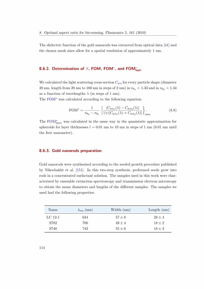
8. Optimal aspect ratio for bio-sensing, Plasmonics 5, 161 (2010)
The dielectric function of the gold nanorods was extracted from optical data [41] andthe chosen mesh sizes allow for a spatial resolution of approximately 1 nm.
8.6.2. Determination of S, FOM, FOM∗, and FOM∗layer
We calculated the light scattering cross-section Csca for every particle shape (diameter20 nm, length from 20 nm to 160 nm in steps of 2 nm) in nb1 = 1.33 and in nb2 = 1.34as a function of wavelengths λ (in steps of 1 nm).The FOM∗ was calculated according to the following equation:
FOM∗ = 1nb2 − nb1
[ |Csca1(λ)− Csca2(λ)|1/2 Csca1(λ) + Csca2(λ)]
max. (8.8)
The FOM∗layer was calculated in the same way in the quasistatic approximation forspheroids for layer thicknesses l = 0.01 nm to 10 nm in steps of 1 nm (0.01 nm untilthe first nanometer).
8.6.3. Gold nanorods preparation
Gold nanorods were synthesized according to the seeded growth procedure publishedby Nikoobakht et al. [151]. In this two-step synthesis, preformed seeds grow intorods in a concentrated surfactant solution. The samples used in this work were char-acterized by ensemble extinction spectroscopy and transmission electron microscopyto obtain the mean diameters and lengths of the different samples. The samples weused had the following properties:
Name λres (nm) Width (nm) Length (nm)
LC 12-1 634 57± 6 28± 4S702 700 49± 4 18± 2S740 743 55± 6 18± 3
114

8.6. Appendix - Methods
8.6.4. Single particle spectroscopy
To investigate the spectral shift by changes in the refractive index of the environmenton the single particle level, we dilute the nanorod suspensions 1:100 with distilledwater and rinse them for 5 min through a flat glass capillary connected to PETtubing. Subsequent rinsing of 1 M sodium chloride solution for 1 min can increasethe number of immobilized particles. Afterwards, the glass capillary is rinsed for atleast 15 min with distilled water (nb = 1.333) to remove as many of the molecules aspossible that were attached to the particle surface, and the scattering spectra of allparticles in the field of view recorded. After rinsing the glass capillary with glucosesolution (25 wt.% nb = 1.372) for 15 min, we again investigate the scattering spectraof the same particles and determine the quantities listed in Table 8.1.
115


9. PAPER: Highly sensitive plasmonicsilver nanorods
Arpad Jakab1, Yuriy Khalavka1, Jan Becker1, Andreas Trügler2,Christina Rosman1, Ulrich Hohenester2, and Carsten Sönnichsen1
1 MAINZ graduate school of excellence and Institute of Physical Chemistry, University of Mainz,Jakob-Welder-Weg 11, 55128 Mainz, Germany
2 Institut für Physik, Karl–Franzens–Universität Graz,Universitätsplatz 5, 8010 Graz, Austria
Published in: ACS Nano 5, 6880 (2011)
Abstract
We report experimental evidence of increased single particle plasmonic sensitivity ofsilver nanorods compared to gold rods with similar aspect ratios. We measured theplasmonic sensitivity of single gold and silver nanorods by monitoring the spectro-scopic change on changing the environment from water to 12.5% sugar solution. Wefind that silver has 1.2 to 2 times larger sensitivity than gold, in good agreementwith simulations based on the Boundary Element Method (BEM). Using the Drude-model of optical properties of metals together with the quasi-static-approximationfor localized surface plasmons we show that the reason for the higher sensitivity ofsilver is in the lower background polarizability of the inner shell electrons. However,the reversibility of the silver nanorod sensors, upon repeated cycles of environmentchanges, is much worse than of gold nanorods. Blocking parts of the illuminationlight by inserting a long-pass filter reduces this problem significantly.
117

9. Highly sensitive silver nanorods, submitted (2011)
9.1. Introduction
Sensor devices based on the refractive index sensitivity of surface plasmons haveemerged on the market in the last decade. Attempts to increase the sensitivity andreduce the sensor size focus on single particle based sensors and localized surfaceplasmons polaritons or particle plasmons [138,152,153]. As recently reported, singleparticle sensors can have a better sensitivity than propagating surface plasmon basedsensors [154].The spectral position of the localized surface plasmon is highly dependent on thedielectric properties of the surrounding medium [155]. For example, a change of thesurrounding refractive index of 0.02 from 1.333 to 1.353 results in a red shift of theresonance wavelength by 5.1 nm for a gold nanorod with an aspect ratio of 2.5. Foroptimal sensing of smallest dielectric changes (i.e. binding of small molecules), thespectral shift of the resonance wavelength upon changing the surrounding mediumhas to be maximized. Increasing the spectral shift can be achieved by various meth-ods like: optimizing the shape and size [140,156–158], inter-particle distance [124,159]or the material of the particle [158,160]. In recent times, efforts have been intensifiedto investigate silver nanoparticle sensitivity [161, 162]. In this work, we present ex-perimental results of single silver nanorod sensitivity revealing that silver nanorodshave a larger sensitivity than gold nanorods at the same resonance wavelength andthat – contrary to earlier predictions [139] – the background polarizability of thebound electrons strongly influences the sensitivity.
9.2. Synthesis
For our study, we form silver nanorods with various aspect ratios in solution adaptinga two-step “seeded growth” approach developed by Kitaev et al. [163] with smallmodifications in illumination and heating. In the first step, faceted silver “seeds”are produced under light illumination. We use a blue LED lamp (141 mW, peakmaximum at 459.5 nm, FWHM 20.53 nm) instead of the high power metal halidelamp used by Kitaev and co-workers. In the second step, the seeds are added to a“growth solution” where they develop into silver nanorods. We preheat the growthsolution in a consumer microwave at 90 W for 1 minute. Then AgNO3 is added
118

9.3. Plasmonic nanorod sensitivity
and the solution is placed into the microwave again for heating between 2 and 6minutes resulting in rods with increasing aspect ratio (AR). Two minutes of heatingresult in rods with an aspect ratio of 2.4± 0.8, four minutes yield an aspect ratio of2.9± 1.3, and six minutes an aspect ratio of 4.0± 1.6. (Fig. 9.1, top). We comparethe plasmonic sensitivity of those silver rods with gold nanorods produced by themethod of Nikoobakht et al. [151].
Figure 9.1.: Representative silver nanorod samples are shown as photographs andTEM images together with the corresponding ensemble extinction spectra (bot-tom). The samples correspond to: Ag-seeds and Ag-nanorods grown with 2, 4,and 6 minutes of heating time (from left to right). Their plasmon peak increasesfrom 485 nm to 633 nm, 776 nm, and 930 nm.
9.3. Plasmonic nanorod sensitivity
We observe the light scattering spectra of the single nanoparticles with a scanningdark-field setup [131] that allows for a rapid measurement of a large number ofimmobilized nanoparticles (Fig. 9.2 A). To measure the plasmon resonance shiftupon changes in the refractive index of the environment (single particle sensitivity),the nanoparticles are immobilized in a flat glass capillary or flow cell (the flow-cellpreparation is described in detail in the Methods section).
119

9. Highly sensitive silver nanorods, submitted (2011)
Figure 9.2.: (A) Experimental wet environment dark field setup designed for singlenanoparticle spectroscopy in various surrounding media. (B) Typical dark-fieldimage of the nanoparticles, the scale bar is 10 µm.
To immobilize nanoparticles in the flow cell, we add a suspension of nanoparticles inwater followed by a salt solution. The concentration of nanoparticles is adjusted bydilution to create a nanoparticle density in the field-of-view that allows the distinc-tion of single particles (Fig. 9.2 B); i.e. an average inter-particle distance of about10 µm. The addition of salt screens the surface charges that stabilize the nanopar-ticle suspension which leads to nonspecific adsorption of nanoparticles to the glasssurface of the flow cell. For gold nanorods, we used 0.1 M NaCl, for silver 0.1 MKNO3 because, as discussed later, chloride ions can cause structural changes to silvernanoparticles.Table 9.1 summarizes the size characteristics of the nanorods used for single parti-cle spectroscopic measurements. We used only silver nanorods from samples withmean longitudinal plasmon resonances of 633 nm and 776 nm (green and red curvesin Fig. 9.1). Those silver nanorods had a mean width of about 55-60 nm and as-pect ratios of 2.4:1 and 2.9:1, respectively. In comparison, the gold nanorods weresmaller with a width of 11-28 nm but with comparable aspect ratios. More detailsabout the nanoparticle size distribution are presented in Fig. 9.5 and Table 9.2 inthe Supporting Information 9.9.
120

9.4. Sensitivity measurements
Nanorod Material Longitudinalensemble peak
Width Aspect Ratio(length/width)
Ag 633 nm 55 ± 10 nm 2.4 ± 0.8Ag 776 nm 59 ± 14 nm 2.9 ± 1.3Au 634 nm 28 ± 4 nm 2.0 ± 0.1Au 702 nm 18 ± 2 nm 2.7 ± 0.1Au 743 nm 18 ± 3 nm 3.1 ± 0.2Au 816 nm 11 ± 2 nm 4.1 ± 0.1
Table 9.1.: Properties of the silver and gold nanorods used in our study (sizes fromTEM images).
9.4. Sensitivity measurements
The plasmon sensitivity quantifies the dependence of the plasmon resonance wave-length or frequency on changes in the dielectric properties of the surrounding medium.Sensitivity S (in wavelength units) is therefore defined by S = dλres/dnb, where λresis the plasmon resonance wavelength and nb is the refractive index of the surround-ing medium. There are more elaborate measures to quantify the sensor qualityof nanoparticles taking into account more realistic sensor concepts, for exampleFOM [144, 164], FOM∗, [156] MFOM [165]. All of these quantities depend on theplasmon sensitivity. Here we focus on the sensitivity in wavelength units and referto this term simply as ’sensitivity’.We determined the plasmonic sensitivity experimentally by recording spectra of sin-gle immobilized nanoparticles in the initial environment (pure water, n1 = 1.3330),then immersed in 12.5% sucrose solution (n2 = 1.3454), and at the end again inwater. The resulting experimental results are shown as red crosses (gold nanorods)and blue stars (silver nanorods) in Fig. 9.3 (top panel). The red and blue continuouslines are trend-lines of the datasets. The experimentally obtained trend-lines quali-tatively follow the trend simulated with the BEM [83] (dashed lines) but are lowerthan the simulation. However, the simulation was performed with a homogenousmedium around the particles whereas in the experiment, the particles are attachedto a glass substrate reducing the influence of the change in medium. The fact thatthe experimental silver trend shows a stronger deviation from simulations than thegold nanorods might be caused by additional damping of the plasmon resonance dueto their penta-twinned crystal structure [166].
121

9. Highly sensitive silver nanorods, submitted (2011)
Figure 9.3.: Top: Single particle sensitivity data plotted for each particle bothfor silver and gold. The continuous blue and red lines are the averages of theexperimental data of silver and gold, respectively, the dashed lines are obtainedin BEM simulations. Bottom: the experimentally obtained (continuous line) andBEM-simulated (dashed line) sensitivity enhancement (SAg/SAu) of silver nanorodsin relation to gold nanorods.
The average silver sensitivity is larger than the gold sensitivity. The sensitivity ofsilver nanorods reaches values above 400 nm/RIU which is, up to now, the largest valuefor rod-like objects in this wavelength range [157]. Especially in the wavelength rangeof 600 to 700 nm, where gold has only a sensitivity of 150 - 270 nm/RIU, silver performsbetter with sensitivities of above 300 nm/RIU. We believe that the scattering of thedata points around the trend lines is primarily caused by the varying thicknesses ofthe surface stabilizing layer (Ag: PVP, Au: CTAB) around the particles.To directly compare the sensitivity of gold and silver, we show the ratio of theirsensitivity (the sensitivity enhancement of silver compared to gold SAg/SAu) in thebottom plot of Fig. 9.3, both for the experimental data and the simulation. Theexperiment and simulation agree well in this diagram, the substrate effect effectivelycancels out. At shorter wavelengths, around 610 nm, the enhancement reaches afactor of two, at longer wavelengths the enhancement drops to a value between 1.1and 1.2.
122

9.5. Discussion and Model
9.5. Discussion and Model
To understand the origin of the higher plasmonic sensitivity of silver nanorods com-pared to gold nanorods, it is sufficient to use the quasi-static approximation to cal-culate the scattering cross section together with a simple Drude-type model for thedielectric function for gold and silver. Within those two approximations, the sensi-tivity S at a given resonance wavelength λ is given by the following equation (seeSupporting Information 9.9 for details):
S(λ) = λ
nb
(1−
λ2p
λ2n2∞
), (9.1)
where λp = 2πc/ωp is the bulk plasmon wavelength (λp = 136 nm for gold and sil-ver), n∞ = √ε∞ is the background refractive index, the square root of the back-ground dielectric constant, originating from the polarizability of the bound electrons(ε∞,Au = 9.84 for gold and ε∞,Ag = 3.7 for silver correspond to n∞,Au = 3.1 andn∞,Ag = 1.9, respectively), and nb is the refractive index of the surrounding medium.The equation above reveals that, contrary to earlier reports [139], the sensitivity de-pends on the material through the strong difference in the background polarizabilityε∞ of gold and silver (the sensitivity decreases with increasing ε∞ or n∞ ). Despitethe simplifications of the quasi-static approach and the Drude model for the dielec-tric function, the equation above predicts the sensitivity of nanorods remarkably well(Fig. 9.6 in the Supporting Information compares the sensitivity calculated with theBEM with tabulated dielectric values for gold and silver, to the sensitivity calcu-lated with the simple model above). We have not used any assumptions about thephysical dimensions and shape of the particle during the derivation of the equationabove. The sensitivity of a plasmonic nanoparticle at a given wavelength is thereforeindependent from its shape and size as long the conditions for the approximationsare valid (e.g. no retardation effects, no interband damping).
123

9. Highly sensitive silver nanorods, submitted (2011)
9.6. Sensing Reversibility
Whereas sensitivity alone seems to favor silver over gold, another important aspect forsensors is the sensing reversibility upon repeated changes of the environment. Giventhe fact that silver is less noble than gold, we carefully checked the reversibility.For this purpose, our measurements always went back to the initial environmentat the end and we recorded the difference in resonance wavelength between initialand final resonance wavelength, a quantity we call the sensing cycle shift. For areliable sensor, the mean sensing cycle shift should remain close to the experimentaluncertainty (±0.5 nm) and we disregarded all particles that did not show a fullreversibility in the datasets for estimating particle sensitivity (reversibility withinone standard deviation). Halide ions (Cl− and especially Br−) induce a reshaping ofsilver nanoparticles above a threshold concentration of ~10−8 M, so we took care toavoid any use of those ions [167, 168]. Generally, we found that even without halideions present, silver nanoparticles showed much worse reversibility performance thangold. We suspected a light induced process so we measured the reversibility withdifferent filters in the light path.In Fig. 9.4 we show the sensing cycle shift of single nanorods plotted as a cumulativedistribution probability (an integrated histogram that allows an easy visualizationof the mean value) measured under different illumination conditions where each dotcorresponds to the sensitivity cycle shift of a single particle. The sensing cycle shift isdecreasing with increasing cut-off wavelength of the long pass filter. The mechanismof this light-induced irreversible shift remains unclear and is probably a combinationof heating and photochemical processes. The shift has nothing to do with changingthe environment as we checked in experiments that show a red shift of nanoparticlesmonitored continuously in water (Fig. 9.9 in the Supporting Information 9.9). Ourexperiments indicate that a sufficiently high cut-off filter allows the use of silvernanoparticles for sensing in environments without halide ions.
9.7. Conclusion
We have presented experimental results of silver nanorod sensitivity and comparedthem to results found for gold nanorods. Silver nanorods have up to two times
124

9.8. Methods
Figure 9.4.: Cumulative distribution of single nanoparticle resonance wavelengthshifts after one sensing measurement cycle (the sensing cycle shift). The continuouslines are Gaussian fits, the arrow indicates the mean cycle shift. Left graph: (1)Au rods with 610 nm long pass (LP) filter (2) Au rods without LP filter. Rightgraph: (3) Ag rods with 610 nm LP filter, (4) Ag rods with 530 nm LP filter (5)Ag rods without LP filter. Inset at bottom right: definition of sensing cycle shift∆λres in the cycle n1 → n2 → n1.
larger sensitivity than gold nanorods in the spectral range of 600 to 700 nm. Inthe region of 700 to 900 nm, the sensitivity is still about 10 to 20% higher. Fromsimple theoretical arguments (Drude’s model of optical properties of metals and thequasi-static-approximation), we could identify the lower background polarizability ofsilver compared to gold as the main reason. The reversibility of silver nanorod basedsensors is, generally, worse than gold nanorod based sensors, but adding a 610 nmcut-off long-pass filter in the light path, resulted in a reasonably reversible sensor forboth cases.
9.8. Methods
9.8.1. Reagents
Silver nitrate (99%), sodium citrate tribasic dihydrate (Aldrich 99%), polyvinylpyrroli-done (PVP, Mw 40K), sodium borohydride (99%, Aldrich), L-arginine (98%, Aldrich)were used as received. Millipore deionized water was used as solvent.
125

9. Highly sensitive silver nanorods, submitted (2011)
9.8.2. Synthesis of Silver Nanorods
Silver nanorods were synthesized following mainly the procedure developed by Kitaevet al. [163]. Decahedral Ag nanoparticles were used as seeds. For their synthesis, aprecursor solution of silver nanoparticles was first prepared using a mixture of 1.000mL of 0.05 M sodium citrate, 0.060 mL of 0.05 M PVP, 0.100 mL of 0.005 M L-arginine, 0.400 mL of 0.005 M AgNO3 and 14.0 mL of deionized water in a 20 mLvial and then reduced by adding 0.160 mL of 0.10 M NaBH4. The resulting yellowsolution was stirred for several minutes. To produce decahedra, a blue diode arraylamp with λmax 460 nm with an exposure time of 10 hours was used (spectrum inthe Supporting Information 9.9). In the next step, 2 mL of the freshly prepareddecahedral Ag seed solution were centrifuged to replace the supernatant with 1.0 mLof pure deionized water.Having prepared the decahedra seed solution, 1 mL of the purified decahedra solution,2.0 mL of water, 0.400 mL of 0.05 M sodium citrate, and 0.066 mL of 0.05 M PVPwere heated to 95 in a 20 mL vial in microwave oven at 90 W power. Aftertemperature equilibration, 0.400 mL of silver nitrate (0.005 M) were added at onceto produce rods with an aspect ratio up to 4-5 in high yield in 2-6 minutes of thereaction under 90 W microwave power.
9.8.3. Characterization
Transmission electron microscopy was performed using FEI Tecnai F30 and PhillipsEM-420 microscopes. Nanoparticle solutions were deposited on a carbon-coated For-mvar grid (Plano). Operating voltage was varied from 120-300 kV. The average sizeand standard deviation were determined from TEM images by averaging diametersof about 100 particles. Ensemble optical spectra were acquired with Ocean OpticsUSB 2000 spectrometer.
Single Particle Microscopy
The single particle spectroscopy was performed with a self-build microscopy setupemploying a 2D piezo scanner. The setup shown in Fig. 9.2 consists of a position-ing stage (PI P-542.2CD Nanopositioning and Scanning Stage), microscope optics,an imaging spectrometer (Princeton Instruments/ACTON SpectraPro 2300), and a
126

9.9. Supporting Material
CCD camera (Princeton Instruments Pixis 400B). During a spectral scan, the sampleis moved in steps of 1 µm along the x-axis. At each step, the spectrum of the particlesin the center column is taken. The scan window width is adjusted to the step size toensure gapless coverage of the scanned area.
Flow Cell
The glass capillary (Vitrotube W5010-100 by Vitrocom) is initially UV-irradiatedfor 15 minutes and left for another 15 minutes in the reactive atmosphere, then weattach thin polyethylene tubing using epoxy glue to construct the flow cell system.The flow cell is purged with 1% Helmanex solution for 24 hours, and finally cleanedwith hot deionized water for 1 hour.
9.9. Supporting Material
Figure 9.5.: Histogram of width (red) and length (blue) for Ag-rod samples widthdifferent average length (from TEM images).
Sample No. of Part. Width (nm) STD (nm) Length (nm) STD (nm)
Short Rods 88 55 10 124 16Med. Rods 98 59 13 159 27Large Rods 459 58 12 212 39
Table 9.2.: Dimensional characterization of the silver nanoparticles that were usedfor single particle sensitivity measurements. The relative standard deviation of thewidths is slightly larger (20%) than of the lengths (15%).
127

9. Highly sensitive silver nanorods, submitted (2011)
Figure 9.6.: Comparison of sensitivitiesobtained by BEM simulation (dashedlines) and the free electron Drude-Modelof Eq. (9.7) below (dotted lines). Forreference, we have also included the ex-perimentally obtained sensitivity data(continuous lines). Despite the simplifi-cations used in the free electron Drude-Model, it follows the simulated curve re-markably well.
Figure 9.7.: Example of a white lightscattering spectrum of a single silvernanorod. For unpolarized excitation,both the long axis (or longitudinal) andthe short axis (or transversal) plasmonresonances are visible.
Figure 9.8.: The spectrum of the blueLED lamp used to grow silver seeds.
Figure 9.9.: Spectral stability ofnanoparticles measured under identicalconditions as during sensitivity mea-surements, except that here the sur-rounding medium was always water.The graph shows the influence of thelong pass filter on the spectral stabilityof Au and Ag nanoparticles by plottingthe cumulative probability (integratedhistogram) of the spectral shift ∆λres 1:Au with 610 nm long pass filter, 2: Agwith 610 nm long pass filter, 3: Au with-out long pass filter, 4: Ag without longpass filter. The spectral stability of goldis better (smaller average shift) than ofsilver. We assume that some activationenergy related photochemical process isinducing an irreversible reshaping of thenanoparticle.
128

9.9. Supporting Material
9.9.1. Derivation of the plasmonic sensitivity equation
Within the quasi-static approximation (i.e. for particle dimensions much smallerthan the light wavelength), the scattering cross-section of a particle is proportionalto the square of the modulus of the polarizability: Csca ∝ |α|2. The polarizability isgiven by:
α = V
4πεr − 1
1 + L (εr − 1) . (9.2)
Where εr = ε(ω)/εr is the relative dielectric function of the particle ε(ω) to the em-bedding medium εb, L is a geometric depolarization form factor that is well approx-imated by L = (1 + AR)−1.6 for rods with aspect ratio (AR) between 1 to 8. Theplasmon resonance occurs at the frequency where the denominator becomes zero, i.e.1 + L(εr − 1) = 0.Within the Drude model, the real part of the metals dielectric function is given by
<e(ε) = ε∞ −ω2p
ω2 + γ2 ≈ ε∞ −ω2p
ω2 (9.3)
where γ is the free electron damping, which is negligible for gold and silver in the vis-ible spectral range, ωp is the plasma frequency (ωp = 9.1 eV for both gold and silver),and ε∞ the background polarizability arising from the bound electrons (ε∞,Au = 9.84for gold and ε∞,Ag = 3.7 for silver). The lower value for background polarizabilityof silver reflects the deeper lying d-band with an offset to the Fermi-energy of 4 eVcompared to 2 eV for gold.Using Eq. (9.3) as the frequency dependent dielectric function for the nanoparti-cle and inserting it into the resonance condition (denominator in Eq. (9.2) is zero)1+L(εr−1) = 0, we can obtain the resonance wavelength λres = 2πc/ωres. We replaceεb for practical purposes with the refractive index of the surrounding medium nb
= ε1/2b
λres = λp
√ε∞ + n2
b
( 1L− 1
), (9.4)
where λp = 2πc/ωp = 136 nm is the bulk plasmon wavelength with c, the speed oflight in vacuum.Since the sensitivity is defined by the change of the resonance wavelength λres with
129

9. Highly sensitive silver nanorods, submitted (2011)
the surrounding refractive index nb, we arrive at the equation for the sensitivity:
S = d
dnbλres = λp nb√
n2∞
(L
1−L
)2+ n2
b
(L
1−L
)2, (9.5)
where n∞ = ε1/2∞ is the background refractive index. To be able to directly compare
the experimental data to the results of the analytic expression in Eq. (9.5), we need toexpress the sensitivity as function of the resonance wavelength. Thus we use Eq. (9.4)and rearrange it to express L/1−L as function of n∞, nb, λp and λres we get:
(L
1− L
)= n2
bλ2
res/λ2p − n2
∞. (9.6)
Inserting the right side of Eq. (9.6) into Eq. (9.5) and writing λ for λres we get:
S(λ) = λ
nb
(1−
λ2p
λ2n2∞
). (9.7)
9.10. Acknowledgments
We acknowledge financial support by the DFG through the Emmy Noether Program(SO712/1-3) and the Graz Advanced School of Science (NAWI GASS). Arpad Jakaband Yuriy Khalavka were recipients of the MAINZ graduate school of excellencefellowship through funding of the Excellence Initiative (DFG/GSC 266).
130

10. PAPER: Superresolution Moirémapping of particle plasmon modes
Daniel Koller, Ulrich Hohenester, Andreas Hohenau, Harald Ditlbacher, Frank Reil,Nicole Galler, Franz Aussenegg, Alfred Leitner, Andreas Trügler,
and Joachim Krenn
Institute of Physics and Erwin Schrödinger Institute for Nanoscale Research,Karl–Franzens–University, 8010 Graz, Austria
Published in: Phys. Rev. Lett. 104, 143901 (2010)
Abstract
The spontaneous emission rate of a fluorophore provides a direct probe of the photoniclocal density of states at the fluorophore position. Here we exploit this capabilityto map the plasmonic modes of gold nanoparticles by imaging the fluorescence in-tensity in combined regular arrays of identical gold and fluorophore-doped polymernanoparticles. By varying the distance between gold and polymer particles across thearray, the fluorophore emission generates an optical Moiré pattern corresponding toa magnified spatial map of the plasmonic mode, which can be directly imaged withan optical microscope. Our results are corroborated by supplementary theoreticalmodel calculations.
131

10. Superresolution Moiré mapping, PRL 104, 143901 (2010)
Surface plasmons enable the nanoscale localization of light and provide an effec-tive means to control the excitation and emission properties of quantum systems.These appealing properties have triggered a large variety of recent research anddevelopment in fields as diverse as data storage [13], quantum optics [16, 17], op-toelectronics [18, 19], photovoltaics [20], sensors [7], and cancer research [6]. Witha demand for ever increasing miniaturization and integration densities for many ofthese applications, the spatially and spectroscopically resolved characterization ofplasmonic nanostructures has to be improved as well. Recent developments in thisdirection include progress in near field scanning microscopy [169, 170], two-photonluminescence based imaging [171] and spatially resolved electron energy loss spec-troscopy [108,172].
In this Letter, we demonstrate a straightforward method to image plasmonic modeswith subwavelength resolution, and spectral and polarization discrimination. Tothis end, we arrange identical copies of plasmonic gold nanoparticles in a 2D array,and superpose this pattern with a geometrically incommensurable 2D array of dyedoped polymer nanoparticles. The dye emission is spectrally tuned to the plasmonicresonance and thus serves as a sensitive probe of the plasmonic mode density [173]. Asthe distance between gold and polymer particles varies across the array, a microscaleMoiré pattern is generated by the dye emission that corresponds to a magnifiedspatial map of the plasmonic mode.
Metal structures sustaining surface plasmons can substantially alter the excitationand emission rates of a nearby quantum system as, e.g., a fluorophore [174, 175].While excitation rates can be increased by the strong local plasmonic fields, themolecular emission rate is boosted in response to the high plasmonic LDOS accordingto Fermi’s Golden Rule [4]. It has been shown recently that fluorophores with a largeStokes shift allow to access the emission channel modification only [173], therebyenabling direct measurements of the plasmonic LDOS. Here, we apply this approachto the high-resolution mapping of the plasmonic modes of lithographically tailoredgold nanoparticles with resonance wavelengths in the red spectral range [black linein Fig. 10.1(a)].
Square gold nanoparticles (side length 100 nm, height 50nm) were fabricated over anarea of 100µm × 100µm, arranged in a regular square array with a grating constant
132

Flu
ore
scence
inte
nsity (
arb
.u.)
a b
dc
G + dGG
MNPPtTFPPin SU-8
Wavelength (nm)
300 nm0.0
0.2
0.4
0.6
0.8
1.0
550 600 650 700 750 8000.0
0.2
0.4
0.6
0.8
1.0
No
rma
lize
d e
xtin
ctio
n
No
rma
lize
d in
ten
sity
Wavelength (nm)
Figure 10.1.: (Color online) Principles of fluorescence Moiré mapping of goldnanoparticles. (a) Normalized plasmonic extinction (black curve) and photolu-minescence spectra (red curve) of gold and SU8/PtTFPP nanoparticle arrays, re-spectively. (b) Scanning electron micrographs of (upper row) arrays of gold andSU8/PtTFPP nanoparticles and (lower row) a combined array of both nanoparticletypes. (c) Photoluminescence spectra acquired from heterogeneous arrays of goldand SU8/PtTFPP nanoparticles. The relative mutual position of the nanoparticleswithin the array is shown in the insets for one particle pair. (d) Schematic sketchof distance variations of both types of nanoparticles within the combined arraysused for Moiré imaging, due to two different grating constants G and G+dG.
of G = 400nm on indium-tin-oxide covered glass substrates by an electron beamlithography lift-off process relying on the positive resist poly(methyl methacrylate).We found the gold nanoparticles to be geometrically virtually identical throughoutthe array [upper left image in Fig. 10.1(b)]. Individual features in particle geometrydeviating from the mean shape can amount to ±3 nm, limiting the achievable spatialresolution, while variations of the plasmonic resonance are negligible. As the fluo-rophore we chose a platinum porphyrin (PtTFPP) with an absorption band in theblue spectral range and an emission band centered at a wavelength of 650 nm. In
133

10. Superresolution Moiré mapping, PRL 104, 143901 (2010)
this case the plasmonic influence on the absorption rate is negligible [173]. PtTFPPwas mixed at a concentration of 49.5 g/l into the negative tone resist SU-8-3010(MicroChem Corp.) which was diluted before with SU8-2000-thinner (MicroChemCorp.) at a ratio of 1:20. This concentration was found to yield homogeneouslydispersed molecules with easily detectable fluorescence signal levels which are notstrongly affected upon electron irradiation.Electron beam exposure of a 60 nm thick PtTFPP doped SU8 film deposited by spincoating on indium-tin-oxide covered glass substrates yielded nanoparticles with a di-ameter of 40 nm and a height of 60nm, containing about 2000 PtTFPP moleculeseach. Again, the particles were arranged in a square array with G = 400nm over anarea of 100µm × 100µm [upper right image in Fig. 10.1(b)]. A photoluminescencespectrum of this array is shown by the red line in Fig. 10.1(a).
By combining both lithography schemes to an aligned two-step writing process, wefabricated heterogeneous arrays of gold and SU8/PtTFPP nanoparticles, as shownin the lower row of Fig. 10.1(b). SU8/PtTFPP particles positioned directly on goldparticles showed about 2 times larger volumes as compared to particles sitting di-rectly on the substrate which is most likely due to increased electron backscatteringduring the lithographic exposure process. We note that quenching in the case of SU8particles in direct contact with a gold particle does not play a major role as onlya few molecules are within quenching distance [174] due to the height of the SU8particle.The measured integral fluorescence intensity from the heterogeneous arrays dependson the mutual distance of gold and SU8/PtTFPP nanoparticles, thus giving a mea-sure of the LDOS at the position of the molecules [Fig. 10.1(c)]. While the presenceof the SU8 particle in principle causes a modification of the dielectric environmentof the gold particle, measurements on arrays with different mutual distances of bothtypes of particles show that no significant spectral modification of the plasmonicband takes place.
We next increased the grating constant for the SU8/PtTFPP array by dG = 2nm to402 nm, while maintaining G = 400nm for the gold particle array. The distance be-tween SU8/PtTFPP and gold nanoparticles forming neighboring pairs is thus shiftedby dG when moving from one pair to the next. The fluorescence emission intensitychanges accordingly, spatially sampling the plasmonic LDOS [Fig. 10.1(d)]. Conse-
134

quently, the fluorescence intensity distribution within the array as directly observablewith a microscope is an image representing the LDOS of the (virtually identical) goldparticles, with a magnification factor of G/dG = 200. The achievable spatial resolutionis determined by the smallest possible step size in the lithographic process, and isnot limited by diffraction.
The fluorescence measurements were performed with a conventional optical micro-scope equipped with a mercury lamp as the illumination source, band-pass filteredto 365± 20 nm. A 20×, numerical aperture = 0.5 microscope objective was used forboth unpolarized sample illumination and fluorescence imaging onto a charge coupleddevice camera after passing a 515 nm high-pass filter.
An exemplary fluorescence image of a square gold nanoparticle under unpolarizedillumination is shown in Fig. 10.2(a). The variation of the mutual distance betweengold and SU8/PtTFPP nanoparticles is illustrated in the insets for five positionswithin the array. We observe a well defined square pattern in the fluorescence image,corresponding to the particle geometry. The ratio of the full-width-at-half-maximumof the fluorescence pattern [as defined in the cross-cut in Fig. 10.2(b)] and the par-ticle size is 210. While a comparison of the dimensions of the geometrical particlesize and the plasmonic mode pattern is in principle meaningless, the found value isnevertheless close to the magnification value of 200, as defined above, due to thestrong localization of the plasmonic field to the particle surface. The curvature ofthe particle corners of about 5 nm is very well reproduced in the image, emphasizingnanoscale spatial resolution.
A key advantage of our method is the direct access to polarization-dependent andspectroscopic information by simply introducing a polarizer and spectral filters intothe optical detection branch. Therefore additional filters were used for spectral selec-tivity (band pass 650±10 nm, 670±10nm and long pass ≥ 720nm), and a polarizer infront of the camera allowed to analyze polarization dependencies. Fig. 10.3(a) showsa series of images of the square gold nanoparticle as in Fig. 10.2(a) but with bothpolarized and spectrally filtered detection, indicated to the left and on top of theimage, respectively. Depending on polarization the mode pattern appears rotatedby 90, as expected for a dipolar excitation. The spectrally filtered images revealsubtle changes when moving the spectral window over the plasmonic resonance at
135

10. Superresolution Moiré mapping, PRL 104, 143901 (2010)
Figure 10.2.: (Color online) Fluorescence Moiré mapping of a gold nanoparticle.(a) Image of a square gold nanoparticle (side length 100 nm, height 50nm) withinan 100µm × 100µm large array containing 250× 250 particles. Unpolarized exci-tation at wavelengths of 365± 20nm and detection through a high-pass filter witha cut-off wavelength of 515nm were applied. The scanning electron micrographs inthe insets illustrate the variable distance between gold and SU8/PtTFPP nanopar-ticles, according to their position within the array. (b) Cross-cut along the dashedline in (a) revealing a ratio of Moiré image size and geometrical particle size (inset)of 210.
670 nm [Fig. 10.1(a)]. Both to the short-wavelength side of the resonance (band-passfilter 650 ± 10 nm) and on-resonance (band-pass filter 670 ± 10nm) the plasmonicmode appears strongly localized to the particle while on the long-wavelength side(long-pass filter ≥ 720 nm) the dipolar mode pattern extends further away from theparticle. In addition, we observe bright and dark areas in between the nanoparticlescorresponding to areas of enhanced and supressed LDOS, to be discussed furtherbelow. Areas of increased LDOS are particularly strong for the wavelength band650± 10 nm, according to a radiating grating order at near-grazing angles [176]. Wenote that the intensity levels in the images are normalized to optimum contrast asmolecular bleaching taking place during image acquisition (corresponding to about5% intensity decrease) makes the comparison of absolute signal levels impossible.
For closer analysis of the experimental data we performed simulations based on theBoundary Element Method (BEM) [56, 82], which does not introduce any fittingparameters. The dielectric function of gold was extracted from optical data [41]. Asthe presence of a substrate was not taken into account in the calculations we assumeda homogeneous medium with a refractive index of 1.5. The geometry of the modeled
136

Figure 10.3.: (Color online) Polarization and wavelength dependence of the plasmonmode of a square gold nanoparticle. Polarization directions and wavelength rangesare given to the left and on top, respectively. (a) Experimental images for (upperrow) horizontal and (lower row) vertical polarization and spectral ranges (left toright) 650 ± 10 nm, 670 ± 10 nm and ≥ 720 nm. The color-encoded intensities ineach image are normalized to optimum contrast and thus cannot be compared fromone to another. (b) BEM simulations for the polarization directions indicated tothe left and for discrete wavelengths of (from left to right) 650nm, 670nm and720 nm.
gold nanoparticles (100 × 100 × 50 nm3 for the square particles and 100 × 300 × 50nm3 for the nanorods) were chosen to match the measured extinction spectra. Toaccount for the regular particle arrangement we simulate an ensemble of four goldnanoparticles arranged according to the experimental conditions, i.e., G = 400 nm.We model the molecules as dipole resonators, with moment d, which are situated atpositions r. To account for the off-resonant excitation, we assume that the moleculeis initially excited and subsequently decays, either through electromagnetic coupling
137

10. Superresolution Moiré mapping, PRL 104, 143901 (2010)
or via intra-molecular channels. The electromagnetic decay rate γem(d,r,ω) at agiven photon energy ~ω is obtained from the imaginary part of the dyadic Greenfunction [4], and the intra-molecular decay rate γmol is related to the quantum yieldof the isolated molecule, which we estimate to be about ten percent [177]. With γΩ,`
raddenoting the differential cross section for light emission into a sphere segment Ω,which corresponds to the experimental conditions, and ` being the polarization, wecan express the measured luminescence intensity, governed by the plasmonic LDOS,as
Moiré luminescence intensity
IΩ,`lum(R0, ω) ∝
⟨γΩ,`
rad(d, r, ω)γem(d, r, ω) + γmol
⟩. (10.1)
This quantity describes the probability that an excited molecule emits a photon intothe direction of the photodetector. The brackets denote an ensemble average overthe dipole orientations and positions r within the SU8 nanoparticle, centered atR0. We assume a homogeneous distribution of randomly oriented dipole momentswithin a volume corresponding to the SU8 nanoparticle. The larger volume of theSU8/PtTFPP particles on top of the gold particles has been taken into accountaccordingly.
Fig. 10.3(b) shows maps calculated with Eq. (10.1) which directly correspond to theexperimental images in Fig. 10.3(a). We emphasize that the simulation shows a singleparticle while in the experiment a magnified image including many nanoparticles isobserved. From the comparison of the according images in Fig. 10.3(a) and (b)the agreement of experiment and simulation is evident, which we take as directproof of the LDOS imaging properties of our system. In particular, the evolutionof the spatial profile of the LDOS pattern as a function of observation wavelengthis well reproduced. We found that the dark spots in between the particles occurat the positions where the electric field of the induced surface plasmon interferesdestructively with the driving dipole of the molecule. Due to the phase difference
138

between driving dipole and driven molecule, the composite system has a smallereffective dipole, thus corresponding to a smaller LDOS.
Figure 10.4.: Polarization and wavelength dependence of the plasmon mode of agold nanorod. (a) Experimental images as in Fig. 10.3, but for a gold nanorodwith 300 nm length, 100 nm width and 50 nm height. The intensities in each imageare normalized to optimum contrast and thus cannot be compared from one toanother. (b) BEM simulations for the polarization directions indicated to the leftand for discrete wavelengths of (from left to right) 650 nm, 670 nm and 720nm.
Next, we investigate gold nanorods with a cross section diameter and length of 100and 300 nm, respectively, and a height of 50nm, arranged in a square pattern with G= 400nm. The dipolar resonances for excitation light polarizations along the shortand long nanorod axes lie at a wavelength of 660 nm and in the infrared spectralrange, respectively. The relative positions of nanorods and SU8/PtTFPP nanopar-ticles throughout the array were chosen such that two entire and part of two furthernanorods appear in the images. Fig. 10.4(a) shows the experimental images, for ex-perimental parameters as in Fig. 10.3. For polarization along the short nanorod axis
139

10. Superresolution Moiré mapping, PRL 104, 143901 (2010)
we again find strongly localized mode patterns for the short-wavelength side of theresonance and on-resonance. The corresponding calculations in Fig. 10.4(b) revealthese patterns as due to excitations of a dipolar plasmonic mode along the shortaxis of the nanorod. For the off-resonant case (wavelengths ≥ 720 nm) less confinedfields are observed, again corresponding to the simulation. Choosing the polarizationdirection along the nanorod axis we find that the fluorescence signal becomes moreconfined to the center of the nanorod when increasing the observation wavelengths.The comparision with the simulations in Fig. 10.4(b) reveals the likely explanationfor this effect. For wavelenghts ≥ 720 nm a non-resonant excitation of the dipolarresonance (in the infrared spectral range) dominates, giving rise to a rather localizedmode pattern. For a wavelength of 650 nm, however, the quadrupolar mode prevails,corresponding to a spatially more extented mode. Again, the fluorescence maximain between the nanorods can be explained due to the grating effect.
The superresolution access to plasmonic modes by fluorescence Moiré mapping asdiscussed here can in principle be extented to any nanooptical system. While SU8/PtTFPP nanoparticles have been found to be a particularly stable probe for theLDOS, probing other wavelength ranges on the basis of different fluorophores isstraightforward. The challenge of well-controlled pattern fabrication could possiblybe met by nanoimprinting based processes. Besides LDOS mapping and nanoparti-cle/quantum emitter studies, such systems could be useful for applications in sensorsor wavelength and polarization encoded security features.
The GASS of NAWI Graz is acknowledged for financial support.
140

11. PAPER: High-resolution surfaceplasmon imaging of goldnanoparticles by Energy FilteredTransmission Electron Microscopy
Bernhard Schaffer1,2,3, Ulrich Hohenester4, Andreas Trügler4, and Ferdinand Hofer1
1 Institute for Electron Microscopy and Fine Structure Research, Graz University of Technology, 8010 Graz2 SuperSTEM Laboratory, STFC Daresbury, Keckwick Lane, WA4 4AD, Warrington, United Kingdom3 Department of Physics and Astronomy, University of Glasgow, G12 8QQ, Glasgow, United Kingdom
4 Institut für Physik, Karl–Franzens–Universität Graz, Universitätsplatz 5, 8010 Graz, Austria
Published in: Phys. Rev. B 79, 041401(R) (2009)
Abstract
We demonstrate the imaging capabilities of energy-filtered transmission electron mi-croscopy at high energy resolution in the low energy loss region, reporting the firstdirect image of a surface plasmon of an elongated gold nanoparticle at energies around1 eV. Using complimentary model calculations performed within the boundary ele-ment method approach we can assign the observed results to the plasmon eigenmodesof the metallic nanoparticle.
141

11. High-resolution plasmon imaging, PRB 79, 041401(R) (2009)
11.1. Introduction
Plasmonics is an emerging field with numerous applications [5, 178], ranging fromoptical data processing [14, 15] over negative-refraction materials [10, 11] to bio-sensors [8,9]. Surface plasmons, the workhorse of plasmonics, allow to bridge betweenthe micro- and nanometer length scales of conventional optics and nano-devices.This is achieved by binding or converting light to coherent electron charge oscilla-tions, confined to the surface of metallic nanostructures. When optical emitters,such as molecules or quantum dots, are placed in the vicinity of metallic nanoparti-cles, they couple strongly to the evanescent fields of the surface plasmons, and thelight-matter coupling becomes significantly enhanced. This is exploited in surfaceenhanced Raman scattering [179] or surface enhanced fluorescence [180], as well asin single-plasmon generation [16].
The electromagnetic enhancement is particularly strong at the so-called “hot spots”,with typical sizes of a few nanometers, which are usually located in the gaps betweentwo nanoparticles or at the sharp edges of single particles. While enhancement fac-tors of several orders of magnitude are predicted [4], the analysis of the experimentaldata is often cumbersome and controversial due to the limited spatial resolution pro-vided by optical far- and nearfield techniques, as well as due to the uncertaintiesregarding the precise location of the optical emitters. An alternative experimentaltechnique, which allows to bypass these difficulties, is EELS in combination withscanning transmission electron microscopy (STEM) [108]. Here, a high-energy elec-tron beam, with a transversal extension on the sub-nanometer scale, passes in thevicinity or through the nanoparticle, and some electrons lose energy through plasmonexcitations, which are subsequently monitored. By raster scanning the beam over themetallic nanoparticle, one obtains information about the photonic local density ofstates of the metallic nanoparticles [107,108,181]. The spatial resolution of the mapsis limited to the nanometer range by delocalization of the inelastic scattering [182].
The drawbacks of the EELS technique have so far been the energy cutoff in the low-energy regime and the limited spatial resolution in large-area mappings. On the onehand, the so-called zero-loss peak (ZLP) of the electron beam usually masks the low-energy part of the spectrum. This hinders the direct observation of surface plasmonsin the red and infra-red regime, which is particularly appealing for (bio)sensors or
142

11.2. Experiment
applications at the telecom wavelengths. On the other hand, as STEM EELS dataare sequentially acquired point-by-point, the sampling of the spatial dimensions islimited by keeping the total acquisition time low, which leads to usually rather coarsemaps.
In this Letter we show that EFTEM as an alternative acquisition technique enables usto directly image surface plasmons at low energies. As a parallel imaging technique,which gathers images using scattered electrons of a specific energy loss range only, itachieves high spatial sampling easily and fast, while providing the same informationcontent as STEM EELS [183, 184]. The energy resolution of the EFTEM techniqueis typically in the range of a few eV, but can be pushed to the sub-eV range if a smallenergy-filtering slit width and appropriate data correction schemes are used [185].This enabled us to directly monitor surface plasmons at energies around or below1 eV without employing any deconvolution procedure. We achieved image sizes of512× 512 pixels for exposure times on the minute scale.
11.2. Experiment
In our experiments we used a Wien-filter monochromated FEI Tecnai F20 microscopewith a High Resolution Gatan Imaging Filter and an UltraScan CCD camera [186].The investigated specimen was a rod-shaped gold nanoparticle synthesized by a mod-ification of the conventional citrate reduction of gold salt in water [187]. A holeycarbon film was used as the sample support grid. Figure 11.1(a) displays the particlein a TEM bright field image. With the monochromated beam, the condenser lenswas adjusted such that a homogeneous illumination of the particle could be achieved.An EFTEM image series was acquired via our customized acquisition script, whichadapts exposure times and multiple frame read outs for each energy step to the en-countered intensity situation [188]. We used an energy selecting slit width of 0.3 eV,and recorded the images in the energy range from 1.0 to 4.5 eV in 0.1 eV steps. Thespatial sampling of the images was 512×512 pixels for a field-of-view of 456×456 nm,and the total acquisition time was 17 minutes. The raw data were then processed tocorrect for spatial drift, energy drift, and non-isochromaticity [185].
143

11. High-resolution plasmon imaging, PRB 79, 041401(R) (2009)
Figure 11.1.: (Color online) (a) TEM bright field image of rod-shaped gold nanopar-ticle, with approximately 400 nm length and 75 nm diameter. The markers indicatepixel positions at which EELS spectra in Fig. 11.2 have been extracted. (b–d)EFTEM images at given energy loss values. We use pseudocolor for better visibil-ity. The EFTEM maps show the electromagnetic eigenmodes of the gold nanorod.
We first extracted, from single pixels of the EFTEM image series, energy loss spectraat the three positions indicated in Fig. 11.1(a). Figure 11.2(a) shows the corre-sponding spectra. For comparison, we also measured three EELS point spectra atapproximately the same positions, which are shown in panel (b). In the spectra weobserve three distinct peaks in the energy range below 3 eV, which we tentativelyascribe to the surface plasmon eigenmodes of the gold nanorod. This interpretationis supported by the EFTEM images of Fig. 11.1(b–d), taken at the energies of thepeak maxima. The mode at 0.97 eV has its intensity maxima at the top and bottomend of the rod, reminiscent of a dipolar excitation, while the map depicted in panel(c) shows an additional peak in the central region of the nanorod, similar to the firstexcited mode of a linear antenna. Finally, the mode at 2.27 eV, panel (d), vaguelyshows two maxima at approximately one and two thirds of the long nanorod axis. Inall cases we observe a strongly reduced intensity at the sides of the carbon support,in comparison to the vacuum side, which we attribute to absorption losses of the
144

11.3. Theory
electron beam in the carbon.
Inte
nsity
(arb
.units)
pos 1
pos 2
pos 3
Energy loss (eV)
-1.0 -0.5 0.0 0.5 1.0 1.5 2.0 2.5 3.0 3.5
Inte
nsity
(arb
.units)
pos 1
pos 2
pos 3
a)
b)
EFTEM
STEM EELS
E = 0.43 eV
E = 0.17 eV
Figure 11.2.: (Color online) (a) Single-pixel extracted EELS spectra from EFTEMdata at positions indicated in Fig. 11.1(a). (b) STEM EELS spectra acquired atthe same sample positions. Gray bars indicate the energy resolution of the data.
11.3. Theory
To unambiguously interpret our experimental results, we additionally performed sim-ulations using the Boundary Element Method (BEM) approach [82, 189]. In oursimulations we assume that a beam of 200 keV electrons passes in the vicinity ofthe metallic nanoparticle, as depicted in Fig. 11.3(a). For simplicity no penetratingtrajectories were considered [108]. We model the gold nanoparticle as a rod with
145
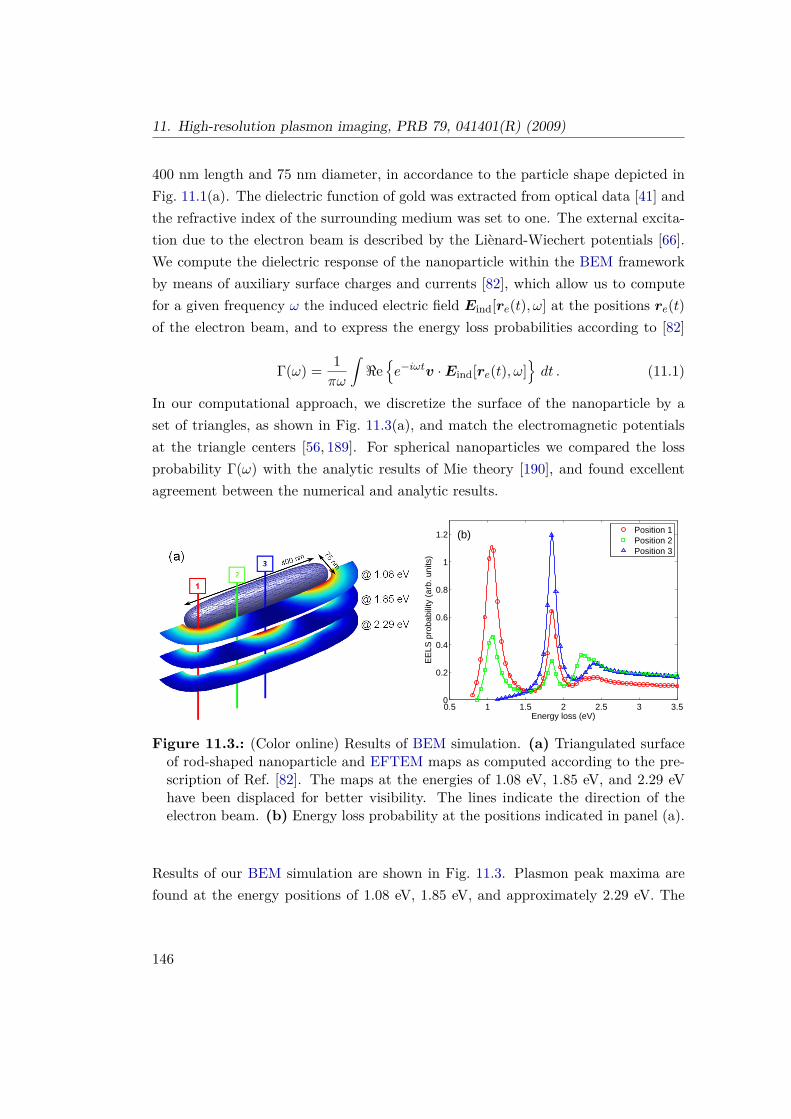
11. High-resolution plasmon imaging, PRB 79, 041401(R) (2009)
400 nm length and 75 nm diameter, in accordance to the particle shape depicted inFig. 11.1(a). The dielectric function of gold was extracted from optical data [41] andthe refractive index of the surrounding medium was set to one. The external excita-tion due to the electron beam is described by the Liènard-Wiechert potentials [66].We compute the dielectric response of the nanoparticle within the BEM frameworkby means of auxiliary surface charges and currents [82], which allow us to computefor a given frequency ω the induced electric field Eind[re(t), ω] at the positions re(t)of the electron beam, and to express the energy loss probabilities according to [82]
Γ(ω) = 1πω
∫<ee−iωtv ·Eind[re(t), ω]
dt . (11.1)
In our computational approach, we discretize the surface of the nanoparticle by aset of triangles, as shown in Fig. 11.3(a), and match the electromagnetic potentialsat the triangle centers [56, 189]. For spherical nanoparticles we compared the lossprobability Γ(ω) with the analytic results of Mie theory [190], and found excellentagreement between the numerical and analytic results.
0.5 1 1.5 2 2.5 3 3.50
0.2
0.4
0.6
0.8
1
1.2
Energy loss (eV)
EE
LS p
roba
bilit
y (a
rb. u
nits
)
(b) Position 1Position 2Position 3
Figure 11.3.: (Color online) Results of BEM simulation. (a) Triangulated surfaceof rod-shaped nanoparticle and EFTEM maps as computed according to the pre-scription of Ref. [82]. The maps at the energies of 1.08 eV, 1.85 eV, and 2.29 eVhave been displaced for better visibility. The lines indicate the direction of theelectron beam. (b) Energy loss probability at the positions indicated in panel (a).
Results of our BEM simulation are shown in Fig. 11.3. Plasmon peak maxima arefound at the energy positions of 1.08 eV, 1.85 eV, and approximately 2.29 eV. The
146

11.4. Discussion
spatial intensity distribution of the plasmonic modes fits the experimental findingsvery well, giving evidence that the detected peaks in the EELS spectrum can be in-terpreted as the resonance modes of the plasmon oscillations of the gold nanoparticle.We attribute the differences between the energetic positions of the peak maxima intheory and experiment to our neglect of the holey carbon film in the simulations,which is expected to red-shift the peak maxima and to introduce an anisotropy inthe simulated EFTEM maps. As regarding the peak at 2.29 eV, we find that it isstrongly broadened. This is attributed to interband scatterings in gold, that takeplace above a threshold of approximately 2 eV. We also found that the EFTEM mapof the 2.29 eV peak is smeared out when we compute the loss probabilities not at asingle energy, but integrate over an energy window of 0.4 eV to simulate the effect ofthe limited energy resolution in the experiments.
11.4. Discussion
The energy resolutions of both EFTEM and EELS is governed by the width of theZLP. Surface plasmons of silver nanoparticles have been mapped by EELS in anenergy regime above 1.70 eV, using cold field emission guns together with a de-convolution procedure applied to the raw data [108], but surface plasmons of goldparticles, which lie closer to the ZLP, can only be observed with a monochromatedsystem [191]. A monochromated beam has a truly symmetric energy distribution andno pronounced ZLP tails towards the low-loss regime, giving profound advantagesover cold field emission guns in this energy range [192]. An analysis of the full widthat half maximum of the ZLP, extracted from the data in the vacuum area, reveals forour setup an EFTEM energy resolution of 0.43 eV, to be compared with the EELSresolution of 0.17 eV. This higher spectral resolution of EELS is also apparent fromFig. 11.2, although in both cases the different plasmonic eigenmodes, whose spectralwidths are usually of the same order of magnitude, can be easily discriminated.
The advantage of EFTEM lies in its high spatial resolution over large field-of-views.It is important to realize that any attempt to obtain mapped EELS images withcomparable spatial sampling is not simply more cumbersome or time-consuming, butis probably doomed to failure for the following reason. A difficulty for extreme low-
147

11. High-resolution plasmon imaging, PRB 79, 041401(R) (2009)
loss mapping is posed by the strong intensity difference between the ZLP and theadjacent low-loss region, which challenges the dynamic range of the detector. Thesituation is even worse for a monochromated source, as the ZLP maximum becomesstronger with decreasing peak width. While it is possible to choose a setup whichtruncates the most intense parts of the ZLP by shifting the spectrum just acrossthe edge of the detector, this technique relies on the stability of the system withrespect to energy offsets over the time of acquisition. Considering the pixel dwelltime of about 0.6 sec, which includes both the exposure time of 0.1 sec and thedata readout of the detector, a spatial map of 512 × 512 data points would havetaken close to 36 hours, during which energy drift must not have exceeded 0.5 eV.Such long time stability can hardly be achieved in any modern system. In contrastto the scanning beam approach, within EFTEM the energy dimension is sampledsequentially and the dynamic range problem close to the ZLP can be overcome byespecially adapted acquisition routines [188]. A second advantage of EFTEM isits ability to rapidly image large areas at lower magnification, without tediouslyadjusting the electron beam to coarse sampling conditions. For instance, imagingthe spatial distribution of the 1 eV peak alone would have required only 1 minute,thus demonstrating the unique capability of mapping large field-of-views with spatialresolution on the nanometer scale. Furthermore, in a scanned beam approach spatialdrift during acquisition can lead to map distortions, which can not be corrected oreven unambiguously identified from the data alone, whereas spatial consistence ofEFTEM images is immediately evident.
In conclusion, we have shown that EFTEM imaging can be used to directly andefficiently visualize the electromagnetic eigenmodes of surface plasmons in metallicnanoparticles. The technique surpasses the spatial resolution of optical measure-ments by more than one order of magnitude and still allows for large field-of-viewsto be investigated within several minutes. Therefore, detailed studies of assembledparticles or structured devices become available, bridging the gap between highly re-solved local measurements, such as STEM EELS, and optical microscopy techniques,which average over larger areas and smear out inhomogeneities on a nanometer scale.The technique can also be applied for fast screening of many particles with slightlydifferent resonance frequencies, or to localize “hot spots” of strongest resonance ina device, prior to detailed local analysis. It could also be advantageous for beam
148

11.4. Discussion
sensitive samples, where high dose rates of a focused beam may alter the structurelocally during the measurement, whereas rapid parallel illumination of the sample al-lows for snap shots of an undamaged specimen. It should be emphasized that a beammonochromator is paramount for resolving plasmon energies around and below 1 eV,which constitutes an important energy range for Au nanoparticles. We believe thatEFTEM will not supersede the scanning EELS approach as a high-spatial-resolutionand high-energy-resolution technique in general, but will amend its capabilities withrespect to the spatial domain.
We thank Harald Ditlbacher and Franz Aussenegg for most helpful discussions. Thiswork has been supported in part by the FWF under project P18136–N13, and by theZukunftsfonds Steiermark.
149


12. PAPER: Influence of surfaceroughness on the optical properties ofplasmonic nanoparticles
Andreas Trügler, Jean-Claude Tinguely, Joachim Krenn, Andreas Hohenau,and Ulrich Hohenester
Institut für Physik, Karl–Franzens–Universität Graz,Universitätsplatz 5, 8010 Graz, Austria
Published in: Phys. Rev. B 83, 081412(R) (2011)
Abstract
For plasmonic nanoparticles, we investigate the influence of surface roughness in-herent to top-down fabrication on the optical properties, and find that it has asurprisingly small influence on the position and width of the plasmon peaks. Ourexperimental observation is supported by simulations based on the boundary elementmethod approach. Using a perturbation approach, suitable for metallic nanoparti-cles with a moderate degree of surface roughness, we demonstrate that the reason forthis lies in motional narrowing where the plasmon averages over the random heightfluctuations. Surface roughness in large arrays of identical nanoparticles, such asencountered in the context of metamaterials, is thus expected to not constitute amajor roadblock.
151
12. Influence of surface roughness, PRB 83, 081412(R) (2011)
12.1. Introduction
Plasmonics bridges the gap between the micrometer length scale of light and thelength scale of nanostructures [45]. This is achieved by binding light to coherentcharge density oscillations of metallic nanostructures, so-called surface plasmons,which allow to focus electromagnetic radiation down to spots with spatial dimen-sions of the order of a few nanometers [193]. Coupling of quantum emitters, suchas quantum dots or molecules, with plasmonic nanostructures can strongly modifytheir excitation and emission properties, observable in fluorescence [180] or surfaceenhanced Raman scattering, [194] and offers a unique means for tailoring light-matterinteraction at the nanoscale. This has found widespread applications ranging from(bio)sensors [7] and solar cells [20] to optical and quantum communication technol-ogy [195]. Plasmonic nanoparticles are also at the heart of the emerging fields ofmetamaterials and optical cloaking [196].
Huge advances in fabrication techniques over the last years allow nowadays to fab-ricate plasmonic nanostructures with well understood and predictable properties.Nevertheless, practically all metallic nanoparticles suffer from size inhomogeneitiesand nanoscale surface roughness, [197, 198] which results in deviations of the plas-monic properties from those of idealized nanoparticles [199]. Particularly top-downapproaches for nanoparticle fabrication often involve vacuum deposition of the metalstructures, which leads to polycrystalline particles with an apparent surface rough-ness [198]. Despite the important role of surface roughness, there is still little un-derstanding about the impact of such imperfection on the optical properties. Recentpublications report on the control of nanoscale roughness and its strong effect on thenanoparticles far- and near-field optical properties [197, 198, 200]. However, varyingsurface roughness is often accompanied by varying crystallinity, and therefore theresults do not allow for a clear distinction between the contributions of the surfaceand the bulk.
In this Letter we provide evidence from experiment, theory, and simulation thata moderate amount of surface roughness has no significant impact on the far-fieldoptical properties of metallic nanoparticles. We interpret this as a kind of motionalnarrowing, where the surface plasmon averages over the random height fluctuationsof the metal surface, which leads to destructive interference and an overall small net
152

12.2. Experiment
effect. Our findings might be beneficial for the design of metamaterials, which relyon large ensembles of practically identical particles, as well as devices based on thefar-field properties of plasmonic nanoparticles.
12.2. Experiment
Wemeasured the scattering spectra of individual polycrystalline (rough) gold nanopar-ticles to probe the influence of unavoidable surface roughness on the plasmonic sig-nature of nanoparticles of nominally identical shape. The particles were fabricatedby electron beam lithography on an ITO covered glass substrate. The substratewas coated with a polymer resist, which was then exposed and chemically developed.Vacuum deposition of gold and a liftoff process lead to polycrystalline particles (crys-tallite size ∼ 20 nm) of designed shapes, [201] but with apparent surface roughness,as shown in Fig. 12.1(b). The particles were probed in a dark field microscope, col-lecting the scattered light by a 40×, 0.75 numerical aperture objective and analyzingit with a spectrograph.
Fig. 12.1(a) shows exemplarily scattering spectra of four individual 50 nm wide,100nm long, and 45nm high gold nanorods. Although the exact particle shapes differdue to nanoscale roughness [Fig. 12.1(b)], the dipolar plasmon resonance positionsand the spectral widths of the four particles under consideration differ less then 20%of the full width at half maximum. Similar results were also observed for othernanoparticle shapes (not shown). From this we conclude that surface roughness hasa surprisingly small influence on the optical properties of plasmonic nanoparticles,at least in the regime where the roughness does not lead to a noticeable change ofthe particle aspect ratio.
12.3. Simulation
We additionally performed simulations based on the Boundary Element Method(BEM), [23, 56, 82, 83] using a dielectric function representative for gold [41] anda refractive index of nb = 1.65 for the substrate. The particle shapes in the (x, y)-plane were extracted from the SEM images [Fig. 12.1(c)]. We use a particle height of
153

12. Influence of surface roughness, PRB 83, 081412(R) (2011)
Figure 12.1.: (color online) (a) Scattering spectra of four individual gold nanorodsexcited with a polarization parallel to the particles long axis. (b) Spectra simu-lated within a BEM approach, using the gold dielectric function of Ref. [41] anda refractive index of nb = 1.65 for the substrate, for the particle shapes extracedfrom the SEM images reported in panel (c). The particle height is 45 nm. Thelength of the scalebar in the lower panels is 100 nm.
154

12.3. Simulation
45 nm and round off the edges with a curvature radius of 5 nm. Scattering spectraare reported in Fig. 12.1(b). In accordance to experiment, we find a surprisinglysmall influence of the particle shape on the plasmon peak positions. Also the abso-lute peaks heights (not shown) vary by less than 5 percent. We note that there aresubtle differences between experiment and theory, such as the weak shoulder around2 eV, which might be indicative of another excited mode sustained by its particularthree-dimensional shape.
To inquire into the reasons for the observed behavior, in the following we use cylindri-cal nanorods as a showcase system, because of their extreme sensitivity to variationsof the dielectric environment and shape [156]. We also employ the quasistatic ap-proximation, [82, 85] which is justified for small particles and will allow us furtherbelow to introduce a perturbation analysis. With respect to the retarded BEM sim-ulations, the quasistatic approximation is expected to lead to a slight overestimationof the plasmon peak energy.
In our simulations, we model surface roughness by adding stochastic height variationsto the smooth surface of an ideal nanoparticle. In two dimensions and for a box withperiodic boundary conditions, height variations with a Gaussian autocorrelation canbe obtained by attaching to all Fourier coefficients arbitrary phase factors eiφrnd viz.
h(x, y) = ∆h<e[F−1
(e−
12 ς
2h(k2
x+k2y)+iφrnd
)− 1
2
], (12.1)
where F−1 denotes the inverse Fourier transform and ς2h is the variance of the height
fluctuations. We next map h(x, y) to the nanoparticle surface and displace the ver-tices of the nanoparticle along the surface normal directions1. A typical realizationof surface roughness is depicted in Fig. 12.2(b) for a nanorod.
Figure 12.2(a) shows spectra for gold nanorods for different height-to-diameter ratios.Throughout we set the rod diameter to 30 nm and use ςh = 3 nm. For each spectrum
1Mapping can be faciliated by computing h(x, y, z) in three dimensions, with an expression similarto Eq. (12.1), and interpolating the stochastic height variations h to the nanoparticle surface.
155

12. Influence of surface roughness, PRB 83, 081412(R) (2011)
1 1.2 1.4 1.6 1.8 2 2.20
0.2
0.4
0.6
0.8
1
1.2
1.4
1.6
1.8
2
↓Rippled rod
2.0 nm
3.5 nm
5.0 nm
Δ h 2 : 13 : 14 : 1 (a)
x 15x 2
Photon energy (eV)
Sca
tterin
g cr
oss
sect
ion
(arb
. uni
ts)
Figure 12.2.: (color online) (a) Simulated spectra for nanorods with a diameter of30 nm and for height-to-diameter ratios of 2 : 1, 3 : 1, and 4 : 1. In our simulationswe use a dielectric function representative for gold [41] and a homogeneous dielec-tric background (nb = 1.5), and add stochastically surface roughness according tothe prescription of Eq. (12.1) with ςh = 3 nm and for different ∆h values, whichdetermine the height variations of surface roughness. Each spectrum is averagedover 100 randomly generated nanoparticles. The gray lines report results for rip-pled rods, as discussed in the text. The spectra for ratios 2 : 1 and 3 : 1 have beenmagnified by factors of 15 and 2, respectively. (b) Surface charge distributions σafor the optically active plasmon modes for the smooth (left), rippled (middle), andrough (right) nanorods.
156

12.4. Theory
we average over hundred random realizations of surface roughness and assume lightexcitation with a polarization along long axis of the rod. One clearly observes thatwhen increasing the amount of surface roughness, by choosing different values of ∆h,the shape of the averaged spectra does not change (with exception of an overall smallred shift). Only the variance of the individual spectra increases with increasing ∆h,as indicated by the errorbars. Thus, our numerical simulations again demonstratethat surface roughness has a surprisingly small influence on the optical properties ofplasmonic nanoparticles.
Things change considerably if we use the more regular height variations of a rippledrod, depicted in Fig. 12.2, that was recently suggested as a viable model for surfaceroughness [202]. Here the spectra strongly shift to the red when ∆h is increased, asdepicted by the gray lines on the left of Fig. 12.2. Thus, it appears that the irregularshape of the surface height fluctuations is responsible for the overall small shift ofthe plasmon peak position. Indeed, when ripples are introduced not only along thesymmetry axis of the nanorod but also around its circumference (here 6 ripples) theredshift becomes strongly reduced, as shown by the dashed gray lines.
12.4. Theory
We next develop a perturbation analyis which will help us to understand the effectsof surface roughness more deeply. Let us first recall the basic elements of the BEMapproach. For a metallic nanoparticle with dielectric function εm(ω) embedded in adielectric background with constant εb, the solutions of the Poisson equation withinthe two media are given by the Green function G(r,r′) = 1/|r−r′|. The electrostaticpotential can be written in the ad-hoc form Φ =
⟨G, σ
⟩+φext [82], where σ is a
surface charge distribution located at the boundary ∂Ω of the metallic nanoparticle,which has to be chosen such that the boundary conditions of Maxwell’s equationsare fulfilled, 〈G, σ〉 =
∫∂Ω G(r,s)σ(s) ds defines an inner product, and φext is the
potential of the external perturbation.
Continuity of the normal component of the dielectric displacement at the metal-dielectric interface gives an expression
157

12. Influence of surface roughness, PRB 83, 081412(R) (2011)
Λ(ω)σ +⟨∂G
∂n, σ
⟩= −∂φext
∂n, Λ = 2πεm + εb
εm − εb(12.2)
that can be used for the calculation of the surface charge distribution. Here ∂G/∂n ≡F and ∂φext/∂n ≡ φ′ext denote the surface derivatives of the Green function and theexternal potential, respectively.
We next define the right and left eigenvectors σRk and σLk of the surface derivative ofthe Green function through [85,86]
⟨F, σRk
⟩= λk σ
Rk ,
⟨σLk , F
⟩= λk σ
Lk , (12.3)
which form a biorthogonal set with⟨σLk , σ
Rk′
⟩= δkk′ . The functions σRk can be
interpreted as the surface plasmon eigenmodes, and the response to any externalperturbation can be decomposed into these modes viz.
σ = −∑k
σRkΛ(ω) + λk
⟨σLk , φ
′ext⟩. (12.4)
Apparently, a given mode k gives a noticeable contribution only if the coupling⟨σLk , φ
′ext
⟩to the external potential (in our case plane wave illumination) is suffi-
ciently strong and if the denominator becomes small. The plasmon resonance con-dition translates to <e [Λ(ω) + λk] = 0. This is an extremely useful expression asit allows to separate the structural properties (described by λk) from the materialproperties (described by Λ).
We are now in the position to analyze the effects of a moderate surface roughness,which we model as a distortion of the surface ∂Ω from its ideal shape. In turn, thesurface derivative of the Green function F changes to F+δF , where δF is expectedto have the same random character as the surface fluctuations2. How does λk, which
2This is because F (s,s′) is governed for s ≈ s′, where deviations of the ideal shape are mostsignificant, directly by the surface curvature.
158

12.4. Theory
determines the peak positions of the plasmons, change in case of surface roughness?When δF is sufficiently small we can employ perturbation theory, in complete anal-ogy to quantum mechanics. We treat F as the unperturbed part and δF as the“perturbation”. Following Ref. [87] we introduce for a given plasmon mode a theprojector
Q0a≡∑k 6=a
σR,0k σL,0k
λ0a − λ0
k
, (12.5)
where the superscript 0 indicates the eigenvalues and eigenfunctions for the idealnanoparticle surface. The corrections to λa then become within lowest order pertur-bation theory
λ1a =
⟨σL,0a , δFσR,0a
⟩(12.6a)
λ2a =
⟨σL,0a , δF
Q0aδF σR,0a
⟩. (12.6b)
From this we can draw an important conclusion for the dipolar modes, whose σR,0a
distribution usually varies smoothly on the length scale of surface roughness. SinceEq. (12.6a) averages the random variations δF over the unperturbed distributionsσR,0a , the positive and negative δF values associated with the height variations ofsurface roughness will become effectively averaged out. This results in a small λ1
a
correction, and consequently surface roughness does not affect significantly the opti-cally active plasmon modes.In a sense, this finding is similar to motional narrowing in semiconductor quantumwells [113], where the motion of an optically excited electron-hole pair (exciton) issubject to the potential induced by the local monolayer fluctuation inherent to quan-tum wells. When the exciton propagates through the well it “averages” over thefluctuations of the random potential, which results in a narrowing of the excitonlineshape.
In Fig. 12.3 we compare the results of our full simulations with the predictions ofEq. (12.6). The open and full symbols show the true resonance energies (obtainedfrom <e [Λ(ω) + λk] = 0) and the perturbation results (obtained with λ0
a + λ1a and
159

12. Influence of surface roughness, PRB 83, 081412(R) (2011)
1.2 1.4 1.6 1.8 21.1
1.2
1.3
1.4
1.5
1.6
1.7
1.8
1.9
2
2.1
Rippled rod (4 : 1)
2 : 1
3 : 1
4 : 1
O(1)
O(2)
Δ h = 2 nm 3.5 nm 5 nm
Resonance energy (eV)
Res
onan
ce e
nerg
y fr
om p
ertu
rbat
ion
theo
ry (
eV)
1.35 1.4 1.451.35
1.4
1.45
1.5
Figure 12.3.: (color online) Comparison of full simulations and perturbation theoryof Eq. (12.6), for the positions of the resonance energies of the optically activesurface plasmon modes with polarization along the long axis of the rod. The openand filled symbols report results obtained within first and second order perturba-tion theory, respectively. In the inset we show a blow-up for the nanorod with aheight-to-diameter ratio of 4 : 1.
λ0a + λ1
a + λ2a, respectively). Symbols on the diagonal correspond to the situation
where perturbation theory and the full BEM simulations coincide. In all cases theshift of the resonance with respect to the positions of the smooth nanorod (dashedhorizontal lines) is small. Quite generally, first order perturbation theory, whichignores any variations of the surface charge distribution (σa = σ0
a), leads to a blueshift. Only for second order perturbation theory, which includes modification of σa,the red shift of the plasmonic resonances is properly reproduced.
12.5. Summary
In summary, we have investigated the influence of surface roughness on the opticalproperties of plasmonic nanoparticles, and have found a surprisingly small effect.Using a simulation and perturbation theory approach, we have been able to traceback our findings to a motional narrowing, where the plasmon averages over therandom height fluctuations. As no corresponding conclusions prevail for the near-field optical properties, our results do not invalidate the findings of “hot spots” in
160

12.5. Summary
fluorescence or surface enhanced Raman scattering experiments. This work has beensupported in part by the FWF under project No. P21235–N20.
161


13. PAPER: Tailoring spatiotemporallight confinement in single plasmonicnanoantennas
Tobias Hanke1, Julijan Cesar1, Vanessa Knittel1, Andreas Trügler2,Ulrich Hohenester2, Alfred Leitenstorfer1, and Rudolf Bratschitsch1
1 Dep. of Physics and Center for Applied Photonics, Univ. of Konstanz, Univ.str. 10, D–78457 Konstanz2 Institut für Physik, Karl–Franzens–Universität Graz,Universitätsplatz 5, 8010 Graz, Austria
Published in: Nano Lett. 12, 992 (2012)
Abstract
Plasmonic nanoantennas are efficient devices to concentrate light in spatial regionsmuch smaller than the wavelength. Only recently, their ability to manipulate pho-tons also on a femtosecond timescale has been harnessed. Nevertheless, designingthe dynamical properties of optical antennas has been difficult since the relevant mi-croscopic processes governing their ultrafast response have remained unclear. Here,we exploit frequency resolved optical gating to directly investigate plasmon responsetimes of different antenna geometries resonant in the near infrared. Third-harmonicimaging is used in parallel to spatially monitor the plasmonic mode patterns. Wefind that the few-femtosecond dynamics of these nanodevices is dominated by ra-diative damping. A high efficiency for nonlinear frequency conversion is directlylinked to long plasmon dephasing times. This single parameter explains the counter-intuitive result that rod-type nanoantennas with minimum active volume generate byfar the strongest third-harmonic emission as compared to the more bulky geometriesof bowtie-, elliptical- or disc-shaped specimens.
163

13. Light confinement in nanoantennas, submitted (2011)
13.1. Light confinement in nanoantennas
Metal nanoantennas hold great promise for applications in physics, chemistry andbiology since they convert propagating light to highly localized and strongly en-hanced electric fields [178,203,204]. Besides their favorable linear optical properties,nanoantennas have recently been shown to represent excellent nonlinear emitters oflight [78,205–207]. In order to understand the mechanisms that govern nonlinear lightemission on ultrafast timescales, steady-state characterization techniques such as two-photon photoluminescence [61, 171, 208–210], cathodoluminescence [211], dark fieldscattering spectroscopy [135, 212], scanning near field optical microscopy [213–215]and electron energy loss spectroscopy [108, 172] are insufficient. An extraordinarytemporal resolution is required in addition to a high spatial selectivity since plas-monic effects in metal nanoantennas occur on a few-femtosecond timescale. Onlyrecently, few-femtosecond fiber lasers became available generating pulse trains withunprecedented stability [216] and reaching the single-cycle limit [217]. Ultraprecisionstudies with parallel resolution both at the nanometer and femtosecond scales areenabled with these systems.
Here, we use third-harmonic spectroscopy to compare commonly used nanoantennashapes with respect to their nonlinear emission of light. Surprisingly, the highest in-tensity is not linked to a specific shape, but to the smallest antenna volume. Nonlinearimaging with sub-wavelength resolution reveals that the fundamental dipole modeof the plasmon is excited in all antenna types. We find that resonant nanoantennasin the near-infrared are radiation-damped systems. The few-femtosecond plasmondamping time is the only parameter that governs the intensity of coherent nonlinearlight emission of these single-mode nanodevices.
Tailor-made arrays of gold nanoantennas are fabricated by electron beam lithographyon fused silica substrates of 200 µm thickness. They consist of two arms separatedby a feedgap. Their dimensions have been carefully chosen to be exactly resonantto femtosecond excitation with linear polarization parallel to the long axis. (Supple-mentary Information, Tab. 13.1 and Fig. 13.6). Few-cycle laser pulses in the nearinfrared are generated by a mode-locked Erbium-doped fiber laser system working ata repetition rate of 40 MHz. The average power is typically adjusted to be 5 mW.Ultimate temporal resolution is achieved by an excitation bandwidth of 470 meV (450
164

13.1. Light confinement in nanoantennas
nm) and using a Cassegrain reflector (NA = 0.65) for focusing. The nonlinear emis-sion from single nanoantennas is collected in transmission geometry with a secondobjective (NA = 0.95), short-pass filtered (Schott BG39), dispersed with a gratingmonochromator (Acton Spectra Pro 2300i) and detected with a Peltier-cooled CCDcamera (Andor Newton DU 920P-BU).
Figure 13.1.: Nonlinear emission and plasmon damping from metal nanoantennasof different shapes. a, Measured (black dots) and calculated (black line) third-harmonic intensity depending on the plasmon damping time on a logarithmic scale.b – d, Measured and e – g, simulated interferometric autocorrelation traces of threeresonant nanoantennas, each with the autocorrelation trace of the instantaneousresponse from the substrate (black dashed line) shown for comparison. The rodantenna (d, g) exhibits a plasmon damping time of τ = 5.5 fs, the elliptical one(c, f) shows τ = 3.5 fs, and τ = 2.0 fs for the disc-shaped antenna (b, e). Antennadimensions are listed in Supporting Information, Tab. 13.1.
The most striking finding is the large intensity difference of the generated third-harmonic emission for different antenna shapes (Fig. 13.1 a). Even though all anten-nas are resonant for excitation with light polarized along the long axis, the rod an-tenna generates one order of magnitude more third-harmonic intensity than the ellip-tical structure. Compared to the disc-shaped antenna, an increase of even two ordersof magnitude is achieved. As we will show, the dynamical properties of the nanoan-tennas on the femtosecond timescale are key for understanding this phenomenon.
We use frequency resolved optical gating at the third-harmonic (THG-FROG) tomeasure the plasmon damping time τ of single nanoantennas directly in the time
165

13. Light confinement in nanoantennas, submitted (2011)
domain [78]. For this purpose, we collinearly excite the structures with two identicaltransients derived from a Mach-Zehnder interferometer and record the emitted THGsignal as a function of time delay between the pulses. Fig. 13.1 b – d show measuredTHG autocorrelation traces for three different antenna shapes. The electric fieldamplitude and phase of the driving laser pulse are retrieved from the THG-FROGmeasurement of the instantaneous response from the substrate surface. We simulatethe autocorrelation traces (Fig. 13.1 e – g) by assuming harmonic oscillation of theresonant plasmon with a single exponential decay [218]. The damping time constantτ represents the only free fit parameter. It is determined by comparison of the fringeamplitudes of the measured and simulated autocorrelation data. As may be seen inFig. 13.1, the disc-shaped specimen exhibits the shortest plasmon dissipation time ofτ = 2 fs. Note that this interval corresponds to only half a cycle of light at the fun-damental resonance frequency of 250 THz. The elliptical design follows with τ = 3.5fs. At τ = 5.5 fs, the rod antenna shows the longest storage time for the radiationenergy. Weak plasmon damping is associated with an effective build-up of the plas-mon oscillation, if driven on resonance. Therefore, a strong third-harmonic emissionresults despite the small active volume of these devices. Indeed, the measured decaytimes may be used to calculate the relative third-harmonic intensity within the har-monic oscillator model. The excellent agreement between theory and experiment inFig. 13.1 a clearly demonstrates that knowledge of the plasmon damping time alonesuffices to predict the nonlinear emission intensity from different nanoantennas.
We now turn to the question what determines the plasmon damping time and howit can be engineered. One important issue in this context is whether the shape ofthe nanoantenna plays a significant role or not. It is conceivable that the excita-tion of differing or even multiple antenna resonances governs the observed changesin the plasmon damping time. Therefore, we analyze the plasmonic mode patternsof different nanoantenna types. Fig. 13.2 a – e show scanning electron micrographs(SEM) of rod-, elliptical-, disc-, bowtie-, and cross-shaped antennas. Ultimate spatialresolution is achieved for nonlinear emission mapping by replacing the Cassegrainian(NA = 0.65) by an oil immersion objective (NA = 1.3). The ultrabroadband spec-trum of the pump laser is restricted to a bandwidth of 0.17 eV (225 nm) centered at0.97 eV (1.28 µm). We still achieve a pulse duration as short as 24 fs in the focusof the oil immersion objective (Supplementary Information, Fig. 13.7). The sample
166

13.1. Light confinement in nanoantennas
Figure 13.2.: Spatially resolved third-harmonic emission from five gold nanoan-tennas of different shape. a – e, Scanning electron microscope images. f – p,Measurement. The metal nanostructures are scanned through the focus of an oilimmersion objective (NA = 1.3) and excited by femtosecond laser pulses in thenear infrared. Third-harmonic emission intensity is depicted in a normalized colorscale as a function of position, recorded for horizontal f – k and vertical l – p linearpolarization of the excitation. q – u, Polar plots of the third root of the measuredthird-harmonic intensity as a function of the polarization angle of the excitingbeam. i – x, Boundary element simulations of the third-harmonic intensity forantenna geometries as in the experiment with horizontal i – v and vertical vi – xpolarization of the excitation. All scale bars are 300 nm.
167

13. Light confinement in nanoantennas, submitted (2011)
is raster-scanned within the confocal region with a step size of 50 nm and a dwelltime of 50 ms. Fig. 13.2 g – q depict spatial maps of third-harmonic emission fromsingle gold nanoantennas of different shapes. The free-space spatial resolution of ourexperiment is better than the lateral extension of the sub-wavelength antenna struc-tures (Supplementary Information, Fig. 13.7). This performance is achieved using athird-order nonlinear process resulting in a much shorter wavelength for imaging ascompared to the fundamental in the near infrared. It represents a distinct advantageover linear or lower-order optical methods [171,210] previously used to detect highermode patterns of single nanoantennas. Here, we directly resolve the fundamentalplasmonic mode which is accompanied by the highest field enhancement ( [61] andSupplementary Information, Fig. 13.8). We note that this technique is also idealfor rapid systematic investigations of nanoantennas. A typical high-resolution THGmap with 600 pixels and a signal to noise ratio better than 103 is recorded within 30seconds. For linear polarization of the excitation set parallel to the resonant antennaaxis (“horizontal”) the third-harmonic emission maps for all types of nanoantennas(Fig. 13.2 f – k) are found to exhibit the fundamental plasmon mode with a singlehotspot in the gap region. For excitation polarized perpendicular to the main antennaaxis (“vertical”) neither the rod nor the elliptical nanoantenna fulfill the resonancecondition for a near-infrared plasmon. As a consequence, the residual third-harmonicemission is at least three orders of magnitude weaker (Fig. 13.2 l, m) compared to thehorizontal configuration. The other three antenna shapes support plasmonic modesalso in the vertical direction (Fig. 13.2 n – p). The third-harmonic scans for thedisc- and bowtie- shaped antennas are similar. A two-lobed pattern occurs due tothe collective electron motion at the triangle bases and at the outer edges of thediscs as a result of restoring Coulomb forces. The cross antenna features again onehotspot in the center. We note that arbitrary polarizations may be converted to thenear field by this antenna type provided the gap size of the antenna is sufficientlysmall [219]. The dipolar behavior of the plasmonic modes is clearly seen in the polarplots (Fig. 13.2 q – u) of the maximum signal as a function of the direction of incidentlinear polarization.
In order to quantitatively analyze these mode patterns we have carried out simu-lations of third-harmonic emission from single nanoantennas by using a boundaryelement method (BEM) [82, 83]. The surface of the nanoantenna is discretized into
168

13.1. Light confinement in nanoantennas
triangles and the centroid of each triangle is taken as a collocation point where theelectromagnetic fields are matched (see Supplementary Information, Fig. 13.5). Weuse the dielectric function of gold extracted from optical data [41] and a refractiveindex of 1.35 (weighted average of substrate and air) for the embedding medium.The spatial dimensions of the metal nanostructures are analogous to the experiment(Supplementary Information, Tab. 13.1 and Fig. 13.6). We consider a Gaussian ex-citation spot (FWHM = 300 nm) and take the third power of the electric field atthe surface as source of the third-order polarizations. The coherent sum over thesenonlinear dipoles then results in the third-harmonic signal. In the lower panel ofFig. 13.2 i – x, we show the calculated THG maps. The theoretical results are almostperfectly in agreement with the corresponding experimental data above. Both, fromexperimental data and theoretical calculations of the spatial plasmonic patterns, wefind that the fundamental mode is exclusively excited in all antenna types. Hence,a mechanism independent of the shape must be the reason for the different plasmondamping times and the pronounced changes in the emitted THG intensities.
To resolve this question, the basic antenna geometry is kept constant and only oneantenna dimension is varied. Rod antennas with identical arm length (l = 260nm), gap distance (g = 50 nm) and thickness (h = 30 nm) but varying rod widthsare fabricated using electron beam lithography. Fig. 13.3 a shows the third-harmonicemission map of ten individual rod antennas. The nanodevices are spatially separatedby 3 µm from each other. The width of the antenna arms is increasing from w = 35nm on the left image side to w = 200 nm on the right. The inset of Fig. 13.3depicts the narrowest and the widest antenna under investigation. The extractedmaximum third-harmonic intensity as a function of rod width is plotted in Fig. 13.3b. It is apparent that the THG intensity follows an inverse cubic dependence withthe rod width identified by the straight line in the logarithmic plot of Fig. 13.3b. The experimental observation highlights that high nonlinear light emission isdirectly connected to small antenna volumes. This observation strongly hints toradiative damping in these metal nanostructures, which is proportional to the numberof coherently oscillating dipoles and therefore depending on the volume [220,221].
To prove this assumption we move back to the time domain and measure the plasmondamping times as a function of rod width of a second set of nanoantennas (s = 150nm, h = 20 nm, g = 50 nm). Although the variation in rod width causes a slight
169
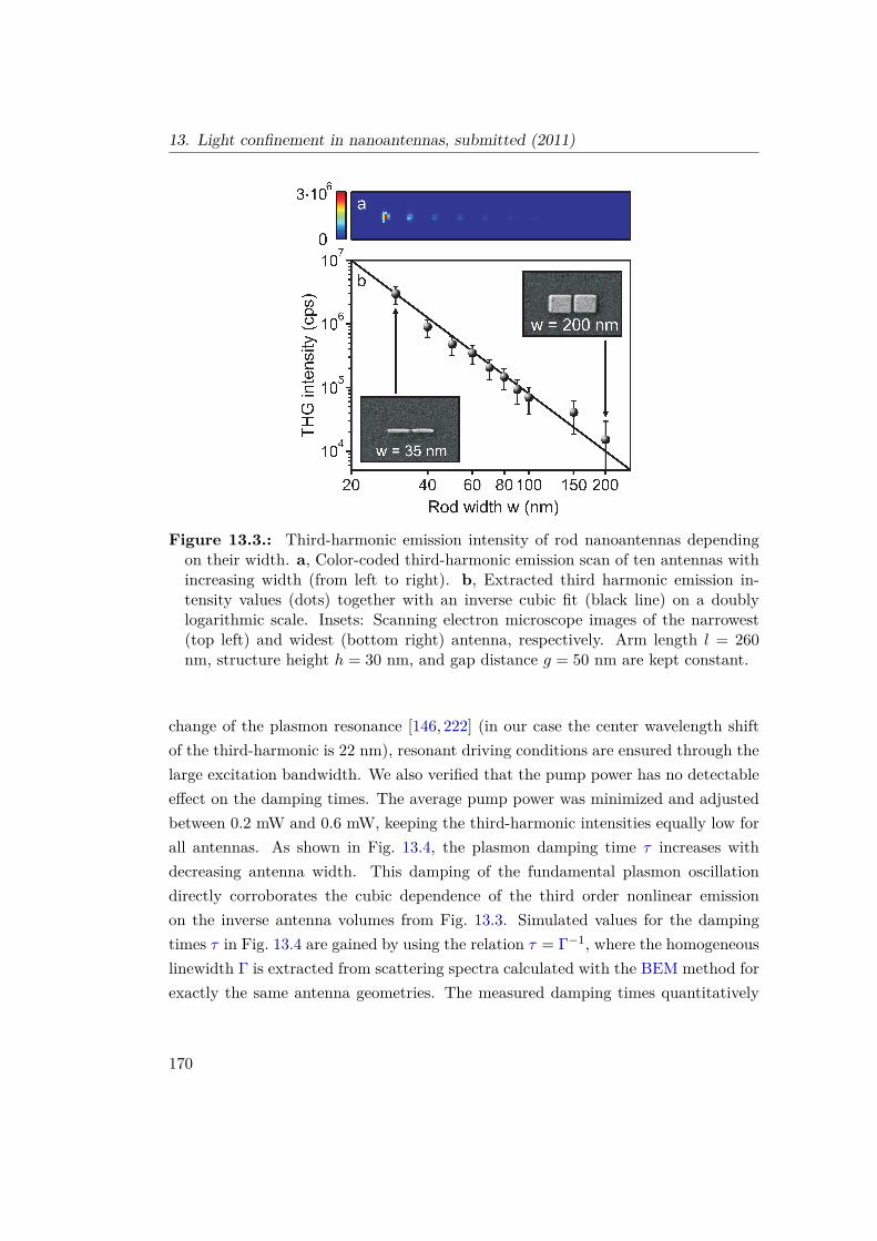
13. Light confinement in nanoantennas, submitted (2011)
Figure 13.3.: Third-harmonic emission intensity of rod nanoantennas dependingon their width. a, Color-coded third-harmonic emission scan of ten antennas withincreasing width (from left to right). b, Extracted third harmonic emission in-tensity values (dots) together with an inverse cubic fit (black line) on a doublylogarithmic scale. Insets: Scanning electron microscope images of the narrowest(top left) and widest (bottom right) antenna, respectively. Arm length l = 260nm, structure height h = 30 nm, and gap distance g = 50 nm are kept constant.
change of the plasmon resonance [146, 222] (in our case the center wavelength shiftof the third-harmonic is 22 nm), resonant driving conditions are ensured through thelarge excitation bandwidth. We also verified that the pump power has no detectableeffect on the damping times. The average pump power was minimized and adjustedbetween 0.2 mW and 0.6 mW, keeping the third-harmonic intensities equally low forall antennas. As shown in Fig. 13.4, the plasmon damping time τ increases withdecreasing antenna width. This damping of the fundamental plasmon oscillationdirectly corroborates the cubic dependence of the third order nonlinear emissionon the inverse antenna volumes from Fig. 13.3. Simulated values for the dampingtimes τ in Fig. 13.4 are gained by using the relation τ = Γ−1, where the homogeneouslinewidth Γ is extracted from scattering spectra calculated with the BEM method forexactly the same antenna geometries. The measured damping times quantitatively
170

13.1. Light confinement in nanoantennas
Figure 13.4.: Plasmon damping time of rod nanoantennas of different widths.Measured values are depicted as dots, while the simulated values are drawn as asolid line. Nanoantenna dimensions are: arm length l = 150 nm, height h = 20nm, and gap distance g = 50 nm.
agree with simulated ones, which finally proves that our infrared nanoantennas withvolumes between 1.4×10⁻²² m3 and 3.4×10⁻²¹ m3 are indeed dominated by radiativedamping. Given that this is a purely dissipative process, we always discuss the energyrelaxation time τ . Under our conditions, τ is directly linked to the decoherence timeT2 of the oscillation amplitude via T2 = 2τ [223, 224]. We would like to note thatfor gold nanorods with volumes below 0.6 × 10⁻²² m3 and resonant in the adjacentvisible range, damping was attributed to electronic interband transitions [135]. Onlyfor small probed volumes and at higher plasmon energies, loss mechanisms such ascarrier-carrier, carrier-lattice, and surface scattering become increasingly important[225, 226]. In the near infrared, however, metal antennas are limited solely by theprocess they are intended for, namely radiation coupling.
In conclusion, we have presented nonlinear emission spectroscopy as a new power-ful tool to characterize and design single metal nanoantennas in space and time.On the temporal scale, few-femtosecond plasmon damping times are directly mea-sured for different antenna shapes. Due to radiative damping the lowest active vol-umes generate by far the strongest third-harmonic emission. On the spatial scale,
171

13. Light confinement in nanoantennas, submitted (2011)
the third-harmonic emission of different types of nanoantennas is mapped out toprove operation at the fundamental mode. By combining sub-wavelength concentra-tion in space with few-cycle response times, the ultimate manipulation of light hasbeen demonstrated in all four dimensions. Our findings provide design capabilitiesfor nanoantennas with either an ultrabroadband spectral coverage or low radiativedamping rates accompanied by maximum nonlinear efficiencies. This knowledge willalso be decisive for the creation of tailored hybrid antenna-nanoemitter systems forapplications in few-photon quantum optics on a femtosecond timescale [227].
172

13.2. Supplementary Information
13.2. Supplementary Information
Figure 13.5.: Details of the simulation via the boundary element method. Surfacediscretization (upper halves of each plot) and real part of the normalized surfacecharges (lower halves) of the five investigated nanoantennas under resonant exci-tation with horizontal polarization. Together with surface currents they are usedfor solving Maxwell’s equations [82, 83]. The number of surface elements variesbetween 10000 and 20000. The dielectric function for gold is extracted from opti-cal data [41] and a refractive index of 1.35 is adopted for the embedding medium(corresponding to a weighted average of fused silica substrate and air).
Antenna shape Rod Ellipse Disc Rod Ellipse Disc Bowtie CrossFigure 13.1d 13.1c 13.1b 13.2a 13.2b 13.2c 13.2d 13.2e
Arm length l 240 260 250 305 280 300 295 280Arm width w 45 100 250 60 110 300 240 285Height h 35 35 35 35 35 35 40 35Gap distance g 50 45 45 65 50 45 60 90
Table 13.1.: Antenna dimensions in nm of Fig. 13.1 and 13.2 retrieved from scanningelectron micrographs with an uncertainty of 5 nm. Identical dimensions are usedfor the simulated nanostructures.
173

13. Light confinement in nanoantennas, submitted (2011)
300 600 900 1200 1500 18000
0.2
0.4
0.6
0.8
1
wavelength (nm)
scattere
d in
tensi
ty (
a. u.)
horizontal polarization
rod
ellipse
disk
bowtie
cross
600 900 1200 1500 1800
vertical polarization
a b
T. Hanke et. al., Figure S5.
300
Figure 13.6.: Simulated scattering spectra for the five nanoantennas of Fig. 13.2for horizontal a and vertical b linear polarization. While in the experiment thestructures are optimized to yield maximum third-harmonic emission when drivenin the wavelength range between 1.2 µm and 1.5 µm, the nominal nanoparticle di-mensions (see Tab. 13.1) are taken without further optimization in the simulation.As a result, the maxima of the emission peaks are varying. We account for thiseffect by setting the central frequency of the ultrabroadband femtosecond pulseresonant to the scattering maxima.
174

13.2. Supplementary Information
pump power (mW)
TH
G in
ten
sity
(ct
s/s)
1 2 30.0
0.5
1.0
photon energy (eV)
spe
ctra
l in
ten
sity
EXC
THG
anntena
subtr
tes
a
a
c
-100 0 1000
16
32
delay time (fs)
TH
G a
uto
corr
ela
tion
b t = p
24 fs
-1 0 10.0
0.5
1.01.0
relative position (µm)
TH
G in
ten
sity
d s =
356 nm
1 2 4 810
1
104
107
T. Hanke et. al., Figure S1.
Figure 13.7.: Experimental details for third-harmonic imaging with sub-wavelengthspatial resolution of Fig. 13.1 and 13.4. a, Excitation (red) and third-harmonic(blue) intensity spectrum. b, Measured (blue) and simulated (black) third-harmonic intensity autocorrelation, retrieving a pulse duration of 24 fs. c, Pump-power dependence of the third-harmonic intensity for the fused silica substrate(blue) and a resonant rod antenna (red) together with cubic fits on a logarithmicscale. Note that the intensities differ by five orders of magnitude. d, Horizontalcut (blue dots) through the measured third-harmonic emission map of Fig. 13.1 itogether with a Gaussian fit (blue line), yielding a FWHM of 504 nm.
175

13. Light confinement in nanoantennas, submitted (2011)
200 400 600 800 100010
-3
10-2
10-1
100
rod length l (nm)
TH
G in
tensi
ty (
a.u
.) a) Fund. int. (cts/s) 0 450
3 µm
x 6
x 6
a
b
Hanke et. al., Figure S2.
1 2 3 4 5 6 7 8 9 10 11 12 13 14 15 16
3
4
5
6
7 8
9
10
11
12
14 16
17 18 19 20 21 22 23 24 25 26 27 28 29 30 31 32
33 34 35 36 37 38 39 40 41 42 43 44 45 46 47 48
18
23
25 27
29 32
37
43 47
wl
Figure 13.8.: Third-harmonic intensity of single gold nanorods on a fused silicasubstrate as a function of their length. a, Third root of the third-harmonic intensityscan (color coded) of 48 neighboring rods with rod length increasing from left toright and top to bottom. Note the successive appearance of higher resonances.b, Projection of the THG intensity values (black dots) to the corresponding rodlengths on a logarithmic scale. Despite the drastic THG intensity decrease we canidentify up to the fourth mode. The inset shows a SEM image of one specimenwith length l = 1.7 µm. The width w = 50 nm and thickness t = 30 nm of thenanoantennas are kept constant.
176

Part III.
Résumé
177


14. Summary
14.1. What has been done
In this work we have discussed many aspects of the optical properties of metallicnanoparticles, ranging from the tunability of the plasmonic resonance to the ultrafastdynamics of the light-matter interaction. We have elaborated the theoretical descrip-tion of metallic nanoparticles in terms of classical field theory, where the microscopicmaterial response is lumped in the dielectric description. Besides the analytical solu-tion for spheres and ellipsoids we have introduced the BEM and the DDA as versatilesimulation tools for the numerical solution of the considered systems.
After the introductory chapters that should highlight the basics of plasmonic interac-tions and plasmon imaging, we presented a reprint of six papers, where we discussedthe properties of an optimal plasmon sensor, the possibility to map the plasmonicLDOS with EELS and Moiré imaging, the influence of surface roughness and theeffect of plasmon dephasing on the light confinement in single nanoantennas.
14.2. What is left to do
Our mnpbem toolbox covers a broad area of simulation possibilities, but there isstill plenty of room for improvements of course. For example a better interpolationscheme beyond the discussed collocation method as well as further code optimizationsshould be discussed. Another aspect that has not been addressed in this thesis is theinfluence of substrate effects, which, nevertheless, can be calculated with our toolbox.Besides the detailed testing of substrate effects we will also investigate grating effects,that come into play in the simulation of particle arrays and grids.
179

14. Summary
One of the limitations listed in Sec. 4.5.3 is the possibility of charged particles, whichoccur in electrochemistry, for example. This is something which in principle can alsobe included within our mnpbem toolbox, where the eigenmode expansion allows toincorporate an additional surface charge – but further investigation on this topic isalso necessary.
Another very interesting topic that will keep us busy in the next time, is the pos-sibility to generate holographic images of metallic nanoparticles with EELS [228].This represents a very nice continuation of our EELS simulations and will hopefullyallow deeper insights on the nonlocal interaction of high energetic electron beamswith particle plasmons.
The key to success in any kind of fundamental research is to find the unexpectedand forcing science into the corset of forecasted directions will not work. Thus theprediction of future perspectives in any kind of research field is inherently risky.Nevertheless because of the highly diverse nature of plasmonics we can assume anexciting future and high activity in this field as discussed in [229], where, for exam-ple, the merging of plasmonics with quantum systems, active plasmonic devices orbiochemical applications are named as future trends.
There are still many other open questions to explore and we are looking forward tonew challenges and tasks.
180

Acknowledgments
When I finished my studies and got to decide which path on the scientific road Ishould take, I got the wise and simple advice to just trust my gut feeling. Well,this is what I did and the person who gave me this advice turned out to be a reallygreat supervisor and a brilliant physicist. I want to thank Ulrich Hohenester forhis guidance, his patience, for conveying his passion for physics and his directness.In his subtle way he constantly encouraged me and not even once I found his doorclosed when I was looking for his help and advice. He has a great talent to bringclearness into intricate problems and I’m still sometimes impressed with how quicklyand efficiently he solves such difficulties.Furthermore, I sincerely thank Joachim Krenn, Alfred Leitner, Andreas Hohenau,Jean-Claude Tinguely, Daniel Koller and all other members of the Optical Nan-otechnology / Nano-Optics group in Graz for most helpful discussions. I guess thestraightforwardness and simplicity of our collaboration serves as a role model of fruit-ful teamwork which demonstrates how easily experimental and theoretical work canbe enriched from each other.
I also want to express my gratitude for all my other collaborations, namely:
• the research group of Carsten Sönnichsen at the Institute for Physical Chem-istry in Mainz, where Jan Becker and others did a marvelous job in putting ourMatlab® toolbox to the acid test,
• the group of Alfred Leitenstorfer from the Lehrstuhl für Moderne Optik undQuantenelektronik – especially Tobias Hanke and Rudolf Bratschitsch (whochanged to Chemnitz University of Technology in the meantime),
• the group of Ferdinand Hofer at the Austrian Centre for Electron Microscopyand Nanoanalysis (Felmi) in Graz,
181

14. Summary
• Birgit Wiedemann and Michael Kaniber from the Walter Schottky institute(Center for Nanotechnology, Munich University of Technology), and
• Christoph Huber from the group of Wolfgang Kautek at the Institut für Physikalis-che Chemie in Vienna.
Special thanks also go to the theoretical and computational nanoscience group of ElisaMolinari in Modena for a great research stay at the beginning of my PhD, where Iwas welcomed most cordially particularly by Rosa DiFelice and Guido Goldoni.
On a more personal basis, I would like to thank my family and friends. My parentssupported me in every possible way, and no matter what difficulties there may come,my family will always bolster me. Without my two siblings, Thomas and Christine,life would be so much less fun and it is remarkable how different and how similar weare at the same time. It is really calming to know that there will always be a tablelarge enough in my parents’ house, where we all can come together.Speaking of a heartily atmosphere, also every visit with Rosmarie and Thomas inSaalfelden leads to a replenishing of my batteries and when I see the rocky face ofthe Steinernes Meer it warms my heart – the difficulty of the plains are forgotten.
But above all I owe my deepest thankfulness to Steffi, for her love, her encouragementand for letting me see the real important things when sometimes the blinders ofphysics obscure my view.
I also want to thank Wolfgang, Markus, Daniela and Birgit, Gernot and Sabine, Gabi,Julia, Markus and Birgit, and all the others, who may forgive me for this incompletelist, for their heartfelt and deep friendship, and for accompanying me in my life. Ialso want to express my deep gratitude to Michi for our unforgettable trips to frozenwaterfalls and glaciated mountain tops – feeding upon these memories keeps my headabove water when every now and then the daily routine prevails. Special thanks alsogo to Jürgen (and his unshakable humor), who helped me to identify errors and typosin this work.Last but not least I owe thanks to Richard Forsyth for many useful comments con-cerning the spelling in this thesis. In this respect, also the helpful remarks and adviceof Margot Grösslich were of great help to me – thank you for that!
182

Part IV.
Supplement
183


A. Appendix – Utilities
A.1. Boundary conditions at different media
By following [66], let V be a finite space volume bordered by the surface area ∂Ω, andlet n be the unit vector in outside direction of the surface element da (see Fig. A.1).
Figure A.1.: Schematic diagram of the interface between two different dielectricmedia 1 and 2, based on [66]. The small cylinder of height h is given by the volumeV and surface S. The cylinder’s lower and upper top surface area is labeled by∆a. The normal vector n points in outside direction (from medium 1 to medium2). The vector t is tangential to the surface ∂Ω. The surface spanned by therectangular kink C is perpendicular to the interface, i.e., t is perpendicular to thekink. At the interface ∂Ω exists an idealized surface charge σ.
185
A. Appendix – Utilities
At first we transform Eq. (3.1a) and Eq. (3.1b) to their corresponding integral formand apply them to the volume of the small cylinder in Fig. A.1. In the limit ofinfinitesimal height (h→ 0) only the lower and upper top surface area are non-zero.If we assume that this surface has the value ∆a and approximately set D1 and D2
constant within the surface element, it follows that∮S
D · n da = (D2 −D1) · n ∆a, (A.1)∮S
B · n da = (B2 −B1) · n ∆a. (A.2)
If the charge density % at the surface ∂Ω is singular and forms an idealised surfacecharge density σ, the right hand side of Eq. (3.1a) yields
4π∫Vρ d3x = 4πσ∆a. (A.3)
From these equations follow the boundary conditions for the normal components ofD and B:
(D2 −D1) · n = 4πσ, (A.4a)
(B2 −B1) · n = 0. (A.4b)
Applying a similar procedure to the rectangular kink C with (3.1c) and (3.1d), usingStoke’s theorem yields the boundary conditions for the tangential field components:
n× (E2 −E1) = 0, (A.5a)
n× (H2 −H1) = j, (A.5b)
where j is an idealized surface current density.
186

A.1. Boundary conditions at different media
For the quasistatic case the scalar potential Φ obeys analogous conditions, which arequickly derived by using the relations
D1 = ε1E1 = −ε1∇Φ1, D2 = ε2E2 = −ε2∇Φ2. (A.6)
Inserting this in Eq. (A.4) leads to
ε1Φ′1∣∣∣surf
= ε2Φ′2∣∣∣surf
, (A.7)
where the apostrophe ′ denotes the normal derivative, i.e. the derivative in a directionperpendicular to the surface. Eq. (A.5) shows, that the tangential components ofE are continuous at the interface and therefore the derivation of the potential intangential direction is also continuous.Using spherical coordinates and considering a sphere with radius a and surface chargedensity σ in a dielectric medium yields
εin∂Φin∂r
∣∣∣∣a− εout
∂Φout∂r
∣∣∣∣a= 4πσ, (A.8a)
∂Φin∂θ
∣∣∣∣a− ∂Φout
∂θ
∣∣∣∣a= 0. (A.8b)
187

A. Appendix – Utilities
A.2. Conversion between nm and eV
The energy of a photon is given by
E = ~ω = ~ 2πν = ~ 2π cλ. (A.9)
The SI-values for the involved constants can be found in [230], for example, and aregiven by
~ = 6.58211899× 10⁻¹⁶ [eV s], (A.10)
c = 2.99792458× 10¹⁷ [nm/s]. (A.11)
From Eq. (A.9) then follows1
Conversion from eV to nm
[eV] = 1239.84/[nm] (A.12)
The values of the visible spectrum of light in eV and nm are shown in Fig. A.2.
1In [43] also the value 8065.48 [cm−1/eV] is published.
188

A.3. Conversion between FWHM and decay time
Figure A.2.: Energy values of the visible spectrum in nm and eV, the approximated colorranges were taken from [231]. The range from 750 – 3000 nm (1.65 – 0.41 eV) is callednear-infrared, the region from 10 – 380 nm (123.98 – 3.26 eV) ultraviolet [231].
A.3. Conversion between FWHM and decay time
By following [42], let us investigate the damped oscillation of an electric field E(t).The exponential decay shall be described by a time constant τ , the eigenfrequencyby ω0. From the Fourier transform of E(t)
E(t) = E0e−iω0te−
t/τ , (A.13)
FE(t) = E0√2π
1/τ
(ω − ω0)2 + (1/τ)2 , (A.14)
follows a so called Lorentz-lineshape (see Fig. A.3), which is characterized by itscenter position ω0 and the full width at half maximum (FWHM) ∆ω. In units ofenergy the FWHM is given by Γ = ~∆ω. By determining the extrema it follows thathalf of the maximum for Eq. (A.14) is reached at (ω−ω0) = 1/τ , which directly leadsto the connection of the FWHM with the decay time: Γ = 2~/τ . With Eq. (A.10)and Eq. (A.12) we finally obtain
Conversion between FWHM and decay time
τ [fs] = 1.316424Γ [eV] or τ [fs] = β · 1.061767× 10⁻³, (A.15)
189

A. Appendix – Utilities
where we have used the abbreviation
β =( 1λ1− 1λ2
)−1= λ1λ2λ2 − λ1
.
Here λ1 and λ2 correspond to the left and right limits of the FWHM (see Fig. 2.21),respectively.
The same relation also holds for a driven harmonic oscillator, see [42] for furtherdetails. Note that the oscillator energy (amplitude squared) decays twice as fast asthe oscillation amplitude!
Figure A.3.: Lorentzian curve [right panel, Eq. (A.14)] obtained by the Fouriertransform of a damped oscillator in the time domain [left panel, Eq. (A.13)] [42].Chosen parameters: Damping time τ = 4, frequency ω0 = 2.5. The FWHM is ∆ω= 0.5, which reproduces the damping time: 2/∆ω = 4
190

A.4. Derivation of retarded surface charges and currents
A.4. Derivation of retarded surface charges and currents
The continuity of the tangential magnetic field follows as
H1h1 −H2h2 − ikn(G1ε1σ1 −G2ε2σ2) = ∆A′ext + ikn(ε1Φ1 − ε2Φ2), (A.16)
where H1,2 = F ± 2π1. The continuity of the normal electric displacement gives
H1ε1σ1 −H2ε2σ2 − ikn · (G1ε1h1 −G1ε1h2) =
ε1(ikn ·Aext1 − Φ′1)− ε2(ikn ·Aext
2 − Φ′2). (A.17)
We now insert Eq. (3.42) into Eq. (A.16) and Eq. (A.17) and use
H1h1 = H1 G−11 (G2h2 + ∆Aext) = Σ1(G2h2 + ∆Aext), (A.18)
H2h2 = H2 G−12 (G2h2 ) = Σ2(G2h2). (A.19)
where Σ1,2 = H1,2 G−11,2. Furthermore we get H1ε1σ1 = Σ1L1σ1, where L1,2 =
G1,2ε1,2G−11,2. After some more algebra we obtain
(Σ1 − Σ2 )G2h2 − ikn(L1 − L2)G2σ2 =∆A′ext + ikn(ε1Φ1 − ε2Φ2)− Σ1∆Aext + iknL1∆φext,
(Σ1L1 − Σ2L2)G2σ2 − ikn(L1 − L2)G2h2 =
D′e − Σ1L1∆φext + ikn · L1∆Aext.
For a compact notation we introduce the following abbreviations:
De = D′e − Σ−1L1∆φext + ikn · L1∆Aext,
D′e = ε1(ikn ·Aext1 − Φ′1)− ε2(ikn ·Aext
2 − Φ′2),
~α = ~α′ − Σ1∆Aext + iknL1∆φext,
~α′ = ∆A′ext + ikn(ε1φ1 − ε2φ2),
Σ = Σ1L1 − Σ2L2 + k2n · (L1 − L2)∆−1n(L1 − L2), and ∆ = Σ1 − Σ2.
191

A. Appendix – Utilities
A.5. Spherical harmonics
Many problems in physics lead to equations containing the Laplace operator 4, e.g.the wave or the Poisson equation. Depending on the symmetry of the consideredproblem one will try to solve the equations with a suitable set of variables. If sphericalsymmetry is present, one will choose the spherical coordinates (r,θ,ϕ). For examplethe Laplace equation
4f(r, θ, ϕ) = 0 (A.20)
can be solved by the ansatz f(r, θ, ϕ) = R(r)S(θ)T (φ) (see e.g. [232]). The Laplaceoperator in this coordinate system reads
4 ≡[
1r2
∂
∂r
(r2 ∂
∂r
)+ 1r2 sin θ
∂
∂θ
(sin θ ∂
∂θ
)+ 1r2 sin2 θ
∂2
∂ϕ2
], (A.21)
and the above product ansatz allows us to separate Eq. (A.20) into three parts. Theexpression for ϕ yields a wave equation with the solutions eimϕ, e−imϕ, and theone for the variable θ has the form of an associated Legendre differential equationwith the associated Legendre polynomials Pml (cos θ) [233] as solution. Therefore theangular part of the complete solution is given by
T (ϕ)S(θ) = e±imϕPml (cos θ). (A.22)
This leads to the definition of an orthogonal system of functions, and together witha normalization factor2 the spherical harmonics Ylm [233] are derived3:
Ylm(θ, ϕ) =√
(2l + 1)4π
(l −m)!(l +m)!P
ml (cos θ)eimϕ. (A.23)
2Unfortunately also different normalization factors and signs can be found in the literature. Wewill stick to the definition (A.23).
3Another less obvious but more elegant way is the definition of spherical harmonics as compo-nents of some irreducible tensor of rank l with the commutation relations [Lµ, Ylm(θ, ϕ)] =√l(l + 1)Clm+µ
lm−µYlm+µ(θ, ϕ) where Lµ(θ, ϕ) is a spherical component of the operator L. See [234]for further details.
192

A.5. Spherical harmonics
A detailed explanation and rigorous definition of these functions can be found in thebook of Varshalovich et al. [234], which we will follow from here on.In Eq. (A.23) we see that a spherical harmonic Ylm(θ, ϕ) is a single–valued, contin-uous, bounded complex function of two real arguments θ, ϕ with 0 ≤ θ ≤ π and0 ≤ φ < 2π. For a given l there exist (2l + 1) functions corresponding to differentm’s.These functions are eigenfunctions of the orbital angular momentum operator inquantum mechanics which is defined as (~ = 1) [235]
L ≡ r× p ≡ 1i
(r×∇) . (A.24)
The eigenvalue equations read
L2Ylm(θ, ϕ) = l(l + 1)Ylm(θ, ϕ), (A.25)
LzYlm(θ, ϕ) = mYlm(θ, ϕ), (A.26)
or in expanded form[1
sin θ∂
∂θ
(sin θ ∂
∂θ
)+ 1
sin2 θ
∂2
∂ϕ2 + l(l + 1)]Ylm(θ, ϕ) = 0, (A.27)[
i∂
∂ϕ+m
]Ylm(θ, ϕ) = 0. (A.28)
In Eq. (A.25) one can see that l specifies the absolute value of orbital angular momen-tum (because l(l+1) is the eigenvalue of L2) and m in Eq. (A.26) is the eigenvalue ofLz, which is the projection of the orbital angular momentum operator on the quan-tisation axis.Equation (A.27) has two linearly independent solutions for fixed l and m, but onlyone of them is regular (i.e. satisfies the condition
∣∣Ylm(θ, ϕ)∣∣2 <∞) while the other is
singular at θ = 0 and θ = π. In quantum mechanics and electrodynamics the regularsolution is of major interest. The homogeneous boundary conditions
Ylm(θ, ϕ± 2πn) = Ylm(θ, ϕ), (A.29)∂
∂ϕYlm(θ, ϕ)|θ=0,π = 0, (A.30)
193

A. Appendix – Utilities
lead to integer values of l andm (with |m| ≤ l). Since the differential equations (A.27)and (A.28) and the boundary conditions determine the spherical harmonics only upto some arbitrary complex factor, a normalisation of the functions is needed.
A.5.1. Completeness and normalisation
The normalisation and orthogonality relation of spherical harmonics [233] is given by
2π∫0
dϕ
π∫0
dθ sin θ Y ∗lm(θ, ϕ)Yl′m′(θ, ϕ) = δll′δmm′ , (A.31)
and the completeness relation reads as follows:
∞∑l=0
+l∑m=−l
Y ∗lm(θ, ϕ)Ylm(θ′, ϕ′) = δ(ϕ− ϕ′)δ(cos θ − cos θ′). (A.32)
A detailed list of symmetry properties can again be found in [234]. Here we onlymention the complex conjugation
Y ∗lm(θ, ϕ) = Ylm(θ,−ϕ) = (−1)mYl−m(θ, ϕ). (A.33)
A.5.2. Expansions in series of the spherical harmonics
An arbitrary function f(θ, ϕ) which is defined in the interval 0 ≤ θ ≤ π, 0 ≤ ϕ < 2πand satisfies the condition
2π∫0
dϕ
π∫0
dθ sin θ∣∣f(θ, ϕ)
∣∣2 <∞, (A.34)
can be expanded into a series of spherical harmonics as
f(θ, ϕ) =∞∑l=0
l∑m=−l
almYlm(θ, ϕ), (A.35)
194

A.5. Spherical harmonics
with the expansion coefficients alm given by
alm =2π∫0
dϕ
π∫0
dθ sin θ Y ∗lm(θ, ϕ)f(θ, ϕ). (A.36)
This last relation may be considered as an integral transformation of f(θ, ϕ) from thecontinuous variables θ, ϕ to the discrete variables l,m. The transformation matrixin this case is given by Ylm(θ, ϕ) ≡ 〈θ, ϕ|lm〉4:
〈lm|f〉 = 〈lm|θ, ϕ〉〈θ, ϕ|f〉, (A.37)
where
〈lm|f〉 ≡ alm, 〈lm|θ, ϕ〉 ≡ Y ∗lm(θ, ϕ), 〈θ, ϕ|f〉 ≡ f(θ, ϕ). (A.38)
The expansion (A.35) is widely used in different branches of physics. It is calledthe multipole expansion and alm are the multipole moments (e.g. see [66]). Thetransformations (A.36) and (A.37), respectively, are unitary
〈f |lm〉〈lm|f〉 = 〈f |θ, ϕ〉〈θ, ϕ|f〉, (A.39)
and the expansion coefficients alm satisfy the Parseval condition (see [233] or [232])
∞∑l=0
+l∑m=−l
∣∣alm∣∣2 =2π∫0
dϕ
π∫0
dθ sin θ∣∣f(θ, ϕ)
∣∣2. (A.40)
4Summation or integration is assumed over all variables which are repeated twice.
195

A. Appendix – Utilities
A.6. Generating functions for the vector harmonics
In Sec. 3.2 and Eq. (3.16) we see, that the time-harmonic electromagnetic field in alinear, isotropic, homogeneous medium fulfills a wave equation:(
∇2 + εω2
c2
)E(r, ω)B(r, ω)
= 0 .
By following [93] let us now construct a vector M with a given scalar function ψ
and an arbitrary constant vector c:
M = ∇× (cψ). (A.41)
Note that this vector is always perpendicular to c: M = −c × ∇ψ. Since thedivergence of the curl of any vector function vanishes, we immediately get
∇ ·M = 0. (A.42)
If we insert M into the wave equation and use the following identities
∇× (A×B) = A(∇ ·B)−B(∇ ·A) + (B ·∇)A− (A ·∇)B, (A.43a)
∇(A ·B) = A× (∇×B) +B × (∇×A) + (B ·∇)A+ (A ·∇)B, (A.43b)
we see that∇2M + k2M = ∇× [c(∇2ψ + k2ψ)]. (A.44)
If now ψ is a solution to the scalar wave equation
∇2ψ + k2ψ = 0, (A.45)
M automatically fulfills the vector wave equation.
196

B. Appendix – Fabrication methods
One of the reasons for the huge increase of research activities of plasmonic nanopar-ticles in the last decades roots in the improvement of nanofabrication methods andin the involved advancement in the control of matter at the nanoscale. Two maintechniques are widely used for the fabrication of metallic nanoparticles: Chemicallysynthesis and electron beam lithography together with lift-off based vapor deposi-tion. For the sake of completeness, in the following we briefly introduce these twotechniques.
B.1. Chemical synthesis
A widely-used seeded-growth technique for chemical synthetisation of gold nanopar-ticles was proposed by Nikobaakht et al. in [151], also see [236]. With their ap-proach, rod-shaped particles are grown in a two step method [237]. First a goldsalt is quickly reduced in an aqueous medium to elementary gold in metallic form,resulting in nanospheres with an added organic molecule as shell to prevent theiraggregation. During the second part a small amount of the previous dispersion isadded to a solution containing gold salt in a slower reductive medium, promoting thereaction to metallic gold in the surface of the gold nanospheres. With the organicmolecule shell presenting the tendency to bind better to specific crystal orientations,the growth of the particles in a specific direction is favored leading to rod-like, single-crystalline structures. Lengths for a nanorod synthesized through this route can bevaried between 50 nm and few nanometers, with 25-30 nm breadth, relatively smallsize deviations achievable with small aspect ratios.
Nanoparticles made of silver can be obtained by reducing silver nitrate with ethyleneglycol in the presence of a water-soluble polymer and sodium sulfide as described
197
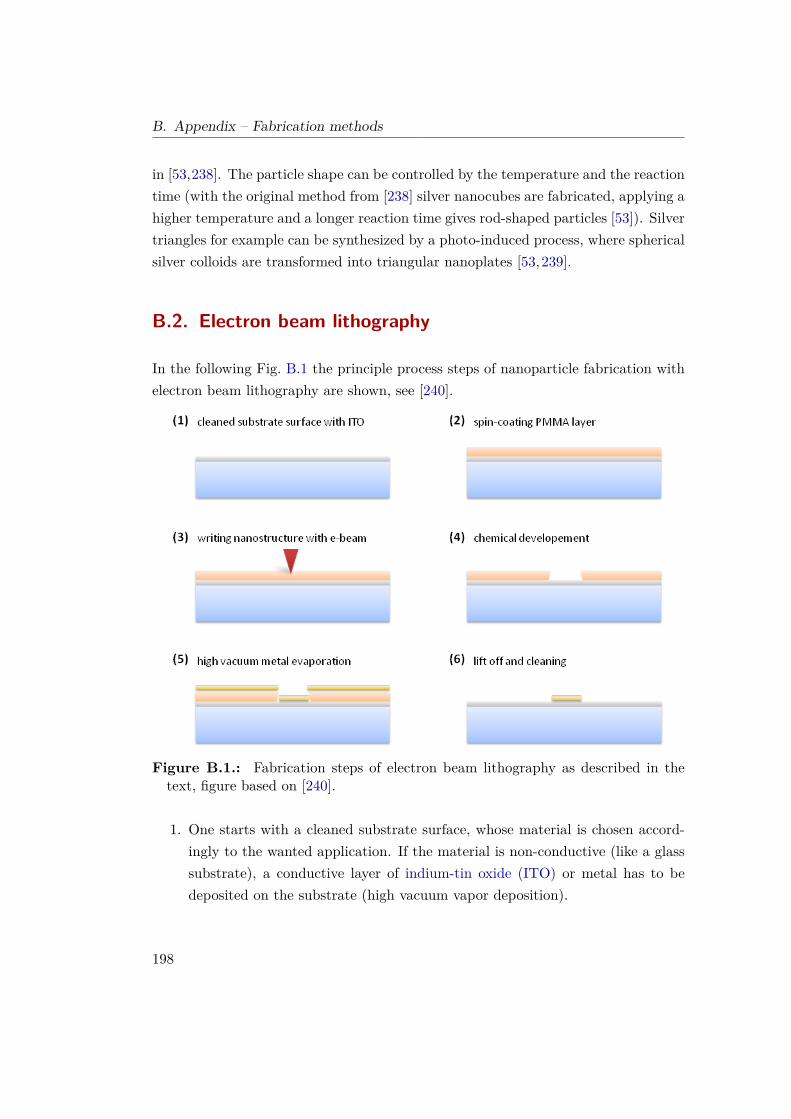
B. Appendix – Fabrication methods
in [53,238]. The particle shape can be controlled by the temperature and the reactiontime (with the original method from [238] silver nanocubes are fabricated, applying ahigher temperature and a longer reaction time gives rod-shaped particles [53]). Silvertriangles for example can be synthesized by a photo-induced process, where sphericalsilver colloids are transformed into triangular nanoplates [53, 239].
B.2. Electron beam lithography
In the following Fig. B.1 the principle process steps of nanoparticle fabrication withelectron beam lithography are shown, see [240].
Figure B.1.: Fabrication steps of electron beam lithography as described in thetext, figure based on [240].
1. One starts with a cleaned substrate surface, whose material is chosen accord-ingly to the wanted application. If the material is non-conductive (like a glasssubstrate), a conductive layer of indium-tin oxide (ITO) or metal has to bedeposited on the substrate (high vacuum vapor deposition).
198

B.2. Electron beam lithography
2. In a spin-coat process a typically 100 nm thick layer of PMMA is put on thestructure. This layer is a positive electron resist and has to be baked on aheating plate at 170 for 8 hours [240].
3. The PMMA layer is exposed by an electron beam and the desired nanoparticlestructure is written.
4. After the electron beam exposure the resist layer is chemically developed.(Starting with a developer bath for 30 s, immediately followed by a chemi-cal stopper bath for 30 s and an isopropanol rinsing step [240].)
5. After cleaning, the nanoparticle metal (e.g. gold) is deposited in a high vacuumevaporation process.
6. An acetone bath is used to remove the remaining PMMA layer resist.
7. To finish the fabrication process, the surface is cleaned with a final isopropanolrinsing.
The resulting particles are polycrystalline and their surface roughness is higher thanfor chemical synthesized particles (also see Chap. 6). Thermal annealing could helpto reduce the roughness and leads to reduced damping, an increasing absorption andthe FWHM becomes narrower, see [237].
199


C. Appendix – MATLAB
C.1. MATLAB memory limitations for different operatingsystems
Operating system and software platform Process Limit32-bit Windows 7, XP and Vista 2 GB32-bit Windows XP, Vista with 3 GB switch 3 GB32-bit Linux ~ 3 GB64-bit Operating system running 32-bit Matlab® ≤ 4 GB64-bit Operating system running 64-bit Matlab® 8 TB
Table C.1.: Memory characteristics and limitations for different Matlab® platformsand operating systems. The process limit is the maximum amount of virtualmemory a single process (or application) can address – on 32-bit systems, this isthe most important factor limiting data set size. The Matlab® memory functionallows to verify the current process limit on Windows systems. Data and tableadopted from Matlab® Product Support 1107, Avoiding ’Out of Memory’ Errors,http://www.mathworks.com/support/tech-notes/1100/1107.html.
201

C. Appendix – MATLAB
Operatingsystem andconfiguration
Total workspacesize
Largest matrixsize
Number ofElements inlargest realdouble array
Number ofelements inlargest int8
array
32-bit WindowsXP
~1700 MB ~1189 MB ~155× 106 ~1246× 106
32-bit WindowsVista
~1643 MB ~1428 MB ~187× 106 ~1497× 106
32-bit WindowsXP, best case,
with 3GB switch
~2700 MB ~1536 MB ~200× 106 ~1610× 106
32-bit Linux ~2683 MB ~2385 MB ~312× 106 231 − 2(~2147× 106)
MAC OS Xrunning 32-bit
Matlab®
~2919 MB ~1532 MB ~200× 106 ~1606× 106
64-bit WindowsXP running
32-bit Matlab®
~3155 MB ~2047 MB ~268× 106 231 − 2(~2147× 106)
64-bit Linuxrunning 32-bit
Matlab®
~3558 MB ~2292 MB ~300× 106 231 − 2(~2147× 106)
Solaris running32-bit Matlab®
~3535 MB ~3072 MB ~402× 106 231 − 2(~2147× 106)
64-bit OSrunning 64-bitMatlab® 7.4and earlier
~< 8 TB 16 GB (doublearray) / 2GB(int8 array)
231 − 2(~2147× 106)
231 − 2(~2147× 106)
64-bit OSrunning 64-bitMatlab® 7.5and later
~< 8TB < 8 TB 248 − 1(~2.8× 10¹⁴)
248 − 1(~2.8× 10¹⁴)
Table C.2.: Largest (real double) matrix and total workspace size for differentplatforms. Table adopted from Matlab® Product Support 1110, Maximum Ma-trix Size by Platform, http://www.mathworks.com/support/tech-notes/1100/1110.html.
202

C.2. MATLAB script for Mie solution
C.2. MATLAB script for Mie solution
With the following code example the scattering, absorption and extinction crosssection for a spherical particle of arbitrary size can be calculated. The dielectric datafor the sphere has to be provided, viz. [41]1.
1 % MATLAB code for Mie solution of Maxwell's equations.
2 %
3 % written by U. Hohenester and A. Truegler
4 % Karl−Franzens−University Graz, Austria
5 % contact: ulrich.hohenester@uni−graz.at6
7 % diameter of sphere in nm
8 diameter = 50;
9 % energy range in nm
10 enei = linspace( 300, 800, 201 );
11
12 % background dielectric function and refractive index
13 nb = 1.34; epsb = nb ^ 2;
14 % dielectric function of particle (e.g. data from Johnson & Christy)
15 epsin = epstable( 'gold.dat' );
16 % ratio of dielectric functions
17 epsz = epsin( enei ) / epsb;
18
19 % wavevector of light
20 k = 2 * pi ./ enei * nb;
21
22 % preallocate memory for cross sections
23 sca = zeros( size( enei ) ); ext = zeros( size( enei ) );
24
25 % table of spherical harmonic degrees, lmax = max. number of degrees
26 ltab = []; lmax = 50;
27 for i = 1 : lmax
28 ltab = [ ltab; i * ones( 3, 1 ) ];
29 end
30 [ l, ind ] = unique( ltab ); % find unique values
31
1Remember that usually the real and imaginary part of the refractive index n = n +ik is givenand therefore <eε = n2 − k2 and =mε = 2nk.
203

C. Appendix – MATLAB
32 % calculate scattering and extinction cross section
33 for i = 1 : length( enei )
34 % Mie coefficients
35 [ a, b ] = miecoefficients( k( i ), diameter, epsz( i ), 1, ltab );
36 % scattering cross section
37 sca( i ) = 2 * pi / k( i ) ^ 2 * ...
38 ( 2 * l' + 1 ) * ( abs( a( ind ) ) .^ 2 + abs( b( ind ) ) .^ 2 );
39 % extinction cross section
40 ext( i ) = 2 * pi / k( i ) ^ 2 * ...
41 ( 2 * l' + 1 ) * real( a( ind ) + b( ind ) );
42 end
43
44 % absorption cross section
45 abs = ext − sca;
46
47 % plot results
48 plot( enei, ext, 'r^−', enei, abs, 'b^−', enei, sca, 'm^−');49 title( 'Mie solution for spherical particle' )
50 legend( 'extinction', 'absorption', 'scattering' );
51 xlabel( 'Photon energy (nm)' );
52 ylabel( 'Cross sections' );
The function miecoefficients.m calculates the Mie coefficients of Eq. (4.10).
1 function [ a, b, c, d ] = miecoefficients( k, diameter, epsr, mur, l )
2 % MIECOEFFICIENTS − Mie coeff. according to Bohren and Huffman (1983).
3 %
4 % Input
5 % k : wavevector of light outside of sphere
6 % diameter : diameter of sphere
7 % epsr : dielectric constant of sphere
8 % mur : magnetic permeability of sphere
9 % l : angular momentum components
10 % Output
11 % Mie coefficients a, b, c, d
12
13 % refractive index
14 nr = sqrt( epsr * mur );
15
16 % compute Riccati−Bessel functions
204

C.2. MATLAB script for Mie solution
17 [ j1, h1, zjp1, zhp1 ] = riccatibessel( nr * k * diameter / 2, l );
18 [ j2, h2, zjp2, zhp2 ] = riccatibessel( k * diameter / 2, l );
19
20 % Mie coefficients for outside field
21 a = ( nr ^ 2 * j1 .* zjp2 − mur * j2 .* zjp1 ) ./ ...
22 ( nr ^ 2 * j1 .* zhp2 − mur * h2 .* zjp1 );
23 b = ( mur * j1 .* zjp2 − j2 .* zjp1 ) ./ ...
24 ( mur * j1 .* zhp2 − h2 .* zjp1 );
25
26 % Mie coefficients for inside field
27 c = ( mur * j2 .* zhp1 − mur * h2 .* zjp2 ) ./ ...
28 ( mur * j1 .* zhp2 − h2 .* zjp1 );
29 d = ( mur * nr * j2 .* zhp2 − mur * nr * h2 .* zjp1 ) ./ ...
30 ( mur ^ 2 * j1 .* zhp1 − mur * h2 .* zjp1 );
The function riccatibessel.m provides the spherical Bessel functions, see Eq. (4.11).
1 function [ j, h, zjp, zhp ] = riccatibessel( z, ltab )
2 % RICCATIBESSEL Riccati−Bessel functions.
3 % Abramowitz and Stegun, Handbook of Math. Functions, Chap. 10.
4 %
5 % INPUT
6 % z ... argument
7 % ltab ... angular momentum components
8 %
9 % OUTPUT
10 % j ... spherical Bessel function of order 1
11 % h ... spherical Bessel function of order 2
12 % zjp ... [ z j( z ) ]'
13 % zhp ... [ z h( z ) ]'
14
15 % unique angular component vector
16 l = 1 : max( ltab );
17
18 % spherical Bessel functions of first and second kind,
19 % see equations (10.1.1) , (10.1.11) , (10.1.12)
20 j0= sin( z )/z; j=sqrt( pi/( 2*z ) )*besselj( l(:)+0.5, z );
21 y0=−cos( z )/z; y=sqrt( pi/( 2*z ) )*bessely( l(:)+0.5, z );
22
23 % spherical Bessel function of third kind (10.1.1)
205

C. Appendix – MATLAB
24 h0 = j0 + 1i * y0; h = j + 1i * y;
25
26 % derivatives (10.1.23), (10.1.24)
27 zjp = z * [ j0; j( 1 : length( l ) − 1 ) ] − l( : ) .* j;
28 zhp = z * [ h0; h( 1 : length( l ) − 1 ) ] − l( : ) .* h;
29
30 % table assignement
31 j = j( ltab ); zjp = zjp( ltab );
32 h = h( ltab ); zhp = zhp( ltab );
206

Bibliography
[1] R. Feynman, “There is plenty of room at the bottom (talk tanscript),”Caltech Engineering and Science 23:5 (1960) 22–36. .
[2] N. Taniguchi, ed., On the Basic Concept of Nano-Technology, Proceedings ofthe International Conference on Production Engineering. Japan Society ofPrecision Engineering, Tokyo, 1974. Part II.
[3] K. E. Drexler, Molecular Machinery and Manufacturing with Applications toComputation. PhD thesis, Massachusetts Institute of Technology (MIT),Cambridge, Massachusetts, 1991. .
[4] L. Novotny and B. Hecht, Principles of Nano-Optics. Cambrigde UniversityPress, UK, 2006, ISBN 978-0521832243. .
[5] H. Atwater, “The promise of plasmonics,” Scientific American 296(4) (2007)56. .
[6] I. H. El-Sayed, X. Huang, and M. A. El-Sayed, “Selective laser photo-thermaltherapy of epithelial carcinoma using anti-EGFR antibody conjugated goldnanoparticles,” Cancer Lett. 239 (2006) 129–135. .
[7] J. N. Anker, W. P. Hall, O. Lyandres, N. C. Shah, J. Zhao, and R. P. V.Duyne, “Biosensing with plasmonic nanosensors,” Nat. Mater. 7 (2008) 442..
[8] A. Haes and R. P. V. Duyne, “A Nanoscale Optical Biosensor: Sensitivity andSelectivity of an Approach Based on the Localized Surface PlasmonResonance Spectroscopy of Triangular Silver Nanoparticles,” J. Am. Chem.Soc. 124 (2002) 10596. .
[9] P. Fortina, L. J. Kricka, D. J. Graves, J. Park, T. Hyslop, F. Tam, N. Halas,S. Surrey, and S. A. Waldman, “Applications of nanoparticles to diagnosticsand therapeutics in colorectal silver nanoparticles,” JACS 124 (2007) 10596..
[10] J. B. Pendry, “Negative refraction makes a perfect lense,” Phys. Rev. Lett. 85(2000) 3966. .
207

BIBLIOGRAPHY
[11] H. J. Lezec, J. A. Dionne, and H. A. Atwater, “Negative refraction at visiblefrequencies,” Science 316 (2007) 5823. .
[12] N. I. Zheludev, “A Roadmap for Metamaterials,” Opt. Photonics News 22(2011) 30–35. .
[13] P. Zijlstra, J. M. Chon, and M. Gu, “Five-dimensional optical recordingmediated by surface plasmons in gold nanorods,” Nat. 459 (2009) 410–413..
[14] B. Lamprecht, J. R. Krenn, G. Schider, H. Ditlbacher, M. Salerno, N. Felidj,A. Leitner, F. R. Aussenegg, and J. C. Weeber, “Surface plasmon propagationin microscale metal stripes,” Appl. Phys. Lett. 79 (2001) 51. .
[15] S. I. Bozhevolnyi, V. S. Volkov, E. Deveaux, J. Y. Laluet, and T. W.Ebbensen, “Channel plasmon subwavelength waveguide components includinginterferometers and ring resonators,” Nature 440 (2006) 509. .
[16] A. Akimov, A. Mukherjee, C. L. Yu, D. E. Chang, A. S. Zibrov, P. R.Hemmer, H. Park, and M. D. Lukin, “Generation of single optical plasmons inmetallic nanowires coupled to quantum dots,” Nat. 450 (2007) 402–406. .
[17] R. Kolesov, B. Grotz, G. Balasubramanian, R. J. Stöhr, A. A. L. Nicolet,P. R. Hemmer, F. Jelezko, and J. Wachtrup, “Wave-particle duality of singlesurface plasmon polaritons,” Nat. Phys. 5 (2009) 470–474. .
[18] D. M. Koller, A. Hohenau, H. Ditlbacher, N. Galler, F. Reil, F. R. Aussenegg,A. Leitner, E. J. W. List, and J. R. Krenn, “Organic plasmon-emittingdiode,” Nat. Phot. 2 (2008) 684–687. .
[19] A. L. Falk, F. H. L. Koppens, C. L. Yu, K. Kang, N. de Leon Snapp, A. V.Akimov, M.-H. Jo, M. D. Lukin, and H. Park, “Near-field electrical detectionof optical plasmons and single-plasmon sources,” Nat. Phys. 5 (2009)475–479. .
[20] V. E. Ferry, L. A. Sweatlock, D. Pacifici, and H. A. Atwater, “PlasmonicNanostructure Design for Efficient Light Coupling into Solar Cells,” NanoLett. 8 (2008) 4391. .
[21] H. Raether, Surface Plasmons on Smooth and Rough Surfaces and onGratings, vol. 111 of Springer Tracts in Modern Physics. Springer-Verlag,Berlin, 1988, ISBN 978-0387173634. .
[22] H. Raether, Excitation of Plasmons and Interband Transitions by Electrons,vol. 88 of Springer Tracts in Modern Physics. Springer-Verlag, Berlin, 1980,ISBN 978-3540096771. .
208

BIBLIOGRAPHY
[23] F. J. García de Abajo, “Optical excitations in electron microscopy,” Rev.Mod. Phys. 82 (2010) 209. .
[24] J. Dostálek, J. Homola, S. Jiang, J. Ladd, S. Löfås, A. McWhirter, D. G.Myszka, I. Navratilova, M. Piliarik, J. Štěpánek, A. Taylor, andH. Vaisocherová, Surface Plasmon Resonance Based Sensors. Springer Serieson Chemical Sensors and Biosensors. Springer-Verlag, Berlin Heidelberg,2006, ISBN 978-3642070464. .
[25] R. W. Wood, “On a remarkable case of uneven distribution of light in adiffraction grating spectrum,” Philosophical Magazine 4 no. 21, (1902)396–402. .
[26] L. Rayleigh, “On the Dynamical Theory of Gratings,” Proc. R. Soc. Lond. A79 no. 532, (1907) 399–416. .
[27] R. B. Schasfoort and A. J. Tudos, eds., Handbook of Surface PlasmonResonance. The Royal Society of Chemistry, 2008, ISBN 978-0854042678. .
[28] U. Fano, “The Theory of Anomalous Diffraction Gratings and ofQuasi-Stationary Waves on Metallic Surfaces (Sommerfeld’s Waves),” J. Opt.Soc. Am. 31 (1941) 213–222. .
[29] R. Ritchie, “Plasma Losses by Fast Electrons in Thin Films,” Phys. Rev. 106no. 5, (1957) 874. .
[30] C. J. Powell and J. B. Swan, “Origin of the Characteristic Electron EnergyLosses in Magnesium,” Phys. Rev. 116 (1959) 81–83. .
[31] C. J. Powell and J. B. Swan, “Effect of Oxidation on the Characteristic LossSpectra of Aluminum and Magnesium,” Phys. Rev. 118 (1960) 640–643. .
[32] T. Turbadar, “Complete Absorption of Light by Thin Metal Films,” Proc.Phys. Soc. 73 no. 1, (1959) 40. .
[33] A. Otto, “Excitation of nonradiative surface plasma waves in silver by themethod of frustrated total reflection,” Zeits. Phys. 216 no. 4, (1968) 398–410..
[34] E. Kretschmann and H. Raether, “Radiative decay of nonradiative surfaceplasmons excited by light,” Z. Naturforsch. A 23 (1968) 2135–2136.
[35] F. H. K. Koppens, D. E. Chang, and F. J. García de Abajo, “Grapheneplasmonics: A platform for strong light-matter interaction,”cond-mat.mes-hall (2011) 1–39, arXiv:1104.2068v1. .
209
BIBLIOGRAPHY
[36] A. Vakil and N. Engheta, “One-Atom-Thick IR Metamaterials andTransformation Optics Using Graphene,” physics.optics (2011) 1–21,arXiv:1101.3585v1. .
[37] P. Drude, “Zur Elektronentheorie der Metalle,” Ann. Phys. 306 no. 3, (1900)566–613. .
[38] P. Drude, “Zur Elektronentheorie der Metalle; II. Teil. Galvanomagnetischeund thermomagnetische Effecte,” Ann. Phys. 3 (1900) 369–402. .
[39] N. W. Ashcroft and N. D. Mermin, Festkörperphysik. Oldenbourg, München,2007, ISBN 978-3-48658273-4. .
[40] F. Ladstädter, U. Hohenester, P. Puschnig, and C. Ambrosch-Draxl,“First-principles caculation of hot-electron scatterings in metals,” Phys. Rev.B 70 (2004) 235125. .
[41] P. B. Johnson and R. W. Christy, “Optical Constants of the Noble Metals,”Phys. Rev. B 6 (1972) 12. .
[42] C. Sönnichsen, Plasmons in metal nanostructures. PhD thesis, Fakultät fürPhysik der Ludwig-Maximilians-Universität München, 2001. .
[43] E. D. Palik, ed., Handbook of Optical Constants of Solids. Academic Press,New York, 1985, ISBN 978-0125444200. .
[44] U. Kreibig and M. Vollmer, Optical Properties of Metal Clusters, vol. 25 ofSpringer Series in Material Science. Springer, Berlin, 1995, ISBN978-3-540-57836-9. .
[45] S. A. Maier, Plasmonics: Fundamentals and Applications. Springer, Berlin,2007, ISBN 978-0-387-33150-8. .
[46] B. Lamprecht, Ultrafast plasmon dynamics in metal nanoparticles. PhDthesis, Institut für Physik, Karl-Franzens-Universität Graz, 2000. .
[47] M. I. Stockman, “Nanoplasmonics: The physics behind the applications,”Physics Today 64 (2011) 39–44. .
[48] M. I. Stockman, “Dark-hot resonances,” Nat. 467 (2010) 541–542. .
[49] U. Leonhardt, “Optical metamaterials: Invisibility cup,” Nat. Phot. 1 (2007)207–208. .
[50] H. Tait, ed., Five Thousand Years of Glass. University of Pennsylvania Press,2004, revised edition, ISBN 978-0-8122-1888-6. .
210

BIBLIOGRAPHY
[51] J. Pérez-Juste, I. Pastoriza-Santos, L. M. Liz-Marzán, and P. Mulvaney,“Gold nanorods: Synthesis, characterization and applications,” Coord. Chem.Rev. 249 (2005) 1870–1901. .
[52] S. K. Mitra, N. Dass, , and N. C. Varshneya, “Temperature Dependence ofthe Refractive Index of Water,” J. Chem. Phys. 57 (1972) 1798. .
[53] J. Becker, Plasmons as Sensors. PhD thesis, Fachbereich Chemie, Pharmazieund Geowissenschaften der Johannes-Gutenberg Universität Mainz, 2010. .
[54] A. Ohlinger, S. Nedev, A. A. Lutich, and F. J., “Optothermal Escape ofPlasmonically Coupled Silver Nanoparticles from a Three-DimensionalOptical Trap,” Nano Lett. 11 (2010) 1770. .
[55] S. Gerber, F. Reil, U. Hohenester, T. Schlagenhaufen, J. R. Krenn, andA. Leitner, “Tailoring light emission properties of fluorophores by coupling toresonance–tuned metallic nanostructures,” Phys. Rev. B 75 (2007) 073404..
[56] U. Hohenester and A. Trügler, “Interaction of single molecules with metallicnanoparticles,” IEEE Journal of Selected Topics in Quantum Electronics 14(2008) 1430. .
[57] A. Kinkhabwala, Z. Yu, S. Fan, Y. Avlasevich, K. Müllen, and W. E.Moerner, “Large single-molecule fluorescence enhancements produced by abowtie nanoantenna,” Nat. Phot. 3 (2009) 654–657. .
[58] M. A. Cooper, “Optical biosensors in drug discovery,” Nat. Rev. DrugDiscovery 1 (2002) 515–528. .
[59] H. A. Atwater and A. Polman, “Plasmonics for improved photovoltaicdevices,” Nat. Mat. 9 (2010) 205–213. .
[60] V. Myroshnychenko, J. Rodríguez-Fernández, I. Pastoriza-Santos, A. M.Funston, C. Novo, P. Mulvaney, L. M. Liz-Marzán, and F. J. G. de Abajo,“Modelling the optical response of gold nanoparticles,” Chem. Soc. Rev. 37(2008) 1792–1805. .
[61] J.-S. Huang, J. Kern, P. Geisler, P. Weinmann, M. Kamp, A. Forchel,P. Biagioni, and B. Hecht, “Mode Imaging and Selection in Strongly CoupledNanoantennas,” Nano Lett. 10 (2010) 2105. .
[62] C.-K. Sun, F. Vallée, L. H. Acioli, E. P. Ippen, and J. G. Fujimoto,“Femtosecond-tunable measurement of electron thermalization in gold,” Phys.Rev. B 50 (1994) 15337–15348. .
211

BIBLIOGRAPHY
[63] M. Wolf, “Femtosecond dynamics of electronic excitations at metal surfaces,”Surf. Scie. 377-379 (1997) 343–349. .
[64] M. Burresi, D. van Oosten, T. Kampfrath, H. Schoenmaker, R. Heideman,A. Leinse, and L. Kuipers, “Probing the Magnetic Field of Light at OpticalFrequencies,” Science 326 (2009) 550–553. .
[65] H. Giessen and R. Vogelgesang, “Glimpsing the Weak Magnetic Field ofLight,” Science 23 (2009) 529–530. .
[66] J. D. Jackson, Classical Electrodynamics. Wiley, New York, 1962, ISBN978-0-471-30932-1. .
[67] W. Thirring, Lehrbuch der Mathematischen Physik - Band 2 KlassischeFeldtheorie. Springer, Wien, New York, 1989, ISBN 978-3211821695. .
[68] E. T. Whittaker, A history of the theories of aether and electricity: from theage of Descartes to the close of the nineteenth century. University ofCalifornia Libraries, 2011 (1910), ISBN 978-1125241103. .
[69] C. Cohen-Tannoudji, J. Dupont-Roc, and G. Grynberg, Photons and Atoms –Introduction to Quantum Electrodynamics. Wiley-VCH, New York, 1997,ISBN 978-0-471-18433-1. .
[70] E. Altewischer, W. P. van Exter, and J. P. Woerdman, “Plasmon-assistedtransmission of entangled photons,” Nat. 418 (2002) 304–306. .
[71] M. O. Scully and M. S. Zubairy, Quantum Optics. Cambridge UniversityPress, UK, 1997, ISBN 978-0521435956. .
[72] J. Zuloaga, E. Prodan, and P. Nordlander, “Quantum Description of thePlasmon Resonances of a Nanoparticle Dimer,” Nano Lett. 9 (2009) 887–891..
[73] S. J. Plimpton and W. E. Lawton, “A Very Accurate Test of Coulomb’s Lawof Force Between Charges,” Phys. Rev. 50 (1936) 1066–1071. .
[74] R. Lakes, “Experimental Limits on the Photon Mass and Cosmic MagneticVector Potential,” Phys. Rev. Lett. 80 (1998) 1826–1829. .
[75] D. L. Mills, Nonlinear Optics: Basic Concepts. Springer, Heidelberg, 1998,ISBN 978-3540541929. .
[76] Y. R. Shen, The Principles of Nonlinear Optics. John Wiley & Sons, NewYork, 1984, ISBN 978-0-471-43080-3. .
212

BIBLIOGRAPHY
[77] M. I. Stockman, D. J. Bergman, C. Anceau, S. Brasselet, and J. Zyss,“Enhanced Second-Harmonic Generation by Metal Surfaces with NanoscaleRoughness: Nanoscale Dephasing, Depolarization, and Correlations,” Phys.Rev. Lett. 92 (2004) 057402. .
[78] T. Hanke, G. Krauss, D. Träutlein, B. Wild, R. Bratschitsch, andA. Leitenstorfer, “Efficient Nonlinear Light Emission of Single Gold OpticalAntennas Driven by Few-Cycle Near-Infrared Pulses,” Phys. Rev. Lett. 103(2009) 257404. .
[79] L. V. Lorenz, “On the identity of the vibrations of light with electricalcurrents,” Phil. Mag. 34 (1867) 287–301. .
[80] G. Green, An Essay on the Application of mathematical Analysis to thetheories of Electricity and Magnetism. G. Green, Nothingham, 1828. .Reprinted in Journ. f. Math. in three parts, digitized version available byGoogle books.
[81] D. M. Cannell and N. J. Lord, “George Green, Mathematician and Physicist1793–1841,” The Mathematical Gazette 77 no. 478, (1993) 26–51. .
[82] F. J. García de Abajo and A. Howie, “Retarded field calculation of electronenergy loss in inhomogeneous dielectrics,” Phys. Rev. B 65 (2002) 115418. .
[83] U. Hohenester and J. Krenn, “Surface plasmon resonances of single andcoupled metallic nanoparticles: A boundary integral method approach,” Phys.Rev. B 72 (2005) 195429. .
[84] U. Hohenester, Matlab® help for MNPBEM toolbox. Institut für Physik,Karl–Franzens–Universität Graz, 2011. .
[85] R. Fuchs, “Theory of the optical properties of ionic crystal cubes,” Phys. Rev.B 11 (1975) 1732. .
[86] I. D. Mayergoyz, Z. Zhang, and G. Miano, “Analysis of Dynamics ofExcitation and Dephasing of Plasmon Resonance Modes in Nanoparticles,”Phys. Rev. Lett. 98 (2007) 147401. .
[87] A. Messiah, Quantum Mechanics. North-Holland, Amsterdam, 1965, ISBN978-0486409245. .
[88] U. Hohenester and A. Trügler, “MNPBEM – A Matlab toolbox for thesimulation of plasmonic nanoparticles,” Comp. Phys. Commun. 183 (2012)370. .
213

BIBLIOGRAPHY
[89] R. G. Newton, “Optical Theorem and Beyond,” Am. J. Phys. 44 (1976)639–642. .
[90] H. C. van de Hulst, Light Scattering by Small Particles. Dover Publications,New York, 1981, ISBN 978-0486642284. .
[91] U. Kreibig, “Hundert Jahre Mie-Theorie,” Phys. Unserer Zeit 39 no. 6,(2008) 281–287. .
[92] G. Mie, “Beiträge zur Optik trüber Medien, speziell kolloidalerMetalllösungen,” Ann. Phys. 330 no. 3, (1908) 377–445. .
[93] C. F. Bohren and D. R. Huffman, Absorption and scattering of light by smallparticles. Wiley-Interscience, 1983, ISBN 978-0471293408. .
[94] J. A. Stratton, Electromagnetic Theory. Wiley-IEEE Press, 2007, ISBN978-0-470-13153-4. .
[95] B. T. Draine and P. J. Flatau, “Discrete-dipole approximation for scatteringcalculations,” J. Opt. Soc. Am. A 11 no. 4, (1994) 1491. .
[96] B. T. Draine and P. J. Flatau, “User Guide to the Discrete DipoleApproximation Code DDSCAT 7.1,” astro-ph.IM (2010) 1–83,arXiv:1002.1505v1. .
[97] B. Draine, “The Discrete-Dipole Approximation and its Application toInterstellar Graphite Grains,” Astrophys. J. 333 (1988) 848–872. .
[98] H. A. Lorentz, The Theory of Electrons and its Applications to thePhenomena of Light and Radiant Heat. Teubner, Leipzig, 1909. .
[99] E. M. Purcell and C. R. Pennypacker, “Scattering and absorption of light bynonspherical dielectric grains,” Astrophys. J. 186 (1973) 705–714. .
[100] A. Sutradhar, G. H. Paulino, and L. J. Gray, Symmetric Galerkin BoundaryElement Method. Springer-Verlag, Berlin Heidelberg, 2008, ISBN978-3-540-68770-2. .
[101] M. A. Yurkin and A. G. Hoekstra, “The discrete dipole approximation: Anoverview and recent developments,” J. Quant. Spectrosc. Radiat. Transf. 106(2007) 558–589. Also available at arXiv:0704.0038v1. .
[102] T. Wriedt and U. Comberg, “Comparison of computational scatteringmethods,” J. Quant. Spectrosc. Radiat. Transf. 60 no. 3, (1998) 411–423. .
214

BIBLIOGRAPHY
[103] J. W. Hovenier, K. Lumme, M. I. Mishchenko, N. V. Voshchinnikov, D. W.Mackowski, and J. Rahola, “Computations of scattering matrices of fourtypes of non-spherical particles using diverse methods,” J. Quant. Spectrosc.Radiat. Transf. 55 no. 6, (1996) 695–705. .
[104] U. Kreibig, “Interface-induced dephasing of Mie plasmon polaritons,” App.Phys. B 93 (2008) 79–89. .
[105] L. Rayleigh, “On the theory of optical images, with special reference to themicroscope,” Philos. Mag. 42 (1896) 167–195. .
[106] E. Abbe, “Beiträge zur Theorie des Mikroskops und der mikroskopischenWahrnehmung,” Archiv für Mikroskopische Anatomie 9 no. 1, (1873) 413–418..
[107] M. Bosman, V. J. Keast, M. Watanabe, A. I. Maaroof, and M. B. Cortie,“Mapping surface plasmons at the nanometre scale with an electron beam,”Nanotechnology 18 (2007) 165505. .
[108] J. Nelayah, M. Kociak, O. Stephan, F. J. García de Abajo, M. Tence,L. Henrard, D. Taverna, I. Pastoriza-Santos, L. M. Liz-Martin, andC. Colliex, “Mapping surface plasmons on a single metallic nanoparticle,”Nat. Phys. 3 (2007) 348. .
[109] R. H. Ritchie and A. Howie, “Inelastic scattering probabilities in scanningtransmission electron microscopy,” Philos. Mag. A 58 no. 5, (1988) 753–767..
[110] U. Hohenester, H. Ditlbacher, and J. R. Krenn, “Electron-Energy-LossSpectra of Plasmonic Nanoparticles,” Phys. Rev. Lett. 103 (2009) 106801. .
[111] F. J. García de Abajo and M. Kociak, “Probing the Photonic Local Densityof States with Electron Energy Loss Spectroscopy,” Phys. Rev. Lett. 100(2008) 106804. .
[112] J. M. McMahon, S. K. Gray, and G. C. Schatz, “Nonlocal Optical Responseof Metal Nanostructures with Arbitrary Shape,” Phys. Rev. Lett. 103 (2009)097403. .
[113] M. Z. Maialle, E. A. de Andrada e Silva, and L. J. Sham, “Exciton spindynamics in quantum wells,” Phys. Rev. B 47 (1993) 15 776. .
[114] P. S. Pershan, “Nonlinear Optical Properties of Solids: EnergyConsiderations,” Phys. Rev. 130 (1963) 919–929. .
215

BIBLIOGRAPHY
[115] E. Adler, “Nonlinear Optical Frequency Polarization in a Dielectric,” Phys.Rev. 134 (1964) A728–A733. .
[116] M. Lippitz, M. A. van Dijk, and M. Orrit, “Third-Harmonic Generation fromSingle Gold Nanoparticles,” Nano Lett. 5 (2005) 799–802. .
[117] B. K. Canfield, H. Husu, J. Laukkanen, B. Bai, M. Kuittinen, J. Turunen, andM. Kauranen, “Local Field Asymmetry Drives Second-Harmonic Generationin Noncentrosymmetric Nanodimers,” Nano Lett. 7 (2007) 1251–1255. .
[118] J. E. Sipe, D. J. Moss, and H. M. van Driel, “Phenomenological theory ofoptical second- and third-harmonic generation from cubic centrosymmetriccrystals,” Phys. Rev. B 35 (1987) 1129–1141. .
[119] N. Bloembergen, W. K. Burns, and M. Matsouka, “Reflected third harmonicgenerated by picosecond laser pulses,” Opt. Commun. 1 (1969) 195–198. .
[120] U. Gubler and C. Bosshard, “Optical third-harmonic generation of fused silicain gas atmosphere: Absolute value of the third-order nonlinear opticalsusceptibility χ(3),” Phys. Rev. B 61 (2000) 10702–10710. .
[121] F. Krausz and E. Wintner, “Atmospheric influences in optical third-harmonicgeneration experiments,” App. Phys. B 49 (1989) 479–483. .
[122] P. K. Jain, W. Y. Huang, and M. A. El-Sayed, “On the universal scalingbehavior of the distance decay of plasmon coupling in metal nanoparticlepairs: a plasmon ruler equation,” Nano Lett. 7 (2007) 2080–2088. .
[123] C. Sönnichsen, B. Reinhard, J. Liphardt, and A. Alivisatos, “A molecularruler based on plasmon coupling of single gold and silver nanoparticles,” Nat.Biotechnol. 23 (2005) 741–745. .
[124] H. Wang and B. M. Reinhard, “Monitoring Simultaneous Distance andOrientation Changes in Discrete Dimers of DNA Linked Gold Nanoparticles,”J. Phys. Chem. C 113 (2009) 11215–11222. .
[125] B. M. Reinhard, M. Siu, H. Agarwal, A. P. Alivisatos, and J. Liphardt,“Calibration of Dynamic Molecular Rulers Based on Plasmon Couplingbetween Gold Nanoparticles,” Nano Lett. 5 (2005) 2246–2252. .
[126] C. Sönnichsen and A. P. Alivisatos, “Gold Nanorods as Novel NonbleachingPlasmon-Based Orientation Sensors for Polarized Single-Particle Microscopy,”Nano Lett. 5 (2005) 301–304. .
216
BIBLIOGRAPHY
[127] J. M. Bingham, K. A. Willets, N. C. Shah, A. D. Q., and R. P. Van Duyne,“Localized Surface Plasmon Resonance Imaging: Simultaneous SingleNanoparticle Spectroscopy and Diffusional Dynamics,” J. Phys. Chem. C 113(2009) 16839–16842. .
[128] S. Pierrat, E. Hartinger, S. Faiss, A. Janshoff, and C. Sönnichsen, “RotationalDynamics of Laterally Frozen Nanoparticles Specifically Attached toBiomembranes,” J. Phys. Chem. C 113 (2009) 11179–11183. .
[129] O. Schubert, J. Becker, L. Carbone, Y. Khalavka, T. Provalska, I. Zins, andC. Sönnichsen, “Mapping the Polarization Pattern of Plasmon Modes RevealsNanoparticle Symmetry,” Nano Lett. 8 (2008) 2345–2350. .
[130] C. Novo, A. M. Funston, and P. Mulvaney, “Direct observation of chemicalreactions on single gold nanocrystals using surface plasmon spectroscopy,”Nat. Nanotechnol. 3 (2008) 598–602. .
[131] L. Carbone, A. Jakab, Y. Khalavka, and C. Sönnichsen, “Light-ControlledOne-Sided Growth of Large Plasmonic Gold Domains on Quantum RodsObserved on the Single Particle Level,” Nano Lett. 9 (2009) 3710–3714. .
[132] J. Homola, S. S. Yee, and G. Gauglitz, “Surface plasmon resonance sensors:review,” Sens. Actuat. B Chem. 54 (1999) 3–15. .
[133] C. Sönnichsen, S. Geier, N. E. Hecker, G. von Plessen, J. Feldmann,H. Ditlbacher, B. Lamprecht, J. R. Krenn, F. R. Aussenegg, V. Z. H. Chan,J. P. Spatz, and M. Moller, “Spectroscopy of single metallic nanoparticlesusing total internal reflection microscopy,” Appl. Phys. Lett. 77 (2000)2949–2951. .
[134] G. Raschke, S. Kowarik, T. Franzl, C. Sönnichsen, T. A. Klar, J. Feldmann,A. Nichtl, and K. Kürzinger, “Biomolecular Recognition Based on Single GoldNanoparticle Light Scattering,” Nano Lett. 3 (2003) 935–938. .
[135] C. Sönnichsen, T. Franzl, T. Wilk, G. von Plessen, and J. Feldmann, “DrasticReduction of Plasmon Damping in Gold Nanorods,” Phys. Rev. Lett. 88(2002) 077402. .
[136] J. Becker, O. Schubert, and C. Sönnichsen, “Gold Nanoparticle GrowthMonitored in situ Using a Novel Fast Optical Single-Particle SpectroscopyMethod,” Nano Lett. 7 (2007) 1664–1669. .
[137] A. D. McFarland and R. P. Van Duyne, “Single Silver Nanoparticles asReal-Time Optical Sensors with Zeptomole Sensitivity,” Nano Lett. 3 (2003)1057–1062. .
217

BIBLIOGRAPHY
[138] C. L. Baciu, J. Becker, A. Janshoff, and C. Sönnichsen, “Protein-MembraneInteraction Probed by Single Plasmonic Nanoparticles,” Nano Lett. 8 (2008)1724–1728. .
[139] K. S. Lee and M. A. El-Sayed, “Gold and Silver Nanoparticles in Sensing andImaging: Sensitivity of Plasmon Response to Size, Shape, and MetalComposition,” J. Phys. Chem. B 110 (2006) 19220–19225. .
[140] Y. Khalavka, J. Becker, and C. Sönnichsen, “Synthesis of Rod-Shaped GoldNanorattles with Improved Plasmon Sensitivity and Catalytic Activity,” J.Am. Chem. Soc. 131 (2009) 1871–1875. .
[141] N. Liu, T. Weiss, M. Mesch, L. Langguth, U. Eigenthaler, M. Hirscher,C. Sönnichsen, and H. Giessen, “Planar Metamaterial Analogue ofElectromagnetically Induced Transparency for Plasmonic Sensing,” NanoLett. 10 (2010) 1103–1107. .
[142] J. Becker, I. Zins, A. Jakab, Y. Khalavka, O. Schubert, and C. Sönnichsen,“Plasmonic Focusing Reduces Ensemble Linewidth of Silver-Coated GoldNanorods,” Nano Lett. 8 (2008) 1719–1723. .
[143] J. Burgin, M. Z. Liu, and P. Guyot-Sionnest, “Dielectric Sensing withDeposited Gold Bipyramids,” J. Phys. Chem. C 112 (2008) 19279–19282. .
[144] L. J. Sherry, S. H. Chang, G. C. Schatz, R. P. Van Duyne, B. J. Wiley, andY. N. Xia, “Localized Surface Plasmon Resonance Spectroscopy of SingleSilver Nanocubes,” Nano Lett. 5 (2005) 2034–2038. .
[145] S. W. Prescott and P. Mulvaney, “Gold nanorod extinction spectra,” J. Appl.Phys. 99 (2006) 123504. .
[146] G. W. Bryant, F. J. García de Abajo, and J. Aizpurua, “Mapping thePlasmon Resonances of Metallic Nanoantennas,” Nano Lett. 8 (2008)631–636. .
[147] M. Z. Liu and P. Guyot-Sionnest, “Synthesis and Optical Characterization ofAu/Ag Core/Shell Nanorods,” J. Phys. Chem. B 108 (2004) 5882–5888. .
[148] J. A. Osborn, “Demagnetizing Factors of the General Ellipsoid,” Phys. Rev.67 (1945) 351–357. .
[149] A. Lambrecht, I. Pirozhenko, L. Duraffourg, and P. Andreucci, “The Casimireffect for silicon and gold slabs,” EPL 77 (2007) 44006. .
218

BIBLIOGRAPHY
[150] M. Cao, M. Wang, and N. Gu, “Optimized Surface Plasmon ResonanceSensitivity of Gold Nanoboxes for Sensing Applications,” J. Phys. Chem. C113 (2009) 1217–1221. .
[151] B. Nikoobakht and M. A. El-Sayed, “Preparation and Growth Mechanism ofGold Nanorods (NRs) Using Seed-Mediated Growth Method,” Chem. Mater.15 (2003) 1957–1962. .
[152] K. M. Mayer, F. Hao, S. Lee, P. Nordlander, and J. H. Hafner, “A singlemolecule immunoassay by localized surface plasmon resonance,” Nanotechnol.21 (2010) 255503. .
[153] C. L. Wu and Q. H. Xu, “Stable and Functionable Mesoporous Silica-CoatedGold Nanorods as Sensitive Localized Surface Plasmon Resonance (LSPR)Nanosensors,” Langmuir 25 (2009) 9441–9446. .
[154] M. A. Otte, B. Sepúlveda, W. H. Ni, J. Pérez-Juste, L. M. Liz-Marzán, andL. M. Lechuga, “Identification of the Optimal Spectral Region for Plasmonicand Nanoplasmonic Sensing,” ACS Nano 4 (2010) 349–357. .
[155] K. L. Kelly, E. Coronado, L. L. Zhao, and G. C. Schatz, “The OpticalProperties of Metal Nanoparticles: The Influence of Size, Shape, andDielectric Environment,” J. Phys. Chem. B 107 (2003) 668–677. .
[156] J. Becker, A. Trügler, A. Jakab, U. Hohenester, and C. Sönnichsen, “Theoptimal aspect ratio of gold nanorods for plasmonic bio-sensing,” Plasmonics5 (2010) 161. .
[157] M. A. Mahmoud and M. A. El-Sayed, “Gold Nanoframes: Very High SurfacePlasmon Fields and Excellent Near-Infrared Sensors,” J. Am. Chem. Soc. 132(2010) 12704–12710. .
[158] L. M. Liz-Marzán, “Tailoring Surface Plasmons through the Morphology andAssembly of Metal Nanoparticles,” Langmuir 22 (2006) 32–41. .
[159] P. K. Jain and M. A. El-Sayed, “Noble Metal Nanoparticle Pairs: Effect ofMedium for Enhanced Nanosensing,” Nano Lett. 8 (2008) 4347–4352. .
[160] E. Ringe, J. M. McMahon, K. Sohn, C. Cobley, Y. N. Xia, J. X. Huang, G. C.Schatz, L. D. Marks, and R. P. Van Duyne, “Unraveling the Effects of Size,Composition, and Substrate on the Localized Surface Plasmon ResonanceFrequencies of Gold and Silver Nanocubes: A Systematic Single-ParticleApproach,” J. Phys. Chem. C 114 (2010) 12511–12516. .
219

BIBLIOGRAPHY
[161] H. Wei, A. Reyes-Coronado, P. Nordlander, J. Aizpurua, and H. X. Xu,“Multipolar Plasmon Resonances in Individual Ag Nanorice,” ACS Nano 4(2010) 2649–2654. .
[162] M. D. Malinsky, K. L. Kelly, G. C. Schatz, and R. P. Van Duyne,“Nanosphere lithography: Effect of the substrate on the localized surfaceplasmon resonance spectrum of silver nanoparticles,” J. Phys. Chem. B 105(2001) 2343–2350. .
[163] B. Pietrobon, M. McEachran, and V. Kitaev, “Synthesis of Size-ControlledFaceted Pentagonal Silver Nanorods with Tunable Plasmonic Properties andSelf-Assembly of These Nanorods,” ACS Nano 3 (2009) 21–26. .
[164] A. Unger and M. Kreiter, “Analyzing the Performance of PlasmonicResonators for Dielectric Sensing,” J. Phys. Chem. C 113 (2009)12243–12251. .
[165] J. Sekhon and S. Verma, “Optimal Dimensions of Gold Nanorod forPlasmonic Nanosensors,” Plasmonics 6 (2010) 163–169. .
[166] Y. Tang and M. Ouyang, “Tailoring Properties and Functionalities of MetalNanoparticles through Crystallinity Engineering,” Nat. Mater. 6 (2007)754–759. .
[167] X. C. Jiang and A. B. Yu, “Silver Nanoplates: A Highly Sensitive Materialtoward Inorganic Anions,” Langmuir 24 (2008) 4300–4309. .
[168] N. Cathcart, A. J. Frank, and V. Kitaev, “Silver nanoparticles with planartwinned defects: effect of halides for precise tuning of plasmon resonancemaxima from 400 to > 900 nm,” Chem. Commun. (2009) 7170–7172. .
[169] J. Dorfmüller, R. Vogelgesang, R. T. Weitz, C. Rockstuhl, C. Etrich,T. Pertsch, F. Lederer, and K. Kern, “Fabry-Pérot Resonances inOne-Dimensional Plasmonic Nanostructures,” Nano Lett. 9 (2009) 2372–2377..
[170] M. Schnell, A. García-Etxarri, A. J. Huber, K. Crozier, J. Aizpurua, andR. Hillenbrand, “Controlling the near-field oscillations of loaded plasmonicnanoantennas,” Nat. Phot. 3 (2009) 287–291. .
[171] P. Ghenuche, S. Cherukulappurath, T. H. Taminiau, N. F. van Hulst, andR. Quidant, “Spectroscopic Mode Mapping of Resonant PlasmonNanoantennas,” Phys. Rev. Lett. 101 (2008) 116805. .
220

BIBLIOGRAPHY
[172] B. Schaffer, U. Hohenester, A. Trügler, and F. Hofer, “High-resolution surfaceplasmon imaging of gold nanoparticles by energy-filtered transmissionelectron microscopy,” Phys. Rev. B 79 (2009) 041401(R). .
[173] S. Gerber, F. Reil, U. Hohenester, T. Schlagenhaufen, J. R. Krenn, andA. Leitner, “Tailoring light-emission properties of fluorosphores toresonance-tuned metallic nanostructures,” Phys. Rev. B 75 (2007) 073404. .
[174] P. Anger, P. Bharadwaj, and L. Novotny, “Enhancement and quenching ofsingle–molecule fluorescence,” Phys. Rev. Lett. 96 (2006) 113002. .
[175] S. Kühn, U. Håkanson, L. Rogobete, and V. Sandoghdar, “Enhancement ofSingle-Molecule Fluorescence Using a Gold Nanoparticle as an OpticalNanoantenna,” Phys. Rev. Lett. 97 (2006) 017402. .
[176] B. Lamprecht, G. Schider, R. T. Lechner, H. Ditlbacher, J. R. Krenn,A. Leitner, and F. R. Aussenegg, “Metal Nanoparticle Gratings: Influence ofDipolar Particle Interaction on the Plasmon Resonance,” Phys. Rev. Lett. 84(2000) 4721–4724. .
[177] M. I. J. Stich, S. Nagl, O. Wolfbeis, U. Henne, and M. Schaeferling, “A DualLuminescent Sensor Material for Simultaneous Imaging of Pressure andTemperature on Surfaces,” Adv. Funct. Mater. 18 (2008) 1399. .
[178] E. Ozbay, “Plasmonics: Merging Photonics and Electronics at NanoscaleDimensions,” Science 311 (2006) 189. .
[179] S. Nie and S. R. Emory, “Probing single molecules and single nanoparticles bysurface enhanced Raman scattering,” Science 275 (1997) 1102. .
[180] P. Anger, P. Bharadwaj, and L. Novotny, “Enhancement and Quenching ofSingle-Molecule Fluorescence,” Phys. Rev. Lett. 96 (2006) 113002. .
[181] F. J. Garcia-de Abajo and M. Kociak, “Probing the photonic local density ofstates with electron energy loss spectroscopy,” Phys. Rev. Lett. 100 (2008)106804. .
[182] R. Egerton, “Spatial resolution of nanostructural analysis by electronenergy-loss spectroscopy and energy-filtered imaging,” Journal of ElectronMicroscopy 48 (1999) 711. .
[183] A. Eggeman, P. J. Dobson, and A. K. Petford-Long, “Optical spectroscopyand energy-filtered transmission electron microscopy of surface plasmons incore-shell nanoparticles,” Journal of Applied Physics 101 (2007) 024307. .
221

BIBLIOGRAPHY
[184] W. Grogger, M. Varela, R. Ristau, B. Schaffer, F. Hofer, and K. M. Krishnan,“Energy-filtering transmission electron microscopy on the nanometer lengthscale,” Journal of Electron Spectroscopy and Related Phenomena 143 (2005)139. .
[185] B. Schaffer, G. Kothleitner, and W. Grogger, “EFTEM Spectrum Imaging atHigh Energy Resolution,” Ultramicroscopy 106 (2006) 1129. .
[186] G. Kothleitner and F. Hofer, “EELS performance measurements on a newhigh energy resolution imaging filter,” Micron 34 (2003) 211. .
[187] J. Turkevich, P. C. Stevenson, and J. Hillier, “The size and the shape factorin colloidal systems,” Discussion of the Faraday Society 11 (1951) 9.
[188] G. Kothleitner and B. Schaffer, “Automated EFTEM spectrum imageacquisition: Overcoming EELS dynamic range problems,” Microscopy andMicroanalysis 13 (2007) 156. .
[189] U. Hohenester and J. R. Krenn, “Surface plasmon resonances of single andcoupled metallic nanoparticles: A boundary integral method approach,” Phys.Rev. B 72 (2005) 195429. .
[190] F. J. Garcia de Abajo, “Relativistic energy loss and induced photon emissionin the interaction of a dielectric sphere with an external electron beam,”Phys. Rev. B 59 (1999) 3095. .
[191] B. Schaffer, K. Riegler, G. Kothleitner, W. Grogger, and F. Hofer,“Monochromated, spatially resolved electron energy-loss spectroscopicmeasurements of gold nanoparticles in the plasmon range,” Micron 40 (2008)269–273. .
[192] K. Kimoto, G. Kothleitner, W. Grogger, Y. Matsui, and F. Hofer,“Advantages of a monochromator for bandgap measurements using electronenergy-loss spectroscopy,” Micron 36 (2005) 185. .
[193] J. A. Schuller, E. S. Barnard, W. Cai, Y. C. Jun, J. S. White, and M. L.Brongersma, “Plasmonics for extreme light concentration and manipulation,”Nat. Mater. 9 (2010) 193. .
[194] K. Kneipp, M. Moskovits, and H. Kneipp, eds., Surface-Enhanced RamanScattering, vol. 103 of Topics in Applied Physics. Springer, Heidelberg, NewYork, 2006, ISBN 978-3-540-33566-5. .
[195] D. E. Chang, A. S. Sørensen, P. R. Hemmer, and M. D. Lukin, “QuantumOptics with Surface Plasmons,” Phys. Rev. Lett. 97 (2006) 053002. .
222
BIBLIOGRAPHY
[196] J. B. Pendry, D. Schurig, and D. R. Smith, “Controlling electromagneticfields,” Science 312 (2006) 1780. .
[197] J. Rodríguez-Fernández, A. M. Funston, J. Pérez-Juste, R. A.Álvarez-Puebla, L. M. Liz-Marzán, and P. Mulvaney, “The effect of surfaceroughness on the plasmonic response of individual sub-micron gold spheres,”Phys. Chem. Chem. Phys. 11 (2009) 5909. .
[198] K.-P. Chen, V. P. Drachev, J. D. Borneman, A. V. Kildishev, and V. M.Shalaev, “Drude Relaxation Rate in Grained Gold Nanoantennas,” NanoLett. 10 (2009) 916. .
[199] W. L. Barnes, “Comparing experiment and theory in plasmonics,” J. Opt. A.11 (2009) 114002. .
[200] J. S. Huang, V. Callegari, P. Geisler, C. Brüning, J. Kern, J. Prangsma,P. Weinmann, M. Kamp, A. Forchel, P. Biagioni, U.Sennhauser, andB. Hecht, “Atomically flat single-crystalline gold nanostructures for plasmonicnanocircuitry,” Nat. Comm. 1 (2010) 150. Also available atarXiv:1004.1961v4. .
[201] A. Hohenau, H. Ditlbacher, B. Lamprecht, J. R. Krenn, A. Leitner, and F. R.Aussenegg, “Electron beam lithography: a helpful tool for nanooptics,”Microelec. Engin. 83 (2006) 1464. .
[202] C. Pecharromán, J. Pérez-Juste, G. Mata-Osoro, L. M. Liz-Marzán, andP. Mulvaney, “Redshift of surface plasmon modes of small gold rods due totheir atomic roughness and end-cap geometry,” Phys. Rev. B 77 no. 3, (2008)035418. .
[203] K. Crozier, A. Sundaramurthy, G. Kino, and C. Quate, “Optical antennas:resonators for local field enhancement,” Journ. Appl. Phys. 94 (2003) 4632..
[204] P. Bharadwaj, B. Deutsch, and L. Novotny, “Optical Antennas,” Adv. Opt.Photon. 1 (2009) 438. .
[205] M. Danckwerts and L. Novotny, “Optical Frequency Mixing at Coupled GoldNanoparticles,” Phys. Rev. Lett. 98 (2007) 026104. .
[206] R. Kim et al, “High-harmonic generation by resonant plasmon fieldenhancement,” Nat. 453 (2008) 757. .
223

BIBLIOGRAPHY
[207] K. D. Ko, A. Kumar, K. H. Fung, R. Ambekar, G. L. Liu, N. X. Fang, andK. C. Toussaint Jr., “Nonlinear Optical Response from Arrays of Au BowtieNanoantennas,” Nano Lett. 11 (2010) 61. .
[208] P. Mühlschlegel, H.-J. Eisler, O. J. F. Martin, B. Hecht, and D. W. Pohl,“Resonant Optical Antennas,” Science 308 (2005) 1607. .
[209] P. J. Schuck, D. P. Fromm, A. Sundaramurthy, G. S. Kino, and W. E.Moerner, “Improving the Mismatch between Light and Nanoscale Objectswith Gold Bowtie Nanoantennas,” Phys. Rev. Lett. 94 (2005) 017402. .
[210] J. Beermann, S. M. Novikov, T. Sondergaard, A. Boltasseva, and S. I.Bozhevolnyi, “Two-photon mapping of localized field enhancements in thinnanostrip antennas,” Opt. Express 16 (2008) 17302. .
[211] E. J. R. Vesseur, R. de Waele, M. Kuttge, and A. Polman, “DirectObservation of Plasmonic Modes in Au Nanowires Using High-ResolutionCathodoluminescence Spectroscopy,” Nano Lett. 7 (2007) 2843. .
[212] J. Merlein, M. Kahl, A. Zuschlag, A. Sell, A. Halm, J. Boneberg, R. Leiderer,A. Leitenstorfer, and R. Bratschitsch, “Nanomechanical control of an opticalantenna,” Nat. Phot. 2 (2008) 230. .
[213] R. e. a. Esteban, “Direct Near-Field Optical Imaging of Higher OrderPlasmonic Resonances,” Nano Lett. 8 (2008) 3155. .
[214] A. C. Jones, R. L. Olmon, S. E. Skrabalak, B. J. Wiley, Y. N. Xia, and M. B.Raschke, “Mid-IR Plasmonics: Near-Field Imaging of Coherent PlasmonModes of Silver Nanowires,” Nano Lett. 9 (2009) 2553. .
[215] M. Schnell, A. Garcia-Etxarri, A. J. Huber, K. B. Crozier, A. Borisov,J. Aizpurua, and R. Hillenbrand, “Amplitude- and Phase-Resolved Near-FieldMapping of Infrared Antenna Modes by Transmission-Mode Scattering-TypeNear-Field Microscopy,” J. Phys. Chem. C 114 (2010) 7341. .
[216] A. Sell, G. Krauss, R. Scheu, R. Huber, and A. Leitenstorfer, “8-fs pulsesfrom a compact Er:fiber system: Quantitative modeling and experimentalimplementation,” Opt. Express 17 (2009) 1070. .
[217] G. Krauss, S. Lohss, T. Hanke, A. Sell, S. Eggert, R. Huber, andA. Leitenstorfer, “Synthesis of a single cycle of light with compacterbium-doped fibre technology,” Nat. Phot. 4 (2010) 33. .
224
BIBLIOGRAPHY
[218] B. Lamprecht, J. R. Krenn, A. Leitner, and F. R. Aussenegg, “Resonant andOff-Resonant Light-Driven Plasmons in Metal Nanoparticles Studied byFemtosecond-Resolution Third-Harmonic Generation,” Phys. Rev. Lett. 83(1999) 4421. .
[219] P. Biagioni, J. S. Huang, L. Duo, M. Finazzi, and B. Hecht, “Cross ResonantOptical Antenna,” Phys. Rev. Lett. 102 (2009) 256801. .
[220] J. Crowell and R. H. Ritchie, “Radiative Decay of Coulomb-StimulatePlasmons in Spheres,” Phys. Rev. 172 (1968) 436–440. .
[221] A. Wokaun, J. P. Gordon, and P. Liao, “Radiation Damping inSurface-Enhanced Raman Scattering,” Phys. Rev. Lett. 48 (1982) 957. .
[222] L. Novotny, “Effective Wavelength Scaling for Optical Antennas,” Phys. Rev.Lett. 98 (2007) 266802. .
[223] L. Rogobete, F. Kaminski, M. Agio, and V. Sandoghdar, “Design ofplasmonic nanoantennae for enhancing spontaneous emission,” Opt. Lett. 32(2007) 1623. .
[224] F. Stietz, J. Bosbach, T. Wenzel, T. Vartanyan, A. Goldmann, and F. Träger,“Decay Times of Surface Plasmon Excitation in Metal Nanoparticles byPersistent Spectral Hole Burning,” Phys. Rev. Lett. 84 (2000) 5644. .
[225] T. Klar, M. Perner, S. Grosse, G. von Plessen, W. Spirkl, and J. Feldmann,“Surface-Plasmon Resonances in Single Metallic Nanoparticles,” Phys. Rev.Lett. 80 (1998) 4249. .
[226] A. Anderson, K. S. Deryckx, X. G. Xu, G. Steinmeyer, and M. B. Raschke,“Few-Femtosecond Plasmon Dephasing of a Single Metallic Nanostructurefrom Optical Response Function Reconstruction by Interferometric FrequencyResolved Optical Gating,” Nano Lett. 10 (2010) 2519. .
[227] F. Sotier, T. Thomay, T. Hanke, J. Korger, S. Mahapatra, A. Frey,K. Brunner, R. Bratschitsch, and A. Leitenstorfer, “Femtosecond few-fermiondynamics and deterministic single-photon gain in a quantum dot,” Nat. Phys.5 (2009) 352. .
[228] A. C. Twitchett-Harrison, T. J. V. Yatesa, R. E. Dunin-Borkowski, and P. A.Midgleya, “Quantitative electron holographic tomography for the 3Dcharacterisation of semiconductor device structures,” Ultramicroscopy 108(2008) 1401–1407. .
[229] N. Halas, “Plasmonics: An Emerging Field Fostered by Nano Letters,” NanoLett. 10 (2010) 3816–3822. .
225
BIBLIOGRAPHY
[230] P. J. Mohr, B. N. Taylor, and D. B. Newell, “CODATA recommended valuesof the fundamental physical constants: 2006,” Rev. Mod. Phys. 80 (2008)633–730. .
[231] T. J. Bruno and P. D. N. Svoronos, CRC Handbook of FundamentalSpectroscopic Correlation Charts. CRC Press (Taylor & Francis Group), 2006,ISBN 978-0849332500. .
[232] C. B. Lang and N. Pucker, Mathematische Methoden in der Physik. SpektrumAkademischer Verlag, Heidelberg, Berlin, 2010, ISBN 978-3-8274-1558-5. .
[233] M. Abramowitz and I. A. Stegun, Handbook of Mathematical Functions.Dover Publications, New York, 1973, ISBN 978-0486612720. .
[234] D. A. Varshalovich, A. N. Moskalev, and V. K. Khersonskii, Quantum Theoryof Angular Momentum. World Scientific Publishing, USA, 1988, ISBN978-9971509965. .
[235] J. J. Sakurai, Modern Quantum Mechanics. Addison–Wesley PublishingCompany, USA, 1994, ISBN 978-0201539295. .
[236] Q. Li, T. Bürgi, and H. Chen, “Preparation of gold nanorods of high qualityand high aspect ratio,” Journal of Wuhan University of Technology –Materials Science Edition 25 (2010) 104–107. .
[237] J.-C. Tinguely, The influence of nanometric surface morphology on surfaceplasmon resonances and surface enhanced effects of metal nanoparticles. PhDthesis, Institut für Physik, Karl-Franzens-Universität Graz, 2012. .
[238] A. R. Siekkinen, J. M. McLellan, J. Chen, and Y. Xia, “Rapid synthesis ofsmall silver nanocubes by mediating polyol reduction with a trace amount ofsodium sulfide or sodium hydrosulfide,” Chem. Phys. Lett. 432 no. 4-6,(2006) 491–496. .
[239] Y. Sun and Y. Xia, “Triangular Nanoplates of Silver: Synthesis,Characterization, and Use as Sacrificial Templates For Generating TriangularNanorings of Gold,” Adv. Mat. 15 no. 9, (2003) 695–699. .
[240] D. Koller, Luminescence coupling to dielectric and metallic nanostructures.PhD thesis, Institut für Physik, Karl-Franzens-Universität Graz, 2009. .
226

List of Equations
1. Drude-Sommerfeld model of a free electron gas . . . . . . . . . . . . . . . 9
2. Dielectric function of Drude form . . . . . . . . . . . . . . . . . . . . . . . 10
3. Plasmon dispersion relation . . . . . . . . . . . . . . . . . . . . . . . . . . 14
4. Skin depth . . . . . . . . . . . . . . . . . . . . . . . . . . . . . . . . . . . 16
5. Lorentz force in Gaussian units . . . . . . . . . . . . . . . . . . . . . . . . 29
6. Macroscopic Maxwell equations in atomic units . . . . . . . . . . . . . . . 33
7. Maxwell’s equations in vacuum . . . . . . . . . . . . . . . . . . . . . . . . 34
8. Linear and nonlinear dipole moment per unit volume . . . . . . . . . . . . 37
9. Wave equation for electromagnetic fields . . . . . . . . . . . . . . . . . . . 39
10. Electromagnetic fields expressed with potentials . . . . . . . . . . . . . . . 40
11. Helmholtz equation for potentials . . . . . . . . . . . . . . . . . . . . . . . 40
12. Quasistatic Green function . . . . . . . . . . . . . . . . . . . . . . . . . . 42
13. Quasistatic surface charge . . . . . . . . . . . . . . . . . . . . . . . . . . . 45
14. Quasistatic surface charge eigenmode expansion . . . . . . . . . . . . . . . 46
15. Retarded Green function and surface derivative . . . . . . . . . . . . . . . 50
16. Retarded surface charge and current . . . . . . . . . . . . . . . . . . . . . 53
17. Clausius-Mossotti relation . . . . . . . . . . . . . . . . . . . . . . . . . . . 56
18. Cross sections within the quasistatic approximation . . . . . . . . . . . . 56
19. Scalar wave equation in spherical coordinates . . . . . . . . . . . . . . . . 57
20. Outside Mie solution, scattered wave . . . . . . . . . . . . . . . . . . . . . 59
21. Inside Mie solution . . . . . . . . . . . . . . . . . . . . . . . . . . . . . . . 59
22. Mie scattering coefficients . . . . . . . . . . . . . . . . . . . . . . . . . . . 60
227

List of Equations
23. Riccati-Bessel functions . . . . . . . . . . . . . . . . . . . . . . . . . . . . 60
24. Mie coefficients for inside field . . . . . . . . . . . . . . . . . . . . . . . . . 61
25. Polarizations for Mie-Gans solution . . . . . . . . . . . . . . . . . . . . . . 62
26. Discrete Dipole Approximation . . . . . . . . . . . . . . . . . . . . . . . . 65
27. Cross sections with DDA . . . . . . . . . . . . . . . . . . . . . . . . . . . 67
28. Cross sections for retarded simulation . . . . . . . . . . . . . . . . . . . . 70
29. Electron energy loss probability in terms of Green function . . . . . . . . 82
30. Generation of surface roughness . . . . . . . . . . . . . . . . . . . . . . . . 89
31. Second and third order autocorrelation function . . . . . . . . . . . . . . . 95
32. Moiré luminescence intensity . . . . . . . . . . . . . . . . . . . . . . . . . 138
33. Conversion from eV to nm . . . . . . . . . . . . . . . . . . . . . . . . . . . 188
34. Conversion between FWHM and decay time . . . . . . . . . . . . . . . . . 189
228

List of Figures
2.1. Electronic band structure of gold . . . . . . . . . . . . . . . . . . . . . 11
2.2. Dielectric function for gold and silver . . . . . . . . . . . . . . . . . . . 12
2.3. Comparison between Palik and Johnson and Christy . . . . . . . . . . 13
2.4. Evanescent waves at the interface of two media . . . . . . . . . . . . . 14
2.5. Plasmon dispersion relation . . . . . . . . . . . . . . . . . . . . . . . . 15
2.6. Plasmon excitation by Otto and Kretschmann configuration . . . . . . 16
2.7. Particle plasmon . . . . . . . . . . . . . . . . . . . . . . . . . . . . . . 17
2.8. Changing color with nanoparticles in solution . . . . . . . . . . . . . . 18
2.9. Tuning the plasmon resonance by size and shape . . . . . . . . . . . . 19
2.10. Tuning the plasmon resonance with εb . . . . . . . . . . . . . . . . . . 20
2.11. Fluorophore emission spectrum and sample makeup . . . . . . . . . . 21
2.12. Nanoantennas as biosensors . . . . . . . . . . . . . . . . . . . . . . . . 22
2.13. Energy levels and fluorophore decay rates . . . . . . . . . . . . . . . . 22
2.14. Nanoantennas as biosensors . . . . . . . . . . . . . . . . . . . . . . . . 23
2.15. Example of an optical biosensor . . . . . . . . . . . . . . . . . . . . . . 24
2.16. Plasmonic light-trapping geometries for solar cells . . . . . . . . . . . 25
2.17. Influencing the plasmonic absorption . . . . . . . . . . . . . . . . . . . 26
2.18. Plasmon hybridization . . . . . . . . . . . . . . . . . . . . . . . . . . . 26
2.19. Plasmon decay processes . . . . . . . . . . . . . . . . . . . . . . . . . . 27
2.20. Plasmon decay times . . . . . . . . . . . . . . . . . . . . . . . . . . . . 28
2.21. Homogeneous linewidth (FWHM) of a plasmon . . . . . . . . . . . . . 28
229

LIST OF FIGURES
2.22. Detection of electromagnetic fields of optical waves . . . . . . . . . . . 30
3.1. Scattering spectra of an equilateral and isosceles triangle . . . . . . . . 47
3.2. Surface charge of an equilateral triangle . . . . . . . . . . . . . . . . . 48
3.3. Eigenmodes of an equilateral triangle . . . . . . . . . . . . . . . . . . . 48
3.4. Sum of eigenmodes . . . . . . . . . . . . . . . . . . . . . . . . . . . . . 49
3.5. Eigenenergies of an equilateral triangle . . . . . . . . . . . . . . . . . . 49
3.6. Boundary regions for full BEM approach . . . . . . . . . . . . . . . . . 52
3.7. Surface charge and current of a nanotriangle . . . . . . . . . . . . . . . 53
4.1. Mie modes of different materials . . . . . . . . . . . . . . . . . . . . . 61
4.2. Prolate and oblate ellipsoids . . . . . . . . . . . . . . . . . . . . . . . . 62
4.3. Principle of BEM . . . . . . . . . . . . . . . . . . . . . . . . . . . . . . 69
4.4. Electric field of a nanotriangle . . . . . . . . . . . . . . . . . . . . . . . 70
4.5. Scattering cross section: BEM, Mie and DDA solution . . . . . . . . . 72
4.6. Comparison between BEM and DDA . . . . . . . . . . . . . . . . . . . 73
5.1. Principal scheme of optical Moiré effect . . . . . . . . . . . . . . . . . 81
5.2. First reported plasmon mapping with EELS . . . . . . . . . . . . . . . 81
5.3. Principle of EELS interaction . . . . . . . . . . . . . . . . . . . . . . . 82
5.4. Comparison of measured and simulated EFTEM maps . . . . . . . . . 83
5.5. EELS and LDOS maps of coupled particles . . . . . . . . . . . . . . . 84
5.6. Plasmon excitation by electron transmission . . . . . . . . . . . . . . . 85
6.1. Smooth and rough rod nanorod surface . . . . . . . . . . . . . . . . . 88
6.2. Generating rough surfaces with respect to an enveloping box . . . . . 88
6.3. Parameter influence on particle roughness . . . . . . . . . . . . . . . . 89
6.4. Generating realistic particles by contour extraction . . . . . . . . . . . 90
7.1. THG intensity for bowtie nanoantenna . . . . . . . . . . . . . . . . . . 94
230

LIST OF FIGURES
7.2. THG autocorrelation for nanoantennas . . . . . . . . . . . . . . . . . . 95
7.3. Principle of THG measurement . . . . . . . . . . . . . . . . . . . . . . 96
7.4. Bowtie nanoantenna as single molecule sensor . . . . . . . . . . . . . . 97
8.1. PAPER: Plasmon resonance shifts and sensitivity . . . . . . . . . . . . 108
8.2. PAPER: FOM to identify the optimal aspect ratio . . . . . . . . . . . 109
8.3. PAPER: Experimental data for the FOM . . . . . . . . . . . . . . . . 110
8.4. PAPER: Quality factor . . . . . . . . . . . . . . . . . . . . . . . . . . . 112
9.1. PAPER: TEM of silver nanorods with extinction spectra . . . . . . . . 119
9.2. PAPER: Dark field spectroscopy . . . . . . . . . . . . . . . . . . . . . 120
9.3. PAPER: TEM of silver nanorods with extinction spectra . . . . . . . . 122
9.4. PAPER: Cumulative distribution of resonance wavelength shifts . . . . 125
9.5. PAPER: Histogram of width and length for silver rods . . . . . . . . . 127
9.6. PAPER: Sensitivity comparison for BEM and Drude model . . . . . . 128
9.7. PAPER: White light scattering spectrum of nanorod . . . . . . . . . . 128
9.8. PAPER: Spectrum of blue LED lamp . . . . . . . . . . . . . . . . . . 128
9.9. PAPER: White light scattering spectrum of nanorod . . . . . . . . . . 128
10.1. PAPER: Principles of fluorescence Moiré mapping . . . . . . . . . . . 133
10.2. PAPER: Fluorescence Moiré mapping of a gold nanoparticle . . . . . . 136
10.3. PAPER: Polarization and wavelength dependence of a nano square . . 137
10.4. PAPER: Polarization and wavelength dependence of a nanorod . . . . 139
11.1. PAPER: TEM and EFTEM images . . . . . . . . . . . . . . . . . . . . 144
11.2. PAPER: EELS and STEM EELS spectra . . . . . . . . . . . . . . . . 145
11.3. PAPER: Results of BEM simulation . . . . . . . . . . . . . . . . . . . 146
12.1. PAPER: Scattering spectra of four rough nanorods . . . . . . . . . . . 154
12.2. PAPER: Simulated spectra for nanorods with variing ratios . . . . . . 156
231

LIST OF FIGURES
12.3. PAPER: Comparison of full simulations and perturbation theory . . . 160
13.1. PAPER: Nonlinear emission and damping of antennas . . . . . . . . . 165
13.2. PAPER: Spatially resolved third-harmonic emission . . . . . . . . . . 167
13.3. PAPER: THG emission intensity of rod nanoantennas . . . . . . . . . 170
13.4. PAPER: Width dependent damping of rod nanoantennas . . . . . . . 171
13.5. PAPER: BEM simulation details . . . . . . . . . . . . . . . . . . . . . 173
13.6. PAPER: Simulated scattering spectra of nanoantennas . . . . . . . . . 174
13.7. PAPER: Experimental details for third-harmonic imaging . . . . . . . 175
13.8. PAPER: Third-harmonic intensity of single nanorods . . . . . . . . . . 176
A.1. Boundary conditions at different media . . . . . . . . . . . . . . . . . . 185
A.2. Energy values of visible spectrum in nm and eV . . . . . . . . . . . . . 189
A.3. Damped oscillation and Fourier transform . . . . . . . . . . . . . . . . 190
B.1. Electron beam lithography . . . . . . . . . . . . . . . . . . . . . . . . . 198
232

List of Tables
4.1. CPU time for different BEM simulations . . . . . . . . . . . . . . . . . 73
4.2. Performance comparison of BEM, DDA and FDTD . . . . . . . . . . . 74
5.1. Characteristic length scales in optics . . . . . . . . . . . . . . . . . . . 77
8.1. PAPER: Quantities describing the quality of plasmon sensors . . . . . 110
9.1. PAPER: Size parameters of nanorods . . . . . . . . . . . . . . . . . . . 121
9.2. PAPER: Dimensional characterization of silver nanorods . . . . . . . . 127
13.1. PAPER: Antenna dimensions . . . . . . . . . . . . . . . . . . . . . . . 173
C.1. Matlab® memory limitations . . . . . . . . . . . . . . . . . . . . . . . 201
C.2. Largest Matlab® matrix size . . . . . . . . . . . . . . . . . . . . . . . 202
233

IndexA
Abbe, Ernst . . . . . . . . . . . . . . . . . . . . . . . 78Absorption . . . . . . . . . . .see cross sectionAbsorption broadening . . . . . . . . . . . . . 25Absorption losses . . . . . . . . . . . . . . . . . 144Ampère’s law. . . . . . . . . . . . . . . . . . .33, 39Analytes . . . . . . . . . . . . . . . . . . . 103 f., 118Analytic solutions . . . . . . . . . . . . . . . . . . 56Antenna . . . . . . . . . . . . . . . . . 95, 163 – 173
bowtie . . . . . . . . . . . . . . . . . . . 163, 168disc-shaped . . . . . . . . . . . . . . 163, 168elliptical . . . . . . . . . . . . . . . . . . . . . . 163rod . . . . . . . . . . . . . 163, 165 f., 169 ff.volume. . . . . . . . . . . . . . 164, 169, 171
Antibonding mode . . . . . . . . . . . . 26, 83 f.Antiquity . . . . . . . . . . . . . . . . . . . . . . . . . . 18Aspect ratio . . 103 – 115, 117 – 130, 153
optimal . . . . . . . . . . . . . . . . . . 107, 113Autocorrelation . . . . . . 93 – 97, 163 – 173
Gaussian . . . . . . . . . . . . . . . . 87 f., 155
B
Band transition . . . . . . . . . . . . . . . . . . . . 10BEM simulation . . . . . . . . . . 44 – 53, 69 f.Bessel functions . . . . . . . . . . . . . . . . 58, 60Bethe, Hans. . . . . . . . . . . . . . . . . . . . . . . . .9Bio-sensing . . . . . . . . . . . . . 4, 19 – 24, 106
with THG . . . . . . . . . . . . . . . . . . . . . 97Boltzmann, Ludwig . . . . . . . . . . . . . . . . 41Bonding mode . . . . . . . . . . . . 26, 83 f., 97Bosonic excitation. . . . . . . . . . . . . . . . . . .9Bosonic quasiparticles . . . . . . . . . . . . . . 31
Bound charge density . . . . . . . . . 35, 118Boundary conditions. . . . .43, 45, 52, 157,
185 ff.three dimensional . . . . . . . . . . . . . . 75
Boundary Element Method . . . . . . . 69 f.Boundary integral equations . . . . 44, 69Broken symmetry . . . . . . . . . . . . . . . . . . 93
C
Cancer research . . . . . . . . . . . . . . . . 4, 132Carbon film . . . . . . . . . . . . . . . . 143 f., 147Cassegrain reflector . . . . . . . . . . . . . . . 165Cathodoluminescence . . . . . . . . . . . . . 164Cavendish, Henry . . . . . . . . . . . . . . . . . . 34Centrosymmetric material . . . . . . 37, 93Characteristic length scales . . . . . . . . 77Characteristic peak ratio . . . . . . . . . . . 95Characterization of MNPs . . . . . . . . 126Charge distribution
free vs. bound . . . . . . . . . . . . . . . . . 35Charged nanoparticles . . . . . . . . . . . . . 75Chemical interface damping . . . . . . . . 75Chemical synthesis . . . . . . . . . . . . . . . . 197Church windows . . . . . . . . . . . . . . . . . . . 18Classical electrodynamics . . . . . . 31 – 53Classical limit of QED . . . . . . . . . . . . . 31Clausius-Mossotti relation.56, 62, 64 f.Cold field emission gun . . . . . . . . . . . 147Collocation method . . . . . . . . . . . . . . . . 70Color of nanoparticles . . . . . . . . . . . . . . 18Comparison
BEM vs DDA. . . . . . . . . . . . . . . . . .73BEM vs Mie . . . . . . . . . . . . . . . . . . 146
234

INDEX
BEM vs Mie vs DDA . . . . . . . . . . 72between methods . . . . . . . . . . . . . . 72of CPU time . . . . . . . . . . . . . . . . . . . 73of sensors . . . . . . . . . . . . . . . . . . . . . . 28QM vs. Maxwell theory . . . . . . . . 31
Computer chipsnew generation. . . . . . . . . . . . . . . . . .4
Confinementof light . . . . . . . . . . . . . . . . . . 163 – 173spatial . . . . . . . . . . . . . . . . . . . . . . . . . 78
Contour extraction . . . . . . . . . . . . . . . . . 90Convergence test
DDA . . . . . . . . . . . . . . . . . . . . . . . . . . 67Conversion
between ε and n . . . . . . . . . . . . . . . 11between eV and nm . . . . . . . 11, 188between FWHM and τ . . . . . . . .189of light . . . . . . . . . . . . . . . . . . . . . . . 164
Coulomb forces . . . . . . . . . . . . . . . . . . . 168Coulomb’s law . . . . . . . . . . . . . . . . . . . . . 34Coulomb, Charles Augustin de . . . . . 34Coupled Dipole Approximation . . . . . . see
DDACoupling to external potential . 47, 158Cross section
absorption . . . . . . . . . . . . . . . . . 67, 70extinction . . . . . . . . . . . . . . . . . . 67, 70from Mie-Gans theory . . . . . . . . . 63scattering . . . . . . . . . . . . . . . . . . 67, 70total . . . . . . . . . . . . . . . . . . . . . . . . . . . 55with BEM . . . . . . . . . . . . . . . . . . . . . 70with DDA . . . . . . . . . . . . . . . . . . . . . 67with Mie theory . . . . . . . . . . . . . . . 61
D
D-band absorption. . . . . . . . . . . .11 f., 47Damped oscillator . . . . . . . see oscillatorDamping . . . . . . . . . . . . . . . . . . . . . . . . . 108
intraband . . . . . . . . . . . see transitionof plasmons . . . . . . . . . . . . . . . . . 27 ff.
radiative . . . . . . . 97, 163 f., 169, 171Dark field microscope . . . 107, 119, 153Data storage . . . . . . . . . . . . . . . . . . . . . . . . 4DDA . . . . . . . . . . . . . . . . . . . . . . . . . . 64 – 68DDSCAT . . . . . . . . . . . . . . . . . . . . . . 65, 73Decay
channels . . . . . . . . . . . . . . . . . . . . . . . 27nonradiative . . . . . . . . . . . . . . . . . . . 27radiative . . . . . . . . . . . . . . . . . . . . . . . 27time . . . . . . . . . . . . . . . . . . . . . . . . . 27 f.
Decay rateelectromagnetic . . . . . . . . . . . . . . . 137intra-molecular . . . . . . . . . . . . . . . 138nonradiative . . . . . . . . . . . . . . . . . . . 21of coupled system . . . . . . . . . . . . . . 21of molecule . . . . . . . . . . . . . . . . . . . . 21radiative . . . . . . . . . . . . . . . . . . . . . . . 21
Decoherence time . . . . . . . . . . . . . . . . . 171Decoupling of material and structure 45,
158Descartes, René . . . . . . . . . . . . . . . . . . . . 31Dichoric glass . . . . . . . . . . . . . . . . . . . . . . 18Dielectric function . . . . . . . . 10 f., 13, 16
connection with n . . . . . . . . . . . . . .11for Au and Ag . . . . . . . . . . . . . . . . . 12from experiment . . . . . . . . . . . . . . . 11of Drude form . . . . . . . . . . . . . 9 f., 12
Differential geometry. . . . . . . . . . . . . . .41Dimers. . . . . . . . . . . . . . . . . . . . . . . . . . . . .26Dipolar mode . . 136, 140, 153, 159, 168Dipole moment
linear and nonlinear. . . . . . . . . . . .36per unit volume. . . . . . . . . . . . . . . .35
Dipole polarization. . . . . . . . . . . . . . . . .65Direct inversion . . . . . . . . . . . . . . . . . . . . 66Dispersion relation. . . . . . . . . . . .14 f., 77
of free electron . . . . . . . . . . . . . . . . . 80Distribution
Fermi-Dirac . . . . . . . . . . . . . . . . . . . . . 9Maxwell-Boltzmann . . . . . . . . . . . . . 9
DNA strand. . . . . . . . . . . . . . . . . . . . . . . . .3
235

INDEX
Drude model. . . . . . . . . . . . .9, 110 f., 117Drude-Sommerfeld model . . . . . see Drude
modelDye emission. . . . . . . . . . . . . . . . . . . . . .132
E
E-beam lithography . . . . . . 87, 153, 198Earth . . . . . . . . . . . . . . . . . . . . . . . . . . . . . . 34EELS . . . . . . . . . . . 80 – 85, 132, 141 – 149
spectra . . . . . . . . . . . . . 85, 143 f., 146EFTEM. . . . . . . . . . . . . .80, 83, 141 – 149Eigenmode expansion . . . . . . 45 – 49, 91Eigenmodes . . see plasmon eigenmodesEigenvector
left and right. . . . . . . . . . . . . .46, 158EIT . . . . . . . . . . . . . . . . . . . . . . . . . . . . . . 106Electromagnetic waves . . . . . . . . . . . . . 40Electron
beam . . . . . . . . . . . . . 80, 82, 142, 144charge . . . . . . . . . . . . . . . . . . . . . . . . . . 9density . . . . . . . . . . . . . . . . . . . . . . . . 10gas . . . . . . . . . . . . . . . . . . . . . . . . . . . . 10gas parameter . . . . . . . . . . . . . . . . . 10mass . . . . . . . . . . . . . . . . . . . . . . . . . . . . 9tunneling . . . . . . . . . . . . . . . . . . . . . . 32
Electron-hole pairs . . . . . . . . 27, 91, 159Emission
channel modification . . . . . . . . . . 132rate . . . . . . . . . . . . . . . . . . . . . . . . . . 132
Energy dissipation . . . . . . . . . . . . 16, 171Energy loss . . . . . . . . . . . . . . . . . . . . . . . . 80
probability . . . . . . . . . . . . . . . . . . . 146spectra . . . . . . . . . see EELS spectra
Energy resolutionEFTEM . . . . . . . . . . . . . . . . . . . . . . 143
Energy selecting slit . . . . . . . . . . . . . . 143Ensemble average . . . . . . . . . . . . . . . . . 138Equilateral triangle . . . . . . . see triangleEvanescent wave . . . . . . . . . 14 – 17, 79 ff.Excitation
rate . . . . . . . . . . . . . . . . . . . . . . . . . . 132selective . . . . . . . . . . . . . . . . . . . . . . . 78
Exciton. . . . . . . . . . . . . . . . . . . .27, 91, 159Experimental setup
EELS. . . . . . . . . . . . . . . . . . . . . . . . .143Moiré mapping . . . . . . . . . . . . . . . 133optimal sensor . . . . . . . . . . . . . . . . 115particle roughness . . . . . . . . . . . . 153silver nanorods . . . . . . . . 121, 125 ff.
Exposure time . . . . . . . . . . . . . . . 143, 148Extinction . . . . . . . . . . . see cross section
F
Fabricationof nanoparticles . . . . . . . . . . . . . . .197top-down . . . . . . . . . . . . . . . . . . . . . 151
Fano, Ugo. . . . . . . . . . . . . . . . . . . . . . . . . . .7Far-field . . . . . . . . . . . . . . . . . . . . . . . . . . . 21Faraday’s law . . . . . . . . . . . . . . . . . . 33, 39Faust . . . . . . . . . . . . . . . . . . . . . . . . . . . . . . . 3FDTD . . . . . . . . . . . . . . . . . . . . . . . . . . . . . 71Femtosecond dynamics . . . . . . . . . . . . 163Fermi
energy . . . . . . . . . . . . . . . . . . . . . 11, 29velocity . . . . . . . . . . . . . . . . . . . . . . . . 29
Fermi’s golden rule . . . . . . . . . . . . 21, 132Fermi-Dirac distribution. . . . . . . . . . . . .9Ferroelectrics . . . . . . . . . . . . . . . . . . . . . . 36Few-femtosecond fiber laser . . . . . . . 164Feynman, Richard. . . . . . . . . . . . . . . . . . .3Field
electromagnetic . . . . . . . . . . . . . . . . 33electromagnetic (via potentials) 40enhancement . . . . . . . . see near-field
Figure of merit. .28, 105 ff., 111 ff., 121for small layers . . . . . . . . . . . . . . . 107for thin layers . . . . . . . . . . . .106, 113
Flow cell . . . . . . . . . . . . . . . . . . . 119 f., 127Fluctuation of atomic fields . . . . . . . . 31Fluctuation-dissipation theorem . . . . 32
236
INDEX
Fluorescenceenhancement. . . . . . . . . . . . . . . . . . .20image. . . . . . . . . . . . . . . . . . . . . . . . .136intensity . . . . . . . . . . . . . . . . . 131, 134measurement . . . . . . . . . . . . . . . . . 135
Fluorophore . . . . . . . . . . . 20 f., 80, 131 ff.FOM. . . . . . . . . . . . . . .see figure of meritForce
electrostatic . . . . . . . . . . . . . . . . . . . 34Lorentz . . . . . . . . . see Lorentz force
Forward scattering amplitude . . . . . . 55Fourier
coefficients . . . . . . . . . . . . . . . . 87, 155transform . 38, 78, 82, 89, 155, 189
Free charge density . . . . . . . . . . . . . 33, 35Full Maxwell equations. . . . . . . . . . . . .50Fullerene . . . . . . . . . . . . . . . . . . . . . . . . . . . . 3Fundamental mode . . . . . . . . . . . . . 168 ff.FWHM. . . . . . . . . . . . . .27, 105, 169, 189
G
Galerkin method . . . . . . . . . . . . . . . . . . . 70Gans solution . . see Mie-Gans solutionGap region . . . . . . . . 55, 83, 97, 142, 168GASS. . . . . . . . . . . . . . . . . . . . . . . . 113, 140Gauge invariance. . . . . . . . . . . . . . . . . . .40Gauss’s law . . . . . . . . . . . . . . . . . . . . . . . . 33Gaussian autocorrelation . . . . 87 f., 155Gaussian excitation . . . . . . . . . . . . . . . 169Gaussian units . . . . . . . . . . . . . . . . . . 5, 33Glittering metal . . . . . . . . . . . . . . . . . . . .10Golden rule. . . .see Fermi’s golden ruleGraphene . . . . . . . . . . . . . . . . . . . . . . . . . . . 9Grating effect . . . . . . . . . . . . . . . . . . . . . 140Grating monochromator . . . . . . . . . . 165Green function
dyadic. . . . . . . . . . . . . . . . .21, 32, 138quasistatic . . . . . . . . . . . . . . . . 42, 157retarded . . . . . . . . . . . . . . . . . . . . . . . 50singularity . . . . . . . . . . . . . . . . . . . 42 f.
surface derivative . . . . . . 46, 50, 158Green, George . . . . . . . . . . . . . . . . . . . . . 42
H
Harmonic fields . . . . . . . . . . . . . . . . 33, 95Harmonic generation
second . . . . . . . . . . . . . . . . . . . . . . . . . 93third . . . . . . . . . . . . . . . . 94, 163 – 173
Harmonic oscillator . . . . . . see oscillatorHeisenberg’s uncertainty principle. . . .see
uncertainty principleHelmholtz equation . . . . . . . 12, 39 f., 51Hot spot 23, 55, 83, 142, 148, 160, 168
I
Idealizations . . . . . . . . . . . . . . . . . . . . . . . 75Imaging
nonlinear . . . . . . . . . . . . . . . . . . . . . 164technique . . . . . . . . . . . . . . . . . . . . . 143third-harmonic . . . . . . . . . . . . . . . 163
Induced electric field . . . . . . . . . . . . . . . 82Infrared . . . . . . . . . . . . . . . . . . . . . . . . . . . . 10Interband scattering . . . . see transitionInterface mode . . . see evanescent waveInterference
destructive . . . . . . . . . . . . . . . 138, 152Intraband damping . . . . . see transitionInversion symmetry . . . . . . . . . . . . 37, 93Ion background. . . . . . . . . . . . . . . . . . . .9 f.Isosceles triangle . . . . . . . . . . see triangleIterative inversion . . . . . . . . . . . . . . . . . . 67
J
Justification of classical treatment. .32
K
Kretschmann configuration . . . . . . 8, 16
237

INDEX
L
Langmuir waves . . . . . . . . . . . . . . . . . . . . . 7Laplace equation . . . . . . . . . . . . . . 42, 192Laser
pulse . . . . . . . . . . . . . . . . . . . . 164, 166spectrum . . . . . . . . . . . . . . . . . . . . . 166
LDOS . . . . . . . . . . . . . . . . . . . 80, 83 f., 136mapping . . . . . . . . . . . . . . . . . . . . . . . 80photonic . . . . . . . . . . . . . . . . . . . . . . 142plasmonic . . . . . . . . . . . . . . . . 132, 134probing . . . . . . . . . . . . . . . . . . . . . . . 132
Legendre functions . . . . . . . . . . . . . . . . . 58Liènard-Wiechert potentials . . . 82, 146Light
absorption in solar cells . . . . . . . . 25bulb . . . . . . . . . . . . . . . . . . . . . . . . . . . 32concentration . . . . . . . . . . . . . . . . . 163cone . . . . . . . . . . . . . . . . . . . . . . . . . . . 15elastic scattering . . . . . . . . . . . . . . . 56harvesting . . . . . . . . . . . . . . . . . . . . . 25spectrum . . . . . . . . . . . . . . . . . . . . . 188trapping . . . . . . . . . . . . . . . . . . . . . . . 25
Light-matter interaction time . . . . . . 93Linear and nonlinear optics . . . . 35 – 39Linearity of Maxwell’s equations . . . 33Linewidth . . . . . . . . . . . . . . . . 27, 105, 112Lithography . . . see e-beam lithographyLord Rayleigh . . . . . . . . . . . . . . . . . . . 7, 78Lorentz force. . . . . . . . . . . . . . . . . . . . . . .29Lorentz, Hendrik A. . . . . . . . . . 9, 31, 64Lorentz-Lorenz relation . . . . . . . . . . . . . . see
Clausius-Mossotti relationLorentzian curve . . . . . . . . . . . . . . . . . . 190Lorenz condition . . . . . . . . . . . . . . . . . . . 40Lorenz gauge . . . . . . . . . . . . . . . . . . . . . . 50Low-energy regime . . . . . . . . . . . . . . . . 142Luminescence intensity. . . . . . . . . . . .138Lycurgus cup . . . . . . . . . . . . . . . . . . . . . . 18
M
Mach-Zehnder interferometer . . . . . 166Macroscopic field. . . . . . . . . . . . . . . . . . .35Macroscopic phenomena . . . . . . . . . . . 32Magnetic permeabilitysee permeabilityMagnetic response. . . . . . . . . . . . . . . .29 f.Magnification . . . . . . . . . . . . . . . . . . . . . 135Mapping . . . . . . . . see plasmon mappingMatlab toolbox . . . . . . . . . . . . . . . . . . . . 70Matrix inversion . . . . . . . . . . . . . . . . . . . 45Maxwell’s equations . . . . . . . . . . . . . . . . 33Maxwell, James C. . . . . . . . . . . . . . . . . . 31Maxwell-Boltzmann distribution. . . . .9Measurement of plasmonic LDOS . 132Metallic glittering . . . . . . . . . . . . . . . . . . 10Metamaterial . . . . . . . . . .4, 10, 30, 151 f.Method of Moments . . . . . . . . . . . . . . . 71Microscopic response . . . . . . . . . . . 35, 37Microscopy label . . . . . . . . . . . . . . . . . . 104Mie
coefficients . . . . . . . . . . . . . . . . . . . . . 60theory . . . . . . . . . . . . . . . . . . . . . . . . . 57
Mie, Gustav . . . . . . . . . . . . . . . . . . . . . . . 57Mie-Gans solution . . . . . . . . . . . . . . 57, 62MNPBEM . . . . . . . . . . . . . . . . . . . . . 70, 73Mode mapping . . see plasmon mappingMoiré
mapping . . . . . . . . . . . . . 80, 131 – 140pattern . . . . . . . . . . . . . . . . . . . 80, 132
Moleculardetector. . . . . . . . . . . . . . . . . . . . . . . . .4emission rate . . . . . . . . . . . . . . . . . 132
Moleculeas dipole resonator. . . . . . . . . . . .137decay . . . . . . . . . . . . . . . . . . . . . . . . . 137
Monitoring of surface plasmons . . . 143Motional narrowing . . . . . . 87, 91, 151 f.Multiple multipole method . . . . . . . . . 71Multiple scattering method . . . . . . . . 71
238

INDEX
N
NA . . . . . . . . . . . . see numerical apertureNanoantennas . . . . . . . . . . . . see antennaNanooptics. . . . . . . . . . . . . . . . . . . . . . . . .77Nanoparticle
in solution . . . . . . . . . . . . . . . . . . . . . 18polymer see polymer nanoparticlessensor . . . . . . . . . . . . . . . . . . see sensorsynthetisation. . . . . . . . . . . .114, 197
Nanorod sensitivity . . . . . . . . . . 117 – 130NAWI Graz . . . . . . . . . . . . . . . . . . 113, 140Near-field . . . . . . . . . . . . . . . . . . . . . . 21, 30
enhancement . . . . . . . 22 f., 142, 168Near-infrared. . . . . . . . . . . .168, 171, 189Negative refraction . . see metamaterialNon-Hermitian matrix . . . . . . . . . . . . . 46Nonlinear
effects . . . . . . . . . . . . . . . . . . . . . 93 – 97emission . . . . . . . . . . . . . . . . . 163 – 173emission spectroscopy. . . . . . . . .171
Nonlocal interaction . . . . . . . . . . . . . . . 82Numerical aperture. . . . . . . . . . . .77, 165
O
Ohmic power loss . . . . . . . . . . . . . . . . . . 21Optical antennas . . . . . . . . . see antennaOptical data processing . . . . . . . . . . . . . 4Optical gating
frequency resolved . . . . . . . . . . . . 163Optical response
linear and nonlinear . . . . . . . 35 – 39modeling . . . . . . . . . . . . . . . . . . 55 – 75
Optical theorem . . . . . . . . . . . . . . . . . . . 55Optimal sensor . . . . . . . . . . . . . . 103 – 115Optoelectronics . . . . . . . . . . . . . . . . . . . . . 4Orientation sensing . . . . . . . . . . . . . . . 104Oscillator
damped . . . . . . . . . . . . . . . . . . . . 9, 190harmonic . . . . . . . . . . . . . . . . . 95, 190
Otto configuration . . . . . . . . . . . . . . . 8, 16
P
Parseval condition . . . . . . . . . . . . . . . . 195Particle
plasmons . . . . . . . . . . . . . . . . . . . . . . 17roughness . . . see surface roughness
Particle plasmonsexcitation . . . . . . . . . . . . . . . . . . . . . . 17
Pauli principle . . . . . . . . . . . . . . . . . . . . . . 9Performance . . . . . . . . . . . see simulationPermeability
magnetic . . . . . . . . . . . . . . . . . . . 29, 33Permittivity . . . . . . . . . . . . . . . . . . . . . . . 91Perturbation analysis . . . . 91, 157 – 160Phase coherence . . . . . . . . . . . . . . . . . . . 27Phonon scattering. . . . . . . . . . . . . . . . . .27Photochemical process . . . . . . . . . . . . 124Photodetector . . . . . . . . . . . . . . . . . . . . 138Photoemission . . . . . . . . . . . . . . . . . . . . . 81Photon
massive . . . . . . . . . . . . . . . . . . . . . . . . 34massless . . . . . . . . . . . . . . . . . . . . . . . 34
Photonic energy. . . . . . . . . . . . . . . . . . . .47Photovoltaics . . . . . . . . . . . . . . . 4, 25, 132Pixel dwell time . . . . . . . . . . . . . . . . . . 148Planar interface . . . . . . . . . . . . . . . . . . . . 13Plasma model . . . . . . . . . . . . . . . . . . . . . . . 7Plasmon . . . . . . . . . . . . . . . . . . . . . . . . 7 – 30
bulk . . . . . . . . . . . . . . . . . . . . . . . . . . . 10damping . . . . . . . . . . . . . . 27 ff., 164 f.decay time . . . . . 28, 96, 166, 169 ff.dephasing. . . . . . . . . . . . . . . .27 ff., 93derivation . . . . . . . . . . . . . . . . . . . . . . . 9dimers . . . . . . . . . . . . . . . . . . . . . . . . . 26dispersion relation . . . . . . . . . . . . . 14dynamics . . . . . . . . . . . . . . . . . . . . . . 29eigenmodes . 46, 131 f., 135 ff., 139 ff.,
146 ff., 158electron interaction . . . . . . . . . . . . 81excitation . . . . . . . . . . . . . . . . . . . . . . . 8first observation. . . . . . . . . . . . . . . . .7
239

INDEX
hybridization . . . . . . . . . . . . . . . . . . 26imaging . . . . . . . . . . . . 141 – 149, 163lifetime . . . . . . . . . . . . . . . . . 27 ff., 111linewidth. . . . . . . . . . . .see linewidthmagnetic effects . . . . . . . . . . . . . . 29 f.mapping . . . . 80 – 85, 131 – 140, 163oscillation. . . . . . . . . . . . . . . . . . . . . .17particle . . . . . see particle plasmonspolariton . . . . . . . . . . . . . . . . . . . . . . 17propagation length . . . . . . . . . . . . . 16relaxation. . . . . . . . . . . . . . . . . . . . . .93resonance . . . . . . . . . . . . . 18, 25, 104resonance tuning . . . . . . see resonance
tuningresponse times . . . . . . . . . . . . . . . . 163scattering spectroscopy . . . . . . . 104sensitivity . . . . . . . . . . . . . . . 117, 121sensor . . . . . . . . . . . 20 – 24, 117 – 130surface. . . . . . . . . . . . . . . . . . . . . . . . .17
Plasmonicapplications. .4, 132, 140, 142, 152mode density . . . . . . . . . . . . . . . . . 132sensing . . . . . . . . . . . . . . . . . . . . . . . 19 f.
Plasmonics . . . . . . . . . . . . . . . . . . . . . . . . . . 3Point array . . . . . . . . . . . . . . . . . . . . . . . . 64Poisson equation. . . . . . . .42 f., 157, 192Polarizability . . . . . . . . . . . . . . . . . . . . . . 56
of a spheroid. . . . . . . . . . . . . . . . . .108tensor . . . . . . . . . . . . . . . . . . . . . . . 65 ff.
Polycrystalline particle . . . . . . 87, 152 f.Polymer nanoparticles
dye doped . . . . . . . . . . . . . . . . . . . . 132Potential
electromagnetic . . . . . . . . . . . . . . . . 39electrostatic . . . . . . . . . . . . . . . . . . . 35gauge invariance . . . . . . . . . . . . . . . 40Liènard-Wiechert . . . . . . . . . . . . . . 82scalar . . . . . . . . . . . . . . . .40, 42 f., 157vector . . . . . . . . . . . . . . . . . . . . . . 40, 50
Poynting vector . . . . . . . . . . . . . . . . . . . . 70Principle
of near-field optics . . . . . . . . . . . . . 77of plasmonic sensing . . . . . . . 20 – 24
Prism . . . . . . . . . . . . . . . . . . . . . . . . . . . . . . 16Product ansatz. . . . . . . . . . . . . . . . . . . . .57Projector . . . . . . . . . . . . . . . . . . . . . . . . . 159Promises of plasmonics . . . . . . . . . . . . . . 4Pseudorandom numbers . . . . . . . . . . . . 89PtTFPP . . . . . . . . . . . . . . . . . . . 133 f., 138Purcell, Edward M. . . . . . . . . . . . . . . 64 f.
Q
QED. . . . . . . . . . . . . . . . . . . . . . . . . . . . . . .31QSA. . . . see quasistatic approximationQuadrupolar mode . . . . . . . . . . . . . . . . 140Quality factor . . . . . . . . . . . . . 103, 111 ff.Quantum emitter . . . . . . . . . . . . . . . . . 132Quantum information processing . . . . 4Quantum mechanical description . 31 f.Quantum nature of plasmons. . . . . . .31Quantum optics . . . . . . . . . . . . . . . . . 4, 77Quantum yield. . . . . . . . . . . . . . . . . . . .138Quasistatic approximation. . .42, 56, 107,
109, 111, 114, 123, 155Quenching . . . . . . . . . . . . . . . . . . . . . . . . 134
R
Radiative damping . . . . . . . see dampingRandom potential . . . . . . . . . . . . . . . . . . 87Rayleigh
scattering . . . . . . . . . . . . . . . . . . 42, 56theory . . . . . . . . . . . . . . . . . . . . . . . . . 56
Reagents. . . . . . . . . . . . . . . . . . . . . . . . . .125Refractive index . . . . . . . . . . . . . . . . . . 10 f.
connection with ε . . . . . . . . . . . . . . 11sensitivity. . . . . . . . . . . . . . . . .19, 118
Regular height variations . . . . . . . . . 157Relativistic motion . . . . . . . . . . . . . . . . . 82Relativity . . . . . . . . see special relativityResolution
diffraction-limited. . . . . . . . . . . . . .78
240

INDEX
fundamental limit . . . . . . . . . . . . . . 77increase . . . . . . . . . . . . . . . . . . . . . . 78 f.limit . . . . . . . . . . . . . . . . . . . . . . . . . 78 f.of an optical microscope . . . . . . . 77
Resonancebroadening . . . . . . . . . . . . . . . . . . . . 28linewidth. . . . . . . . . . . .see linewidthshift . . . . . . . . . 19, 103 ff., 112, 118 f.tuning . . . . . . . . . . . . 18 f., 103 f., 118wavelength . . . . . . . . . . . . . . . . . . . 107
Retardation effects . . . . . . . . . . . . . . . . . 42Reversibility . . . . . . . . . . . . . . .see sensingRiccati-Bessel functions . . . . . . . . . . . . 60Rippled rod. . . . . . . . . . . . . . . . . . . . . . . 157Rod width . . . . . . . . . . . . . . . . . . . . . . 169 f.Roman cup . . . . . . . . . see Lycurgus cupRoughness . . . . . . see surface roughness
S
Sainte Chapelle . . . . . . . . . . . . . . . . . . . . 18Scalar potential . . . . . . . . . . . . . . . . . . . . 40Scalar wave equationsee wave equationScattering . . . . . . . . . . . .see cross section
with impurities . . . . . . . . . . . . . . . . 27Schumann resonances . . . . . . . . . . . . . . 34Screening . . . . . . . . . . . . . . . . . . 10, 32, 120Self-interaction . . . . . . . . . . . . . . . . . 21, 81SEM
of bowtie antenna . . . . . . . . . . . . . . 94of MNP arrays. . . . . . . . . . . . . . . .133of nanoantennas . . . . . . . . . . . . . . 166of rough particle . . . . . . . . . . . . . . . 90
Sensing reversibility . . . . . . . . . . . . . . .124Sensitivity . . . . . . . . . . . . . . . . . . . 108, 110
best . . . . . . . . . . . . . . . . . . . . . . . . . . 113to dielectric environment . . 19, 104 f.,
118, 155to shape and size. . . . . . . . . .18, 107
Sensorplasmonic 18 f., 104, 113, 118 – 130
quality . . . . . . . . . . . . 105 f., 110, 113Shape factor . . . . . . . . . . . . . . . . . . 62, 109Sharp features . . . . . . . . . . . . . . . . . . . . . 88SHG . . . . . . . . . see harmonic generationShift of plasmon resonance. .18 – 29, 104,
106, 118Silver nanorods . . . . . . . . . . . . . . 117 – 130Simulation
accuracy . . . . . . . . . . . . . . . . . . . . . . . 72EELS . . . . . . . . . . . . . . . . . . . . . . . 145 f.ensemble of particles . . . . . . . . . . 137limits and inaccuracies . . . . . . . . . 75Moiré mapping . . . . . . . . . . . . . . . 136optimal sensor . . . . . . . . . . . . . . . . 113particle roughness. . . . . . . .153, 157performance . . . . . . . . . . . . . . . . . . . 73silver nanorods . . . . . . . . . 123, 129 f.third-harmonic maps . . . . . . . . . 168
Single particle microscopy. . . . . . . . .126Single particle sensitivity . . . . 119 – 130Single plasmon generation . . . . . . . . 142Single-cycle limit. . . . . . . . . . . . . . . . . .164Singularity . . . . . . . . see Green functionSkin depth . . . . . . . . . . . . . . . . . . . . . . . 16 f.Smooth nanorod . . . . . . . . . . . . . . . . . . 160SNOM . . . . . . . . . . . . . . . . . . . . . . . . 80, 164Solar cells . . . . . . . . . . . . . . . . . . . . . . . . . . 25Sommerfeld, Arnold . . . . . . . . . . . . . . . . . 9Spatial resolution
EELS. . . . . . . . . . . . . . . . . . . . . . . . .142Special relativity . . . . . . . . . . . . . . . . . . . 40Spectra
absorption. . . . . . . . . . . . . . . .21, 25 f.extinction . . . . . . . . . . . . . . . . . 61, 133photoluminescence . . . . . . . . . . . . 133scattering . . . . . 47, 119, 153 ff., 170
Spectral selectivity . . . . . . . . . . . . . . . . 135Spectroscopy
dark field . . . . . . . . . . . . . . . . . . . . . 164single particle. . . . . . . . . . . . . . . . .115third-harmonic . . . . . . . . . . . . . . . 164
241

INDEX
Spherical harmonics . . . . . . . . . . . . . . . . 57Spheroidal particles . . . . . . . . . . . . . . 62 f.Spill-out effect . . . . . . . . . . . . . . . . . . . . . 75Spontaneous emission rate. . . . .80, 131SPP. . . . . . . . . . . . . . . . . . . . . .see plasmonStained glass . . . . . . . . . . . . . . . . . . . . . . . 18Standard model of particle physics . 31STEM . . . . . . . . . . . . . . . . . . . . . . . . . . . . 142Stochastic height variations . . . 87 ff., 155,
159Stokes shift . . . . . . . . . . . . . . . . . . . . . . . 132Superposition of fields. . . . . . . . . . . . . .33Superresolution . . . . . . . . . . . . . . . . . . . 131Surface charge . . . . . 43, 45, 51, 70, 157
quasistatic . . . . . . . . . . . . . . . . . . . . . 45retarded . . . . . . . . . . . . . . . . . . . . . . . 52
Surface plasmon . . . . . . . . . . see plasmonSurface roughness. . . .87 – 91, 151 – 161
generation . . . . . . . . . . . . . . . . . 87 – 90Susceptibility
electric . . . . . . . . . . . . . . . . . . . . . . . . 37magnetic. . . . . . . . . . . . . . . . . . . . . . .29nonlinear. . . . . . . . . . . . . . . . . . .37, 96of gold . . . . . . . . . . . . . . . . . . . . . . . . . 96tensor . . . . . . . . . . . . . . . . . . . . . . 36, 38
Synthesisof nanoparticles . . . . . . . . . . . . . 197 f.of nanorods . . . . . . . . . . . . 118 f., 126
T
Taylor series . . . . . . . . . . . . . . . . . . . . . . . 36TE modes . . . . . . . . . . . . . . . . . . . . . . . . . 13Temperature dependent n . . . . . . . . . . 20THG. . . . . . . . . see harmonic generationThin-film solar cell . . . . . . see solar cellsTime delay between pulses . . . . 95, 166Timescale
femtosecond . . . . . . . 94, 163 ff., 172ultrafast . . . . . . . . . . . . . . . . . . 93, 164
TM modes . . . . . . . . . . . . . . . . . . . . . . . 13 f.
Total reflection. . . . . . . . . . . . . . . . . . . . .16Transition
interband . . . . . . . . . . . . 12, 147, 171intra- and interband . . . . . . . . . . . 27intraband. . . . . . . . . . . . . . . . . . . . . 111
Triangleeigenmodes . . . . . . . . . . . . . . . . . . . . 48equilateral . . . . . . . . . . . . . . . . . . . 47 f.isosceles . . . . . . . . . . . . . . . . . . . . . . . 48polarization . . . . . . . . . . . . . . . . . . . . 48surface charge . . . . . . . . . . . . . . . . . 48
Tuning . . . . . . . . . . see resonance tuningTwo-photon photoluminsecence . . . 164
U
Ultrafast plasmon dynamics . . . . . . . . 93Ultrafast response . . . . . . . . . . . . . . . . 163Ultraviolet. . . . . . . . . . . . . . . . .10, 21, 189Uncertainty principle . . . . . . . . . . . . . 77 f.
V
Vacuum deposition . . . . . . . . . . . . . . . 152Vector harmonics . . . . . . . . . . . . . . . . .57 f.Vector potential
cosmic magnetic . . . . . . . . . . . . . . . 34electromagnetic . . . . . . . . . . . . 40, 50
Visible spectrum . . . . . . . . . . . . . . . . . . 188
W
Wave equationfor electromagnetic fields . . . 12, 39for potentials . . . . . . . . . . . . . . . . . . 40scalar . . . . . . . . . . . . . . . . . . . . . . . . . . 57
Wave vector at interface . . . . . . . . . . . 14Whittaker, Edmund T.. . . . . . . . . . . . .31Wood, Robert W. . . . . . . . . . . . . . . . . . . . 7
Z
Zero loss peak . . . . . . . . . . . . . . . 142 – 148Zero-frequency limit . . . . . . . . . . . . . . . 65
242