PHASE NOISE IN MICROWAVE OSCILLATORS AND...
152
PHASE NOISE IN MICROWAVE OSCILLATORS AND AMPLIFIERS by MILO ˇ S JANKOVI ´ C B.E., University of Arkansas at Fayetteville, 2003 M.S., University of Colorado at Boulder, 2005 A thesis submitted to the Faculty of the Graduate School of the University of Colorado in partial fulfillment of the requirements for the degree of Doctor of Philosophy Department of Electrical, Computer and Energy Engineering 2010
Transcript of PHASE NOISE IN MICROWAVE OSCILLATORS AND...

PHASE NOISE IN MICROWAVE OSCILLATORS
AND AMPLIFIERS
by
MILOS JANKOVIC
B.E., University of Arkansas at Fayetteville, 2003
M.S., University of Colorado at Boulder, 2005
A thesis submitted to the
Faculty of the Graduate School of the
University of Colorado in partial fulfillment
of the requirements for the degree of
Doctor of Philosophy
Department of Electrical, Computer and Energy Engineering
2010

This thesis entitled:
Phase Noise in Microwave Oscillators and Amplifiers
written by Milos Jankovic
for the Doctor of Philosophy degree
has been approved for the
Department of Electrical, Computer and Energy Engineering
by
Prof. Zoya Popovic
Prof. Dejan Filipovic
Date
The final copy of this thesis has been examined by the signatories, and we
find that both the content and the form meet acceptable presentation
standards of scholarly work in the above mentioned discipline.

Jankovic, Milos (Ph.D., Electrical Engineering)
Phase Noise in Microwave Oscillators and Amplifiers
Thesis directed by Professor Zoya Popovic
This thesis presents analysis and measurements of phase noise in oscilla-
tors and amplifiers. Low phase noise is an increasingly important requirement
for RF circuit designers. In digital communications systems, close-in phase
noise (or phase jitter in the time domain) affects the system bit-error rate. In
analog communications systems, close-in phase noise can limit channel band-
width and broadband noise reduces the signal-to-noise ratio and the system
sensitivity, especially after several repeater stations. In Doppler radar ap-
plications, the oscillator phase noise can set the minimum signal level that
must be returned by a target in order to be detected.
This thesis describes an experimental method for determining additive
phase noise of an unmatched transistor in a stable 50 Ω environment. The
measured single-sideband phase noise is used to determine the large-signal
noise figure of the device. Such characterization is used as input for the
design of oscillators and power amplifiers.
Next, a design method for voltage controlled oscillators (VCOs) with si-
multaneous small size, low phase noise, DC power consumption and thermal
drift is presented. Design steps to give good prediction of VCO phase noise
and power consumption behavior are: (1) measured resonator frequency-
iii

dependent parameters; (2) transistor additive phase noise/ noise figure char-
acterization; (3) accurate tuning element model; and (4) bias-dependent
model in case of an active load. It is shown that the method can be ap-
plied effectively for design of VCOs that meet requirements for challenging
applications such as Chip Scale Atomic Clocks (CSAC).
The last part of the thesis is investigation of linearity in power amplifiers
and its relations to phase noise. When a device is operated in saturation, it is
nonlinear. Most communication systems use modulation of both amplitude
(Amplitude Modulation, AM) and phase (Phase Modulation, PM) of the
carrier signal, eg. Quadrature Amplitude Modulation (QAM). The various
nonlinearities of active microwave circuit result, among other effects, in AM
to PM conversion. Since phase modulation is related to phase noise, additive
phase noise can be expected to be related to linearity. This relationship is
explored and analyzed based on extensive load/source pull measurements
of output power, adjacent channel power ratio, error vector magnitude and
additive phase noise at 900 MHz on a HBT 1–watt class AB power amplifier.
iv

Dedication
To my parents for their love and endless support

Acknowledgments
Many, many thanks to the people who believed in me and provided their
unconditional support.
First, I would like to thank my advisor Professor Zoya Popovic who
was not only my mentor but also a friend who continuously challenged me
and encouraged me throughout my academic career. Professionally, I thank
TriQuint Semiconductors, especially William (Bill) McCalpin, for supporting
my research for last year and a half and Dr. Joe Hagerty for his suggestions
and tremendous help. My sincere thanks also go to the committee members:
Prof. Edward Kuester, Prof. Dejan Filipovic and Prof. Jeffrey Thayer.
A special thanks to Dr. Jason Breitbarth from Holzworth Instrumen-
tation for his contributions to the phase noise measurements. I thank Dr.
Qianli Mu and Dr. Srdjan Pajic for always being there when I had questions.
I would also like to extend my thanks to the past and present members of the
Active Antenna Group: Dr. Marcelo Perotoni, Dr. Sebastien Rondineau, Dr.
Milan Lukic, Dr. Michael Buck, Dr. Yongjae Lee, Dr. Paul Smith, Dr. Nar-
isi Wang, Dr. Patrick Bell, Christi Walsh, Dr. Alan Brannon, Dr. Kenneth
vi

Vanhille, Dr. Charles Dietlein, Dr. Nestor Lopez, Dr. Mabel Ramırez, Dr.
John Hoversten, Dr. Mike Elsbury, Dr. Negar Ehsan, Nicola Kinzie, Evan
Cullens, Jonathon Chisum, Erez Falkenstein, Jason Shin, and John O’Brien.
I thank you all for the great friendship. I would also like to acknowledge our
administrative staff: Jarka Hladisova, Adam Sadoff, and Rachael Tearle.
Finally, I want to thank my family for their continuous support, love and
understanding.
vii

Contents
1 Background 1
1.1 Phase Noise . . . . . . . . . . . . . . . . . . . . . . . . . . . . 3
1.1.1 Thermal Noise and Noise Figure . . . . . . . . . . . . . 8
1.1.2 Flicker Noise . . . . . . . . . . . . . . . . . . . . . . . 9
1.1.3 Phase Noise Power Law Processes . . . . . . . . . . . . 9
1.2 Phase Noise Relevance . . . . . . . . . . . . . . . . . . . . . . 11
1.2.1 Phase Noise in Communications Systems . . . . . . . . 12
1.2.2 Phase Noise in Radar Systems . . . . . . . . . . . . . . 13
1.3 Thesis Outline . . . . . . . . . . . . . . . . . . . . . . . . . . . 14
2 Phase Noise Measurement Techniques 18
2.1 Introduction to Phase Noise Measurements . . . . . . . . . . . 18
2.2 Phase Detector Method . . . . . . . . . . . . . . . . . . . . . 20
2.2.1 Mixers as Phase Detectors . . . . . . . . . . . . . . . . 22
2.3 The Frequency Discriminator Method . . . . . . . . . . . . . . 23
2.3.1 Operation and Calibration . . . . . . . . . . . . . . . . 24
viii

3 Transistor Phase Noise Characterization 29
3.1 Introduction . . . . . . . . . . . . . . . . . . . . . . . . . . . . 30
3.2 Additive Phase Noise Measurement System . . . . . . . . . . . 31
3.3 3.5GHz Source . . . . . . . . . . . . . . . . . . . . . . . . . . 36
3.4 Nonlinear Transmission Line Multipliers . . . . . . . . . . . . 38
3.5 Measurement Results . . . . . . . . . . . . . . . . . . . . . . . 40
3.6 Summary . . . . . . . . . . . . . . . . . . . . . . . . . . . . . 43
4 Design Method for Low-Power, Low-Phase Noise Voltage
Controlled Oscillators 45
4.1 Application . . . . . . . . . . . . . . . . . . . . . . . . . . . . 46
4.2 Experimentally-Based Oscillator Design Method . . . . . . . . 48
4.2.1 Resonator Selection . . . . . . . . . . . . . . . . . . . . 49
4.2.2 Transistor Noise Characterization . . . . . . . . . . . . 51
4.2.3 Tuning Element Characterization . . . . . . . . . . . . 53
4.2.4 Active Load Characterization . . . . . . . . . . . . . . 55
4.2.5 Electrical and Thermal Circuit Modeling . . . . . . . . 56
4.3 Oscillator Characterization . . . . . . . . . . . . . . . . . . . . 58
4.4 Summary . . . . . . . . . . . . . . . . . . . . . . . . . . . . . 61
5 Additive Phase Noise Effects on Linearity in Power Ampli-
fiers 63
5.1 Basic Power Amplifier Measurements . . . . . . . . . . . . . . 65
5.1.1 Load Pull Measurement Theory . . . . . . . . . . . . . 66
ix

5.2 Power Amplifier Linearity Measurements . . . . . . . . . . . . 69
5.2.1 AM-AM and AM-PM . . . . . . . . . . . . . . . . . . . 69
5.2.2 Intermodulation Distortion . . . . . . . . . . . . . . . . 71
5.2.3 Adjacent Channel Power Ratio . . . . . . . . . . . . . 75
5.2.4 Error Vector Magnitude . . . . . . . . . . . . . . . . . 77
5.2.5 Phase Noise Measurements for Linearity Prediction . . 79
5.3 Linearity Measurement Results . . . . . . . . . . . . . . . . . 83
5.3.1 Output Power, Gain and Efficiency Results . . . . . . . 84
5.3.2 Adjacent Channel Power Ratio Results . . . . . . . . . 84
5.3.3 Error Vector Magnitude Results . . . . . . . . . . . . . 89
5.3.4 Additive Phase Noise Results . . . . . . . . . . . . . . 92
5.4 Conclusion . . . . . . . . . . . . . . . . . . . . . . . . . . . . . 99
6 Conclusions and Future Work 104
6.1 Thesis Summary and Contributions . . . . . . . . . . . . . . . 104
6.2 Directions for Future Work . . . . . . . . . . . . . . . . . . . . 108
6.2.1 Injection-Locked Low Phase Noise Oscillators . . . . . 109
6.2.2 Phase Noise in Broadband and Efficient High Power
Amplifiers . . . . . . . . . . . . . . . . . . . . . . . . . 111
6.3 Final Conclusions . . . . . . . . . . . . . . . . . . . . . . . . . 116
Bibliography 118
x

Tables
3.1 Data sheet noise parameters compared to measured data . . 42
4.1 Available small size resonators and their attributes . . . . . . 49
5.1 Locations of measurement channels and their bandwidth for
narowband and wideband CDMA . . . . . . . . . . . . . . . 76
5.2 Standard load pull measurements results summary . . . . . . 84
xi

Figures
1.1 High-level microwave communications system block diagram
including transmitter and receiver end. The main noise con-
tributors in the system are shown in color. Minimizing noise
increases system sensitivity and SNR. . . . . . . . . . . . . . 2
1.2 Illustration of long-term stability (a) and short-term stability
(b). Long term stability is measured over minutes to years.
Short term stability is typically measured at seconds or less. . 3
1.3 Illustration of deterministic(spurious) and random (phase noise)
short-term frequency fluctuations as they would be observed
on a spectrum analyzer. . . . . . . . . . . . . . . . . . . . . . 5
1.4 Illustration of double sideband phase noise power spectral
density L(fm) around carrier frequency fo. Single sideband
density relates either to lower or upper sideband. . . . . . . . 6
1.5 An example of long term frequency stability estimated by
Allan deviation. Noise floor is ∼ 5 · 10−11 at τ = 100 s. . . . . 7
xii
1.6 Typical phase noise power distribution as a function of offset
frequency from carrier . . . . . . . . . . . . . . . . . . . . . . 10
1.7 IQ diagram showing the effects of amplitude noise (AM) and
phase noise (PM) on a phase modulated signal. AM and PM
noise cause dispersion of the symbol location, increasing the
symbol error rate. . . . . . . . . . . . . . . . . . . . . . . . . 12
1.8 Adjacent channel interference caused by local oscillator phase
noise. . . . . . . . . . . . . . . . . . . . . . . . . . . . . . . . 13
1.9 A simplified Doppler shift radar system demonstrating the
effects of phase noise on the downconverted Doppler shift.
The reflected signal will be extremely low power and can be
buried under unwanted signal, clutter, or phase noise due to
either the transmitter power amplifier or the receiver local
oscillator. . . . . . . . . . . . . . . . . . . . . . . . . . . . . . 15
2.1 Phase Detector Method. Small fluctuations from nominal
voltages are equivalent to phase variations. The phase lock
loop keeps two signals in quadrature, which cancels carriers
and converts phase noise to fluctuating DC voltage. . . . . . 20
2.2 Typical phase detector response curve varies as cos(∆φ+π).
The detector response is fairly linear over ∆φ = π/2 + δφ. . . 22
xiii
2.3 Delay-line phase noise measurement system schematic. The
oscillator under test is amplified to 18 dBm and split with
a 3 dB power divider. One branch is delayed by 125 ns and
phase compared against reference branch using a double bal-
anced mixer as a phase detector. The mechanical phase
shifter is used to set the system in quadrature (Mixer IF
= 0 V). A LNA amplifies the mixer output voltage before
sampling with an FFT analyzer. . . . . . . . . . . . . . . . . 24
2.4 The ideal phase detector sensitivity in terms of RF power
(assuming LO power is great than RF) and phase detector
constant Kφ. The noise floor sensitivity is 1:1 to mixer power
input. . . . . . . . . . . . . . . . . . . . . . . . . . . . . . . . 27
3.1 Schematic diagram of the measurement system for the char-
acterization of the amplifier PM noise spectrum and noise
figure. LNA is ”low noise amplifier” and DUT is ”device
under test” [1]. . . . . . . . . . . . . . . . . . . . . . . . . . . 32
3.2 (a) The block diagram of the additive phase noise measure-
ment system. (b) Details of 3.5 GHz source . . . . . . . . . . 33
3.3 Photograph of the additive phase noise system and its mea-
sured noise floor. . . . . . . . . . . . . . . . . . . . . . . . . . 35
xiv

3.4 Interpretation of noise measurements; e.g. assuming an input
power to the amplifier Pin of 0 dBm, the noise floor will be
-177 dBc/Hz. The amplifier increases the noise floor by the
noise figure of 6 dB to -171 dBc/Hz. Close to the carrier,
the flicker noise of the amplifier increases the phase noise at
10 dB/decade with corner frequency fc = 1 kHz. . . . . . . . 36
3.5 Custom 3.5GHz source phase noise is better than currently
commercially available oscillators . . . . . . . . . . . . . . . . 37
3.6 (a) Simplified NLTL schematic showing the distributed L-C
elements. (b) Simulated spectrum of the 8-section NLTL-
1 and time domain output voltage waveform using Agilent
ADS Harmonic Balance. The diodes are reverse-biased. The
multiplication efficiency for NLTLs is low: for 17 dBm of
100 MHz input, the 500 MHz output of NLTL-1 is approxi-
mately -11 dBm. The pulse compression in the NLTL occurs
due to the voltage dependent phase velocity. The flat line at
the bottom of the time domain outputs is where the NLTL
is in hard forward conduction. Diode model is SMV1247-079 39
3.7 Unmatched testing circuit enviroment used for transistor ad-
ditive phase noise measurements . . . . . . . . . . . . . . . . 41
3.8 Additive phase noise measurements of each transistor at Vbias =
2.5V and Pin = −10 dBm. Existing spikes in the plot are due
to the monitor refresh rate of the FFT analyzer. . . . . . . . 42
xv

3.9 Large signal NF measurements with different input power,
frequency, bias. The small-signal noise figures from the spec-
ification sheets are 1.25, 1.1 and 1.4 dB for the BPF405,
BFP420 and NE894M13 devices, respectively . . . . . . . . . 43
3.10 Large signal NF measurements at different bias points and
constant input power of -8 dBm. . . . . . . . . . . . . . . . . 44
4.1 Simplified schematic chip scale atomic clock. The output
from the voltage controlled oscillator (VCO) directly modu-
lates VCSEL (vertical-cavity surface-emitting laser) current.
The photodetector output signal is sent from the physics
package to the locking electronics, which stabilizes the VCO
and provides thermal stabilization and other control to the
physics [2]. . . . . . . . . . . . . . . . . . . . . . . . . . . . . 47
4.2 Simplified schematic of a VCO. The transistor (B) is shown
as a bipolar device, and the tuning element is a diode (C).
The resonator (A) is connected to the input terminal of the
transistor while the load (D) can be active and is connected
to the output terminal. The bias line is not assumed to be
an ideal choke. . . . . . . . . . . . . . . . . . . . . . . . . . 48
xvi

4.3 Resonator schematic and plot showing the method used to
measure the self-resonance frequency and Q. The input impedance
Z11 is calculated from S11 to give a close approximation of un-
loaded impedance response of the resonator, apart from 50 Ω
load of network analyzer. The unloaded Q was calculated
from Z11 with the use of the magnitude and phase relationship. 50
4.4 Photograph inset show shows varactor and its location in
a test circuit, as well as measured and simulated varactor
impedance used in developing an equivalent circuit model [3]. 53
4.5 Measured capacitance(a) and series resistance(b) of the model
MA-COM MA46505 varactor versus bias voltage. . . . . . . . 54
4.6 Photograph of the VCSEL wirebonded to its test circuit
and measured input impedance versus bias current between
3 GHz and 4 GHz. . . . . . . . . . . . . . . . . . . . . . . . . 56
4.7 Photograph and circuit diagram of the 3.4 GHz VCO. The
inset shows the actual footprint of the oscillator, 0.6 cm2 [3]. . 58
4.8 Measured, simulated and theoretical phase noise for the 3.4 GHz
LO. The measured data were only taken to a maximum off-
set frequency of 100 kHz using delay line technique described
earlier. The theoretical plot is obtained from measurements
and Equation 4.1 [3]. . . . . . . . . . . . . . . . . . . . . . . 59
xvii

4.9 VCO thermal drift measurement. The temperature is swept
from −55C to +105C in both directions with a rate of
1C/min. The vertical axis (ppm) is normalized to room
temperature (around 25 deg). . . . . . . . . . . . . . . . . . . 60
4.10 Measured frequency instability of the VCOs locked to the
atomic resonance of Rb atoms. The data show a significant
improvement over the instability requirement, expected to be
6 · 10−10 at 1 sec integration time. . . . . . . . . . . . . . . . 61
5.1 Measured output power and gain of a HBT PA biased at
12 V and 100 mA. This is PA is characterized in terms of
phase noise later in this chapter. . . . . . . . . . . . . . . . . 65
5.2 Block diagram of typical load pull setup. . . . . . . . . . . . 66
5.3 Class A vs. Class E residual phase noise measurement of
the 10 GHz MESFET PAs [4]. It is apparent that the phase
noise of the class-E PA is degraded by about 15 dB from the
class-A version. The class-A amplifier results are shown in
0 dB and 1 dB compression with a slight degradation of phase
noise at 1 dB in compression. . . . . . . . . . . . . . . . . . . 71
5.4 AM to PM conversion for the drain/collector bias voltage
to output phase shift (in degrees). These measurements are
consistent with the residual phase noise measured for the
MESFET and HBT class-A and class-E amplifiers. . . . . . . 72
xviii

5.5 The normalized spectrum of the output signal from two-tone
test. The values are normalized to the power of the funda-
mental two tones. . . . . . . . . . . . . . . . . . . . . . . . . 73
5.6 An example plot of input power versus output power shows
the imaginary third-order intercept [5]. . . . . . . . . . . . . 74
5.7 Example of ACPR requirements. Adjacent Channel Power
Ratio specification for narrowband CDMA IS-95. . . . . . . . 75
5.8 Constellation diagram of rectangular 16QAM (Quadrature
Amplitude Modulation) and its ideal symbol locations. . . . . 78
5.9 Graphical representation of EVM. Error Vector is the scalar
difference between the actual and the measured symbol vectors. 79
5.10 Schematic of additive phase noise load pull measurement sys-
tem. Mechanical tuners from Focus Microwaves are included
to present different impedances to the DUT. The low noise
synthesizer HS1004A and the high power Marki mixer are
used to obtained low noise floor. . . . . . . . . . . . . . . . . 80
5.11 HS1004A SSB Phase Noise at 100 MHz and 1 GHz [6]. . . . . 81
5.12 Phase noise measurements at 100MHz of the HMC479 used
for amplification after HS1004A synthesizer. . . . . . . . . . . 82
5.13 Measured system noise floor using low and high power mixers,
Figure 5.10. As expected, a noise floor improvement of 5 dB
is obtained utilizing higher power mixer. . . . . . . . . . . . . 83
xix

5.14 Load pull data for a TriQuint HBT device at 900 MHz. The
output power (a), gain (b) and efficiency (c) is characterized
at 12 V and 15 mA bias with Pin set for the 1 dB saturation
point in each case. . . . . . . . . . . . . . . . . . . . . . . . . 85
5.15 Load pull data for a Triquint HBT device at 900 MHz. The
output power (a), gain (b) and efficiency (c) is characterized
at 12 V and 100 mA bias with Pin set for the 1 dB saturation
point in each case. . . . . . . . . . . . . . . . . . . . . . . . . 86
5.16 Source pull data for a Triquint HBT device at 900 MHz. The
output power (a), gain (b) and efficiency (c) is characterized
at 12 V and 15 mA bias with Pin set for the 1 dB saturation
point in each case. . . . . . . . . . . . . . . . . . . . . . . . . 87
5.17 Source pull data for a Triquint HBT device at 900 MHz. The
output power (a), gain (b) and efficiency (c) is characterized
at 12 V and 100 mA bias with Pin set for the 1 dB saturation
point in each case. . . . . . . . . . . . . . . . . . . . . . . . . 88
5.18 ACPR load and source pull data for Triquint HBT device
at 900 MHz. The ACPR is characterized at 12 V and 15 mA
bias with Pin set for the 1 dB saturation point in each case. . 90
5.19 ACPR load and source pull data for Triquint HBT device at
900 MHz. The ACPR is characterized at 12 V and 100 mA
bias with Pin set for the 1 dB saturation point in each case. . 91
xx

5.20 EVM load pull data for Triquint HBT device at 900 MHz.
The EVM rms average (a) and EVM phase error (b) is char-
acterized at 12 V and 15 mA bias with Pin set for the 1 dB
saturation point in each case. . . . . . . . . . . . . . . . . . . 93
5.21 EVM load pull data for Triquint HBT device at 900 MHz.
The EVM rms average (a) and EVM phase error (b) is char-
acterized at 12 V and 100 mA bias with Pin set for the 1 dB
saturation point in each case. . . . . . . . . . . . . . . . . . . 94
5.22 EVM source pull data for Triquint HBT device at 900 MHz.
The EVM rms average (a) and EVM phase error (b) is char-
acterized at 12 V and 15 mA bias with Pin set for the 1 dB
saturation point in each case. . . . . . . . . . . . . . . . . . . 95
5.23 EVM load pull data for Triquint HBT device at 900 MHz.
The EVM rms average (a) and EVM phase error (b) is char-
acterized at 12 V and 100 mA bias with Pin set for the 1 dB
saturation point in each case. . . . . . . . . . . . . . . . . . . 96
5.24 Large signal NF load and source pull data for Triquint HBT
device at 900 MHz. The NF is characterized at 12 V and
15 mA bias with Pin set for the 1 dB saturation point in each
case. . . . . . . . . . . . . . . . . . . . . . . . . . . . . . . . 97
xxi

5.25 Large signal NF load and source pull data for Triquint HBT
device at 900 MHz. The NF is characterized at 12 V and
100 mA bias with Pin set for the 1 dB saturation point in
each case. . . . . . . . . . . . . . . . . . . . . . . . . . . . . . 98
5.26 Large signal noise figure versus input power for bias currents
of 15 mA and 100 mA. Impedances presented to the device
are Zsource = 10 + j0.13 Ω and Zload = 41.21 + j22.81 Ω. Pin
steps are 2 dB. . . . . . . . . . . . . . . . . . . . . . . . . . . 99
5.27 HBT 12 V and 15 mA additive phase noise for the best and
the worst NF load impedance point. . . . . . . . . . . . . . . 102
5.28 Summary of Load Pull impedances for Triquint HBT device
at 900 MHz that is biased at 12 V and 100 mA. The plot shows
the optimal impedance values for Pout, Efficiency, ACPR,
EVM and NF. . . . . . . . . . . . . . . . . . . . . . . . . . . 103
6.1 High-level microwave communications system block diagram
including transmitter and receiver end. The main noise con-
tributors in the system are shown in color. Minimizing noise
increases system sensitivity and SNR. . . . . . . . . . . . . . 105
6.2 569 MHz crystal oscillator phase noise. When multiplied 6
times still shows better performance than VCO designed in
Chapter 4 . . . . . . . . . . . . . . . . . . . . . . . . . . . . 110
xxii

6.3 PA performance in fixture. Power output is 40 W with effi-
ciency higher than 58 % across the whole bandwidth. . . . . . 112
6.4 Device load pull data results. Optimal impedance locations
are illustrated. Also plotted are input and output fixture
responses. . . . . . . . . . . . . . . . . . . . . . . . . . . . . 113
6.5 Broadband PA fixture design. . . . . . . . . . . . . . . . . . . 114
6.6 Broadband PA large signal noise figure. . . . . . . . . . . . 115
xxiii

Chapter 1
Background
As the performance of microwave radar and communications systems ad-
vances, certain system parameters become increasingly important. A high
level block diagram of microwave link is shown in Figure 1.1 [7]. On the trans-
mitter end, the noise of the local oscillator, mixer and power amplifier con-
tribute to the overall noise content in the signal radiated by the antenna. On
the receiver end, the antenna noise temperature, low noise amplifier (LNA),
local oscillator (LO) and mixer all contribute to the sensitivity and ultimately
signal-to-noise ration (SNR). Typically, on the receiver end, the noise figure
of the LNA and mixer are quoted. The NF in this context is a small signal
quantity defined by
NF = 10logSNRin
SNRout
= 10logSi/Ni
So/No
(dB) (1.1)
and is defined “far” from the carrier, usually MHz [8]. The input noise level
is usually thermal noise from the source and is referred to by Ni = kT0B,

PowerA lifi
Low NoiseA lifi
IQ Modulation Demodulation
Mixer
Amplifier(PA)
Amplifier(LNA)
Mixer
Q
Additive Phase NoiseLocal Oscillator
Local Oscillator
Phase Noise(LO) (LO)
Figure 1.1: High-level microwave communications system block diagram in-cluding transmitter and receiver end. The main noise contributors in thesystem are shown in color. Minimizing noise increases system sensitivity andSNR.
where k is Boltzmanns constant k = 1.38 · 1023 J/K, T0 is reference source
temperature of 290 K and B is bandwidth in Hz.
However, very close to the carrier frequency (<MHz) the noise is not
purely thermal and increases as the offset from the carrier decreases. This
type of noise is referred to as a phase noise, and is the main topic of this
thesis. Unlike thermal noise which is generated by all resistive component,
at non-zero temperatures, phase noise is generated by active devices, which
in this work is all semiconductor based. In the block diagram in Figure 1.1,
the main sources phase noise are the LO and the power amplifier (PA). The
LO phase noise is fundamental to DC to RF conversion. The close-to-carrier
noise of the mixer and PA are added to this fundamental phase noise and
are referred as “additive” [9].
This chapter presents fundamentals of phase noise and its effects on mod-
ern microwave systems.
2

1.1 Phase Noise
The term “frequency stability” encompasses the concepts of random noise,
intended and incidental modulation, and any other fluctuations of the output
frequency of an oscillator. In general, frequency stability is the degree to
which source produces the same sinusoidal frequency value throughout a
specified period of times. Every RF and microwave source exhibits some
amount of frequency instability. This stability can be broken down into
two components: long-term and short-term stability [10],[11],[12]. Figure 1.2
illustrates two stability measurements.
GH
z)
GH
z)
3.51
Freq
uenc
y (G
Freq
uenc
y (G
3.50 3.500
3.49
3.505
3.495
F
days, months, years
F
seconds
(a)
GH
z)
GH
z)
3.51
Freq
uenc
y (G
Freq
uenc
y (G
3.50 3.500
3.49
3.505
3.495
F
days, months, years
F
seconds
(b)
Figure 1.2: Illustration of long-term stability (a) and short-term stability (b).Long term stability is measured over minutes to years. Short term stabilityis typically measured at seconds or less.
Long-term frequency stability is expressed in terms of parts per million
per hour, day, week, month, or year, depending on application. This stability
is caused by aging processes in circuit elements and materials used in the
element or temperature variations, and is usually referred to as a drift. For
example, Wenzel 100MHz temperature-controlled crystal oscillator ages at a
3

rate of 1x10⁻⁶/year, meaning that its frequency changes by 1 ppm per year.
Short-term frequency stability relates to random and/or periodic fre-
quency changes around the nominal frequency during less than a few seconds.
Short term stability, or phase noise, can also be specified in the frequency
domain and it characterizes the shape of the frequency spectrum of the os-
cillator. The same Wenzel oscillator mentioned earlier exhibits a noise power
spectral density level of -120 dBc/Hz (dBc implies power ratio in decibels of
measured signal referenced to a carrier) at 100 Hz offset from the carrier and
-165 dBc/Hz at 10 kHz. Here, the noise is measured in terms of power per
unit bandwidth at a certain offset from the carrier. A typical phase noise
specification good for a general purpose source is 100 dBc/Hz at 10 kHz offset.
The output voltage v(t) of a signal generator or oscillator can be described
mathematically:
v(t) = [Vo + ε(t)]sin[2πfot+ ∆φ(t)] (1.2)
where Vo and fo are the nominal amplitude and frequency, respectively, and
ε(t) and ∆φ(t) are the amplitude and phase fluctuations of the signal. There
are two types of phase fluctuation terms: deterministic and random, as il-
lustrated in Figure 1.3. Deterministic frequency variations are discrete “spu-
rious” signals appearing in the spectrum, and can be related to power line
frequencies, vibration frequencies, mixer products, etc. The second type of
phase instability is random in nature, and is commonly referred to as phase
noise.
4

Figure 1.3: Illustration of deterministic(spurious) and random (phase noise)short-term frequency fluctuations as they would be observed on a spectrumanalyzer.
This thesis is mainly focused on short-term instability, or phase noise.
Phase noise is observable as a power spectral density at an offset frequency
from the carrier, shown in Figure 1.4. The fundamental definition of phase
noise is a power spectral density of phase fluctuations on a per-Hertz basis
for a given offset frequency fm described by:
Sφ(fm) =∆φ2(fm)
BW
[rad2
Hz
](1.3)
Sφ is double sideband (DSB) phase noise spectral density. For the condition
that the phase noise fluctuations occur at a rate smaller than one radian, an
approximation in radians squared per Hertz for one unit is [13]
L(fm) ' 1
2Sφ(fm) (1.4)
This is single sideband (SSB) phase noise spectral density. If the small
5

Ps
ensi
ty
Lower Sideband Upper Sideband
s
ssbm P
PfL =)(r S
pect
ral D
eL
Pssb
Noi
se P
ower
N
fofm
Figure 1.4: Illustration of double sideband phase noise power spectral densityL(fm) around carrier frequency fo. Single sideband density relates either tolower or upper sideband.
angle condition is not met, Bessel functions must be used to relate L(fm)
to Sφ(fm) [14]. The National Institute of Standards and Technology (NIST)
defines L(fm) as the ratio of the power in one phase modulation sideband to
the total signal power at an offset fm away from carrier, shown in Figure 1.4.
L(fm)) =power density (in one phase modulation sideband)
total signal power=Pssb
Ps
(1.5)
L(fm) is usually described logarithmically as a function of offset frequency
expressed in dBc relative to the carrier power (dBc/Hz), Figure 1.6.
Long-term frequency stability is often expressed in time domain and is
6

estimated by Allan deviation, σy(τ)[10]:
σy(τ) =
√√√√ 1
2(M − 1)
M−1∑i=1
(yi+1 − yi)2 (1.6)
yi =fi,measured − f0
f0
(1.7)
where yi is a set of frequency offset measurements containing y1, y2, y3 and
so on, M is the number of values in yi series, and the data are equally spaced
in segments τ seconds long. An example of Allan graph is shown in Figure
1.5. It shows the stability of of the device improving as the averaging period
(τ) gets longer, since some types of noise can be removed by averaging. At
some point more averaging no longer improves the results. This is the noise
floor of the system [15].
10-8
on, σ
y(τ)
10-9
Dev
iatio
Alla
n D 10-10
A i Ti ( d )100 101 102 103 104
10-11
Averaging Time, τ (seconds)
Figure 1.5: An example of long term frequency stability estimated by Allandeviation. Noise floor is ∼ 5 · 10−11 at τ = 100 s.
7

1.1.1 Thermal Noise and Noise Figure
All passive and active devices exhibit noise. Thermal or Johnson-Nyquist
noise is dominant in passive components. In a microwave system with a 50 Ω
characteristic impedance at room temperature (290 K) the thermal level is
approximated by [14]:
N = kTB = 4.00 · 10−21W/Hz = −204 dBW/Hz = −174 dBm/Hz (1.8)
This noise level is usually denoted as the thermal noise floor and represents a
thermal noise power that is generated in every Hz of the bandwidth B, across
the electromagnetic spectrum. For easier calculations noise power levels are
usually expressed in decibel form where dBW and dBm are power levels in
decibels relative to power level of 1 W and 1 mW respectively.
In [13] and [16] it is proven that amplitude and phase noise contribute
equal amounts to the total noise, therefore the thermal noise floor at room
temperature due to the phase noise alone is:
Nphase = 10logkT
2= −177 dBm/Hz (1.9)
A two-port network may contribute additional random noise to the the
thermal noise floor. An amplifier, for example, adds noise referred to as the
noise factor (F), more commonly expressed in dB as noise figure (NF ) [17].
The phase noise floor is modified by the introduction of this two-port noise
by:
Nphase = 10logkTF
2= −177 dBm/Hz + NF(dB) (1.10)
8

Using Equations 1.5 and 1.10 we relate the noise floor to the input power
and express in terms of L(fm):
L(fm) = 10logkTF
2Pin(dBc/Hz) (1.11)
This is the expression for the phase noise floor in terms of the noise figure
and input power and assumes that the noise is flat in frequency [18].
1.1.2 Flicker Noise
All semiconductor devices exhibit a frequency dependent noise known as
flicker noise [19],[20]. This inherent near direct current (DC) noise is charac-
terized by a magnitude that is inversely proportional to frequency, 1/f [21].
The flicker noise is up-converted to microwave frequencies as alias noise onto
the carrier being sent through semiconductor devices [22]. The flicker corner,
fc is defined at the point at which the flicker noise doubles the noise power,
i.e. where the noise power is increased by 3 dB. L(fm) may be written in
terms of thermal noise (kT/2), noise factor (F ), power input Pin and flicker
corner (fc) as a function of frequency offset (fm) [23],[24]:
L(fm) = 10log
[(kTF
2Pin
)(1 +
fc
fm
)](dBc/Hz) (1.12)
1.1.3 Phase Noise Power Law Processes
Different noise processes have different frequency dependence as illustrated
in Figure 1.6. The five regions in the plot are [25]:
9

Random Walk
60
-40 Frequency (f -4)
Flicker Frequency
-80
-60dB
c/H
z)c e eque cy
(f -3)
White Frequency
-120
-100
L(f m
)(d q y
(f -2)
Flicker Phase (f -1)White Phase (f0)L
160
-140
( )White Phase (f0)L
-160
Fourier Frequency100 101 102 103 104 Hz
Fourier Frequency
Figure 1.6: Typical phase noise power distribution as a function of offsetfrequency from carrier
• Random walk frequency noise has a slope 1/f 4. It is very close to the
carrier and is difficult to measure. It is often related to the physical
environment, such as mechanical shock, vibrations, temperature, and
other environmental effects that cause random shift in carrier frequency.
• Flicker frequency noise has a slope of 1/f 3. It is typically related to the
physical resonance mechanism of the active oscillator or the design or
choice of parts used for the amplifiers or power supply. In high quality
oscillators this noise may be dominated by white frequency (1/f 2) or
flicker phase noise (1/f) in low quality oscillators.
• White frequency noise has a slope of 1/f 2. This is a common type of
noise found in resonator frequency standards.
• Flicker phase noise (1/f) is common even in the highest quality oscilla-
10

tors. This noise is usually introduced by noisy electronics (amplifiers)
and frequency multipliers. It can be reduced by careful design and
component selection.
• White phase noise is also known as thermal noise, as it is mentioned
and explained in 1.1.1 [26]. This will be discussed in particular for
oscillators in 4 and power amplifiers in 5.
1.2 Phase Noise Relevance
It is important to calculate the required phase noise for any system signal
source, since specifying unnecessarily strict requirements will result in com-
plex and expensive sources. In some cases loose specifications may degrade
the system performance to the point where the operational performance can-
not be met regardless of what adjustments are made to the other parameters.
In other cases, the degradation may be offset by adjusting other parameters
but only with excessive economic penalty. For example, in a satellite com-
munication system a small performance degradation due to local oscillator
phase noise may be offset by increasing the satellite transmitter power or the
antenna diameter of all ground stations, usually at great expense [14].
Brief qualitative analysis of phase noise in both communication and radar
systems is discussed in this section.
11
1.2.1 Phase Noise in Communications Systems
The effects of noise present in a phase modulated communication system is
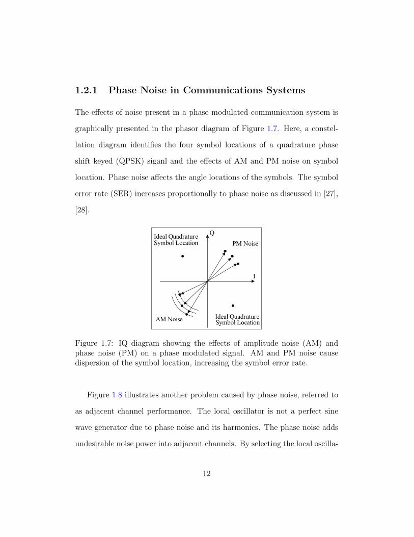
graphically presented in the phasor diagram of Figure 1.7. Here, a constel-
lation diagram identifies the four symbol locations of a quadrature phase
shift keyed (QPSK) siganl and the effects of AM and PM noise on symbol
location. Phase noise affects the angle locations of the symbols. The symbol
error rate (SER) increases proportionally to phase noise as discussed in [27],
[28].
I
QPM Noise
AM Noise Ideal QuadratureSymbol Location
Ideal QuadratureSymbol Location
Figure 1.7: IQ diagram showing the effects of amplitude noise (AM) andphase noise (PM) on a phase modulated signal. AM and PM noise causedispersion of the symbol location, increasing the symbol error rate.
Figure 1.8 illustrates another problem caused by phase noise, referred to
as adjacent channel performance. The local oscillator is not a perfect sine
wave generator due to phase noise and its harmonics. The phase noise adds
undesirable noise power into adjacent channels. By selecting the local oscilla-
12

tor and carefully analyzing its phase noise it is possible to control the degree
of interference introduced into the wanted channel [29]. For example, W-
CDMA(Wideband Code Division Multiple Access) communication network
transmits on 3.84 MHz-wide radio channels with 5 MHz apart. Therefore,
the system requires that the total power level within 3.84 MHz bandwidth at
±5 MHz and ±10 MHz offset from carrier be at -45 dBc and -50 dBc respec-
tively.
Wanted Signal Actual SignalWanted Signal Actual Signal
AdjacentChannel
AdjacentChannel
AlternateChannel
AlternateChannelChannel
PowerChannel
PowerChannel
PowerChannel
Power
Figure 1.8: Adjacent channel interference caused by local oscillator phasenoise.
1.2.2 Phase Noise in Radar Systems
Another application where phase noise determines system performance is
radar. For example, Doppler radar determines the velocity of an object by
13

multiplying the transmitted carrier with the wave reflected from the moving
target and monitoring the small change in frequency beat, shown graphically
in Figure 1.9. The scattered signal is attenuated as 1/R4 and shifted in
frequency according to:
fD =2vf0
c0
(1.13)
where fD is Doppler shift, v is speed of moving object, fo is carrier frequency
and co is speed of light. The Doppler shift for carrier frequency of 1 GHz
and objects at speeds between 10 m/s and 343 m/s is in the range of 67 Hz
and 2287 Hz. Therefore, for most Doppler shifts, the target return could be
hidden in the phase noise of the carrier.
For slower moving objects, the reflected signal is at smaller offset from the
transmitted signal. Since the phase noise of the oscillator is higher at those
frequency offsets, the probability of detection could be challenging. Another
issue in radar is the echo from ground, referred as “clutter”. The ratio of
main-beam clutter to desired target signal may be as high as 80 dB, making
it harder to separate the desired signal from the clutter.
In conclusion, specifications for phase noise of radar system components
such as local oscillators and power amplifiers, are essential and very impor-
tant [30].
1.3 Thesis Outline
The reminder of this thesis is organized as follows:
14

fo
v
f ± f
fD
fo ± fDStationary Object
Transmitter SignalTransmitter Signal
ClutterDown-converted Clutter Noise
Doppler Signal
fo fo ± fDfD
pp g
Figure 1.9: A simplified Doppler shift radar system demonstrating the effectsof phase noise on the downconverted Doppler shift. The reflected signal willbe extremely low power and can be buried under unwanted signal, clutter,or phase noise due to either the transmitter power amplifier or the receiverlocal oscillator.
• Chapter 1 presents fundamentals of phase noise and the overview of the
thesis. The theoretical basis of phase noise is presented in mathematical
form. Effects of phase noise is explained in summary.
• Chapter 2 address different types of phase noise measurements which
are used to quantify the short-term stability of an oscillator, or alter-
nately, the added noise by a 2-port component. Throughout this thesis,
phase noise measurement systems are designed, created and optimized
15
based on phase detector and frequency discriminator method. The rest
of the chapter is devoted to a more detailed description.
• Chapter 3 chapter presents an experimental method for determining
additive phase noise of individual stable transistors. In order to stan-
dardize the measurement, packaged devices are measured when con-
nected to 50 Ω input/output lines. Thus, there is no matching for low
small-signal noise figure at the input. The measured single-sideband
phase noise is used to determine the large-signal noise figure of the
packaged device. Such characterization is used as input for the design
of oscillators and power amplifiers.
• Chapter 4 presents a design method for voltage controlled oscillators
(VCOs) with simultaneous small size, low phase noise, DC power con-
sumption and thermal drift. For transistor based oscillator, the de-
sign steps which are required for a prediction of VCO phase noise and
power consumption behavior are: (1) measured resonator frequency
dependent parameters; (2) transistor additive phase noise (noise fig-
ure characterization); (3) accurate tuning element model; and (4) bias-
dependent model in case of an active load. As an illustration, the design
of a 3.4 GHz bipolar transistor VCO with varactor tuning is presented.
Oscillator measurements demonstrate low phase noise (-40 dBc@100 Hz
and better than -100 dBc@10 kHz) with an output power of 5 mW and
with a circuit footprint smaller than 0.6 cm2. The temperature stability
16
is found to be better than ±10 ppm/C from −40 C to +30 C. The
oscillators are implemented using low cost off-the-shelf surface-mount
components, including a micro-coaxial resonator. The VCO directly
modulates the current of a laser diode and this has a nonlinear load.
A short-term stability of 2 · 10−10/√τ when locked to a miniature Ru-
bidium atomic clock is demonstrated.
• Chapter 5 presents linearity in power amplifiers and its relations to
phase noise. Extensive load/source pull measurements were performed
at 900 MHz. Power amplifiers are designed using 12V HBT from Triquint
Semiconductors.
• Chapter 6 is a discussion of the main contributions of the thesis, as
well as some suggestions for future work.
17

Chapter 2
Phase Noise Measurement
Techniques
2.1 Introduction to Phase Noise Measurements
The purpose of a phase noise measurement is to quantify the short-term sta-
bility of an oscillator, or alternately, the added noise by a 2-port component.
There are several methods used to measure phase noise [12]:
(1) Spectrum analyzer measurement involves directly measuring the power
spectral density of device in terms L(fm) using spectrum analyzer.
This measurement can be performed as long as analyzer’s phase noise
is better than the one from the measured device. This is the simplest
and easiest method.
(2) The ’time domain technique’ or heterodyne frequency counter. The

device under test and the reference are downconverted with mixer to a
low IF frequency or beat frequency. Then a high resolution frequency
counter is used to periodicly measure this signal frequency. The time
domain technique is a very sensitive measurement method for measur-
ing close-in phase noise (less than 100 Hz offset from the carrier in the
frequency domain). However, it surpasses it limits for noise measure-
ments at offsets from the carrier larger than 10 kHz [11].
(3) The phase detector method measures voltage fluctuations directly pro-
portional to the combined phase fluctuations of the two input sources.
This method has the lowest noise floor and therefore has the best phase
noise detection capability [31].
(4) The frequency discriminator method, unlike the phase detector method,
measures the phase noise of a single oscillator without using another
source for downconversion. This method converts frequency fluctua-
tions of a source into voltage fluctuations [32].
Throughout this thesis, phase noise measurement systems are designed,
created and optimized based on methods (3) and (4) and the rest of
the chapter is devoted to a more detailed description.
19

2.2 Phase Detector Method
The phase detector technique is also referred to as the two-source or the
quadrature technique, Figure 2.1. It is used to measure high quality stan-
dards with good close in noise(150 dBc/Hz at 10 Hz offset for frequencies
around 1 GHz) or free running oscillators with low broadband noise. In this
f
DUT
Δφ→ ΔV Low NoiseAmplifier
FFT
fo
DUT
Low
FFT Analyzer90°
fo
Reference
LowPass Filter
fo
Phase LockLoop
Figure 2.1: Phase Detector Method. Small fluctuations from nominal volt-ages are equivalent to phase variations. The phase lock loop keeps two signalsin quadrature, which cancels carriers and converts phase noise to fluctuatingDC voltage.
method, a double-balanced mixer is used as a phase detector. Two sources,
at the same frequency and 90 out of phase(in quadrature), are input to the
mixer. The mixer sum 2fo is filtered off with a low pass filter, and the output
is a DC voltage with an average output of 0 V. The DC voltage fluctuations
are directly proportional to the combined phase noise of the two sources.
The noise signal is amplified using a low noise amplifier (LNA)and measured
using a spectrum analyzer.
20

The mixer selection is very important to the overall system performance.
The noise floor sensitivity is related to the mixer input levels, therefore higher
power level mixers yield better performance. However, one has to be care-
ful to match mixer drive to available source power. More detailed mixer
operation as a phase detector is explained in the next section.
In an actual system, the sources need to be maintained in phase quadra-
ture. A phase lock loop (PLL) is used in a feedback path to one of the
oscillators. The error voltage out of the PLL is applied to an electronically
tunable source forcing it to track the other in phase.
The most critical component of the phase detector method is the reference
source. As explained earlier, a spectrum analyzer measures the sum of noise
from both sources. Therefore, the reference source must have lower phase
noise than device under test, DUT. Usually 10 dB margin is sufficient enough
to ensure correct measurements [12]. If a reference source with low enough
phase noise is not available one can use source comparable to the device
under test. Then each source contributes equally to the total noise and 3 dB
is subtracted from the measured value [31].
In the summary, the phase detector method has excellent system sensi-
tivity, but on the other hand its complexity (PLL and two oscillators are
required) might cause additional problems.
21

2.2.1 Mixers as Phase Detectors
Figure 2.2 shows typical VIF varying as the cosine of the phase difference ∆φ
between LO and RF signals. The response of VIF is fairly linear in the region
∆φ = φLO−φRF = π/2 + δφ. This is also the region where the sensitivity of
the phase detector (dVIF/dφ) is maximum [33].
1
0.60.8
1
Region of Operation
δφ
0.20.4
V)
Region of Operation
0 4-0.2
0
VIF
(V
∆VIFV IF
-0 8-0.6-0.4
0 20 40 60 80 100 120 140 160 180-10.8
φLO - φRF (degrees)φLO-φRF (degrees)LO RFφLO φRF (degrees)
Figure 2.2: Typical phase detector response curve varies as cos(∆φ+π). Thedetector response is fairly linear over ∆φ = π/2 + δφ.
Assume that the phase detector output is described by
VIF (t) = ±V cos[(ωR − ωL)t+ ∆φ(t) + π] (2.1)
where V is the peak amplitude of the voltage seen at ∆φ = 0 or π. As
mentioned before mixer’s two input signals are at the same frequency, ωR =
ωL and 90o out of phase. Substituting these values in Equation 2.1 we get
∆VIF (t) = ±V sin(δφ(t)) (2.2)
22

where ∆VIF (t) is instantaneous voltage fluctuations around DC and δφ(t)
is instantaneous phase fluctuations. For δφ(t) 1rad, sin(δφ(t)) ' δφ(t)
which indicates that within linear response region, phase detector sensitivity
varies linearly with maximum output voltage [34],[35]:
∆VIF = V δφ = Kφδφ (2.3)
where Kφ is phase detector constant (volts/radian), which is equal to the
slope of the mixer sine wave output at the zero crossings.
2.3 The Frequency Discriminator Method
In the frequency discriminator method, the frequency fluctuations of the
source are translated to low frequency voltage fluctuations which can then
be measured by a baseband analyzer. There are several common implemen-
tations of frequency discriminators including cavity resonators, RF bridges
and a delay line [36].
The delay-line measurement system is chosen for the flexibility in mea-
suring a free-running oscillator between 1 GHz and 10 GHz. The delay-line
technique has sufficient sensitivity to measure most microwave oscillators
with loaded Q-factors of several hundred and does not require a second ref-
erence oscillator [37].
23

2.3.1 Operation and Calibration
Delay line discriminator measurements for oscillators were first introduced
in 1966 by Tykulsky[38] and improved by Halford in 1975[39] with a cross-
correlation system. The delay-line system developed in this work is shown in
Figure 2.3. In this measurement, the oscillator output is split using a 3 dB
splitter, one of the outputs is delayed, and multiplied in a mixer with the
non-delayed path. The mixer operates as a phase-detector, translating phase
changes between the RF and LO ports to a measurable voltage at the IF.
The measured voltage spectral density is proportional to the phase noise of
the oscillator.
LO LNA
Phase Shifter
Amp
Δf→Δφ→ ΔV
LO
RF
LNAFFT
Amp
Delay Liney
Figure 2.3: Delay-line phase noise measurement system schematic. The os-cillator under test is amplified to 18 dBm and split with a 3 dB power divider.One branch is delayed by 125 ns and phase compared against reference branchusing a double balanced mixer as a phase detector. The mechanical phaseshifter is used to set the system in quadrature (Mixer IF = 0 V). A LNAamplifies the mixer output voltage before sampling with an FFT analyzer.
Delay-line discriminators are limited by the loss of the delay-line due
to the power requirements for the mixer. Using lower power than required
will lead to degraded performance of the system. The delay line used in
24
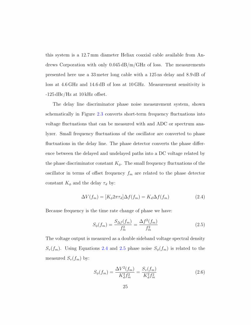
this system is a 12.7 mm diameter Heliax coaxial cable available from An-
drews Corporation with only 0.045 dB/m/GHz of loss. The measurements
presented here use a 33 meter long cable with a 125 ns delay and 8.9 dB of
loss at 4.6 GHz and 14.6 dB of loss at 10 GHz. Measurement sensitivity is
-125 dBc/Hz at 10 kHz offset.
The delay line discriminator phase noise measurement system, shown
schematically in Figure 2.3 converts short-term frequency fluctuations into
voltage fluctuations that can be measured with and ADC or spectrum ana-
lyzer. Small frequency fluctuations of the oscillator are converted to phase
fluctuations in the delay line. The phase detector converts the phase differ-
ence between the delayed and undelayed paths into a DC voltage related by
the phase discriminator constant Kφ. The small frequency fluctuations of the
oscillator in terms of offset frequency fm are related to the phase detector
constant Kφ and the delay τd by:
∆V (fm) = [Kφ2πτd ]∆f(fm) = Kd∆f(fm) (2.4)
Because frequency is the time rate change of phase we have:
Sφ(fm) =S∆f (fm)
f 2m
=∆f 2(fm)
f 2m
(2.5)
The voltage output is measured as a double sideband voltage spectral density
Sv(fm). Using Equations 2.4 and 2.5 phase noise Sφ(fm) is related to the
measured Sv(fm) by:
Sφ(fm) =∆V 2(fm)
K2df
2m
=Sv(fm)
K2df
2m
(2.6)
25

Conversion to single sideband phase noise gives:
Lφ(fm) =Sv(fm)
2K2df
2m
(2.7)
or, in dB:
Lφ(fm)[dBc/Hz] = Sv(fm)− 3− 20log(Kd)− 20log(fm) (2.8)
With a single calibration of the mixer as a phase detector, Kφ and known
delay τd, the phase noise of an oscillator can be measured on an FFT analyzer.
Kφ is in V/rad and is determined by measuring the DC output voltage change
of a mixer while in quadrature (nominally 0 V DC) for a known phase change
in one branch of discriminator. The value of Kd is dependent upon the RF
input power of the mixer,which in turn is directly proportional to the noise
floor shown in Figure 2.4.
Using Z-parameters the sensitivity of the delay line discriminator can
be determined first by introducing the Q-factor defined with respect to the
phase of the open-loop transfer function φ(ω) at the resonance of parallel
RLC circuit:
φ(jω) = tan−1 Imag(Z(jω))
Real(Z(jω))(2.9)
and
Q =1
R
√L
C=ω
2
δφ
δω(2.10)
A coaxial delay-line has a linear phase relation with frequency across the
usable bandwidth of the transmission line. Relating this linear phase rela-
tionship in a coaxial line to the derivative of the phase change in a resonator
26

-15 -10 -5 0 5 10 15-185
-180
-175
-170
-165
-160
-155
-150
-145
Mixer RF Port Level (dBm)
App
roxi
mat
e N
oise
Flo
or L
evel
(dB
c/H
z)
Figure 2.4: The ideal phase detector sensitivity in terms of RF power (as-suming LO power is great than RF) and phase detector constant Kφ. Thenoise floor sensitivity is 1:1 to mixer power input.
results in an effective Q, QE for a transmission line with time delay τd:
QE = πf0τd (2.11)
The effective Q-factor increases linearly with both delay line length and
frequency of operation. Using QE as the Q-factor in the Leesons equation
and using an approximate mixer noise floor of -170 dBc. The flicker corner
is set at 10 kHz, typical for a silicon diode mixer. The measurement phase
noise floor is calculated by:
Lφ(fm) = 10log
[(1 +
1
(2πτdfm)2
)(1 +
fc
fm
)]+Nmixerfloor (2.12)
The digitization of the mixer output voltage is completed by a Stanford
Research Systems SR760 FFT Analyzer which requires the addition of an
27

LNA due to the insufficient sensitivity of the analyzer. An op-amp from
Analog Devices, part AD797, in a non-inverting configuration and gain of
40 dB is used as a pre-amplifier, shown in Figure 2.3. The input voltage noise
is 1 nV/Hz with a flicker corner of 100 Hz. The non-inverting input is a 2 kΩ
resistor to ground. Several values were tested for phase detector optimization
[35]. Above 2 kΩ, the phase detector sensitivity does not improve but the
input offset current of the AD797 produced a significant voltage output offset.
Below 500 Ω, the phase detector sensitivity was reduced by up to a few dB.
This chapter presented an overview of various phase noise measurement
techniques, focusing on the discriminator method. In Chapter 3, details
of implementation of the measurement system are presented. This type of
measurement is used for characterizing stable transistors in large-signal op-
erations with the main contributions reported in [40], as well as low phase
noise oscillators described in [3].
28

Chapter 3
Transistor Phase Noise
Characterization
This chapter presents an experimental method for determining additive phase
noise of individual stable transistors. In order to standardize the measure-
ment, packaged devices are measured when connected to 50 Ω input/output
lines. Thus, there is no matching for low small-signal noise figure at the
input. The measured single-sideband phase noise is used to determine the
large-signal noise figure of the packaged device. Such characterization is used
as input for the design of oscillators and power amplifiers.

3.1 Introduction
Transistors are very important components used in any power amplifier or
oscillator design and their characteristics highly influence the final design
performance. There are few terms that are used throught the thesis which
need to be defined.
Linearity is the ability of an amplifier to deliver output power in exact
proportion (the gain) to the input power. Non-linear response appears in an
amplifier when the outputs are driven to a point near saturation. As this
level is approached, the amplifier gain falls off, or compresses. The tracking
relationship between output and input levels is a direct function of the gain.
When the gain compresses, the amplifier’s linearity is lost [41],[42].
Also, most of the transistor parameters, such as S-parameters or Noise
Figure, are measured in small signal environment which correlates to low
power levels, long before the saturation point. On the other hand, when
used in amplifier or oscillator design, transistors operate under large signal
conditions. Since this is nonlinear region, those parameters could significantly
change compared to small signal measurements. If one uses these small signal
parameters in the design, it could lead to inaccurate and unwanted final
performance.
The noise figure (NF ) is a common parameter given in transistor specifi-
cation sheets and is the focus of this chapter. In practice, the NF is measured
in the absence of a carrier signal by injection of band-limited small-signal
30
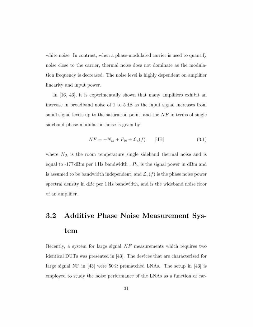
white noise. In contrast, when a phase-modulated carrier is used to quantify
noise close to the carrier, thermal noise does not dominate as the modula-
tion frequency is decreased. The noise level is highly dependent on amplifier
linearity and input power.
In [16, 43], it is experimentally shown that many amplifiers exhibit an
increase in broadband noise of 1 to 5 dB as the input signal increases from
small signal levels up to the saturation point, and the NF in terms of single
sideband phase-modulation noise is given by
NF = −Nth + Pin + La(f) [dB] (3.1)
where Nth is the room temperature single sideband thermal noise and is
equal to -177 dBm per 1 Hz bandwidth , Pin is the signal power in dBm and
is assumed to be bandwidth independent, and La(f) is the phase noise power
spectral density in dBc per 1 Hz bandwidth, and is the wideband noise floor
of an amplifier.
3.2 Additive Phase Noise Measurement Sys-
tem
Recently, a system for large signal NF measurements which requires two
identical DUTs was presented in [43]. The devices that are characterized for
large signal NF in [43] were 50 Ω prematched LNAs. The setup in [43] is
employed to study the noise performance of the LNAs as a function of car-
31
rier power level. Measuring residual PM white noise, the degradation of the
amplifier NF with input power is observed. It is shown that LNA’s NF can
increase dramatically with gain compression. Garmendia and Portilla con-
clude that the growth of NF in nonlinear operating conditions is explained
due to the gain compression itself and the increasing level of the noise added
by the amplifier.
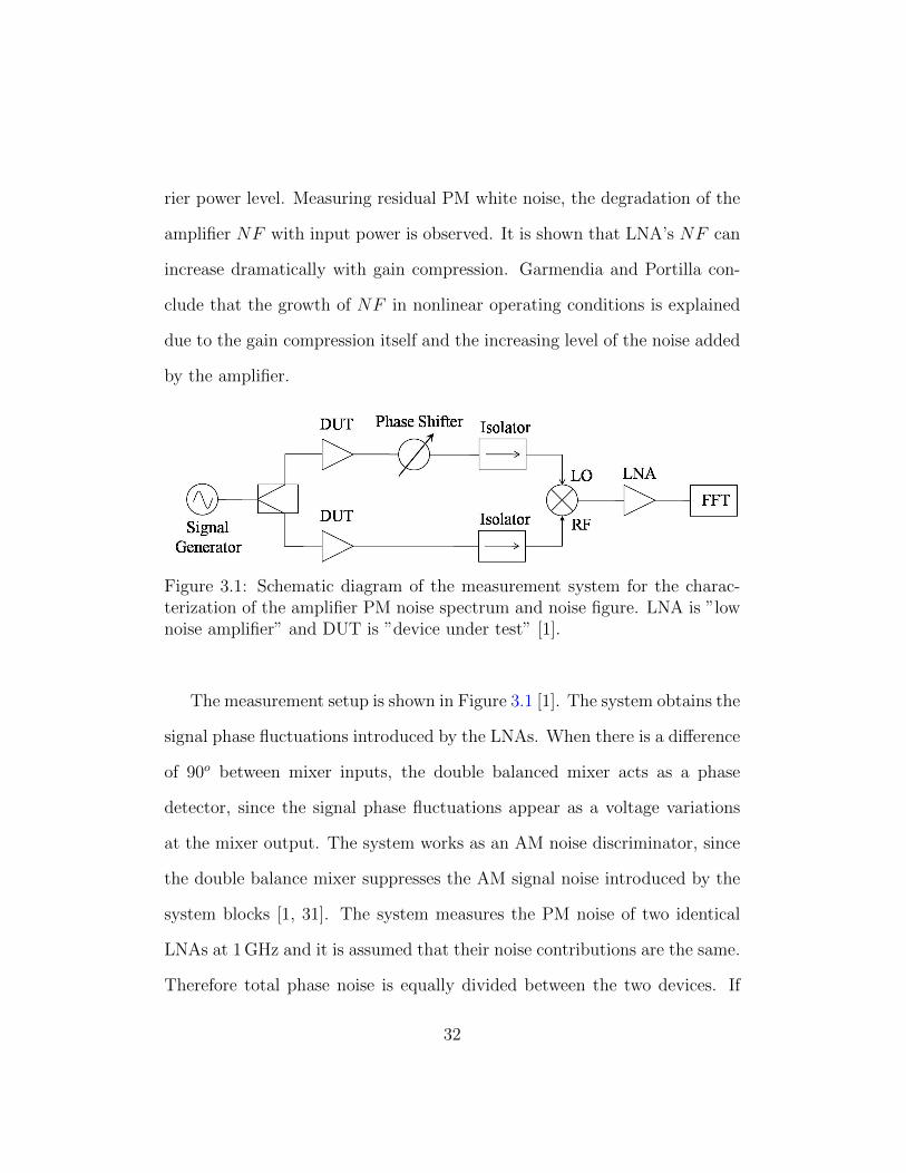
Figure 3.1: Schematic diagram of the measurement system for the charac-terization of the amplifier PM noise spectrum and noise figure. LNA is ”lownoise amplifier” and DUT is ”device under test” [1].
The measurement setup is shown in Figure 3.1 [1]. The system obtains the
signal phase fluctuations introduced by the LNAs. When there is a difference
of 90o between mixer inputs, the double balanced mixer acts as a phase
detector, since the signal phase fluctuations appear as a voltage variations
at the mixer output. The system works as an AM noise discriminator, since
the double balance mixer suppresses the AM signal noise introduced by the
system blocks [1, 31]. The system measures the PM noise of two identical
LNAs at 1 GHz and it is assumed that their noise contributions are the same.
Therefore total phase noise is equally divided between the two devices. If
32

the devices are not close to identical, and their contributions are different
and unknown, it could lead to inaccurate results with an error in NF up to
3 dB. In [43], Garmendia and Portilla examined two different types of LNAs
with small signal gains of 32 and 27.2 dB and linear NF of 1.2 and 2 dB.
They measured NF with input power drive up to 2 dB gain compression.
The first LNA NF increased from 1.2 to 4.6 dB (3.4 dB increase), while the
second LNA NF experienced much higher increase from 2 to 11.4 dB (9.4 dB
increase).
LO LNA
PHASE SHIFTER
Amp 3
RFFFT
3.5 GHzSource
DUT
Amp 1
NLTL 2100 MHz 500 MHz 3 5 GHz
Amp 2
NLTL 1
3.5 GHzSource OutputNLTL-2100 MHz
Crystal Oscillator
500 MHzBPF
3.5 GHzBPF
NLTL-1
(a)
LO LNA
PHASE SHIFTER
Amp 3
RFFFT
3.5 GHzSource
DUT
Amp 1
NLTL 2100 MHz 500 MHz 3 5 GHz
Amp 2
NLTL 1
3.5 GHzSource OutputNLTL-2100 MHz
Crystal Oscillator
500 MHzBPF
3.5 GHzBPF
NLTL-1
(b)
Figure 3.2: (a) The block diagram of the additive phase noise measurementsystem. (b) Details of 3.5 GHz source
In the measurement system presented in this chapter and shown in Figure
33

3.2, both prematched and unmatched devices can be characterized, and there
is no need for two identical devices under test (DUTs). The noise due to the
oscillator are correlated and canceled at the phase detector. Noise due to
the amplifier is uncorrelated and measured as additive phase noise. In this
work the carrier frequency is chosen at 3.5 GHz, but we show it is scalable.
This is significantly higher in frequency than previous setup. Going to higher
frequency presents challenge in finding a good signal generator with very low
phase noise.
The additive phase noise system is composed of a 3.5 GHz source which is
explained in next section, power splitter, a phase shifter, and a mixer (Figure
3.2). The phase shifter establishes true phase quadrature between the two
signals at the mixer inputs. The output of the mixer after amplification is
measured by Stanford Research Systems SR760 FFT spectrum analyzer. The
measured RMS voltage spectral density corresponds to the additive phase
noise of the DUT, a transistor in our case. The system with the 3.5 GHz
source provides a noise floor of -168 dBc/Hz at 100 kHz offset from the carrier
(Figure 3.3), which is much lower than the phase noise of the transistors under
test. System noise floor needs to be lower than transistor’s additive phase
noise in order to detect and measure correct data.
The single sideband phase noise is proportional to the measured voltage
spectral density at the output of the mixer by the relation:
Lφ = Sv(fm)− 20log(Kd)− 3 [dBc/Hz] (3.2)
34
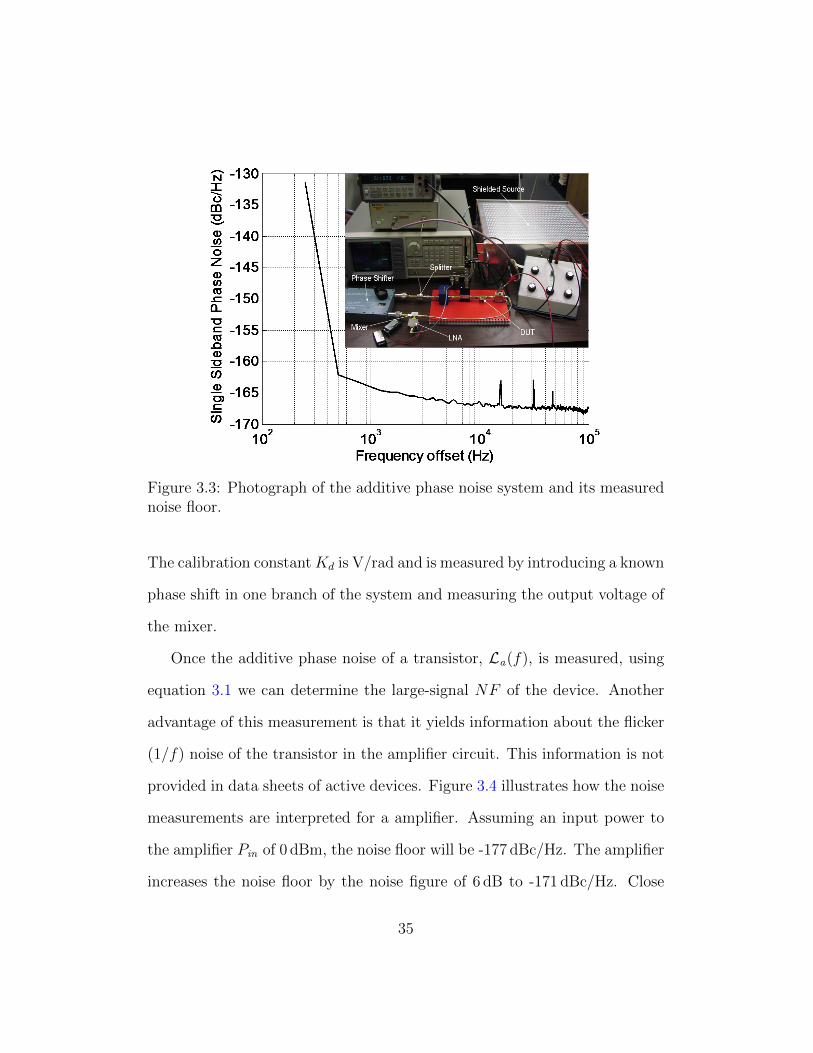
Figure 3.3: Photograph of the additive phase noise system and its measurednoise floor.
The calibration constantKd is V/rad and is measured by introducing a known
phase shift in one branch of the system and measuring the output voltage of
the mixer.
Once the additive phase noise of a transistor, La(f), is measured, using
equation 3.1 we can determine the large-signal NF of the device. Another
advantage of this measurement is that it yields information about the flicker
(1/f) noise of the transistor in the amplifier circuit. This information is not
provided in data sheets of active devices. Figure 3.4 illustrates how the noise
measurements are interpreted for a amplifier. Assuming an input power to
the amplifier Pin of 0 dBm, the noise floor will be -177 dBc/Hz. The amplifier
increases the noise floor by the noise figure of 6 dB to -171 dBc/Hz. Close
35

to the carrier, the flicker noise of the amplifier increases the phase noise at
10 dB/decade with corner frequency fc = 1 kHz.
-140
-145Lf (fm) = 10log10(1+ fc/fm) -177dBc
-155
-150
f = 1kHz
165
-160fc = 1kHz
kTF/2 =-177dBc + 6dB = -171dBc
-170
-16510dB/decade
180
-175 kT/2Pin = -177dBc NF = 6dB
101
102
103
104
105-180
Figure 3.4: Interpretation of noise measurements; e.g. assuming an inputpower to the amplifier Pin of 0 dBm, the noise floor will be -177 dBc/Hz. Theamplifier increases the noise floor by the noise figure of 6 dB to -171 dBc/Hz.Close to the carrier, the flicker noise of the amplifier increases the phase noiseat 10 dB/decade with corner frequency fc = 1 kHz.
3.3 3.5GHz Source
To ensure that the noise contribution of the measurement system is sig-
nificantly lower than the phase noise of the transistor under test, a very
clean source at the carrier frequency is required. A 100 MHz temperature-
controlled crystal oscillator (Wenzel 501-04516D) is chosen as the fundamen-
36

tal source. Because of their high Q factors, lower frequency crystal oscilla-
tors multiplied several times (35 in this case) typically exhibit better phase
noise than available fundamental-frequency oscillators at S-band, illustrated
in Figure 3.5.
z) Mi ti 3 5GH
(dB
c/H
z
Spectrum Microwave 3 5GH O ill t
Micronetics 3.5GHz Oscillator
M3500-2250
e N
oise
3.5GHz OscillatorHV83T
Crystek Microwave 3.5GHz Oscillator
and
Phas CVCO55BH
e Si
deba
Sing
le
Frequency Offset (Hz)
Figure 3.5: Custom 3.5GHz source phase noise is better than currently com-mercially available oscillators
The 100 MHz output signal is amplified through a low noise amplifier
(Hittite HMC479MP86) to a 50 mW level into a 50 Ω load. The output of the
amplifier is connected directly to a nonlinear transmission line (NLTL) which
operates as a low phase noise comb generator or frequency multiplier and is
described in more details later. There are two NLTLs used in the design. The
first nonlinear transmission line, NLTL-1, generates significant harmonics
up to 1 GHz, and the 500 MHz signal is filtered out. It is amplified using
37

two cascaded amplifiers (Hittite HMC482ST89) with a total of 30 dB gain
and an output power of 50 mW. The amplified 500 MHz signal is multiplied
by a subsequent NLTL-2 which generates the required 3.5 GHz harmonic at
around -15 dBm power level. The other generated harmonics are suppressed
by at least 30 dB through a 3.5 GHz band-pass filter. The signal is amplified
using a 35 dB gain HP 8449B preamplifier and is used as a 3.5 GHz source
for the additive phase noise measurement system shown in Figure 3.2.
3.4 Nonlinear Transmission Line Multipliers
The unique part of the measurement setup is the source, which includes two
NLTLs. In [44] it is shown that appropriately biased NLTLs have excellent
phase noise performance as frequency multipliers, approaching the theoretical
limit of
L(Nf) = 20logN + L(f) (3.3)
where N is the fundamental frequency multiplication factor. L(Nf) in
dBc/Hz is the phase noise at the Nth harmonic frequency and L(f) in dBc/Hz
is the phase noise at the fundamental at the same offset. The NLTLs from
Figure 3.2 are periodic artificial lumped-element transmission lines, as shown
in Figure 3.6. Typically, a varactor is used as a voltage-variable capacitor,
resulting in a voltage dependent phase velocity. With large signal input
voltage, the voltage variation of the NLTL capacitance results in nonlin-
ear wave propagation and harmonics of the input frequency are generated
38

L L L LL L L L
C(V) C(V) C(V) C(V)L C(V) C(V) C(V) C(V)Lbias
(a)
20 2.0
-20
-10
0
10
RFo
ut)
0.5
1.0
1.5
out),
V
-50
-40
-30
-60
dBm
(
-0.5
0.0
1 0
ts(R
F
0.1 0.2 0.3 0.4 0.5 0.6 0.7 0.8 0.90.0 1.0
-60
freq, GHz
2 4 6 8 10 12 14 16 180 20-1.0
time, nsec
(b)
Figure 3.6: (a) Simplified NLTL schematic showing the distributed L-C el-ements. (b) Simulated spectrum of the 8-section NLTL-1 and time domainoutput voltage waveform using Agilent ADS Harmonic Balance. The diodesare reverse-biased. The multiplication efficiency for NLTLs is low: for 17 dBmof 100 MHz input, the 500 MHz output of NLTL-1 is approximately -11 dBm.The pulse compression in the NLTL occurs due to the voltage dependentphase velocity. The flat line at the bottom of the time domain outputs iswhere the NLTL is in hard forward conduction. Diode model is SMV1247-079
[45, 46, 47, 48, 49]. The inductors in the 8-stage NLTL-1 are all equal with
L1 = 10 nH and the variable capacitors are hyper-abrupt varactor diodes
with zero bias capacitance of 9 pF and the lowest capacitance of 0.6 pF at
higher voltages. The characteristic impedance of the line is around 50 Ω for
the mid-bias point. NLTL-2 is implemented similarly as an 8-section line
39

with L2 = 4 nH and a different diode with a capacitance range from 2 pF
(zero bias) to 0.5 pF. The diodes are reverse-biased. The multiplication effi-
ciency for NLTLs is low: for 17 dBm of 100 MHz input, the 500 MHz output
of NLTL-1 is approximately -11 dBm, Figure 3.6.
Alternative multipliers using, e.g. step recovery diodes (SRD), have been
shown to have an inferior phase noise [23]. The NLTLs demonstrate near
20logN multiplication behavior, while the SRDs is measured to have a 40 dB
increase for N = 10 multiplication, or a 40logN relationship [50].
3.5 Measurement Results
To demonstrate the method described above, the additive phase noise at
3.5GHz was measured for three different BJT transistors: (1) Infineon BFP405;
(2) Infineon BFP420; and (3) NE894M13 from California Eastern Labs (CEL).
The transistors are inserted in a 50Ω environment without any matching cir-
cuits at input or output, and with emitters grounded and base bias resistors
of 20 kΩ, as in Figure 3.7.
Figure 3.8 shows the measured system noise floor and additive phase noise
for all three transistors at Vbias = 2.5 V and Pin = −10 dBm. The last data
point, at 100 kHz offset, is considered the thermal noise level and the NF of
the transistor is calculated from Eq. 3.1 [51].
Figure 3.9 illustrates the large-signal noise figure of the transistors and
its dependence on the input power up to around 4 dB gain compression.
40

Vbias
20kΩ Bias Tee
50Ω
50ΩPin
Pout
RF Choke
DC Bl k
RF Choke
Bias Tee
DUT 50Ωin DC Block
DC Block
Figure 3.7: Unmatched testing circuit enviroment used for transistor additivephase noise measurements
The transistors are at Vbias = 2 V. There is an increase in NF compared to
the small signal value given in the data sheets. This effect is due to the
nonlinearity in the transistor manifested as AM to PM conversion.
Figure 3.10 illustrates the large signal NF measurements at different bias
points. The input power level presented to the transistors is around -11 dBm
for BFP405 and around -8 dBm for BFP420 and NE894M13. At these power
levels the transistors are at 3 dB saturation points. As expected, the NF
decreases as the voltage is increased.
The plots in Figures 3.8-3.10 are chosen to illustrate the importance of
characterization at different power levels and bias points. For example, Fig-
ure 3.8 indicates that the BFP405 device (blue line in figure) seems to have
the largest phase noise, but if DC power consumption is an important pa-
41

Figure 3.8: Additive phase noise measurements of each transistor at Vbias =2.5V and Pin = −10 dBm. Existing spikes in the plot are due to the monitorrefresh rate of the FFT analyzer.
rameter, Figure 3.10 indicates that the BFP405 device is the optimal choice
for oscillator design since it has the lowest large signal noise figure for low
DC power levels. In conclusion, table 3.1 shows comparison between NF
from a PM noise measurement and the conventional small-signal NF given
in data sheets.
Table 3.1: Data sheet noise parameters compared to measured data
Device Small Signal Zopt for Small Signal Large SignalType NF @ Zopt NF NF @ 50 Ω NF @ 50 Ω
BFP 405 1.46 dB 60.94+j38.38 1.8 dB 7.1 dBBFP 420 1.38 dB 32-j1.29 1.48 dB 8 dB
NE894M13 2 dB 29.090-j5.3 N/A 8.5 dB
42

Figure 3.9: Large signal NF measurements with different input power, fre-quency, bias. The small-signal noise figures from the specification sheetsare 1.25, 1.1 and 1.4 dB for the BPF405, BFP420 and NE894M13 devices,respectively
3.6 Summary
In this chapter, a measurement system for characterizing additive phase noise
of stable transistors under different bias and input power is presented. It is
observed that the NF from a PM noise measurement is higher than the con-
ventional small-signal NF given in data sheets obtained from thermal noise
measurements. It is also shown that NF changes with input power and DC
power consumption. Another advantage of this measurement is that it yields
information about flicker (1/f) noise of a transistor. Although the measure-
ments presented here are done at 3.5 GHz, this approach can be easily applied
43

Figure 3.10: Large signal NF measurements at different bias points and con-stant input power of -8 dBm.
to any frequency with appropriate modifications. For example, an X-band
version would require filtering of higher harmonics in first stage(e.g 1 GHz)
and than multiplying it through redesigned NLTL to desired frequency. An-
other approach would be starting with a higher frequency source with ade-
quate phase noise characteristics. Higher frequency crystals in the GHz range
are moving from research phase and becoming commercially more available
[52],[53], [54]. Finally, the most important conclusion of this chapter is that
additive phase noise measurements give a more useful characterization of a
transistor noise performance for oscillators and PAs than small signal NF
which is commonly supplied by manufacturers for LNA design.
44

Chapter 4
Design Method for Low-Power,
Low-Phase Noise Voltage
Controlled Oscillators
This chapter presents a design method for voltage controlled oscillators (VCOs)
with simultaneous small size, low phase noise, DC power consumption and
thermal drift. For transistor based oscillator, the design steps which are re-
quired for a prediction of VCO phase noise and power consumption behavior
are: (1) measured resonator frequency dependent parameters; (2) transistor
additive phase noise (noise figure characterization); (3) accurate tuning el-
ement model; and (4) bias-dependent model in case of an active load. As
an illustration, the design of a 3.4 GHz bipolar transistor VCO with varactor
tuning is presented. Oscillator measurements demonstrate low phase noise

(-40 dBc@100 Hz and better than -100 dBc@10 kHz) with an output power of
5 mW and with a circuit footprint smaller than 0.6 cm2. The temperature
stability is found to be better than ±10 ppm/C from −40 C to +30 C.
The oscillators are implemented using low cost off-the-shelf surface-mount
components, including a micro-coaxial resonator. The VCO directly modu-
lates the current of a laser diode and this has a nonlinear load. A short-term
stability of 2 · 10−10/√τ when locked to a miniature Rubidium atomic clock
is demonstrated.
4.1 Application
There are a number of microwave applications that require low-phase noise
oscillators. An example of a set of challenging requirements is the case
of a chip-scale atomic clock (CSAC) which contains a microwave voltage-
controlled oscillator (VCO) which locks to the atomic resonance of alkali
atoms, such as Rubidium, Figure 4.1. When the entire miniature atomic
clock needs to be in a 1 cm3, 30 mW package [55], a large fraction of the
power is dedicated to thermal management [56] and locking [57], leaving a
small power budget for the VCO. To be comparable in stability with existing
compact atomic frequency references, fractional frequency instability below
10−11 is required at one-hour integration times and longer [56].
The requirements for this new technology are pushing the state-of-the art
in oscillator design to develop a local oscillator (LO) that exhibit combined
46

3.41734 GHzVCO
dbac
kFe
ed
VCSEL 87Rb DetectorVCSEL Rb DetectorN
Rb
NN
N
N
NRb
NN
Figure 4.1: Simplified schematic chip scale atomic clock. The output fromthe voltage controlled oscillator (VCO) directly modulates VCSEL (vertical-cavity surface-emitting laser) current. The photodetector output signal issent from the physics package to the locking electronics, which stabilizes theVCO and provides thermal stabilization and other control to the physics [2].
lower phase noise, less power consumption, and smaller size than previously
published voltage-controlled oscillators. To effectively modulate the laser
light field, the LO frequency must be either exactly equal to or half of the
hyperfine ground-state splitting frequency for Rubidium (or Cesium) atoms
and tunable to compensate for frequency differences due to temperature, part
tolerances, and other variables. Designing for half of the hyperfine splitting
frequency, a VCO is needed at 3.417 GHz for Rb [58].
In this chapter, we discuss the design and the experimental validation
of the design method for low-phase noise and low-power consumption VCOs
designed for a very specific and precise frequency and output power while
47

Bias
AB
Output
C D
Figure 4.2: Simplified schematic of a VCO. The transistor (B) is shown as abipolar device, and the tuning element is a diode (C). The resonator (A) isconnected to the input terminal of the transistor while the load (D) can beactive and is connected to the output terminal. The bias line is not assumedto be an ideal choke.
simultaneously satisfying tight volume constraints. We show that the method
can be applied effectively for design of VCOs that meet requirements for
challenging applications such as CSAC.
4.2 Experimentally-Based Oscillator Design
Method
When designing the VCO, and in reference to Figure 4.2, the oscillator circuit
is divided as follows: (A) resonator, including coupling to the circuit; (B)
transistor and biasing circuit; (C) tuning element and coupling to the circuit;
and (D) load and its bias-dependent properties. All four elements need to
be independently characterized for a successful prediction of final oscillator
48

design behavior.
4.2.1 Resonator Selection
Generally, when very small size, microwave frequency and high Q are of inter-
est, the choices for resonators are: quartz crystals, coaxial resonators, MEMS
mechanical resonators, and recently designed bulk acoustic resonators, Ta-
ble 4.1 [59]. In the example presented here, a λ/4 ceramic filled coaxial
resonator [51] is chosen because of its high Q, small size (2 mm by 2 mm
by 3.9 mm for 3.4 GHz) and good thermal stability (+7 ppm/C, with other
values available). Such resonators have more than three times better sta-
bility over wide temperature variations than recently produced high-Q film
bulk acoustic resonators (FBARs) [6]. Despite the relatively low cost of the
surface-mount coaxial resonators (several dollars per resonator), it remains
the most expensive component of the microwave oscillator.
Table 4.1: Available small size resonators and their attributes
Resonator Research Level Coaxial MEMS BulkType Quartz Mechanical Acoustic
Q factor > 10000 200 < 5000 250-1500Frequency < 100 MHz < 6 GHz < 3 GHz < 10 GHz
Temperature poor +7 ppm/C poor +28 ppm/CStability
The resonator is a ceramic-filled coaxial quarter-wavelength transmission
line which is modeled as a parallel RLC circuit at self-resonance, illustrated in
Figure 4.3. When used below resonance and coupled capacitively to the rest
49

of the circuit, the resonator becomes a series RLC circuit. The unloaded Q is
measured to be Q0 = 210 at self-resonance [60]. If the Q factor is sufficiently
high, the magnitude of the input impedance bandwidth gives a reasonable
estimate. With a dielectric constant of 37.4, a characteristic impedance of
9.2 Ω, and an outside diameter of 2.0 mm, the inside diameter was calculated
to be 0.787 mm for a circular coaxial transmission line model in Agilents ADS
software.
HP8510C
0.2pFλ/4
εr= 37
R50 ΩS11
Z11
Figure 4.3: Resonator schematic and plot showing the method used to mea-sure the self-resonance frequency and Q. The input impedance Z11 is calcu-lated from S11 to give a close approximation of unloaded impedance responseof the resonator, apart from 50 Ω load of network analyzer. The unloaded Qwas calculated from Z11 with the use of the magnitude and phase relation-ship.
The thermal frequency drift of the coupled resonator was measured with
a simple op-amp feedback circuit, a power resistor (heat source) and a ther-
mistor (for measurement) affixed to the brass plate. While the frequency
shift with temperature is specified by the manufacturer as +7 ± 2 ppm/C,
the overall frequency shift was found to vary from approximately −6 ppm/C
near room temperature to −13 ppm/C at higher temperatures, most likely
50

due to the thermal coefficient of the series capacitor. (a Panasonic series
ECD multilayer ceramic capacitor with a C0G temperature coefficient of
0± 30 ppm/C).
4.2.2 Transistor Noise Characterization
One of the parameters that can aid in predicting the final oscillator phase
noise is the transistor noise figure (NF ) [61],[62], which is given in most man-
ufacturers data sheets, but is measured at small signal levels. An oscillator
is stabilized by the self–limiting nature of gain compression. Therefore, in
oscillators, transistors operate in large signal mode, usually 2-3 dB in com-
pression. In [16], as it is explained in the previous chapter, one can obtain
the transistor’s NF using equation 3.1. From here, the oscillator phase noise
can be found using the following equation [16]:
L(fm) = 10log
[(F · kT2 · Pin
)·(
1 +f 2
0
(2 · fm ·Qloaded)2
)·(
1 +fc
fm
)](4.1)
where f0 is the carrier frequency, L(fm) is the ratio of the phase noise in
a 1Hz bandwidth to the common oscillator output level, fm is the carrier
frequency offset, fc is the noise edge of the 1/f noise of the oscillator, and F
is the noise figure.
A large-signal noise figure measurement can be used to find the addi-
tive phase noise of an amplifier or the phase noise of an oscillator using a
given device at a given bias point. To ensure that the noise contribution of
the additive phase noise measurement system shown in Figure 3.2 is much
51

lower than the PM noise of the transistor under test, a very clean source at
3.5 GHz is developed. The output of a 100 MHz temperature-controlled crys-
tal oscillator is amplified and then upconverted using a low phase-noise comb-
generator nonlinear transmission line (NLTL) multiplier [44]. The 500 MHz
signal component is filtered, amplified and multiplied through another NLTL
which generates the required 3.5 GHz source signal in Figure 3.2. The phase
shifter establishes phase quadrature between the two signals at the mixer
inputs. The amplified mixer output is detected and is converted as additive
phase noise of the DUT by a Stanford Research Systems SR760 FFT spec-
trum analyzer. The system provides a noise floor of -168 dBc/Hz at 100 kHz
offset from the carrier. Once the additive phase noise L(f) of a transistor
is measured, using equation 4.1, the large-signal NF of the device is deter-
mined. The measurement also gives information about the flicker (1/f) noise
of the transistor in the amplifier circuit.
As an example, the results are given in Figure 3.8 for three different bipo-
lar transistors connected to 50 Ω input-output lines, with grounded emitters
and with 20 kΩ base bias resistors. The measurement system noise floor is
sufficiently low for measurement validity. The last data point, at 100 kHz
offset, is considered to be the thermal noise level L(f) and the NF of the
transistor is calculated from 177 dBm + Pin + L(f) [16].
52

Figure 4.4: Photograph inset show shows varactor and its location in a testcircuit, as well as measured and simulated varactor impedance used in de-veloping an equivalent circuit model [3].
4.2.3 Tuning Element Characterization
In the example application a narrow tuning range of around 3MHz is desired
to give better frequency precision [51]. A weakly-coupled varactor diode
(MA-COM MA46505) provides tunability, Figure 4.4. The diode location in
the circuit permits a variable phase shift due to the changing capacitance. It
is important that the varactor diode be modeled correctly at the oscillation
frequency, since the junction capacitance Cj and the series resistance RS are
often specified at 50 MHz, but vary significantly with frequency.
The technique is similar to that presented by [63] in which the equivalent
53

4.5
5
3
3.5
4(p
F)
Data Sheet Capacitance0.67 – 2.67 pFe
(pF)
2
2.5
3
Cap
acita
nce
Cap
acita
nc
1
1.5
C
0 5 10 15 20 250.5
Reverse Voltage (V)Reverse Voltage (V)
(a)
2 5
2 3
2.4
2.5
)
2 1
2.2
2.3
stan
ce ( Ω
) Data Sheet ResistanceRmax = 0.8 Ω
ista
nce
(Ω)
1.9
2
2.1
Ser
ies
Res
iSe
ries R
esi
1.7
1.8
1.9
0 5 10 15 20 251.7
Reverse Voltage (V)Reverse Voltage (V)
(b)
Figure 4.5: Measured capacitance(a) and series resistance(b) of the modelMA-COM MA46505 varactor versus bias voltage.
54

circuit model at 50 MHz, taken from the data sheet, is matched to 50 Ω at the
frequency of interest. Because the accuracy of a network analyzer is typically
±0.05 dB, and a typical varactor series resistance is one or two ohms, there are
significant errors if the varactor impedance is measured directly. The goal is
to move the measured impedance closer to the center of the Smith chart where
calibration errors have little effect. We have modified the technique in [63] to
obviate the need for vias for RF and DC ground because the microstrip lines
and radial stubs are more reliably modeled with planar EM software. The RF
short was validated by a separate experiment; if the measured RF impedance
at the point marked RF Short in Figure 4.4 is not a true RF short circuit,
then the measured S-parameters of this section are included in the model.
The same is true for the radial stub that forms part of the matching circuit
shown in Figure 4.4. Following this approach, a series resistance greater
than 2 Ω at 3.4 GHz was found, with the actual value varying based on bias
voltage. The measured capacitance and series resistance of the varactor as a
function of bias voltage are shown in Figure 4.5.
4.2.4 Active Load Characterization
The load for the oscillator output in the atomic clock is a vertical-cavity,
surface-emitting laser (VCSEL) that is tuned to an optical absorption fre-
quency of 795 nm for Rb. This load was measured under several bias con-
ditions, with the VCSEL mounted in a microstrip circuit, Figure 4.6. The
circuit was calibrated with TRL standards and the reference plane set at
55

the end of the microstrip line before the wirebonds. Figure 4.6 shows the
resulting measured RF impedance of a 795 nm VCSEL at different bias con-
ditions over a frequency range of 3 GHz to 4 GHz. The nominal impedance
at 3.4 GHz is 16− j31.6 Ω. The output of the VCO can be designed directly
for this load impedance to eliminate extra matching circuitry.
VCSEL
1 0 A2.0mA
0.5mA1.0mA
Figure 4.6: Photograph of the VCSEL wirebonded to its test circuit andmeasured input impedance versus bias current between 3 GHz and 4 GHz.
4.2.5 Electrical and Thermal Circuit Modeling
The feedback characteristics of the oscillator were modeled similarly to [64],
using Agilent’s ADS harmonic balance simulations. The lumped elements
are modeled with equivalent circuits given by the manufacturers, while the
56

resonator, varactor and transistor are modeled as described previously. The
oscillator presented here is not matched to this impedance due to the un-
known final package and length of transmission line to the VCSEL.
To a first approximation, the expected thermal frequency drift is cal-
culated based on the loaded system Q and the thermal phase shift of the
transistor. The oscillator loaded Q is given by Q = (ω/2) · (∂φ/∂ω), where
ω is the frequency of oscillation and φ is the phase of the output waveform.
Considering a critically coupled system with a loaded Q of approximately
100, we express the ratio of the rate of phase change to the rate of frequency
shift as
∂φ
∂ω
∣∣∣∣Q=100
= 6.923 · 10−9 (4.2)
The simulated phase change at 25C is 0.69064 rad, and the simulated phase
change at 35C is 0.68838 rad, resulting in a phase shift per C due to the
transistor of -0.000226 rad/C. Substituting the expected system phase shift
into equation 4.2, we have
∂ω ≈ ∆φBJT
6.923 · 10−9= −32.6 kHz/C (4.3)
which results in a −7 ppm/C frequency drift due to the transistor. This
result was used to select the +7 ppm/C temperature coefficient for the res-
onator, which influenced the choice of dielectric filling.
57

Figure 4.7: Photograph and circuit diagram of the 3.4 GHz VCO. The insetshows the actual footprint of the oscillator, 0.6 cm2 [3].
4.3 Oscillator Characterization
The power necessary to optimally modulate the VCSEL in the Rubidium-
based CSAC at NIST is approximately -6 dBm, when delivered into a 50 Ω
load [51]. Figure 4.7 shows a photograph and detailed circuit diagram of the
fabricated 3.4 GHz VCO. The measured RF output power level ranges from
-16 to 2 dBm with power consumption from 1 to 7.6 mW, respectively.
The phase noise of the 3.4 GHz VCO was measured to a 100 kHz offset.
The 3.4 GHz oscillator is measured at a bias voltage of 1.3 V and shows little
degradation as the bias is decreased to 1.1 V. As shown in Figure 4.8 , the
phase noise measured at a 10 kHz offset is -102 dBc/Hz. The close-in phase
noise is -42 dBc/Hz at a 100 Hz offset. These results are better than the
expected phase noise requirement of -25 dBc/Hz at 100 Hz offset [51].
58

Figure 4.8: Measured, simulated and theoretical phase noise for the 3.4 GHzLO. The measured data were only taken to a maximum offset frequency of100 kHz using delay line technique described earlier. The theoretical plot isobtained from measurements and Equation 4.1 [3].
The phase noise of the oscillator was measured to a 100 kHz offset directly,
using the discriminator method [12] with a 125 ns low-loss coaxial delay line,
described in Chapter 2. This measurement was verified by evaluating a
commercial dielectric resonator oscillator (DRO) and comparing to the DRO
characteristics obtained using an Agilent E5500 phase noise measurement
system.
The oscillator performance is simulated using Agilents Advanced Design
Systems (ADS) software. Theoretical result is obtained using measured data
for transistor and resonator explained earlier in this chapter and applying it
to the Equation 4.1. Oscillator measured, simulated and theoretical phase
59

noise performances match really well, and the final plots are illustrated in
Figure 4.8. Note that there is a slight discrepancy between the simulated and
measured phase noise at frequencies close to the carrier. This is attributed to
the device model not including flicker noise, resulting in steady 20 dB/decade
prediction, even close to the carrier.
The VCO was cycled between −55C and +105C in a temperature cham-
ber. The results are shown in Figure 4.9. Over the range of −15C to 40C,
the oscillator exhibits a thermal drift less than ±100 ppm/C.VCO Temperature Sensitivity
500.0000
600.0000
Very Small F
200.0000
300.0000
400.0000
(in p
pm)
Frequency Deviation
-100.0000
0.0000
100.0000
Freq
uenc
y Er
ror
-400.0000
-300.0000
-200.0000
-60.0 -40.0 -20.0 0.0 20.0 40.0 60.0 80.0 100.0 120.0
Temperature (in C)
• The temperature is swept from -55 oC to 105 oC in both directions with a rate of 1oC/min• The vertical axis (ppm) is normalized to room temperature (around 25 deg) Th l f th t t i h ll th f tl d VCO
04/24/2009 3604/24/2009 36
•The slope of the temperature curve is much smaller than for currently used VCOs
Figure 4.9: VCO thermal drift measurement. The temperature is swept from−55C to +105C in both directions with a rate of 1C/min. The verticalaxis (ppm) is normalized to room temperature (around 25 deg).
To demonstrate sufficient quality for application in chip-scale atomic
clocks, the VCOs have been locked to the hyperfine splitting frequency of Ru-
bidium atoms at the National Institute of Standards and Technology (NIST)
60

in Boulder, CO. For these measurements, a setup similar to the one in [51]
was used. The measured fractional frequency instability of the locked os-
cillator is shown in Figure 4.10. The VCO has been locked to the atomic
resonance which can be seen from the large increase in stability, reaching a
value of 10−11 at approximately 200 seconds. Due to long-term thermal drift
of the atoms and physics package, the stability degrades at longer times.
10-9
10-10σ
y(τ)] Locked 3.4GHz
σ y(τ
)] Locked 3.4 GHz
10
iatio
n [ σ
iatio
n [σ
10-11
an D
evi
an D
evi
12
Alla
Alla
100
101
102
103
10410
-12
Averaging Time, τ, Seconds
Averaging Time, τ, Secondsg g , ,Averaging Time, τ, Seconds
Figure 4.10: Measured frequency instability of the VCOs locked to the atomicresonance of Rb atoms. The data show a significant improvement over theinstability requirement, expected to be 6 · 10−10 at 1 sec integration time.
4.4 Summary
In this chapter, a procedure is presented for design of low-phase noise oscil-
lators with simultaneous small size and low power. The procedure aids to
61

better and accurate oscillator design. Steps are explained in details and it is
shown how they affect final product. In the end the oscillator performance is
predicted based on these individual measurements and it demonstrates great
agreement with final VCO presentation. The experimental example has ap-
plications in miniature low-power atomic clocks. The work was reported in
[3].
62
Chapter 5
Additive Phase Noise Effects on
Linearity in Power Amplifiers
A power amplifier (PA) is an active device that increases the voltage/current
and power of a CW or modulated signal. During the amplification process,
the RF input signal is amplified by converting available DC power to RF
power, while the power not converted is dissipated as heat [41]. Power am-
plifiers are designed to deliver the highest possible power to the load rather
than the highest gain as is the case of small-signal design.
When a device is operated in saturation, it is nonlinear. Most communica-
tion systems use a modulation scheme where data information is in both the
amplitude (Amplitude Modulation, AM) and the phase (Phase Modulation,
PM) of the envelope signal, e.g. Quadrature Amplitude Modulation (QAM).
A nonlinear PA will introduce amplitude and phase distortion, referred as

AM to AM and AM to PM conversions. Because of the latter, additive phase
noise can be expected to be related to linearity. In other words, the phase
noise of a PA will be converted to amplitude noise, and vice versa. The goal
of this thesis is to investigate the relationship between additive phase noise
and the linearity of a PA. To the best knowledge of the author, this is the
first attempt to relate linearity to additive phase noise, as extensive research
of available literature by the author has not revealed other investigations of
this kind.
Additive, otherwise known as residual, phase noise has been character-
ized in microwave linear amplifiers, as described in [65],[66],[67]. In [65],
authors discussed PM and AM noise measurements and characterization of
commercial GaAs FET amplifiers operating in linear region and designed for
10-11 GHz frequency range. Using transmission and reflection residual phase
noise measurements, the phase noise generated by FET device is investi-
gated in [66] and a new nonlinear model of FET is proposed. In [67] residual
phase-noise measurements of a GaInP/GaAs HBT were performed and it was
shown that the microwave noise of the device near the oscillation frequency
is an important source of phase noise for offset frequencies ≥ 100 kHz. There
has been limited characterization of additive phase noise in saturated power
amplifiers, and the work in [4] relevant to this thesis as discussed later in this
chapter. This chapter describes standard amplifier linearity measurements
and investigates the relationship to additive phase noise.
64

5.1 Basic Power Amplifier Measurements
When choosing a suitable amplifier for an application, the first character-
istics that a designer looks for are output power and gain. Both of these
parameters are measured versus input power. Figure 5.1 illustrates an ex-
ample measurement from which one can obtain valuable information such as
output power at the 1 dB compression point.
18
19 30
17
18
B)
B)
16
17
25
Gai
n (d
B
Pout
(dB
15
G P4 6 8 10 12 14
144 6 8 10 12 14
20
Pin (dBm)4 6 8 10 12 144 6 8 10 12 14
Figure 5.1: Measured output power and gain of a HBT PA biased at 12 Vand 100 mA. This is PA is characterized in terms of phase noise later in thischapter.
Usually, an amplifier small-signal response in a 50 Ω system as a function
of frequency and bias point is readily available from manufacturers. Using
linear CAD software one can accurately predict the small-signal response if
the device sees impedances other than 50 Ω. It is more difficult to predict
65

performance under large-signal conditions. A few nonlinear large-signal mod-
els do exist, but they are designed to predict class AB behavior at the carrier
frequency. This is where empirically-based modeling such as load/source pull
is irreplaceable, especially if nonstandard parameters, like phase noise are of
interest.
5.1.1 Load Pull Measurement Theory
Load/Source pull system consists of changing or “pulling” the output/input
impedances seen by the device-under-test. A typical loadpull system is shown
in Figure 5.2. It consists of the following parts:
RF Vb Vc
Bias-T Bias-T Attenuator
Input
DUTPOUT
PDIR Signal Sample
ГS ГLPREFL
Input Block Output Block
Figure 5.2: Block diagram of typical load pull setup.
(1) Input block. This includes a directional coupler, a circulator, and a
biasing device. Its purpose is to provide input power and DC power to
the active device, and to isolate the DUT from the RF input source.
Two power meters are used to measure PDIR which monitors the input
66

power at the directly coupled port of the directional coupler and to
monitor the reflected power PREFL at the isolated port of the circulator.
(2) Input and output tuners that provide a set of precisely controlled,
known, and repeatable impedances. They can be mechanical, elec-
tromechanical, or electronic. Active tuning is also possible [68],[69].
(3) Test fixture. This provides reliable active device mounting. It is a
transition between the tuner and input/output block coaxial system
into the active device system that can be a microstrip (for packaged
devices), CPW (for on wafer measurements, when it includes the probes
on a probe station), a waveguide, or free–space. Often the test fixture
performs an additional impedance transformation as well as the biasing
of the DUT.
(4) Output block that consists of a directional coupler for signal monitor-
ing, an output biasing device and an appropriate attenuating device
for higher power measurements.
The quality of the system calibration determines load pull measurements
accuracy. The deembedding of all parts of the loadpull system [70] is a mea-
surement of the S–parameters of each system block separately using a Vector
Network Analyzer (VNA) and their deembeding during the DUT characteri-
zation. Throughout this process, all impedances and powers are referenced to
the DUT reference plane. A ShortOpenLoadThru (SOLT) calibrated VNA
determines the following S-parameters:
67
• Driver stage (signal generator and possibly pre-amplifier) output re-
flection coefficient (input of the driver PA is terminated by 50 Ω );
• Output power-probe input reflection coefficient;
• Input block 2-port parameters with a coupled and an isolated port on
the directional coupler and a circulator terminated with the matched
load;
• Input block 2-port parameters between the input and the coupled port
with the output and the isolated port terminated with the matched
load;
• Output block 2-port parameters;
• Input and output tuner S-parameters for the range of impedances of
interest.
After the calibration, the measured S-parameters of the individual system
blocks are known. The entire input and output part of the system can now
be modeled by a pair of 2-port S-parameter matrices for each of the tuner
positions. The final load/source pull data is displayed on Smith charts. Typ-
ically, the data is examined one frequency at a time, by plotting the contours
of constant output power, gain, efficiency, etc. In this work, we extend load
pull to measurements of additive phase noise for the first time to the best of
the author’s knowledge.
68

Most PAs are operating at or beyond the 1 dB compression point. Nonlin-
earities become pronounced at these power levels, i.e. distortion of a trans-
mitted signal is increased largely because the transistor is driven into the
cutoff and saturation regions.
5.2 Power Amplifier Linearity Measurements
Amplifier linearity is usually characterized by different parameters depend-
ing on the application and the type of signal. Linearity can be described
by: (1)AM-AM and AM-PM; (2) Third order intercept point(IP3) and inter-
modulation products IMD3 and IMD5; (3) Adjacent-Channel Power Ratio
(ACPR); and (4) Error Vector Magnitude (EVM). The contribution of this
thesis is the addition of additive phase noise characterization as a nonlinearity
measure for saturated amplifiers. The remainder of this chapter is devoted to
a more detailed description of these metrics and their relationship to additive
phase noise.
5.2.1 AM-AM and AM-PM
The AM-AM and AM-PM conversions are usually used to model the nonlin-
earity of an amplifier. These conversions model the amplitude and the phase
of an amplified sinusoidal carrier in response to increasing input amplitude.
For example, in [4] several X-band PAs are compared. The residual phase
noise measurements were carried out for both class-E and linear class-A am-
69

plifiers. A highly–efficient class-E PA is driven heavily into compression by
operating the transistor as a switch. Two compression levels were measured
for the class-A amplifier to understand phase noise behavior as the device
compresses. The MESFET amplifier exhibits a significant change between
class-E and linear class-A modes as shown in Figure 5.3. While consistently
following a 1/f behavior, the noise level increases by about 15 dB between
classes A and E. The class-A PA in 1 dB compression has a noise pedestal
increase of 2-7 dB between 100 Hz and 10 kHz as compared to a small–signal
amplifier.
In addition, in [4] the AM-PM conversion of HBT and MESFET PAs were
measured at different bias points in class-E as shown in Figure 5.4. Through-
out this measurement process, the S21 phase was measured on a network
analyzer as the drain (collector) bias voltage was changed. The results were
normalized to 5 V drain bias. This data shows significant AM-PM conversion
under large signal conditions. Any voltage noise on the drain or collector bias
will result in phase noise at the output, as discussed in [66],[67],[71]. The
results in Figure 5.4 are consistent with the measured phase noise. The
MESFET amplifier has a significant AM-PM increase between small-signal
operation (PIN = 3 dBm) and high compression (PIN = 12.4 dBm). Con-
sistently, in Figure 5.3, we see a broad phase-noise increase between linear
class-A and highly-saturated class-E, as would be expected with a higher
AM-PM conversion. Based on both additive phase noise and AM-PM mea-
surements, expected difference in noise levels is shown between class-A and
70

Figure 5.3: Class A vs. Class E residual phase noise measurement of the10 GHz MESFET PAs [4]. It is apparent that the phase noise of the class-EPA is degraded by about 15 dB from the class-A version. The class-A ampli-fier results are shown in 0 dB and 1 dB compression with a slight degradationof phase noise at 1 dB in compression.
class-E power amplifiers, as well an increase in noise contribution as input
signal is varied from small-signal to saturation operation.
5.2.2 Intermodulation Distortion
Intermodulation distortion is a multitone distortion product that occurs when
two or more signals are present at the input of a nonlinear device. All semi-
conductors inherently show a degree on nonlinearity, including those that are
71

Figure 5.4: AM to PM conversion for the drain/collector bias voltage tooutput phase shift (in degrees). These measurements are consistent with theresidual phase noise measured for the MESFET and HBT class-A and class-Eamplifiers.
biased in the linear region. For example, when two sinusoidal signals at close
frequencies f1 and f2 are presented to the input of an amplifier, not only the
harmonic components of those two frequencies will be generated, but also
intermodulation products, which are close to f1 and f2, shown in Figure 5.5
The frequencies of the two-tone intermodulation products can be computed
by the equation:
Mf1 ±Nf2where M,N=0,1,2.... (5.1)
72

um (d
Bc)
0
2f1-f2 2f2-f1
ized
Spe
ctru
-10
-20
Nor
mal
i
-30
3f1-2f2 f1 f2
Frequency3f2-2f1
Figure 5.5: The normalized spectrum of the output signal from two-tone test.The values are normalized to the power of the fundamental two tones.
The order of the distortion product is given by the sum of M + N . If the
frequencies of two tone signals are very close, third order intermodulation
products (IMD3) at (2f1−f2) and (2f2−f1) are in-band, and therefore, can-
not be easily removed. Likewise, fifth order intermodulation products(IMD5)
at (3f1 − 2f2) and (3f2 − 2f1) will be in-band. Higher order products are
significantly lower in power and their contribution is usually negligible. In
wireless communication systems, these in-band intermodulation signals will
lie in adjacent channels and will create interference.
The output level of the harmonically related products will change at the
rate exponential to the change of the input signal. For example, the third
order product will change at a rate that is the cube of the input signal. The
73

concept of an intermodulation intercept point has been developed to help
quantify an amplifier’s intermodulation distortion performance. This is the
point where the power of the intermodulated product intersects, or is equal
to, the output power of the fundamental signal [72], Figure 5.6.
Figure 5.6: An example plot of input power versus output power shows theimaginary third-order intercept [5].
In [73], a two-tone load pull was performed with interesting conclusion.
Load-pull measurements show that for the same output power and efficiency
at a single tone, the IMD values can be different with a two–tone input to
the PA biased at the same point. Also, it is concluded that the frequency
spacing between tones does not affect significantly the impedance values for
the maximum output power, drain efficiency, and the lowest IMDs. If two or
more carrier signals are very close to each other, it is very likely that the noise
power will be added to their intermodulation products, and hence contribute
74

to higher distortion. The closer they are to each other, the greater the added
noise.
5.2.3 Adjacent Channel Power Ratio
A parameter that describes an amplifier’s level of linearity is the Adjacent
Channel Power Ratio (ACPR) resulting from spectral regrowth. It is de-
fined as the ratio of the average power in the adjacent frequency channel to
the average power in the transmitted frequency channel, Figure 5.7. ACPR
calculations determine the probability that a given system will cause inter-
ference with an adjacent channel. The specification for measuring ACPR
30kHz
30kHz 30kHz1.23MHz
885885
30kHz
885kHz
885kHz
1.98MHz 1.98MHz
Figure 5.7: Example of ACPR requirements. Adjacent Channel Power Ratiospecification for narrowband CDMA IS-95.
requires a comparison of the power in the transmitted RF channel to the
power at several offsets. This can be done either as a power ratio or a power
75

density. The power ratio method compares the power in the specified adja-
cent channel bandwidth(for example, 30 kHz) to the total power of the carrier
across the entire carrier bandwidth (1.23 MHz). The power density method
compares the power density at the offset frequency (for example ±885 kHz)
in a 30 kHz bandwidth, to the power within an average bandwidth of the
same 30 kHz width in the carrier channel bandwidth [74]. Table 5.1 lists the
locations of the measurement channels and their bandwidth for narrow band
and wideband CDMA signal types.
Table 5.1: Locations of measurement channels and their bandwidth fornarowband and wideband CDMA
Type Narrowband CDMA IS-95 Wideband CDMAMain Channel 1.23 MHz or 3.84 MHz
Measurement BW 30 KHzAdj. Channel Location ±885 KHz ±5 MHz
(from Carrier)Adj. Channel 30 KHz 3.84 MHz
Measurement BWAlt. Channel Location ±1.98 MHz ±10 MHz
(from Carrier)Alt. Channel 30 KHz 3.84 MHz
Measurement BW
Amplifier ACPR performance is also dependent on phase noise. A higher
phase noise will certainly cause more added power in the adjacent channel
regardless of offset frequency. Of course, the problem is particularly severe
in the multi-carrier system where the carriers are closely spaced in frequency.
76

5.2.4 Error Vector Magnitude
Nowadays, most modulation schemes consist of digital modulation of the RF
carrier signal by varying its magnitude and phase. That means that at each
data clock transition, the carrier occupies one of several locations on the I
versus Q plane, where I stands for In-phase and Q stands for Quadrature
projections of a signal. The same carrier signal can be shown in polar form
with its length equal to its amplitude and its angle equal to its phase given
by:
Magnitude of signal =√I2 +Q2 (5.2)
Phase of the signal = tan−1 I
Q(5.3)
Each location encodes a specific data symbol which consists of one or more
bits. Figure 5.8 illustrates an example of one of the modulation schemes
and its constellation diagram. The constellation diagram shows the symbol
location when RF carrier signal is I/Q modulated.
The actual signal’s I/Q values or corresponding symbol vectors can be
measured at any moment in time in the baseband. At the same time, given
the modulation scheme, matching ideal reference can be calculated. EVM
is defined based on the difference between these two vectors. Figure 5.9
graphically represents the error vector which is the scalar difference between
the actual measured and the ideal symbol vectors. The error vector has a
phase and a magnitude value associated with it, but magnitude and phase
difference measured between the two vectors are more useful parameters.
77

Q
01010111 1101 1111
01000110 1100 1110
I
00000010 1000 1010
00010011 1001 1011
Figure 5.8: Constellation diagram of rectangular 16QAM (Quadrature Am-plitude Modulation) and its ideal symbol locations.
Those are labeled as magnitude and phase errors in Figure 5.9.
The EVM result is defined as the square root of the ratio of the mean
error vector power (Perror) to the mean reference power (Preference) and is
expressed as:
EVM(dB) = 10logPerror
Preference(5.4)
EVM(%) =
√Perror
Preference· 100% (5.5)
The phase error θ in Figure 5.9 is defined the same way as the ∆φ in
Chapter 1. Since the phase noise is defined based on this parameter, one can
conclude that there is a definite relationship between EVM and phase noise.
78

Q
Magnitude Measured Symbol Magnitude Error
yLocation
Error Vector
Ideal (Reference) Symbol Location
Error Vector
Symbol Location
θPhase Error
I
Figure 5.9: Graphical representation of EVM. Error Vector is the scalardifference between the actual and the measured symbol vectors.
This will be discussed in greater detail in one of the upcoming sections.
5.2.5 Phase Noise Measurements for Linearity Predic-
tion
Using the same approach from Chapter 3, a new load pull setup for measuring
additive phase noise was developed. The system was designed to investigate
the amplifier’s large signal noise figure with different impedances presented
to the input and the output of the device. The main measurement system
consists of the same parts as in Figure 3.2 for phase noise measurement with
79

added load pull tuners. In order to measure phase noise at a suitably low
level, a clean source is used (HS1004A provided by Holzworth Instrumenta-
tion) as shown in Figure 5.10. Its phase noise performance is given in Figure
RF
Phase ShifterAmp
ki
LO
RFFFT Analyzer
Holzworth900 MHzHolzworthHS1004A
Marki Mixer
LODUT
Tuner Tuner
Figure 5.10: Schematic of additive phase noise load pull measurement system.Mechanical tuners from Focus Microwaves are included to present differentimpedances to the DUT. The low noise synthesizer HS1004A and the highpower Marki mixer are used to obtained low noise floor.
5.11. The output power capability of the synthesizer HS1004A is not high
enough and therefore needs amplification. The post amplification requires a
high spectral purity amplifier to avoid additional noise contributions. Post
amplification is accomplished using a Hittite HMC479 broadband SiGe HBT
amplifier. The spectral performance measured at 100 MHz is shown in Figure
5.12. The HMC482, a higher power version of the amplifier, has nearly the
same phase noise at lower power levels but increases drastically near 1dB
compression. The HMC479, up to 1dB of compression, continues to provide
adequate spectral purity.
Additionally, a 10 dB coupler is used instead of Wilkinson divider to sep-
80

50-40
-70-60
-50
Hz)
-90-80
ise
(dB
c/H
-120-110-100
Phas
e N
oi
-140-130
-120
SSB
P
10 100 1000 10000 100000-160-150
Frequency Offset (Hz)10 100 1000 10000 100000
Figure 5.11: HS1004A SSB Phase Noise at 100 MHz and 1 GHz [6].
arate the main signal. If impedances presented to the output ports of the
Wilkinson divider are different than 50 Ω, port isolation is reduced and ad-
ditional losses are introduced, i.e. more noise is added to the system. The
coupler provides better isolation and added noise is minimal.
For the purpose of further improving the system noise floor, a recently
available higher power Marki mixer M12024S (LO drive +22 dBm) was com-
pared to the previously used M12024N (LO drive +16 dBm). The resulting
system phase noise floors are plotted in Figure 5.13. As expected, the mea-
surement setup with the higher power mixer showed an improvement in the
noise floor by 5 dB.
81

(dB
c/H
z)as
e N
oise
(SS
B P
ha
Frequency Offset (Hz)
Figure 5.12: Phase noise measurements at 100MHz of the HMC479 used foramplification after HS1004A synthesizer.
This newly developed system for measuring the load/source pull of ampli-
fier additive phase noise is unique and to the author’s knowledge, no similar
designs have been reported. The setup delivers amplifier phase noise in a
large signal environment, which is potentially useful in predicting linearity
performances of saturated power amplifiers both close to the carrier frequency
and over a broad bandwidth.
82

-110
-130
-120
Bc/
Hz)
M1-2024N
-140
130
e N
oise
(dB
M1-2024S
-150
SSB
Pha
se
-170
-160S
101
102
103
104
105
-180
Frequency Offset (Hz)
Figure 5.13: Measured system noise floor using low and high power mixers,Figure 5.10. As expected, a noise floor improvement of 5 dB is obtainedutilizing higher power mixer.
5.3 Linearity Measurement Results
This section analyzes and compares the linearity measurements of a 900 MHz
power amplifier using the 12 V HBT single cell transistor from TriQuint Semi-
conductors [75]. The device was measured in a Kyocera A191 package at two
different bias conditions: (1) 15 mA and (2) 100 mA. Standard, ACPR, EVM,
and additive phase noise load/source pull measurements were performed us-
ing Focus Microwaves mechanical tuners. A 50 Ω load pull fixture is designed
on a 25 mil thick substrate with εr = 2.5.
83

5.3.1 Output Power, Gain and Efficiency Results
The first, a standard load/source pull data is obtained to verify PA per-
formance. The Figures 5.14 through 5.17 illustrate source and load pull
contours for maximum power output, gain, and efficiency at the 1 dB com-
pression point. As expected, configuration with a smaller current bias (con-
dition 1) has better efficiency and higher power output, but smaller gain.
The performance is summarized in Table 5.2
Table 5.2: Standard load pull measurements results summary
Device Bias Gain(dB) Pout(dBm) η(%) Zs,opt Zl,opt12 V 15 mA 15 31 70 25+j25 40+j2012 V 100 mA 19 29.8 55 20+j15 42+j30
5.3.2 Adjacent Channel Power Ratio Results
Adjacent channel power ratio measurements were performed for a standard
IS-95 CDMA modulated signal at an offset frequency of ±885 MHz with
30 kHz bandwidth and with a transmitted channel bandwidth of 1.23 MHz.
Figures 5.18 and 5.19 summarize load pull results based on the ACPR at
1 dB compression point. Both offset channels performed very similarly, and
therefore only data from the upper adjacent channel is used. Note that the
worst ACPR performance for both of the bias conditions is located in the
same region on the Smith chart. Nevertheless, the amplifier with a bias of
100 mA exhibits better ACPR performance. Its load/source pull numbers
84

Load Pull HBT 12V 15mA Pout HBT 12V 15mA GainHBT 12V 15mA Pout HBT 12V 15mA Gain
HBT 12V 15mA Efficiencyy
Source Impedancep
(a) Output power (dBm) load impedance
Load Pull HBT 12V 15mA Pout HBT 12V 15mA GainHBT 12V 15mA Pout HBT 12V 15mA Gain
HBT 12V 15mA Efficiencyy
Source Impedancep
(b) Gain (dB)load impedances
Load Pull HBT 12V 15mA Pout HBT 12V 15mA GainHBT 12V 15mA Pout HBT 12V 15mA Gain
HBT 12V 15mA Efficiencyy
Source Impedancep
(c) Efficiency (%)load impedances
Figure 5.14: Load pull data for a TriQuint HBT device at 900 MHz. Theoutput power (a), gain (b) and efficiency (c) is characterized at 12 V and15 mA bias with Pin set for the 1 dB saturation point in each case.
85

Load PullHBT 12V 100mA Pout HBT 12V 100mA GainHBT 12V 100mA Pout HBT 12V 100mA Gain
HBT 12V 100mA Efficiencyy
Source Impedancep
(a) Output power(dBm) load impedances
Load PullHBT 12V 100mA Pout HBT 12V 100mA GainHBT 12V 100mA Pout HBT 12V 100mA Gain
HBT 12V 100mA Efficiencyy
Source Impedancep
(b) Gain (dB) load impedances
Load PullHBT 12V 100mA Pout HBT 12V 100mA GainHBT 12V 100mA Pout HBT 12V 100mA Gain
HBT 12V 100mA Efficiencyy
Source Impedancep
(c) Efficiency (%) load impeadnces
Figure 5.15: Load pull data for a Triquint HBT device at 900 MHz. Theoutput power (a), gain (b) and efficiency (c) is characterized at 12 V and100 mA bias with Pin set for the 1 dB saturation point in each case.
86
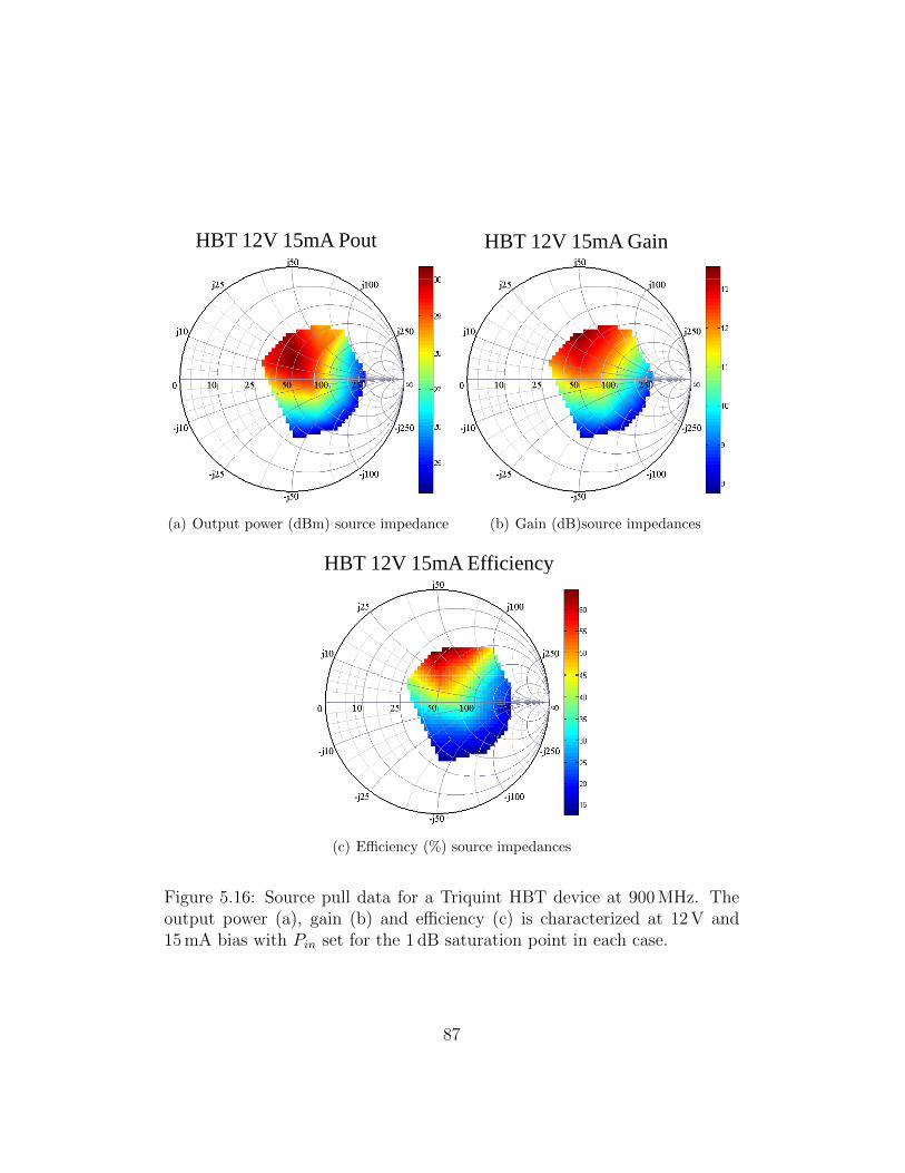
HBT 12V 100mA Gain HBT 12V 15mA Pout
HBT 12V 15mA Efficiency
(a) Output power (dBm) source impedance
HBT 12V 15mA Gain HBT 12V 15mA Pout
HBT 12V 15mA Efficiency
(b) Gain (dB)source impedances
HBT 12V 100mA Gain HBT 12V 15mA Pout
HBT 12V 15mA Efficiency
(c) Efficiency (%) source impedances
Figure 5.16: Source pull data for a Triquint HBT device at 900 MHz. Theoutput power (a), gain (b) and efficiency (c) is characterized at 12 V and15 mA bias with Pin set for the 1 dB saturation point in each case.
87

HBT 12V 100mA Gain HBT 12V 100mA Pout
HBT 12V 100mA Efficiency
(a) Output power (dBm) source impedances
HBT 12V 100mA Gain HBT 12V 100mA Pout
HBT 12V 100mA Efficiency
(b) Gain (dB) source impedances
HBT 12V 100mA Gain HBT 12V 100mA Pout
HBT 12V 100mA Efficiency
(c) Efficiency (%) source impeadnces
Figure 5.17: Source pull data for a Triquint HBT device at 900 MHz. Theoutput power (a), gain (b) and efficiency (c) is characterized at 12 V and100 mA bias with Pin set for the 1 dB saturation point in each case.
88

are smaller which correlates to a higher linearity as expected from the class
of operation. The 100 mA bias is close to a class-A load line, while the
15 mA corresponds closer to class-B operation, which has significant nonlinear
output voltage waveform.
Some interesting conclusions can be drawn from the measurements. From
Figure 5.18, we can conclude that a linear PA would have source impedance
in the range around ZS=10+j10 Ω. This point is not even covered by the gain
plot from Figure 5.16. Thus, at 15 mA the device is not linear and cannot be
optimized for gain simultaneously with linearity. If we are willing to drop the
gain by matching the input for linearity, then on the load side, the optimal
ACPR impedance of ZL=25+j30 Ω is not at the optimal power level and in
a design compromise would be made in power and linearity. For the class-A
100 mA bias, the gain also needs to be reduced for higher linearity, but load
impedance for best ACPR (ZL=25+j30)is very close to the optimal Pout load
at ZL=30+j30 Ω.
5.3.3 Error Vector Magnitude Results
The Error Vector Magnitude measurements were obtained from a signal with
the same standard IS-95 modulation and with a Quadrature Phase-Shift
Keying (QPSK) mapping in the I/Q plane. The results plotted on the Smith
chart in the following Figures are: EVM as a percentage defined by Equation
5.5 and EVM phase error (θ) illustrated in Figure 5.9. In addition, note that
the worst EVM for each bias point converges to the same impedance regions
89

ACPR Load Pull (10MHz spacing)HBT 12V 15mA ACPR
Pout=20dBmPout 20dBm
Pout=22dBm Pout=24dBm(a) ACPR(dBc) load impedances
ACPR Source Pull (10MHz spacing)Pout=20dBm
Pout=22dBm Pout=24dBm
HBT 12V 15mA ACPR
(b) ACPR(dBc) source impedances
Figure 5.18: ACPR load and source pull data for Triquint HBT device at900 MHz. The ACPR is characterized at 12 V and 15 mA bias with Pin setfor the 1 dB saturation point in each case.
90

ACPR Load Pull (10MHz spacing)HBT 12V 100mA ACPR
Pout=20dBm
Pout=22dBm Pout=24(a) ACPR(dBc) load impedancesACPR Source Pull (10MHz spacing)
HBT 12V 100mA ACPR
Pout=20dBm Pout=22dBm
Pout=24dBm
(b) ACPR(dBc) source impedances
Figure 5.19: ACPR load and source pull data for Triquint HBT device at900 MHz. The ACPR is characterized at 12 V and 100 mA bias with Pin setfor the 1 dB saturation point in each case.
91

on both the load and the source side. Interestingly enough, it is the same
region as the one obtained in the ACPR measurements. The data for both
bias points give the same impedance for low ACPR and EVM.
5.3.4 Additive Phase Noise Results
The large signal additive phase noise load and source pull measurements
were performed using the system setup explained earlier and developed for
the first time in this thesis. First, at each impedance point, the device was
driven at 1 dB compression point where the phase noise data was acquired.
The large signal NF results are illustrated in Figures 5.24 and 5.25. The
device with 100 mA shows smaller NF which relates to a higher linearity.
Moreover, the result conforms with the theoretical linearity based on the
amplifier’s operational region. With collector current at 100 mA, the device
is biased closer to the class A amplifier region which has the highest linearity.
In addition, signal NF versus input power was measured for both bias
conditions at Zsource = 10 + j0.13 Ω and Zload = 41.21 + j22.81 Ω, as shown
in Figure 5.26. As expected, the NF increased as higher input power levels
were applied and as the device was driven harder into compression. The
amplifier with a 15 mA bias current shows worse phase noise performance
even though at some Pin levels it manifests smaller NF . This is because the
100 mA amplifier is already in compression at these levels, while 15 mA one
is still in the linear region (not compressing yet). If we were to compare the
92

EVM Load Pull (10MHz spacing)HBT 12V 15mA EVM RMSAvg (%) HBT 12V 15mA Phase Error (°)g ( ) ( )
5
6
7
8
1.5
2
2.5
1
2
3
4
0.5
1
Pout(dBm) Pout(dBm)
HBT 12V 15mA EVM HBT 12V 15mA Phase Error
10 15 20 25 30 350
10 15 20 25 30 350
(a) EVM(%) load impedances
EVM Load Pull (10MHz spacing)HBT 12V 15mA EVM RMSAvg (%) HBT 12V 15mA Phase Error (°)g ( ) ( )
5
6
7
8
1.5
2
2.5
1
2
3
4
0.5
1
Pout(dBm) Pout(dBm)
HBT 12V 15mA EVM HBT 12V 15mA Phase Error
10 15 20 25 30 350
10 15 20 25 30 350
(b) EVM(o) load impedances
Figure 5.20: EVM load pull data for Triquint HBT device at 900 MHz. TheEVM rms average (a) and EVM phase error (b) is characterized at 12 V and15 mA bias with Pin set for the 1 dB saturation point in each case.
93
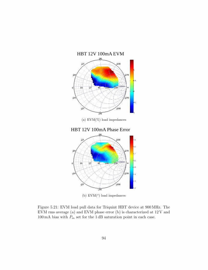
EVM Load Pull (10MHz spacing)HBT 12V 100mA EVM RMSAvg (%) HBT 12V 100mA Phase Error (°)
1.6
1.8
2
2.2
5
6
7g ( ) ( )
0.8
1
1.2
1.4
2
3
4
14 16 18 20 22 24 26 28 30
0 8
14 16 18 20 22 24 26 28 301
Pout(dBm) Pout(dBm)
HBT 12V 100mA EVM HBT 12V 100mA Phase Error
(a) EVM(%) load impedances
EVM Load Pull (10MHz spacing)HBT 12V 100mA EVM RMSAvg (%) HBT 12V 100mA Phase Error (°)
1.6
1.8
2
2.2
5
6
7g ( ) ( )
0.8
1
1.2
1.4
2
3
4
14 16 18 20 22 24 26 28 30
0 8
14 16 18 20 22 24 26 28 301
Pout(dBm) Pout(dBm)
HBT 12V 100mA EVM HBT 12V 100mA Phase Error
(b) EVM(o) load impedances
Figure 5.21: EVM load pull data for Triquint HBT device at 900 MHz. TheEVM rms average (a) and EVM phase error (b) is characterized at 12 V and100 mA bias with Pin set for the 1 dB saturation point in each case.
94

EVM Source Pull (10MHz spacing)HBT 12V 15mA EVM RMSAvg (%) HBT 12V 15mA Phase Error (°)g ( ) ( )
6
7
8
9
2.5
3
3.5
4
1
2
3
4
5
0.5
1
1.5
2
Pout(dBm) Pout(dBm)
HBT 12V 15mA EVM HBT 12V 15mA Phase Error
5 10 15 20 25 30 350
1
5 10 15 20 25 30 350
0 5
(a) EVM(%) source impedances
EVM Source Pull (10MHz spacing)HBT 12V 15mA EVM RMSAvg (%) HBT 12V 15mA Phase Error (°)g ( ) ( )
6
7
8
9
2.5
3
3.5
4
1
2
3
4
5
0.5
1
1.5
2
Pout(dBm) Pout(dBm)
HBT 12V 15mA EVM HBT 12V 15mA Phase Error
5 10 15 20 25 30 350
1
5 10 15 20 25 30 350
0 5
(b) EVM(o) source impedances
Figure 5.22: EVM source pull data for Triquint HBT device at 900 MHz.The EVM rms average (a) and EVM phase error (b) is characterized at 12 Vand 15 mA bias with Pin set for the 1 dB saturation point in each case.
95

EVM Source Pull (10MHz spacing)HBT 12V 100mA EVM RMSAvg (%) HBT 12V 100mA Phase Error (°)g ( ) ( )
2.5
3
3.5
6
7
8
9
1
1.5
2
2
3
4
5
Pout(dBm) Pout(dBm)
HBT 12V 100mA EVM HBT 12V 100mA Phase Error
5 10 15 20 25 30 350.5
5 10 15 20 25 30 351
(a) EVM(%) source impedances
EVM Source Pull (10MHz spacing)HBT 12V 100mA EVM RMSAvg (%) HBT 12V 100mA Phase Error (°)g ( ) ( )
2.5
3
3.5
6
7
8
9
1
1.5
2
2
3
4
5
Pout(dBm) Pout(dBm)
HBT 12V 100mA EVM HBT 12V 100mA Phase Error
5 10 15 20 25 30 350.5
5 10 15 20 25 30 351
(b) EVM(o) source impedances
Figure 5.23: EVM load pull data for Triquint HBT device at 900 MHz. TheEVM rms average (a) and EVM phase error (b) is characterized at 12 V and100 mA bias with Pin set for the 1 dB saturation point in each case.
96

HBT 12V 100mA NF HBT 12V 15mA NF
HBT 12V 100mA NF HBT 12V 15mA NF
(a) NF (dB) load impedances
HBT 12V 100mA NF HBT 12V 15mA NF
HBT 12V 100mA NF HBT 12V 15mA NF
(b) NF (dB) source impedances
Figure 5.24: Large signal NF load and source pull data for Triquint HBTdevice at 900 MHz. The NF is characterized at 12 V and 15 mA bias withPin set for the 1 dB saturation point in each case.
97

HBT 12V 100mA NF HBT 12V 15mA NF
HBT 12V 100mA NF HBT 12V 15mA NF
(a) NF(dB) load impedances
HBT 12V 100mA NF HBT 12V 15mA NF
HBT 12V 100mA NF HBT 12V 15mA NF
(b) NF(dB) source impedances
Figure 5.25: Large signal NF load and source pull data for Triquint HBTdevice at 900 MHz. The NF is characterized at 12 V and 100 mA bias withPin set for the 1 dB saturation point in each case.
98
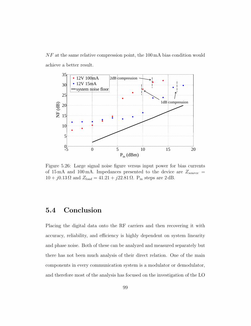
NF at the same relative compression point, the 100 mA bias condition would
achieve a better result.
30
35
12V 100mA12V 15mA
2dB compression
25system noise floor
1dB compression
15
201dB compression
NF
(dB
)
10
15N
0
5
-5 0 5 10 15 200
Pin (dBm)
Figure 5.26: Large signal noise figure versus input power for bias currentsof 15 mA and 100 mA. Impedances presented to the device are Zsource =10 + j0.13 Ω and Zload = 41.21 + j22.81 Ω. Pin steps are 2 dB.
5.4 Conclusion
Placing the digital data onto the RF carriers and then recovering it with
accuracy, reliability, and efficiency is highly dependent on system linearity
and phase noise. Both of these can be analyzed and measured separately but
there has not been much analysis of their direct relation. One of the main
components in every communication system is a modulator or demodulator,
and therefore most of the analysis has focused on the investigation of the LO
99

phase noise effect on the modulated signal [76],[77]. In work done in [76],
the authors estimate LO phase noise effects on EVM and adjacent channel
signals using a developed system model. Similarly author in [77] derives an
analytical expression given by:
EVMrms =
√1
SNR+ 2− 2exp
(−∆φ2
2
)(5.6)
where SNR is a signal to the noise ratio and ∆φ is rms LO phase error.
Moreover, another formula can be derived relating LO phase noise to
EVM [78]. Referring to Figure 5.9 and using Equation 5.5:
EVM =
√‖error vector‖2
‖reference vector‖2(5.7)
Using the relations in geometry EVM is calculated to be
EVM = 2sinθ
2(5.8)
where
θ =180
π
√∫ ∞∞
Sθ(f) df (5.9)
finally we get
EVM = 2sin
(28.7
√∫ ∞0
2Lθ(f) df
)(5.10)
where L is LO SSB phase noise.
The other main contributor to the distortion of the transmitted signal is
an amplifier. Its characterization is mainly done based on linearity standards
described earlier. So far, to the writer’s best knowledge, no one has tried to
combine an amplifier’s linearity performance and its additive phase noise.
100

Figure 5.27 illustrates power amplifier additive phase noise for the best and
the worst large signal noise figure load impedances at 12 V and 15 mA bias
condition. Using these two results and applying it to the Equation 5.10 we ob-
tain small EVM numbers, smaller than 1%. In comparisson to the measured
EVM results of 7%, this shows that the PA is not the main contributor to
the linearity in terms of EVM. Although, the calculated numbers are smaller
than measured, one cannot calculate the exact EVM performance based on
PA’s additive phase noise but definitely can find the impedance location that
will result in the best NF/EVM. Reviewing the load pull results obtained in
this chapter, it is obvious that that there is a relationship between the two.
For example, comparing the results from the EVM and the additive phase
noise measurements, both the load and the source impedances associated
with the best (and the worst) performances align closely. Similar pattern is
seen for ACPR results as well. Another observation from the obtained data
is that a “weakly” biased transistor shows a worse phase noise performance
which correlates to a worse linearity.
Using this information, one might not be able to directly predict linearity
performance, but one can certainly design for the best possible performance
by choosing the right impedance location based on the phase noise measure-
ment. Figure 5.28 summarizes the load pull impedances for 100 mA bias
condition. In order to have a more linear PA, sacrifice in Pout and Effi-
ciency have to be made. Note that EVM and NF results converge to the
same impedance locations on the Smith chart. Eventhough the best ACPR
101
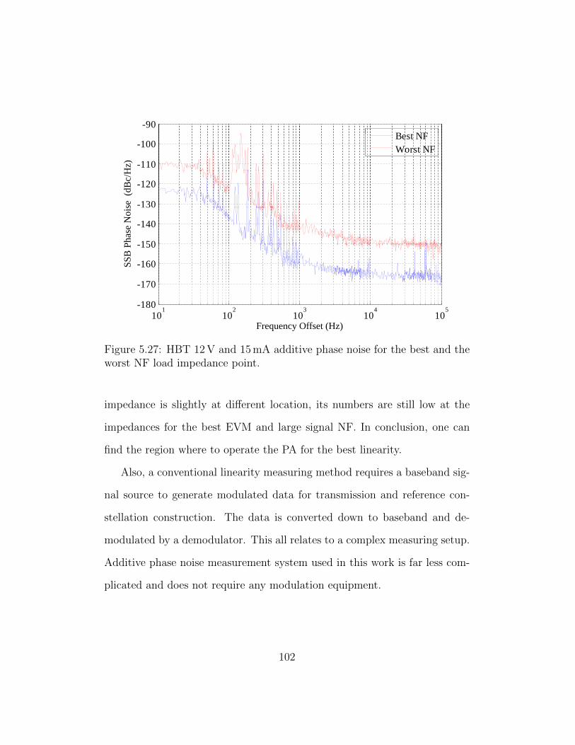
-90
B t NFH
z) -110
-100Best NFWorst NF
se (
dBc/
H
-130
-120
Phas
e N
ois
150
-140
SSB
P
170
-160
-150
101
102
103
104
105-180
-170
Frequency Offset (Hz)
Figure 5.27: HBT 12 V and 15 mA additive phase noise for the best and theworst NF load impedance point.
impedance is slightly at different location, its numbers are still low at the
impedances for the best EVM and large signal NF. In conclusion, one can
find the region where to operate the PA for the best linearity.
Also, a conventional linearity measuring method requires a baseband sig-
nal source to generate modulated data for transmission and reference con-
stellation construction. The data is converted down to baseband and de-
modulated by a demodulator. This all relates to a complex measuring setup.
Additive phase noise measurement system used in this work is far less com-
plicated and does not require any modulation equipment.
102

j50
j25 j100Efficiency Worst
Linearity j10 j250Pout
ACPR
Linearity
10 25 50 100 2500 ∞0 ∞0 ∞0 ∞0 ∞EVM
70-j10 -j250
NF
70mm
-j25 -j100
-j50
Figure 5.28: Summary of Load Pull impedances for Triquint HBT deviceat 900 MHz that is biased at 12 V and 100 mA. The plot shows the optimalimpedance values for Pout, Efficiency, ACPR, EVM and NF.
103

Chapter 6
Conclusions and Future Work
6.1 Thesis Summary and Contributions
The core of the work presented in this thesis is a method to characterize
phase noise of transistors operating in saturation over a range of power levels
in the microwave frequency range. Transistors operate in saturation in the
case of oscillators and power amplifiers, and the phase noise close to the
carrier frequency is examined in these two cases. Both oscillators and power
amplifiers are standard components in any communication or radar front end,
as indicated in Figure 6.1. The components of a front end that this thesis
focuses on in terms of phase noise characterization are shown in color in the
figure. In addition to phase noise, parameters that were considered for the
high-performance oscillator circuit designs were low power consumption, low
temperature coefficients, tunable frequency of operation and small physical

PowerA lifi
Low NoiseA lifi
IQ Modulation Demodulation
Mixer
Amplifier(PA)
Amplifier(LNA)
Mixer
Q
Additive Phase NoiseLocal Oscillator
Local Oscillator
Phase Noise(LO) (LO)
Figure 6.1: High-level microwave communications system block diagram in-cluding transmitter and receiver end. The main noise contributors in thesystem are shown in color. Minimizing noise increases system sensitivity andSNR.
size, as well as integration with a nonlinear non-standard load. In the case of
power amplifiers, high output power, efficiency and linearity were considered
as design goals in addition to known additive phase noise.
In oscillators, understanding how to characterize the phase noise has led
to a design methodology for very low phase noise and low power consumption
C-band oscillators for chip-scale atomic clocks. It is shown that small-signal
noise figure, typically provided by transistor manufacturers, is not a good
indicator of large-signal phase noise behavior. A relatively low-cost measure-
ment technique was thus developed for characterizing phase noise for stable
transistors operating in the large signal regime. From these measurements,
the large signal noise figure can be calculated, and the phase noise behav-
ior of the transistor in an oscillator circuit can be predicted. This allows
the designer to choose an appropriate transistor for oscillator design, as was
described in Chapter 3. A specific design at 3.4 GHz for a rubidium-based
105
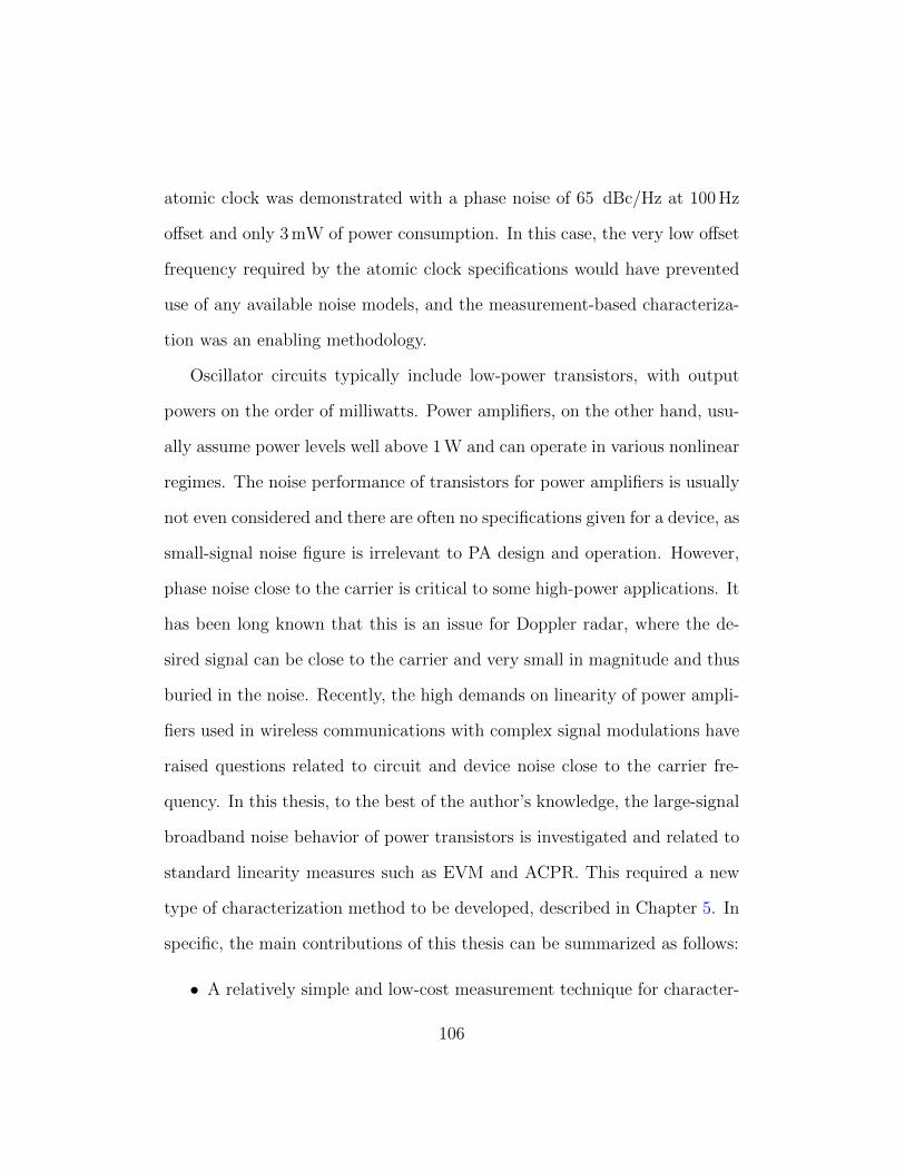
atomic clock was demonstrated with a phase noise of 65 dBc/Hz at 100 Hz
offset and only 3 mW of power consumption. In this case, the very low offset
frequency required by the atomic clock specifications would have prevented
use of any available noise models, and the measurement-based characteriza-
tion was an enabling methodology.
Oscillator circuits typically include low-power transistors, with output
powers on the order of milliwatts. Power amplifiers, on the other hand, usu-
ally assume power levels well above 1 W and can operate in various nonlinear
regimes. The noise performance of transistors for power amplifiers is usually
not even considered and there are often no specifications given for a device, as
small-signal noise figure is irrelevant to PA design and operation. However,
phase noise close to the carrier is critical to some high-power applications. It
has been long known that this is an issue for Doppler radar, where the de-
sired signal can be close to the carrier and very small in magnitude and thus
buried in the noise. Recently, the high demands on linearity of power ampli-
fiers used in wireless communications with complex signal modulations have
raised questions related to circuit and device noise close to the carrier fre-
quency. In this thesis, to the best of the author’s knowledge, the large-signal
broadband noise behavior of power transistors is investigated and related to
standard linearity measures such as EVM and ACPR. This required a new
type of characterization method to be developed, described in Chapter 5. In
specific, the main contributions of this thesis can be summarized as follows:
• A relatively simple and low-cost measurement technique for character-
106

izing large-signal noise figure of transistors in the microwave frequency
range is developed and used for a number of circuit designs. The appli-
cations range from ultra-low power oscillators for atomic clocks to high-
power amplifiers for wireless communications and radar transmitters.
The characterization method is reported in [40], and more recently
some parts of the method are also reported in [79]
• Relationship between large signal noise figure and phase noise close to
carrier. The results of this work are reported in [40].
• A design method for voltage controlled oscillators (VCOs) with simulta-
neous small size, low phase noise, DC power consumption, and thermal
drift is presented. Design steps are shown to give good prediction of
the VCO phase noise and power consumption behavior: (1) measured
resonator frequency-dependent parameters; (2) a transistor additive
phase noise/ noise figure characterization; (3) an accurate tuning ele-
ment model; and (4) a bias-dependent model in case of an active load.
As an illustration, the design of a 3.4 GHz bipolar transistor VCO with
varactor tuning is presented. Oscillator measurements demonstrate a
low phase noise with power consumption of a few milliwatts with a
circuit footprint smaller than 0.6 cm2. The results of this work are
reported in [3].
• The measurement technique was extended to power amplifiers. The re-
sults of this work are planned to be included in a paper to be submitted
107

in the near future.
• Relationship between additive phase noise and linearity in PAs with
modulated carriers. The results of this work are planned to be included
in a paper to be submitted in the near future.
6.2 Directions for Future Work
Several directions for possible future work that are enabled by the results
of this thesis are identified and preliminary results obtained. In the area of
oscillator design, injection locking by a lower-frequency clean signal is con-
sidered. Often microwave oscillators are stabilized with low-frequency (10s
of MHz) temperature-stabilized crystal oscillators. Advanced high-frequency
crystals are considered here as a possible path to sub-harmonic injection lock-
ing for extremely low phase noise microwave oscillators, as described below.
In the area of PA design, there is a need for broadband PAs covering octave
and decade bandwidths for various military platforms. It is important for
these applications that the PA is not only broadband, but also efficient due
to limited power availability in some applications. A preliminary PA broad-
band design was implemented and the additive phase noise characterized at
a selected frequency as a preliminary data point for discussion related to
implications on future broadband systems.
108

6.2.1 Injection-Locked Low Phase Noise Oscillators
Microwave oscillators can be stabilized by injection locking, which has been
described in detail by many authors, most notably Kurokawa in his classic
paper [80]. Briefly, a low phase noise master oscillator which is more than
20 dB below the main oscillator in power can be used to injection lock the
higher-power slave oscillator and reduce its noise to that of the cleaner oscil-
lator. Since this is a nonlinear process, the injected source can be at either
harmonics or subharmonics of the slave oscillator. Typically, the phase noise
of lower frequency oscillators can be made much better than that of higher
frequency microwave oscillators. The lowest phase noise devices are crys-
tal oscillators, especially if they include temperature stabilization. However,
common crystal oscillators are at MHz frequencies, up to possibly 100 MHz
but usually around 10 MHz.
In the process of designing the VCO in Chapter 3, a research–level crys-
tal resonator at 569 MHz was provided from Connor Winfield. This is the
sixth sub–harmonic of 3.41 GHz required frequency for the Rubidium Chip
Scale Atomic Clock Voltage Controlled Oscillator. A injection–locking mas-
ter crystal oscillator was designed at 569 MHz to investigate its applicability
to C–band VCOs. The measured phase noise is shown in Figure 6.2 Even
when multiplied by the standard 20logN = 20log6 = 15.56 factor, this oscilla-
tor is about 15 dB below in phase noise relative to the fundamental frequency
VCO from Chapter 4. Some directions for future work are:
109
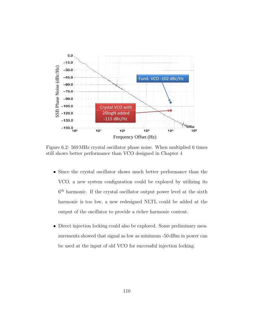
Hz)
Fund. VCO ‐102 dBc/Hz
ise
(dB
c/H
Crystal VCO with
B P
hase
No
20logN added‐115 dBc/HzSS
B
Frequency Offset (Hz)
Figure 6.2: 569 MHz crystal oscillator phase noise. When multiplied 6 timesstill shows better performance than VCO designed in Chapter 4
• Since the crystal oscillator shows much better performance than the
VCO, a new system configuration could be explored by utilizing its
6th harmonic. If the crystal oscillator output power level at the sixth
harmonic is too low, a new redesigned NLTL could be added at the
output of the oscillator to provide a richer harmonic content.
• Direct injection locking could also be explored. Some preliminary mea-
surements showed that signal as low as minimum -50 dBm in power can
be used at the input of old VCO for successful injection locking.
110

6.2.2 Phase Noise in Broadband and Efficient High
Power Amplifiers
The author designed a high power and high efficiency HBT power amplifier
that operates from 100 - 1000 MHz for use in communications systems and
broadband military platforms. It operates on 28 V DC and outputs 40 W with
a collector efficiency higher than 58 % across decade of frequency bandwidth.
PA was fabricated using TriQuint’s HBT Transistor T1H2005028-SP with
the performance shown in Figure 6.3.
PA Design
Since no data was available for this devices, the author had to find optimal
impedances to present to the device in order to accomplish the best perfor-
mance. A basic load pull measurement was performed at every 100 MHz. The
obtained data is plotted on the Smith chart in Figure 6.4. The data shows
the matching impedances for the highest output power, the best efficiency,
and the compromise between the two.
Next, input and output fixture were designed based on the optimal impe-
dances acquired during the load pull testing. The microstrip tapered line
was chosen as the input matching circuit. The taper layout was simulated
in Matlab using the code based on a theory of small reflections of the mul-
tisectional tapered line [81],[82]. Final layout was simulated and verified in
Momentum, 3D planar electromagnetic simulator from Agilent EEsof EDA.
111
100 200 300 400 500 600 700 800 900 10000
5
10
15
20
25
30
35
40
45
50
55
60
65
70
Frequency (MHz)
T1H2005028-SP 100MHz-1000MHz 28V 50mA
Gain (dB)Pout (dBm)Collector Efficiency (%)PAE (%)
Figure 6.3: PA performance in fixture. Power output is 40 W with efficiencyhigher than 58 % across the whole bandwidth.
The final impedance presented by tapered line is shown in Figure 6.4.
The output matching circuit is made of a Transmission Line Transformer
(TLT) using three 90 mm coaxial lines with 15 Ω characteristic impedance.
These devices transform current, voltage and impedances like conventional
wire-wound transformers [83],[84]. Impedance transformation realized with
TLTs is based on splitting and recombining transmission lines [85]. In this
112

1 2.5 5 10 25
j1
-j1
0 ∞
j2.5
-j2.5
0 ∞
j5
-j5
0 ∞
j10
-j10
0 ∞
j25
-j25
0 ∞
100MHz
1000MHz
100MHz
100MHz
1000MHz 1000MHz
1000MHz
Zout FixtureZin FixtureZin CompromiseZout CompromiseZout for PoutZout for Efficiency
Figure 6.4: Device load pull data results. Optimal impedance locations areillustrated. Also plotted are input and output fixture responses.
case three coaxial lines with a characteristic impedances of 15 Ω are combined
in series at high impedance end and in parallel at the other low-impedance
end [86]. With this configuration, impedance ratio of approximately 1:9
was achieved. Different equal lengths of cables were built and measured
and 90 mm long exhibited best impedance matching performance for the
particular design. The measured impedances of the final output matching
circuit design is plotted in Figure 6.4.
113

The bias circuit for the PA was designed using lumped components, with
a Colicraft 120 nH inductor as the RF choke at input. Since current flowing
through the collector was much higher (up to 4 A), a custom wound inductor
was built for the output end. A 2500 pF broadband capacitor was utilized
as a DC block. Additional capacitor banks were added in parallel to bias
lines to short out any RF leakage and avoid lower frequency oscillations. A
photograph of the finished PA fixture is shown in Figure 6.5
7070mm
Figure 6.5: Broadband PA fixture design.
114

PA Phase Noise
Using the technique developed in this thesis, the additive phase noise of
a broadband PA was measured. The large signal NF was calculated and
plotted in Figure 6.6. As the power input is increased, the NF becomes
larger. These results confirm that a large signal NF is indeed much higher
than expected. Also, notice the rapid increase of the NF as the PA starts to
compress around Pin = 31 dBm. This is explained by higher nonlinearities as
device enters the compression region. This can also been seen in the phase
noise measurements of smaller device discussed in this chapter, Figure 5.26.
50
60
28V 50mA HBTsystem noise floor
2dB compression
40
50 system noise floor1dB compression
30
NF
(dB
)
10
20
N
5 10 15 20 25 30 35 400
10
5 10 15 20 25 30 35 40Pin (dBm)
Figure 6.6: Broadband PA large signal noise figure.
Related future work:
• The analysis of additive phase noise could be implemented in broad-
115

band design. Load/source pull measurements can be performed to
find optimal points for low additive phase noise which would lead to a
higher linearity. With this information, current amplifier layout could
be redesigned to achieve better linearity performance as well.
• In addition, the 2nd harmonic load/source pull analysis could be inves-
tigated. These results could further examine the relationship between
linearity and additive phase noise.
• Investigate PA sensitivity to bias noise and characterize DC supplies
based on PA noise tolerance.
6.3 Final Conclusions
In conclusion, this thesis focuses a method to characterize phase noise of tran-
sistors operating in saturation over a range of power levels in the microwave
frequency range. An experimentally-based technique for predicting phase
noise close to the carrier frequency was developed as a combination of phase
noise and load-pull measurement systems. In this thesis, the Holzworth In-
strumentation phase noise setup was combined with a Focus Microwave load
pull system, and the author is grateful to Dr. Jason Breitbarth (Holzworth
Instrumentation) and Mr. William McCalpin (TriQuint) for the use of the
instruments.
Some useful conclusions from applying the measurement system to various
116

circuits are made and were used for several high-performance circuits in L
and C bands. For example, the measurement technique was employed for
characterizing phase noise for stable transistors operating in the large signal
regime. From these measurements, the phase noise behavior of the transistor
in an oscillator circuit can be predicted. This conclusion was validated on
a specific oscillator design at 3.4 GHz for a rubidium-based atomic with a
demonstrated phase noise of 65 dBc/Hz at 100 Hz offset and only 3 mW of
power consumption. In this case, the very low offset frequency required by
the atomic clock specifications would have prevented use of any available
noise models, and the measurement-based characterization was an enabling
methodology.
The final conclusions of this thesis relate to power amplifiers, and are
valid for much higher power levels and different devices than in the oscil-
lator case. Phase noise close to the carrier is critical to some high-power
applications, such as Doppler radar and wireless communications with com-
plex signal modulations. In this thesis, the measurement system developed
for general additive phase noise characterization was modified for PA de-
sign. An investigation of the large-signal broadband noise behavior of power
transistors enabled investigation of the relationship between phase noise and
standard linearity measures such as EVM and ACPR. As communication
signals become more complex and out-of-band linearity more critical, it is
expected that the characterization developed in this thesis will increasingly
become a necessary part of transmitter power amplifier design.
117

Bibliography
[1] E. S. Ferre-Pikal F. L. Walls, “Measurement of Frequency, Phase Noiseand Amplitude Noise,” Wiley Encyclopedia of Electrical Engineers, vol.12, pp. 459–473, 1999. xiv, 32
[2] A. Brannon, Design And Implementation of Microwave VCOs For Chip-scale Atomic Clocks, Ph.D. thesis, Department of Electrical Engineer-ing, University of Colorado, Boulder, 2007. xvi, 47
[3] M. Jankovic, A. Brannon, J. Breitbarth, and Z. Popovic, “Designmethod for low-power, low-phase noise voltage-controlled oscillators,”in 37th European Microwave Conference (EuMC), October 2007. xvii,28, 53, 58, 59, 62, 107
[4] J. Breitbarth, S. Pajic, N. Wang, and Z. Popovic, “Additive phase noisein linear and high-efficiency x-band power amplifiers,” in IEEE MTT-SInternational Microwave Symposium Digest, June 2006, pp. 1871–1874.xviii, 64, 69, 70, 71
[5] H. Hausman, “Estimate multiple carrier interferance,” in Microwaves& RF, May 2004. xix, 74
118

[6] Holzworth Instrumentation, HS1004 Web Data Sheet. xix, 81
[7] M. S. Gupta, Electrical Noise: Fundamentals and Sources, IEEE Press,New York, 1977. 1
[8] Sigfrid Yngvesson, Microwave Semiconductor Devices, Kluwer Aca-demic Publishers, 1991. 1
[9] X. Zhu K. H. Duh A. Van der Ziel, P. H. Handel, Noise in Solid StateDevices and Circuits, John Wiley, New York, 1986. 2
[10] James A. Barnes, Andrew R. Chi, Leonard S. Cutler, Daniel J. Healey,David B. Leeson, Thomas E. McGunigal, James A. Mullen, Warren L.Smith, Richard L. Sydnor adn Robert F. C. Vessot, and Gernot M. R.Winkler, “Characterization of Frequency Stability,” IEEE Transactionson Instrumentation and Measurement, vol. 20, no. 2, pp. 105–120, 1971.3, 7
[11] D. Halford J. H. Shoaf and A. Risley, “Frequency Stability Specificationsand Measurement: High Frequency and Microwave Signals,” NationalBureau of Standards (US) Technical Note 632, vol. 1, pp. 40–46, January1973. 3, 19
[12] Agilent Product Note 11729C-2, Phase Noise Characterization of Mi-crowave Oscillators, Frequency Discriminator Method. 3, 18, 21, 59
[13] F. L. Walls, “Correlation between upper and lower noise sidebands,” inIEEE International Frequency Control Symposium, 1998. 5, 8
119

[14] W. P. Robins, Phase Noise in Signal Sources (Theroy and applications),IEE Telecommunications Series 9. Peter Peregrinus Ltd., London, UK,1982. 6, 8, 11
[15] Michael Lombardi, The Mechatronics Handbook, CRC Press LLC, 2002.7
[16] F. L. Walls D. Walker A. Haiti, D. A. Howe, “Noise figure vs. PMnoise measurements,” in Proceeddings of IEEE International FrequencySymposium, 2003, pp. 516–520. 8, 31, 51, 52
[17] F. L. Walls E. S. Ferre-Pikal and C. W. Nelson, “Guidelines for designingBJT amplifiers with low 1/f AM and PM noise,” IEEE Trans. Ultrason.,Ferroelect., Freq. Control, vol. 44, pp. 335–343, March 1997. 8
[18] E. S. Ferre-Pikal F. L. Walls and S. R. Jefferts, “Origin of 1/f PM noiseand AM noise in bipolar junction transistor amplifiers,” IEEE Trans.Ultrason., Ferroelect., Freq. Control, vol. 44, pp. 326–334, March 1997.9
[19] J. B. Johnson, “The schottky effect in low frequency circuits,” Phys.Rev., vol. 26, no. 1, pp. 71–85, July 1925. 9
[20] W. Schottky, “Small-shot effect and flicker effect,” Phys. Rev., vol. 28,no. 1, pp. 74, July 1926. 9
[21] M. S. Keshner, “1/f Noise,” in Proceedings of the IEEE, March 1982,vol. 70, pp. 212–218. 9
120

[22] E.S. Ferre F. G. Ascarrunz, A. Zhang and F. L. Walls, “PM noisegenrated by noise components,” IEEE International Frequency ControlSymposium, vol. 1, pp. 210–217, 1998. 9
[23] D. Scherer, “Today’s lesson: Learn about low noise design, part 1,” inMicrowaves, April 1979, pp. 116–122. 9, 40
[24] G. Sauvage, “Phase noise in oscillators: A mathematical analysis ofleeson’s model,” in IEEE Transactions on Instrumentation and Mea-surement, December 1977, pp. 408–410. 9
[25] T. E. Parker, “Characteristics and sources of phase noise in stableoscillators,” in 41st Annual Frequency Control Symposium, 1987, pp.99–110. 9
[26] J. Rutman and F. L. Walls, “Characterization of frequency stability inprecision frequency sources,” in Proceedings of the IEEE, June 1991,vol. 71, pp. 952–960. 11
[27] M. Kolber, “Predict phase noise effects in digital communications sys-tems,” Microwaves and RF, vol. 210, pp. 59–70, September 1999. 12
[28] S. A. Cardero, “Calculate the effect of RF building block on AM andPM noise,” Microwaves and RF, vol. 236, pp. 56–63, 2000. 12
[29] Andrew Richardson, WCDMA Design Handbook, Cambridge UniversityPress, 2005. 13
121

[30] D. K. Barton, Radar System Analysis and Modeling, Artech House,2005. 14
[31] W. D. Seal A. L. Lance and F. Labaar, “Phase noise and AM noiseand measurements in the frequency domain,” Infrared and MillimeterWaves, vol. 11, pp. 239–289, 1984. 19, 21, 32
[32] C. Nelson J. Li, E. Ferre-Pikel and F. L. Walls, “Review of PM and AMnoise measurement systems,” in Proceeddings of IEEE InternationalFrequency Symposium, 1998, pp. 197–200. 19
[33] W. B. Bruene E. W. Pappenfuss and E. O. Schoenike, Single SidebandPrinciples and Ciruits, New York: McGraw Hill, 1964. 22
[34] D. L. Cheadle, “Selecting mixers for best intermod performance,” Mi-crowaves, vol. 12, pp. 48–54, 58–62, 1973. 23
[35] S. R. Kurtz, “Mixers as phase detectors,” Watkins Johnson TechnicalNotes, vol. 5, pp. 1–16, 1978. 23, 28
[36] J. G. Ondria, “A microwave system for measurements of AM and FMnoise spectra,” in IEEE Trans. Microwave Theory and Techniques,MTT-16, 1968, pp. 767–781. 23
[37] C.B. S Scarles J.R. Ashley and F. M. Palk, “The measurement of oscilla-tor noise at microwave frequencies,” in IEEE Trans. Microwave Theoryand Techniques, MTT-16, 1968, pp. 753–760. 23
122

[38] A. Tykulsky, “Spectral measurements of oscillators,” in Proceedings ofIEEE 54, 1966. 24
[39] D. Halford, “The Delay Line Discriminator,” National Bureau of Stan-dards (US) Technical Note 10, vol. 1, pp. 19–38, 1975. 24
[40] M. Jankovic, J. Breitbarth, A. Brannon, and Z. Popovic, “Measuringtransistor large-signal noise figure for low-power and low-phase noiseosscilator design,” IEEE Transactions on Microwave Theory and Tech-niques, vol. 56, no. 7, pp. 1511–1515, July 2008. 28, 107
[41] Steve C. Cripps, RF Power Amplifiers For Wireless Communications,Artech House, 2006. 30, 63
[42] Guillermo Gonzalez, Microwave Transistor Amplifiers: Analysis andDesign, Prentice Hall, 1996. 30
[43] J. Portilla N. Garmendia, “Study of PM noise figure in low noise ampli-fiers working under small and large signal conditions,” in IEEE MTT-SInternational Microwave Symposium Digest, June 2007. 31, 33
[44] J. Breitbarth, Design and Characterization of Low Phase Noise Mi-crowave Circuits, Ph.D. thesis, Department of Electrical Engineering,University of Colorado, Boulder, 2006. 38, 52
[45] R. Yu M. Chase E. Carman M. J. W. Rodwell, M. Kamegawa and K. S.Giboney, “GaAs nonlinear transmission lines for picosecond pulse gen-eration and milimeter wave sampling,” IEEE Trans. Microwave Theoryand Techniques, vol. 39, no. 7, pp. 1194–1204, July 1991. 39
123

[46] M. Case M. Kamegawa R. Yu M. J. W. Rodwell E. Carmand, K. Gi-boney and J. Franklin, “28-39 GHz distributed harmonic generationon solition nonlinearr transmission line,” IEEE Microwave and GuidedWave Lett., vol. 1, no. 2, pp. 28–31, February 1991. 39
[47] D. Salameh and D. Linton, “Microstrip GaAs nonlinear transmission-line (NLTL) harmonic and pulse generators,” IEEE Trans. MicrowaveTheory and Techniques, vol. 47, no. 7, pp. 1118–1121, July 1999. 39
[48] M. G. Chase, Nonlinear transmission line picosecond pulse, impulseand milimeter-wave harmonic generation, Ph.D. thesis, University ofCalifornia, Santa Barbara, 1993. 39
[49] E. Afshari and A. Hajmiri, “Non-linear transmission lines for pulseshaping in silicon,” in IEEE Custom Integrated Circuits Conference,2003, pp. 91–94. 39
[50] M. Fernandez A. Jrad X. Melique J. Tao S. Arscott D. LippensJ. M. Duchamp, P. Ferrari and R. G. Harrison, “Comparison of fullydistributed and periodically loaded nonlinear transmission lines,” IEEETrans. Microwave Theory and Techniques, vol. 51, no. 4, pp. 1105–1116,April 2003. 40
[51] Z. Popovic A. Brannon, J. Breitbarth, “A low power, low phase noiselocal oscillator for chip-scale atomic clocks,” in IEEE MTT-S Interna-tional Microwave Symposium Digest, June 2005, pp. 1535–1538. 40, 49,53, 58, 61
[52] F. M. Stern and J. Dowsett, “The fabrication of high frequency fun-
124

damental crystals by plasma etching,” in 43rd Annual Symposium onFrequency Control, 1989. 44
[53] H. Uehara M. Umeki, T. Sato and M. Okazaki, “622mhz high frequencyfundamental composite crystal resonator with an air-gapped electrode,”in 2004 IEEE International Ultrasonics, Ferroelectrics, and FrequencyControl Joint 59th Anniversary Conference, 2004. 44
[54] M. S. Patel and Y. K. Yong, “Conceptual design of high-q, 3.4-ghzthin film quartz resonator,” in IEEE Transaction on Ultrasonics, Fer-roelectrics, and Frequency Control, 2009, vol. 56, pp. 912–920. 44
[55] P. D. D. Schwindt V. Shah L. Liew J. Moreland H. G. Robinson A.Brannon J. Breitbarth Z. Popovic L. Hollberg J. Kitching V.Gerginov,S. Knappe, “Component level demonstration of a microfabricatedatomic frequency reference,” in Proceedings of the IEEE Joint Intnl.FCS and PTTI Systems and Applications Meeting, 2005, pp. 758–766.46
[56] P. D. D. Schwindt L. Hollberg J. Kitching L.A Liew S. Knappe, V. Shahand J. Moreland, “A microfabricated atomic clock:,” Applied PhysicsLetters, vol. 85, pp. 1460–1462, 2004. 46
[57] R. Lutwak, Pl. Vlitas, M. Varghese, M. Mescher, D. K. Serkland, andG. M. Peake, “The MAC - a miniature atomic clock:,” in Joint Meet-ing of the IEEE Intern. Frequency Control Symposium and the PTTISystems and Applications Meeting, 2005. 46
[58] S. Knappe J. Kitching and L. Hollberg, “Miniature vapor-cell atomic-
125

frequency references,” Applied Physics Letters, vol. 81, pp. 553–555,2002. 47
[59] S. Knappe, “MEMS atomic clocks,” in Comprehensive Micro-Systems,2007. 49
[60] D. Kajfez and E.J. Hwan, “Q-factor measurement with network ana-lyzer,” IEEE Trans. Microwave Theory and Techniques, vol. 32, pp.666–670, July 1984. 50
[61] L. S. Cutler and C. L. Searle, “Some aspects of the theory and measure-ments of frequency fluctuations in frequency standards,” in Proceedingsof the IEEE, February 1966, vol. 54, pp. 136–154. 51
[62] D.B. Leeson, “A simple model of feedback oscillator noise spectrum,”in Proceeding Letters, February 1966, pp. 329–330. 51
[63] G. H. Stauffer, “Finding the lumped element varactor diode model,” inHigh Frequency Electronics, Summit Technical Media, 2003. 53, 55
[64] S. Alechno, “Analysis method characterizes microwave oscillators, 4-part series,” Microwaves & RF Design, vol. 36, pp. 82–86, November1997. 56
[65] F. G. Ascarrunz, E. S. Ferre, and F. L. Walls, “Investigations of AM andPM noise in x-band devices,” in IEEE International Frequency ControlSymposium, 1993, pp. 303–311. 64
126

[66] O. Llopis, J. B. Juraver, B. Tamen, F. Danneville, M. Chaubet,A. Cappy, and J. Graffeui, “Nonlinear noise modeling of a phemt devicethrough residual phase noise and low frequency noise measurements,”IEEE Trans. Microwave Theory and Techniques, vol. 1, pp. 831–834,2001. 64, 70
[67] M. Rudolph and P. Heymann, “The influence of microwave two-portnoise on residual phase noise in GaAs-HBTs,” in 34th European Mi-crowave Conference, 2004, pp. 945–948. 64, 70
[68] B. Hughes, A. Ferrero, and A. Cognata, “Accurate on-wafer power andharmonic measurement of mm-wave amplifiers and devices,” in IEEEMTT-S International Symposium Digest, 1992, pp. 1019–1022. 67
[69] D. D. Poulin, J. R. Mahon, and J. P. Lanteri, “A high power on-wafer pulsed active load pull system,” IEEE Transactions on MicrowaveTheory and Techniques, vol. 40, pp. 2412–2417, 1992. 67
[70] Focus Microwaves, Measurement System Operational Manual, 1999. 67
[71] P. A. Dallas and J. K. A. Everard, “Measurement of the cross-correlation between baseband and transposed flicker noises in a [g]a[a]s[mesfet],” in IEEE MTT-S International Microwave Symposium Digest,1990, pp. 1261–1264. 70
[72] Anritsu Apllication Note, Intermodulation Distortion (IMD) Measure-ments. 74
127

[73] Narisi Wang, X-Band Class-E Power Amplifers with Dynamic BiasControl, Ph.D. thesis, University of Colorado, 2006. 74
[74] Agilent Product Note AN 1311, Understanding CDMA Measrementsfor Base Stations and Their Componenets. 76
[75] William McCalpin Triquint Semiconductor, Personal Communications(device still not commercial). 83
[76] T. Nakagawa and K. Araki, “Effects of phase noise on RF communica-tion signals,” in IEEE VTC’00, 2000, vol. 2, pp. 588–591. 100
[77] A. Georgiadis, “Gain, phase imbalance, and phase noise effects on errorvector magnitude,” in IEEE Transactions on Vehicular Technology,March 2004, vol. 53, pp. 443–449. 100
[78] S. He, X. Yan, and J.Bao, “Microwave oscillator phase noise require-ments for TD-SCDMA wireless communication systems,” in Journal ofElectronic Science and Technology of China, 2007. 100
[79] J. Breitbarth, M. Jankovic, and Z. Popovic, “Phase noise in varactornonlinear transmission-line frequency multipliers,” IEEE Trans. Mi-crowave Theory and Techniques, to be submitted April 2010. 107
[80] Kaneyuki Kurokawa, “Injection locking of microwave solid-state oscil-lators,” in Proceedings of IEEE, October 1973, vol. 61. 109
128

[81] R. E. Collin, “The optimal tapered transmission line matching section,”in Proc. IRE, 1956, vol. 44, pp. 539–548. 111
[82] R. E. Collin, Fundamentals for Microwave Engineering, McGraw-Hill,N.Y, second edition edition, 1992. 111
[83] G. Guanella, “New method of impedance matching in radio-frequencycircuits,” in Brown Boveri Review, Sept. 1944, pp. 327–329. 112
[84] J. Walker, D. Myer, F. Raab, and C. Trask, Classic Works in RF Engi-neering Combiners, Couplers, TRansformers, And MAgnetic Materials,Artech House, 2006. 112
[85] J. Sevick, Transmission Line Trasformers, SciTech Publishing, Inc.,2001. 112
[86] J. Horn and G. Boeck, “Ultra broadband ferrite transmission line trans-former,” in IEEE MTT-S Digest, 2003, pp. 433–436. 113
129