Phase Contrast Microscopy with Soft and Hard X-rays Using a
223
Phase Contrast Microscopy with Soft and Hard X-rays Using a Segmented Detector A Dissertation Presented by Benjamin Hornberger to The Graduate School in Partial Fulfillment of the Requirements for the Degree of Doctor of Philosophy in Physics Stony Brook University May 2007
Transcript of Phase Contrast Microscopy with Soft and Hard X-rays Using a

Phase Contrast Microscopy with Soft
and Hard X-rays Using a Segmented
Detector
A Dissertation Presented
by
Benjamin Hornberger
to
The Graduate School
in Partial Fulfillment of the Requirements
for the Degree of
Doctor of Philosophy
in
Physics
Stony Brook University
May 2007

Stony Brook University
The Graduate School
Benjamin Hornberger
We, the dissertation committee for the above candidate for the Doctor ofPhilosophy degree, hereby recommend acceptance of this dissertation.
Chris J. JacobsenProfessor, Department of Physics and Astronomy
Axel DreesProfessor, Department of Physics and Astronomy
Alfred S. GoldhaberProfessor, Department of Physics and Astronomy
Pavel RehakSenior Scientist, Brookhaven National Laboratory
This dissertation is accepted by the Graduate School.
Graduate School
ii

Abstract of the Dissertation
Phase Contrast Microscopy with Soft andHard X-rays Using a Segmented Detector
by
Benjamin Hornberger
Doctor of Philosophy
in
Physics
Stony Brook University
2007
Scanning x-ray microscopes and microprobes are unique tools forthe nanoscale investigation of specimens from the biological, envi-ronmental, biomedical, materials and other fields of sciences. Inthe soft x-ray range (below 1 keV photon energy), thus far theyconcentrate on studying chemical speciation of light elements byx-ray absorption near-edge structure (XANES) measurements. Inthe hard x-ray range (multi-keV), the main focus lies on trace ele-ment mapping by x-ray fluorescence.
Phase contrast provides a complementary contrast mechanism toabsorption and fluorescence. In the soft x-ray range, it can helpreduce the radiation dose imposed on the specimen by imaging be-low an absorption edge where absorption is low, but appreciablephase resonances occur. For harder x-rays, phase contrast allowsthe imaging of light elements which absorb very weakly at thosephoton energies. Therefore it provides a means to map the ul-trastructure of biological specimens and put trace elements intotheir cellular context. In particular, there is a strong demand for
iii
quantitative measurements of ultrastructure to obtain trace ele-ment concentrations rather than absolute amounts.
A segmented detector can be used to image the phase of the speci-men in a scanning microscope or microprobe. This is done by mea-suring the redistribution of intensity in the detector plane causedby phase gradients in the specimen. This thesis work describesthe application of a segmented detector in the soft x-ray range,and its further advancement for use with hard x-rays. Differentialphase contrast, obtained from simple difference images of opposingdetector segments, is easy to obtain even in real-time and is use-ful for a qualitative overview of specimen phase. Furthermore, wedescribe the application of a Fourier filtering algorithm to obtainquantitative maps of specimen amplitude and phase, from whichthe specimen mass can be inferred. Software for inspection andquantitative analysis of x-ray microscopy data is also presented.
iv

Contents
List of Figures ix
List of Tables xii
Acknowledgements xiii
1 Introduction 11.1 X-ray Interactions with Matter . . . . . . . . . . . . . . . . . 3
1.1.1 Absorption and Scattering Cross Sections . . . . . . . . 31.1.2 Atomic Scattering Factors and the Index of Refraction 51.1.3 Wave Propagation in Matter . . . . . . . . . . . . . . . 71.1.4 The Kramers-Kronig Relations . . . . . . . . . . . . . 91.1.5 Absorption and Emission Processes – X-ray Fluorescence 10
1.2 X-ray Microscopy . . . . . . . . . . . . . . . . . . . . . . . . . 131.2.1 Synchrotron Radiation Sources . . . . . . . . . . . . . 131.2.2 Types of X-ray Microscopes . . . . . . . . . . . . . . . 141.2.3 X-ray Optics – Fresnel Zone Plates . . . . . . . . . . . 161.2.4 Description of Instruments . . . . . . . . . . . . . . . . 20
1.3 Image Contrast in Scanning X-ray Microscopy . . . . . . . . . 221.3.1 Photon Statistics . . . . . . . . . . . . . . . . . . . . . 221.3.2 Absorption Contrast . . . . . . . . . . . . . . . . . . . 231.3.3 Phase Contrast . . . . . . . . . . . . . . . . . . . . . . 251.3.4 Fluorescence Contrast . . . . . . . . . . . . . . . . . . 251.3.5 Dark-Field Contrast . . . . . . . . . . . . . . . . . . . 26
1.4 Phase Contrast in X-ray Microscopy . . . . . . . . . . . . . . 271.4.1 Motivation – Why Measure Phase Contrast . . . . . . 271.4.2 Configured Detectors for Phase Contrast Imaging in a
Scanning Microscope . . . . . . . . . . . . . . . . . . . 301.4.3 Other Phase Contrast Techniques . . . . . . . . . . . . 31
v

2 A Segmented Silicon Detector for Hard X-ray Microprobes 322.1 Requirements for a Transmission Detector in Scanning X-ray
Microscopes and Microprobes . . . . . . . . . . . . . . . . . . 332.2 Review: The Existing Segmented Silicon Detector . . . . . . . 362.3 Limitations of the Existing Detector for Hard X-ray Microscopy 362.4 Segmented Silicon Chip . . . . . . . . . . . . . . . . . . . . . . 38
2.4.1 Photodiode Principle . . . . . . . . . . . . . . . . . . . 382.4.2 X-ray Absorption in Silicon and Chip Quantum Efficiency 392.4.3 Chip Design and Production . . . . . . . . . . . . . . . 402.4.4 Bias Voltage, Front- and Back-Side Illumination, and
Leakage Current . . . . . . . . . . . . . . . . . . . . . 432.4.5 Effects of Insufficient Bias Voltage . . . . . . . . . . . . 462.4.6 Radiation Damage . . . . . . . . . . . . . . . . . . . . 562.4.7 Visible Light Sensitivity . . . . . . . . . . . . . . . . . 60
2.5 Charge Integrating Electronics . . . . . . . . . . . . . . . . . . 612.5.1 Operating Principle . . . . . . . . . . . . . . . . . . . . 612.5.2 Dynamic Range Calculations . . . . . . . . . . . . . . . 622.5.3 Detector Timing and the Integration Cycle . . . . . . . 642.5.4 Interfacing with Microscope / Microprobe Electronics . 662.5.5 Noise Performance and Dynamic Range . . . . . . . . . 702.5.6 Linearity . . . . . . . . . . . . . . . . . . . . . . . . . . 71
2.6 Detector Calibration . . . . . . . . . . . . . . . . . . . . . . . 722.6.1 Detector Channel Crosstalk . . . . . . . . . . . . . . . 732.6.2 Voltage to Photon Flux Conversion . . . . . . . . . . . 752.6.3 Calibration Procedure and Software . . . . . . . . . . . 762.6.4 Verification of the Calibration . . . . . . . . . . . . . . 79
2.7 Detector Components . . . . . . . . . . . . . . . . . . . . . . . 79
3 Differential Phase Contrast 823.1 Signal to Noise Ratio in Absorption and Differential Phase Con-
trast in the Refraction Model . . . . . . . . . . . . . . . . . . 833.1.1 Signal to Noise Ratio in Absorption Contrast . . . . . 833.1.2 Signal to Noise Ratio in Differential Phase Contrast . . 853.1.3 Comparison of Absorption and Differential Phase Contrast 87
3.2 Differential Phase Contrast Examples . . . . . . . . . . . . . . 883.2.1 Combination with Fluorescence . . . . . . . . . . . . . 88
3.3 Benefits and Shortcomings of Differential Phase Contrast atHigh X-ray Energies . . . . . . . . . . . . . . . . . . . . . . . 94
3.4 Integration of the DPC Signal . . . . . . . . . . . . . . . . . . 943.4.1 Derivation of the Reconstruction Formula . . . . . . . 943.4.2 Simulations with Noise-free Data . . . . . . . . . . . . 97
vi

3.4.3 Simulations with Noisy Data . . . . . . . . . . . . . . . 973.4.4 Integration of Real Data . . . . . . . . . . . . . . . . . 993.4.5 Conclusions . . . . . . . . . . . . . . . . . . . . . . . . 101
4 Quantitative Amplitude and Phase Reconstruction from Seg-mented Detector Data 1024.1 Image Formation in a Scanning Transmission X-ray Microscope 103
4.1.1 Wave Propagation to the Detector Plane . . . . . . . . 1034.1.2 Comparison with the Refraction Model . . . . . . . . . 1064.1.3 Large-area Detector: Incoherent Imaging . . . . . . . . 1094.1.4 Point Detector: Coherent Imaging . . . . . . . . . . . . 1104.1.5 The Principle of Reciprocity . . . . . . . . . . . . . . . 1104.1.6 Segmented Detector: Partially Coherent Imaging . . . 1114.1.7 Details on the Weak Specimen Approximation . . . . . 112
4.2 Calculated Contrast Transfer Functions . . . . . . . . . . . . . 1134.2.1 Transfer Functions for Soft X-ray Experiments . . . . . 1134.2.2 Transfer Functions for Medium-Energy Experiments . . 1144.2.3 Transfer Functions for Hard X-ray Experiments . . . . 1144.2.4 Contrast Transfer Function Symmetry . . . . . . . . . 1174.2.5 Evaluation of Different Detector Geometries . . . . . . 1174.2.6 Fast Computation of Contrast Transfer Functions . . . 121
4.3 Fourier Filter Reconstruction . . . . . . . . . . . . . . . . . . 1214.3.1 Derivation of the Reconstruction Formula . . . . . . . 1214.3.2 Calculation of the Reconstruction Filters . . . . . . . . 124
4.4 Soft X-ray Experiments with a Germanium Test Pattern . . . 1264.4.1 Simulations . . . . . . . . . . . . . . . . . . . . . . . . 1274.4.2 Experimental Results . . . . . . . . . . . . . . . . . . . 130
4.5 Medium-Energy Experiments with Polystyrene Spheres . . . . 1334.5.1 Simulations . . . . . . . . . . . . . . . . . . . . . . . . 1334.5.2 Experimental Results . . . . . . . . . . . . . . . . . . . 134
4.6 Hard X-ray Experiments with Polystyrene Spheres . . . . . . . 1374.6.1 Characterization of the Zone Plate . . . . . . . . . . . 1374.6.2 Simulations . . . . . . . . . . . . . . . . . . . . . . . . 1404.6.3 Experimental Results . . . . . . . . . . . . . . . . . . . 141
4.7 Imperfections of the Imaging Process . . . . . . . . . . . . . . 1454.7.1 Defocus . . . . . . . . . . . . . . . . . . . . . . . . . . 1454.7.2 Partial Temporal Coherence . . . . . . . . . . . . . . . 1454.7.3 Partial Spatial Coherence . . . . . . . . . . . . . . . . 1464.7.4 Transverse Detector Misalignment . . . . . . . . . . . . 1464.7.5 Uneven Pupil Illumination or Transmittance . . . . . . 1464.7.6 Strong Specimen . . . . . . . . . . . . . . . . . . . . . 147
vii

4.7.7 Noise . . . . . . . . . . . . . . . . . . . . . . . . . . . . 1484.8 Conclusions and Future Work . . . . . . . . . . . . . . . . . . 148
5 Software Development 1505.1 Data File Implementations . . . . . . . . . . . . . . . . . . . . 151
5.1.1 The STXM 5 .sm File Format . . . . . . . . . . . . . . 1525.1.2 The Segmented Detector .sdt File Format . . . . . . . 152
5.2 A Graphical User Interface for Microscope Control and DataInspection . . . . . . . . . . . . . . . . . . . . . . . . . . . . . 1535.2.1 Signal Types for Segmented Detector Data . . . . . . . 155
5.3 Phase Reconstruction Software . . . . . . . . . . . . . . . . . 156
6 Summary and Outlook 158
A Terms and Acronyms 164
B Fourier Transform Relations 166B.1 Forward and Inverse Fourier Transform . . . . . . . . . . . . . 167B.2 Fourier Transform Properties and Symmetry . . . . . . . . . . 167B.3 Convolution and Convolution Theorem . . . . . . . . . . . . . 167B.4 Correlation and Correlation Theorem . . . . . . . . . . . . . . 169B.5 Parseval’s Theorem and the Conservation of Energy . . . . . . 169B.6 The Dirac Delta-Function . . . . . . . . . . . . . . . . . . . . 170B.7 The Discrete Fourier Transform . . . . . . . . . . . . . . . . . 170
C The Wiener Filter 173
D Detailed Derivation of Image Formation and Specimen Recon-struction 178D.1 Image Formation in a Scanning Transmission X-ray Microscope 179
D.1.1 Wave Propagation to the Detector Plane . . . . . . . . 179D.1.2 Large-area Detector: Incoherent Imaging . . . . . . . . 185D.1.3 Point Detector: Coherent Imaging . . . . . . . . . . . . 186D.1.4 Segmented Detector: Partially Coherent Imaging . . . 186
D.2 Transfer Function Symmetries . . . . . . . . . . . . . . . . . . 190D.3 Fourier Filter Reconstruction . . . . . . . . . . . . . . . . . . 193
Bibliography 200
viii

List of Figures
1.1 X-ray cross sections in carbon . . . . . . . . . . . . . . . . . . 41.2 Complex oscillator strength for carbon and gold . . . . . . . . 71.3 Wave propagation wave through vacuum and matter . . . . . 81.4 X-ray absorption and emission processes . . . . . . . . . . . . 111.5 Fluorescence yields . . . . . . . . . . . . . . . . . . . . . . . . 121.6 Types of x-ray microscopes . . . . . . . . . . . . . . . . . . . . 151.7 Schematic of a zone plate . . . . . . . . . . . . . . . . . . . . . 171.8 Point spread function of a zone plate . . . . . . . . . . . . . . 191.9 Combination of zone plate, central stop and order-sorting aperture 201.10 Soft x-ray absorption length in protein and water . . . . . . . 241.11 Example fluorescence spectrum . . . . . . . . . . . . . . . . . 261.12 Soft x-ray absorption and phase shift for protein in water . . . 281.13 Carbon thickness required for absorption and phase contrast . 291.14 Differential phase contrast principle . . . . . . . . . . . . . . . 30
2.1 X-ray absorption in silicon . . . . . . . . . . . . . . . . . . . . 392.2 X-ray absorption length in silicon and germanium . . . . . . . 402.3 Quantum efficiency of the silicon detector chip . . . . . . . . . 412.4 Available segmentations of the detector chip . . . . . . . . . . 422.5 Layout of the detector front side . . . . . . . . . . . . . . . . . 422.6 Schematic cross section through the chip . . . . . . . . . . . . 432.7 Detector map at 2.5 keV . . . . . . . . . . . . . . . . . . . . . 442.8 Detector map at 10 keV . . . . . . . . . . . . . . . . . . . . . 452.9 Electric potential in the detector chip . . . . . . . . . . . . . . 472.10 Determination of required chip bias voltage . . . . . . . . . . . 502.11 Diffusion of holes in the longitudial direction . . . . . . . . . . 532.12 Diffusion of holes in the transverse direction . . . . . . . . . . 542.13 Integrated charge injection profile into the depletion layer . . . 552.14 Measured charge collection profile of the detector chip . . . . . 562.15 Radiation damage induced leakage current . . . . . . . . . . . 602.16 Simplified schematic of the detector electronics . . . . . . . . . 62
ix
2.17 Full integration cycle of the detector electronics . . . . . . . . 652.18 Detector readout scheme in step scan mode . . . . . . . . . . . 692.19 Linearity of detector electronics with integration time . . . . . 722.20 Linearity of detector electronics with input signal . . . . . . . 732.21 Detector electronics crosstalk . . . . . . . . . . . . . . . . . . 742.22 Graphical user interface for detector calibration . . . . . . . . 782.23 Hardware components of the detector . . . . . . . . . . . . . . 792.24 Detector chip mounted on a ceramic carrier . . . . . . . . . . 802.25 Detector box back side connections . . . . . . . . . . . . . . . 81
3.1 Refraction from a phase gradient . . . . . . . . . . . . . . . . 853.2 Refraction of the beam cone in a scanning microscope . . . . . 863.3 Number of photons required to see a 50 nm thick protein struc-
ture in either air or water . . . . . . . . . . . . . . . . . . . . 873.4 Absorption and DPC images of 5 µm polystyrene spheres . . . 883.5 Absorption and DPC images of diatoms . . . . . . . . . . . . 893.6 Absorption and DPC images of a cardiac myocyte . . . . . . . 903.7 Absorption and DPC images of a diatom . . . . . . . . . . . . 903.8 Absorption and DPC images of a polymer blend . . . . . . . . 913.9 Polymer blend absorption and phase spectra . . . . . . . . . . 923.10 DPC combined with fluorescence . . . . . . . . . . . . . . . . 933.11 Shift of the beam cone on the detector . . . . . . . . . . . . . 953.12 Phase reconstruction by integration of a simulated noise-free
DPC signal . . . . . . . . . . . . . . . . . . . . . . . . . . . . 983.13 Phase reconstruction by integration of a simulated noisy DPC
signal . . . . . . . . . . . . . . . . . . . . . . . . . . . . . . . . 993.14 Phase reconstruction by integration of a real DPC image . . . 1003.15 Map of the beam in the detector plane . . . . . . . . . . . . . 101
4.1 Imaging process in a scanning transmission x-ray microscope . 1054.2 Scan line across a phase-shifting sphere . . . . . . . . . . . . . 1074.3 Wave field profile in the detector plane . . . . . . . . . . . . . 1084.4 Wave field in the detector plane vs. scan position . . . . . . . 1084.5 Calculated contrast transfer functions for soft x-ray experiments 1154.6 Calculated contrast transfer functions for hard x-ray experiments1164.7 CTF comparison of different detector geometries . . . . . . . . 1184.8 CTF comparison of different detector alignments . . . . . . . . 1204.9 Radial power spectrum densities of the simulated weak test pat-
tern image . . . . . . . . . . . . . . . . . . . . . . . . . . . . . 1254.10 Calculated Fourier reconstruction filters . . . . . . . . . . . . . 126
x

4.11 Simulated incoherent bright field and differential phase contrastimage of a weak Siemens star specimen . . . . . . . . . . . . . 127
4.12 Reconstructed simulated weak test pattern . . . . . . . . . . . 1294.13 Incoherent bright field and DPC images of a germanium test
pattern . . . . . . . . . . . . . . . . . . . . . . . . . . . . . . . 1304.14 Radial power spectrum densities of a germanium test pattern . 1314.15 Reconstructed amplitude and phase of a germanium test pattern1324.16 Simulated 0.432 µm polystyrene sphere at 2.5 keV . . . . . . . 1344.17 Beam intensity map for 2.5 keV experiments . . . . . . . . . . 1354.18 Absorption and DPC images of 0.432 µm polystyrene spheres
at 2.5 keV . . . . . . . . . . . . . . . . . . . . . . . . . . . . . 1364.19 Reconstructed phase shift of 0.432 µm polystyrene spheres at
2.5 keV . . . . . . . . . . . . . . . . . . . . . . . . . . . . . . . 1364.20 Beam intensity map in the detector plane . . . . . . . . . . . . 1384.21 Zone plate transmission map . . . . . . . . . . . . . . . . . . . 1394.22 Zone plate visible light micrograph . . . . . . . . . . . . . . . 1404.23 Simulated images of 5 µm polystyrene spheres . . . . . . . . . 1414.24 Phase reconstruction of a simulated sphere . . . . . . . . . . . 1424.25 Absorption and DPC images of 5 µm polystyrene spheres . . . 1434.26 Radial power spectrum densities of polystyrene spheres . . . . 1444.27 Reconstructed phase shift of polystyrene spheres . . . . . . . . 144
5.1 Screenshot of the microscope control program . . . . . . . . . 154
C.1 Estimation of the signal and noise power spectra for the calcu-lation of the Wiener filter . . . . . . . . . . . . . . . . . . . . 176
C.2 Graphical illustration of the Wiener filter . . . . . . . . . . . . 177
D.1 Imaging process in a scanning transmission x-ray microscope . 180
xi

List of Tables
1.1 Typical zone plate parameters at different x-ray energies . . . 21
2.1 Illumination conditions at NSLS and APS instruments . . . . 372.2 Leakage currents in hard x-ray radiation damage experiments 582.3 Leakage currents in soft x-ray radiation damage experiments . 612.4 Component values and pulse settings of detector integration cycle 66
4.1 List of quantities used to describe image formation and speci-men reconstruction . . . . . . . . . . . . . . . . . . . . . . . . 104
4.2 Simulated and reconstructed amplitude and phase of the weakand strong test patterns . . . . . . . . . . . . . . . . . . . . . 129
A.1 List of terms and acronyms . . . . . . . . . . . . . . . . . . . 165
B.1 Fourier transform properties . . . . . . . . . . . . . . . . . . . 168B.2 Fourier transform symmetries . . . . . . . . . . . . . . . . . . 168
D.1 Imaging parameters at different x-ray energies . . . . . . . . . 183
xii

Acknowledgements
There are so many people who supported me on my way to the Ph.D., and itis hard to do them justice in just a few paragraphs. Still, I want to try.
First and foremost, I want to thank my advisor Chris Jacobsen, for givingme the opportunity to work with him, for all the support and advice, and forthe patience and kindness he shows in guiding greenhorns to become capableresearchers. I also want to mention his generosity in funding graduate students’travel to meetings and conferences, which is not a matter of course amongadvisors. It gives students a great opportunity to present themselves, to followongoing research, to meet with scientists from all over the world, and to becomepart of the x-ray microscopy community.
I am always amazed how Chris manages all his duties, from teaching toserving on all kinds of committees, lecturing and giving conference presen-tations, writing grant proposals (very successfully!) and following ongoingdevelopments in the field. Beyond that, he still finds the time to actively pushforward the group’s research program, and to take care of almost 10 studentsin the group working on three different projects. It is a great pleasure to workwith him!
Michael Feser laid the foundations for my work. He started the phasecontrast project long before I came to Stony Brook, and also did the firststeps in moving on to higher photon energies and experiments at the AdvancedPhoton Source. In the two years we overlapped, he taught me a lot about theworkings of the segmented detector, how to run an x-ray microscope, aboutthe theoretical background of phase contrast imaging, and also about Linuxsystem administration. I was very lucky to take over a project in such greatcondition. Michael also became and still is a close friend.
It was a great pleasure to work with Pavel Rehak on detector development.Not only is he a great expert in semiconductor physics and detector electronics,but also a very patient mentor and teacher. How many things did he have toexplain over and over until I finally understood! I am always impressed by hisbroad knowledge about all branches of physics – not to mention his proficiencyin seven languages, if I counted right!

Work at the beamline at BNL would be impossible without the efforts ofSue Wirick. She is the one who keeps the microscopes running, helps users,organizes the beamline, keeps supplies in stock, prepares samples and doesmuch more. More importantly, she is simply a great person to work with, whois always there to help and cheer up poor graduate students. I will also missthe fall (or winter, or spring, or summer) feasts at Boston Market and all theother lunches!
Work at the APS would have been impossible without the support of Ste-fan Vogt, Dan Legnini, David Paterson, Martin de Jonge, Ian McNulty andothers. Working with them, I learned a lot about how to operate beamline in-strumentation, prepare samples, read and process data and other things. Theyalso provided plenty of advice and stimulation for my career as a researcher.
Among the members of the x-ray microscopy group, I worked particularlyclosely (and well!) with Holger Fleckenstein on software development andcomputer system administration. Tobias Beetz and Andrew Stewart deservespecial mention as my office mates in D-105, with whom I had long and intenseconversations about physics and x-ray microscopy as well as geeky computerstuff, life as such, politics, sports, and many other topics. I also want to thankall the other past and current members of the Stony Brook X-ray Micros-copy Group: Marc Haming, Christian Holzner (who is taking on the phasecontrast project), Xiaojing Huang, Bjorg Larson, Mirna Lerotic, Enju Lima,Ming Lu, Huijie Miao, Johanna Nelson, David Shapiro, Aaron Stein and JanSteinbrener, for stimulating discussions and mutual help, for nice group meet-ings and lunches, and generally for being part of a great research group towork in.
The support of Don Pinelli, John Triolo, Ron Ryan and others at BNL wasessential for getting the detectors to work, in particular when we were in arush to prepare for oncoming beamtime. Not only did they lay out and assem-ble electronics, mount and bond detector chips, put together hardware and fixstuff which I had broken, but they also taught me a great deal about the prac-tical aspects and challenges of instrumentation development, like soldering,identifying components, machining parts and much more.
Thanks also to the Max Planck Semiconductor Lab, in particular LotharStruder and Peter Holl, for providing the silicon chips which are essential forour detectors. I also want to thank them for giving me the opportunity tovisit their lab in Munich last year.
Stephen Baines and others from the Stony Brook Marine Sciences ResearchCenter, Marianna Kissel from the Center for Environmental Molecular Science(CEMS) at Stony Brook, and Brad Palmer from U. Vermont provided inter-esting samples to study and demonstrate the capabilities of our phase contrast
technique. I am hoping that soon we will be able to provide quantitative phasemeasurements routinely to help their case better!
I always enjoyed the presence and input of Janos Kirz. Not only is he agreat physicist with lots of experience in x-ray microscopy and backgroundknowledge. He is also a great character and teacher, always willing to explainthings, share his expertise and contribute his ideas. His departure from StonyBrook was a great loss for the group!
I also want to thank Stefan Vogt, Martin de Jonge and Christian Holznerfor proofreading parts of my thesis and providing valuable input.
The Physics Department at Wurzburg University provided for the first partof my university education, and their exchange program gave me the oppor-tunity to come to Stony Brook in the first place. The German Academic Ex-change Service (DAAD) supported me in my first year at Stony Brook. Lateron, my thesis work was funded by the U.S. Department of Energy, the NationalInstitutes of Health, and the National Science Foundation (via CEMS).
On the personal side, my parents are truly the best parents I could everimagine. They have always supported my with all they had, and they havealways encouraged me to study hard and to do what I think is right – even tostay in Stony Brook for the Ph.D., which meant I would be far from home formany years. Thanks also to Steffi, my sister, for her support and encourage-ment. We are a great family!
I can’t possibly name all my friends here in Stony Brook and back home inGermany who provided for life and entertainment besides graduate school. Iwant to specifically mention Alex and Natalia, Holger, Tobi and Meghan withNoa, Michael and Juana, and Mirna and Sasa, with whom we had a lot ofparties, barbecues, dinners, nights in Manhattan and other get-togethers.
Finally thanks so much to Tuzer, my girlfriend, for all the love, supportand encouragement, but also the required distraction, throughout those years.You were the driving force behind so many great activities which I would nothave had the will to organize myself. It would have been so much harderwithout you!

Chapter 1
Introduction
1

X-rays are electromagnetic waves with a wavelength ranging from about 10down to 10−2 nm, or photon energies from about 100 eV up to 100 keV. Therelationship between wavelength λ and photon energy E is given by
E · λ = hν · λ = hc = 1239.842 eV· nm, (1.1)
where h = 6.626 × 10⁻³⁴ J · s = 4.136 × 10⁻¹⁵ eV · s is Planck’s constant, ν isthe frequency of the wave and c = 2.998× 10⁸ m/s is the speed of light.
Throughout this document, we will classify x-rays according to the follow-ing scheme:
• Soft x-rays: E <∼ 1 keV, with typical 1/e attenuation lengths of a fewmicrons for light elements, which make up the bulk of biological tissue;
• Intermediate-energy x-rays: 1 keV <∼ E <∼ 5 keV, with typical atten-uation lengths of tens to hundreds of microns; and
• Hard x-rays: 5 keV <∼ E <∼ 12 keV, with typical attenuation lengthsof millimeters. At these energies, one can stimulate the emission offluorescent x-ray photons from a wide range of elements (see Sec. 1.1.5)and begin to see atom diffraction effects in certain experiments.
Energies higher than 12 keV are not considered in this thesis work.X-rays cover a niche in the field of microscopy techniques between visible
light and electrons. Due to the shorter wavelength, microscopy with x-rays hasthe potential for higher spatial resolution than with visible light (currently, x-rays achieve some tens of nanometers, limited by the fabrication technologyof the optics, vs. about 200 nm for visible light). Electron microscopes offermuch better resolution than x-ray microscopes (sub-nm), but require thinspecimens (<∼ 100 nm; typically microtomed thin sections are used) due tothe short interaction length of charged particles in matter. Also, the passageof electrons requires a vacuum environment, which in turn requires dried orfrozen hydrated specimens and, together with the previous point, a rathercomplicated sample preparation procedure. In comparison, x-ray microscopescan image thicker specimens (like whole cells) much closer to their naturalenvironment. Moreover, the unique interactions of x-rays with matter makethem sensitive to specific properties of the specimen which other microscopytechniques might not be able to detect.
The widespread use of x-ray microscopes has mainly been limited by therequirement for high-brightness synchrotron x-ray sources (though recently,high resolution x-ray microscopes using laboratory x-ray sources have becomeavailable commercially) and challenges in the fabrication of the optics.
2
In this chapter, we want to briefly review the relevant interactions of x-rays with matter, the basic principles of x-ray microscopes, and the contrastmodes which are available. Then, we will give a brief introduction to x-rayphase contrast microscopy with a configured detector, the main topic of theremaining chapters.
1.1 X-ray Interactions with Matter
There are three primary interaction mechanisms of x-rays with matter in thephoton energy range of interest [1–3]:
• absorption,
• elastic (coherent, or Rayleigh) scattering, and
• inelastic (Compton) scattering.
In the first case, the photon is fully absorbed and ejects a photoelectron froman atom in the sample, resulting in an ionized atom. The process, along withthe following de-excitation, is described in more detail in Sec. 1.1.5.
In the case of elastic scattering, the incident photon preserves its energyand is scattered off at a new angle. The effect is explained by bound electronsin the atom being “shaken” by the wave field of the incident photon, andradiating off in a new direction.
Compton scattering is explained as inelastic scattering of the incident pho-ton off an electron, whereby energy and momentum are preserved between thephoton and the electron. Part of the energy and momentum is transferredto the electron, and the photon is scattered off at a new angle, with reducedphoton energy and therefore increased wavelength.
1.1.1 Absorption and Scattering Cross Sections
The total cross section σ describes the probability that an incident photonwill interact with an atom in the sample. It can also be interpreted as theeffective target area seen by the photon. Fig. 1.1 shows the cross sections forthe three interaction mechanisms listed above in the case of carbon. It canbe seen that up to photon energies around 10 keV, photoelectric absorption isthe dominant process.
Also visible is the so-called carbon K-absorption edge, a step in the ab-sorption cross section at 284 eV (the electron binding energy of the K-orbitalof carbon). When the photon energy exceeds the binding energy of a given
3

101
102
103
104
105
106
Energy (eV)
102
101
100
101
102
103
104
105
106
107
108
Cro
ss s
ection (
barn
s)
100.00 10.00 1.00 0.10 0.01λ (nm)
σab (absorption)
σcoh (elastic)
σincoh (Compton)
Figure 1.1: X-ray cross sections in carbon for photoelectric absorption andelastic and inelastic scattering. Up to photon energies of 10 keV, photoelectricabsorption dominates (Figure from Kirz et al. [5])
shell, electrons from that shell can be ejected, resulting in a sharp increaseof the absorption cross section. Absorption edges provide a rich source ofinformation about the specimen in many areas of x-ray physics.
The Relevance of Compton Scattering
It can be seen from Fig. 1.1 that in the soft x-ray region (<∼ 1 keV), Comp-ton scattering is negligible compared to absorption and elastic scattering. Athigher photon energies up to 10 keV, which were also used in this thesis work,Compton scattering becomes a more relevant fraction of the total interactioncross section. For quantitative data analysis, it is convenient to describe anobject exclusively by its index of refraction, which is directly related to ab-sorption and elastic scattering as explained in Sec. 1.1.2. To understand therelevance of Compton scattering at 10 keV for transmission imaging (whichonly considers radiation in the forward direction), let us have a look at thefamous formula for the wavelength shift of a Compton-scattered photon for a
4

free electron [6]:
∆λ = λ− λ′ =h
mc(cos θ − 1), (1.2)
where λ and λ′ are the wavelengths of the incident and the Compton-scatteredphoton, respectively, m is the mass of the electron and θ is the scattering angle.Converting to energy change and using cos θ ≈ 1 − 1
2θ2 for small angles, we
can rewrite this as∆E
E≈ −∆λ
λ≈ E
mc2
θ2
2, (1.3)
where mc2 = 511 keV is the rest mass of the electron and the approximation∆E/E ≈ −∆λ/λ is good for small relative energy changes. We can comparethe scattering angles to the half opening angle or numerical aperture NA of azone plate optic (see Sec. 1.2.3), roughly the angle covered by the transmissiondetector in a scanning microscope (see Sec. 1.2.2). For a zone plate withan outermost zone width of 100 nm, which is about state of the art for useat 10 keV, NA ≈ 1 mrad (see Eq. 1.23). Eq. 1.3 then leads to a relativeenergy change of 10−8. Even if we assume a numerical aperture of 50 mrad,corresponding to about 1 nm spot size at 10 keV (which is the value aspired forthe NSLS II synchrotron being planned at Brookhaven National Laboratory),∆E/E ≈ 2.5× 10⁻⁵.
These values are too small to overcome the binding energy of core electrons(284 eV for carbon), so that those electrons will not Compton scatter in theforward direction. Even if Compton scattering can happen for more looselybound (valence) electrons, the energy change in the forward direction is sosmall that one cannot tell the difference from elastic scattering. For heavierelements, the peak of the Compton cross section moves to higher energies[7, Fig. 3-2], so that the effect becomes even smaller. Therefore, we will notfurther consider Compton interaction in the remainder of this thesis.
1.1.2 Atomic Scattering Factors and the Index of Re-fraction
On a macroscopic scale, absorption and refraction of x-rays in matter are bestdescribed by the complex refractive index n. Based on the high frequencylimit of classical dispersion theory, it is often written [8] as
n = 1− δ − iβ = 1− αλ2(f1 + if2), (1.4)
5

which implies that the wave propagation in the +z direction is written asexp[−i(kz − ωt)].1 Here, α = nare/(2π) depends on the number density ofatoms na and the classical radius of the electron re = 2.82 × 10⁻¹⁵ m, andλ is the x-ray wavelength. The quantity f = f1 + if2 is called the complexoscillator strength or the atomic scattering factor. Based on the above, we canwrite
δ =nareλ
2
2πf1, and (1.5)
β =nareλ
2
2πf2. (1.6)
The real and imaginary parts of the atomic scattering factor are related to thecross sections for absorption and elastic scattering (see Sec. 1.1.1) by [5]
σabs = 2reλ f2, and (1.7)
σelastic =8
3πr2
e |f1 + if2|2 . (1.8)
This holds for photon energies <∼ 1 keV. Beyond that, the atomic scatteringfactor depends on the scattering angle, and the relationships become morecomplicated. Here, we are only considering the forward direction, which isrelevant for transmission imaging.
The real part of the atomic scattering factor (which describes the phaseshift, as seen below) varies slowly except near absorption edges, while the imag-inary part (which describes absorption) tends to decrease as λ2 (see Fig. 1.2).As a result, phase contrast tends to scale as λ2 while absorption contrastscales as λ4. Therefore, phase contrast dominates over absorption contrast atshort wavelengths or increasing photon energies, as described in more detailin Sec. 1.4.1.
Henke et al. [9] have tabulated f1 and f2 for all elements from Z = 1 . . . 92over the energy range from 50 to 30 000 eV. These values are valid for the for-ward direction and away from absorption edges. In fact, while f2 is measureddirectly by absorption, f1 is determined using the Kramers-Kronig relations(see Sec. 1.1.4). These tables are also available online from the Center for X-ray Optics at Lawrence Berkeley National Laboratory,2 and a database alongwith a set of routines for use with the IDL programming language is provided
1If the wave propagation is written as exp[−i(ωt − kz)], the refractive index must ben = 1 − δ + iβ to be consistent with the damping of the wave amplitude in an absorbingmaterial.
2http://www.cxro.lbl.gov/optical_constants/
6

Wavelength [nm]10.0 1.0 0.1
f 1, f 2
102
101
100
10-1
10-2
Photon Energy [eV]100001000100
f2
f2
f1
f1
Gold
Carbon
Figure 1.2: Complex oscillator strength for carbon and gold (data from [9]).While the real part f1, responsible for phase shifts, remains strong, the imagi-nary part f2, responsible for absorption, declines rapidly with increasing pho-ton energy.
by the X-ray Microscopy group at Stony Brook University.3 For compoundsconsisting of different elements, the atomic scattering factor must be replacedby a weighted average of the constituents.
1.1.3 Wave Propagation in Matter
With help of the refractive index, we can describe absorption and phase shiftof x-rays in matter. A plane wave with amplitude ψ0 propagating in free spacealong the z-direction can be written as (in the temporally stationary case)
ψ(z) = ψ0 exp(−ikz), (1.9)
where k = 2π/λ is the wave number. In a homogeneous medium with indexof refraction n, we write
ψ(z) = ψ0 exp(−inkz). (1.10)
3http://xray1.physics.sunysb.edu/data/software.php
7

z
λvac
∆φmaterial with n = 1 − δ − iβ
t
λvacλvac λmat
Figure 1.3: Propagation of an electromagnetic wave through vacuum and mat-ter with index of refraction n = 1 − δ − iβ. The wavelength in the materialis related to the wavelength in vacuum as λmat = λvac/(1 − δ). In matter,the wave amplitude decays according to an exponential law. After propaga-tion through the material of thickness t, the wave is advanced in phase by∆φ = δkt relative to the propagation in vacuum. In this example, a phaseadvance of ∆φ ≈ π (half a wavelength) is shown.
Inserting the index of refraction from Eq. 1.4, we get
ψ(z) = ψ0 exp(−ikz)︸ ︷︷ ︸vacuum propagation
· exp(+iδkz)︸ ︷︷ ︸phase shift
· exp(−βkz)︸ ︷︷ ︸amplitude decay
. (1.11)
Relative to propagation in vacuum, the wave gets attenuated and phase shiftedas illustrated in Fig. 1.3. A specimen made of this material with thickness tcan therefore be described by a multiplicative function h, which modulates theincoming wave:
ψout = h · ψin, (1.12)
where ψin, out are the wave fields incident on and exiting from the specimen,respectively, and the specimen function is given by
h = exp(−βkt) · exp(+iδkt). (1.13)
If absorption and phase shift are small (weak specimen), we can expand tofirst order:
h ≈ 1− βkt + iδkt. (1.14)
8

Absorption
The intensity after propagation through material of thickness t is given by thesquare of the amplitude:
I(t) = |ψ(t)|2 = I0 exp(−2βkt), (1.15)
where I0 = |ψ0|2 is the incident intensity. It is also common to use the absorp-tion coefficient to describe absorption:
µ(λ) = 2βk =4πβ
λ(1.16)
so that I = I0 exp(−µt). The inverse µ−1 is called the absorption (or attenu-ation) length and describes the penetration distance after which the intensityis reduced to 1/e of its original value.
When measuring the absorption of a specimen, the thickness is often notknown. If the transmitted intensity I of the material is normalized to theincident intensity I0, measured in a material-free region, we can calculate theoptical density OD:
OD = − ln
(I
I0
)= µt. (1.17)
Phase Shift
To compare the phase of the wave that has propagated through matter withthe one propagating through the same distance of free space, we can disregardthe first exponential term in Eq. 1.11, which is present in both cases. Thephase advance is
∆φ = δkt. (1.18)
1.1.4 The Kramers-Kronig Relations
In fact, the real and imaginary parts f1 + if2 of the atomic scattering factor,and therefore also δ and β, are not independent of each other. If one of themis known over the whole energy range from zero to infinity, the other one canbe determined from the Kramers-Kronig relations (see, e. g., Attwood [1]):
f1(ω) = Z − 2
πPC
∫ ∞
0
duuf2(u)
u2 − ω2(1.19)
9
and
f2(ω) =2ω
πPC
∫ ∞
0
duf1(u)− Z
u2 − ω2, (1.20)
where ω = 2πν is the radial frequency of the electromagnetic wave, Z is thenumber of electrons per atom and PC indicates to take only the non-divergentCauchy principal part of the integral as detailed by Attwood [1, pg. 91].
1.1.5 Absorption and Emission Processes – X-ray Flu-orescence
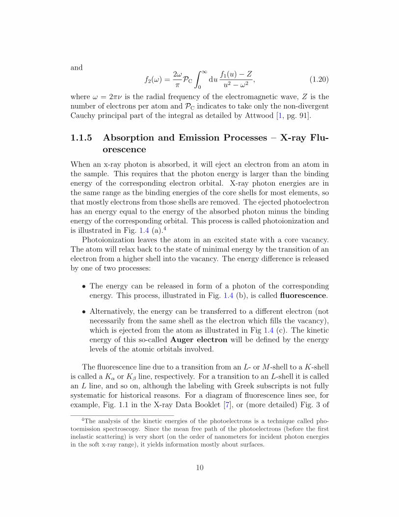
When an x-ray photon is absorbed, it will eject an electron from an atom inthe sample. This requires that the photon energy is larger than the bindingenergy of the corresponding electron orbital. X-ray photon energies are inthe same range as the binding energies of the core shells for most elements, sothat mostly electrons from those shells are removed. The ejected photoelectronhas an energy equal to the energy of the absorbed photon minus the bindingenergy of the corresponding orbital. This process is called photoionization andis illustrated in Fig. 1.4 (a).4
Photoionization leaves the atom in an excited state with a core vacancy.The atom will relax back to the state of minimal energy by the transition of anelectron from a higher shell into the vacancy. The energy difference is releasedby one of two processes:
• The energy can be released in form of a photon of the correspondingenergy. This process, illustrated in Fig. 1.4 (b), is called fluorescence.
• Alternatively, the energy can be transferred to a different electron (notnecessarily from the same shell as the electron which fills the vacancy),which is ejected from the atom as illustrated in Fig 1.4 (c). The kineticenergy of this so-called Auger electron will be defined by the energylevels of the atomic orbitals involved.
The fluorescence line due to a transition from an L- or M -shell to a K-shellis called a Kα or Kβ line, respectively. For a transition to an L-shell it is calledan L line, and so on, although the labeling with Greek subscripts is not fullysystematic for historical reasons. For a diagram of fluorescence lines see, forexample, Fig. 1.1 in the X-ray Data Booklet [7], or (more detailed) Fig. 3 of
4The analysis of the kinetic energies of the photoelectrons is a technique called pho-toemission spectroscopy. Since the mean free path of the photoelectrons (before the firstinelastic scattering) is very short (on the order of nanometers for incident photon energiesin the soft x-ray range), it yields information mostly about surfaces.
10

Nucleus
+Ze
Photon
(hν)
Photoelectron
(E = hν − EB)
K
M
L
(a)
Nucleus
+Ze
Fluorescent photon
hν = EL − EK
K
M
L
(b)
Nucleus
+Ze
Auger
electron
K
M
L
(c)
Figure 1.4: X-ray absorption and emission processes illustrated with a simpli-fied atomic model (after Attwood [1, Fig. 1.2]): (a) Photoionization throughan incident x-ray photon leaves the atom with a vacancy in a core shell. (b,c) An electron from a higher shells fills the vacancy. The energy difference is(b) released in form of a fluorescent photon, or (c) transferred to an Augerelectron which is also ejected from the atom.
11

L
M
K0.20
0 20 40 60 80
Z
0.001
0.01
0.10
1.00
Flu
ore
scence y
ield
Y
0.50
0.05
0.02
0.005
0.002
Figure 1.5: Fluorescence yields for the K, L and M shells as a function ofatomic number Z (data from Krause [10]).
Markowicz [3]. The wavelength of the fluorescent lines observed from a givenelement is well defined by the energy states of the atom and the selectionrules for allowed transitions (see Attwood [1] or any standard book on atomicphysics) and tabulations are available, such as in the aforementioned X-rayData Booklet. It can be measured with an energy-dispersive detector by thetechnique of x-ray fluorescence spectroscopy, where the elemental content of aspecimen is determined from the emission spectrum and the known emissionlines of all elements (see Sec. 1.3.4).5
The probability that the relaxation occurs through the process of fluores-cence (and not through Auger emission) is called the fluorescence yield. It islow for low-Z elements and high for high-Z elements as plotted in Fig. 1.5.This is the reason why fluorescence spectroscopy does not work well for lightelements such as carbon, nitrogen and oxygen (Z = 6, 7, and 8, respectively),which are among the main constituents of biological tissue.
Note that one can also use energetic electrons to eject core electrons froman atom. The incident electron will transfer part of its energy to the ejectedelectron and is scattered off at a new angle. The relaxation of the atom willagain occur through one of the two processes mentioned above. However,
5The technique of Auger electron spectroscopy studies the kinetic energy of Auger elec-trons for materials characterization. Due to the short range of Auger electrons in matter (onthe order of nanometers), it is mostly limited to surfaces, like photoemission spectroscopy.
12

when a material is bombarded with electrons of adequate energy, one will alsoobserve a continuous emission spectrum called “bremsstrahlung” (from theGerman word “bremsen”, for “to brake”) besides the characteristic fluorescentlines. This stems from the acceleration of the electrons in the Coulomb field ofthe specimen nuclei, whose magnitude depends on the (randomly distributed)distance of the electron trajectory from the nucleus. The bremsstrahlungcontinuum is cut off at a photon energy equal to the energy of the incidentelectrons.
X-ray emission induced by electron excitation is used mainly for two pur-poses:
• The study of fluorescence emission for elemental analysis and materi-als characterization, as described above for x-ray induced x-ray fluo-rescence. This method is more readily available than x-ray stimulatedfluorescence due to the widespread use of scanning electron microscopesequipped with an energy-dispersive x-ray detector, but is less sensitiveto small trace element amounts due to the aforementioned backgroundof bremsstrahlung.
• In x-ray tubes, for the purpose of generating x-rays. As mentioned above,the spectrum shows characteristic lines (depending on the anode mate-rial) on top of the continuous background. X-ray tubes are widely usedas x-ray sources for low-resolution imaging applications in the field ofmedicine and materials science, but have limited applicability in x-raymicroscopy due to the low brightness (see Sec. 1.2).
1.2 X-ray Microscopy
The field of x-ray microscopy using synchrotron radiation and zone plate opticswas established in the 1970s and 80s. The group of G. Schmahl at GottingenUniversity pioneered the full field microscope, while the group of J. Kirz atStony Brook developed the scanning microscope, both operating in the softx-ray energy range. Today, many synchrotrons around the world operate x-raymicroscopes from the soft to the hard x-ray range, with numerous applicationsin the fields of life, environmental, materials and other sciences. For a recentoverview, see, for example, Howells et al. [11].
1.2.1 Synchrotron Radiation Sources
Several dozens of synchrotron storage rings operate around the world andproduce bright x-ray beams for a wide range of applications. The experiments
13
described in this thesis were performed at two facilities:
• the National Synchrotron Light Source (NSLS)6 at Brookhaven NationalLaboratory (BNL), and
• the Advanced Photon Source (APS)7 at Argonne National Laboratory(ANL).
X-ray microscopes use radiation produced by either bending magnet sources(delivering high flux, measured in photons per second, per bandwidth, andper solid angle), or by undulator sources (optimized to deliver high brightness,which is flux per source area, and therefore more coherent radiation). Thecharacteristics of synchrotron radiation from these devices are described inthe books by Attwood [1] for the soft x-ray range and Mills (Ed.) [12] for thehard x-ray range, along with applications including x-ray microscopy.
1.2.2 Types of X-ray Microscopes
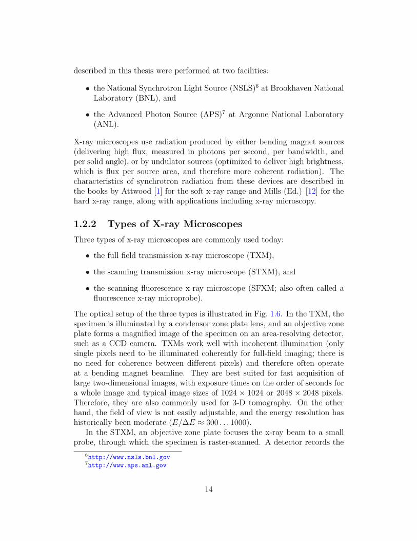
Three types of x-ray microscopes are commonly used today:
• the full field transmission x-ray microscope (TXM),
• the scanning transmission x-ray microscope (STXM), and
• the scanning fluorescence x-ray microscope (SFXM; also often called afluorescence x-ray microprobe).
The optical setup of the three types is illustrated in Fig. 1.6. In the TXM, thespecimen is illuminated by a condensor zone plate lens, and an objective zoneplate forms a magnified image of the specimen on an area-resolving detector,such as a CCD camera. TXMs work well with incoherent illumination (onlysingle pixels need to be illuminated coherently for full-field imaging; there isno need for coherence between different pixels) and therefore often operateat a bending magnet beamline. They are best suited for fast acquisition oflarge two-dimensional images, with exposure times on the order of seconds fora whole image and typical image sizes of 1024 × 1024 or 2048 × 2048 pixels.Therefore, they are also commonly used for 3-D tomography. On the otherhand, the field of view is not easily adjustable, and the energy resolution hashistorically been moderate (E/∆E ≈ 300 . . . 1000).
In the STXM, an objective zone plate focuses the x-ray beam to a smallprobe, through which the specimen is raster-scanned. A detector records the
6http://www.nsls.bnl.gov7http://www.aps.anl.gov
14

Undulatorsource with
monochromator
Bendingmagnetsource Condenser
zone plate
Objectivezoneplate
CCDcamera
Object
Object
Objectivezone plate
Detector
TXM: transmission x-ray microscope
STXM: scanning transmission x-ray microscope
Undulatorsource with
monochromator
Object
Objectivezone plate
Energy- dispersiveDetector
SFXM: scanning fluorescence x-ray microscope
Bright field cone
Figure 1.6: Types of x-ray microscopes: TXM, STXM and SFXM.
15

transmitted intensity for each scan position, so that the image is acquiredpixel by pixel. The direct beam incident on the detector (a projection ofthe aperture) is called the bright field cone as illustrated in Fig. 1.6. Fordiffraction-limited resolution, the zone plate has to be illuminated coherently,so that STXMs are best operated at undulator beamlines. Image acquisitionin a STXM is usually slower than in a TXM (minutes per image vs. seconds),but the STXM offers the following advantages:
• the field of view is easily variable from large overview scans to highresolution scans of small areas, only limited by the travel range andresolution of the scanning stage;
• the radiation dose imposed onto the specimen is lower than in a TXM forthe same signal to noise ratio, because the zone plate (whose efficiencyis on the order of only 10%) is located upstream of the sample in STXM;and
• it is well matched to the etendue (phase space acceptance) of a highenergy-resolution grating monochromator (E/∆E ≈ 3000 . . . 5000).
Therefore, the STXM is commonly used for spectromicroscopy (the combina-tion of spectroscopy and microscopy).
The SFXM is very similar to the STXM, but instead of the transmittedintensity, primarily fluorescent photons are recorded by an energy-dispersivedetector. This is used for elemental analysis of the specimen as described inSec. 1.1.5. Since the fluorescence detector is usually positioned at 90 degreesfrom the optical axis (the point of lowest background, while the fluorescentphotons are emitted uniformly in all directions), a transmission detector canbe installed additionally for a combined STXM / SFXM.
1.2.3 X-ray Optics – Fresnel Zone Plates
Lens-based microscopes use optics either to project a magnified image of thespecimen onto an imaging detector (in the case of a full-field microscope), orto form a small probe through which the specimen is raster-scanned (in thecase of a scanning microscope). Three types of x-ray optics are commonlyused:
• reflective (mirror) optics,
• refractive optics, and
• diffractive optics.
16
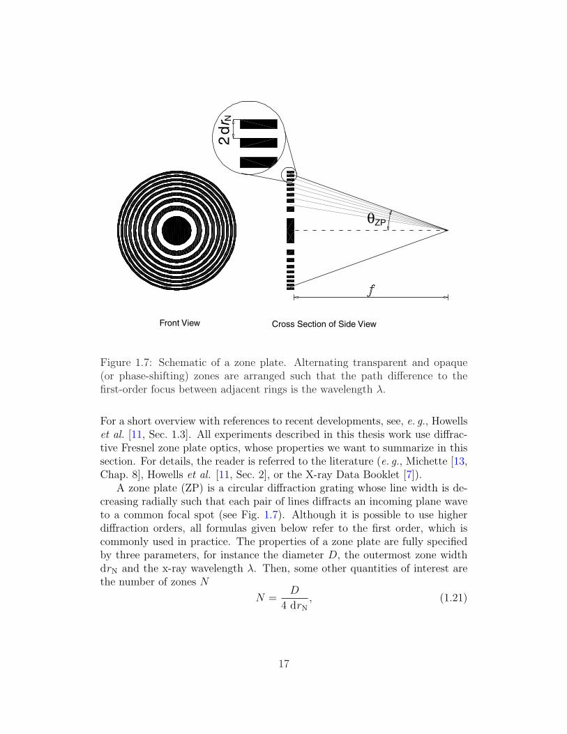
Cross Section of Side ViewFront View
θZP2
dr
N
Figure 1.7: Schematic of a zone plate. Alternating transparent and opaque(or phase-shifting) zones are arranged such that the path difference to thefirst-order focus between adjacent rings is the wavelength λ.
For a short overview with references to recent developments, see, e. g., Howellset al. [11, Sec. 1.3]. All experiments described in this thesis work use diffrac-tive Fresnel zone plate optics, whose properties we want to summarize in thissection. For details, the reader is referred to the literature (e. g., Michette [13,Chap. 8], Howells et al. [11, Sec. 2], or the X-ray Data Booklet [7]).
A zone plate (ZP) is a circular diffraction grating whose line width is de-creasing radially such that each pair of lines diffracts an incoming plane waveto a common focal spot (see Fig. 1.7). Although it is possible to use higherdiffraction orders, all formulas given below refer to the first order, which iscommonly used in practice. The properties of a zone plate are fully specifiedby three parameters, for instance the diameter D, the outermost zone widthdrN and the x-ray wavelength λ. Then, some other quantities of interest arethe number of zones N
N =D
4 drN
, (1.21)
17

the focal length f
f =D drN
λ, (1.22)
and the numerical aperture
NA = sin θZP =λ
2 drN
, (1.23)
where θZP is the half-opening angle (see Fig. 1.7).For uniform plane-wave illumination, the zone plate will form a diffraction
limited first-order focal spot with a transverse resolution (Rayleigh criterion;distance to the first minimum) of
δt = 1.22 drN (1.24)
as illustrated in Fig. 1.8. In fact, the wave field in the focal spot for plane-waveillumination is given by the Fourier transform of the pupil function (timesa phase factor, to be exact) [14, Sec. 5-2]. Note that the outermost zonewidth alone specifies the diffraction-limited transverse resolution, independentof the wavelength (this is true for drN À λ). The intensity distribution in thefocal plane is also called the Point Spread Function, or PSF. The longitudinalresolution (depth of field) δl is given by
δl = ± λ
2 (NA)2 = ±2 (drN)2
λ. (1.25)
Zone plates are chromatic optics (the focal length is inversely proportionalto the wavelength) and therefore require monochromatic illumination. Specifi-cally, the monochromaticity must be higher than the number of zones to avoidchromatic blurring:
λ
∆λ> N. (1.26)
To isolate the first-order focus from the direct beam (zero order) and higherdiffraction orders in a scanning microscope, a combination of a central stopand an order-sorting aperture is used (see Fig. 1.9).
To achieve a diffraction-limited focal spot in a scanning microscope, thezone plate has to be illuminated coherently, such as from a point source (whichis why scanning microscopes are best operated at an undulator source). Foran extended source the focal spot will be given by the convolution of thediffraction-limited focus with the geometrical image of the source. In practice,one can achieve diffraction-limited resolution if the geometrical image of the
18
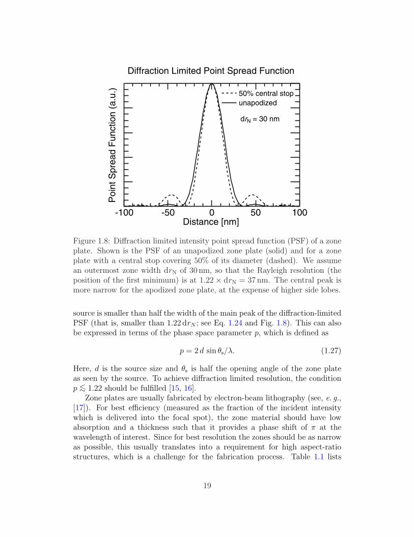
Po
int
Sp
rea
d F
un
ctio
n (
a.u
.)
Distance [nm]100500-50-100
Diffraction Limited Point Spread Function
unapodized
50% central stop
drN = 30 nm
Figure 1.8: Diffraction limited intensity point spread function (PSF) of a zoneplate. Shown is the PSF of an unapodized zone plate (solid) and for a zoneplate with a central stop covering 50% of its diameter (dashed). We assumean outermost zone width drN of 30 nm, so that the Rayleigh resolution (theposition of the first minimum) is at 1.22 × drN = 37 nm. The central peak ismore narrow for the apodized zone plate, at the expense of higher side lobes.
source is smaller than half the width of the main peak of the diffraction-limitedPSF (that is, smaller than 1.22 drN ; see Eq. 1.24 and Fig. 1.8). This can alsobe expressed in terms of the phase space parameter p, which is defined as
p = 2 d sin θs/λ. (1.27)
Here, d is the source size and θs is half the opening angle of the zone plateas seen by the source. To achieve diffraction limited resolution, the conditionp <∼ 1.22 should be fulfilled [15, 16].
Zone plates are usually fabricated by electron-beam lithography (see, e. g.,[17]). For best efficiency (measured as the fraction of the incident intensitywhich is delivered into the focal spot), the zone material should have lowabsorption and a thickness such that it provides a phase shift of π at thewavelength of interest. Since for best resolution the zones should be as narrowas possible, this usually translates into a requirement for high aspect-ratiostructures, which is a challenge for the fabrication process. Table 1.1 lists
19

Zone plate
OSA: ordersorting aperture
Incidentbeam
0 order
+1 order
+3 order
Focal
point
Finest zone of
width drN
Figure 1.9: The combination of a central stop on the zone plate and an order-sorting aperture (OSA) isolates the first-order focus in a scanning x-ray mi-croscope or microprobe. The required working distance between the OSA andthe focus (mostly an issue in the soft x-ray range) determines the minimumdiameter of the OSA and therefore the minimum size of the central stop. Thecentral stop should cover at most half the zone plate diameter not to degradethe quality of the focal spot too much (see Fig. 1.8).
typical zone plate parameters at x-ray energies used in this thesis work.
1.2.4 Description of Instruments
The experiments described in this thesis were performed at three differentscanning instruments, which are described here:
The Stony Brook STXM at the NSLS
The X-ray Microscopy Group at Stony Brook University has been developingand operating STXMs at beamline X1A at the National Synchrotron LightSource (NSLS) for many years. The beamline uses an undulator source and aspherical grating monochromator. It is designed to deliver a highly monochro-matic and coherent photon beam in the soft x-ray range (about 200 to 800 eV)to the end station; its present incarnation is described by Winn et al. [16].
The microscopes use zone plates with an outermost zone width of 30 to45 nm for high-resolution transmission imaging and near-edge spectroscopy ofspecimens mostly from the life, environmental and space sciences. Version 4
20
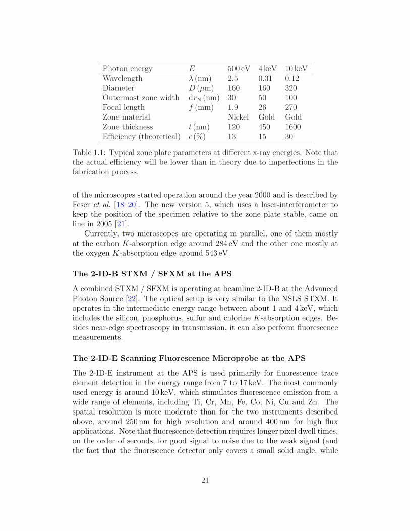
Photon energy E 500 eV 4 keV 10 keVWavelength λ (nm) 2.5 0.31 0.12Diameter D (µm) 160 160 320Outermost zone width drN (nm) 30 50 100Focal length f (mm) 1.9 26 270Zone material Nickel Gold GoldZone thickness t (nm) 120 450 1600Efficiency (theoretical) ε (%) 13 15 30
Table 1.1: Typical zone plate parameters at different x-ray energies. Note thatthe actual efficiency will be lower than in theory due to imperfections in thefabrication process.
of the microscopes started operation around the year 2000 and is described byFeser et al. [18–20]. The new version 5, which uses a laser-interferometer tokeep the position of the specimen relative to the zone plate stable, came online in 2005 [21].
Currently, two microscopes are operating in parallel, one of them mostlyat the carbon K-absorption edge around 284 eV and the other one mostly atthe oxygen K-absorption edge around 543 eV.
The 2-ID-B STXM / SFXM at the APS
A combined STXM / SFXM is operating at beamline 2-ID-B at the AdvancedPhoton Source [22]. The optical setup is very similar to the NSLS STXM. Itoperates in the intermediate energy range between about 1 and 4 keV, whichincludes the silicon, phosphorus, sulfur and chlorine K-absorption edges. Be-sides near-edge spectroscopy in transmission, it can also perform fluorescencemeasurements.
The 2-ID-E Scanning Fluorescence Microprobe at the APS
The 2-ID-E instrument at the APS is used primarily for fluorescence traceelement detection in the energy range from 7 to 17 keV. The most commonlyused energy is around 10 keV, which stimulates fluorescence emission from awide range of elements, including Ti, Cr, Mn, Fe, Co, Ni, Cu and Zn. Thespatial resolution is more moderate than for the two instruments describedabove, around 250 nm for high resolution and around 400 nm for high fluxapplications. Note that fluorescence detection requires longer pixel dwell times,on the order of seconds, for good signal to noise due to the weak signal (andthe fact that the fluorescence detector only covers a small solid angle, while
21

the fluorescent photons are emitted uniformly in all directions).2-ID-E uses an undulator and a single crystal (Si-111) monochromator in
a side-bounce geometry (the direct beam is used by a different instrument).
1.3 Image Contrast in Scanning X-ray Micros-
copy
The achievable contrast between different constituents of a specimen deter-mines the imaging mode which is most suitable in a given situation. Animportant point to consider is the damage done to the specimen by the effectsof radiation, in particular radiation-sensitive biological specimens.
1.3.1 Photon Statistics
Photons follow a Poisson distribution, which means that if we expect to countan average number of photons n in many measurements of the same type, theprobability of counting n photons in one particular measurement is
P (n, n) =nn
n!exp(−n). (1.28)
It can be shown that the standard deviation of a Poisson distribution is givenby√
n. In other words, if we expect to count n photons in a certain situation,the signal to noise ratio (SNR) is given by
SNR =Signal
Noise=
n√n
=√
n. (1.29)
This noise is intrinsic to the counting of photons and does not include othersources of noise, e. g., in the source or detector. A common criterion for thedetectability of a feature is the Rose criterion of SNR >∼ 5 [23].
The above means that in many cases, the signal to noise ratio can beimproved by using more photons. With a given instrument and therefore agiven photon flux, this can be achieved by using longer exposure times. Besidespractical issues (the desire for fast data taking), the limit to longer exposuresis often given by the radiation sensitivity of the specimen. In Chap. 3, we willcompare absorption and phase contrast with respect to their achievable SNRfor biological tissue at different x-ray energies.
For n >∼ 10, the Poisson distribution is approximated well by a Gaussian
22

distribution with the appropriate width, or
P (n, n) =1√2πn
exp
(−(n− n)2
2n
)(1.30)
with a truncation to P = 0 for n < 0.It should be noted that in practice, images will not only show photon noise,
but additional noise which stems from sources such as beam motion, vibrationof optical elements, or detector readout noise.
1.3.2 Absorption Contrast
This is the most “simple” and therefore most commonly used contrast modein x-ray microscopes. One just measures the intensity I transmitted throughthe specimen, either for the whole specimen at once with a spatially resolvingdetector in a full-field microscope, or on a pixel by pixel basis with a spatiallyintegrating detector in a scanning microscope (see Sec. 1.2.2). As described inSec. 1.1.3, one obtains a spatial map of the optical density of the specimen,which is the product of the absorption coefficient µ and the thickness t as afunction of sample coordinate r:
OD(r) = − lnI(r)
I0
= µ(r) · t(r). (1.31)
Here, I0 is the incident intensity, measured as the mean value in a specimen-free background region. Absorption contrast is thus due to variations in thethickness and the absorption coefficient across the specimen.
For thick specimens, where different materials could be “stacked” on topof each other in each image pixel, transmission contrast will yield a projectionthrough the specimen. If z is the direction of the optical axis, one will measure
OD(r) =
∫ t
0
µ(r, z) dz. (1.32)
Absorption contrast works particularly well for thick biological specimens(like whole cells) in their natural, wet environment in the so-called “waterwindow” as illustrated in Fig. 1.10.
The technique of x-ray absorption tomography reconstructs a three-dimen-sional image of the specimen from a series of 2-D projections at different angles.
23

0.1
1.0
10.0
Pe
ne
tra
tio
n d
ista
nce
(µ
m)
0 100 200 300 400Electron energy (keV)
0 500 1000 1500X-ray energy (eV)
(protein)
Electrons1/µ
(protein)C
arb
on
ed
ge
X-rays
λelastic (water)
1/µ (water)
(water)
Oxyg
en
ed
ge
λinelastic (protein)
Figure 1.10: Absorption length (penetration distance) of soft x-rays in pro-tein and water (from Kirz et al. [5]). As carbon is the main constituent ofbiological tissue, there is very good absorption contrast for such specimens intheir natural (wet) environment in the so-called “water window” between theK-absorption edges of carbon and oxygen at 284 eV and 543 eV, respectively.The penetration distance of high-energy electrons is given for comparison.
Element-specific Absorption Contrast
As shown above, the absorption coefficient as a function of energy shows theabsorption edges characteristic for the different elements. By taking imagesabove and below an absorption edge, one can obtain a quantitative map ofthat element’s mass [24].
XANES Contrast
X-ray absorption spectra show a fine structure in the vicinity of an absorptionedge, which is called X-ray Absorption Near-Edge Structure or XANES.8 Thisis due to the transition of inner shell electrons into incompletely occupied
8also called NEXAFS (Near-Edge X-ray Absorption Fine Structure)
24

molecular orbitals with an energy just below the continuum (instead of theelectron being fully ejected from the atom) as described, e. g., by Stohr [25].XANES spectra can yield detailed information on the binding state of the atomin a molecule (like, for example, carbon or oxygen in organic compounds).
X-ray microscopes with high energy resolution, like STXMs, can combineimaging and near-edge spectroscopy by acquiring a series of absorption imagesof the same sample region at closely spaced energies [26]. After aligning theimages, these so-called “stacks” give a near-edge absorption spectrum at everyimage pixel. They provide a wealth of information, and statistical methodsare useful in their interpretation [27].
1.3.3 Phase Contrast
Instead of mapping the specimen absorption, one can also measure the phaseshift
∆φ = δ(r) · k · t(r) (1.33)
imposed onto the incident x-ray wave (see Sec. 1.1.3) as a function of specimenposition r. For thick specimens, we measure
∆φ =
∫ t
0
δ(r, z) k dz (1.34)
in analogy to Sec. 1.3.2. As x-ray detectors are sensitive only to the intensityof the wave, and not to its phase, one must use some indirect method whichturns a phase difference into an intensity difference. Phase contrast is themajor topic of this thesis work, and a more detailed introduction is given inSec. 1.4.
1.3.4 Fluorescence Contrast
The emission of characteristic fluorescent photons (see Sec. 1.1.5) can be usedto obtain a map of the elemental content of the sample. In the SFXM, thespecimen is scanned through a small x-ray focus, and for each scan pixel thefluorescence spectrum is recorded with an energy-dispersive detector. Theincident energy determines the orbitals which can be excited and therefore therange of elements which can be detected. Fluorescence is very well suited forthe detection of trace elements (like transition metals) in biological, biomedicaland environmental samples. However, the method is usually not sensitive tolow-Z elements due to the low fluorescence yield (see Fig. 1.5) and thereforedoes not image the specimen ultrastructure, or tissue, well.
25

Figure 1.11: Example fluorescence spectrum. This is the spectrum of thespecimen shown in Fig. 3.10, integrated over the whole image. The Kα linesof selected elements are shown at the top. The broad peak around 10 keV,corresponding to the incident x-ray energy, is the elastic scattering signal.Spectrum generated with MAPS [28].
Fig. 1.11 shows an example fluorescence spectrum, showing the total ele-mental content (integrated over the whole image) of a phytoplankton cell (seeSec. 3.2.1). The spectrum of a single pixel would be much more noisy at atypical dwell time of one second.
1.3.5 Dark-Field Contrast
Small, strongly scattering structures like colloidal gold particles can be used,for instance, for immunolabeling of specific proteins in cells. Those structureswill scatter the incident radiation at large angles, outside the direct beam(bright field cone; see Fig. 1.6) in the STXM. If a stop is used to aperturethe direct beam from the detector, the labels will produce a strong scatteringsignal, which can map the labeled features with better signal to noise ratio(and therefore lower radiation dose) than in bright-field mode. This is calleddark-field microscopy [29–32].
26

In principle, a configured detector (see Sec. 1.4.2) can be used for thispurpose if it has dedicated segments covering the area outside the bright fieldcone, and if their sensitivity is matched to measure the weak scattering signal(which is orders of magnitude lower than the bright field signal).
1.4 Phase Contrast in X-ray Microscopy
In this section, we want to give a general introduction to the subject of phasecontrast. The remainder of this thesis will deal with details in instrumentationand data analysis, along with experimental results.
1.4.1 Motivation – Why Measure Phase Contrast
As we have seen in the previous section, transmission x-ray microscopes gener-ally image the spatial distribution of the refractive index of the specimen; thatis, either its imaginary part in absorption contrast, or its real part in phasecontrast. We have also established that absorption contrast is easy to measuredue to the intensity sensitivity of radiation detectors. By comparison, phasecontrast requires an indirect method which turns a phase difference into anintensity difference. Why is it still useful to measure phase?
In the Soft X-ray Range
We have described in Sec. 1.3.2 that the soft x-ray range is very suitableto absorption contrast measurements of biological specimens in their naturalenvironment. This is due to the strong difference in absorption between proteinand water in the “water window.” However, note that absorption also meansthat energy is deposited in the specimen, which can damage radiation-sensitivespecimens.
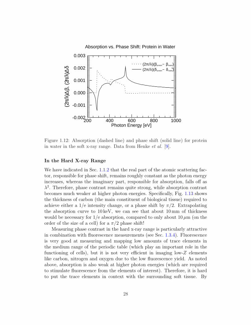
Fig. 1.12 shows the corresponding phase difference along with absorption.We can see that due to the coupling of f1 and f2 via the Kramers-Kronigrelations (see Sec. 1.1.4), each absorption edge is accompanied by a phase res-onance which is pronounced strongly at energies already below the absorptionedge. When imaging at such energies, phase provides strong contrast, whileabsorption and therefore radiation damage is low. It should even be possibleto perform near-edge spectroscopy in phase and relate it to known absorptionspectra with help of the Kramers-Kronig relations [33].
27
(2π/
λ)∆
β, (
2π/λ
)∆δ
0.003
0.002
0.001
0.000
-0.001
-0.002
Photon Energy [eV]1000800600400200
Absorption vs. Phase Shift: Protein in Water
(2π/λ)(δprotein− δwater)(2π/λ)(βprotein− βwater)
Figure 1.12: Absorption (dashed line) and phase shift (solid line) for proteinin water in the soft x-ray range. Data from Henke et al. [9].
In the Hard X-ray Range
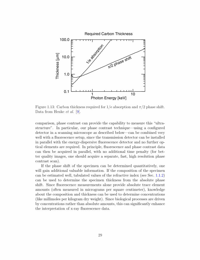
We have indicated in Sec. 1.1.2 that the real part of the atomic scattering fac-tor, responsible for phase shift, remains roughly constant as the photon energyincreases, whereas the imaginary part, responsible for absorption, falls off asλ2. Therefore, phase contrast remains quite strong, while absorption contrastbecomes much weaker at higher photon energies. Specifically, Fig. 1.13 showsthe thickness of carbon (the main constituent of biological tissue) required toachieve either a 1/e intensity change, or a phase shift by π/2. Extrapolatingthe absorption curve to 10 keV, we can see that about 10 mm of thicknesswould be necessary for 1/e absorption, compared to only about 10 µm (on theorder of the size of a cell) for a π/2 phase shift!
Measuring phase contrast in the hard x-ray range is particularly attractivein combination with fluorescence measurements (see Sec. 1.3.4). Fluorescenceis very good at measuring and mapping low amounts of trace elements inthe medium range of the periodic table (which play an important role in thefunctioning of cells), but it is not very efficient in imaging low-Z elementslike carbon, nitrogen and oxygen due to the low fluorescence yield. As notedabove, absorption is also weak at higher photon energies (which are requiredto stimulate fluorescence from the elements of interest). Therefore, it is hardto put the trace elements in context with the surrounding soft tissue. By
28
Th
ickn
ess [
µm
]
100.0
10.0
1.0
0.1
Photon Energy [keV]101
Required Carbon Thickness
1/e
abso
rptio
n
π/2 phase shift
Figure 1.13: Carbon thickness required for 1/e absorption and π/2 phase shift.Data from Henke et al. [9].
comparison, phase contrast can provide the capability to measure this “ultra-structure”. In particular, our phase contrast technique—using a configureddetector in a scanning microscope as described below—can be combined verywell with a fluorescence setup, since the transmission detector can be installedin parallel with the energy-dispersive fluorescence detector and no further op-tical elements are required. In principle, fluorescence and phase contrast datacan then be acquired in parallel, with no additional time penalty (for bet-ter quality images, one should acquire a separate, fast, high resolution phasecontrast scan).
If the phase shift of the specimen can be determined quantitatively, onewill gain additional valuable information. If the composition of the specimencan be estimated well, tabulated values of the refractive index (see Sec. 1.1.2)can be used to determine the specimen thickness from the absolute phaseshift. Since fluorescence measurements alone provide absolute trace elementamounts (often measured in micrograms per square centimeter), knowledgeabout the composition and thickness can be used to determine concentrations(like millimoles per kilogram dry weight). Since biological processes are drivenby concentrations rather than absolute amounts, this can significantly enhancethe interpretation of x-ray fluorescence data.
29
optic
split detector
object withphase gradient
Figure 1.14: Differential phase contrast principle. Phase gradients in the spec-imen deflect the beam sideways, like a prism for visible light. The resultingshift of the “center of mass” of the beam can be measured, for example, witha detector which is split across the direction of the shift.
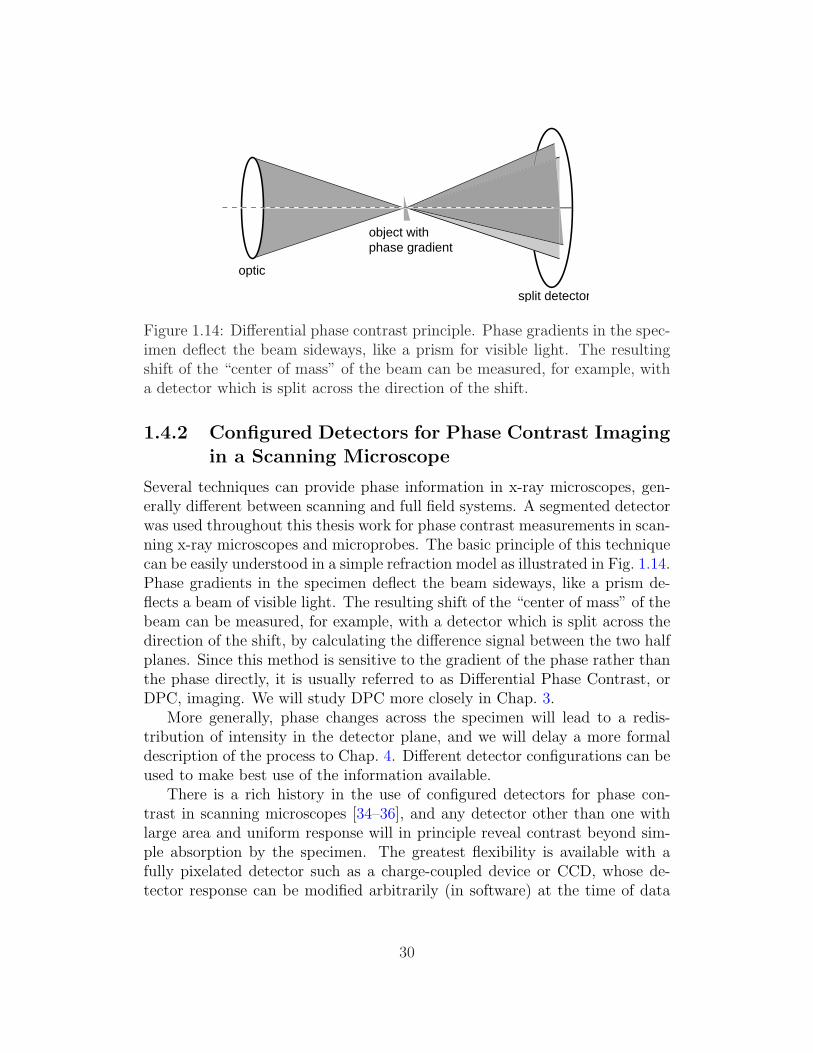
1.4.2 Configured Detectors for Phase Contrast Imagingin a Scanning Microscope
Several techniques can provide phase information in x-ray microscopes, gen-erally different between scanning and full field systems. A segmented detectorwas used throughout this thesis work for phase contrast measurements in scan-ning x-ray microscopes and microprobes. The basic principle of this techniquecan be easily understood in a simple refraction model as illustrated in Fig. 1.14.Phase gradients in the specimen deflect the beam sideways, like a prism de-flects a beam of visible light. The resulting shift of the “center of mass” of thebeam can be measured, for example, with a detector which is split across thedirection of the shift, by calculating the difference signal between the two halfplanes. Since this method is sensitive to the gradient of the phase rather thanthe phase directly, it is usually referred to as Differential Phase Contrast, orDPC, imaging. We will study DPC more closely in Chap. 3.
More generally, phase changes across the specimen will lead to a redis-tribution of intensity in the detector plane, and we will delay a more formaldescription of the process to Chap. 4. Different detector configurations can beused to make best use of the information available.
There is a rich history in the use of configured detectors for phase con-trast in scanning microscopes [34–36], and any detector other than one withlarge area and uniform response will in principle reveal contrast beyond sim-ple absorption by the specimen. The greatest flexibility is available with afully pixelated detector such as a charge-coupled device or CCD, whose de-tector response can be modified arbitrarily (in software) at the time of data
30

analysis. For instance, one can collect the full microdiffraction pattern ateach scan position, and indeed the reconstruction of specimen amplitude andphase by means of Wigner-distribution deconvolution [37] has been demon-strated in STXM [38]. Several STXMs have been equipped with CCDs fordemonstration experiments or as standard detectors [39–44]. However, theseapproaches still have complications of readout time and storage (a CCD framehas to be acquired and stored for each scan pixel) as well as signal to noise(the transmitted signal is divided among 103 to 106 CCD pixels, so the noiserequirements per pixel become quite demanding). Fortunately, much simplerdetector configurations can reveal the phase information desired. With a first-moment detector, the signal will be proportional to the phase gradient of thespecimen even for strong phase objects [45, 46]; such a detector can again berealized with a pixelated detector, or even with a wedge absorber [47].
A detector with a small number of separate segments offers a large de-gree of flexibility while increasing the readout and storage requirements onlymoderately. Such a detector has been described by Feser et al. for soft x-rays[20, 48], and Chap. 2 of this thesis describes the further development of thatdetector for higher x-ray energies at third generation synchrotron sources. Dif-ference images between opposing segments exhibit differential phase contrastas described above (also see [34, 36, 46, 49]). Clearly, the sum of all signalswill deliver the same absorption contrast image which would be obtained witha simple large-area detector. All those signals are available in parallel and inreal-time (while scanning), without complicated signal processing. However,DPC images can be hard to interpret (see Chap. 3) due to the differentialnature and the directional dependence of the signal. Therefore, in Chap. 4we discuss a Fourier filtering technique for the quantitative reconstruction ofspecimen amplitude and phase from segmented detector data.
1.4.3 Other Phase Contrast Techniques
The first phase contrast measurements in lens-based x-ray microscopes weredone by Schmahl et al. [50], using the Zernike technique [51] in a full-field mi-croscope. More methods, including the Nomarski, interferometric, holographicand propagation-based methods, are described in a recent review by Momose[52]. In scanning systems, there have been demonstrations with configureddetectors as described above [29, 53], a wavefront profiler in combination witha slit detector [54–56], aperture alignment [57], and the use of offset zone platedoublets [58].
31

Chapter 2
A Segmented Silicon Detectorfor Hard X-ray Microprobes
32

We have seen in the previous chapter that a segmented transmission detectorcan be used for phase contrast measurements in a scanning microscope ormicroprobe. Such a detector has been developed as part of a previous Ph.D.project for soft x-ray applications at the NSLS [20, 48, 59]. Here we describe asecond version of the detector more suitable for use in hard x-ray microprobesas they exist at the Advanced Photon Source (APS) at Argonne NationalLaboratory. It has again been developed in collaboration with Dr. Pavel Rehakfrom the Instrumentation Division at Brookhaven National Laboratory. Fromnow on, we will refer to the two different versions as the NSLS detector andthe APS detector, or the soft and the hard x-ray detector.
2.1 Requirements for a Transmission Detector
in Scanning X-ray Microscopes and Mi-
croprobes
Feser [20, Chap. 3.1] provides an excellent description of the requirements fora transmission detector in a scanning x-ray microscope or microprobe, whichwe want to summarize here:
Energy resolution is not required since the energy of the incoming beam ismonochromatic and usually known.
Spatial resolution is not required for simple absorption imaging, but pro-vides a means for phase contrast imaging (see Sec. 1.4.2). Amongthe most common spatially resolving x-ray detectors are CCD cameras(Charge-Coupled Devices). In the soft x-ray range, these are usuallyused in direct detection mode, while with hard x-rays a scintillator andimaging or fiber optics coupling scheme is used. Full 2-D detectors wouldbe ideal for STXM in terms of the information collected. However, thefollowing limitations exist:
1. Due to the serial readout of the pixels in a CCD, the readout timeis usually too long compared to the pixel dwell times used in STXM(also see below).
2. Such a detector would produce a huge amount of data (a full CCDframe would be read out for each scan pixel), which is difficult tohandle, store and process even with today’s powerful computers.
3. Since the photons collected are distributed over a large number ofdetector pixels, the statistical significance of a single pixel is limited.
33

Although the second and third of these limitations can be overcomeby rebinning the data (in which case the detector configuration can bechosen with a large degree of freedom at the time of rebinning), the firstone makes the use of current CCD detectors impractical in a scanningmicroscope or microprobe if fast scans on the order of millisecond pixeldwell times are desired. Despite these challenges, several STXMs havebeen equipped with CCDs for demonstration experiments or as standarddetectors [39–44].
Detectors with a small number of separate segments offer a large degreeof flexibility for different imaging modes, while increasing the readoutand storage requirements only moderately. Unfortunately, they are notcommercially available due to the limited range of applications. In thischapter, we present a custom-made segmented detector tailored to usein scanning x-ray microscopes and microprobes at intermediate and highphoton energies at third-generation synchrotron sources.
Currently, several groups around the world are working on the develop-ment of pixelated x-ray detectors with fast parallel readout (see, e. g.,[60–63]). If such detectors become more widely available in the futureand achieve sub-millisecond readout times, they might prove ideal forSTXM applications and make the development of specialized segmenteddetectors unnecessary.
Time Resolution and Detector Speed: In STXM, one is interested in thetotal number of photons detected within one scan pixel. Time resolutionwithin one scan pixel is therefore not required. However, there are twoaspects to detector speed which play a role:
• The detector should be capable of measuring high photon flux,which at modern synchrotron sources can be 1010 per second ormore. This is a problem for counting detectors (such as gas-filledproportional counters or avalanche photodiodes), whose dead timeis dictated by space-charge limits, or by other factors such as de-tector circuitry. Consequently, such detectors usually run into non-linearities above photon rates of a few tens of MHz or earlier. Notethat the time structure of synchrotron storage rings can aggravatethis effect as noted by Feser [20, Sec. 3.2]. Integrating detectors arenot affected by this problem.
• An integrating detector has to be read out rapidly enough not toaffect the usable pixel dwell times too much. If the detector is“dead” during readout, like a CCD without frame storage, the total
34
readout time should be significantly smaller than the pixel dwelltime. If the detector can perform a new integration during readoutof the previous signal, the readout time may approach the pixeldwell time, but not go beyond. This factor limits the usefulness ofCCD detectors in STXM if millisecond dwell times are desired, asdescribed above.
Detective Quantum Efficiency (DQE) is defined as
DQE =
(SNRout
SNRin
)2
, (2.1)
where SNRout, in are the signal to noise ratios of the detector output andinput signal, respectively. It is therefore a good measure of the perfor-mance of an entire detector system and depends of course on the perfor-mance of the components (such as the quantum efficiency of the siliconchip, and the readout noise of the electronics in the case of the detectordescribed in this chapter). A discussion of the relative performance oftypical integrating and counting detectors at low and high count rates isgiven, for example, by Feser [20, Sec. 3.1.4].
Linearity is essential for quantitative experiments. Counting detectors usu-ally suffer from nonlinearities when the mean time between incident pho-tons becomes comparable to the detector dead time. Integrating detec-tors, like the one described in this chapter, do not suffer from this effectand are linear up to the saturation level.
The Dynamic Range describes the range of signal levels in which a detectorcan be used. The relative dynamic range is given by the ratio of themaximum signal level and the noise level, and is more or less constantfor the detector system described in this chapter. The absolute rangecan be adjusted within limits to match the requirements of a specificbeamline.
Practical issues: As noted by Feser, ruggedness, ease of use and reliabilityare often more important than a further improvement in (theoretical)performance.
35

2.2 Review: The Existing Segmented Silicon
Detector
Here we want to briefly summarize the features of the previously developedsoft x-ray detector, which has been described in detail elsewhere [20, 48, 59].Some of the features will be reviewed later in more detail if they apply to thenew version as well.
The detector consists of a segmented silicon chip and charge integratingelectronics. It is optimized for soft x-ray applications in the energy rangebetween 200 and 800 eV, signal rates on the order of 106 photons per secondincident on the specimen and pixel dwell times of a few milliseconds.
The silicon chips have been developed in collaboration with, and fabricatedby, Lothar Struder, Peter Holl and others at the Max Planck SemiconductorLaboratory1 in Munich, Germany. Eight segments have been implanted aspatterned p/n-junctions into 300 µm thick n-type silicon (9 and 10 segmentsin later designs; see Sec. 2.4.3). It has excellent quantum efficiency from 250 eVto 10 keV (> 80%; see Sec 2.4.2).
The electronics consist of 10 channels for parallel readout of up to 10 detec-tor segments; they integrate the total charge produced in each segment duringone integration cycle. The integration cycle is controlled externally to matchthe pixel dwell time of the STXM. The readout noise is about 500 electrons,corresponding to about five photons per channel at 360 eV photon energy. Anabsolute calibration in terms of photons per second is available.
For preliminary experiments at higher photon energies, we have used amodified version of this detector with the feedback capacitance increased byabout a factor of 10. This was adequate to use at beamline 2-ID-B (seeSec. 1.2.4) in low-flux experiments. At 2-ID-E we have used this detectorwith an aluminum absorber (initially a piece of a coke can!), which absorbedmore than 99% of the radiation. Although we have obtained good differentialphase contrast images with that detector (see Sec. 3.2), for permanent useand better quantitative measurements it was desirable to have new detectorelectronics optimized for the signal levels of each instrument.
2.3 Limitations of the Existing Detector for
Hard X-ray Microscopy
To understand the modifications required to use the detector at hard x-raybeamlines at the APS, we compare the illumination conditions at different
1http://www.hll.mpg.de/
36

Beamline Primary appli-cation
Φ E I tdwell
NSLS X1A STXM 106/ s 200–800 eV 1–20 pA 1–10 msAPS 2-ID-B STXM / Fluo-
rescence108/ s 1–4 keV 1–100 nA sub-ms – sec
APS 2-ID-E Fluorescence 109/ s 7–17 keV 0.1–1µA sub-ms – secNanoprobe Fluorescence 1010/ s 3 (–30)a keV 0.5–5µA sub-ms – sec
aThe energy range for the segmented silicon detector is restricted to <∼ 15 keV due tothe limited quantum efficiency of the chip; see Sec. 2.4.2.
Table 2.1: Illumination conditions at NSLS and APS instruments.
instruments. They are determined by
• the typical photon flux Φ incident on the illuminated segments (measuredin photons per second);
• the photon energy E (as dictated by the primary contrast mechanism tobe used); and
• the desired pixel dwell time tdwell.
Considering that 3.62 eV of energy deposited in the silicon chip creates oneelectron-hole pair at room temperature (see, e. g., [64, Table 11-1]), one cancalculate the signal current created in one particular detector segment as
I = ε · e · Φ · E
3.62 eV, (2.2)
where ε is the photon detection efficiency of the chip (see Sec. 2.4.2; > 80%in the photon energy range of interest) and e is the charge of the electron(1.602× 10⁻¹⁹ C). The total amount of charge to be collected within one pixeldwell time is given by
Q = I · tdwell. (2.3)
Table 2.1 summarizes those quantities for the X1A STXM at the NSLS [65],for which the first generation of the detector was designed, and three instru-ments at the APS (also see Sec. 1.2.4): the 2-ID-B intermediate-energy STXM/ SFXM [22], the 2-ID-E fluorescence microprobe and the new Nanoprobe in-strument under development [66]. As can be seen, the signal currents areseveral orders of magnitude higher at the APS instruments compared to theNSLS STXM, so that the charge to be collected even during short (millisecond)dwell times scales by the same amount.
37

An additional complication is given by the fact that at fluorescence micro-probes, the dwell times can vary strongly from milliseconds for fast overviewscans up to several seconds per pixel for the actual fluorescence trace elementmapping. A dynamic range of about 5000 (which is a typical value to achievefor an electronic circuit of that kind) is already required to cover the signalrate for constant pixel dwell times due to variations in the incident photonflux. It would be very difficult to increase the dynamic range further to alsoaccommodate integration time variations over several orders of magnitude.Therefore, we have developed a concept to decouple detector integration andpixel dwell times (see Sec. 2.5.4).
In the NSLS detector, the signal currents could be as low as the leakage(dark) current of the chip, and the feedback capacitance which integrates thecharge is on the order of the inherent capacitances of the components and theprinted-circuit board. This is very different in the case of the APS detector,which therefore required a different design of the electronics.
2.4 Segmented Silicon Chip
The silicon detector chip could be used without modification at both the NSLSand the APS. However, its response at higher energies leads to some differencesin its properties and behavior, which will be described below.
2.4.1 Photodiode Principle
Photodiodes consist of a p/n-junction and are commonly used as detectors ofionizing radiation. Photons of sufficient energy can be absorbed in the diodeand create charge carriers (electron-hole pairs). If the absorption occurs inthe depletion region of the junction, the charge carriers are swept away by thebuilt-in field and produce a photocurrent; while the current measures photonrate, the total charge produced measures net absorbed radiation. A reversebias voltage can be applied to increase the width of the depletion region andimprove charge collection efficiency.
It should also be noted that minority charge carriers produce a leakage cur-rent (also called dark current), which adds to the photocurrent and is thereforeundesirable (see Sec. 2.4.4 and 2.4.6). For more details about photodiodes, thereader is referred to Knoll [64, Chap. 11] or any standard book on semicon-ductor physics.
38

Rela
tive Inte
nsity
1.0
0.8
0.6
0.4
0.2
0.0
Penetration Distance [µm]5004003002001000
X-ray Absorption in Silicon
20 keV
15 keV12 keV10 keV
8 keV
5 k
eV
2 keV
Figure 2.1: X-ray absorption in silicon for various photon energies. Data fromHenke et al. [9].
2.4.2 X-ray Absorption in Silicon and Chip QuantumEfficiency
The quantum efficiency describes the fraction of photons which are absorbedin the sensitive (depleted) region of the photodiode and therefore contribute tothe photocurrent. If the chip is fully depleted with a sufficiently large reversebias voltage, and used at photon energies above 1 keV (where absorption in thesilicon dioxide layer on the surface is negligible), the efficiency can be calculatedto good approximation from the thickness of the chip and the tabulated valuesof the x-ray absorption length in silicon [9]. At higher photon energies, thethickness is the limiting factor of detection efficiency, because a fraction of thephotons is passing unimpeded through the chip.
Fig. 2.1 shows the exponential decline of intensity as photons penetrateinto the silicon chip. A 300 µm thick chip is almost 100% efficient at photonenergies up to 8 keV. At 15 keV, the efficiency drops to about 45%, and evenan increased thickness of 500 µm improves it only moderately. Beyond 15, orat most 20 keV, silicon is not very useful any more as a direct x-ray detectormaterial.
As can be seen from Fig. 2.2, germanium would be a more suitable materialat higher photon energies because the absorption length is more than an orderof magnitude shorter than in silicon above 10 keV. While the fabrication ofsilicon radiation detectors has profited tremendously from the expertise of
39

Ab
so
rptio
n le
ng
th [
µm
]
104
103
102
101
100
10-1
10-2
Photon Energy [keV]101
GermaniumSilic
on
X-ray Absorption Length
Figure 2.2: X-ray absorption length in silicon and germanium. Data fromHenke et al. [9].
the microelectronics industry, further research efforts are required to developsimilar fabrication technologies for high quality germanium detectors.2
At soft x-ray energies, absorption effects in the silicon dioxide layer on thechip surface (before the photons can reach the depletion region) degrade thequantum efficiency slightly as shown in Fig. 2.3. Still, for photon energies usedat the NSLS STXM (starting at 280 eV), the quantum efficiency is above 80%.The plot also shows the decline of the quantum efficiency beyond 8 keV dueto the limited thickness as described above.
2.4.3 Chip Design and Production
The chips are fabricated out of 300 to 450 µm thick n-type high resistivity(5 kΩ · cm) silicon, commonly used for the detection of charged particles andx-rays. The back side has a continuous n+-implant which serves as an ohmiccontact to apply a positive bias voltage. The front side has all segmentsimplanted with p-type material (boron) to form rectifying p/n-junctions. Toachieve high quantum efficiency at low photon energies, the implant has to bevery shallow due to the short x-ray absorption length in silicon (see Sec. 2.4.2).At high photon energies, the quantum efficiency of the chip is limited by the
2See, e. g., Sec. 5.2 in the NSLS Five Year Plan at http://www.nsls.bnl.gov/newsroom/publications/manuals/5YearPlan.pdf.
40
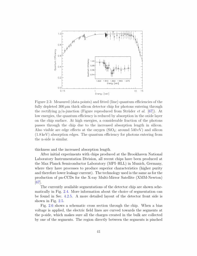
Figure 2.3: Measured (data points) and fitted (line) quantum efficiencies of thefully depleted 300 µm thick silicon detector chip for photons entering throughthe rectifying p/n-junction (Figure reproduced from Struder et al. [67]). Atlow energies, the quantum efficiency is reduced by absorption in the oxide layeron the chip surface. At high energies, a considerable fraction of the photonspasses through the chip due to the increased absorption length in silicon.Also visible are edge effects at the oxygen (SiO2; around 540 eV) and silicon(1.8 keV) absorption edges. The quantum efficiency for photons entering fromthe n-side is similar.
thickness and the increased absorption length.After initial experiments with chips produced at the Brookhaven National
Laboratory Instrumentation Division, all recent chips have been produced atthe Max Planck Semiconductor Laboratory (MPI–HLL) in Munich, Germany,where they have processes to produce superior characteristics (higher purityand therefore lower leakage current). The technology used is the same as for theproduction of pn-CCDs for the X-ray Multi-Mirror Satellite (XMM-Newton)[67].
The currently available segmentations of the detector chip are shown sche-matically in Fig. 2.4. More information about the choice of segmentation canbe found in Sec. 4.2.5. A more detailed layout of the detector front side isshown in Fig. 2.5.
Fig. 2.6 shows a schematic cross section through the chip. When a biasvoltage is applied, the electric field lines are curved towards the segments atthe p-side, which makes sure all the charges created in the bulk are collectedby one of the segments. The region directly between the segments is pinched
41
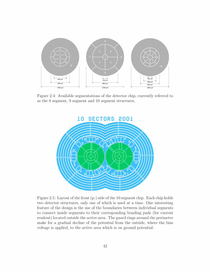
400 µm
600 µm
1200 µm
1
2
3
4
5 6
7
8
800 µm
1200 µm
150 µm
1
23
4 5
6
7
8
9
400 µm
600 µm
1200 µm
150 µm
1
23
4 5
6
7
8
9
10
Figure 2.4: Available segmentations of the detector chip, currently referred toas the 8 segment, 9 segment and 10 segment structures.
Figure 2.5: Layout of the front (p-) side of the 10 segment chip. Each chip holdstwo detector structures, only one of which is used at a time. One interestingfeature of the design is the use of the boundaries between individual segmentsto connect inside segments to their corresponding bonding pads (for currentreadout) located outside the active area. The guard rings around the perimetermake for a gradual decline of the potential from the outside, where the biasvoltage is applied, to the active area which is on ground potential.
42
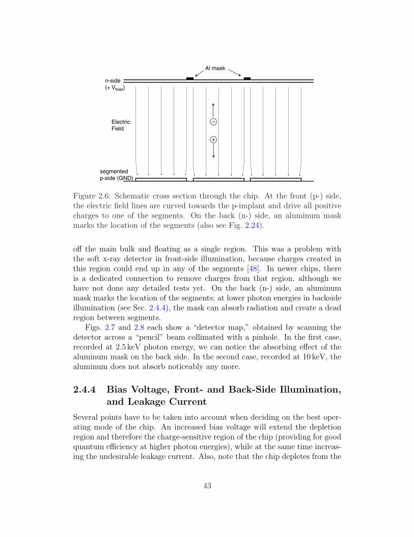
ElectricField
segmented p-side (GND)
n-side (+ Vbias)
Al mask
−
+
Figure 2.6: Schematic cross section through the chip. At the front (p-) side,the electric field lines are curved towards the p-implant and drive all positivecharges to one of the segments. On the back (n-) side, an aluminum maskmarks the location of the segments (also see Fig. 2.24).
off the main bulk and floating as a single region. This was a problem withthe soft x-ray detector in front-side illumination, because charges created inthis region could end up in any of the segments [48]. In newer chips, thereis a dedicated connection to remove charges from that region, although wehave not done any detailed tests yet. On the back (n-) side, an aluminummask marks the location of the segments; at lower photon energies in backsideillumination (see Sec. 2.4.4), the mask can absorb radiation and create a deadregion between segments.
Figs. 2.7 and 2.8 each show a “detector map,” obtained by scanning thedetector across a “pencil” beam collimated with a pinhole. In the first case,recorded at 2.5 keV photon energy, we can notice the absorbing effect of thealuminum mask on the back side. In the second case, recorded at 10 keV, thealuminum does not absorb noticeably any more.
2.4.4 Bias Voltage, Front- and Back-Side Illumination,and Leakage Current
Several points have to be taken into account when deciding on the best oper-ating mode of the chip. An increased bias voltage will extend the depletionregion and therefore the charge-sensitive region of the chip (providing for goodquantum efficiency at higher photon energies), while at the same time increas-ing the undesirable leakage current. Also, note that the chip depletes from the
43
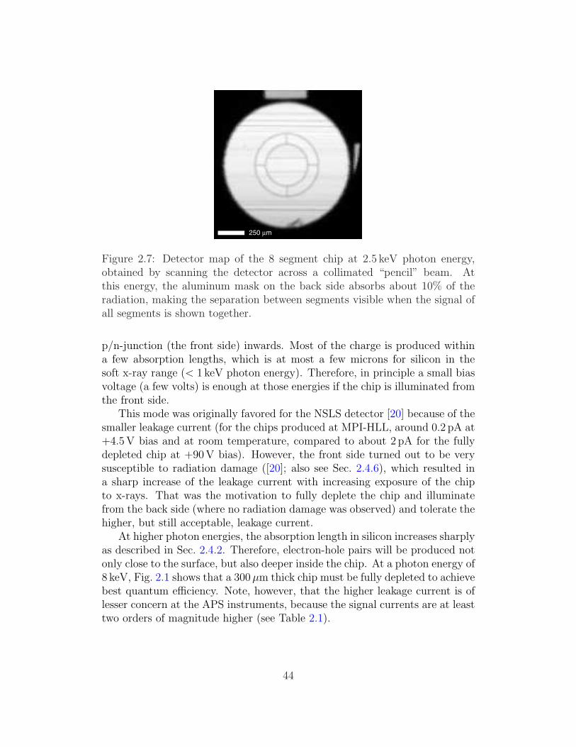
250 µm
Figure 2.7: Detector map of the 8 segment chip at 2.5 keV photon energy,obtained by scanning the detector across a collimated “pencil” beam. Atthis energy, the aluminum mask on the back side absorbs about 10% of theradiation, making the separation between segments visible when the signal ofall segments is shown together.
p/n-junction (the front side) inwards. Most of the charge is produced withina few absorption lengths, which is at most a few microns for silicon in thesoft x-ray range (< 1 keV photon energy). Therefore, in principle a small biasvoltage (a few volts) is enough at those energies if the chip is illuminated fromthe front side.
This mode was originally favored for the NSLS detector [20] because of thesmaller leakage current (for the chips produced at MPI-HLL, around 0.2 pA at+4.5 V bias and at room temperature, compared to about 2 pA for the fullydepleted chip at +90 V bias). However, the front side turned out to be verysusceptible to radiation damage ([20]; also see Sec. 2.4.6), which resulted ina sharp increase of the leakage current with increasing exposure of the chipto x-rays. That was the motivation to fully deplete the chip and illuminatefrom the back side (where no radiation damage was observed) and tolerate thehigher, but still acceptable, leakage current.
At higher photon energies, the absorption length in silicon increases sharplyas described in Sec. 2.4.2. Therefore, electron-hole pairs will be produced notonly close to the surface, but also deeper inside the chip. At a photon energy of8 keV, Fig. 2.1 shows that a 300 µm thick chip must be fully depleted to achievebest quantum efficiency. Note, however, that the higher leakage current is oflesser concern at the APS instruments, because the signal currents are at leasttwo orders of magnitude higher (see Table 2.1).
44

250 µm
1
987
654
32
Figure 2.8: Detector map of the 9 segment chip at 10 keV photon energy,obtained by scanning the detector across a collimated “pencil” beam. At thisenergy, the aluminum mask on the back side does not absorb noticeably, sothat one could not distinguish individual segments if all of them were displayedtogether. The bonding pads used for connecting the detector segments to thereadout electronics (see Fig. 2.5) are also visible. The location of individualnumbered segments (compare Fig. 2.4) is determined by the orientation of thechip when mounted in the microscope, and by the scan direction.
45

2.4.5 Effects of Insufficient Bias Voltage
The first batches of detector chips produced at MPI–HLL were 300 µm thickand were found to require about 90 V bias for full depletion. Later, chips werefabricated on thicker (450 µm) silicon wafers, which require a higher bias volt-age. Since the original electronics were designed for up to 90 V bias, and sincehigher voltages generally require more careful design and handling, we have an-alyzed the effects of a lower bias voltage on the charge collection performanceof the chips.
Electric Potential in the Chip
The electric potential V in the chip can be calculated from the solution of thePoisson equation:
∆V =
0 in the undepleted region, and
− ρ
ε0εr
in the depleted region, (2.4)
where ∆ = ∂2
∂x2 + ∂2
∂y2 + ∂2
∂z2 is the Laplace operator, ρ = ND · e is the charge
density (depending on the doping density ND ≈ 1012 cm−3 and the charge ofthe electron e = 1.6×10⁻¹⁹ C), and ε0εr = 663 e/( µm ·V) in silicon. Note thatthe charge density is zero in the undepleted region!
We can easily calculate a simplified one-dimensional solution by integratingalong the z-axis (perpendicular to the chip surface). Assume that the n-sideis located at z = 0, and the segmented p-side is at z = z0 as illustrated inFig. 2.9. We call zu the width of the undepleted region, so that zd = z0 − zu
is the width of the depletion layer. We also define
α = ρ/(ε0εr). (2.5)
As mentioned before, the chip depletes from p/n-junction (p-side) inwards.Then, under the condition that the electric field E = ∂V/∂z, and the potentialV itself, are continuous at the boundary between depleted and undepletedregion, we find from Eq. 2.4 that
∂V (z)
∂z=
A for 0 ≤ z < zu
−α(z − zu) + A for zu ≤ z ≤ z0(2.6)
46

0 100 200 300 400Profile through chip (µm)
0
50
100
150
Pote
ntial (V
)
n-side
positive bias applied segmented
p-side
+
+
+
x, y
x, y
Segm
ent 1
Segm
ent 2
120 V bias
90 V bias
60 V biasregion of
flat potential
(undepleted)
z
zu (60 V) zd (60 V)
Figure 2.9: Electric potential in the detector chip. In this plot, a bias of120 V fully depletes the 400 µm thick chip. Positive charges (holes) which areproduced in the chip can “roll down” the potential curve to the p-side, wherethey are collected in the segments. In the case of insufficient bias voltage (90 V,60 V), the potential has a flat region towards the n-side (no electric field).Holes which are produced in this region undergo a “random walk”. Even ifthey reach the region of declining potential within their lifetime (before theyrecombine with electrons), they might have traveled in the transverse (x, y)direction so that they lost their position information and are collected by thewrong segment.
47

and
V (z) =
Az + B for 0 ≤ z < zu
−α2(z − zu)
2 + A(z − zu) + B for zu ≤ z ≤ z0(2.7)
where A and B are integration constants. If a positive bias voltage Vbias isapplied at the n-side and the p-side is held on ground (V = 0), A, B and zu
are determined by the following conditions:
1. V = Vbias at the n-side (z = 0),
2. V = 0 at the p-side (z = z0), and
3.∂V
∂z= 0 defines the edge of the depletion layer (z = zu).
These conditions yield the following:
1. A = 0,
2. B = Vbias,
3. zd =
√2Vbias
α
To summarize, the potential in the chip is given by
V (z) =
Vbias for 0 ≤ z < zu
Vbias − α2(z − zu)
2 for zu ≤ z ≤ z0(2.8)
and
zu = z0 − zd = z0 −√
2 Vbias
α. (2.9)
Now let us assume ND = 1012 cm−3 = 1 µm−3. Then, α = 1.5×10⁻³ V/ µm2. Ifwe have a z0 = 400 µm thick chip, Eq. 2.9 yields that Vbias = 120 V is requiredfor full depletion (zu = 0). We also see (Fig. 2.9) that if we apply only 90 or60 V bias, a thickness of 55 or 118 µm is left undepleted, respectively.
Determination of Required Bias Voltage
It should be noted that the doping density is difficult to control in the fabri-cation process of the chips, so that the required depletion voltage should bemeasured for each wafer individually. This is usually done by measuring the
48
capacitance of the wafer (or chip) as a function of bias voltage. The chip canbe considered to be a parallel-plate capacitor, whose capacitance is given by
Cchip = ε0εrS
zd
. (2.10)
Here, S is the area of the chip and the distance between the “plates” is givenby the width of the depletion layer zd. The capacitance will therefore decreasewith increasing voltage until the chip is fully depleted, and then remain con-stant. From Eqs. 2.9, 2.10 and 2.5 we can derive that up to the point wherethe chip is fully depleted,
Cchip =
√12ρε0εrS2
Vbias
(2.11)
or
log Cchip = α′ − 12log Vbias, (2.12)
where α′ = 12log(1
2ρε0εrS
2). Therefore, a plot of Cchip vs. Vbias on a double-logarithmic scale will show a straight decline for that voltage region and “kink”into a flat line once the chip is fully depleted. This is shown for two differentchips in Fig. 2.10.
Motion of Holes in the Undepleted Region
Charge carriers (holes) created in the undepleted, field-free, region will undergoa “random walk”. The fraction of charges affected can be calculated from theabsorption length (depending on the photon energy) as described in Sec. 2.4.2.Two possible consequences come to mind for the collection of holes:
• If the holes recombine with electrons before they reach the depletedregion, they cannot contribute to the collected charge any more, resultingin reduced quantum efficiency.
• Even if the holes reach the depletion layer before recombination, in therandom-walk process they will also travel in the transverse direction andcan therefore be collected by the wrong segment. This loss of spatial res-olution can affect the signal to noise ratio and any quantitative analysissignificantly and is therefore absolutely undesirable.
49
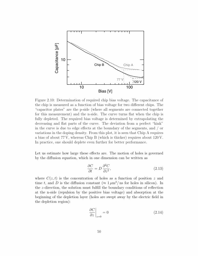
Capacitance [pF
]10
Bias [V]10010
Chip AChip B
77 V120 V
Figure 2.10: Determination of required chip bias voltage. The capacitance ofthe chip is measured as a function of bias voltage for two different chips. The“capacitor plates” are the p-side (where all segments are connected togetherfor this measurement) and the n-side. The curve turns flat when the chip isfully depleted. The required bias voltage is determined by extrapolating thedecreasing and flat parts of the curve. The deviation from a perfect “kink”in the curve is due to edge effects at the boundary of the segments, and / orvariations in the doping density. From this plot, it is seen that Chip A requiresa bias of about 77 V, whereas Chip B (which is thicker) requires about 120 V.In practice, one should deplete even further for better performance.
Let us estimate how large these effects are. The motion of holes is governedby the diffusion equation, which in one dimension can be written as
∂C
∂t= D
∂2C
∂z2, (2.13)
where C(z, t) is the concentration of holes as a function of position z andtime t, and D is the diffusion constant (≈ 1 µm2/ ns for holes in silicon). Inthe z-direction, the solution must fulfill the boundary conditions of reflectionat the n-side (repulsion by the positive bias voltage) and absorption at thebeginning of the depletion layer (holes are swept away by the electric field inthe depletion region):
∂C
∂z
∣∣∣∣z=0
= 0 (2.14)
50
and
C|z=zu= 0. (2.15)
The basic solutions of the diffusion equation with these boundary conditionscan be found by separation of variables; we assume
C(z, t) =∑
n
Zn(z) · Tn(t). (2.16)
Assuming the linear independence of the solution functions Zn(z), Eq. 2.13can be rewritten as equations
1
Tn
∂Tn
∂t=
D
Zn
∂2Zn
∂z2for all n. (2.17)
This condition must be fulfilled for all z and t, so that both sides must beequal to the same constant, which we want to denote as −Kn. If we specifythe initial condition
C(z, 0) =∑
n
Zn(z), (2.18)
we find thatC(z, t) =
∑n
e−Knt · Zn(z). (2.19)
Now we have to find Zn(z) and Kn such that
∂2Zn
∂z2= −Kn
DZn. (2.20)
The solution is given by
Zn(z) = an cos(knz) + bn sin(knz) with kn =
√Kn
D. (2.21)
From Eq. 2.14 we find that bn = 0 for all n. Eq. 2.15 then leads to
an cos(kn zu) = 0, (2.22)
which is fulfilled for all
kn =
√Kn
D=
(2n− 1) π
2zu
, n = 1, 2, 3, . . . . (2.23)
51
This defines the allowed values for Kn. In summary, we can write for theconcentration of holes
C(z, t) =∑
n
an e−Knt cos
((2n− 1) π
2zu
z
). (2.24)
The coefficients an must be picked to fulfill the initial condition of Eq. 2.18.The 1/e decay time for the terms in the above sum is given by
τn =1
Kn
=
(2zu
(2n− 1) π
)21
D. (2.25)
To estimate the time until the majority of holes is absorbed in the depletionlayer, it is sufficient to consider the n = 1 term, which decays slowest. For zu =50 µm and D = 1 µm2/ ns, the above yields τ1 ≈ 1 µs. This is much shorterthan the lifetime of electron-hole pairs in the silicon used for our chips (themean time before recombination; on the order of tens of milliseconds), so thatwe do not have to be concerned about a loss of charge due to recombination.
In Fig. 2.11, we assume a line charge distribution at t = 0 along z forz < zu, produced by high energy x-ray photons incident in a spot on thechip and creating electron-hole pairs as they penetrate into the bulk of thesilicon (we disregard the decay of intensity with penetration distance). Wehave calculated the coefficients an such that C(z, 0) is a step function, thestep ranging from z = 0 to the beginning of the depletion layer at z = 50 µm.Again, the diffusion constant is assumed to be D = 1 µm2/ ns. The plot showsthe concentration after certain time intervals. It can be seen that after about5 µs, almost all holes have been absorbed by the depletion layer. Also, it canbe seen that the higher order terms decay quickly, so that after about 300 ns,the charge distribution is approximated well by the n = 1 cosine term alone.
How about motion in the transverse direction? The x and y directions areequivalent, so that we only look at x in the following. We can again solvethe one-dimensional diffusion equation (Eq. 2.13), but this time the boundaryconditions are different; they are given by
C(x, t) = 0 for x → ±∞. (2.26)
Also, we state as initial condition that
C(x, 0) = C0 δ(x), (2.27)
where δ(x) is the Dirac delta-function. This means that at time zero, thecharge is concentrated at x = 0 and diffuses from there. It can be shown that
52

Concentr
ation o
f hole
s [a.u
.]
1.2
1.0
0.8
0.6
0.4
0.2
0.0
Profile through chip [µm]
6050403020100
5 µs
depletionlayer
t = 0
10 n
s
20 n
s
40 n
s
75 ns
150 ns300 ns600 ns
1.2 µs
2.5 µs
Figure 2.11: Diffusion of holes in undepleted silicon in the longitudinal direc-tion. We assume a step charge distribution at t = 0 in the undepleted regionof the chip, approximated by the first 1000 terms of a cosine series. Withinabout 5 µs, almost all holes have been absorbed by the depletion layer.
the solution is given by a Gaussian with a time-dependent width of
σ(t) =√
2 D t, (2.28)
or
C(x, t) =C0√
4 π D texp
(− x2
4 D t
). (2.29)
The mean distance traveled in the transverse (x, y) direction during the 1/edecay time of the z-concentration (Eq. 2.25) is then
σx = σy =√
2 D τ =√
2 D2 zu
π√
D=
√8
πzu ≈ zu, (2.30)
where we have approximated τ ≈ τ1 as above because the n = 1 term decaysslowest (i. e., we calculate more pessimistically than it is). That means we havea loss of spatial resolution on the same order as the width of the undepletedregion!
For a more accurate calculation, we can plot the charge injection profileinto the depletion layer as a function of time. As above, let us assume at time
53

Figure 2.12: Diffusion of holes in the transverse direction. At time t = 0, thedepletion layer sees a δ-function charge profile, which widens quickly. Aftera few hundred nanoseconds, almost all the charge has been absorbed by thedepletion layer.
zero, we have a line charge distribution in the z-direction extending through theundepleted region (which is assumed to be 50 µm wide), concentrated at x = 0.What is the charge profile “seen” by the depletion layer as a function of time?In the calculation above, at z = 50 µm (the start of the depletion layer), theconcentration is always zero, so that we look at z = 45 µm instead. As statedabove (Eq. 2.29), the charge profile in x is a Gaussian with a time-dependentwidth, but additionally, we have to take into account that the concentrationC0 (amount of charge) decreases exponentially as described by Eq. 2.24. Thetime-dependent charge profile in the x-direction at z = 45 µm is shown inFig. 2.12. To get the total charge injection profile in the depletion layer, wehave to integrate this curve over time, which is shown in Fig. 2.13 (scaled to amaximum of one). We can turn this curve into a probability distribution (bynormalizing it to a total area of one) and calculate the corresponding standarddeviation σ. The 2σ-width of the curve is about 28 µm; this result is roughlythe widening we expect of a focused x-ray beam in 50 µm of undepleted silicon,before the charges are captured by the electric field and driven towards the
54

Charg
e Inje
ction P
rofile
1.0
0.8
0.6
0.4
0.2
0.0
X position [µm]40200-20-40
2σ = 28 µm
Figure 2.13: Charge injection profile into the depletion layer, which is thedata of Fig. 2.12 integrated over time. If 50 µm of the chip thickness are leftundepleted, a focused x-ray beam will spread to a width of about 28 µm beforeit is “captured” by the electric field in the depletion layer.
detector segments.To measure the effect experimentally, we have scanned a 25 µm collimated
“pencil” beam across the central segment of the 9 segment chip biased with 90and then 180 V (the required bias voltage of this chip had been determined tobe about 120 V, so that at 90 V about 50 µm should be undepleted as shownin Fig. 2.9). The result is shown in Fig. 2.14. First, it can be seen that themaximum signal for the 90 V curve is lower than for the 180 V curve due toreduced quantum efficiency. As described above, this should not be due torecombination of electrons and holes in the bulk of the silicon, because there,the lifetime of charge carriers is much longer than the time for the holes tobe absorbed by the depletion region. Instead, we believe the recombination isdue to edge or surface effects, where the band structure of the semiconductormaterial changes dramatically, leading to a very different behavior than in thebulk. In other words, the assumption of perfect reflection at the n-side mightnot be fulfilled.
Second, the width of the transition region (measured from 10% to 90%of the maximum signal) when the beam moves onto and off the segment iswider for the 90 V curve than for the 180 V curve. For the 180 V curve, itis about 30 µm, on the order of the size of the beam. For the 90 V curve,it is significantly wider (about 54 µm) due to the effect of transverse motiondescribed above. In fact, we can see from the plot that due to the limitedwidth of the segment, the 90 V bias curve does not even reach its maximum
55
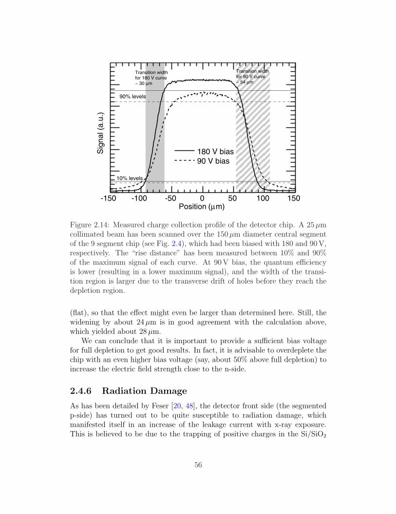
Sig
na
l (a
.u.)
Position (µm)150100500-50-100-150
90 V bias
180 V bias
90% levels
10% levels
Transition widthfor 180 V curve~ 30 µm
Transition widthfor 90 V curve~ 54 µm
Figure 2.14: Measured charge collection profile of the detector chip. A 25 µmcollimated beam has been scanned over the 150 µm diameter central segmentof the 9 segment chip (see Fig. 2.4), which had been biased with 180 and 90 V,respectively. The “rise distance” has been measured between 10% and 90%of the maximum signal of each curve. At 90 V bias, the quantum efficiencyis lower (resulting in a lower maximum signal), and the width of the transi-tion region is larger due to the transverse drift of holes before they reach thedepletion region.
(flat), so that the effect might even be larger than determined here. Still, thewidening by about 24 µm is in good agreement with the calculation above,which yielded about 28 µm.
We can conclude that it is important to provide a sufficient bias voltagefor full depletion to get good results. In fact, it is advisable to overdeplete thechip with an even higher bias voltage (say, about 50% above full depletion) toincrease the electric field strength close to the n-side.
2.4.6 Radiation Damage
As has been detailed by Feser [20, 48], the detector front side (the segmentedp-side) has turned out to be quite susceptible to radiation damage, whichmanifested itself in an increase of the leakage current with x-ray exposure.This is believed to be due to the trapping of positive charges in the Si/SiO2
56
interface just above the boron implant. Positive charges act as an n-implant,which neutralizes the p-implant and destroys the rectifying properties of thep/n-junction. The effect could be reversed by annealing (baking at about350C in a forming gas atmosphere3 for about one hour), but is undesirablefor two reasons:
• The leakage current adds to the signal and therefore has to be taken intoaccount in the calibration of the detector (see Sec. 2.6), so that a steadyincrease in leakage current would require frequent recalibration.
• Beyond a certain level, the leakage current becomes too large comparedto the actual signal current and uses up a considerable part of the dy-namic range of the integrating amplifier, leaving too little room for thex-ray signal. In fact, in the case of the soft x-ray detector, the increasein leakage current is so quick that the chip would have to be annealedevery few hours during regular operations.
Fortunately, this problem could be avoided for the NSLS detector by usingthe chip in back-side illumination mode. The back side (n-side) proved to bevery radiation-hard (any positive charges even improve the properties of then+-implant), so that even over years of operation no increase in leakage currentcould be observed.
When using the chip with harder x-rays (above a few keV), back-side il-lumination does not fully solve the problem any more. The reason is thatdue to the increased absorption length in silicon, a considerable fraction ofthe incident photons completely traverses the chip and therefore reaches theradiation-sensitive front side (see Sec. 2.4.2). We have not done a systematicmeasurement like the one described below for soft x-rays in front-side illumi-nation, but measurements of the leakage current in a test station show a clearincrease in leakage current after months or even several days of use.
Table 2.2 shows the leakage current of a new 9 segment detector chip inits initial condition, after x-ray exposure (for about 72 hours at 10 keV andat a photon flux of about 109/ s per segment for segments 2 to 5), and afterannealing at 350C for one hour. Note in particular that the leakage currentincreased strongest for segments 2 to 5 (see Fig. 2.4), the quadrant segmentswhich are covered by the beam cone during regular operation. Annealingrepairs the radiation damage and brings the leakage current back to its originallevel. In a different measurement, the leakage current of a 9 segment chip wasoriginally also on the order of 1 or 2 pA measured at 90 V bias, and after about8 months of regular use rose to 700 to 800 pA in segments 2 to 5, and 150 to300 pA in the other segments (at 180 V bias).
3a mixture of about 5% hydrogen in nitrogen
57

Seg.Leakage current (pA)
initial(new chip)
afterexposure
afterannealing
1 1.9 10.7 1.02 2.2 16 1.23 0.4 16 0.84 2.0 15 0.75 1.9 14 2.06 2.5 6.2 –a
7 1.1 7.1 0.58 1.3 13 1.29 1.6 8.2 0.7
anot measurable
Table 2.2: Leakage currents in hard x-ray radiation damage experiments. Thecurrents have been measured before and after exposure of the chip with 10 keVphotons for about 72 hours at about 109 photons per second, incident mainlyon segments 2 through 5. All leakage current measurements done at 90 V bias.
The problem is not so severe with the new electronics and the illuminationconditions present at the APS (see Table 2.1). For the 2-ID-B instrument,the maximum photon energy is 4 keV, for which the absorption length is stillshort enough to avoid exposure of the p-side to x-rays (that means, no radi-ation damage should occur, although we did not test this yet). For the otherinstruments, the signal currents are at least five orders of magnitude largerthan the initial leakage current of a new or annealed chip. In fact, the initialleakage current cannot be measured from a set of dark scans as described inSec. 2.6 due to the large feedback capacitance (for example, a current of 2 pAleads to a voltage rise of only 0.6 mV on a feedback capacitance of 33 pF after10 ms, which is below the noise level of the electronics). Therefore, even anincrease of the leakage current by two orders of magnitude can be toleratedwithout affecting the signal quality too much or using up too much of thedynamic range. Once the leakage current becomes noticeable, a dark signalmeasurement roughly every day should be enough for a good calibration. Fi-nally, the chip can be annealed every few months to bring the leakage currentback to the initial level; this is not too much of an inconvenience.
58

Radiation Damage Test of a New Front-Side Surface Treatment withSoft X-rays
As indicated by Feser [20, Sec. 3.4.2], the MPI–HLL has produced a new seriesof chips with an aluminum layer deposited directly on the silicon front side.This was expected to prevent the formation of a silicon dioxide layer andtherefore avoid radiation damage to the chip in front-side illumination at lowphoton energies.
To test this, an experiment similar to the one described by Feser [20,Sec. 3.4.2] has been performed. One of the chips (8 segment structure) hasbeen mounted and bonded for front-side illumination and for use with theNSLS version of the detector electronics. First, the leakage current was mea-sured with a picoammeter4 in a test station (see Table 2.3). The chip wasthen installed in the X1A STXM and exposed to 520 eV x-rays for about 12hours. Every 10 minutes, a set of dark measurements (x-ray shutter closed)with varying dwell times was taken, from which the leakage current can beextracted (see Sec. 2.6). The detector has been aligned such that the illumi-nation cone (projection of the zone plate) just filled the quadrant segmentsof the chip. Due to imperfect alignment of the microscope chamber, the zoneplate and therefore also the chip were not illuminated evenly. In the following,we look at the quadrant segments 4, 6 and 7, which showed the largest signals.
The extracted leakage currents are shown in Fig. 2.15. The effect of ra-diation damage is clearly seen. After about 6 hours total (about 5 hours ofexposure due to the closed-shutter periods for the dark measurements), theleakage current already saturated the electronics for the longer dwell times, soall later data is excluded from the plot.
Table 2.3 summarizes the results of the experiment. The surface dose hasbeen calculated in a manner described by Feser [20, Sec. 3.4.2]. The calculationassumes all photons are absorbed in a volume given by the area of the segmentand the absorption length of 520 eV photons in silicon. The average photonflux has been estimated from the average signal current. The actual signaldeclines over time due to the decline of the electron current in the synchrotronstorage ring.
At the end of the 12 hour exposure, the leakage current has been extractedonce more from the dark measurements, except that this time only the shorterdwell times were used since they did not saturate the electronics. The currentwas also measured again in the test station after the exposure. The chip wasthen annealed for one hour in a forming gas atmosphere at 350C. However,this degree of annealing did not completely reverse the damage as can be seen
4Keithley 487
59
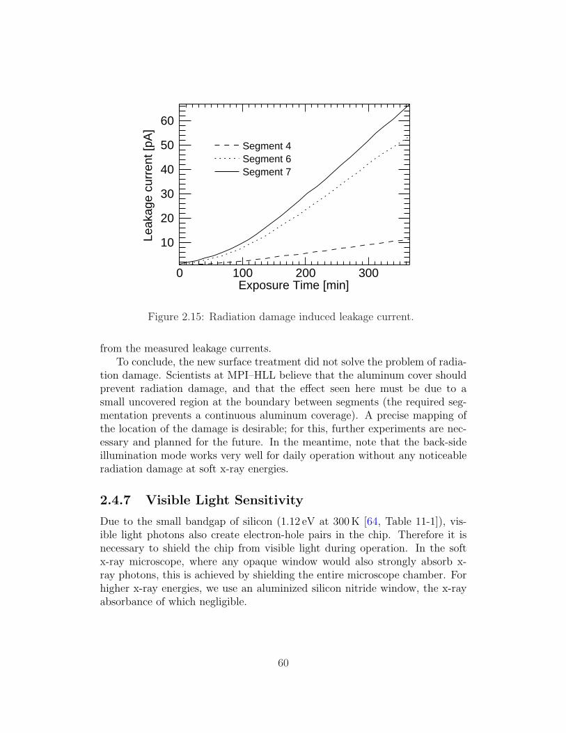
Leak
age
curr
ent [
pA]
60
50
40
30
20
10
Exposure Time [min]3002001000
Segment 7Segment 6Segment 4
Figure 2.15: Radiation damage induced leakage current.
from the measured leakage currents.To conclude, the new surface treatment did not solve the problem of radia-
tion damage. Scientists at MPI–HLL believe that the aluminum cover shouldprevent radiation damage, and that the effect seen here must be due to asmall uncovered region at the boundary between segments (the required seg-mentation prevents a continuous aluminum coverage). A precise mapping ofthe location of the damage is desirable; for this, further experiments are nec-essary and planned for the future. In the meantime, note that the back-sideillumination mode works very well for daily operation without any noticeableradiation damage at soft x-ray energies.
2.4.7 Visible Light Sensitivity
Due to the small bandgap of silicon (1.12 eV at 300 K [64, Table 11-1]), vis-ible light photons also create electron-hole pairs in the chip. Therefore it isnecessary to shield the chip from visible light during operation. In the softx-ray microscope, where any opaque window would also strongly absorb x-ray photons, this is achieved by shielding the entire microscope chamber. Forhigher x-ray energies, we use an aluminized silicon nitride window, the x-rayabsorbance of which negligible.
60

leakage current (pA)Phot.fluxa
(MHz)
Dose/Timea
(Gy/s)
Totaldoseb
(105 Gy)initialc
6 hrs ofexpos.
12 hrs ofexpos.
beforeanneal-ingd
after an-nealinge
Vbiasf 4.5 90 4.5 4.5 4.5 90 4.5 90
Seg. 4 0.1 4.7 11 22 6.4 54 –g 24 1.5 2.9 1.3Seg. 6 0.1 4.2 52 91 15 72 –g 12 6.5 12.5 5.4Seg. 7 0.2 6.4 65 109 19 86 1.2 29 8.7 16.7 7.2
aaverage during exposurebwithin 12 hours of exposurecnew chipdmeasured one day after exposureemeasured three days after annealingfbias voltage at which leakage current was measuredgnot measurable
Table 2.3: Leakage currents in soft x-ray radiation damage experiments us-ing front-side illumination. The column titled “before annealing” shows thatwithin a day after exposure, the radiation damage is already partly “healed”without annealing.
2.5 Charge Integrating Electronics
An electronic circuit was developed to integrate the charge produced in thechip during one integration cycle. The design is based on the circuit used inthe soft x-ray detector [20, 48, 59], but due to the very different illuminationconditions at the APS beamlines (see Sec. 2.3), certain modifications wererequired. A total of 10 channels is available for up to 10 detector segments.
2.5.1 Operating Principle
Fig. 2.16 shows a simplified circuit diagram of one channel. Let us have a lookat the features:
1. The detector segment is depicted on the left as a reverse-biased diode(Det) which produces a photocurrent.
2. A calibration resistor Rcal is added for testing and calibration purposes.In absense of a detector chip, a signal current can be emulated by ap-plying a voltage Ucal to the high-value calibration resistor.
3. The first amplifier stage is the inverting current amplifier A1 [68,Sec. 4.04] which
61
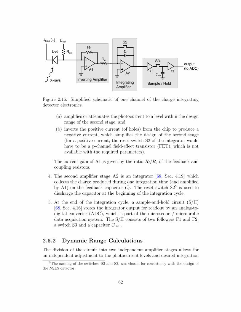
Det Rcal
Rf
Rc
Cf
A1A2
S2
Inverting AmplifierIntegratingAmplifier
Sample / Hold
S3
Ucal
output(to ADC)
Ubias (+)
X-rays
F1 F2CS/H
Figure 2.16: Simplified schematic of one channel of the charge integratingdetector electronics.
(a) amplifies or attenuates the photocurrent to a level within the designrange of the second stage, and
(b) inverts the positive current (of holes) from the chip to produce anegative current, which simplifies the design of the second stage(for a positive current, the reset switch S2 of the integrator wouldhave to be a p-channel field-effect transistor (FET), which is notavailable with the required parameters).
The current gain of A1 is given by the ratio Rf/Rc of the feedback andcoupling resistors.
4. The second amplifier stage A2 is an integrator [68, Sec. 4.19] whichcollects the charge produced during one integration time (and amplifiedby A1) on the feedback capacitor Cf . The reset switch S25 is used todischarge the capacitor at the beginning of the integration cycle.
5. At the end of the integration cycle, a sample-and-hold circuit (S/H)[68, Sec. 4.16] stores the integrator output for readout by an analog-to-digital converter (ADC), which is part of the microscope / microprobedata acquisition system. The S/H consists of two followers F1 and F2,a switch S3 and a capacitor CS/H.
2.5.2 Dynamic Range Calculations
The division of the circuit into two independent amplifier stages allows foran independent adjustment to the photocurrent levels and desired integration
5The naming of the switches, S2 and S3, was chosen for consistency with the design ofthe NSLS detector.
62
times over a wide range of conditions. The input current Iin of the system isthe photocurrent produced in the chip and given by Eq. 2.2, which we repeathere for convenience:
Iin = ε · e · Φ · E
3.62 eV, (2.31)
where ε is the photon detection efficiency of the chip, e is the charge of theelectron (1.602×10⁻¹⁹ C), Φ is the photon flux and E is the photon energy. If,instead of a detector chip, we use the calibration resistor to produce an inputcurrent, it is given by
Iin = Uin/Rcal. (2.32)
Since the inverting input of the first amplifier is at (virtual) ground level anddraws no current, its output voltage U2 is given by the photocurrent and thevalue of the feedback resistor Rf :
U2 = Rf · Iin. (2.33)
The inverting input of the second amplifier stage is again at (virtual) groundlevel, so that its input current I2 is given by the output of the first stage andthe value of the coupling resistor Rc:
I2 = U2/Rc. (2.34)
The integration time tint then determines the total amount of charge Q, andthe output voltage Uout is given by the value of the feedback capacitor Cf :
Uout =Q
Cf
=I2 · tint
Cf
. (2.35)
In summary, the total “gain” of the system can be written as
Uout =Rf
Rc · Cf
· Iin · tint. (2.36)
The value of the feedback resistor Rf is chosen such that for the maximumphotocurrent expected in a detector segment (Imax), the first amplifier reachesthe top of its output range, which was chosen to be 5 V, or
Rf = 5 V/Imax. (2.37)
The value of the feedback capacitor Cf of the integrator stage is set to 33 pF,which is an optimal value in terms of noise performance. The coupling resistorRc can be adjusted so that the integrating amplifier reaches the top of its
63

output range (again 5 V) at the maximum desired integration time tmax. Usingthe equations above, this is found to be
Rc =U2, max · tint, max
Cf · Uout, max
=tint, max
Cf
=tint, max
33 pF, (2.38)
where the maximum output voltages of the two amplifier stages cancel becausethey operate in the same range. Using the values in Table 2.1, we see that
• Rf should be in the range of 3 MΩ for high photon energy, high fluxapplications, to 300 MΩ for low photon energy, low flux applications;and
• Rc should be in the range of 10 MΩ for 0.3 ms to 100 MΩ for 3 ms inte-gration time.
2.5.3 Detector Timing and the Integration Cycle
The detector electronics system has two transistor switches per channel tocontrol the integration cycle:
1. the S2 switch which resets (discharges) the feedback capacitance of theintegrating amplifier, and
2. the S3 switch which controls the sample-and-hold circuit.
Note that because the first amplifier stage is a simple current inverting ampli-fier, it does not require any control switches.
The microscope / microprobe control system must provide a trigger pulseto the detector system to indicate the start of a new integration cycle. Thesample-and-hold circuit then switches to hold, storing the output voltage ofthe previous integration cycle for readout. A short time (1 µs) later, the S2switch closes, discharging the feedback capacitor and bringing the output ofthe integrating amplifier to zero. For a full discharge, the reset switch shouldbe closed for a few microseconds. Once the switch opens, the integrator willstart to collect all the charge delivered from the first amplifier stage and itsoutput will rise linearly with the amount of charge.
While the integration proceeds (and the S/H circuit is still on hold), thedetector electronics system sends out an acquisition pulse to the analog-to-digital converter (ADC) to read the voltage of the previous cycle from the S/Houtput. Once the readout is finished, S3 can switch to sampling (following)mode for the rest of the integration cycle. The timing pulses are provided bya commercially available pulse generator (see Sec. 2.7).
64
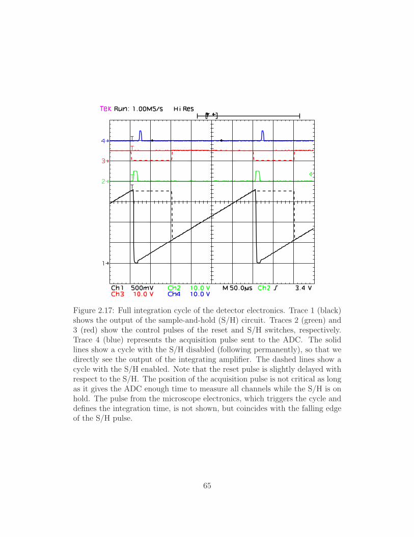
Figure 2.17: Full integration cycle of the detector electronics. Trace 1 (black)shows the output of the sample-and-hold (S/H) circuit. Traces 2 (green) and3 (red) show the control pulses of the reset and S/H switches, respectively.Trace 4 (blue) represents the acquisition pulse sent to the ADC. The solidlines show a cycle with the S/H disabled (following permanently), so that wedirectly see the output of the integrating amplifier. The dashed lines show acycle with the S/H enabled. Note that the reset pulse is slightly delayed withrespect to the S/H. The position of the acquisition pulse is not critical as longas it gives the ADC enough time to measure all channels while the S/H is onhold. The pulse from the microscope electronics, which triggers the cycle anddefines the integration time, is not shown, but coincides with the falling edgeof the S/H pulse.
65
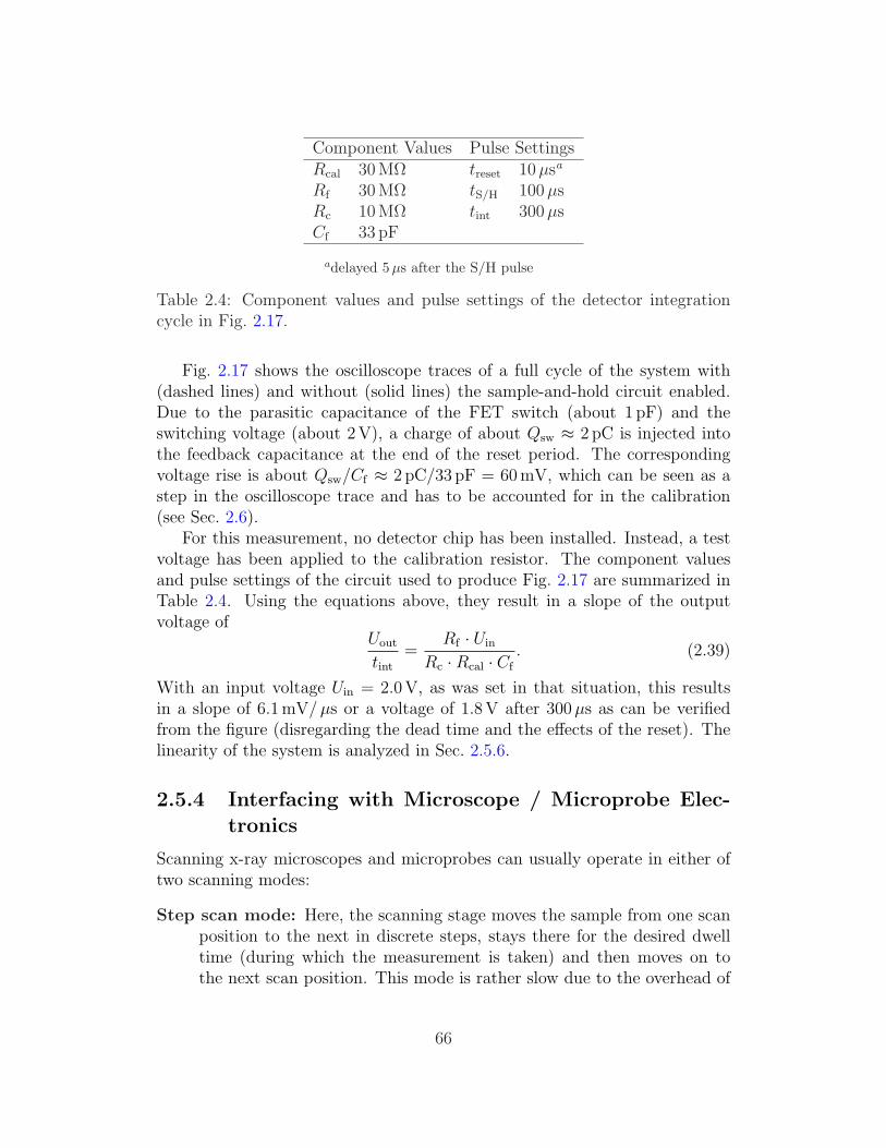
Component Values Pulse SettingsRcal 30 MΩ treset 10 µsa
Rf 30 MΩ tS/H 100 µsRc 10 MΩ tint 300 µsCf 33 pF
adelayed 5 µs after the S/H pulse
Table 2.4: Component values and pulse settings of the detector integrationcycle in Fig. 2.17.
Fig. 2.17 shows the oscilloscope traces of a full cycle of the system with(dashed lines) and without (solid lines) the sample-and-hold circuit enabled.Due to the parasitic capacitance of the FET switch (about 1 pF) and theswitching voltage (about 2 V), a charge of about Qsw ≈ 2 pC is injected intothe feedback capacitance at the end of the reset period. The correspondingvoltage rise is about Qsw/Cf ≈ 2 pC/33 pF = 60 mV, which can be seen as astep in the oscilloscope trace and has to be accounted for in the calibration(see Sec. 2.6).
For this measurement, no detector chip has been installed. Instead, a testvoltage has been applied to the calibration resistor. The component valuesand pulse settings of the circuit used to produce Fig. 2.17 are summarized inTable 2.4. Using the equations above, they result in a slope of the outputvoltage of
Uout
tint
=Rf · Uin
Rc ·Rcal · Cf
. (2.39)
With an input voltage Uin = 2.0 V, as was set in that situation, this resultsin a slope of 6.1 mV/ µs or a voltage of 1.8 V after 300 µs as can be verifiedfrom the figure (disregarding the dead time and the effects of the reset). Thelinearity of the system is analyzed in Sec. 2.5.6.
2.5.4 Interfacing with Microscope / Microprobe Elec-tronics
Scanning x-ray microscopes and microprobes can usually operate in either oftwo scanning modes:
Step scan mode: Here, the scanning stage moves the sample from one scanposition to the next in discrete steps, stays there for the desired dwelltime (during which the measurement is taken) and then moves on tothe next scan position. This mode is rather slow due to the overhead of
66

addressing, accelerating and decelerating the motor and is normally usedfor long dwell times on the order of 0.1 s and longer (e. g., for fluorescencemeasurements of trace elements, or alignment scans).
Fly scan mode: Here, the scanning stage moves continuously from the startto the end of the scan line, and a trigger at constant spatial intervalsdefines the pixels. The pixel size and the desired pixel dwell time dictatethe motor speed required. Since the motor speed can be adjusted onlywithin limits, not every combination of step size and dwell time can beachieved. Also, since the motor has to accelerate and decelerate at thestart and end of the scan line, the actual dwell time might vary andmight not match the desired dwell time for all pixels. If that is the case,a normalization of the signal to the actual dwell time for each pixel (asmeasured by a clock signal from a constant-frequency pulse generator) isstrictly required. This normalization is done almost always, even if thedwell time is nominally constant.
In either mode, the microscope / microprobe can record several data valuesfor each scan pixel, like
• 8 to 10 signals from the segments of the integrating silicon detector;
• a clock signal (the number of pulses recorded during the pixel dwell timefrom a fixed-frequency pulse generator; this is a measure of the actualdwell time for each pixel); or
• the fluorescence signal. In step scans, this can be a full spectrum at eachscan pixel (photon counts in 1024 or 2048 discrete energy bins). In flyscans, usually the total fluorescence count in a small number of energy“regions of interest” is measured.
Many more signals can be recorded in principle, like motor positions, thecurrent of the electron storage ring, the current of ion chambers to measurethe beam intensity at various places, and others. Each of those signals can beone of two types:
• a digital signal (pulse train), which is a number of pulses counted duringthe pixel integration time with a scaler (pulse counter); or
• an analog signal (voltage), which is a single reading during the pixelintegration time, done with an analog-to-digital converter (ADC).
An analog signal can also be converted to a digital signal by a voltage tofrequency converter (V2F), which produces a pulse train whose frequency de-pends on the input voltage. If such a signal is then fed into a scaler and
67

read as a digital signal, one obtains an average of the voltage during the pixelintegration time.
The triggering and interfacing of the detector electronics with the instru-ment control system is handled differently in each of the cases.
Operation in Fly-Scan Mode
The integrating electronics of the detector is designed for continuous operation;that is, an incoming trigger simultaneously signals the end of one integrationcycle and the beginning of the next one. This matches well with the fly scanmode of the microscope / microprobe and is suitable for ADC readout. Atthe beginning of the integration cycle, the signal of the previous cycle is madeavailable for readout at the output of the sample-and-hold circuit (withoutdisturbing the ongoing cycle).
This is the “natural” way to operate the detector. The microscope controlsystem has to provide a pixel-advance trigger which signals the separationbetween scan pixels. This trigger is usually extracted from the motor pulsesof the scanning stage (for stepper motors), or from the “next voltage” signalwhen a digital-to-analog converter is used to drive a piezo scanning stage.
The readout is usually handled for a whole scan line at a time by theanalog-to-digital converter of the data acquisition system, without interactionwith the rest of the control system. Usually, the ADC is “armed” by tellingit to take a certain number of readings (the number of pixels in a scan line),each reading triggered by an acquisition pulse. The trigger to the ADC isprovided by the detector electronics, with a certain delay after the incomingpixel-advance trigger. Of course the readout trigger to the ADC has to be sentout while the sample-and-hold circuit is still holding the signal of the previousscan pixel.
This adds an additional complication. In between scans, or even in betweenscan lines, the detector would not get any trigger pulse for a certain time, withthe consequence that saturation effects can occur in the first few pixels of thenext line. Therefore, an internal reset trigger is generated by the detectoritself if no external trigger arrives within a specified time. However, in thiscase no acquisition trigger should be sent to the ADC because this wouldconfuse it about the data acquisition of the next scan line. A custom firmwaremodification of the timing module takes care of this (see Sec. 2.7).
Operation in Step-Scan Mode
In step scan mode, the interfacing of the detector is less straightforward. Ide-ally, once the scanning stage has moved to a new scan pixel, one would trigger
68

Time
Vout
tint
step scan pixel step scan pixel
tdwell
motor movesto next pixel
Figure 2.18: Detector readout scheme in step scan mode. The dashed lineshows schematically the output voltage of the integrating amplifier with pe-riodic reset. The output of the sample-and-hold circuit (solid line) is “quasi-constant” due to the S/H being set to hold for most of the integration time.The pixel dwell time tdwell, indicated by the gray boxes, is much longer thanthe detector integration time tint. The short sampling period of the S/H circuitintroduces a small inaccuracy which can be neglected. In a real experiment,the signal level will of course change between scan pixels.
the detector to start integrating, trigger again at the end of the dwell timeto stop integrating and then read the signal. Although this would be possi-ble in principle, a fundamental limitation is the fact that step scan mode isusually used for long pixel dwell times (like 0.1 to 5 seconds). The dynamicrange of the detector is too limited to accommodate integration times fromsub-milliseconds for fast fly scans up such values, while at the same time beingable to accommodate signal levels (photocurrents) varying over several ordersof magnitude (also see Sec. 2.3). Therefore, we have developed a method todecouple the integration time of the detector from the pixel dwell time ofthe microscope; during a single scan pixel the detector goes through manyintegration cycles.
Fortunately, this is not complicated to achieve (see Fig. 2.18). We canuse the internal reset trigger of the detector electronics to set the detectorintegration time to a constant (a few milliseconds, matching the signal levelto the dynamic range of the detector), independent of the scanning process.The output voltage of the detector is fed into a voltage-to-frequency converterwhich puts out a pulse train. This pulse train is read by a scaler (pulse counter)whose dynamic range is only limited by the bit length of the data type usedfor counting.
Since in this case the detector output voltage is constantly measured, a“quasi-constant” signal is required. Therefore, we have to set the sample-
69
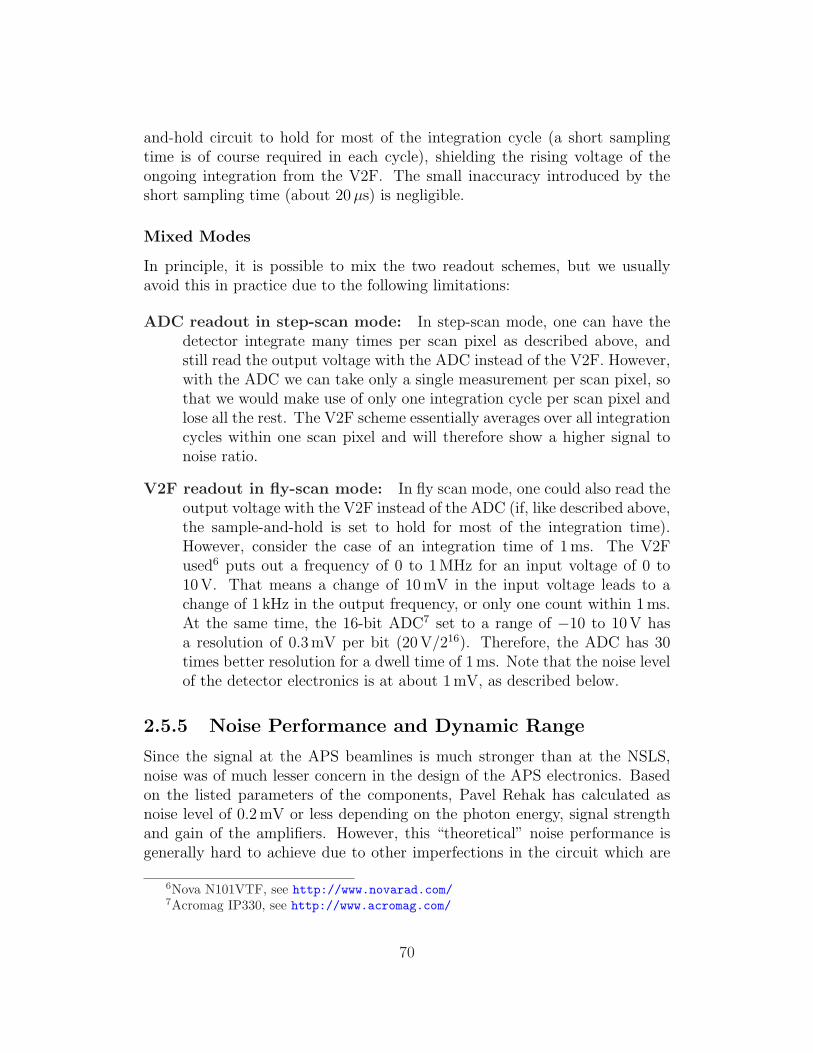
and-hold circuit to hold for most of the integration cycle (a short samplingtime is of course required in each cycle), shielding the rising voltage of theongoing integration from the V2F. The small inaccuracy introduced by theshort sampling time (about 20 µs) is negligible.
Mixed Modes
In principle, it is possible to mix the two readout schemes, but we usuallyavoid this in practice due to the following limitations:
ADC readout in step-scan mode: In step-scan mode, one can have thedetector integrate many times per scan pixel as described above, andstill read the output voltage with the ADC instead of the V2F. However,with the ADC we can take only a single measurement per scan pixel, sothat we would make use of only one integration cycle per scan pixel andlose all the rest. The V2F scheme essentially averages over all integrationcycles within one scan pixel and will therefore show a higher signal tonoise ratio.
V2F readout in fly-scan mode: In fly scan mode, one could also read theoutput voltage with the V2F instead of the ADC (if, like described above,the sample-and-hold is set to hold for most of the integration time).However, consider the case of an integration time of 1 ms. The V2Fused6 puts out a frequency of 0 to 1 MHz for an input voltage of 0 to10 V. That means a change of 10 mV in the input voltage leads to achange of 1 kHz in the output frequency, or only one count within 1 ms.At the same time, the 16-bit ADC7 set to a range of −10 to 10 V hasa resolution of 0.3 mV per bit (20 V/216). Therefore, the ADC has 30times better resolution for a dwell time of 1 ms. Note that the noise levelof the detector electronics is at about 1 mV, as described below.
2.5.5 Noise Performance and Dynamic Range
Since the signal at the APS beamlines is much stronger than at the NSLS,noise was of much lesser concern in the design of the APS electronics. Basedon the listed parameters of the components, Pavel Rehak has calculated asnoise level of 0.2 mV or less depending on the photon energy, signal strengthand gain of the amplifiers. However, this “theoretical” noise performance isgenerally hard to achieve due to other imperfections in the circuit which are
6Nova N101VTF, see http://www.novarad.com/7Acromag IP330, see http://www.acromag.com/
70
hard to quantify. From experience, a noise level on the order of 1 mV seemsreasonable for this kind of circuit.
We have tried to measure the variations in the output level of the S/Hcircuit for a constant input signal applied to the calibration resistor. Manyreadings of the S/H voltage have been taken with a multichannel analyzer(MCA)8 which can produce a histogram of sampled voltages. A Gaussian fithas been applied to the histogram, whose width (the σ-parameter) is taken asstandard deviation of the voltages. The width of the voltages measured on theS/H output was about 0.9 mV, which was the same as the variations measuredin the constant input voltage directly sampled by the MCA. Therefore, we canconclude that the noise level of the electronics is less than the accuracy ofthe measurement setup and less than 1 mV. Since the range of the amplifiersextends to 5 V, the dynamic range is better than 5000.
2.5.6 Linearity
We have also measured the linearity of the circuit with integration time aswell as with input signal. Again, no detector chip was installed; instead, a testvoltage has been applied to the calibration resistor. The output voltage and itsstandard deviation were measured with the same MCA setup as in Sec. 2.5.5above, by applying a Gaussian fit to the histogram of sampled voltages.
First, we have measured the output voltage as a function of integrationtime. The input voltage was held constant at about 3.0 V, and the integrationtime was adjusted by varying the time when the S/H switch is set to holdafter the reset. The nominal values of the components used in this setup arethe same as in Table 2.4, which gives an expected slope of about 9.1 mV/ µsaccording to Eq. 2.39. A linear least-squares fit was performed of measuredoutput voltages vs. integration time, which resulted in
Uout = (−97.33± 0.69) mV + (8.826± 0.004)mV
µs× tint. (2.40)
The reduced χ2 of the fit is 0.85; the probability of χ2 exceeding that value is0.58. The result is shown in Fig. 2.19.
Next, we have measured the output voltage as a function of input voltage,which was measured with a high-precision voltmeter.9 The integration timewas held constant at 285 µs, starting from the opening of the reset to theopening of the S/H switch. Using the nominal component parameters as aboveand rearranging Eq. 2.39 for Uout/Uin, we expect a slope of 0.86. The linear
8Oxford PCA-Multiport9Keithley 199
71
Out
put s
igna
l [V
]
2.5
2.0
1.5
1.0
0.5
0.0
Integration time [µs]300250200150100500
linear fitmeasured data
Figure 2.19: Linearity of detector electronics with integration time. The errorbars on the data are too small to display.
fit of measured output voltages vs. input voltage resulted in
Uout = (37.18± 0.57) mV + (0.8395± 0.0002)× Uin. (2.41)
The reduced χ2 is 1.8; the probability of χ2 exceeding that value is 0.06. Thisis slightly below the generally accepted value of 0.1 for the goodness-of-fit [69,Sec. 15.2] and suggests a slight nonlinearity. In fact, the residuals betweendata and fit show a sinusoidal, non-random pattern (see Fig. 2.20). However,the effect is hardly above the noise level so that it was not investigated further.
2.6 Detector Calibration
The detector can be absolutely calibrated in terms of x-ray flux, in the sameway as the NSLS detector. This has been described in detail by Feser [20,Secs. 3.4.6, 3.4.7], so that we will only summarize the important points here.It should be noted that as long as the leakage current is negligible, the rawoutput signal (voltage) is already roughly proportional to the photon signal.This is often sufficient for qualitative data analysis if the calibration softwareand parameters are not readily available.
72

Res
idua
ls [m
V]
3
2
1
0
-1
-2
-3
Out
put s
igna
l [V
]
4
3
2
1
0
Input signal [V]543210
residualslinear fitmeasured data
Figure 2.20: Linearity of detector electronics with input signal. The error barson the measured data are too small to display. The residuals (data minus fit;y axis on the right) show a sinusoidal pattern.
2.6.1 Detector Channel Crosstalk
It turns out that the 8 (or 9, or 10) signals from the detector segments are notcompletely independent. A signal in one segment can induce a small signal inone or more other channels due to capacitive coupling between the preamplifierinputs and outputs of different channels. This crosstalk is determined duringthe calibration process and then corrected for in software after data acquisitionby application of a crosstalk matrix. If S is a vector of n signals from n detectorsegments, the corrected signal Scorr is calculated as
Scorr = C S (2.42)
or
(Scorr)k =n∑
l=1
Ckl Sl, (2.43)
where C is an n× n matrix where all elements on the main diagonal Ckk = 1,and the correction coefficients outside the main diagonal are on the order of10−4 or smaller.
To determine the crosstalk coefficients, we have to induce a signal in eachsegment (channel) independently to observe the effects on the other segments.
73

6
2
Figure 2.21: Detector electronics crosstalk. Shown in both cases is the signalmeasured by segment number 6 (of the 9 segment chip), with the contrastadjusted so that faint dark features become visible (consequently washing outthe bright features). Note that the bonding pad is also visible at the bottom.Left: Uncorrected signal. Photons incident on segment number 2 have induceda small signal of opposite polarity in segment 6. The effect has been amplifiedby a factor of 5 for display purposes here. Right: After applying the crosstalkcorrection, the effect of segment 2 is removed from the signal of segment 6.
One way to do that is to record a detector map (see Figs. 2.7 and 2.8) byscanning the detector through a “pencil beam”, produced by aperturing theincoming x-ray beam with a pinhole of 10 or 20 µm diameter. Figure 2.21shows an example of the crosstalk effect and its correction. The entire crosstalkmatrix determined from the same detector map resulted in
C = 1 + 10−4 ×
0 0 0 0 0 0 0 0 00 0 0 0 0 0 0 0 00 0 0 0 0 0 0 0 00 0 0 0 0 0 0 0 00 0 0 0 0 0 0 0 00 5 0 0 0 0 0 0 00 0 5 0 0 0 0 0 00 0 0 5 0 0 0 0 00 5 0 0 0 0 0 0 0
, (2.44)
where 1 is the identity matrix. It can be seen that the effect is rather smalland restricted to a few segments, mainly determined by the proximity of theamplifiers and the conducting lines on the printed circuit board. In fact, itis rather difficult to determine the coefficients to better than a factor of two,which is why all the non-zero elements of the matrix have the same value.
74
2.6.2 Voltage to Photon Flux Conversion
Ideally, we would like to measure the average photon flux incident on eachdetector segment during the pixel dwell time. This can be achieved by theapplication of a calibration formula (after first correcting for the crosstalk asdescribed above). Despite the differences in circuit design between the NSLSand the APS detector electronics, both turn a photocurrent into an outputvoltage and can therefore use the same calibration formula. One has to takeinto account the leakage current of the chip (which adds to the photocurrent),the gain of the amplifiers, the charge injected by the opening of the reset switchand the reset (dead) time during which no integration occurs. The derivationof the calibration formula is detailed by Feser [20, Sec. 3.4.7], so that we onlywant to repeat the final result here:
Φ =F
C
Uout − U0 − C Idark tdwell
tdwell − tdead
, (2.45)
where Φ is the photon flux in s−1, Uout is the output voltage as measured bythe ADC, tdwell is the actual pixel dwell time as measured by the clock signaland all other quantities are described in the following paragraphs.
Photon-Charge Conversion Factor F
F describes how many photons are required to generate a certain amount ofcharge and is usually measured in inverse femtocoulombs. F can also includethe quantum efficiency ε of the chip (see Eq. 2.2). Since an energy of 3.62 eVis required to generate one electron-hole pair in silicon at room temperature,if we assume a quantum efficiency of one we can calculate
F =2.26× 10⁴ eV/ fC
E, (2.46)
where E is the photon energy. As an example, F = 2.26 fC−1 at E = 10 keV.
Electronics Calibration Constant C
C describes the rise of the output voltage of the integrator per charge injectedinto the circuit. Note that the name C is somewhat unfortunate, because itsunit is the inverse of a capacitance, but we keep it here for consistency with[20]. It is given by
C =Rf
Rc Cf
(2.47)
75

as derived in Sec. 2.5.2; C can be measured more precisely by measuring theslope of the output voltage for a constant calibration voltage applied to the(known) calibration resistor.
The relative accuracy of C between the different electronics channels ismore important than the absolute value. Therefore, once C has been deter-mined independently for each channel, it can be adjusted as described by Feser[20, Sec. 3.4.7]. To do that, a signal from a constant-intensity x-ray beam isinduced in each segment (by recording a detector map scan as described inSec. 2.6.1), and the C values are adjusted so that the resulting calibrated signalis the same for all segments.
Voltage Offset U0 and Dark Current Idark
Idark is the dark (leakage) current of the chip, which contributes to the signalintegrated by the electronics and therefore has to be subtracted for a propercalibration.
U0 is a voltage offset, describing the output voltage due to the leakagecurrent extrapolated to zero integration time. It takes into account the chargeinjection at the closing of the reset switch (see Sec. 2.5.3) and the fact thatcharge integration does not start at the beginning of the integration cycle butonly after the reset switch has been opened.
U0 and the product C · Idark can be determined by measuring the outputvoltage in dark conditions (no x-rays incident) for a range of dwell times andapplying a linear fit.
Dead Time tdead
The detector dead time is the time during which no charge integration takesplace and is given by the width of the reset pulse plus its delay from the closingof the S/H.
2.6.3 Calibration Procedure and Software
The full calibration procedure involves the following steps:
1. determine the crosstalk correction from a detector map file;
2. determine the dark current and voltage offset from a set of dark scans;
3. determine the dead time (from the delay and width of the reset pulse)and the photon-charge conversion factor F (in fact, we store the universalconstant of 2.26×10⁴ eV/ fC and determine F for each scan individuallyfrom its photon energy);
76
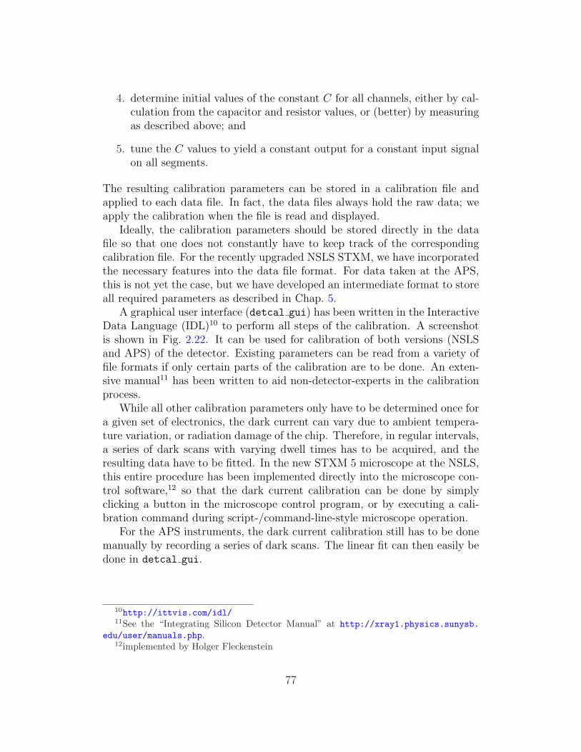
4. determine initial values of the constant C for all channels, either by cal-culation from the capacitor and resistor values, or (better) by measuringas described above; and
5. tune the C values to yield a constant output for a constant input signalon all segments.
The resulting calibration parameters can be stored in a calibration file andapplied to each data file. In fact, the data files always hold the raw data; weapply the calibration when the file is read and displayed.
Ideally, the calibration parameters should be stored directly in the datafile so that one does not constantly have to keep track of the correspondingcalibration file. For the recently upgraded NSLS STXM, we have incorporatedthe necessary features into the data file format. For data taken at the APS,this is not yet the case, but we have developed an intermediate format to storeall required parameters as described in Chap. 5.
A graphical user interface (detcal gui) has been written in the InteractiveData Language (IDL)10 to perform all steps of the calibration. A screenshotis shown in Fig. 2.22. It can be used for calibration of both versions (NSLSand APS) of the detector. Existing parameters can be read from a variety offile formats if only certain parts of the calibration are to be done. An exten-sive manual11 has been written to aid non-detector-experts in the calibrationprocess.
While all other calibration parameters only have to be determined once fora given set of electronics, the dark current can vary due to ambient tempera-ture variation, or radiation damage of the chip. Therefore, in regular intervals,a series of dark scans with varying dwell times has to be acquired, and theresulting data have to be fitted. In the new STXM 5 microscope at the NSLS,this entire procedure has been implemented directly into the microscope con-trol software,12 so that the dark current calibration can be done by simplyclicking a button in the microscope control program, or by executing a cali-bration command during script-/command-line-style microscope operation.
For the APS instruments, the dark current calibration still has to be donemanually by recording a series of dark scans. The linear fit can then easily bedone in detcal gui.
10http://ittvis.com/idl/11See the “Integrating Silicon Detector Manual” at http://xray1.physics.sunysb.
edu/user/manuals.php.12implemented by Holger Fleckenstein
77
Figure 2.22: Graphical user interface for detector calibration. In this view,the program is in the mode to perform the crosstalk correction.
78

Figure 2.23: Hardware components of the detector.
2.6.4 Verification of the Calibration
Due to the lack of an appropriate detector with absolute calibration in the x-rayenergy range of interest, the calibration could not be verified independently.However, estimates with an absolutely calibrated soft x-ray photodiode (whosethickness and therefore quantum efficiency for hard x-rays is not known well)as well as ion chambers showed consistent results within a factor of two.
Note that even for quantitative amplitude and phase measurements, anabsolute calibration is usually not required as long as the output signal isproportional to the photon flux, since the data is always normalized to theincident intensity measured in a background (specimen-free) region.
2.7 Detector Components
This section describes the hardware components of the detector. Fig. 2.23shows a photograph of the whole package.
The chip: The chip is mounted on a ceramic carrier (see Fig. 2.24), which
79

Figure 2.24: Detector chip mounted on a ceramic carrier for back-side illumi-nation. Left: Front (p-) side of the chip. Wire bonds connect the detectorsegments to the carrier pins through a cutout in the carrier. Right: Back (n-)side of the chip. This is the side where the x-rays will be incident. Only oneconnection is necessary which carries the bias voltage from the upper right pinof the carrier to the n-side of the chip. An aluminum mask shows the locationof the segments on the opposite (p-) side for orientation.
can be inserted into the socket in the front of the detector snout andwhich can therefore be exchanged easily.
The detector box: A custom-made housing holds a printed-circuit board onwhich the major part of the detector circuit is implemented, as well as astack of watch batteries to provide the chip bias voltage (see Fig. 2.25).The first amplifier stage sits on a separate, smaller board at the tip of asnout, which is small enough to fit into certain piezo stages to bring thedetector close to the specimen (at soft x-ray energies, where zone platefocal lengths and therefore working distances are short). The front ofthe snout also holds a socket into which the chip is inserted. A cap isusually put onto the snout to protect the chip and the front board, aswell as to provide electrical shielding.
The timing module: The timing module (pulse generator) is commerciallyavailable13 and provides the control pulses for the S2 and S3 switchesof the circuit as well as the acquisition pulse sent to the ADC. Thetiming module itself is triggered by the microscope electronics wheneverit advances to the next pixel (in fly scan mode), or can generate itsown trigger internally (in step scan mode, or when no external trigger
13Quantum Composers Model 9514 or equivalent
80

Figure 2.25: Detector box back side connections. Left: Back side of the detec-tor box. Several connectors feed power, the timing pulses and the calibrationvoltage to the printed circuit (PC) board, and provide the signal voltage outputfrom the electronics channels. Also, an external bias voltage can be connected.Right: Inside of the back panel. Besides the wire connections to the PC board,one can see the stack of watch batteries which provides up to 90 V bias for thesilicon chip. If the chip requires a higher bias, it has to be provided externally.
arrives). A custom firmware modification14 provides the functionality ofnot sending out an acquisition pulse in case of an automatic reset, asdescribed in Sec. 2.5.4.
The power supply: Also commercially available, a regulated DC power sup-ply15 provides stable ±6 V supply voltages for the components of thecircuit.
14Option 40315Kenwood PW36-1.5AD or equivalent
81

Chapter 3
Differential Phase Contrast
82

We have seen in Sec. 1.4 that phase gradients in the specimen refract the beamand lead to a redistribution of intensity in the detector plane of a scanningx-ray microscope or microprobe. This redistribution can be measured with aconfigured detector, like the one described in the previous chapter, to extractphase information from the specimen. In particular, the difference signal be-tween the two halves of a split detector measures the phase gradient of thespecimen (in one direction); the technique is therefore called differential phasecontrast, or DPC.
In this chapter, we want to take a more quantitative look at the signal tonoise ratio that can be obtained with DPC compared to absorption contrast athigher x-ray energies. We will also show examples of DPC images and explorethe potential of DPC to obtain quantitative phase information.
3.1 Signal to Noise Ratio in Absorption and
Differential Phase Contrast in the Refrac-
tion Model
In order to better understand the importance of differential phase contrastimaging for providing images of biological ultrastructure, we consider the fun-damental contrast that can be obtained for both absorption and phase contrastimaging. We will stay within a simple projection (for absorption contrast) andrefraction (for DPC) model; a more thorough treatment including the spatialfrequency transfer of the optical system is deferred to Chap. 4.
As described in Sec. 1.1.2, the x-ray refractive index will be written asn = 1− δ − iβ. The difference of the refractive index from unity is small: forprotein at 10 keV, δ = 3.0 × 10⁻⁶ and β = 5.4 × 10⁻⁹ using the tabulation ofHenke et al. [9]. While both of these are small quantities, the fact that thereal part δ is much larger than the imaginary part β means that the phaseadvance exp(iδkt) of a feature can be much larger than its intensity attenuationexp(−2βkt). Here, k = 2π/λ is the wave number, and t is the thickness of thefeature.
3.1.1 Signal to Noise Ratio in Absorption Contrast
Let us assume we have a normalized signal If when a feature is present anda background intensity Ib when the feature is absent. Then, the photon-statistics-limited signal to noise ratio (SNR) obtained with N illuminatingphotons per pixel is given by [70, 71] the difference in the signal divided bythe root-mean-squared sum of the uncorrelated errors in each measurement,
83

or
SNR =Signal
Noise
=|NIf −NIb|√(√NIf
)2+
(√NIb
)2
=√
N|If − Ib|√
If + Ib
=√
NΘ, (3.1)
where we have used the Gaussian approximation to Poisson statistics (whichis quite good for NI greater than about 10; see Sec. 1.3.1) and the assumptionthat there are no other noise sources with significant fluctuations. The contrastparameter
Θ =|If − Ib|√
If + Ib
(3.2)
is different from the usual definition of contrast due to the square root in thedenominator. With this definition, the number of photons required to see afeature with a desired signal to noise ratio SNR is given by
N =
(SNR
Θ
)2
, (3.3)
and a common choice for the minimum detectable signal to noise ratio is theRose criterion of SNR = 5 [23].
For weak absorption contrast, where I = I0 exp (−2kβt) ≈ I0 (1− 2kβt)in a thickness t of material, we can calculate the contrast parameter based onmeasuring the absorption either in a feature-containing region or in a back-ground region. In this case the contrast parameter becomes
Θabs ≈√
I02 |βf − βb| kt√
2− 2 (βf + βb) kt
≈√
2I0|βf − βb| kt
1− 12(βf + βb) kt
≈√
2 (2π) |βf − βb| t
λ, (3.4)
where in the final form we have assumed I0 = 1 which is consistent with thesignal error being
√NI.
84

b f
θr
t
∆r
Figure 3.1: Refraction from a transition from feature (f) to background (b)materials over a width ∆r.
3.1.2 Signal to Noise Ratio in Differential Phase Con-trast
Let us now consider differential phase contrast imaging of the transition be-tween two regions with different refractive indices as shown in Fig. 3.1. Weassume that the transition occurs over the width of the probe ∆r, and we willstart by considering the refraction angle of an x-ray beam when it encountersthis transition. The refraction angle due to a small phase gradient dφ/ dx ¿ k(which we assume to be constant over the probe width) is
θr =1
k
dφ
dx. (3.5)
The phase advance imposed on a wave by a material of thickness t is δkt (seeSec. 1.1.3). Therefore, the refraction angle associated with a change in phase∆φ between two material types over the width ∆r is given by
θr =1
k
∆φ
∆r
=1
k
|δf − δb| k t
∆r
= |δf − δb| t
∆r(3.6)
as illustrated in Fig. 3.1. This refraction angle is small compared to the semiangle θZP = λ/(2 drN) (see Eq. 1.23) into which light emerges from the focus ofa zone plate with finest outermost zone width drN, as shown in Fig. 3.2. If thedetector is split into two separate segments along the line of the optical axis,and when we have a feature (the transition between two materials) present, thesignal in the two detector half-planes becomes N (I0/2) (1± θr/θZP) so that
85

optic
verticallysplit detector
object withphase gradient
θZP θr
Figure 3.2: Refraction of the beam cone emerging from the focus of an opticin a scanning microscope due to a phase gradient in the specimen.
the signal difference between the two planes with θr/θZP fractional changesbecomes NI0 θr/θZP. What is the signal variance in each case? When thefeature is present but weak, the square root of the variance in total signalmeasured in either detector segment is given by
√NI0/2 so the net error is√
NI0. When the feature is absent, the net error is again√
NI0. Since theseerrors are due to uncorrelated photon statistics, the net signal to noise ratiofor differential phase contrast imaging becomes
SNRDPC =NI0 θr/θZP√
2NI0
, (3.7)
so that we can write the contrast parameter as
ΘDPC =SNR√
N=
1√2
θr
θZP
, (3.8)
where again we have assumed I0 = 1. We can now insert our results for θr
and θZP and find that the contrast parameter for differential phase contrastimaging becomes
ΘDPC =1√2
θr
θZP
=1√2
(|δf − δb| t
∆r
)(2 drN
λ
)
≈√
2 |δf − δb| t
λ, (3.9)
where we have set ∆r ≈ drN from Eq. 1.24.
86
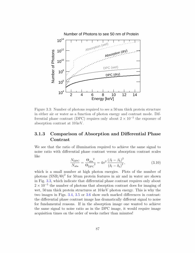
Num
ber
of P
hoto
ns
1014
1012
1010
108
106
104
Energy [keV]1412108642
DPC (dry)
DPC (wet)
Absorption (dry)Absorption (wet)
Number of Photons to see 50 nm of Protein
Figure 3.3: Number of photons required to see a 50 nm thick protein structurein either air or water as a function of photon energy and contrast mode. Dif-ferential phase contrast (DPC) requires only about 2 × 10⁻⁵ the exposure ofabsorption contrast at 10 keV.
3.1.3 Comparison of Absorption and Differential PhaseContrast
We see that the ratio of illumination required to achieve the same signal tonoise ratio with differential phase contrast versus absorption contrast scaleslike
NDPC
Nabs
=Θ 2
abs
Θ 2DPC
= 4π2 (βf − βb)2
(δf − δb)2 , (3.10)
which is a small number at high photon energies. Plots of the number ofphotons (SNR/Θ)2 for 50 nm protein features in air and in water are shownin Fig. 3.3, which indicate that differential phase contrast requires only about2× 10−5 the number of photons that absorption contrast does for imaging ofwet, 50 nm thick protein structures at 10 keV photon energy. This is why thetwo images in Figs. 3.4, 3.5 or 3.6 show such marked differences in contrast:the differential phase contrast image has dramatically different signal to noisefor fundamental reasons. If in the absorption image one wanted to achievethe same signal to noise ratio as in the DPC image, it would require imageacquisition times on the order of weeks rather than minutes!
87
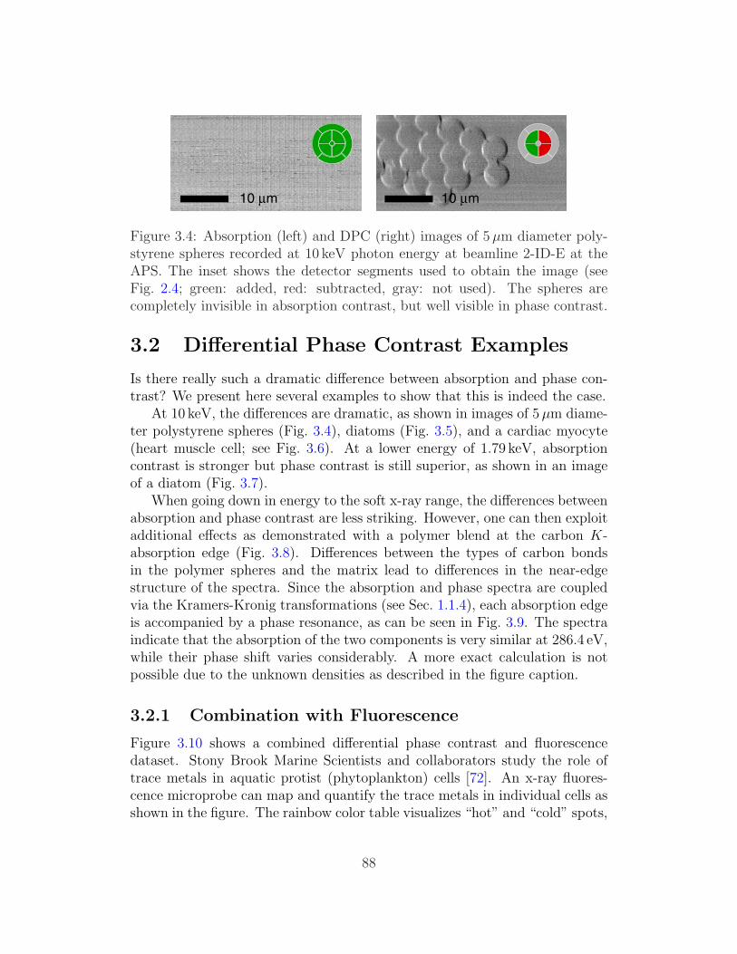
10 µm 10 µm
Figure 3.4: Absorption (left) and DPC (right) images of 5 µm diameter poly-styrene spheres recorded at 10 keV photon energy at beamline 2-ID-E at theAPS. The inset shows the detector segments used to obtain the image (seeFig. 2.4; green: added, red: subtracted, gray: not used). The spheres arecompletely invisible in absorption contrast, but well visible in phase contrast.
3.2 Differential Phase Contrast Examples
Is there really such a dramatic difference between absorption and phase con-trast? We present here several examples to show that this is indeed the case.
At 10 keV, the differences are dramatic, as shown in images of 5 µm diame-ter polystyrene spheres (Fig. 3.4), diatoms (Fig. 3.5), and a cardiac myocyte(heart muscle cell; see Fig. 3.6). At a lower energy of 1.79 keV, absorptioncontrast is stronger but phase contrast is still superior, as shown in an imageof a diatom (Fig. 3.7).
When going down in energy to the soft x-ray range, the differences betweenabsorption and phase contrast are less striking. However, one can then exploitadditional effects as demonstrated with a polymer blend at the carbon K-absorption edge (Fig. 3.8). Differences between the types of carbon bondsin the polymer spheres and the matrix lead to differences in the near-edgestructure of the spectra. Since the absorption and phase spectra are coupledvia the Kramers-Kronig transformations (see Sec. 1.1.4), each absorption edgeis accompanied by a phase resonance, as can be seen in Fig. 3.9. The spectraindicate that the absorption of the two components is very similar at 286.4 eV,while their phase shift varies considerably. A more exact calculation is notpossible due to the unknown densities as described in the figure caption.
3.2.1 Combination with Fluorescence
Figure 3.10 shows a combined differential phase contrast and fluorescencedataset. Stony Brook Marine Scientists and collaborators study the role oftrace metals in aquatic protist (phytoplankton) cells [72]. An x-ray fluores-cence microprobe can map and quantify the trace metals in individual cells asshown in the figure. The rainbow color table visualizes “hot” and “cold” spots,
88

5.0 µm 5.0 µm
Figure 3.5: Absorption and DPC images of diatoms (phytoplankton cells) at10 keV photon energy, recorded at beamline 2-ID-E at the APS. As above, thespecimens are completely invisible in absorption, but clearly visible in phasecontrast. Sample courtesy of Ben Twining and Stephen Baines, Stony BrookMarine Sciences.
while the data values provide absolute amounts of each element in µg/cm2.When using the configured detector, low resolution differential phase con-
trast is available in parallel as shown in the image labeled “dpchor.” A separatefast fly scan, highlighted by the green box, provides a high resolution, highcontrast transmission image of the same cell and visualizes specimen ultra-structure in much more detail. The acquisition of the 601 by 501 pixel DPCfly scan (50 nm steps) with 2 ms dwell time took about 25 minutes, while the56 by 51 pixel fluorescence step scan (400 nm steps) with 1 s dwell time tookabout 70 minutes.
In the future, we expect to be able to provide the absolute phase shiftof the specimen using the method described in Chap. 4. This can in turnprovide specimen thickness and mass to convert trace element amounts toconcentrations.
Absorption contrast shows a weak outline of the cell in the fluorescencescan due to the long dwell time (see the image labeled “absic” for the absorp-tion signal based on ion chamber detectors). When using short dwell times(this includes finder scans to locate individual cells), the cells are completelyinvisible in absorption contrast, similar to Fig. 3.5.
89

20 µm 20 µm
Figure 3.6: Absorption (left) and DPC (right) images of a cardiac myocyterecorded at 10 keV photon energy at beamline 2-ID-E at the APS. Whilethe specimen is relatively thick and therefore visible in absorption contrast(here recorded with an ion chamber rather than the segmented detector), thephase contrast image shows considerably more detail, in particular the cross-striations typical of heart muscle. Sample provided by B. Palmer, U. Vermont.Image recorded by Stefan Vogt, Advanced Photon Source, with the modifiedsoft x-ray detector (Sec. 2.2).
5.0 µm 5.0 µm
Figure 3.7: Absorption (left) and DPC (right) images of a diatom (phyto-plankton cell) recorded at 1790 eV photon energy at beamline 2-ID-B at theAPS. This image was also obtained with the modified soft x-ray detector.While the specimen is visible in absorption, the DPC image shows consider-ably more detail. The diagonal line visible in both images is the edge of asilicon nitride window. The horizontal line is due to a sudden change in x-rayintensity; thus it is almost invisible in the differential measurement. Imagetaken with Michael Feser, then of Stony Brook, and David Paterson, then ofAPS.
90

1.0 µm 1.0 µm
Figure 3.8: Absorption (left) and DPC (right) images of a polymer blend(spheres embedded in a matrix) at 286.4 eV photon energy. At this particularenergy (in the vicinity of the carbon K-absorption edge), the imaginary partβ of the refractive index is the same for the two kinds of polymers, so thatthe absorption image does not show any contrast. The real part δ, however, isdifferent so that we get good phase contrast despite the noisy signal. Samplecourtesy of Gary Mitchell, Dow Chemical.
91

f 1,
f 2
1.0
0.8
0.6
0.4
0.2
0.0
-0.2
Photon energy [eV]310300290280270
Kramers-Kronig Transform of Polymer Blend
matrix f2
matrix f1
spheres f2
spheres f1
286.4
eV
Figure 3.9: Absorption and phase spectra of the polymer blend shown inFig. 3.8. Shown are the real and imaginary parts of the complex oscillatorstrength (which are related to the complex refractive index by Eqs. 1.5 and 1.6)normalized by the number of electrons. The imaginary part f2 was obtainedfrom a near-edge absorption spectrum. Then, the real part f1 was calculated byusing the Kramers-Kronig transformations and a combination of the measurednear-edge data and tabulated absorption data as described by Jacobsen et al.[33]. We assume that the number densities of electrons of the two componentsare similar (the actual mass densities are not known), so that the normalizedoscillator strengths are roughly proportional to δ and β (which determineabsorption and phase shift). It can be seen that at around 286.4 eV, where theimages in Fig. 3.8 were taken, the normalized f2 values are very similar, whilethere is a considerable difference in the f1 values. Therefore, the spheres areclearly visible in phase contrast, whereas they are not in absorption contrast.
92

absic 0.787-0.773
S
Mn 0.00 - 0.025 µg/cm2
dpccfg 0.955-0.911
Cl 0.00 - 1.06 µg/cm2
Fe 0.00 - 0.606 µg/cm2
K 0.00 - 0.368 µg/cm2
Cu 0.00 - 0.023 µg/cm2
Si 0.0 - 182 µg/cm2
Ca 0.01 - 8.59 µg/cm2
Zn 0.00 - 0.343 µg/cm2
P 0.0 - 16.7 µg/cm2
Ti 0.00 - 0.018 µg/cm2
sa 402 - 5767 cts/s
10 µm MAPS V1.5.1.0
0.01 - 7.86 µg/cm2
Fly Scan DPC
Figure 3.10: Differential phase contrast and fluorescence images of a phy-toplankton cell Cyclotella (see text). Sample provided by Stephen Baines,Stony Brook Marine Sciences. Fluorescence data processing by Stefan Vogt,Advanced Photon Source.
93
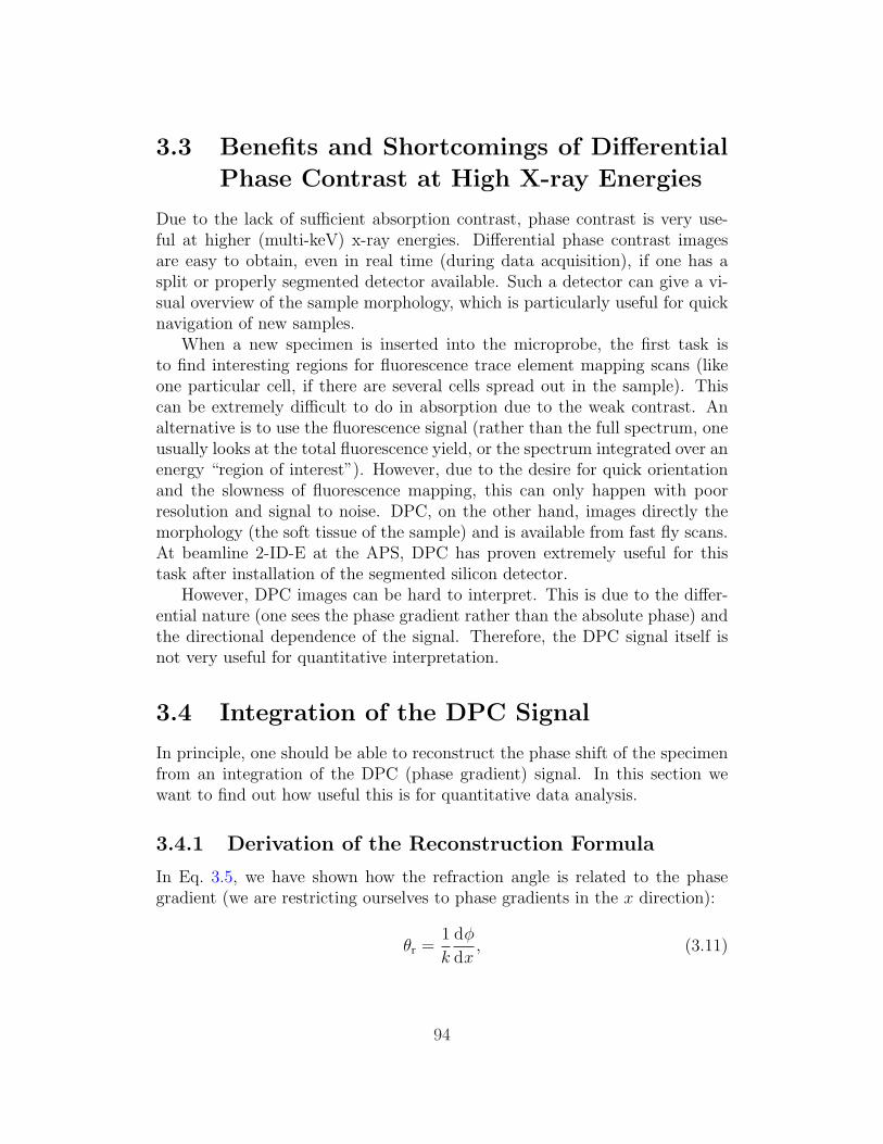
3.3 Benefits and Shortcomings of Differential
Phase Contrast at High X-ray Energies
Due to the lack of sufficient absorption contrast, phase contrast is very use-ful at higher (multi-keV) x-ray energies. Differential phase contrast imagesare easy to obtain, even in real time (during data acquisition), if one has asplit or properly segmented detector available. Such a detector can give a vi-sual overview of the sample morphology, which is particularly useful for quicknavigation of new samples.
When a new specimen is inserted into the microprobe, the first task isto find interesting regions for fluorescence trace element mapping scans (likeone particular cell, if there are several cells spread out in the sample). Thiscan be extremely difficult to do in absorption due to the weak contrast. Analternative is to use the fluorescence signal (rather than the full spectrum, oneusually looks at the total fluorescence yield, or the spectrum integrated over anenergy “region of interest”). However, due to the desire for quick orientationand the slowness of fluorescence mapping, this can only happen with poorresolution and signal to noise. DPC, on the other hand, images directly themorphology (the soft tissue of the sample) and is available from fast fly scans.At beamline 2-ID-E at the APS, DPC has proven extremely useful for thistask after installation of the segmented silicon detector.
However, DPC images can be hard to interpret. This is due to the differ-ential nature (one sees the phase gradient rather than the absolute phase) andthe directional dependence of the signal. Therefore, the DPC signal itself isnot very useful for quantitative interpretation.
3.4 Integration of the DPC Signal
In principle, one should be able to reconstruct the phase shift of the specimenfrom an integration of the DPC (phase gradient) signal. In this section wewant to find out how useful this is for quantitative data analysis.
3.4.1 Derivation of the Reconstruction Formula
In Eq. 3.5, we have shown how the refraction angle is related to the phasegradient (we are restricting ourselves to phase gradients in the x direction):
θr =1
k
dφ
dx, (3.11)
94
θZPθr
d
object with
phase gradient
zone plate
a
detector
planex
z
Figure 3.11: Shift of the beam cone on the detector. We assume a zone plateoptic with a central stop, as is commonly used in scanning x-ray microscopy.On the right, the detector segments are tinted in dark gray, whereas the foot-print of the beam is shown unshifted and shifted as a light gray overlay. Thehatched area corresponds to the intensity which is shifted across the boundarybetween the two half planes of the detector when a sample with a phase gra-dient is present. The detector consists of four annular quadrant segments anda central segment, corresponding to the center part of the 9-segment chip (seeSec. 2.4). The center segment is located in the shadow region of the centralstop and thus does not affect the signal.
where φ = δkt is the total phase advance of the specimen relative to vacuumpropagation (the quantity we wish to calculate), and k = 2π/λ is the wavenumber. Let us now consider the case of an optic with a central stop, as iscommonly used in scanning x-ray microscopy, and a segmented detector withfour annular quadrants as illustrated in Fig. 3.11. A sample with a phasegradient will refract the beam, leading to a shift of the beam footprint on thedetector chip. Let us further assume that the beam shift is small and that thebeam will always stay on the annular quadrant structure.
We only consider phase gradients in one direction, so that we can combinethe four quadrant segments into two half plane signals, indexed by 1 and 2.If a total of N photons is incident per scan pixel, equally distributed overthe pupil of the optic, then the intensity on each of the half planes will beI1 = I2 = N/2 for an unrefracted beam (zero phase gradient).
If the beam is refracted by an angle θr, it will be shifted on the detectorchip by an amount a = θr · d, where d is the distance from the focus to thedetector. If fstop is the diameter of the central stop relative to the total pupildiameter, the outer and inner radius of the beam annulus on the detector chipare given by θZP · d and fstop · θZP · d, respectively. The half opening angle of
95

the zone plate is the numerical aperture
NA = θZP =λ
2 drN
, (3.12)
where drN is the outermost zone width (see Eq. 1.23). Then the number ofphotons which is shifted from the lower to the upper half is given by the ratioof the hatched area to the total area of the beam (see Fig. 3.11):
Ishifted = N × 2 a (1− fstop) d θZP
π (d θZP)2 (1− f 2stop)
= N × 2 θr
π θZP (1 + fstop). (3.13)
The intensity in each of the half planes becomes
I1, 2 = N ×(
1
2± 2 θr
π θZP (1 + fstop)
), (3.14)
so that the signal difference, which is the final DPC signal, becomes
IDPC = I1 − I2 =4 N θr
π θZP (1 + fstop). (3.15)
We can normalize by the absorption image (which is N , the total number ofphotons measured by the detector for each scan pixel)
IDPC, norm =IDPC
N, (3.16)
solve for the refraction angle and use Eqs. 3.11 and 3.12 to calculate the phasegradient:
dφ
dx=
π2
4
(1 + fstop)
drN
× IDPC, norm. (3.17)
The total phase shift is then available by integration across the image:
δkt = φ =
∫dφ
dxdx. (3.18)
Let us also point out again that for a first-moment detector (whose responseis proportional to the distance from the optical axis in either x or y, so that itmeasures the true “center of mass” of intensity), the signal is proportional tothe phase gradient even for strong gradients [45, 46]. For the split (segmented)
96
detector as described here, this is only true for weak gradients, where the shiftof the beam is small compared to the beam diameter (see Fig. 3.11). How-ever, the segmented detector offers practical advantages over a first-momentimplementation as described in Secs. 1.4.2 and 2.1.
3.4.2 Simulations with Noise-free Data
To explore the possibilities of phase recovery from the integration of DPCimages, we begin by carrying out simulations with ideal, noise-free data. Weare using the following parameters:
• The specimen is a perfect sphere of 1.6 µm diameter with a maximumphase shift (at its center) of δkt = 0.1 and zero absorption.
• The image is simulated on a 96×96 pixel grid with a pixel size of 50 nm.
• The x-ray energy is assumed to be 10 keV.
• The zone plate has an outermost zone width of drN = 100 nm and acentral stop with a diameter of 0.3 times the zone plate diameter.
• The detector chip, and the alignment of the beam with respect to thedetector chip, are as in Fig. 3.11.
• A total of 105 photons are incident per scan pixel, equally distributedover the zone plate pupil.
We have simulated the imaging process as described in Chap. 4 (Eq. 4.6), tak-ing into account the effects (limited frequency transfer) of the optical system.Figure 3.12 shows the total phase shift of the simulated specimen, the sim-ulated noise-free normalized DPC image (showing the phase gradient in thex-direction) and the total phase shift reconstructed from the DPC signal byintegration. Considering that the reconstruction process by integration, basedon a simple refraction model, does not take into account any diffraction effectsof the optical system, the result is surprisingly good.
3.4.3 Simulations with Noisy Data
Even in a perfect setup, real images will always be subject to photon noise (seeSec. 1.3.1). Since the signal to noise ratio is proportional to the square rootof the total photon count in a given segment (if photon noise is the dominantnoise source; i. e., other noise can be neglected), the noise can be reducedby illuminating the sample with more photons, such as by using a stronger
97

1.0 µm
min = 0.000
max = 0.100
min = −0.015
max = 0.015
1.0 µm 1.0 µm
min = −0.005
max = 0.093
Figure 3.12: Phase reconstruction by integration of a simulated noise-free DPCsignal. All quantities are shown on a linear gray scale between the minimum(black) and maximum (white) specified. Left: Total phase shift δkt of thesimulated sphere specimen. Center: Ideal (noise-free) normalized DPC signal(see Eq. 3.16). Right: Total phase shift δkt obtained by integration of theDPC signal according to Eq. 3.18.
source or illuminating for a longer time. A compromise is required betweena sufficient signal to noise ratio on the one hand and short data acquisitiontimes and reduced radiation damage on the other.
In practice, other noise sources (beam motion, vibration of optical elements,detector noise etc.) are present as well, so that it is usually difficult to achievephoton-limited statistics.
Therefore, it is instructive to carry out the same simulations as in the pre-vious section, but in the presence of noise. We have applied random Poisson-distributed noise to the images obtained in the previous section and repeatedthe integration of the DPC signal. Figure 3.13 shows the resulting normal-ized DPC signal and the total phase shift δkt obtained by integration. It isapparent that the noise introduces unwanted streaks in the final result, sinceevery deviation of a single pixel from the mean carries through a whole lineunless it is offset by an opposite pixel. Note in the upper right picture how allscan lines start on common level on the left side, but how they diverge to theright, along the direction of integration. This effect can be somewhat reducedby averaging the integration in opposite directions, as well as including thevertical DPC signal (see the bottom row in Fig. 3.13), but cannot be fullyeliminated. Several pre- and post-integration filters have been tried, withoutmuch effect other than reducing the actual data content.
98

min = −0.019
max = 0.020
1.0 µm 1.0 µm
min = −0.139
max = 0.172
sphere center mean = 0.098
background mean = −0.003
1.0 µm
min = −0.090
max = 0.149
sphere center mean = 0.107
background mean = 0.000
1.0 µm
min = −0.062
max = 0.141
sphere center mean = 0.103
background mean = −0.002
Figure 3.13: Phase reconstruction by integration of a simulated noisy DPCsignal. All quantities are shown on a linear gray scale between the minimum(black) and maximum (white) specified. For the integrated DPC signals, themean of the center region of the sphere, as well as the mean of part of thebackground region (as marked by the red circles), is given as well. Upper left:Normalized DPC signal. Upper right: Total phase shift obtained by integrat-ing the DPC signal from left to right. Lower left: Average of the integrationin both horizontal directions. Lower right: Average of the integration in bothhorizontal and both vertical directions.
3.4.4 Integration of Real Data
Further complications arise with real, as opposed to simulated, data, in theform of uneven illumination of the detector segments. Consider the imagetaken of two 5 µm diameter polystyrene spheres shown in Fig. 3.14. Theimage was recorded at the 2-ID-E beamline at the APS, at an x-ray energyof 10 keV and using a 110 µm diameter zone plate with a 40 µm central stopand an outermost zone width of 164 nm (see Sec. 4.6.1). Using the tabulateddata of Henke et al. [9], we expect a total phase shift of δkt = 0.60 for 5 µmof polystyrene.
In Fig. 3.15 we show a map of the beam (the intensity transmitted bythe zone plate, projected across the focus to the detector plane) used for theacquisition of the polystyrene sphere images. It was obtained by scanning the
99

2.5 µm
min = 0.024
max = 0.126
2.5 µm
min = 0.091
max = 26.6
2.5 µm
min = −1.90
max = 1.40
sphere center mean = 0.920
background mean = −0.025
Figure 3.14: Phase reconstruction by integration of a real DPC image. Allquantities are shown on a linear gray scale between the minimum (black) andthe maximum (white) specified. Left: Horizontal DPC signal. Note howthe minimum and maximum data values are not symmetrical around zero (asopposed to the DPC image in Fig. 3.13) due to the uneven background levelof the segments. Center: DPC signal integrated horizontally as in Sec. 3.4.3.The offset in the DPC background region leads to a strong “ramp background”in the integrated image against which the actual spheres are too weak tostand out. Right: Integrated DPC image after background-equalizing the rawimages.
detector, apertured with a 15 µm pinhole, with no sample present. As canbe seen, the beam has a “blind spot” covering almost 10% of its area. Thisis most likely due to a piece of dust on the monochromator crystal. Whenthe detector is aligned for data taking, the blind spot leads to one quadrantsegment being illuminated much more weakly than the others, and therefore toan uneven background level between segments and an offset in the DPC image(ideally, the background in the DPC image should have an intensity differenceof zero, with the feature values being spread symmetrically around zero forsymmetrical specimens). Additionally, any slight misalignment of the detector(which cannot be avoided in practice, since the precision of the detector stageis only around one micron) contributes to these uneven background levels.
The center image in Fig. 3.14 shows the DPC image integrated by the samemethod as in the previous section. The background offset as described in theprevious paragraph leads to a strong “ramp background” when integrated.The signal variation due to the actual specimen (the two spheres) is too weakto even be noticeable in the image.
This problem can be addressed by normalizing, that is, by scaling thequadrant signals to a common background level before integrating. The resultis shown on the right in Fig. 3.14. Even though the spheres are now visible,and the resulting phase shift in the sphere center is within 50% of the expected
100

100 µm
Figure 3.15: Map of the beam in the detector plane. This image was obtainedby scanning the detector (without any specimen being present), which at thesame time was apertured with a 15 µm diameter pinhole. Only the signal ofsegment 3 is shown, over which the pinhole was located. One can clearly seethe “blind spot” in the zone plate, which leads to an uneven illumination ofthe quadrant detector segments. The slightly elliptical appearance of the pupilis due to a wrong setting of the step size of the motorized detector stage; theactual zone plate is circular.
value, the result is not really satisfying.
3.4.5 Conclusions
We have seen that differential phase contrast is very useful for quick overviewimages in a scanning microscope or microprobe, to locate interesting sampleregions and to get a qualitative map of sample morphology. However, itsusefulness is limited if quantitative information is desired. A straight one-dimensional integration of the DPC signal, even when combining two orthog-onal directions, does not cope with noise very well and has difficulties if thebackground level is uneven between segments.
More elaborate methods for the integration of orthogonal gradient dataexist or are being developed [73–75], and they might prove quite useful forsolving the problem presented here. Note, however, that none of these takeinto account the diffraction effects (limited frequency transfer) of the opticalsystem. Therefore, in the following chapter we want to analyze the imagingprocess in a scanning microscope in more detail, and we will present whatwe believe to be a superior approach for phase reconstruction from segmenteddetector data in the presence of noise.
101

Chapter 4
Quantitative Amplitude andPhase Reconstruction fromSegmented Detector Data
102

In this chapter, we describe the use of a Fourier filtering method [76–79] de-veloped for scanning transmission electron microscopy (STEM) to obtain si-multaneously quantitative absorption and phase contrast images from a singlemeasurement of the specimen with a segmented detector. We have recentlypublished the essence of the method and its application in soft x-ray STXM[80].
Table 4.1 lists the symbols and quantities used in this chapter for refer-ence. Also, we will make extensive use of Fourier transform (FT) relations; seeAppendix B for a summary of the important properties and definitions usedhere. In this chapter, we will only show the important steps of the image for-mation and specimen reconstruction procedure; a detailed derivation is givenin Appendix D.
4.1 Image Formation in a Scanning Transmis-
sion X-ray Microscope
The theory of image formation in STXM with a segmented detector has beendescribed before [29, 53], based on the extensive expertise from the field ofSTEM (see, e.g., [35, 81–83]). A good description of the incoherent imagingprocess (including the TXM) has also been given by Vogt et al. [32]. Herewe want to review the important steps in a suitable form for later use. Wewill do so in the convention that waves forward propagate as exp[−i(kz −ωt)]. Consequently, inverse Fourier transforms are used to propagate waves,as opposed to forward transforms in the convention used by Goodman [14].
4.1.1 Wave Propagation to the Detector Plane
In STXM, the specimen is raster-scanned through a focused x-ray beam, andthe transmitted intensity is measured by a detector for each scan position asillustrated in Fig. 4.1. The focusing optic, in our case a Fresnel zone plate orZP (see Sec. 1.2.3), is coherently illuminated, and the complex scalar wavefieldwithin the aperture of the optic is represented by the pupil function P (f
ZP).
It is convenient for Fourier transform notation to use spatial frequency coor-dinates f in the zone plate and detector planes, which relate to real spacecoordinates r as
f =r
λz, (4.1)
where λ is the x-ray wavelength and z the propagation distance under consider-ation. Spatial frequency coordinates in the pupil and detector plane essentiallyrelate real space coordinates to diffraction angle; in other words, the optical
103
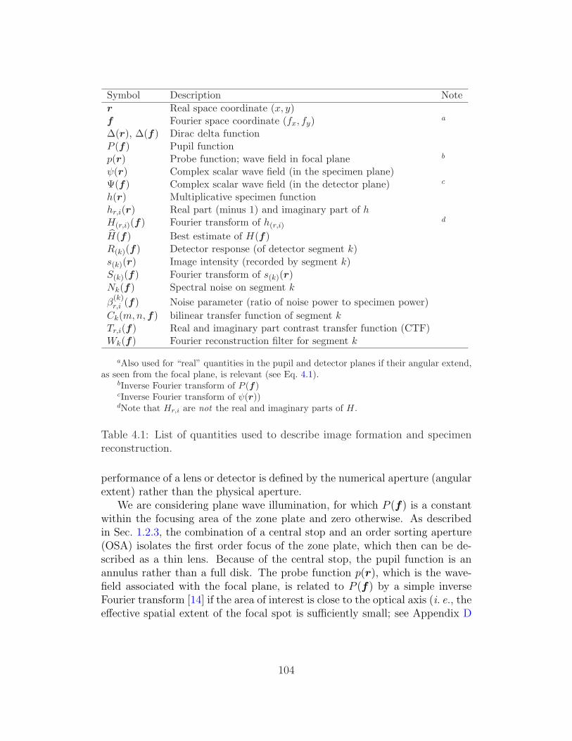
Symbol Description Noter Real space coordinate (x, y)f Fourier space coordinate (fx, fy) a
∆(r), ∆(f) Dirac delta functionP (f) Pupil functionp(r) Probe function; wave field in focal plane b
ψ(r) Complex scalar wave field (in the specimen plane)Ψ(f) Complex scalar wave field (in the detector plane) c
h(r) Multiplicative specimen functionhr,i(r) Real part (minus 1) and imaginary part of hH(r,i)(f) Fourier transform of h(r,i)
d
H(f) Best estimate of H(f)R(k)(f) Detector response (of detector segment k)s(k)(r) Image intensity (recorded by segment k)S(k)(f) Fourier transform of s(k)(r)Nk(f) Spectral noise on segment k
β(k)r,i (f) Noise parameter (ratio of noise power to specimen power)
Ck(m,n, f) bilinear transfer function of segment kTr,i(f) Real and imaginary part contrast transfer function (CTF)Wk(f) Fourier reconstruction filter for segment k
aAlso used for “real” quantities in the pupil and detector planes if their angular extend,as seen from the focal plane, is relevant (see Eq. 4.1).
bInverse Fourier transform of P (f)cInverse Fourier transform of ψ(r))dNote that Hr,i are not the real and imaginary parts of H.
Table 4.1: List of quantities used to describe image formation and specimenreconstruction.
performance of a lens or detector is defined by the numerical aperture (angularextent) rather than the physical aperture.
We are considering plane wave illumination, for which P (f) is a constantwithin the focusing area of the zone plate and zero otherwise. As describedin Sec. 1.2.3, the combination of a central stop and an order sorting aperture(OSA) isolates the first order focus of the zone plate, which then can be de-scribed as a thin lens. Because of the central stop, the pupil function is anannulus rather than a full disk. The probe function p(r), which is the wave-field associated with the focal plane, is related to P (f) by a simple inverseFourier transform [14] if the area of interest is close to the optical axis (i. e., theeffective spatial extent of the focal spot is sufficiently small; see Appendix D
104

zone plate withpupil fn. P(f) OSA
sampleh(r)
probe p(r - r0)
coherentsource
scandisplacement(r
0)
DetectorwithresponsefunctionRk(f)
Detector PlaneIntensity |Ψ(f)|2
FT-1
FT-1
Figure 4.1: Illustration of the imaging process in a scanning transmission x-raymicroscope. A Fresnel zone plate is coherently illuminated. The combinationof a central stop on the zone plate and an order-sorting aperture (OSA) isolatesthe first-order focus, through which the specimen is scanned. The total de-tected intensity gives absorption contrast, but variations in the detector planeintensity distribution |Ψ(f)|2 can be used to extract phase contrast informa-tion.
for details), giving
p(r) =
∫df P (f) exp (+2πi rf) . (4.2)
The specimen is described by a multiplicative complex transmission func-tion h(r) modulating the amplitude and phase of the probing wavefield (seeSec. 1.1.3). If the probe is displaced by a vector r0 with respect to the speci-men,1 we can write
ψ′(r, r0) = p(r − r0) h(r) (4.3)
for the exit wavefield. If the detector is considered to be in the far-field (again,see Appendix D for details), the intensity distribution in the detector plane isgiven by the inverse Fourier transform of the specimen exit wave:
|Ψ(f , r0)|2 =
∣∣∣∣∫
dr p(r − r0) h(r) exp (+2πi r f)
∣∣∣∣2
, (4.4)
where we have dropped all irrelevant phase factors and constants outside theintegral. Using the Fourier shift theorem for p(r − r0) and the convolution
1In STXM, often the specimen is scanned against the fixed probe; we choose to put thedisplacement into the probe function for consistency with other papers on this topic. Inpractice, this choice along with the scan direction determines the orientation of the image.
105

theorem, this is equivalent to
|Ψ(f , r0)|2 = |(P (−f) exp (+2πir0f))⊗f H(−f)|2 , (4.5)
where H(f) is the Fourier transform of the specimen function h(r) and ⊗f
denotes a convolution with respect to f . Feser [20, Sec. 4.3.2] provides a niceillustration of this convolution integral for specimens with only a few discreteFourier components (like a grating). Essentially, each Fourier component inthe specimen gives rise to a diffracted “pupil” in the detector plane, whichinterfere in their overlap region. The scanning process only changes the relativephase of those pupils. For a weak specimen, the zero order pupil will be muchstronger than any higher Fourier component (see below).
The intensity of Eq. 4.4 or 4.5 is then measured by a detector with aresponse function R(f), so that the image recorded by that detector becomes
s(r0) =
∫df R(f) |Ψ(f , r0)|2 . (4.6)
The probe displacement coordinate r0 now turns into the image coordinateas expected. We will study below the images obtained with various detectorconfigurations.
4.1.2 Comparison with the Refraction Model
At this point, it is instructive to compare the result obtained in Eq. 4.4 or 4.5with the simple refraction model used in Chap. 3, which predicts a deflectionof the beam by a certain refraction angle and therefore a shift of the brightfield cone (beam footprint) on the detector. Let us assume a sphere with adiameter of 1.6 µm, a maximum phase shift of 0.5 rad at its center and zeroabsorption as shown in Fig. 4.2. We simulate the sphere being scanned throughan x-ray focus in one dimension across its center. The focus is produced bya zone plate with an outermost zone width of 100 nm (giving a numericalaperture of 6.2 × 10⁻⁴ rad) and a central stop covering 30% of its diameter.The calculations were carried out on a grid of 768 × 768 pixels with a real-space sampling interval of 50 nm. This results in a frequency space samplinginterval of (768× 0.05 µm)−1 = 0.026 µm−1 (see Sec. B.7). The photon energyis assumed to be 10 keV (λ = 0.124 nm).
What would be the beam shift predicted by the refraction model? Thepoint where the sphere is curved by 45 (and the phase shift is 1/
√2 times
the maximum) is at x = 18.6 µm (see Fig. 4.2). The phase gradient dφ/ dxis 0.72 µm−1 at that point. The refraction angle expected from Eq. 3.11 is
106

Y p
ositio
n [
µm
]21
20
19
18
17
X position [µm]2120191817
Scan line
Min = 0.0 (black)
Max = 0.5 (white)1 µm
Ph
ase g
radie
nt
[rad
/µm
]2
1
0
-1
-2
Ph
ase [
rad]
0.6
0.4
0.2
0.0
-0.2
-0.4
-0.6
X position [µm]2120191817
45˚
position
Figure 4.2: Scan line across a phase-shifting sphere. Left: Phase shift of thesimulated sphere, ranging from zero in the background region to 0.5 rad inthe center of the sphere. Right: Profile of the phase shift (solid curve) andthe phase gradient (dashed curve; scale on the right) through the center ofthe sphere. The dotted line marks the position where the sphere is curved by45. In both cases, only the central 4.8 µm wide part of the grid is displayed,whereas the calculations were performed on a (38.4 µm)2 array to achieve finerpixel size in frequency space.
1.4×10⁻⁵ rad or 2.3% of the zone plate opening angle. In frequency coordinates(see Fig. 4.4), this corresponds to a shift by 0.11 µm−1. With the frequencyspace sampling interval noted above, this would correspond to a shift of morethan four pixels and should be clearly noticeable.
We simulate the wave propagation as described in Sec. 4.1.1 and look atthe profile through the detector plane wave field in the x-direction while thesphere is scanned, as illustrated in Fig. 4.3. The resulting plot is shown inFig. 4.4. We can see that the sphere’s phase gradient mostly redistributesintensity within the bright field region (a little bit of radiation is scatteredoutside), rather than shifting the whole beam as predicted by the refractionmodel. However, simulations show that despite this discrepancy, the shift ofthe center of mass of intensity is quite consistent between the refraction modeland the full wave propagation performed here.
As we move further towards the edge of the sphere, the refraction modelreaches its limits, and one might think that this is because of the “infinite”phase gradient. However, consider that in a numerical calculation on a grid ofdiscrete data points, the gradient will never really reach infinity. The conditionrequired, tan θr ¿ 1 and therefore dφ/ dx ¿ k, is not overly restrictive: at E =10 keV, tan θr < 0.1 would allow a phase gradient of up to 5 rad/nm. This is alot compared to total phase shifts on the order of radians for realistic (micron-
107
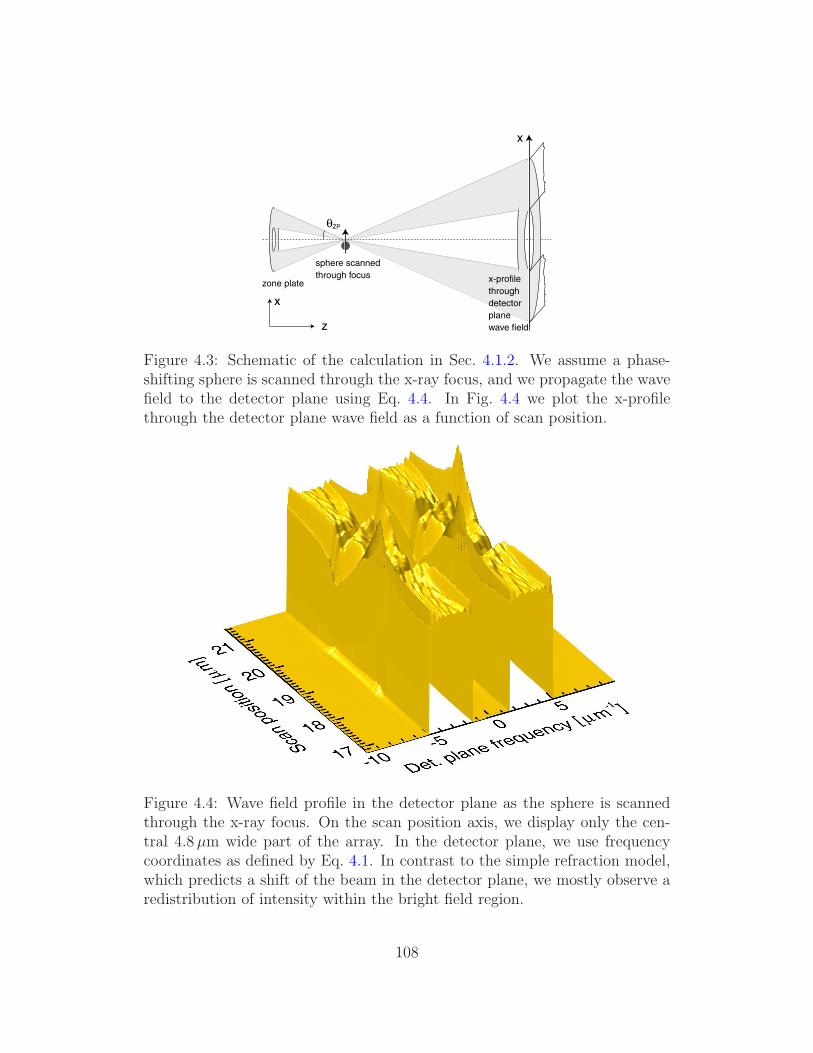
θZP
sphere scanned
through focuszone plate
x
z
x-profile
through
detector
plane
wave field
x
Figure 4.3: Schematic of the calculation in Sec. 4.1.2. We assume a phase-shifting sphere is scanned through the x-ray focus, and we propagate the wavefield to the detector plane using Eq. 4.4. In Fig. 4.4 we plot the x-profilethrough the detector plane wave field as a function of scan position.
Figure 4.4: Wave field profile in the detector plane as the sphere is scannedthrough the x-ray focus. On the scan position axis, we display only the cen-tral 4.8 µm wide part of the array. In the detector plane, we use frequencycoordinates as defined by Eq. 4.1. In contrast to the simple refraction model,which predicts a shift of the beam in the detector plane, we mostly observe aredistribution of intensity within the bright field region.
108

size) objects and pixel sizes on the order of tens of nanometers. The difficultiesrather arise from the fact that the refraction model assumes a constant phasegradient over the probe width, which is often not true any more at the edgeof an object.
4.1.3 Large-area Detector: Incoherent Imaging
Let us now study Eq. 4.6 in more detail and examine the imaging performanceof different detector configurations. First we want to consider a large area(l. a.) detector, which has a uniform intensity response at all frequencies:
Rl. a.(f) = 1. (4.7)
In this case, it is easy to derive from Eq. 4.6 and Eq. 4.4 that the imagerecorded is2
sl. a.(r0) = |p(r)|2 ⊗r |h(r)|2 (4.8)
(see Appendix D for details). In words, the image intensity is given by theintensity distribution of the specimen convolved with the intensity of the probefunction (also called the “intensity point spread function,” see Sec. 1.2.3).This is known as “incoherent imaging” [14, Chap. 6].3 In Fourier space, theconvolution theorem translates this relationship into
Sl. a.(f 0) = MTF(f 0) · H(f 0), (4.9)
where S(f 0) is the Fourier transform of the image s(r0), the modulation trans-fer function MTF is the Fourier transform of the intensity point spread func-tion, and H(f 0) = FT|h(r0)|2 (which is different from |H(f 0)|2!). Thecorrelation theorem will easily prove that the MTF is given by the autocor-relation of the pupil function. It is seen that the incoherent system linearlymaps intensities from the object to the image.
2Strictly speaking, this equation should use the crosscorrelation instead of the convolu-tion. However, in all practical cases, the pupil and therefore the probe will be symmetricalwith respect to the optical axis, so that we can use the convolution instead.
3The zone plate in the STXM still has to be illuminated coherently for diffraction-limitedresolution, but the image obtained with a large area detector is the same as in a full-fieldmicroscope with incoherent illumination.
109
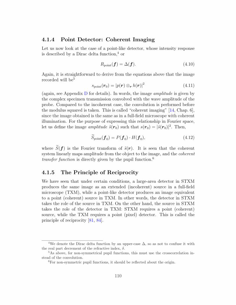
4.1.4 Point Detector: Coherent Imaging
Let us now look at the case of a point-like detector, whose intensity responseis described by a Dirac delta function,4 or
Rpoint(f) = ∆(f). (4.10)
Again, it is straightforward to derive from the equations above that the imagerecorded will be5
spoint(r0) = |p(r)⊗r h(r)|2 (4.11)
(again, see Appendix D for details). In words, the image amplitude is given bythe complex specimen transmission convolved with the wave amplitude of theprobe. Compared to the incoherent case, the convolution is performed beforethe modulus squared is taken. This is called “coherent imaging” [14, Chap. 6],since the image obtained is the same as in a full-field microscope with coherentillumination. For the purpose of expressing this relationship in Fourier space,let us define the image amplitude s(r0) such that s(r0) = |s(r0)|2. Then,
Spoint(f 0) = P (f 0) ·H(f 0), (4.12)
where S(f) is the Fourier transform of s(r). It is seen that the coherentsystem linearly maps amplitude from the object to the image, and the coherenttransfer function is directly given by the pupil function.6
4.1.5 The Principle of Reciprocity
We have seen that under certain conditions, a large-area detector in STXMproduces the same image as an extended (incoherent) source in a full-fieldmicroscope (TXM), while a point-like detector produces an image equivalentto a point (coherent) source in TXM. In other words, the detector in STXMtakes the role of the source in TXM. On the other hand, the source in STXMtakes the role of the detector in TXM: STXM requires a point (coherent)source, while the TXM requires a point (pixel) detector. This is called theprinciple of reciprocity [81, 84].
4We denote the Dirac delta function by an upper-case ∆, so as not to confuse it withthe real part decrement of the refractive index, δ.
5As above, for non-symmetrical pupil functions, this must use the crosscorrelation in-stead of the convolution.
6For non-symmetric pupil functions, it should be reflected about the origin.
110

4.1.6 Segmented Detector: Partially Coherent Imaging
We now want to turn to the case of a segmented detector in STXM to measurethe intensity distribution in the detector plane with separate segments indexedby k, and with individual intensity response functions Rk(f). In analogy tothe above, we call this case partially coherent imaging, and the image signalsk(r0) recorded by segment k is
sk(r0) =
∫df Rk(f) |Ψ(f , r0)|2 , (4.13)
where Rk(f) is set to one within the sensitive area of segment k and zerootherwise.
Expanding |Ψ|2 from Eq. 4.5 into Ψ Ψ∗, we obtain the Fourier transformof the detector images sk(r0) with respect to probe positions r0 as
Sk(f 0) =
∫df Rk(f) (P (−f) · P ∗(−f − f 0))⊗f (H(−f) ·H∗(−f − f 0)) ,
(4.14)for which we first integrated the plane wave factors of the form exp(−2πi r0f)over r0 producing a Dirac delta function, which then permits a second inte-gration (see Appendix D).
For an electromagnetic wave traversing a semi-transparent specimen witha spatially dependent complex index of refraction n(r) = 1− δ(r)− i β(r) andthickness t(r), the multiplicative specimen function can be written as
h(r) = exp[−β(r)k t(r) + i δ(r)k t(r)], (4.15)
where k = 2π/λ (see Sec. 1.1.3). For a weak-amplitude, weak-phase specimen,we can expand to first order:
h(r) = 1 + hr(r) + i hi(r), (4.16)
where the amplitude and phase of the scattered wave
hr(r) = −β(r) k t(r) and
hi(r) = δ(r) k t(r) (4.17)
are small compared to unity. The functions hr,i are real and the Fourier spec-trum of the specimen becomes
H(f) = ∆(f) + Hr(f) + i Hi(f), (4.18)
111

where each summand is the Fourier transform of the corresponding term inEq. 4.167 and ∆(f) is the Dirac-delta function. If terms on the order of |Hr,i|2can be neglected (see Appendix D for details), Eq. 4.14 can be written as
Sk(f 0) = ∆(f 0) Ck(0, 0,f 0) +
+ Hr(f 0) [Ck(−1, 0,f 0) + Ck(0, 1, f 0)]
+ i Hi(f 0) [Ck(−1, 0,f 0)− Ck(0, 1,f 0)] . (4.19)
The functions
Ck(m,n, f 0) =
∫df Rk(f) P (mf 0 − f) P ∗(nf 0 − f) (4.20)
represent bilinear transfer functions [85]. Note that Ck(0, 0, f 0) is constant forall f 0 and represents the intensity measured by detector segment k in absenceof a specimen.
The contrast transfer functions (CTFs) for the real and imaginary part ofthe specimen modulation are identified as
T (k)r (f 0) = Ck(−1, 0,f 0) + Ck(0, 1,f 0)
T(k)i (f 0) = Ck(−1, 0,f 0)− Ck(0, 1, f 0). (4.21)
A measure of the total contrast transfer (including all segments) is [79, Eq. 5.9]
T totr,i (f 0) =
∑
k
∣∣∣T (k)r,i (f 0)
∣∣∣ . (4.22)
T totr,i describes the total spectral power transfer of the imaging system from the
real and imaginary parts of the object to any of the detector images. T totr,i does
not explain the interpretation of recorded images, but is a convenient measurewhen comparing different detector configurations (see Sec. 4.2.5).
4.1.7 Details on the Weak Specimen Approximation
The approximation leading to Eq. 4.19 requires that when expanding (H(−f)·H∗(−f−f 0)) in Eq. 4.14 and using Eq. 4.18 for the specimen function, secondorder terms like |Hr,i|2 can be neglected against terms like ∆(f) · Hr,i(f)(see Appendix D). This is less restrictive than the Taylor expansion of the
7Note that this does not mean that Hr,i(f) are the real and imaginary parts of H(f).
112

exponential specimen function
h(r) = exp(−βkt + iδkt) ≈ 1− βkt + iδkt (4.23)
(which only restricts the absolute values of absorption and phase shift). IfEq. 4.23 is employed, however, the CTFs of Eq. 4.21 can be directly interpretedas amplitude and phase CTFs and Eq. 4.17 is true. In the more general case,amplitude and phase information get partially mixed into the real part hr andimaginary part hi.
Landauer states [79, pg. 37] that the requirements for the weak specimenapproximation are fulfilled if the power of the specimen Fourier transform isconcentrated at the zero frequency, or
∫
f 6=0
df |Hr(f) + i Hi(f)|2 ¿ 1. (4.24)
This condition could be fulfilled for any specimen by embedding it into a largetransparent background and including the background in the reconstruction.However, simulations show that background padding does not affect the valueof the reconstruction. Instead, the weak specimen approximation relies in amore complicated manner on a combination of the specimen spectrum and thepupil function. A more detailed investigation is beyond the scope of this work.
4.2 Calculated Contrast Transfer Functions
The contrast transfer functions of the split, opposite quadrant and first-mo-ment detectors have been published before [46, 49, 86]; here we want to cal-culate the CTFs for the conditions of the simulations and experiments wedescribe below. Note that the CTFs are all zero for segments which are notcovered by the bright field cone (direct beam). This is a consequence of theweak specimen approximation: photons scattered outside the bright field coneare not considered in the imaging process.
4.2.1 Transfer Functions for Soft X-ray Experiments
For the soft x-ray simulations and experiments described in Sec. 4.4, we haveused a Nickel zone plate with a diameter of 80 µm, a central opaque stop witha diameter of 35 µm and an outermost zone width of drN = 30 nm [17]. Thezone plate has a focal length of 1016 µm at the x-ray wavelength λ = 2.36 nm(525 eV photon energy) used.
113

The detector (see Sec. 2.2) has eight sensitive segments as shown in Fig. 2.4.The inner three segments were intended to be used for differential interferencecontrast [54, 55] and break the symmetry of the detector, which is not ideal forthe method described here. One of the new 9 or 10 segment chips (see Fig. 2.4)will also be available for the soft x-ray detector in the future. The separationof the detector from the specimen was chosen such that in spatial frequencyspace the quadrant segments of the detector extend to a normalized spatialfrequency of one. That means, the direct beam projected from the zone plateto the detector just filled the quadrant segments. Fig. 4.5 shows the computerrepresentation of two selected detector segments and the computed CTFs.
4.2.2 Transfer Functions for Medium-Energy Experi-ments
For the medium-energy simulations and experiments described below, we haveused a gold zone plate with a diameter of 160 µm, an outermost zone width of50 nm and a central stop with a diameter of 50 µm. The focal length is 16.1 mmat a wavelength of 0.496 nm (E = 2.5 keV). We used a modified version of thesoft x-ray detector with the 8 segment chip installed (see Fig. 2.4), and thealignment in the z-direction was as above. The CTFs are very similar to theones in the above section, because the only difference is the relative diameterof the central stop. Again, we suffer from the fact that the geometry of the 8segment chip is not ideal for this method; this will become obvious in Sec. 4.5.
4.2.3 Transfer Functions for Hard X-ray Experiments
For the hard x-ray simulations and experiments described below, we haveused a gold zone plate with an effective diameter of 110 µm, a central stopwith a diameter of 45 µm and an effective outermost zone width of 164 nm(see Sec. 4.6.1). The zone plate has a focal length of 14.5 cm for the x-raywavelength λ = 0.124 nm (10 keV photon energy) used.
We have used the segmented hard x-ray detector described in Chap. 2with the 9 segment chip (see Fig. 2.4) installed. The distance of the detectorfrom the specimen was such that the diameter of the beam on the chip wasabout 495 µm (the inner quadrant ring of segments has a diameter of 800 µm).Fig. 4.6 shows the CTFs of one of the inner quadrant segments as well as thetotal transfer of the system. The outer quadrant segments are not interceptedby the bright field cone; therefore, their CTFs are zero.
114

0.00
1.00
0.00
1.00
b) Detector Response
R1(f)
c) Detector Response
R4(f)
0.1*Max
0.1*
Max
0.1
*Max
0.00
1.65
d) Total Real Transfer
Trtot(f)
0.1*Max
0.1*Max
0.1
*Max0.5*
Max
0.00
0.19
e) Real Transfer Tr1(f)
0.1*Max
0.1
*Max
0.1*Max
0.5
*Max
0.00
0.28
f) Real Transfer Tr4(f)
0.1*Max
0.1*
Max
0.1*Max
0.5*Max
0.5*Max
0.5
*Max
0.00
0.57
g) Total Im Transfer Titot(f)
0.5*Max
0.1*Max
0.1*Max
0.1
*Min
0.1*Min
0.5*
Min
-0.10
0.10
h) Imaginary Transfer Ti1(f)
0.5*Max
0.5*
Max
0.1*Max
0.1*
Max
0.1*Min
0.1*Min
0.5*Min
0.5
*Min
-0.14
0.14
i) Imaginary Transfer Ti4(f)
-2 -1 0 1 2
-2
-1
0
1
2no
rmal
ized
spa
tial f
requ
ency
f
y
a) Pupil Function P(f)
normalized spatial frequency fx
0.00
1.00 Detector Segment 1 Detector Segment 4
Figure 4.5: Contrast transfer functions calculated for the conditions of thesoft x-ray experiments: (a) representation of the pupil function; (b, c) detectorresponse of two selected segments; (e, f) real and (h, i) imaginary part transferfunctions of the two segments; (d, g) total real and imaginary transfer of allsegments. Each representation is shown on a normalized frequency scale. Thefrequency with value f = 1 corresponds to the maximum diffraction angle ofthe objective, given by 1/(2 drN). For the zone plate used here (drN = 30 nm)this is f = 16.7 µm−1 so that the above image extends to twice that value or33.3 µm−1. For the imaginary transfer functions, zero response is shown asgrey, and larger positive responses are shown as white while larger negativeresponses are shown as black.
115

-2
-1
0
1
2
0.0
0.2
0.3
0.5
0.7
0.8
1.0
0.0
0.2
0.3
0.5
0.7
0.8
1.0
-2
-1
0
1
2
0.1 * Max
0.0
0.2
0.3
0.5
0.7
0.8
1.0
0.1 * Max
0.5
* M
ax
-0.00
0.04
0.08
0.12
0.17
0.21
0.25
-2 -1 0 1 2
-2
-1
0
1
2
0.1 * Max
0.1 * Max
0.5 * Max
0.5 * Max
0.9 * Max
0.9 * Max
0.00
0.05
0.10
0.15
0.20
0.25
0.30
-2 -1 0 1 2
0.5 * Min
0.1 * Min
0.1
* M
ax
0.5
* M
ax
-0.12
-0.08
-0.04
-0.00
0.04
0.08
0.12
normalized spatial freqency fx
no
rma
lize
d s
pa
tia
l fr
eq
en
cy f
y
(a) Pupil Function P(f) (b) Detector Response R2(f)
(c) Total Real Transfer Trtot(f)
(e) Total Imag Transfer Ti tot(f)
(d) Real Transfer Tr(2)(f)
(f) Real Transfer Ti(2)(f)
Detector Segment 2
Figure 4.6: Contrast transfer functions calculated for the conditions of thehard x-ray experiments: (a) representation of the pupil function; (b) detectorresponse of one selected segment; (d) real and (f) imaginary part transferfunction of the segment; (c, e) total real and imaginary transfer of all segments.See the caption of Fig. 4.5 for a description of the frequency scale. Here,drN = 160 nm, so that fnorm = 2 corresponds to 6.25 µm−1. In this figure, alltransfer function representations (single segment and total) are normalized tothe maximum value of T tot
r for comparison. The contour lines represent 0.1,0.5 and 0.9 of the maximum values each.
116

4.2.4 Contrast Transfer Function Symmetry
It is seen (see Sec. D.2 for more details) that the CTFs for the real part ofthe specimen function are positive and show even symmetry with respect tothe zero spatial frequency (center of the array). Furthermore the CTFs ofopposing detector segments are identical. The CTFs for the imaginary parthave odd symmetry and are opposite in sign for opposing segments.
In the case of incoherent bright field imaging, the signal over the wholedetector plane is summed up. Then, the CTFs for the imaginary part cancelout and only the total CTF for the real part (Figs. 4.5 (d), 4.6 (c)) remains.T tot
r (f) also represents modulation transfer function (MTF, see Sec. 4.1.3) ofthe STXM with a large-area detector. To obtain phase contrast, the emphasisin the past has been on displaying difference images of opposing segments, forwhich only the CTF for the imaginary part gives a contribution. As mentionedin Sec. 1.4 and Chap. 3, the signal in the resulting differential phase contrast(DPC) images is a measure of the specimen phase gradient and shows a di-rectional dependence, which makes interpretation difficult. In Sec. 4.3 we willconsider an approach in which the signals of all detector segments are com-bined in an optimal way and a best estimate of the complex specimen functionis reconstructed by means of Fourier filtering.
4.2.5 Evaluation of Different Detector Geometries
At this point, let us address the question of the best segmentation for optimalphase contrast performance. We have established above that the total transferT tot
r,i is a measure of how much information about the real and imaginary partof the specimen is transferred from the object to the image. Therefore we canuse it to compare different detector geometries. Since the real part transferfunctions T
(k)r are all positive, the total real transfer T tot
r will always be thesame as long as the detector segments together intercept the whole bright fieldcone. As a consequence, the absorption imaging performance depends only onthe characteristics of the zone plate.
In contrast to this, the phase contrast imaging performance clearly de-pends on the detector segmentation in addition to the zone plate. One canwell imagine that a finer segmentation will yield better phase transfer. Fig. 4.7shows five different detector segmentations and the corresponding total imag-inary contrast transfer T tot
i . All of them use the same pupil function, shownas a gray overlay over the detector segmentation. Images (a) and (b) showa simple quadrant geometry and its corresponding contrast transfer. Images(c) and (d) show a double quadrant geometry, and one can see that the finersegmentation in the radial direction leads to better phase transfer in the radial
117

0.0
0.2
0.3
0.5
0.7
0.8
1.0
-2 -1 0 1 2
0.1 * Max
0.5 * Max
0.9 * Max
0.9 * Max
0.00
0.06
0.12
0.18
0.24
0.29
0.35
-2
-1
0
1
2
0.0
0.2
0.3
0.5
0.7
0.8
1.0
-2
-1
0
1
2
0.1 * Max
0.5 * Max
0.5 * Max
0.00
0.06
0.12
0.18
0.24
0.30
0.36
0.0
0.2
0.3
0.5
0.7
0.8
1.0
0.1 * Max
0.5 * Max
0.00
0.06
0.12
0.18
0.24
0.30
0.36
0.0
0.2
0.3
0.5
0.7
0.8
1.0
0.1 * Max
0.5 * Max
0.9
* M
ax
0.00
0.06
0.12
0.18
0.24
0.30
0.36
-2
-1
0
1
2
0.0
0.2
0.3
0.5
0.7
0.8
1.0
-2 -1 0 1 2
-2
-1
0
1
2
0.1 * Max
0.5 * Max
0.00
0.06
0.11
0.17
0.22
0.28
0.33
normalized spatial frequency fx
no
rma
lized s
pa
tial fr
eque
ncy f
y
Dete
cto
r G
eo
me
try
To
tal Im
ag
. C
on
tra
st Tra
nsfe
rD
ete
cto
r G
eo
me
try
To
tal Im
ag
. C
on
tra
st Tra
nsfe
r
(a)
(b)
(i)
(f)(d)
(g)
(e)(c)
(j)(h)
16 x 16 pixel detector
Figure 4.7: Phase contrast transfer comparison of different detector geome-tries. The first and third rows show five different detector segmentations. Thegray overlays show the pupil function on the same frequency scale. The sec-ond and fourth rows show the corresponding total imaginary contrast transferT tot
i . The data values are scaled to the maximum of T totr for comparison. The
contour lines represent 0.1, 0.5 and 0.9 of the maximum level, respectively.
118
direction, in particular at low frequencies. However, the low transfer on thediagonals remains. In Fig. 4.7 (e) and (f), we show an octant geometry andthe corresponding contrast transfer. This time, the finer segmentation in theangular direction leads to a more isotropic response. The geometry shown in(g), where two quadrant structures are rotated by 45 with respect to eachother, combines the advantages of the previous two configurations and offersgood transfer over a large part of the frequency plane, as seen in (h). Images(i) and (j) show, for comparison, a 16 × 16 pixel CCD, and it is apparentthat the phase contrast transfer is not substantially better than for the 8 seg-ment configuration of (h). Therefore, good phase contrast performance can beachieved with a moderate number of segments.
Note that for all configurations, phase contrast transfer goes down to zeroat low spatial frequencies. This is related to the fact that we can measure onlyphase gradients, but not absolute phases (like a constant phase offset acrossthe image).
In practice, additional aspects have to be taken into account. For instance,zone plates are not perfect and might not have an even transmission over thewhole pupil. Instead, their transmission might fall off towards the outside,where the zones become finer and harder to fabricate in perfect quality. Zonesmight even collapse, so that the effective pupil is smaller than the nominalvalue. Or the x-ray beam might not be large enough to fill the zone plateuniformly. Therefore, the intensity distribution of the beam on the detectorchip might be hard to determine. If there is a division between segments inthe radial direction, the contrast transfer functions depend critically on theradial beam intensity distribution relative to the segments as illustrated inFig. 4.8. Note in particular the contrast reversal in the imaginary part CTFsat low frequencies, which is much more pronounced in case A (left; beamevenly distributed over both quadrant rings) than in case B (right; beamconcentrated on the inner ring). Therefore, if the beam intensity distributionon the detector chip is not known well, the result of a phase reconstructionby the method described in Sec. 4.3 might be severely distorted. This willbecome important in Sec. 4.5.
In comparison, the CTFs of a simple quadrant geometry do not depend onthe size of the beam as long as the beam fully stays on the quadrant structure.In certain cases, the simple quadrant structure might thus give better resultsthan a geometry with an additional radial division.
Note that a double-quadrant geometry, where the two quadrant structuresare not rotated with respect to each other (Fig. 4.7 (c)), can always be turnedinto a single quadrant geometry (in software, after data acquisition), so thatthis configuration is a good compromise between practical simplicity and best
119

-2
-1
0
1
2
0.0
0.2
0.3
0.5
0.7
0.8
1.0
-2
-1
0
1
2
0.1 * Max
0.5 *
Max
-0.00
0.02
0.03
0.05
0.06
0.08
0.09
-2
-1
0
1
2
0.5 * Min
0.1 * Min
0.1
* Max
0.5
* M
ax
-0.05
-0.03
-0.02
0.00
0.02
0.03
0.05
-2 -1 0 1 2
-2
-1
0
1
2
0.1 * Max
0.5 * Max
0.00
0.06
0.11
0.17
0.22
0.28
0.33
0.0
0.2
0.3
0.5
0.7
0.8
1.0
0.1 * Max
-0.00
0.04
0.07
0.11
0.15
0.19
0.22
0.1 * Min
0.1 *
Max0.5 * Max
-0.11
-0.07
-0.04
0.00
0.04
0.07
0.11
-2 -1 0 1 2
0.1 * Max
0.5 * Max
0.9 * Max
0.9
* M
ax
0.9
* Max
0.9 * Max
0.00
0.05
0.10
0.15
0.20
0.25
0.30
1 1
normalized spatial frequency fx
no
rma
lize
d s
pa
tia
l fr
eq
ue
ncy f
y
(a) Det Geometry and Pupil A (b) Det Geometry and Pupil B
(c) Real Part CTF Tr1A
(d) Real Part CTF Tr1B
(e) Imag. Part CTF Ti1A (f) Imag. Part CTF Ti
1B
(g) Tot. Imag. CTF Titot, A (h) Tot. Imag. CTF Ti
tot, B
Contrast reversal
at low frequencies
Figure 4.8: Contrast transfer comparison of different detector alignments.Cases A (left) and B (right) use the same detector geometry as shown inthe top row, but the extent of the beam on the detector chip varies as can beseen from the pupil function, shown as a gray overlay on the detector. Detec-tor segment 1 is highlighted in dark gray. Below are shown the real (c, d) andimaginary (e, f) CTFs of segment 1 as well as the total imaginary transfer (g,h) of both detector / pupil configurations. Note the contrast reversal in theimaginary part at low frequencies, much stronger in case A than in case B.
120
contrast transfer.
4.2.6 Fast Computation of Contrast Transfer Functions
It should be pointed out that the bilinear transfer functions Ck(m,n, f) aresimple crosscorrelation integrals, so that they can be computed quickly usingthe convolution theorem as described by Feser [20, Sec. 4.3.3].
4.3 Fourier Filter Reconstruction
Now that we have described how images are formed in a scanning microscopewith a segmented detector, can we invert the process and determine the com-plex specimen function (amplitude and phase) from the images obtained? Onecan optimally combine the images recorded on all segments of the detector toreconstruct an estimate of the specimen function in the presence of noise. Weare following the approach of McCallum, Landauer and Rodenburg ([76–79];see Appendix D for details) developed for scanning electron microscopy, whilewe focus here on a truly quantitative reconstruction of the specimen func-tion (see Eq. 4.16) and the treatment of the measurement noise. The methodis closely related to the Wiener filter (see Appendix C) commonly used fortransfer function deconvolution in signal and image processing.
4.3.1 Derivation of the Reconstruction Formula
We assume that an estimate of the specimen Fourier transform H(f) can beformed as a filtered sum of the detector images Sk(f) (see Eq. 4.19) in Fourierspace, or
H(f) =∑
k
Wk(f) Sk(f), (4.25)
where Wk(f) represent Fourier filter weighting functions. The root meansquare (rms) error of the reconstruction can be defined as
ε =
∫df
⟨∣∣∣H(f)−H(f)∣∣∣2⟩
, (4.26)
which has to be minimized for an optimal reconstruction. The brackets 〈〉indicate an expectation value, which averages over many measurements of thenoisy data Sk. Since the integrand of Eq. 4.26 is real and greater than or equalto zero for all spatial frequencies f , the minimization of ε can be performed
121

for each value of f independently and we can omit the explicit dependence onf and the integration in the following.
The minimal reconstruction error is found by setting the partial derivativeof the integrand with respect to the weighting functions Wk to zero, which canbe written as (see Appendix D)
⟨S∗k
(∑
l
Wl Sl −H
)⟩= 0. (4.27)
This constitutes a linear set of equations for the Wk, which can be solved forall Wk [77, 78], if we substitute for the Fourier transformed detector imagesSk(f) the weak specimen approximation from Eq. 4.19:
Sk(f) = Hr(f) T (k)r (f) + i Hi(f) T
(k)i (f) + Nk(f) for f 6= 0, (4.28)
where Nk(f) is added as the spectral noise of detector segment k. The ∆(f)-term in Eq. 4.19, which represents the DC or background level of the image,is omitted here but will be taken into account below. The general solution,which is given in Eq. D.69, can be further simplified [78] if the pupil functionP (f) is real and centrosymmetric and each detector segment k has a corre-sponding opposing segment k such that Rk(f) = Rk(−f). In this case, thereconstruction filters are given by
Wk(f) =T
(k)∗r (f)
∑l
∣∣∣T (l)r (f)
∣∣∣2
+ βr(f)+
T(k)∗i (f)
∑l
∣∣∣T (l)i (f)
∣∣∣2
+ βi(f)for f 6= 0, (4.29)
where T(k)r,i (f) are the CTFs for the real and imaginary part (see Eq. 4.21),
and the noise terms βr,i(f) are defined as
β(k)r,i (f) =
〈|Nk(f)|2〉|Hr,i(f)|2 . (4.30)
For Eq. 4.29 to be valid, the noise power has to be equal for all detectorsegments (β
(k)r,i (f) = βr,i(f) for all k).
For the zero frequency component, we assume that the noise contributionis negligible (i. e., the noise has an average close to zero) and that Hr(f =0)is small compared to the Dirac ∆-term in Eq. 4.18 (weak specimen). Keeping
in mind that T(k)r (f) = 2 Ck(0, 0,f) and T
(k)i (f) = 0 for f = 0, it can then
be shown (see Appendix D) that the reconstruction filter is given by Eq. 4.29
122

multiplied by two, or
Wk(0) =2 T
(k)∗r (0)
∑l
∣∣∣T (l)r (0)
∣∣∣2
+ βr(0). (4.31)
After calculating the reconstruction filters (see Sec. 4.3.2), the specimen func-tion (Eq. 4.15) can then be obtained from Eq. 4.25 and an inverse Fouriertransform.
For a quantitative reconstruction, attention must be paid to the scale of thepupil function (which determines the numerical value of the transfer functions).The integral of the squared “true” pupil function (in the experiment) is equalto the number of incident photons, which can only be estimated from thefinal images. Therefore, it is better to use an arbitrarily scaled pupil for thecalculation of the transfer functions and reconstruct the specimen as describedabove. Then, one can define a background region (see Fig. 4.12) and normalizethe reconstructed specimen by the complex mean of that region, so that thebackground becomes transparent (i. e., has a numerical value of one) and hasa phase shift of zero.
The terms β(k)r,i explicitly depend on the ratio of noise to specimen power,
which varies depending on the signal strength and specimen properties. There-fore it is not possible to calculate general reconstruction filters to be used withevery measurement. As is commonly done in Wiener filtering, one can use aconstant value of βr,i for all frequencies and adjust it interactively to obtainthe “visually best” result for the reconstruction [87]. However, it is usuallybetter to estimate the required quantities from the measurement itself as isdemonstrated below.
The fact that this reconstruction method processes information up to twicethe frequency cutoff of the zone plate lens might lead to the conclusion thata factor of two in resolution is gained, and in fact, Landauer et al. [76] callthe method “double resolution imaging” (compared to coherent imaging withan on-axis point detector). Note, however, that the unprocessed incoherentbright field and differential phase contrast images each contain information upto twice the zone plate cutoff frequency, albeit at less contrast (see Figs. 4.5 (d)and (g); 4.6 (c) and (e)). Moreover, the cutoff frequency alone does not suf-ficiently describe resolution and image quality, as described in Chap. 6.5 ofGoodman [14].
123
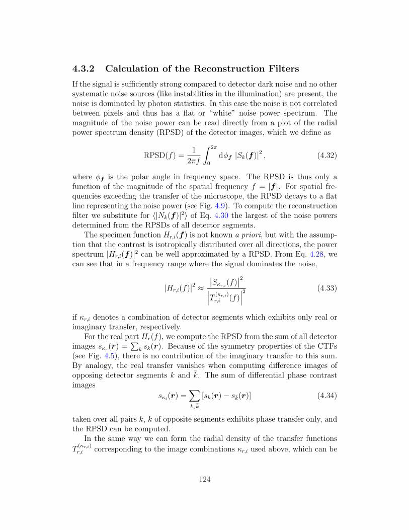
4.3.2 Calculation of the Reconstruction Filters
If the signal is sufficiently strong compared to detector dark noise and no othersystematic noise sources (like instabilities in the illumination) are present, thenoise is dominated by photon statistics. In this case the noise is not correlatedbetween pixels and thus has a flat or “white” noise power spectrum. Themagnitude of the noise power can be read directly from a plot of the radialpower spectrum density (RPSD) of the detector images, which we define as
RPSD(f) =1
2πf
∫ 2π
0
dφf |Sk(f)|2 , (4.32)
where φf is the polar angle in frequency space. The RPSD is thus only afunction of the magnitude of the spatial frequency f = |f |. For spatial fre-quencies exceeding the transfer of the microscope, the RPSD decays to a flatline representing the noise power (see Fig. 4.9). To compute the reconstructionfilter we substitute for 〈|Nk(f)|2〉 of Eq. 4.30 the largest of the noise powersdetermined from the RPSDs of all detector segments.
The specimen function Hr,i(f) is not known a priori, but with the assump-tion that the contrast is isotropically distributed over all directions, the powerspectrum |Hr,i(f)|2 can be well approximated by a RPSD. From Eq. 4.28, wecan see that in a frequency range where the signal dominates the noise,
|Hr,i(f)|2 ≈∣∣Sκr,i
(f)∣∣2
∣∣∣T (κr,i)r,i (f)
∣∣∣2 (4.33)
if κr,i denotes a combination of detector segments which exhibits only real orimaginary transfer, respectively.
For the real part Hr(f), we compute the RPSD from the sum of all detectorimages sκr(r) =
∑k sk(r). Because of the symmetry properties of the CTFs
(see Fig. 4.5), there is no contribution of the imaginary transfer to this sum.By analogy, the real transfer vanishes when computing difference images ofopposing detector segments k and k. The sum of differential phase contrastimages
sκi(r) =
∑
k, k
[sk(r)− sk(r)] (4.34)
taken over all pairs k, k of opposite segments exhibits phase transfer only, andthe RPSD can be computed.
In the same way we can form the radial density of the transfer functions
T(κr,i)r,i corresponding to the image combinations κr,i used above, which can be
124

Rad
ial P
ower
Spe
ctru
m D
ensi
ty [p
h2 ]
105
104
103
102
101
100
10-1
10-2
Spatial Frequency [µm-1]100.010.01.00.1
limit = 33.3 µm-1
Information
Noise level
Estimation of Specimen Power Spectrum
Imag. part piecewise power law fitReal part piecewise power law fitImag. part transfer-correctedReal part transfer-correctedImaginary partReal part
Figure 4.9: Radial power spectrum densities extracted from the images of theweak Siemens star pattern simulated in Sec. 4.4.1. Beyond the informationlimit of the objective zone plate 1/drN = 33.3 µm−1, the power spectrumdecays to a flat line representing the noise level. The actual RPSD of thesimulated specimen (not shown), if properly scaled by the square of the numberof photons, coincides perfectly with the transfer-corrected real part RPSDexcept at the highest frequencies. The transfer-corrected imaginary part istoo large at low frequencies due to the low value of the transfer functions.
used to correct the signal-RPSDs to obtain estimates of the real and imaginaryspecimen power spectra according to Eq. 4.33.
Figure 4.9 shows signal and transfer-corrected RPSDs of the weak Siemensstar test pattern simulated in Sec. 4.4.1. As the specimen power gets lower thanthe noise power, the corrected RPSDs lose their meaning and curve steeplyupward. For most specimens, the decline of the signal with frequency is wellapproximated by a power law (represented by a straight line on a log-log scale).Therefore, a power law fit to the corrected RPSDs can be made in the mediumspatial frequency range, which is used as the input |Hr,i|2 of Eq. 4.30. The testpattern used in the following simulations and experiments, however, peaks inthe medium frequency range so that we chose to do a piecewise power law fitinstead.
125
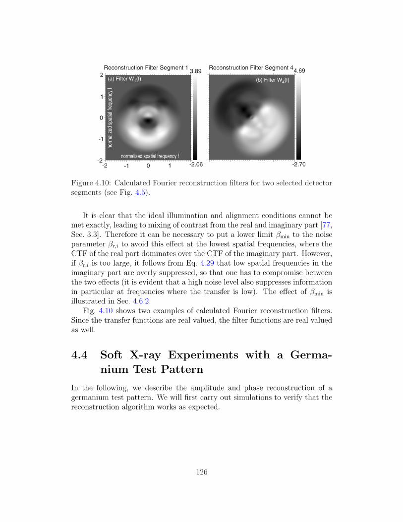
-2 -1 0 1-2
-1
0
1
23.89
-2.06
(a) Filter W1(f)
norm
aliz
ed s
patia
l fre
quen
cy f
normalized spatial frequency f
Reconstruction Filter Segment 14.69
-2.70
Reconstruction Filter Segment 4
(b) Filter W4(f)
Figure 4.10: Calculated Fourier reconstruction filters for two selected detectorsegments (see Fig. 4.5).
It is clear that the ideal illumination and alignment conditions cannot bemet exactly, leading to mixing of contrast from the real and imaginary part [77,Sec. 3.3]. Therefore it can be necessary to put a lower limit βmin to the noiseparameter βr,i to avoid this effect at the lowest spatial frequencies, where theCTF of the real part dominates over the CTF of the imaginary part. However,if βr,i is too large, it follows from Eq. 4.29 that low spatial frequencies in theimaginary part are overly suppressed, so that one has to compromise betweenthe two effects (it is evident that a high noise level also suppresses informationin particular at frequencies where the transfer is low). The effect of βmin isillustrated in Sec. 4.6.2.
Fig. 4.10 shows two examples of calculated Fourier reconstruction filters.Since the transfer functions are real valued, the filter functions are real valuedas well.
4.4 Soft X-ray Experiments with a Germa-
nium Test Pattern
In the following, we describe the amplitude and phase reconstruction of agermanium test pattern. We will first carry out simulations to verify that thereconstruction algorithm works as expected.
126
1 µm
Figure 4.11: Simulated incoherent bright field (left) and differential phasecontrast (DPC, right) image of the weak Siemens star specimen. The insetshows the detector segments contributing to the image (green: added; red:subtracted; gray: not used). The line profile in the absorption image (aver-aged over three lines) shows how finer features have less contrast despite theconstant thickness of the original specimen. In the DPC image, it can be seenthat the contrast is strongest for features perpendicular to the direction ofdifferentiation, and declines to zero for features parallel to that direction.
4.4.1 Simulations
We have simulated the imaging and reconstruction process for a Siemensstar test pattern in conditions close to those of the experiments describedin Sec. 4.4.2. The parameters of the zone plate and the detector have beenspecified in Sec. 4.2.1, where we have already computed the corresponding con-trast transfer functions. In a first simulation, the spokes of the test pattern areassumed to have both an amplitude βkt and a phase shift δkt of 0.1 to fulfillthe weak specimen approximation. However, the method will be most benefi-cial in cases where the phase shift contribution is larger than the absorption,and since the actual test pattern used in Sec. 4.4.2 has an estimated amplitudeof 0.41 and phase of 1.14 in the spokes, we have repeated the simulation withthose values as well (strong specimen). The background has been set to betransparent in all cases. All calculations have been carried out on a grid of256× 256 pixels with an assumed real space sampling interval of 15 nm. Theincident intensity has been assumed to be 7000 photons per scan pixel, andrandom Poisson-distributed noise has been applied to the resulting image ofeach detector segment. For the simulation of the imaging process, the formulafor general specimens (Eq. 4.13) has been used.
Fig. 4.11 shows the simulated incoherent bright field and differential phase
127
contrast images of the weak specimen. The incoherent bright field (absorption)image is often used to extract the optical density OD = µt of a feature (seeSec. 1.3.2). From Eq. 1.16, we see that OD/2 = βkt. In our case, we can use theoptical density to obtain an independent measure of the specimen absorptionβkt for comparison with the result of the reconstruction. However, it turnsout that the optical density underestimates βkt considerably even if I and I0
are determined from the wider features of the test pattern (see Table 4.2). Thereason is the decline of the amplitude transfer function at higher frequenciescorresponding to finer features in the specimen (see Fig. 4.5 (d)). In otherwords, the concept of optical density assumes a perfect projection image anddoes not take into account the finite extent of the probe function due to thelimited numerical aperture of the zone plate. Even if the probe is centeredon a spoke, part of the wavefield is incident in the background region andtherefore not attenuated, so that the intensity measured for that scan pixel ishigher than expected. This effect is particularly pronounced for an object withsharp edges like the test pattern and gets stronger with decreasing feature size,which is evident from the line profile shown in Fig. 4.11. Since the Fourier filterreconstruction method corrects for the frequency transfer of the optical system,we expect that effect to be absent in the final result; the reconstructed βktof the spokes should be larger than the one obtained from the optical densityand independent of spoke width.
Before reconstruction, the edges of the images have been smoothed with aGaussian window function of 5 pixels width to avoid the edge effects due todiscontinuities inherent in discrete Fourier transforms. The transfer functionsand reconstruction filters have been calculated as described in Sec. 4.2.1 and4.3.2. The lower limit βmin of the noise parameter was chosen to be 10−4.
The reconstructed specimen is shown for the weak case in Fig. 4.12. Thevisual appearance is very similar, albeit less noisy (because of the strongercontrast), for the strong specimen. It can be seen from the line profile thatthe spokes are reconstructed with almost constant thickness independent ofwidth (the decline towards the edge is due to the Gaussian smoothing).
A region has been selected in the spoke (bright) areas, whose mean valueis evaluated as a measure for the numerical value of the reconstruction. Theresults are shown in Table 4.2. For the weak specimen, there is very goodagreement between the original and reconstructed amplitude and phase. Inthe case of the strong specimen, the reconstructed values are considerablylower as a consequence of the violation of the weak specimen approximation.
128

0.12 0.10 0.08 0.06 0.04 0.02 0.00 -0.0 2
Amplitude attenuation β kt
0.10 0.05 0.00
Phase advance δ kt
1 1
2 2
Figure 4.12: Reconstructed amplitude attenuation and phase advance of thesimulated weak specimen. Shown in the upper right are the selected back-ground region (1) used to normalize the reconstruction and the feature region(2) whose mean value has been determined as a measure for the numericalvalue of the reconstruction.
weak specimen strong specimensimul. OD/2 recon. simul. OD/2 recon.
βkt 0.100 0.087 0.098 0.410 0.355 0.349δkt 0.100 0.103 1.14 0.896
Table 4.2: Simulated and reconstructed values of the amplitude attenuationβkt and phase advance δkt of the weak and strong Siemens star pattern. OD isthe optical density (see text) and was determined from the incoherent brightfield image (the same feature and background regions which are shown inFig. 4.12 were used).
129

1 µm
Figure 4.13: Incoherent bright field (left) and differential phase contrast (DPC,right) images of the germanium test pattern.
4.4.2 Experimental Results
We have imaged a Siemens-star test pattern in germanium fabricated by elec-tron beam lithography [88]. A scan with 400 × 400 pixels and a pixel size of15 nm has been collected (data taken by Michael Feser) at a photon energy of525 eV at the NSLS STXM (see Sec. 1.2.4). The properties of the zone plateand the detector are as described in Sec. 4.2.1. The total incident intensity wasabout 7000 photons per scan pixel, ranging from about 500 to 1200 photonsfor the different detector segments. Fig. 4.13 shows the incoherent bright fieldimage and a DPC image.
The thickness of the spokes is not known very well. The absorption βktestimated as half the optical density of the large germanium features, as wasdone in Sec. 4.4.1, is about 0.36, which would evaluate to a thickness of about150 nm using the tabulated data of Henke et al. [9]. However, as describedabove, this method tends to underestimate the thickness, and in fact an as-sumed βkt of 0.41 in the simulations resulted in OD/2 ≈ 0.36 (see Table 4.2).Therefore, we assume that the actual germanium test pattern is closer to thatvalue, which would mean a thickness of about 170 nm and an estimated phaseshift δkt of 1.14 rad.
The edges of the scan have been smoothed as before with a Gaussian win-dow function of 5 pixels width before Fourier filtering. The radial power spec-trum densities used to estimate the noise parameters βr,i are shown in Fig. 4.14.The specimen phase advance δkt and absorptive component βkt are extractedfrom the resulting estimate of the complex specimen transmission functionafter filtering and normalizing (Fig. 4.15).
130

Rad
ial P
ower
Spe
ctru
m D
ensi
ty [p
h2 ]
104
102
100
10-2
10-4
Spatial Frequency [µm-1]100.010.01.00.1
Estimation of Specimen Power Spectrum
Imag. part piecewise power law fit
Real part piecewise power law fit
Imag. part transfer-corrected
Real part transfer-corrected
Imaginary part
Real part
Figure 4.14: Radial power spectrum densities used to estimate the specimenpower spectrum of the germanium test pattern.
131
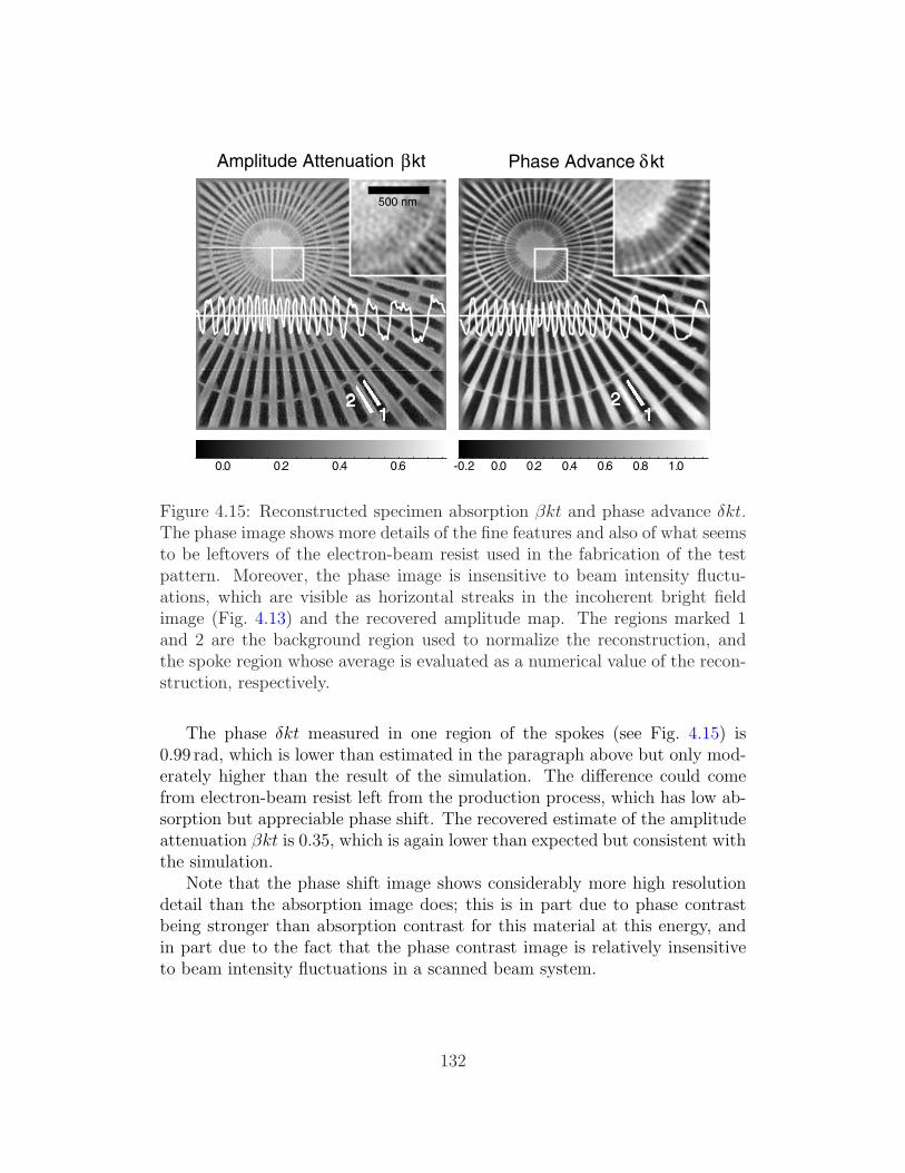
0.60.40.20.0
Amplitude Attenuation βkt
1.00.80.60.40.20.0-0.2
Phase Advance δkt
500 nm
2 211
Figure 4.15: Reconstructed specimen absorption βkt and phase advance δkt.The phase image shows more details of the fine features and also of what seemsto be leftovers of the electron-beam resist used in the fabrication of the testpattern. Moreover, the phase image is insensitive to beam intensity fluctu-ations, which are visible as horizontal streaks in the incoherent bright fieldimage (Fig. 4.13) and the recovered amplitude map. The regions marked 1and 2 are the background region used to normalize the reconstruction, andthe spoke region whose average is evaluated as a numerical value of the recon-struction, respectively.
The phase δkt measured in one region of the spokes (see Fig. 4.15) is0.99 rad, which is lower than estimated in the paragraph above but only mod-erately higher than the result of the simulation. The difference could comefrom electron-beam resist left from the production process, which has low ab-sorption but appreciable phase shift. The recovered estimate of the amplitudeattenuation βkt is 0.35, which is again lower than expected but consistent withthe simulation.
Note that the phase shift image shows considerably more high resolutiondetail than the absorption image does; this is in part due to phase contrastbeing stronger than absorption contrast for this material at this energy, andin part due to the fact that the phase contrast image is relatively insensitiveto beam intensity fluctuations in a scanned beam system.
132
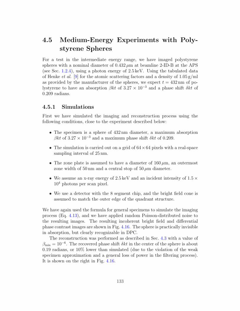
4.5 Medium-Energy Experiments with Poly-
styrene Spheres
For a test in the intermediate energy range, we have imaged polystyrenespheres with a nominal diameter of 0.432 µm at beamline 2-ID-B at the APS(see Sec. 1.2.4), using a photon energy of 2.5 keV. Using the tabulated dataof Henke et al. [9] for the atomic scattering factors and a density of 1.05 g/mlas provided by the manufacturer of the spheres, we expect t = 432 nm of po-lystyrene to have an absorption βkt of 3.27 × 10⁻³ and a phase shift δkt of0.209 radians.
4.5.1 Simulations
First we have simulated the imaging and reconstruction process using thefollowing conditions, close to the experiment described below:
• The specimen is a sphere of 432 nm diameter, a maximum absorptionβkt of 3.27× 10⁻³ and a maximum phase shift δkt of 0.209.
• The simulation is carried out on a grid of 64×64 pixels with a real-spacesampling interval of 25 nm.
• The zone plate is assumed to have a diameter of 160 µm, an outermostzone width of 50 nm and a central stop of 50 µm diameter.
• We assume an x-ray energy of 2.5 keV and an incident intensity of 1.5×10⁴ photons per scan pixel.
• We use a detector with the 8 segment chip, and the bright field cone isassumed to match the outer edge of the quadrant structure.
We have again used the formula for general specimens to simulate the imagingprocess (Eq. 4.13), and we have applied random Poisson-distributed noise tothe resulting images. The resulting incoherent bright field and differentialphase contrast images are shown in Fig. 4.16. The sphere is practically invisiblein absorption, but clearly recognizable in DPC.
The reconstruction was performed as described in Sec. 4.3 with a value ofβmin = 10−6. The recovered phase shift δkt in the center of the sphere is about0.19 radians, or 10% lower than simulated (due to the violation of the weakspecimen approximation and a general loss of power in the filtering process).It is shown on the right in Fig. 4.16.
133
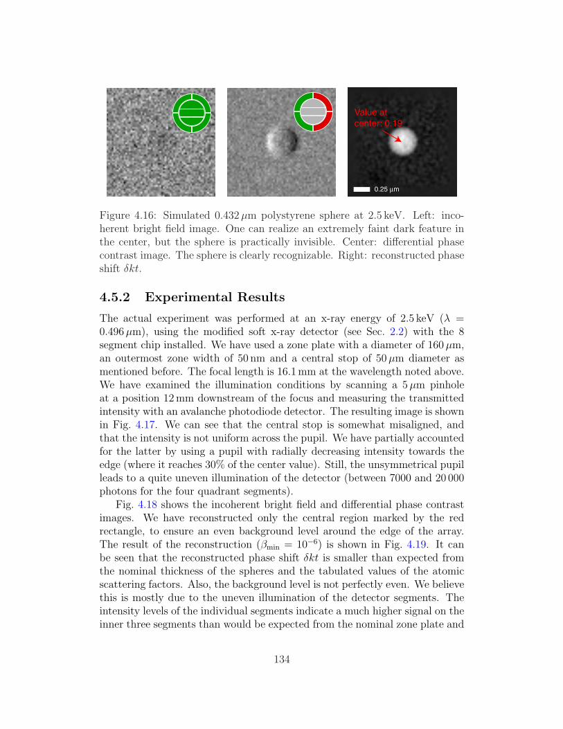
0.25 µm
Value at
center: 0.19
Figure 4.16: Simulated 0.432 µm polystyrene sphere at 2.5 keV. Left: inco-herent bright field image. One can realize an extremely faint dark feature inthe center, but the sphere is practically invisible. Center: differential phasecontrast image. The sphere is clearly recognizable. Right: reconstructed phaseshift δkt.
4.5.2 Experimental Results
The actual experiment was performed at an x-ray energy of 2.5 keV (λ =0.496 µm), using the modified soft x-ray detector (see Sec. 2.2) with the 8segment chip installed. We have used a zone plate with a diameter of 160 µm,an outermost zone width of 50 nm and a central stop of 50 µm diameter asmentioned before. The focal length is 16.1 mm at the wavelength noted above.We have examined the illumination conditions by scanning a 5 µm pinholeat a position 12 mm downstream of the focus and measuring the transmittedintensity with an avalanche photodiode detector. The resulting image is shownin Fig. 4.17. We can see that the central stop is somewhat misaligned, andthat the intensity is not uniform across the pupil. We have partially accountedfor the latter by using a pupil with radially decreasing intensity towards theedge (where it reaches 30% of the center value). Still, the unsymmetrical pupilleads to a quite uneven illumination of the detector (between 7000 and 20 000photons for the four quadrant segments).
Fig. 4.18 shows the incoherent bright field and differential phase contrastimages. We have reconstructed only the central region marked by the redrectangle, to ensure an even background level around the edge of the array.The result of the reconstruction (βmin = 10−6) is shown in Fig. 4.19. It canbe seen that the reconstructed phase shift δkt is smaller than expected fromthe nominal thickness of the spheres and the tabulated values of the atomicscattering factors. Also, the background level is not perfectly even. We believethis is mostly due to the uneven illumination of the detector segments. Theintensity levels of the individual segments indicate a much higher signal on theinner three segments than would be expected from the nominal zone plate and
134
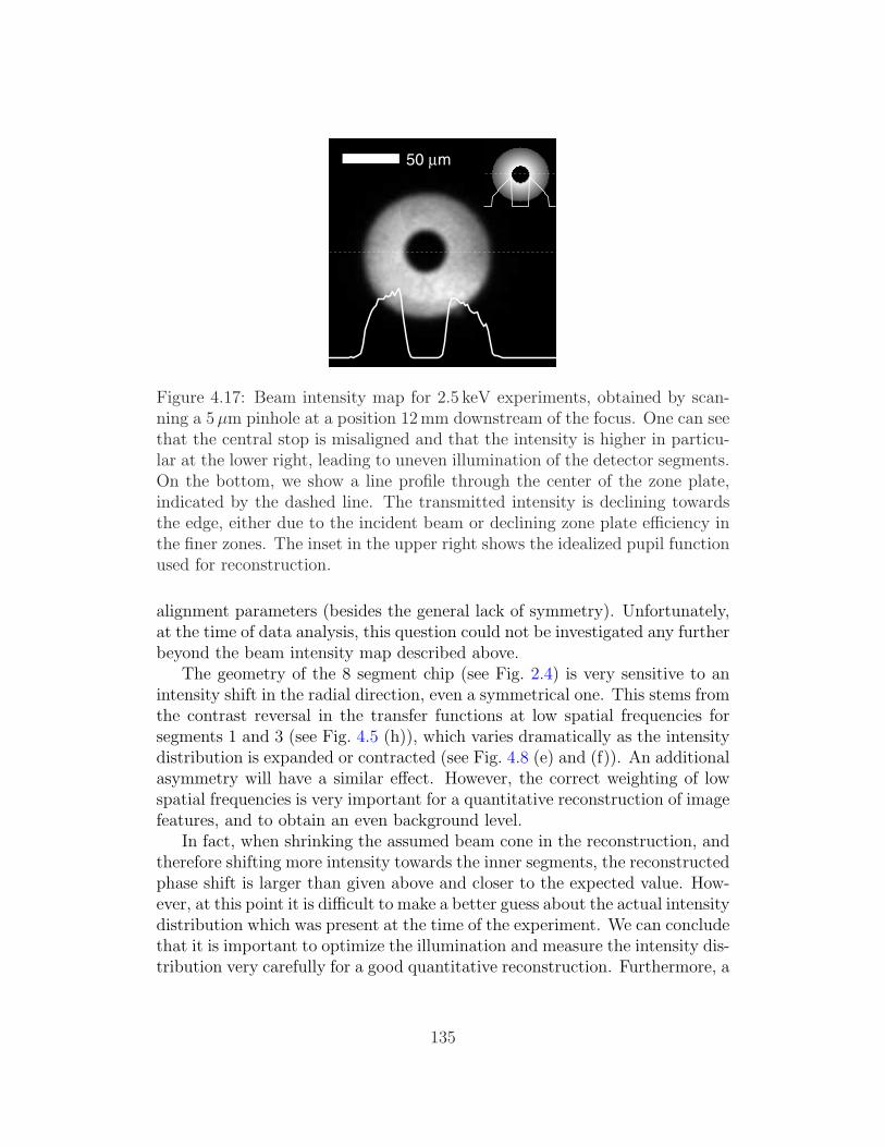
50 µm
Figure 4.17: Beam intensity map for 2.5 keV experiments, obtained by scan-ning a 5 µm pinhole at a position 12 mm downstream of the focus. One can seethat the central stop is misaligned and that the intensity is higher in particu-lar at the lower right, leading to uneven illumination of the detector segments.On the bottom, we show a line profile through the center of the zone plate,indicated by the dashed line. The transmitted intensity is declining towardsthe edge, either due to the incident beam or declining zone plate efficiency inthe finer zones. The inset in the upper right shows the idealized pupil functionused for reconstruction.
alignment parameters (besides the general lack of symmetry). Unfortunately,at the time of data analysis, this question could not be investigated any furtherbeyond the beam intensity map described above.
The geometry of the 8 segment chip (see Fig. 2.4) is very sensitive to anintensity shift in the radial direction, even a symmetrical one. This stems fromthe contrast reversal in the transfer functions at low spatial frequencies forsegments 1 and 3 (see Fig. 4.5 (h)), which varies dramatically as the intensitydistribution is expanded or contracted (see Fig. 4.8 (e) and (f)). An additionalasymmetry will have a similar effect. However, the correct weighting of lowspatial frequencies is very important for a quantitative reconstruction of imagefeatures, and to obtain an even background level.
In fact, when shrinking the assumed beam cone in the reconstruction, andtherefore shifting more intensity towards the inner segments, the reconstructedphase shift is larger than given above and closer to the expected value. How-ever, at this point it is difficult to make a better guess about the actual intensitydistribution which was present at the time of the experiment. We can concludethat it is important to optimize the illumination and measure the intensity dis-tribution very carefully for a good quantitative reconstruction. Furthermore, a
135
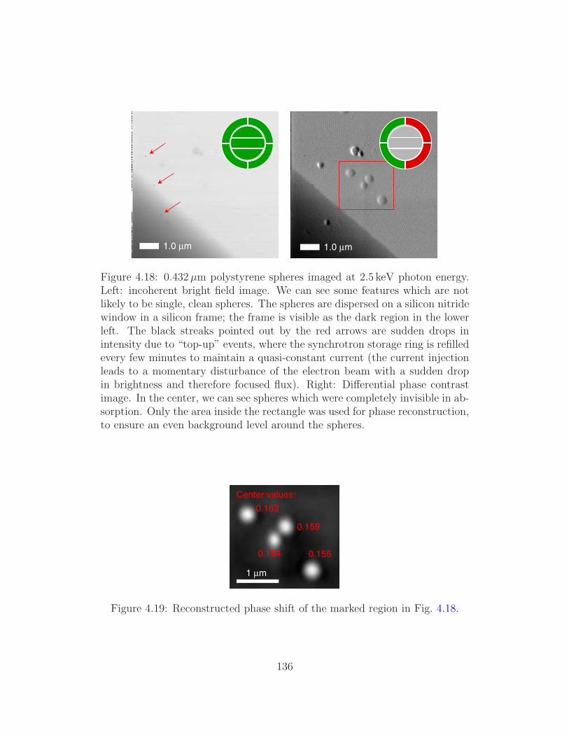
1.0 µm 1.0 µm
Figure 4.18: 0.432 µm polystyrene spheres imaged at 2.5 keV photon energy.Left: incoherent bright field image. We can see some features which are notlikely to be single, clean spheres. The spheres are dispersed on a silicon nitridewindow in a silicon frame; the frame is visible as the dark region in the lowerleft. The black streaks pointed out by the red arrows are sudden drops inintensity due to “top-up” events, where the synchrotron storage ring is refilledevery few minutes to maintain a quasi-constant current (the current injectionleads to a momentary disturbance of the electron beam with a sudden dropin brightness and therefore focused flux). Right: Differential phase contrastimage. In the center, we can see spheres which were completely invisible in ab-sorption. Only the area inside the rectangle was used for phase reconstruction,to ensure an even background level around the spheres.
1 µm
0.163
0.154
0.159
0.155
Center values:
Figure 4.19: Reconstructed phase shift of the marked region in Fig. 4.18.
136
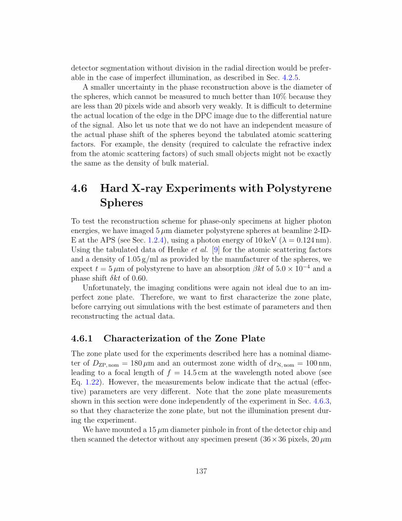
detector segmentation without division in the radial direction would be prefer-able in the case of imperfect illumination, as described in Sec. 4.2.5.
A smaller uncertainty in the phase reconstruction above is the diameter ofthe spheres, which cannot be measured to much better than 10% because theyare less than 20 pixels wide and absorb very weakly. It is difficult to determinethe actual location of the edge in the DPC image due to the differential natureof the signal. Also let us note that we do not have an independent measure ofthe actual phase shift of the spheres beyond the tabulated atomic scatteringfactors. For example, the density (required to calculate the refractive indexfrom the atomic scattering factors) of such small objects might not be exactlythe same as the density of bulk material.
4.6 Hard X-ray Experiments with Polystyrene
Spheres
To test the reconstruction scheme for phase-only specimens at higher photonenergies, we have imaged 5 µm diameter polystyrene spheres at beamline 2-ID-E at the APS (see Sec. 1.2.4), using a photon energy of 10 keV (λ = 0.124 nm).Using the tabulated data of Henke et al. [9] for the atomic scattering factorsand a density of 1.05 g/ml as provided by the manufacturer of the spheres, weexpect t = 5 µm of polystyrene to have an absorption βkt of 5.0× 10⁻⁴ and aphase shift δkt of 0.60.
Unfortunately, the imaging conditions were again not ideal due to an im-perfect zone plate. Therefore, we want to first characterize the zone plate,before carrying out simulations with the best estimate of parameters and thenreconstructing the actual data.
4.6.1 Characterization of the Zone Plate
The zone plate used for the experiments described here has a nominal diame-ter of DZP, nom = 180 µm and an outermost zone width of drN, nom = 100 nm,leading to a focal length of f = 14.5 cm at the wavelength noted above (seeEq. 1.22). However, the measurements below indicate that the actual (effec-tive) parameters are very different. Note that the zone plate measurementsshown in this section were done independently of the experiment in Sec. 4.6.3,so that they characterize the zone plate, but not the illumination present dur-ing the experiment.
We have mounted a 15 µm diameter pinhole in front of the detector chip andthen scanned the detector without any specimen present (36×36 pixels, 20 µm
137

100 µm
495 µm
195 µm
(a)
zone plate detector
DZ
P
Dsto
p
DZ
P'
Dsto
p'
f = 14.5 cm f' = 66.5 cm
(b)
Figure 4.20: (a) Intensity map of the beam, obtained by scanning the detector(apertured with a 5 µm pinhole) in the detector plane. Shown is the sum ofdetector segments 1 and 3 (of the 9 segment chip), since the pinhole happenedto be placed over those two segments. The red arrows highlight faint featuresvisible on a circle corresponding to the nominal zone plate diameter. (b)Schematic of the measurement geometry.
steps). This gives an intensity map in the detector plane, which is a projectionof the zone plate transmittance. A central stop of Dstop = 45 µm diameter hasbeen installed as in regular microprobe operation. The distance from the focusto the detector has been measured to be f ′ = 66.5 cm. The resulting imageis shown in Fig. 4.20 (a). Measuring the projected stop diameter D′
stop fromthe image and referring to the geometry illustrated in Fig. 4.20 (b), we candetermine the actual stop diameter if we use the focal length obtained fromthe nominal zone plate parameters:
Dstop =f
f ′·D′
stop =14.5 cm
66.5 cm· 195 µm = 42.5 µm, (4.35)
which is in good agreement with the nominal stop diameter and thereforeconfirms the focal length. In the same way, we calculate the effective zoneplate diameter as
DZP, eff =f
f ′·D′
ZP =14.5 cm
66.5 cm· 495 µm = 108 µm. (4.36)
This is considerably less than the nominal diameter of 180 µm. However, inthe detector plane beam map, we can also recognize some faint features ona circle corresponding to 180 µm diameter on the zone plate. This indicatesthat “something” is present at that position. However, low signal strengthdoes not allow any further conclusions (the maximum level in Fig. 4.20 (a) is
138

50 µm
25 µm
110 µm
Figure 4.21: Transmission map of the zone plate, obtained by scanning a30 µm pinhole upstream of the zone plate and measuring the total transmittedintensity with an ion chamber detector (data recorded by Stefan Vogt). Forthis measurement, no central stop was present, so that in the center we seestrong zero order radiation over the width of the order-sorting aperture. Atthe bottom, we show the intensity profile through the center of the scan, whichconfirms the effective diameters of the order-sorting aperture (25 µm) and zoneplate (110 µm).
only about 10% above the dark signal of the detector, despite the long dwelltime of 1 sec per pixel).
An additional measurement is shown in Fig. 4.21. In this case, a pinholewas scanned upstream of the zone plate, so that the image directly representsthe dimensions of the zone plate (assuming a parallel beam illuminating thezone plate). This data confirms the above result of an effective zone platediameter of about 110 µm.
Fig. 4.22 shows a visible light micrograph of the zone plate which gives anexplanation of the results above. We can notice two separate regions (probablydue to differences in the design of wider and finer zones) with diameters ofabout 110 µm and 180 µm, respectively. This is consistent with the effective(as determined above) and nominal diameters. The measurements above haveshown that the two regions have very different local diffraction efficiency. Infact, the outer, fine, zones do not seem to contribute to the x-ray focus at all.It is well possible that they have collapsed during fabrication.
If we accept 110 µm as effective diameter of the zone plate used in theexperiments below, we can calculate the effective outermost zone width drN, eff
from Eq. 1.22, because clearly the focal length must stay constant even if theouter zones do not diffract:
drN, eff =DZP, nom
DZP, eff
· drN, nom =180 µm
110 µm· 100 nm = 164 nm. (4.37)
139
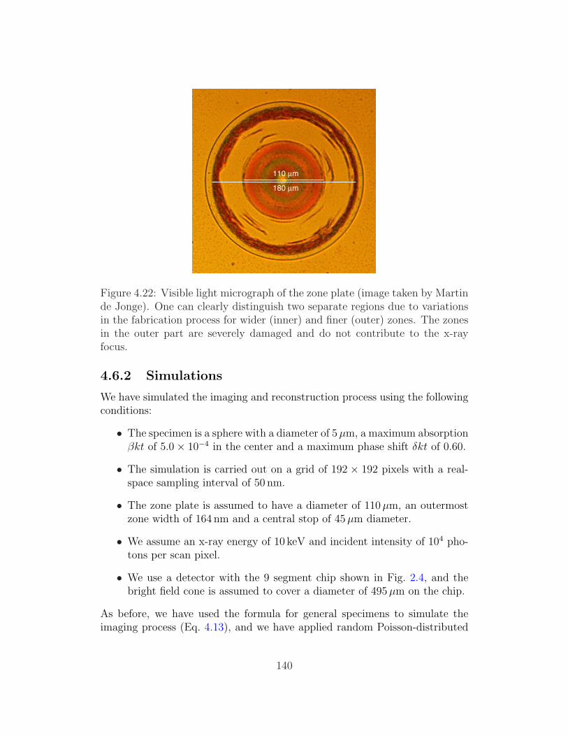
110 µm
180 µm
Figure 4.22: Visible light micrograph of the zone plate (image taken by Martinde Jonge). One can clearly distinguish two separate regions due to variationsin the fabrication process for wider (inner) and finer (outer) zones. The zonesin the outer part are severely damaged and do not contribute to the x-rayfocus.
4.6.2 Simulations
We have simulated the imaging and reconstruction process using the followingconditions:
• The specimen is a sphere with a diameter of 5 µm, a maximum absorptionβkt of 5.0× 10⁻⁴ in the center and a maximum phase shift δkt of 0.60.
• The simulation is carried out on a grid of 192 × 192 pixels with a real-space sampling interval of 50 nm.
• The zone plate is assumed to have a diameter of 110 µm, an outermostzone width of 164 nm and a central stop of 45 µm diameter.
• We assume an x-ray energy of 10 keV and incident intensity of 104 pho-tons per scan pixel.
• We use a detector with the 9 segment chip shown in Fig. 2.4, and thebright field cone is assumed to cover a diameter of 495 µm on the chip.
As before, we have used the formula for general specimens to simulate theimaging process (Eq. 4.13), and we have applied random Poisson-distributed
140
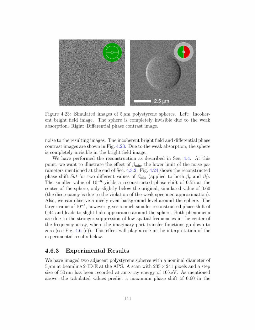
2.5 µm
Figure 4.23: Simulated images of 5 µm polystyrene spheres. Left: Incoher-ent bright field image. The sphere is completely invisible due to the weakabsorption. Right: Differential phase contrast image.
noise to the resulting images. The incoherent bright field and differential phasecontrast images are shown in Fig. 4.23. Due to the weak absorption, the sphereis completely invisible in the bright field image.
We have performed the reconstruction as described in Sec. 4.4. At thispoint, we want to illustrate the effect of βmin, the lower limit of the noise pa-rameters mentioned at the end of Sec. 4.3.2. Fig. 4.24 shows the reconstructedphase shift δkt for two different values of βmin (applied to both βr and βi).The smaller value of 10−6 yields a reconstructed phase shift of 0.55 at thecenter of the sphere, only slightly below the original, simulated value of 0.60(the discrepancy is due to the violation of the weak specimen approximation).Also, we can observe a nicely even background level around the sphere. Thelarger value of 10−4, however, gives a much smaller reconstructed phase shift of0.44 and leads to slight halo appearance around the sphere. Both phenomenaare due to the stronger suppression of low spatial frequencies in the center ofthe frequency array, where the imaginary part transfer functions go down tozero (see Fig. 4.6 (e)). This effect will play a role in the interpretation of theexperimental results below.
4.6.3 Experimental Results
We have imaged two adjacent polystyrene spheres with a nominal diameter of5 µm at beamline 2-ID-E at the APS. A scan with 235× 241 pixels and a stepsize of 50 nm has been recorded at an x-ray energy of 10 keV. As mentionedabove, the tabulated values predict a maximum phase shift of 0.60 in the
141

2.5 µm βmin = 10-6
Value at
center = 0.55
βmin = 10-4
Value at
center = 0.44
halo appearance
Figure 4.24: Phase reconstruction of a simulated sphere. The images showthe reconstructed δkt with βmin = 10−6 (left) and βmin = 10−4 (right). SeeSec. 4.3.2 for a discussion of βmin. At the bottom, we show a line profile throughthe center of the sphere. The higher βmin leads to a smaller reconstructed phaseshift and a slight halo appearance around the sphere, due to the suppressionof low spatial frequencies.
center of the spheres. The incident intensity was about 3.3 × 10⁵ photonsper scan pixel. Fig. 4.25 shows the incoherent bright field and differentialphase contrast images of the spheres. As expected, the spheres are completelyinvisible in absorption contrast. The reconstruction was done as describedbefore, with βmin = 10−6. Fig. 4.26 shows the radial power spectrum densitiesused to determine the noise parameters.
The resulting phase advance δkt is shown in Fig. 4.27. The bright featureson both spheres, which were also visible in the differential phase contrastimage, are unlikely to be part of the spheres, but rather dried remnants of thesolution in which the spheres are provided.
The reconstructed phase shift in the center of the spheres is on the orderof 0.42 radians. This is considerably lower than the expected value of 0.6radians listed above, or the result of the simulation, which was 0.55. Possibleexplanations are:
1. The slight halo appearance suggests a loss or incorrect weighting of lowspatial frequencies (see Sec. 4.6.2, where the low frequencies were delib-erately suppressed by increasing the lower cutoff of the noise parameter).Since the imaginary transfer is low at low frequencies, increased noisecan potentially suppress those frequencies. However, the signal is quitestrong in the DPC image, so that we do not expect noise to be thedominant parameter here.
142

2.5 µm 2.5 µm
Figure 4.25: Images of 5 µm polystyrene spheres obtained at 10 keV photonenergy. Left: Incoherent bright field image. The spheres are completely in-visible due to the low absorption. The red arrows point out top-up events asdescribed in Fig. 4.18. Right: Differential phase contrast image. Some struc-ture is visible on the spheres, which could be dried remnants of the solutionin which the spheres are provided.
More likely, again uneven illumination of the detector segments seemsto be the major reason (which leads to uncorrect weighting of frequencycomponents, rather than their suppression). The illumination presentat the time of the experiment is shown in Fig. 3.15 (the measurementsshown in Sec. 4.6.1 were done at a different time and characterize onlythe zone plate, not the illumination). We can notice a “blind spot” in theillumination, most likely due to a piece of dust on the monochromatorcrystal. This leads to one of the quadrant segments receiving about 25%less intensity than the others.
2. Another question which comes to mind is the accuracy of the tabulatedatomic scattering factors or polystyrene density, which determine theexpected phase shift. We have found one example of an independentphase shift measurement at a similar energy: In the famous descriptionof their first x-ray interferometer, Bonse and Hart report a measuredphase shift of 2π radians for 37.6 µm of lucite at a wavelength of 1.54 A(E = 8.05 keV) [89]. Using a density of 1.19 g/cm3 and a composition of(C5O2H8)n,8 the tabulated data of Henke et al. [9] result in an expectedphase shift of 2.01π radians, which is in excellent agreement with Bonseand Hart’s result. Therefore, we do not have a particular reason to ques-
8http://en.wikipedia.org/wiki/Acrylic_glass
143
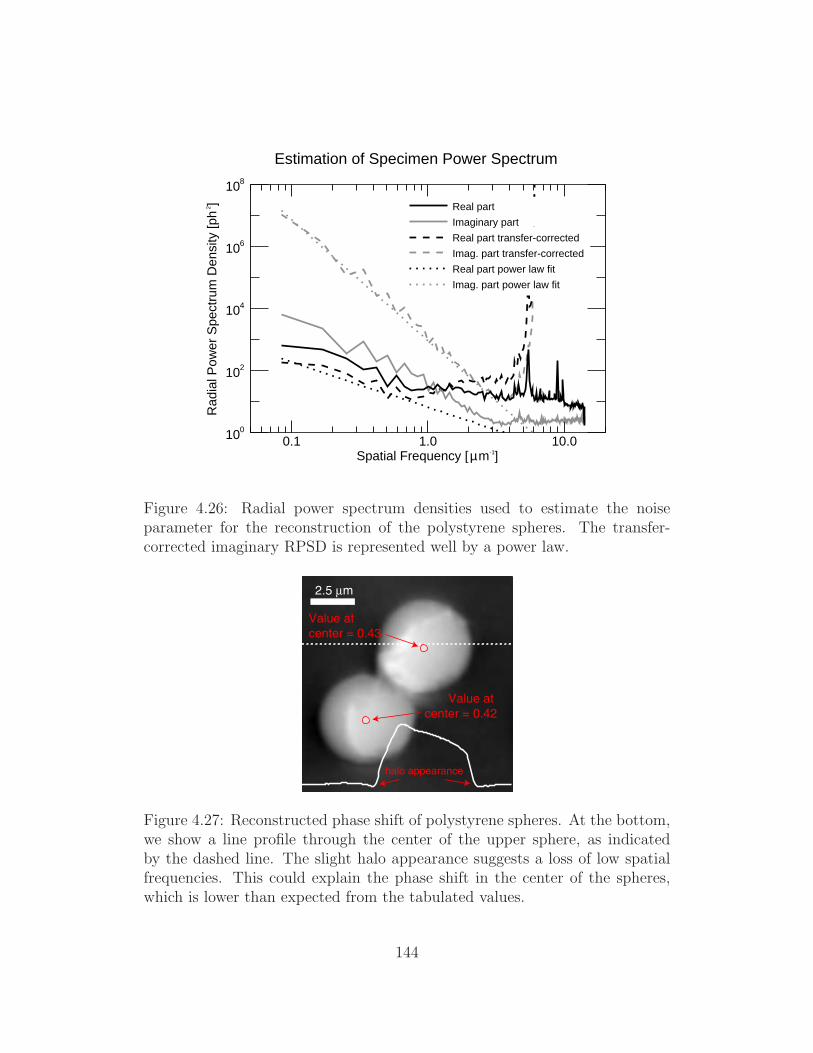
Rad
ial P
ower
Spe
ctru
m D
ensi
ty [p
h2 ]
108
106
104
102
100
Spatial Frequency [µm-1]10.01.00.1
Estimation of Specimen Power Spectrum
Imag. part power law fit
Real part power law fit
Imag. part transfer-corrected
Real part transfer-corrected
Imaginary part
Real part
Figure 4.26: Radial power spectrum densities used to estimate the noiseparameter for the reconstruction of the polystyrene spheres. The transfer-corrected imaginary RPSD is represented well by a power law.
2.5 µm
Value at
center = 0.43
Value at
center = 0.42
halo appearance
Figure 4.27: Reconstructed phase shift of polystyrene spheres. At the bottom,we show a line profile through the center of the upper sphere, as indicatedby the dashed line. The slight halo appearance suggests a loss of low spatialfrequencies. This could explain the phase shift in the center of the spheres,which is lower than expected from the tabulated values.
144
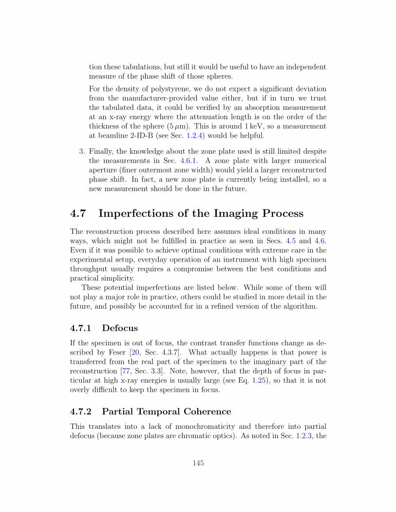
tion these tabulations, but still it would be useful to have an independentmeasure of the phase shift of those spheres.
For the density of polystyrene, we do not expect a significant deviationfrom the manufacturer-provided value either, but if in turn we trustthe tabulated data, it could be verified by an absorption measurementat an x-ray energy where the attenuation length is on the order of thethickness of the sphere (5 µm). This is around 1 keV, so a measurementat beamline 2-ID-B (see Sec. 1.2.4) would be helpful.
3. Finally, the knowledge about the zone plate used is still limited despitethe measurements in Sec. 4.6.1. A zone plate with larger numericalaperture (finer outermost zone width) would yield a larger reconstructedphase shift. In fact, a new zone plate is currently being installed, so anew measurement should be done in the future.
4.7 Imperfections of the Imaging Process
The reconstruction process described here assumes ideal conditions in manyways, which might not be fulfilled in practice as seen in Secs. 4.5 and 4.6.Even if it was possible to achieve optimal conditions with extreme care in theexperimental setup, everyday operation of an instrument with high specimenthroughput usually requires a compromise between the best conditions andpractical simplicity.
These potential imperfections are listed below. While some of them willnot play a major role in practice, others could be studied in more detail in thefuture, and possibly be accounted for in a refined version of the algorithm.
4.7.1 Defocus
If the specimen is out of focus, the contrast transfer functions change as de-scribed by Feser [20, Sec. 4.3.7]. What actually happens is that power istransferred from the real part of the specimen to the imaginary part of thereconstruction [77, Sec. 3.3]. Note, however, that the depth of focus in par-ticular at high x-ray energies is usually large (see Eq. 1.25), so that it is notoverly difficult to keep the specimen in focus.
4.7.2 Partial Temporal Coherence
This translates into a lack of monochromaticity and therefore into partialdefocus (because zone plates are chromatic optics). As noted in Sec. 1.2.3, the
145

monochromaticity E/∆E must be higher than the number of zones to avoidchromatic blurring. This condition is usually fulfilled in our case (typically,E/∆E = 103 . . . 104 for a grating or crystal monochromator), so that we donot expect a problem here.
4.7.3 Partial Spatial Coherence
Illumination of the zone plate with an extended (partially incoherent) sourcerather than a point (coherent) source leads to a widening of the focal spotand a loss of spatial resolution. As explained in Sec. 1.2.3, the point spreadfunction is then given by the convolution of the diffraction-limited spot andthe geometrical image of the source.
In practice, this can be overcome by closing down the slits which definethe source of the zone plate illumination. However, a loss of spatial resolutionis often accepted in return for higher flux and therefore shorter dwell times orhigher signal. Landauer [79, Sec. 5.8.1] shows that the extended source carriesall the way through to the final reconstruction, and can possibly deconvolvedfrom there if its intensity distribution is known well. Clearly, this cannotrecover the lost spatial resolution; it can only correct the magnitude of thereconstructed amplitude and phase.
4.7.4 Transverse Detector Misalignment
Transverse detector misalignment leads to an uneven intensity level on thedetector segments. For the most part, this can be avoided in practice witha motorized, scannable detector stage which allows for easy alignment (if theillumination itself is nicely symmetrical). Still, it would be instructive to studythe effects of misalignment on the reconstruction process. This is even moreimportant in the case of some microscopes / microprobes which scan the opticrather than the specimen for high resolution image acquisition, since in thiscase the detector would be “misaligned” from scan pixel to scan pixel. Asoftware correction between pixels might be required in such a case.
4.7.5 Uneven Pupil Illumination or Transmittance
This can easily happen in practice, either due to faults in the zone plate, or dueto unevenness in the illumination (for instance, the x-ray beam might be toosmall to fill a large zone plate uniformly). Consequently, the detector segmentswill be illuminated unevenly as was the case in Secs. 4.5 and 4.6. Even if theillumination is radially symmetric, an intensity shift in- or outwards strongly
146

affects the transfer functions if the detector is split in the radial direction (seeSec. 4.2.5). Therefore, this effect is definitely worth investigating more deeply.
First, it would be important to obtain a good measure of the actual inten-sity distribution. A pixelated detector such as a CCD would make this easy(the slow CCD readout is not an issue here, because only a single snapshot isrequired), but is currently not available in the instruments used in this thesis(see Sec. 1.2.4). Another option is an intensity map obtained by scanninga pinhole through the beam. We demonstrated this in Secs. 4.5 and 4.6 tomeasure the beam dimensions and for a qualitative evaluation of the illumina-tion, but we did not make full quantitative use of the data. In both of thesecases, an accurate registration between the intensity map and the segmenteddetector would be required.
Even without a finely resolved intensity distribution measurement, the rel-ative intensity of detector segments (in a specimen-free background region)contains useful information which could be taken into account in the recon-struction process. A first idea is to scale the images from the individual seg-ments such that their intensity level in the background region (relative to eachother) is set to the value expected from the pupil / segment overlap (givenby Ck(0, 0,f); see Eq. 4.20). However, this will not work because it assumesa wrong pupil / detector alignment to start with. Instead, we should havea good guess about the actual intensity distribution (independent of the de-tector) and adjust its position and extent for a best (least-squares) fit to themeasured intensity levels on the segments.
Another point to keep in mind is that the simplified version of the recon-struction filters (Eq. 4.29) requires a real, centrosymmetric pupil and a sym-metric detector configuration. If we want to account for an uneven intensitydistribution, we should use the general solution given by Eq. D.69.
4.7.6 Strong Specimen
If the weak specimen approximation (see Sec. 4.1.7) is not fulfilled, the processof image formation can no longer be simply described by linear transfer func-tions. Consequently, the reconstruction algorithm (which is based upon thetransfer function description) suffers. We have seen in our simulations thateven if the weak specimen approximation is violated, the specimen is usuallyreconstructed with its correct shape; the only effect was a general loss of themagnitude of the phase shift. It remains to be seen if a more detailed studyof the weak specimen approximation can reveal more information to improvethe reconstruction of strong specimens.
147

4.7.7 Noise
The reconstruction procedure accounts for random “white” noise (which hasa flat power spectrum) and filters it out in the final reconstruction. Note,however, that no analysis method can recover information that is lost due tonoise, so a sufficient signal to noise ratio is required (for instance, by usingsufficiently long dwell times).
Periodic noise will actually transfer to the final reconstruction. In partic-ular, the soft x-ray version of the detector is more prone to noise (like 60 Hzpickup from the power lines) due to the high sensitivity. Also, the x-ray beammight show periodic noise. If such noise cannot be suppressed before data ac-quisition, it can usually be treated by standard methods of image processing,like filtering in the spatial or Fourier domain (see Gonzalez and Woods [87] orother books on signal processing).
4.8 Conclusions and Future Work
We have studied the imaging process in a scanning transmission x-ray mi-croscope with a segmented detector, and we have adapted a Fourier filteringalgorithm to obtain a best estimate of the complex specimen function (whichincludes amplitude attenuation and phase shift). The potential for a quanti-tative reconstruction of the specimen phase shift is particularly attractive athigher x-ray energies, where the method could serve to determine the specimenthickness if its composition can be estimated well.
In the soft x-ray range, experiments with a germanium test pattern werein very good agreement with simulations and only moderately lower than ex-pected from tabulated values. This deviation could be explained with theviolation of the weak specimen approximation.
In the medium energy range, experiments with polystyrene spheres yieldeda phase shift about 15% lower than expected from the simulation (which wasbased on tabulated values of the atomic scattering factors). We believe thatthis is due to uneven illumination of the detector segments (leading to a loss orincorrect weighting of low spatial frequencies), which could not be quantifiedaccurately for the available measurement.
In the hard x-ray range, the reconstruction of polystyrene spheres yieldeda phase shift about 25% lower than the simulation (which was again basedon tabulated values). At this point, the reason for the discrepancy is unclear;uneven illumination and / or zone plate imperfections are the most likely ex-planation. Let us also point out that we do not have an independent measureof the actual specimen phase shift beyond the tabulated values of atomic scat-
148

tering factors.The following investigations are recommended for the future for a better
evaluation of the reconstruction method:
1. The expected phase shift, based on tabulated values, should be verified.It would be useful to get an independent measurement of the phase shiftof the same polystyrene spheres which were used in the experiments.
It should be noted that reliable tabulated values (along with knowl-edge about the composition of the specimen) are absolutely required ifquantitative phase contrast is to be used to determine specimen thick-ness. This is one of the main attractions of the method, because incombination with fluorescence measurements, it can give trace elementconcentrations rather than absolute amounts as explained in Sec. 1.4.1.
2. The experiments of Secs. 4.5 and 4.6 should be repeated with an evenmore thorough examination and optimization of the illumination pa-rameters. Fortunately, a new zone plate is currently being installed atbeamline 2-ID-E at the APS, which should operate close to its nominalperformance. Also, the medium energy experiments of Sec. 4.5 shouldbetter be done with a 9 segment chip, whose geometry is less sensitiveto radial intensity shifts.
3. The issue of noise and its influence in the suppression of low spatialfrequencies should be examined in more detail. In particular, a goodmeasure of the actual signal to noise ratio of image features would beuseful, because in practice we will rarely achieve a signal to noise ratioat the limit of photon statistics.
4. For the experiments recommended in item 2 of this list, the imperfec-tions described in Sec. 4.7 should be reduced as much as possible in theexperimental setup for a thorough investigation of the subject. If themethod is to be used routinely in the future, some of these imperfec-tions can probably be accepted if they are characterized well and can betaken into account in the reconstruction scheme. This concerns in par-ticular partial spatial coherence and uneven zone plate illumination /transmittance, both of which will often be present in regular microscopeoperation.
5. Finally, a more detailed comparison between this reconstruction methodand other methods for the integration of orthogonal gradient data (asmentioned in Sec. 3.4.5) would be desirable.
149

Chapter 5
Software Development
150

A considerable part of this thesis work was spent on developing software forinstrument control, data inspection, data storage, and data analysis. All soft-ware described here has been written in the Interactive Data Language (IDL),1
which is very suitable for quick image processing and data analysis due tothe availability of a command line interface, array-based calculations and anextensive library of mathematical and graphical-display routines. Since themicroscopes and microprobes used in this thesis work are routinely used byscientists from very different fields and not necessarily experts in x-ray micros-copy or any other field of instrumentation, and since the data analysis methodspresented here are of potential interest to them as well, care has been taken toprovide user-friendly and intuitive software along with good documentation.
5.1 Data File Implementations
For many tasks, in particular quantitative phase contrast analysis of the seg-mented detector data (see Chap. 4), various pieces of information are required,like
• the actual image data in different “calibrations” (see Sec. 5.2.1), and
• various additional parameters about
– the scan (pixel size, field size, scan direction, dwell time, the scandevices, photon energy, . . . );
– the microscope / microprobe setup (zone plate parameters, . . . );
– the specimen (type of sample, preparation parameters, . . . );
– the detector (geometry, calibration parameters, . . . ).
For productive work, it is very helpful to have most of that automated, i. e.have as much information as possible stored in the data file automatically.Otherwise, the operator has to remember to write everything down in thelogbook, and during data analysis it has to be entered manually from there.It has also happened that certain parameters were forgotten to be writtendown, which rendered the data useless in the end. Therefore, a set of data fileformats has been developed.
1http://ittvis.com/idl
151

5.1.1 The STXM 5 .sm File Format
The Stony Brook / NSLS STXM (see Sec. 1.2.4) has recently been upgradedto version 5 [21]. Part of this thesis work was to develop the data file im-plementation and the graphical instrument control program / file viewer (forthe latter, see Sec. 5.2). The file format (file extension .sm) was based onthe one of STXM version 4, but has been adapted to the new instrumentfeatures. While in STXM 4 the silicon detector calibration parameters werestored in a separate file, they have been included in the actual data file formatfor STXM 5, so that one file contains all the important information.
As a basis, the netCDF format2 was used. netCDF is one of the commonlyavailable scientific data formats (HDF is another example), an interface towhich is implemented in all major programming languages. The developersof scientific data formats pay particular attention to a platform independentimplementation (e. g., independent of processor byte ordering and word width),and to allowing the storage of various attributes (which describe the data)along with the data itself. Therefore, scientists using our microscopes can, ifthey want, write their own analysis software in the language of their choicewith moderate effort.
It should be noted that our data files only store the raw data, as recordedby the instrument. If the user wants the calibrated data, it is calculated whenthe file is read, using the calibration parameters stored as attributes. TheSTXM 5 data format has been documented in detail.3
5.1.2 The Segmented Detector .sdt File Format
At the APS beamlines where we are installing the segmented silicon detector,currently not all of the information mentioned above are stored in the data files(for example, the zone plate parameters and detector calibration parametersare missing). While there is an effort underway to implement the necessarychanges, for the time being we have developed a special intermediate datafile format to hold the segmented silicon detector data. The idea is that thenative APS data files are converted to the .sdt format soon after acquisition,while all the information is freshly available. In this process, all the requiredparameters are added to the intermediate format. Then, at a later point, onecan read the intermediate format and has all the parameters available withouthaving to query the logbook.
2http://www.unidata.ucar.edu/software/netcdf/3see the STXM 5 User Manual at http://xray1.physics.sunysb.edu/user/manuals.
php
152

The .sdt file format is based on the STXM 5 .sm format. Using theSTXM 5 format directly as intermediate format for APS data was not practicaldue to the differences in hardware. Again, we store only the raw data andcalibrate when reading. Most of the parameters stored are the same, andagain we use the netCDF format as a basis.
5.2 A Graphical User Interface for Microscope
Control and Data Inspection
A Graphical User Interface program (sm gui) has been developed to controland view the data of STXM 5. For a screenshot, see Fig. 5.1. As the instru-ment is used in large part by non-experts in x-ray microscopy, it is importantto provide an intuitive tool with a graphical interface (rather than crypticcommand-line programs) and extensive documentation.3 The program canrun in two different modes:
• The full-featured microscope control mode which is used to operate themicroscope hardware. A client-server system has been developed4 so thatthe low-level instrument control software runs on a dedicated computernext to the microscope, while the user interface (graphical or command-line) can run on a separate computer (like the operator’s personal laptop)which communicates with the former over the network, possibly from off-site.
• A reduced “display-only” mode which has all microscope control featuresstripped off, but can run on any computer (independent of microscopehardware) to view previously recorded data files. To allow all users toview their data on their own computers, we provide a precompiled versionof the program to run under the freely available IDL Virtual Machine.
Some features of the program are as follows.
• In microscope control mode, one can
– set up and start scans;
– move motors and devices in the microscope;
– change the monochromator energy;
– calibrate the segmented silicon detector;
– insert and remove detectors; and
4implemented by Holger Fleckenstein
153

Figure 5.1: Screenshot of sm gui, the STXM 5 microscope control program.
154

– record and recall alignment positions.
• One can view and inspect data, and easily switch between different signaltypes and detector segment combinations (see Sec. 5.2.1).
• The program provides quick access to all parameters of interest eitherdirectly in the main window, or with a few mouse clicks or keystrokes.
• Intensity scaling (brightness and contrast adjustment) is available, alongwith a histogram of the data.
• Data can be exported to standard image file formats (for example PNG,JPG, or EPS).
• One can print a scan summary (image and some important scan param-eters), for example to be pasted into a logbook.
• One can display image statistics, do some basic image processing (smooth-ing, filtering), display the power spectrum, and so on.
• The scan data can be exported directly into a variable on the IDL com-mand line, where one has all the features of the programming languageavailable for sophisticated data analysis.
Although sm gui was written in particular for microscope operation anddata inspection of STXM 5, it is generally optimized to view segmented detec-tor data from any scanning microscope or microprobe. Therefore, it has beenenabled to read and display data from the APS (recorded with the segmentedsilicon detector) as well, which is very useful for the analysis of differentialphase contrast data.
5.2.1 Signal Types for Segmented Detector Data
As described in Sec. 2.5.4, scanning microscopes can record a number of dif-ferent signals (“detectors”) for each scan pixel. In particular, if we use asegmented detector, the signal of each segment is recorded and stored sep-arately. Additionally, a clock signal is often recorded as a measure of theactual dwell time per pixel, and possibly several other signals. Consequently,a two-dimensional scan in a scanning microscope results in a three-dimensionaldataset. In sm gui, we offer the option to view any arbitrary “slice” out ofthat dataset (e. g., the image consisting of the signal from detector segment 3).Moreover, we offer to view that data in different signal types, or “calibrations”.The three basic types are:
155

• The raw data as it is recorded by the instrument. For signals recordedby an analog to digital converter (ADC), this is the integer numbercorresponding to the voltage measured, depending on the number of bitsand the range of the ADC. For any counted signal (including the voltageswhich have been converted to a pulse stream by a voltage to frequencyconverter, or V2F), this is the integer number representing the counts.This signal type is most readily available, but is mostly interesting forinstrument debugging.
• If the original data was a voltage, we can convert the raw data back tothe voltage by applying the calibration data of the ADC or V2F.
• In the case of the segmented silicon detector, we can convert the voltageto a photon count rate by applying the detector calibration formula (seeSec. 2.6). This is usually the data of interest, but of course it is onlyreliable if the detector has been calibrated properly and the calibrationparameters are available. Sometimes, the raw data is good enough asa qualitative signal (because it is roughly proportional to the photoncount).
Each of the signals (detector segments) can be viewed in any of these signaltypes. But the actual “beauty” of the segmented detector is to combine seg-ments in different ways, for example to add them up to obtain an incoherentbright field image, or subtract opposite segments for a differential phase con-trast image. Therefore, a fourth signal type is provided where a number ofpredefined linear combinations of detector segments can be displayed.
Recently, a fifth mode has been added, where any arbitrary combination(not necessarily linear) of detector signals can be calculated under user control(without editing the program source code) for full flexibility. For more detailsabout signal types, see the STXM 5 User’s Manual mentioned above.
5.3 Phase Reconstruction Software
A set of routines has been developed to implement the quantitative amplitudeand phase reconstruction algorithm described in Chap. 4. As input data files,one can use the NSLS STXM 5 files, the segmented detector file format de-scribed above, or the raw APS data files (in which case one has to providezone plate and other parameters separately).
These routines have been implemented as methods of a “phase reconstruc-tion” object class. An object-oriented approach, compared to the classical
156

procedural approach, allows for a cleaner modular implementation of the sep-arate steps of the reconstruction process, because the object keeps the data, allthe parameters and the associated calculations together. This makes it easier,for instance, to study the effect of varying one reconstruction parameter (e. g.,the noise level, power spectrum fit parameters, or background region) whilekeeping the others constant. Moreover, an object implementation is a goodbasis for a graphical user interface to the reconstruction process (to be writtenin the future).
A separate file format has been developed to store the result of the re-construction process. Rather than the resulting complex specimen function,only the original data along with all analysis parameters are stored, so that areconstruction can be reproduced unambiguously, or specific parameters canbe varied at a later time. Again, the netCDF format has been chosen for thereconstruction data files.
157

Chapter 6
Summary and Outlook
158

Phase Contrast in Scanning X-ray Microscopy
Scanning x-ray microscopes and microprobes are unique tools for the nanoscaleinvestigation and characterization of specimens from the life, environmental,materials and other fields of sciences. In comparison to electron microscopy,x-rays do not provide quite as high resolution, but have other advantages suchas larger penetration distance for the investigation of thick specimens in theirnatural environment.
Phase contrast is a valuable technique which complements the more estab-lished methods of absorption imaging and fluorescence spectroscopy. In thesoft and intermediate x-ray range, absorption imaging is often carried out alongwith with XANES (X-ray Absorption Near-Edge Structure) investigations forcombined spectro-microscopy. Here, phase measurements can provide strongcontrast with reduced radiation dose compared to absorption, when imagesare recorded below an absorption edge.
In the medium and hard x-ray range, a strong focus lies on the use of x-rayfluorescence to map and quantify trace elements, whose catalytic propertiesplay an important role in the functioning of cells. However, absorption isvery weak at the energies required to stimulate fluorescence emission from theelements of interest. Furthermore, the fluorescence yield of low-Z elements(which make up the bulk of biological tissue) is very low, so that fluorescenceor absorption cannot image the specimen ultrastructure, or tissue, well. Thisis a problem not only for the characterization of specimens and interpretationof fluorescence data, but even for a seemingly simple task such as locatingindividual cells when a new sample is inserted into the instrument. Here,phase contrast can fill the gap and provide quick high-contrast overview scansas well as detailed images of ultrastructure, which can help to put trace elementinto their cellular context.
A Segmented Detector for Phase Contrast Measurements in a Scan-ning Microscope
A segmented detector can be used to provide absorption and phase contrastsimultaneously in a scanning instrument. In fact, a detector with a smallnumber of segments can very efficiently extract phase information from thespecimen, while offering fast readout and smaller, more manageable amountsof data compared to a fully pixelated detector such as a CCD.
Such a segmented detector had been previously developed for soft x-rayapplications. In Chap. 2 we have described the adaptation of that detector(again in collaboration with the Instrumentation Division at Brookhaven Na-tional Laboratory) and its characterization for use at higher x-ray energies. It
159

can be installed in parallel with the standard energy-dispersive detector forcombined fluorescence and phase contrast imaging. The detector consists ofa segmented silicon photodiode chip and charge integrating electronics. Thechip, produced by the Max Planck Semiconductor Laboratory, is available inseveral segmentations. It has very low leakage current (important in particularfor low flux, low photon energy applications) and provides excellent quantumefficiency up to about 10 keV photon energy. It can still be used at higherenergies (up to about 20 keV), but the thickness limits the quantum efficiencydue to the increased absorption length in silicon. The chip suffers from radi-ation damage if the segmented p-side is exposed to radiation. At low photonenergies, this can be completely avoided by illumination from the n-side. Athigher energies, where a considerable fraction of the radiation passes throughthe chip, radiation damage is noticeable, but can be tolerated if the detectoris calibrated regularly and the chip is repaired by annealing every few months.
The integrating electronics consists of 10 channels for readout of up to 10segments. It has low noise, and the dynamic range can be adjusted over awide range of signal levels (determined by the photon energy, the photon fluxand the integration time). Each channel collects the charge produced in agiven segment during the integration time. For fast overview scans and highresolution images in fly scan mode, the integration time is matched to the pixeldwell time. For slow step scans, usually used for fluorescence measurementsand alignment, the detector integration and pixel dwell times can be decoupledfor increased dynamic range. The detector system can be absolutely calibratedin terms of x-ray flux.
We have installed the detector at beamline 2-ID-E at the Advanced PhotonSource (APS), where it has been in routine use for more than a year andshows excellent performance in day-to-day use. The installation at additionalmicroscopes at the APS and elsewhere is currently underway or planned forthe near future.
Differential Phase Contrast
Differential phase contrast (DPC) provides a measure of the specimen phasegradient. It is easily available from a segmented detector by simple differenceimages of opposing segments, even in real-time while the data is being acquired.
In Chap. 3, we have presented calculations and several examples show-ing that at higher photon energies, DPC provides vastly superior image con-trast compared to absorption. In particular around 10 keV (an energy whichprovides access to a wide range of transition metals in x-ray fluorescence),many specimens are just invisible in absorption at moderate exposure times,whereas phase contrast is quite strong. In fact, at beamline 2-ID-E, the seg-
160
mented detector has proven invaluable for quick specimen localization as wellas high resolution transmission images of specimen ultrastructure. We havealso demonstrated phase contrast in conjunction with fluorescence trace ele-ment maps by the example of a phytoplankton cell.
For quantitative analysis, DPC is less useful due to the differential natureand directional dependence of the signal. However, it would be extremelybeneficial to determine the absolute phase shift of the specimen, to obtaininformation about the thickness or mass of the specimen. This can be used tocalculate elemental concentrations, which are the actual drivers of biologicalprocesses (rather than absolute amounts).
It is straightforward to integrate phase gradient data, but the resultingimages suffer from the simultaneous integration of noise and other artifacts.Furthermore, a simple integration does not account for the limited spatialfrequency transfer of the optical system. While more sophisticated methodsfor the integration of orthogonal gradient data might prove useful in the future,we have focused on the technique described in the next paragraph to determinephase shifts quantitatively.
Quantitative Phase Reconstruction by Fourier Filtering
In Chap. 4, we have first reviewed the process of image formation in a scan-ning microscope with a segmented detector. We have calculated the contrasttransfer functions of such an imaging system, and we have evaluated the phasecontrast performance of different detector geometries considering theoreticaland practical aspects.
We have then described the adaptation of a Fourier filtering algorithmwhich had been developed in the field of scanning transmission electron mi-croscopy. We have advanced the technique for the optimal, quantitative re-construction of specimen amplitude and phase shift in the presence of noise.Simulations in the soft, medium and hard x-ray range with simple test speci-mens gave very good results, which demonstrates the potential of the algorithmfor practical applications.
Soft x-ray experiments were in very good agreement with the simulations.Medium and high energy experiments suffered somewhat from imperfect ex-perimental conditions, but still gave reasonable results. We have found thatgood knowledge about the exact illumination conditions is crucial for a goodquantitative reconstruction. Furthermore, the lack of an independent measureof the specimen phase shift beyond the tabulated values of atomic scatteringfactors made it difficult to evaluate the phase reconstruction in more detail.
161
Software Development
In Chap. 5, we have reported on the development of software covering allaspects of this thesis work. It has proven useful for a streamlined procedureof data inspection and analysis, and it will make it easy to perform furthersimulations of phase reconstructions under different conditions.
As phase contrast is expected to become routinely available in several mi-croscopes and microprobes, it is important to provide user-friendly softwarefor the standard user who is not an expert in instrumentation and x-ray mi-croscopy. We have provided a graphical user interface for instrument controland data inspection, and we have built a strong basis for a similar interface tothe amplitude and phase reconstruction procedure described above.
Future Work
We have achieved a lot, but the story doesn’t end here. First, the segmenteddetector is to be installed at a number of instruments at the Advanced PhotonSource as well as the Australian synchrotron. This will significantly increasethe number of potential applications. However, for routine use the imple-mentation of the detector in the existing data acquisition systems has to beoptimized by storing the relevant detector parameters (like calibration param-eters) in the data files.
For a more detailed evaluation of the quantitative phase reconstructionprocess, further experiments with optimized illumination conditions shouldbe performed. Also, independent measurements of the specimen’s phase shiftwould be useful to verify the results. Then it should be investigated to whichdegree the stringent conditions can be relaxed without degrading the perfor-mance of the technique too much, because every-day operation usually requiresa tradeoff between optimal performance and practical simplicity. We shouldbe able to account for the most relevant imperfections in a refined version ofthe reconstruction algorithm.
The next step will be to use the technique beyond test specimens, in realpractical applications (in collaboration with scientists from those fields) todetermine specimen mass and therefore trace element concentrations. To buildtrust in the method, an independent verification would be useful, for exampleby measuring a number of individual cells and comparing with average valuesobtained from bulk measurements. Let us emphasize again that for the purposeof determining specimen thickness or mass from the total phase shift, goodknowledge about the specimen’s composition and refractive index is essential.
Looking further into the future, we can imagine significant hardware im-provements as well. As the demand from other applications grows, we expect
162
that pixel detectors with fast readout will become available. They might makeit unnecessary to develop dedicated segmented detectors for scanning micro-scopes, whose use is limited beyond this particular type of instrument. Thedata from pixel detectors can easily be rebinned for the equivalent of a seg-mented detector (where the segmentation can be chosen arbitrarily at the timeof rebinning), but the wealth of information contained in the full microdiffrac-tion pattern at each scan pixel will also open the door for different analysistechniques.
A technique which we did not touch on much is the use of the dark fieldor small angle scattering signal (see Sec. 1.3.5). This signal is available inprinciple from a configured detector with dedicated segments covering the areaoutside the bright field cone. However, since the scattering signal is orders ofmagnitude weaker than the direct beam, those segments should be read out bydedicated electronics channels with much higher sensitivity for a good qualitysignal. The development of detector electronics with such different channels,or greatly increased dynamic range, might be worthwhile.
Another area with potential for progress would be the development of ger-manium chips, which could be used for direct x-ray detection at higher energiescompared to silicon.
163

Appendix A
Terms and Acronyms
164

ADC Analog to digital converterAPS Advanced Photon SourceBF Bright fieldCTF Contrast transfer functionCCD Charge coupled deviceDPC Differential phase contrastFT/FFT (Fast) Fourier transformGUI Graphical user interfaceMCA Multichannel analyzerMPI-HLL Max Plank Institute Halbleiterlabor (Semiconductor
Laboratory)NA Numerical apertureNSLS National Synchrotron Light SourceOSA Order-sorting aperturePC Phase contrastPSF Point spread functionRMS Root mean squareRPSD Radial power spectrum densityS/H Sample and hold circuitSNR Signal to noise ratioSFXM Scanning fluorescence x-ray microscope / microscopySTEM Scanning transmission electron microscope / microscopySTXM Scanning transmission x-ray microscope / microscopyTXM (Full-field) Transmission x-ray microscope / microscopyV2F Voltage to frequency converterZP Zone plate
Table A.1: List of terms and acronyms
Table A.1 lists some common terms, acronyms and abbreviations which areused throughout this document.
165

Appendix B
Fourier Transform Relations
166

This appendix summarizes some basic Fourier transform (FT) definitions andrelations which are used in Chap. 4 and Appendix D. For more details andproofs, the reader is referred to Brigham [90], Bracewell [91], or any otherstandard book on Fourier transforms.
In the following, all integrals are from −∞ to +∞ unless otherwise noted.We assume all functions to be two-dimensional, as is usually the case in imag-ing, although there is no fundamental difference between the one- and two-dimensional cases. We denote real space functions with lower-case letters, andtheir Fourier transforms with the corresponding upper-case letters, unless oth-erwise noted. The real space variable is r = (x, y), and the Fourier variable(spatial frequency) is f = (fx, fy).
B.1 Forward and Inverse Fourier Transform
We use the following definition for the forward Fourier transform of a functionf(r):
FT f(r) = F (f) =
∫dr f(r) exp(−2πi rf). (B.1)
The corresponding inverse FT is then given by
FT−1 F (f) = f(r) =
∫df F (f) exp(+2πi rf). (B.2)
Note that F (0) =∫
drf(r) is the integral of the function f over the wholex, y (image) plane.
B.2 Fourier Transform Properties and Sym-
metry
The basic properties of Fourier transforms are summarized in Table B.1. Sym-metry properties of complex functions are listed in Table B.2.
B.3 Convolution and Convolution Theorem
The convolution h(r) of two functions f(r) and g(r) with respect to the vari-able r is defined as
h(r) = f(r)⊗r g(r) =
∫dr′ f(r′) g(r − r′). (B.3)
167

Property Real space Fourier spaceLinearity a · f(r) + b · g(r) a · F (f) + b ·G(f)Symmetrya F (r) f(−f)Scaling f(a · r) 1/|a|F (f/a)Shift f(r − r0) exp(−2πir0f) F (f)Modulation exp(+2πirf 0) f(r) F (f − f 0)Derivative ∂f(r)/∂x 2πifx F (f)
aIn other words, a double forward FT reproduces the original function, reflected aboutthe origin.
Table B.1: Fourier transform properties (after Brigham [90, Table 3.2]).
Real space f(r) Fourier space F (f)Real Real part even, imaginary part oddImaginary Real part odd, imaginary part evenReal even, imaginary odd RealReal odd, imaginary even ImaginaryReal and even Real and evenReal and odd Imaginary and oddImaginary and even Imaginary and evenImaginary and odd Real and oddComplex and even Complex and evenComplex and odd Complex and odd
Table B.2: Fourier transform symmetries (after Brigham [90, Table 3.1]).
By exchanging variables, r′ → (r − r′), Eq. B.3 can be rewritten as
h(r) = f(r)⊗r g(r) =
∫dr′ f(r − r′) g(r′), (B.4)
which means that it does not matter which one of the functions is invertedand shifted.
The convolution theorem states that in Fourier space the convolution turnsinto a simple multiplication, or
H(f) = F (f) ·G(f). (B.5)
The convolution of two inverted functions can easily be calculated by substi-
168

tuting a = −r:
f(−r)⊗r g(−r) = f(a)⊗r g(a)
=
∫dr′ f(a− r′) g(r′)
=
∫dr′ f(−r − r′) g(r′). (B.6)
B.4 Correlation and Correlation Theorem
The correlation z(r) of two functions f(r) and g(r) with respect to the variabler is defined as
z(r) = f(r) ?r g(r) =
∫dr′ f(r′) g(r + r′). (B.7)
Note that the correlation is equivalent to the convolution if either of the twofunctions f or g is even. In the case of scanning x-ray microscopy, this isusually true for the pupil and therefore for the probe function. The correlationtheorem states that
Z(f) = F (f) ·G∗(f), (B.8)
where G∗ is the complex-conjugate of G.If f and g are the same function, z is usually called the autocorrelation
of f . For the case of different functions f and g, the term crosscorrelation isused.
B.5 Parseval’s Theorem and the Conservation
of Energy
Parseval’s theorem states that∫
dr |f(r)|2 =
∫df |F (f)|2 . (B.9)
If Fourier transforms are used to propagate wave fields, this can be interpretedas conservation of energy, intensity or photons.
169

B.6 The Dirac Delta-Function
The Dirac delta function,1 often referred to as impulse function, is an impor-tant concept in Fourier analysis. It provides a mathematical representation ofinfinitely small or short quantities with finite “strength,” like a point source.In this section, we want to adhere to general convention and denote it witha lower-case δ, although in Chap. 4 we use an upper-case ∆ to distinguish itfrom the real-part decrement of the refractive index. It is usually defined by
δ(r − r0) = 0 for r 6= r0, and∫dr δ(r − r0) = 1. (B.10)
This means the magnitude at r = r0 is undefined (a sloppy description isto say that it is infinity), but the integral is defined and finite. The mostimportant property is the sifting property:
∫dr δ(r − r0) f(r) = f(r0). (B.11)
If we substitute f(r) = exp(+2πirf) and r0 = 0 in this equation, we canrecognize the inverse Fourier transform of the delta function (see Eq. B.2), or
∫dr δ(r) exp(+2πirf) = exp(+2πi · 0 · f) = 1. (B.12)
The corresponding forward transform then states that
∫dr 1 · exp(−2πirf) =
∫dr exp(−2πirf) = δ(f). (B.13)
B.7 The Discrete Fourier Transform
Data analysis and numerical simulations are usually carried out on a grid ofdiscrete data points (two-dimensional in the case of imaging), which representsan approximation or sampled version of the “true” continuous quantity. Weuse the following definition of the discrete 2-D forward Fourier transform:
F (u, v) =1
NxNy
∑x,y
f(x, y) exp
[−2πi
(ux
Nx
+vy
Ny
)], (B.14)
1Strictly speaking, it is a distribution rather than a function, but we want to keep itsimple here.
170

where x, y and u, v are the indices of the data points in the real and Fourierspace arrays, respectively, and Nx, Ny are the numbers of data points in thetwo dimensions. The inverse transform is then given by
f(x, y) =∑u,v
F (u, v) exp
[+2πi
(ux
Nx
+vy
Ny
)]. (B.15)
Note that F (0, 0) =∑
x,y f(x, y)/(NxNy) is the mean value of the real spacearray, also often called the DC value or offset (which stands for direct currentand stems from the Fourier analysis of electrical signals).
If ∆x and ∆y are the real space sampling intervals, the Fourier spacesampling intervals are given by
∆u =1
Nx∆x, and (B.16)
∆v =1
Ny∆y. (B.17)
For an even number of pixels in any dimension i, it is convenient to arrangethe data points in the Fourier transform array such that the frequencies aregiven by
1
Ni∆i
(−Ni
2,−(Ni
2− 1), . . . ,−1, 0, 1, . . . , Ni
2− 1
)(B.18)
such that the zero frequency is at the pixel just right and above of the center(in the common convention of image processing, where zero is at the lowerleft of the image). For an odd number of pixels, one would use the followingarrangement:
1
Ni∆i
(−(Ni−12
), . . . ,−1, 0, 1, . . . , Ni−12
)(B.19)
such that the zero frequency is right in the center. The frequency 1/(2∆i) iscalled the Nyquist frequency.
The Fourier transform properties listed in Sec. B.2 all have an equivalentin the discrete case, as do the convolution (B.3) and correlation (B.4). Note,however, that the sampling procedure introduces some specific artifacts like aband limit and an implicit periodicity. For details, the reader is referred tothe literature [90, 91].
With the definition of the discrete Fourier transform above, Parseval’s the-orem (see Sec. B.5) takes the form
∑x,y
|f(x, y)|2 = NxNy
∑u,v
|F (u, v)|2 . (B.20)
171

An appropriate correction has to be made if Fourier transforms are used topropagate wave fields and the total intensity (number of photons) is to bepreserved.
Discrete Fourier transforms can be computed quickly using Fast FourierTransform (FFT) algorithms (see, e. g., Brigham [90]). Implementations ofsuch algorithms are readily available for all major programming languages.
172

Appendix C
The Wiener Filter
173

The Wiener filter, which was first described by Levinson [92], is commonlyused to remove artifacts of the measuring process from noisy data, and thequantitative amplitude and phase reconstruction method described in Chap. 4and Appendix D is a simple extension of it. In the following we want to givea brief outline roughly following Landauer [79]. Further information is given,for example, by Gonzalez and Woods [87], Press et al. [93] or other books onsignal processing.
Assume that a “true” function h(x) is to be measured, but in the measuringprocess it gets smeared out or corrupted (mathematically: convolved) with aknown instrument function t(x). Moreover, statistical noise described by afunction n(x) is added, so that the measured function is
s(x) = h(x)⊗ t(x) + n(x). (C.1)
Taking the Fourier transform and using the convolution theorem, we get
S(f) = H(f)× T (f) + N(f), (C.2)
where f is the Fourier variable and S(f), H(f), T (f) and N(f) are the Fouriertransforms of s(x), h(x), t(x) and n(x), respectively. t(x) is often called theimpulse response of the instrument, or the point spread function in an imagingsystem (the image of a point, or delta function, object). Its Fourier transformT (f) can be called the frequency transfer, or in incoherent imaging systems themodulation transfer function (MTF). Note that in imaging the exact nomen-clature also depends on whether the quantities describe amplitude or intensity.
If there was no noise, and if the frequency response T (f) did not have anyzeroes, we could obtain the true signal spectrum by a simple inverse filter:
H(f) =S(f)
T (f). (C.3)
However, in practical applications, the frequency transfer can be quite low atcertain (usually high) frequencies so that the noise dominates the signal, andthe inverse filter would just amplify that noise. The Wiener filter calculatesan estimate
H(f) = W (f)× S(f) (C.4)
such that the root mean square (rms) error
ε =
∫df
⟨∣∣∣H −H∣∣∣2⟩
(C.5)
is minimized. W (f) is called the Wiener filter function. The brackets 〈〉
174
indicate an expectation value which averages over many measurements of thenoisy data S. Since the integrand of Eq. C.5 is real and greater than orequal to zero for all f , we can perform the minimization for each value of findependently and omit the integral in the following. Substituting Eq. C.4into Eq. C.5 and minimizing with respect to W , we obtain
∂ε
∂W= 〈S∗ (WS −H)〉 = 0. (C.6)
Now we can subsitute Eq. C.2 into Eq. C.6, and if we assume that N and Hare uncorrelated, we get
W |H|2 |T |2 − |H|2 T ∗ + Wη = 0, where η =⟨|N |2⟩ . (C.7)
We solve for W and substitute the result into Eq. C.4 to obtain the bestestimate of H(f) as
H =T ∗
|T |2 + βS, where β =
η
|H|2 . (C.8)
An alternative, but equivalent way to write this is
H =|HT |2
|HT |2 + η
S
T. (C.9)
How can we interpret this? If we look at Eq. C.9, we see on the very rightthat first a simple inverse filter is applied to the measured data S. Then anadditional filter of the form
|HT |2|HT |2 + η
(C.10)
is applied, which is close to one at frequencies where the power spectrum ofthe transferred signal |HT |2 is large compared to the expectation value ofthe noise power spectrum η, and close to zero at frequencies where the noisedominates the transferred signal. In other words, the Wiener filter consists ofan inverse filter plus an additional filter which suppresses frequencies whichare dominated by noise.
To calculate the filter function W , we need to separately estimate the powerspectra of the transferred signal |HT |2 and the noise η. In many practical cases,this can easily be read from a plot of the power spectrum of the measured signal|S|2 (see Fig. C.1). Usually one can see the power spectrum of the signal whichdeclines down to a noise floor at higher frequencies. The noise level can thenbe extrapolated into the region dominated by the signal, and vice versa.
175

|HT|2 (deduced)
|N| 2 (extrapolated)
|S|2 (measured)
log
scal
e
f
Figure C.1: Estimation of the signal and noise power spectra for the calculationof the Wiener filter; see text. Figure modified from Press et al. [93].
For a graphical illustration of the Wiener filter, in Fig. C.2 we plot theModulation Transfer Function (MTF) of an apodized lens, as is often usedin x-ray microscopy (see Sec. 1.2.3), as an example for a frequency transferfunction T . Also shown are Wiener filter functions of the form
W =MTF∗
|MTF|2 + β(C.11)
(compare Eq. C.8), where we have used a constant β instead of the truefrequency-dependent ratio of noise to signal spectrum. We can see that at highfrequencies, where the value of the MTF is small, the inverse filter (β = 0)would boost the noise to infinity, making the result useless. As we increase β,those frequencies are suppressed more and more, until (when β becomes toolarge) the signal is overly suppressed. Often, instead of the more elaboratepower-spectrum estimation described above, one can just use this version ofthe Wiener filter and adjust β interactively to yield the “visually best” results[87].
The application of the Wiener filter to remove the effects of the zone platetransfer function in a scanning transmission x-ray microscope was demon-strated by Jacobsen et al. [94].
176

MT
F V
alue
1.0
0.8
0.6
0.4
0.2
0.0
Wie
ner
Filt
er V
alue
20
15
10
5
0
Normalized Spatial Frequency210-1-2
(inverse filter)
Wiener Filter W = MTF* / (MTF2 + β)
MTF
0.10.01
β = 0.001
β = 0
Figure C.2: Graphical illustration of the Wiener filter. The scale on the rightis for the MTF (dashed curve), whereas the scale on the left is for the Wienerfilter functions. Compared to the inverse filter, the Wiener filter suppressesfrequencies with low transfer, which are dominated by noise. The correct valueof the noise parameter β is crucial for good quantitative results.
177
Appendix D
Detailed Derivation of ImageFormation and SpecimenReconstruction
178
In this appendix, we want to give a more detailed derivation of the imageformation and Fourier filter reconstruction results of Chap. 4. We will usegeneral optics concepts from Goodman [14] and Born and Wolf [95], and thederivation of image formation in STXM partly follows Vogt et al. [32]. Forsegmented detector imaging and the Fourier filtering method, we follow Mc-Callum, Landauer and Rodenburg [76–79]. Also, Morrison’s results [29, 53]are used in the derivation of segmented detector imaging.
D.1 Image Formation in a Scanning Transmis-
sion X-ray Microscope
To propagate wave fields through the microscope, we will use the Fresnelintegral [14, 95] with the Fraunhofer approximation where noted. Note onceagain that some signs depend on the convention used for wave propagation; inour case we write a wave propagating in the +z direction as exp[−i(kz−ωt)].To propagate a wave field ψ from a plane of coordinates r to a plane r′ locateda distance z away, we write the Fresnel integral as
ψ′(r′) =exp(−ikz)
iλz
∫dr ψ(r) exp
(−ik
2z(r′ − r)2
)(D.1)
=exp(−ikz)
iλzexp
(−ik
2zr′ 2
)×
×∫
dr ψ(r) exp
(−ik
2zr2
)exp
(ik
zrr′
), (D.2)
where k = 2π/λ is the wave number and λ is the x-ray wavelength. Allintegrals go from −∞ to +∞ unless otherwise noted.
D.1.1 Wave Propagation to the Detector Plane
Figure D.1 again shows the optical setup of a scanning transmission x-raymicroscope as reference for the calculations below. In the first part of thisderivation, we want to specifically label the wave fields ψ and coordinates rwith subscripts according to the corresponding plane. These subscripts will bedropped later. A point (coherent) source, located at a plane with coordinatesr1 illuminates a Fresnel zone plate (ZP, see Sec. 1.2.3) with coordinates r2,located a distance d1 away. The zone plate acts like a thin lens and producesa focus in the specimen plane at coordinates r3, located a distance d2 fromthe zone plate. After being modulated by the specimen transmission function,
179

zone plate withpupil fn. P(f4) OSA
sampleh(r3)
probe p(r3 - r0)
coherentsource
scandisplacement(r
0)
DetectorwithresponsefunctionRk(f4)
Detector PlaneIntensity |Ψ(f4)|2
FT-1
FT-1
zr1 r2 r3 r4
d1 d2 d3
Figure D.1: Illustration of the imaging process in a scanning transmissionx-ray microscope; see Fig. 4.1.
the wave field is propagated to the detector plane with coordinates r4, at adistance d3 from the focus.
With help of Eq. D.2 we propagate the wave from the source to the zoneplate plane:
ψ2(r2) =exp(−ikd1)
iλd1
exp
(−ik
2d1
r 22
)×
×∫
dr1 ψ1(r1) exp
(−ik
2d1
r 21
)exp
(ik
d1
r1r2
). (D.3)
The point source can be described as
ψ1(r1) = ψ0 ·∆(r1), (D.4)
where ψ0 is the amplitude and ∆(r) is the Dirac delta-function. The lens canbe described by a multiplicative pupil function and phase factor [14]
P (r2) exp
(ik
2fZP
r 22
), (D.5)
where the pupil function P is one inside the aperture and zero elsewhere, andfZP is the focal length. If we insert ψ1 and perform the integral over the delta
180
function, the wave field after the lens becomes
ψ′2(r2) = ψ0exp(−ikd1)
iλd1
exp
(−ik
2d1
r 22
)P (r2) exp
(ik
2fZP
r 22
). (D.6)
We use the Fresnel integral again to propagate this to the focal plane:
ψ3(r3) = ψ0exp(−ikd2)
iλd2
exp
(−ik
2d2
r 23
)exp(−ikd1)
iλd1
×
×∫
dr2 exp
(−ik
2d1
r 22
)exp
(ik
2fZP
r 22
)×
× P (r2) exp
(−ik
2d2
r 22
)exp
(ik
d2
r2r3
). (D.7)
At this point let us drop all the constants, that is, the field amplitude ψ0
and the two exponential factors before the integral which do not depend onany coordinate r. In practice (simulations and data analysis), the scalingis taken care of by making sure the total photon number is preserved whenpropagating wave fields through free space. Also, constant phase factors acrossa whole plane do not affect the image. Then we combine the exponentialfactors depending on r 2
2 , so that
ψ3(r3) = exp
(−ik
2d2
r 23
) ∫dr2 P (r2)×
× exp
(−ikr 22
2
(1
d1
+1
d2
− 1
fZP
))exp
(ik
d2
r2r3
). (D.8)
In the focal plane, the lens law 1/d1 +1/d2 = 1/fZP is fulfilled, so that the firstexponential factor inside the integral drops out. Furthermore, we substitutek = 2π/λ inside the integral, so that
ψ3(r3) = exp
(−ik
2d2
r 23
) ∫dr2 P (r2) exp
(2πi
r2
λd2
r3
). (D.9)
If we define spatial frequency coordinates
f =r
λd(D.10)
(where d is the propagation distance under consideration), we can rewrite
181
Eq. D.9 as
ψ3(r3) = exp
(−ik
2d2
r 23
) ∫df 2 P (f 2) exp(2πif 2r3), (D.11)
where we have dropped a constant λ · d2 which arose from the conversion ofdr2 to df 2, and we have to make sure to set up the pupil function in frequencyspace such that Eq. D.10 is fulfilled. In Eq. D.11 we can identify the integralas an inverse Fourier transform (see Appendix B).
Let us have a closer look at the phase factor preceding the integral. Ifwe apply the Rayleigh quarter wave criterion [95], which states that a wavefront distortion up to a quarter wavelength (a phase shift up to π/2) can betolerated in an imaging system, we require that
k
2d2
r 23 <
π
2or r3 <
√πd2
k, (D.12)
to neglect the phase factor. Here, r3 = |r3|. Considering the Rayleigh resolu-tion of a zone plate, δt = 1.22 drN (Eq. 1.24), we can assume that beyond adistance r3,max of about five Rayleigh resolution distances there is no apprecia-ble optical amplitude any more contributing to the imaging process (compareFig. 1.8). Table D.1 lists typical imaging parameters at different photon ener-gies used in this thesis and shows that in all cases, the maximum extend of thewave amplitude in the focal plane is well below the maximum distance allowedby the quarter-wave criterion. Therefore, we can neglect the phase factor inEq. D.11 and write the focal plane wave field (which we also call the probefunction) as inverse Fourier transform of the pupil function, or
ψ3(r3) ≡ p(r3) =
∫df 2 P (f 2) exp(2πir3f 2), (D.13)
which reproduces Eq. 4.2.As noted in Chap. 4, the specimen is described by a complex transmission
function which multiplies the probe function. If the probe is displaced by avector r0 with respect to the specimen, we write for the wavefield directly afterthe specimen (Eq. 4.3)
ψ′3(r3, r0) = ψ3(r3 − r0) h(r3). (D.14)
Now we will propagate this wave field further to the detector plane, which hascoordinates r4 and is located a distance d3 away from the focal plane. The
182
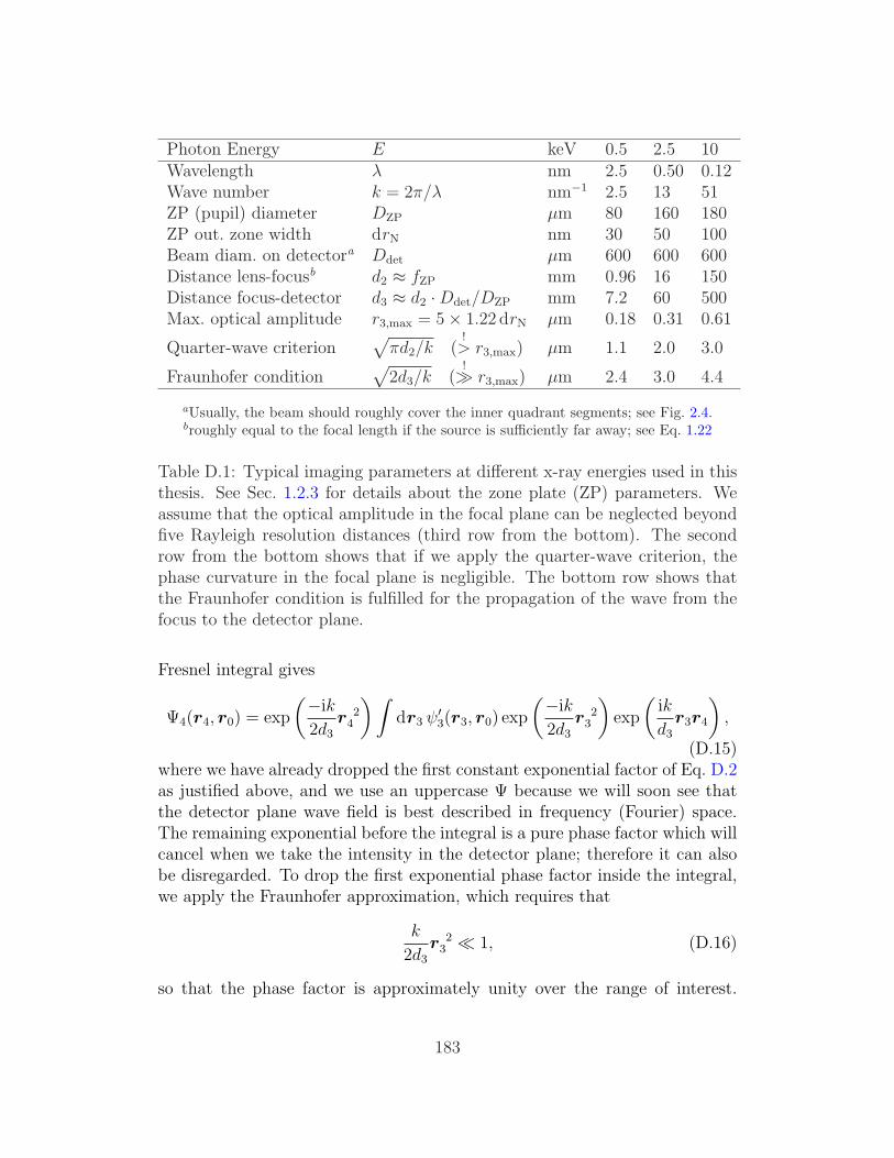
Photon Energy E keV 0.5 2.5 10Wavelength λ nm 2.5 0.50 0.12Wave number k = 2π/λ nm−1 2.5 13 51ZP (pupil) diameter DZP µm 80 160 180ZP out. zone width drN nm 30 50 100Beam diam. on detectora Ddet µm 600 600 600Distance lens-focusb d2 ≈ fZP mm 0.96 16 150Distance focus-detector d3 ≈ d2 ·Ddet/DZP mm 7.2 60 500Max. optical amplitude r3,max = 5× 1.22 drN µm 0.18 0.31 0.61
Quarter-wave criterion√
πd2/k (!> r3,max) µm 1.1 2.0 3.0
Fraunhofer condition√
2d3/k (!À r3,max) µm 2.4 3.0 4.4
aUsually, the beam should roughly cover the inner quadrant segments; see Fig. 2.4.broughly equal to the focal length if the source is sufficiently far away; see Eq. 1.22
Table D.1: Typical imaging parameters at different x-ray energies used in thisthesis. See Sec. 1.2.3 for details about the zone plate (ZP) parameters. Weassume that the optical amplitude in the focal plane can be neglected beyondfive Rayleigh resolution distances (third row from the bottom). The secondrow from the bottom shows that if we apply the quarter-wave criterion, thephase curvature in the focal plane is negligible. The bottom row shows thatthe Fraunhofer condition is fulfilled for the propagation of the wave from thefocus to the detector plane.
Fresnel integral gives
Ψ4(r4, r0) = exp
(−ik
2d3
r 24
) ∫dr3 ψ′3(r3, r0) exp
(−ik
2d3
r 23
)exp
(ik
d3
r3r4
),
(D.15)where we have already dropped the first constant exponential factor of Eq. D.2as justified above, and we use an uppercase Ψ because we will soon see thatthe detector plane wave field is best described in frequency (Fourier) space.The remaining exponential before the integral is a pure phase factor which willcancel when we take the intensity in the detector plane; therefore it can alsobe disregarded. To drop the first exponential phase factor inside the integral,we apply the Fraunhofer approximation, which requires that
k
2d3
r 23 ¿ 1, (D.16)
so that the phase factor is approximately unity over the range of interest.
183

This limits the region in the focal plane which is allowed to contribute to thedetector plane wave field:
r3 ¿√
2d3
k, (D.17)
where r3 = |r3|. Again, we compare this to r3,max, the five Rayleigh resolutiondistances beyond which we assume the wave field in the focal plane to benegligible. The bottom row in Table D.1 shows that the condition is fulfilledin all cases relevant in this thesis work.
In the second exponential factor inside the integral of Eq. D.15, we againsubstitute k = 2π/λ and define spatial frequency coordinates f 4 = r4/(λd3)as in Eq. D.10. Then we can see that within the Fraunhofer approximation,the detector plane wave field is simply the inverse Fourier transform of theexit wave field of the specimen, or
Ψ4(f 4, r0) =
∫dr3 ψ′3(r3, r0) exp(2πir3f 4), (D.18)
whereby we have proven Eq. 4.4. At this point, let us drop the numericalsubscripts for planes 1 through 4 in the optical system, because it should beclear from the context which plane a certain quantity refers to.
In the following, we will make use of the short hand notation of FT andFT−1 for forward and inverse Fourier transforms (see Appendix B). UsingEqs. D.13 and D.14, we can rewrite Eq. D.18 as
Ψ(f , r0) =
∫dr p(r − r0) h(r) exp(2πirf)
= FT−1p(r − r0) h(r)= FT−1p(r − r0) ⊗f FT−1h(r)=
(FT−1p(r) exp(2πir0f)
)⊗f FT−1h(r)=
(FT−1FT−1P (f) exp(2πir0f)
)⊗f
(FT−1FT−1H(f))
= (P (−f) exp(2πir0f))⊗f H(−f), (D.19)
which reproduces Eq. 4.5. In this derivation, we have used the convolution,shift and symmetry theorems of Fourier transforms (see Appendix B). Fur-thermore, H(f) = FTh(r) and P (f) = FTp(r). By using Eq. B.6, we
184
can write out the convolution as integral, or
Ψ(f , r0) =
∫df 1 P (−f − f 1) exp[2πir0(f + f 1)] H(f 1). (D.20)
We now measure the intensity of this wave field with a detector with aresponse function R(f), so that the image recorded by that detector becomes
s(r0) =
∫df R(f) |Ψ(f , r0)|2 (D.21)
(see Eq. 4.6), where the scan displacement coordinate r0 turns into the imagecoordinate as expected.
D.1.2 Large-area Detector: Incoherent Imaging
Let us now prove the results of Sec. 4.1.3. If R(f) = 1 over the whole detectorplane, then
s(r0) =
∫df |Ψ(f , r0)|2
=
∫df
∫dr1 p(r1 − r0) h(r1) exp(2πir1f) ×
×∫
dr2 p∗(r2 − r0) h∗(r2) exp(−2πir2f)
=
∫dr1
∫dr2 p(r1 − r0) p∗(r2 − r0) h(r1) h(r2)×
×∫
df exp(−2πi(r2 − r1)f)︸ ︷︷ ︸
∆(r2−r1)
. (D.22)
We recognize the integral over f as a Dirac delta function (see Sec. B.6), sothat we can perform the integral over r2:
s(r0) =
∫dr1 p(r1 − r0) p∗(r1 − r0) h(r1) h∗(r1)
=
∫dr1 |p(r1 − r0)|2 |h(r1)|2
= |p(r)|2 ?r |h(r)|2 , (D.23)
where ? denotes the crosscorrelation. As noted in Sec. 4.1.3, for a symmetricalpupil the crosscorrelation is equivalent to a convolution, so that we have proven
185

Eq. 4.8.
D.1.3 Point Detector: Coherent Imaging
For a point detector, the detector response can be described by a Dirac delta-function, or R(f) = ∆(f). The image is then given by
s(r0) =
∫df ∆(f) |Ψ(f , r0)|2
=
∫df ∆(f)
∫dr1 p(r1 − r0) h(r1) exp(2πir1f) ×
×∫
dr2 p∗(r2 − r0) h∗(r2) exp(−2πir2f)
=
∫dr1 p(r1 − r0) h(r1)
∫dr2 p∗(r2 − r0) h∗(r2)×
×∫
df ∆(f) exp(−2πi(r2 − r1)f)︸ ︷︷ ︸
=1
=
∣∣∣∣∫
dr p(r − r0) h(r)
∣∣∣∣2
=
∣∣∣∣p(r) ?r h(r)
∣∣∣∣2
. (D.24)
Again, for a symmetrical pupil function P we can use the convolution insteadof the correlation, so that we have proven Eq. 4.11.
D.1.4 Segmented Detector: Partially Coherent Imaging
If we use a segmented detector to measure the image intensity, where individualsegments denoted by the subscript k have response functions Rk(f), the imagerecorded by segment k is
sk(r0) =
∫df Rk(f) |Ψ(f , r0)|2 (D.25)
(compare Eq. D.21). The detector response Rk(f) will be set to one withinthe sensitive area of the detector, and zero otherwise. Let us first expand |Ψ|2
186

from Eq. D.20 into ΨΨ∗, which gives
|Ψ(f , r0)|2 =
∫df 1 P (−f − f 1) H(f 1) exp[2πir0(f + f 1)] ×
×∫
df 2 P ∗(−f − f 2) H∗(f 2) exp[−2πir0(f + f 2)]
=
∫df 1
∫df 2 P (−f − f 1) P ∗(−f − f 2) ×
×H(f 1) H∗(f 2) exp[2πir0(f 1 − f 2)]. (D.26)
Now we take the Fourier transform of Eq. D.25,
Sk(f 0) =
∫dr0 sk(r0) exp(−2πir0f 0), (D.27)
and insert from Eqs. D.25 and D.26:
Sk(f 0) =
∫dr0
∫df Rk(f)
∫df 1
∫df 2 P (−f − f 1) P ∗(−f − f 2)×
×H(f 1) H∗(f 2) exp[−2πir0(f 2 − (f 1 − f 0))]. (D.28)
Now we can replace
∫dr0 exp[−2πir0(f 2 − (f 1 − f 0))] = ∆(f 2 − (f 1 − f 0)), (D.29)
where ∆(f) is again the Dirac delta-function (see Sec. B.6). Then we canperform the integral over f 2:
∫df 2 F (f 2) ∆(f 2 − (f 1 − f 0)) = F (f 1 − f 0) (D.30)
(see Eq. B.11), where F (f 2) includes all the other remaining terms. Eq. D.28then becomes
Sk(f 0) =
∫df Rk(f)
∫df 1 P (−f − f 1) P ∗(−f − f 1 + f 0)×
× H(f 1) H∗(f 1 − f 0). (D.31)
187
We can identify the integral over f 1 as convolution integral (see Eq. B.6), sothat we get
Sk(f 0) =
∫df Rk(f) (P (−f) · P ∗(−f − f 0))⊗f (H(−f) ·H∗(−f − f 0)) ,
(D.32)which reproduces Eq. 4.14.
In the weak specimen approximation, we write the Fourier transform ofthe specimen as
H(f) = ∆(f) + Hr(f) + i Hi(f) (D.33)
as described in Sec. 4.1.6 (Eq. 4.18). The product of specimen functions inEq. D.31 can then be written as
H(f 1) ·H∗(f 1 − f 0) = ∆(f 1) ·∆(f 1 − f 0) +
+ ∆(f 1) [H∗r (f 1 − f 0)− i H∗
i (f 1 − f 0)] +
+ ∆(f 1 − f 0) [Hr(f 1) + i Hi(f 1)] +
+O(H 2r,i ). (D.34)
Here, we assume that terms on the order of H 2r,i are small compared to the
delta-function terms and can be neglected. Within this weak specimen ap-proximation, we can rewrite Eq. D.31 as
Sk(f 0) =
∫df Rk(f)
∫df 1 P (−f − f 1) P ∗(−f − f 1 + f 0)×
× ∆(f 1) ∆(f 1 − f 0) +
+
∫df Rk(f)
∫df 1 P (−f − f 1) P ∗(−f − f 1 + f 0)×
× ∆(f 1) [H∗r (f 1 − f 0)− i H∗
i (f 1 − f 0)] +
+
∫df Rk(f)
∫df 1 P (−f − f 1) P ∗(−f − f 1 + f 0)×
× ∆(f 1 − f 0) [Hr(f 1) + i Hi(f 1)] . (D.35)
In each of the three summands in this equation, we can perform the integralover the delta function, where in the first term we choose to integrate over
188

the first one of the two delta functions (for the final result, it does not matterwhich one we integrate over). We then get
Sk(f 0) =
∫df Rk(f) P (−f) P ∗(−f + f 0) ∆(f 0) +
+
∫df Rk(f) P (−f) P ∗(−f + f 0) [H∗
r (−f 0)− i H∗i (−f 0)] +
+
∫df Rk(f) P (−f − f 0) P ∗(−f) [Hr(f 0) + i Hi(f 0)] (D.36)
Since hr,i are purely real functions, their Fourier transforms are conjugatesymmetric, or Hr,i(f 0) = H∗
r,i(−f 0) (also see Table B.2). Now let us definethe bilinear transfer functions
Ck(m,n, f 0) =
∫df Rk(f) P (mf 0 − f) P ∗(nf 0 − f), (D.37)
so that the final result for the image recorded by detector segment k becomes
Sk(f 0) = ∆(f 0) Ck(0, 0,f 0) +
+ Ck(0, 1,f 0) [Hr(f 0)− i Hi(f 0)] +
+ Ck(−1, 0, f 0) [Hr(f 0) + i Hi(f 0)]
= ∆(f 0) Ck(0, 0,f 0) +
+ Hr(f 0) [Ck(−1, 0,f 0) + Ck(0, 1,f 0)] +
+ i Hi(f 0) [Ck(−1, 0,f 0)− Ck(0, 1,f 0)] , (D.38)
whereby we have proven Eq. 4.19. For the first term of this sum, we havetaken advantage of the multiplication with the delta function, so that only thef 0 = 0 component is of interest. Hence,
Ck(m,n, f 0 =0) =
∫df Rk(f) |P (−f)|2 (D.39)
is independent of m and n, and
∆(f 0) · Ck(0, 1,f 0) = ∆(f 0) · Ck(−1, 0,f 0) = ∆(f 0) · Ck(0, 0,f 0). (D.40)
Note that Ck(0, 0,f 0) is constant for all f 0 and represents the total intensitymeasured by detector segment k in absence of a specimen.
189
By defining the contrast transfer functions for the real and imaginary partsof the specimen
T (k)r (f 0) = Ck(−1, 0,f 0) + Ck(0, 1,f 0)
T(k)i (f 0) = Ck(−1, 0,f 0)− Ck(0, 1, f 0), (D.41)
we can write
Sk(f 0) = ∆(f 0) Ck(0, 0,f 0) + Hr(f 0) T (k)r (f 0) + i Hi(f 0) T
(k)i (f 0). (D.42)
D.2 Transfer Function Symmetries
For a better understanding of the bilinear and contrast transfer functions, andas a preparation for Sec. D.3, we want to study some symmetry properties ofthe transfer functions which were introduced above. From the definition of thebilinear transfer functions in Eq. D.37,
Ck(0, 1,f 0) =
∫df Rk(f) P (−f) P ∗(f 0 − f)
= Ck(0,−1,−f 0)
=
[∫df Rk(f) P ∗(−f) P (f 0 − f)
]∗
= C∗k(1, 0,f 0)
= C∗k(−1, 0,−f 0), (D.43)
where we have used the fact that the detector response functions will alwaysbe real, so that Rk(f) = R∗
k(f). Consequently (compare Eq. D.41),
T (k)r (f 0) = Ck(−1, 0,f 0) + Ck(0, 1,f 0)
= Ck(−1, 0,f 0) + C∗k(−1, 0,−f 0) (D.44)
and
T (k)∗r (−f 0) = C∗
k(−1, 0,−f 0) + Ck(−1, 0,f 0)
= T (k)r (f 0). (D.45)
190

Similarly for the imaginary part transfer function,
T(k)i (f 0) = Ck(−1, 0, f 0)− Ck(0, 1, f 0)
= Ck(−1, 0, f 0)− C∗k(−1, 0,−f 0) (D.46)
and
T(k)∗i (−f 0) = C∗
k(−1, 0,−f 0)− Ck(−1, 0,f 0)
= −T(k)i (f 0). (D.47)
In words, the real part contrast transfer functions are conjugate symmetric,while the imaginary part transfer functions are conjugate antisymmetric.
If the pupil P is real, then the contrast transfer functions will be realas well (the detector response is always real). In this case, the real parttransfer functions are symmetric, and the imaginary part transfer functionsare antisymmetric, which we have stated already in Sec. 4.2.4.
Let us now study the case where the detector configuration is symmetric,that is, each detector segment k has an opposite segment k such that Rk(f) =Rk(−f). Then,
Ck(−1, 0,f 0) =
∫df Rk(f) P (−f 0 − f) P ∗(−f).
Now transform the variable f → −f ; the integral over the whole frequencyplane will stay the same:
Ck(−1, 0,f 0) =
∫df Rk(f) P (−f 0 + f) P ∗(f).
If the pupil is centrosymmetric such that P (f) = P (−f), then
Ck(−1, 0,f 0) =
∫df Rk(f) P (f 0 − f) P ∗(−f)
= Ck(−1, 0,−f 0). (D.48)
191

The contrast transfer functions then become
T (k)r (f 0) = Ck(−1, 0,f 0) + C ∗
k(−1, 0,−f 0)
= Ck(−1, 0,−f 0) + C∗k(−1, 0,f 0)
= T (k)r (−f 0)
= T (k)∗r (f 0) (D.49)
and
T(k)i (f 0) = Ck(−1, 0,f 0)− C ∗
k(−1, 0,−f 0)
= Ck(−1, 0,−f 0)− C∗k(−1, 0,f 0)
= T(k)i (−f 0)
= −T(k)∗i (f 0). (D.50)
Therefore, we can say that for opposite detector segments, the real part trans-fer functions are complex conjugates and the imaginary part transfer functionsare negated and complex conjugates (if the pupil is symmetric). If the pupil isreal, then the real part transfer functions are the same for opposite segments,and the imaginary part transfer functions are opposite in sign, as stated inSec. 4.2.4.
Finally, if we have an individual segment k which is symmetrical about theorigin such that Rk(f) = Rk(−f), and the pupil is also symmetrical,
C∗k(−1, 0,−f 0) =
∫df Rk(f) P (f 0 − f) P ∗(−f)
[use P (f) = P (−f)]
=
∫df Rk(f) P (−f 0 + f) P ∗(f)
[f → −f ; and use Rk(f) = Rk(−f)]
=
∫df Rk(f) P (−f 0 − f) P ∗(−f)
= Ck(−1, 0, f 0). (D.51)
192
Comparing with Eq. D.46, we see that the imaginary part transfer function iszero in this case.
D.3 Fourier Filter Reconstruction
To derive the reconstruction formula, we start with the assumption of Eq. 4.25:
H(f) =∑
k
Wk(f) Sk(f), (D.52)
and we have to find the Fourier filtering functions Wk. We have dropped thesubscript 0 from the frequency variable because all quantities (specimen, pupiland detector response) must be calculated in the same frequency space.
Now let us define the root mean square (rms) error of the reconstructionas (Eq. 4.26)
ε =
∫df
⟨∣∣∣H(f)−H(f)∣∣∣2⟩
︸ ︷︷ ︸F
, (D.53)
which has to be minimized for an optimal reconstruction. The brackets 〈〉indicate an expectation value, which averages over many measurements of thenoisy data Sk. The integrand F of Eq. D.53 is real and greater than or equalto zero for all spatial frequencies f , so that we can disregard the frequencydependence and the integral. Let us first write out the integrand:
F ≡⟨∣∣∣H −H
∣∣∣2⟩
=
⟨∣∣∣∣∣∑
l
Wl Sl −H
∣∣∣∣∣
2⟩
=
⟨(∑
l
Wl Sl −H
)(∑m
W ∗m S∗m −H∗
)⟩(D.54)
To minimize the reconstruction error, let us decompose the functions Wk intotheir real and imaginary parts W
(r,i)k and set the partial derivative of F with
193

respect to each of them to zero:
∂F
∂W(r)k
=
⟨Sk
(∑m
W ∗m S∗m −H∗
)+ S∗k
(∑
l
Wl Sl −H
)⟩
=
⟨[S∗k
(∑m
Wm Sm −H
)]∗+ S∗k
(∑
l
Wl Sl −H
)⟩
=
⟨2 Re
S∗k
(∑
l
Wl Sl −H
)⟩(D.55)
∂F
∂W(i)k
=
⟨i Sk
(∑m
W ∗m S∗m −H∗
)− i S∗k
(∑
l
Wl Sl −H
)⟩
=
⟨i
[S∗k
(∑m
Wm Sm −H
)]∗− i S∗k
(∑
l
Wl Sl −H
)⟩
=
⟨−2i Im
S∗k
(∑
l
Wl Sl −H
)⟩. (D.56)
To minimize F , we set both of these partial derivatives to zero (for all k),which means that the real and imaginary part of the expression in braces must be zero, or
⟨S∗k
(∑
l
Wl Sl −H
)⟩= 0 for all k, (D.57)
whereby we have proven Eq. 4.27. To solve this equation for the Wk, wesubstitute for Sk the weak specimen approximation of Eq. D.42. At first wewill disregard the f = 0 component and therefore the ∆-term (it will be takeninto account below); furthermore we will add a term Nk(f) which describesthe spectral noise on detector segment k:
Sk(f) = Hr(f) T (k)r (f) + i Hi(f) T
(k)i (f) + Nk(f) for f 6= 0 and all k.
(D.58)Also, we insert the Fourier transform of the specimen function from Eq. D.33,where again we omit the ∆-term because we disregard the zero frequencycomponent. Plugging these into Eq. D.57, we get (omitting the frequency
194

dependence for simplicity)
0 =
⟨ (H∗
r T (k)∗r − i H∗
i T(k)∗i + N∗
k
)×
×( ∑
l
Wl
(Hr T (l)
r + i Hi T(l)i + Nl
)− (Hr + i Hi)
)⟩
for f 6= 0 and all k. (D.59)
Expanding all the parenthesis gives
0 =
⟨|Hr|2 T (k)∗
r
∑
l
Wl T(l)r
⟩+ i
⟨H∗
r T (k)∗r
∑
l
Wl Hi T(l)i
⟩
︸ ︷︷ ︸=0 (Hr, Hi uncorrelated)
+
+
⟨H∗
r T (k)∗r
∑
l
Wl Nl
⟩
︸ ︷︷ ︸=0 (N , H uncorr.)
−⟨|Hr|2 T (k)∗
r
⟩− i
⟨Hi H
∗r T (k)∗
r
⟩
︸ ︷︷ ︸=0 (Hr, Hi uncorr.)
−
− i
⟨H∗
i T(k)∗i
∑
l
Wl Hr T (l)r
⟩
︸ ︷︷ ︸=0 (Hr, Hi uncorr.)
+
⟨|Hi|2 T
(k)∗i
∑
l
Wl T(l)i
⟩−
− i
⟨H∗
i T(k)∗i
∑
l
Wl Nl
⟩
︸ ︷︷ ︸=0 (N , H uncorr.)
+i
⟨Hr H∗
i T(k)∗i
⟩
︸ ︷︷ ︸=0 (Hr, Hi uncorr.)
−⟨|Hi|2 T
(k)∗i
⟩+
+
⟨N∗
k
∑
l
Wl Hr T (l)r
⟩
︸ ︷︷ ︸=0 (N , H uncorr.)
+i
⟨N∗
k
∑
l
Wl Hi T(l)i
⟩
︸ ︷︷ ︸=0 (N , H uncorr.)
+
+
⟨N∗
k
∑
l
Wl Nl
⟩
︸ ︷︷ ︸=0 for l 6=k (Nl, Nk uncorr.)
−⟨
Hr N∗k
⟩
︸ ︷︷ ︸=0 (H, N uncorr.)
−i
⟨Hi N
∗k
⟩
︸ ︷︷ ︸=0 (H, N uncorr.)
for f 6= 0 and all k. (D.60)
195

If we assume that the noise is uncorrelated between different detector seg-ments, that the noise is uncorrelated with the specimen function (this is thedefinition of noise!), and that the real and imaginary parts of the specimenare uncorrelated, we can disregard many of the cross terms as noted in theequation. We can also disregard the expectation value for all terms except theremaining noise term. Rearranging the remaining terms gives
0 = |Hr|2 T (k)∗r
(∑
l
Wl T(l)r − 1
)+
+ |Hi|2 T(k)∗i
(∑
l
Wl T(l)i − 1
)+ Wk
⟨|Nk|2⟩
for f 6= 0 and all k.
(D.61)
If we multiply this equation by T(k)r / 〈|Nk|2〉 and sum over all k, we get
0 = |Hr|2(∑
l
Wl T(l)r − 1
) ∑
k
∣∣∣T (k)r
∣∣∣2
⟨|Nk|2⟩ +
+ |Hi|2(∑
l
Wl T(l)i − 1
) ∑
k
T(k)∗i T
(k)r⟨|Nk|2⟩ +
∑
k
Wk T (k)r for f 6= 0.
(D.62)
Now let us define the following quantities:
β(k)r =
⟨|Nk|2⟩
|Hr|2β
(k)i =
⟨|Nk|2⟩
|Hi|2(D.63)
D(r) = 1 +∑
k
∣∣∣T (k)r
∣∣∣2
β(k)r
D(i) = 1 +∑
k
∣∣∣T (k)i
∣∣∣2
β(k)i
(D.64)
D(r,i) =∑
k
T(k)∗r T
(k)i
β(k)r
D(i,r) =∑
k
T(k)∗i T
(k)r
β(k)i
(D.65)
With those definitions, Eq. D.62 becomes
D(r)∑
l
Wl T(l)r + D(i,r)
∑
l
Wl T(l)i = D(r) + D(i,r) − 1 for f 6= 0. (D.66)
196

In the same way, we can multiply Eq. D.61 by T(k)i / 〈|Nk|2〉 and sum over all
k to obtain
D(i)∑
l
Wl T(l)i + D(r,i)
∑
l
Wl T(l)r = D(i) + D(r,i) − 1 for f 6= 0. (D.67)
Eqs. D.66 and D.67 constitute a set of linear equations for∑
l Wl T(l)r and∑
l Wl T(l)i , which can be solved to give
∑
l
Wl T(l)r = 1 +
D(i,r) −D(i)
D(r) D(i) −D(i,r) D(r,i)
∑
l
Wl T(l)i = 1 +
D(r,i) −D(r)
D(r) D(i) −D(i,r) D(r,i)
for f 6= 0. (D.68)
Substituting those back into Eq. D.61 gives the general solution for the recon-struction filters:
Wk =D(i) −D(i,r)
D(r) D(i) −D(i,r) D(r,i)
T(k)∗r
β(k)r
+D(r) −D(r,i)
D(r) D(i) −D(i,r) D(r,i)
T(k)∗i
β(k)i
for f 6= 0 and all k. (D.69)
For a further simplification of the reconstruction filters, we make use of thetransfer function symmetry relations of Sec. D.2. Let us assume that the pupilfunction is real and centrosymmetric, and that each detector segment has acorresponding opposite segment. We also allow individual segments which aresymmetrical by themselves, like the central segment of our 9 and 10 segmentdetector structures, and like the outer rings of our 8 and 10 segment structures(see Fig. 2.4).
The term D(r,i) of Eq. D.65 consists of a sum over all detector segments.For segments which are symmetrical about the origin by themselves, T
(k)i is
zero as shown at the end of Sec. D.2, so that they do not contribute to thesum. Now let us have a closer look at the contribution of opposite detectorpairs k, k. We assume that both segments show the same noise spectrum, so
that β(k)r,i = β
(k)r,i . Then,
D(r,i) =∑
k,k
T(k)∗r T
(k)i + T
(k)∗r T
(k)i
β(k)r
, (D.70)
197

where the sum is taken over all pairs of opposite detector segments k and k.Using Eqs. D.49 and D.50, we get
D(r,i) =∑
k,k
T(k)∗r T
(k)i − T
(k)r T
(k)∗i
β(k)r
= 0 (D.71)
if the transfer functions are real (that is, the pupil is real). In the sameway, D(i,r) vanishes. This simplifies the reconstruction filters of Eq. D.69significantly to
Wk =T
(k)∗r
D(r) β(k)r
+T
(k)∗i
D(i) β(k)i
for f 6= 0 and all k. (D.72)
If we assume that the noise is the same on all segments (β(k)r,i = βr,i), we can
substitute D(r) and D(i) back from Eq. D.64 to get
Wk =T
(k)∗r
∑l
∣∣∣T (l)r
∣∣∣2
+ βr
+T
(k)∗i
∑l
∣∣∣T (l)i
∣∣∣2
+ βi
for f 6= 0 and all k, (D.73)
whereby we have proven Eq. 4.29.For the zero frequency term, let us remember that Ck(m,n, f = 0) is a
constant independent of m and n (see Eq. D.39). Consequently,
Ck(0, 0,f =0) =1
2T (k)
r (f =0) (D.74)
and
T(k)i (f =0) = 0 (D.75)
(compare Eq. D.41). If we assume that Hr(f = 0) is negligible compared tothe delta-function term in Eq. D.42 (which was also required for the weak-specimen approximation of Eq. D.34), we can write
Sk(0) = ∆(0)T
(k)r (0)
2. (D.76)
198
In Eq. 4.31, we have claimed that
Wk(0) =2 T
(k)∗r (0)
∑l
∣∣∣T (l)r (0)
∣∣∣2
+ βr(0). (D.77)
If we assume that βr(0) = 0, that is, the noise has an average of zero,1 we cansubstitute Eqs. D.76 and D.77 into Eq. D.52 to find that
H(0) = ∆(0), (D.78)
which is consistent with the specimen function of Eq. D.33 and therefore provesEq. D.77 (again assuming that Hr(0) is negligible against the delta-functionterm). The imaginary part of the specimen function at f = 0 is irrelevant,because
• due to the zero contrast transfer at f = 0, we could not trust anyreconstructed value anyway; and
• the f = 0 value of the specimen Fourier transform constitutes onlya constant phase offset across the whole image, and we can easily (infact, we have to) normalize the final result for a zero phase shift in thebackground region.
1Remember that the zero frequency term in a Fourier transform or spectrum denotesthe total value (or, with appropriate scaling, the average value) of the corresponding realspace quantity; see Sec. B.1.
199

Bibliography
[1] D. Attwood. Soft X-rays and Extreme Ultraviolet Radiation. CambridgeUniversity Press, 1999.
[2] W. Yun and G. Ice. X-ray microbeam and microscopy techniques withhard x-rays. In Mills [12], chapter 4.
[3] A. A. Markowicz. X-ray physics. In Van Grieken and Markowicz [4],chapter 1.
[4] R. E. Van Grieken and A. A. Markowicz, editors. Handbook of X-raySpectrometry, volume 14 of Practical Spectroscopy. Marcel Dekker, Inc.,1993.
[5] J. Kirz, C. Jacobsen, and M. Howells. Soft x-ray microscopes and theirbiological applications. Quarterly Reviews of Biophysics, 28(1):33–130,1995. Also available as Lawrence Berkeley Laboratory report LBL-36371.
[6] A. H. Compton. A quantum theory of the scattering of x-rays by lightelements. Physical Review, 21(5):483–502, 1923.
[7] A. Thompson et al. X-ray data booklet. Lawrence Berkeley NationalLaboratory, University of California, Berkeley, CA 94720, January 2001.Online at http://xdb.lbl.gov/.
[8] B. L. Henke. Low energy x-ray interactions: photoionization, scattering,specular and Bragg reflection. In D. T. Attwood and B. L. Henke, editors,Low Energy X-ray Diagnostics, volume 75, pages 146–155, New York,1981. American Institute of Physics. Monterey, 1981.
[9] B. L. Henke, E. M. Gullikson, and J. C. Davis. X-ray interactions: Pho-toabsorption, scattering, transmission, and reflection at E=50–30,000 eV,Z=1–92. Atomic Data and Nuclear Data Tables, 54:181–342, 1993.
[10] M. O. Krause. Atomic radiative and radiationless yields for K and L shells.Journal of Physical and Chemical Reference Data, 8:307–327, 1979.
200
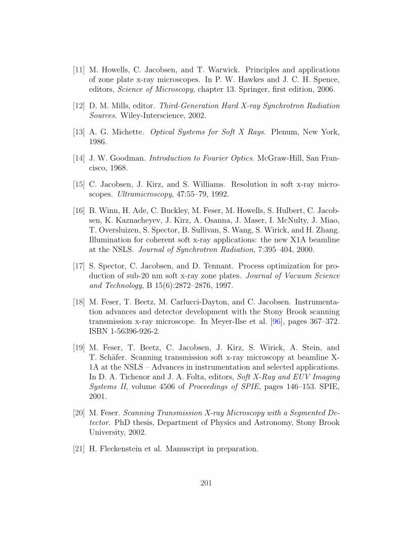
[11] M. Howells, C. Jacobsen, and T. Warwick. Principles and applicationsof zone plate x-ray microscopes. In P. W. Hawkes and J. C. H. Spence,editors, Science of Microscopy, chapter 13. Springer, first edition, 2006.
[12] D. M. Mills, editor. Third-Generation Hard X-ray Synchrotron RadiationSources. Wiley-Interscience, 2002.
[13] A. G. Michette. Optical Systems for Soft X Rays. Plenum, New York,1986.
[14] J. W. Goodman. Introduction to Fourier Optics. McGraw-Hill, San Fran-cisco, 1968.
[15] C. Jacobsen, J. Kirz, and S. Williams. Resolution in soft x-ray micro-scopes. Ultramicroscopy, 47:55–79, 1992.
[16] B. Winn, H. Ade, C. Buckley, M. Feser, M. Howells, S. Hulbert, C. Jacob-sen, K. Kaznacheyev, J. Kirz, A. Osanna, J. Maser, I. McNulty, J. Miao,T. Oversluizen, S. Spector, B. Sullivan, S. Wang, S. Wirick, and H. Zhang.Illumination for coherent soft x-ray applications: the new X1A beamlineat the NSLS. Journal of Synchrotron Radiation, 7:395–404, 2000.
[17] S. Spector, C. Jacobsen, and D. Tennant. Process optimization for pro-duction of sub-20 nm soft x-ray zone plates. Journal of Vacuum Scienceand Technology, B 15(6):2872–2876, 1997.
[18] M. Feser, T. Beetz, M. Carlucci-Dayton, and C. Jacobsen. Instrumenta-tion advances and detector development with the Stony Brook scanningtransmission x-ray microscope. In Meyer-Ilse et al. [96], pages 367–372.ISBN 1-56396-926-2.
[19] M. Feser, T. Beetz, C. Jacobsen, J. Kirz, S. Wirick, A. Stein, andT. Schafer. Scanning transmission soft x-ray microscopy at beamline X-1A at the NSLS – Advances in instrumentation and selected applications.In D. A. Tichenor and J. A. Folta, editors, Soft X-Ray and EUV ImagingSystems II, volume 4506 of Proceedings of SPIE, pages 146–153. SPIE,2001.
[20] M. Feser. Scanning Transmission X-ray Microscopy with a Segmented De-tector. PhD thesis, Department of Physics and Astronomy, Stony BrookUniversity, 2002.
[21] H. Fleckenstein et al. Manuscript in preparation.
201
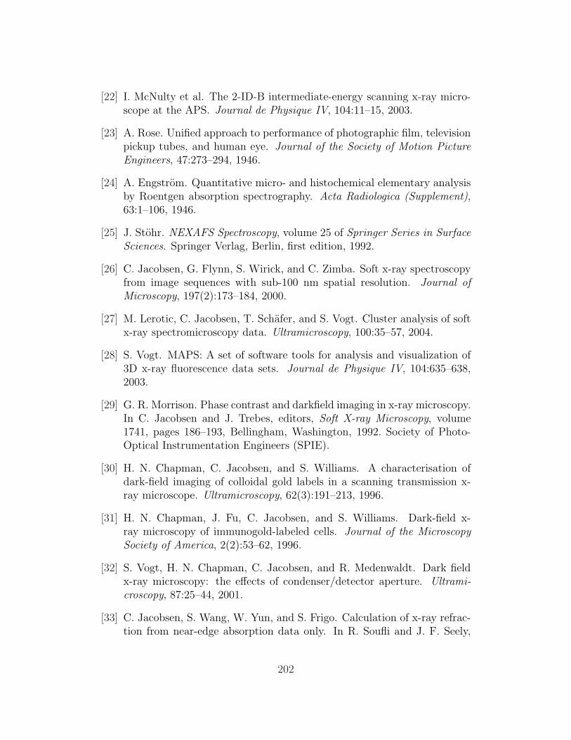
[22] I. McNulty et al. The 2-ID-B intermediate-energy scanning x-ray micro-scope at the APS. Journal de Physique IV, 104:11–15, 2003.
[23] A. Rose. Unified approach to performance of photographic film, televisionpickup tubes, and human eye. Journal of the Society of Motion PictureEngineers, 47:273–294, 1946.
[24] A. Engstrom. Quantitative micro- and histochemical elementary analysisby Roentgen absorption spectrography. Acta Radiologica (Supplement),63:1–106, 1946.
[25] J. Stohr. NEXAFS Spectroscopy, volume 25 of Springer Series in SurfaceSciences. Springer Verlag, Berlin, first edition, 1992.
[26] C. Jacobsen, G. Flynn, S. Wirick, and C. Zimba. Soft x-ray spectroscopyfrom image sequences with sub-100 nm spatial resolution. Journal ofMicroscopy, 197(2):173–184, 2000.
[27] M. Lerotic, C. Jacobsen, T. Schafer, and S. Vogt. Cluster analysis of softx-ray spectromicroscopy data. Ultramicroscopy, 100:35–57, 2004.
[28] S. Vogt. MAPS: A set of software tools for analysis and visualization of3D x-ray fluorescence data sets. Journal de Physique IV, 104:635–638,2003.
[29] G. R. Morrison. Phase contrast and darkfield imaging in x-ray microscopy.In C. Jacobsen and J. Trebes, editors, Soft X-ray Microscopy, volume1741, pages 186–193, Bellingham, Washington, 1992. Society of Photo-Optical Instrumentation Engineers (SPIE).
[30] H. N. Chapman, C. Jacobsen, and S. Williams. A characterisation ofdark-field imaging of colloidal gold labels in a scanning transmission x-ray microscope. Ultramicroscopy, 62(3):191–213, 1996.
[31] H. N. Chapman, J. Fu, C. Jacobsen, and S. Williams. Dark-field x-ray microscopy of immunogold-labeled cells. Journal of the MicroscopySociety of America, 2(2):53–62, 1996.
[32] S. Vogt, H. N. Chapman, C. Jacobsen, and R. Medenwaldt. Dark fieldx-ray microscopy: the effects of condenser/detector aperture. Ultrami-croscopy, 87:25–44, 2001.
[33] C. Jacobsen, S. Wang, W. Yun, and S. Frigo. Calculation of x-ray refrac-tion from near-edge absorption data only. In R. Soufli and J. F. Seely,
202

editors, Optical Constants of Materials for UV to X-ray Wavelengths,volume 5538, pages 5538–03. SPIE, 2004.
[34] N. H. Dekkers and H. de Lang. Differential phase contrast in a STEM.Optik, 41(4):452–456, 1974.
[35] H. Rose. Nonstandard imaging methods in electron microscopy. Ultrami-croscopy, 2:251–267, 1977.
[36] P. W. Hawkes. Half-plane apertures in TEM, split detectors in STEMand ptychography. J. Optics (Paris), 9(4):235–241, 1978.
[37] J. M. Rodenburg and R. H. T. Bates. The theory of super-resolutionelectron microscopy via Wigner-distribution deconvolution. PhilosophicalTransactions of the Royal Society of (London), A 339:521–553, 1992.
[38] H. N. Chapman. Phase-retrieval x-ray microscopy by Wigner-distributiondeconvolution. Ultramicroscopy, 66:153–172, 1996.
[39] H. N. Chapman, C. Jacobsen, and S. Williams. Applications of a CCDdetector in scanning transmission x-ray microscope. Review of ScientificInstruments, 66(2):1332–1334, 1995.
[40] G. R. Morrison and B. Niemann. Differential phase contrast x-ray mi-croscopy. In Thieme et al. [97], pages I–85–I–94.
[41] W. J. Eaton, G. R. Morrison, and N. R. Waltham. Configured detectorsystem for STXM imaging. In Meyer-Ilse et al. [96], pages 452–457. ISBN1-56396-926-2.
[42] G. Morrison, W. J. Eaton, R. Barnett, and P. Charalambous. STXMimaging with a configured detector. pages 547–550.
[43] G. R. Morrison, A. Gianoncelli, B. Kaulich, D. Bacescu, and J. Kovac. Afast-readout CCD system for configured-detector imaging in STXM. InAoki et al. [98], pages 377–379.
[44] U. Wiesemann, J. Thieme, R. Fruke, P. Guttmann, B. Niemann,D. Rudolph, and G. Schmahl. Construction of a scanning transmission X-ray microscope at the undulator U-41 at BESSY II. Nuclear Instrumentsand Methods in Physics Research A, 467-468:861–863, 2001.
[45] E. M. Waddell and J. N. Chapman. Linear imaging of strong phase objectsusing asymmetrical detectors in STEM. Optik, 54:83–96, 1979.
203

[46] G. R. Morrison and J. N. Chapman. A comparison of three differentialphase contrast systems suitable for use in STEM. Optik, 64(1):1–12, 1983.
[47] Y. Kagoshima, K. Shimose, T. Koyama, I. Wada, A. Saikubo, K. Hayashi,Y. Tsusaka, and J. Matsui. Scanning differential-phase-contrast hardX-ray microscopy with wedge absorber detector. Japanese Journal ofApplied Physics, 43(11A):L1449–L1451, 2004.
[48] M. Feser, B. Hornberger, C. Jacobsen, G. De Geronimo, P. Rehak, P. Holl,and L. Struder. Integrating silicon detector with segmentation for scan-ning transmission x-ray microscopy. Nuclear Instruments and Methods inPhysics Research A, 565:841–854, 2006.
[49] J. R. Palmer and G. R. Morrison. Differential phase contrast imagingin the scanning transmission x-ray microscope. In P. H. Bucksbaumand N. M. Ceglio, editors, OSA Proceedings on Short Wavelength Coher-ent Radiation: Generation and Applications, volume 11, pages 141–145,Washington, D. C., 1991. Optical Society of America.
[50] G. Schmahl and D. Rudolph. Proposal for a phase contrast x-ray mi-croscope. In P. C. Cheng and G. J. Jan, editors, X-ray Microscopy: In-strumentation and Biological Applications, pages 231–238, Berlin, 1987.Springer-Verlag.
[51] F. Zernike. Das Phasenkontrastverfahren bei der mikroskopishenBeobachtung. Zeitschrift fur technische Physik, 36:848–851, 1935.
[52] A. Momose. Recent advances in X-ray phase imaging. Japanese Journalof Applied Physics, 44(9A):6355–6367, 2005.
[53] G. R. Morrison. Some aspects of quantitative x-ray microscopy. In ReneBenattar, editor, X-ray Instrumentation in Medicine and Biology, PlasmaPhysics, Astrophysics, and Synchrotron Radiation, volume 1140, pages41–49, Bellingham, Washington, 1989. Society of Photo-Optical Instru-mentation Engineers (SPIE).
[54] F. Polack and D. Joyeux. Soft x-ray interferential scanning microscopy:a feasibility assessment. In V. V. Aristov and A. I. Erko, editors, X-rayMicroscopy IV, pages 432–437, Chernogolovka, Russia, 1994. BogorodskiiPechatnik. ISBN 5-900846-01-6. Proceedings of the 4th InternationalConference, Chernogolovka, Russia, September 20–24, 1993.
204

[55] F. Polack, D. Joyeux, and D. Phalippou. Phase contrast experiments onthe NSLS-X1A scanning microscope. In Thieme et al. [97], pages I–105–109.
[56] D. Joyeux and F. Polack. A wavefront profiler as an insertion device forscanning phase contrast microscopy. In Thieme et al. [97], pages II–201–205.
[57] B. Kaulich, F. Polack, U. Neuhausler, J. Susini, Enzo di Fabrizio, andT. Wilhein. Diffracting aperture based differential phase contrast forscanning x-ray microscopy. Opt Express, 10(20):1112–1117, October 2002.
[58] B. Kaulich, T. Wilhein, E. Di Fabrizio, F. Romanato, M. Altissimo,S. Cabrini, B. Fayard, and J. Susini. Differential interference contrastx-ray microscopy with twin zone plates. J. Opt. Soc. Am. A, 19(4):797–806, 2002.
[59] M. Feser, C. Jacobsen, P. Rehak, G. DeGeronimo, P. Holl, and L. Struder.Novel integrating solid state detector with segmentation for scanningtransmission soft x-ray microscopy. In I. McNulty, editor, X-ray micro-and nano-focusing: applications and techniques II, volume 4499, pages117–125, Bellingham, Washington, 2001. Society of Photo-Optical Instru-mentation Engineers (SPIE).
[60] W. Chen, G. De Geronimo, Z. Li, P. O’Connor, V. Radeka, P. Rehak,G. C. Smith, and B. Yu. Active pixel sensors on high resistivity siliconand their readout. Nuclear Science Symposium Conference Record, 2001IEEE, 2:980–985, 2001.
[61] G. Lutz. Silicon drift and pixel devices for X-ray imaging and spec-troscopy. Journal of Synchrotron Radiation, 13:99–109, 2006.
[62] A. Ercan, M. W. Tate, and S. M. Gruner. Analog pixel array detectors.Journal of Synchrotron Radiation, 13:110–119, 2006.
[63] C. Broennimann et al. The PILATUS 1M detector. Journal of Syn-chrotron Radiation, 13:120–130, 2006.
[64] Glenn F. Knoll. Radiation detection and measurement. John Wiley &Sons, Inc., first edition, 1979.
[65] M. Feser, M. Carlucci-Dayton, C. J. Jacobsen, J. Kirz, U. Neuhausler,G. Smith, and B. Yu. Applications and instrumentation advances withthe Stony Brook scanning transmission x-ray microscope. In I. McNulty,
205

editor, X-ray microfocusing: applications and techniques, volume 3449,pages 19–29, Bellingham, Washington, 1998. Society of Photo-OpticalInstrumentation Engineers (SPIE).
[66] J. Maser et al. The hard x-ray nanoprobe beamline at the AdvancedPhoton Source. In Aoki et al. [98], pages 26–29.
[67] L. Struder et al. The european photon imaging camera on XMM-newton:The pn-CCD camera. Astron. Astrophys., 365:L18–L26, 2001.
[68] P. Horowitz and W. Hill. The Art of Electronics. Cambridge UniversityPress, 2nd edition, 1989.
[69] W. H. Press, S. A. Teukolsky, W. T. Vetterling, and B. P. Flannery.Numerical Recipes in C. Cambridge University Press, 2nd edition, 1992.
[70] R. M. Glaeser. Limitations to significant information in biological electronmicroscopy as a result of radiation damage. Journal of UltrastructureResearch, 36:466–482, 1971.
[71] D. Sayre, J. Kirz, R. Feder, D. M. Kim, and E. Spiller. Transmissionmicroscopy of unmodified biological materials: Comparative radiationdosages with electrons and ultrasoft x-ray photons. Ultramicroscopy, 2:337–341, 1977.
[72] B. S. Twining, S. B. Baines, N. S. Fisher, J. Maser, S. Vogt, C. Jacob-sen, A. Tovar-Sanchez, and S. A. Sanudo-Wilhelmy. Quantifying traceelements in individual aquatic protist cells with a synchrotron x-ray flu-orescence microprobe. Analytical Chemistry, 75:3806–3816, 2003.
[73] W. H. Southwell. Wave-front estimation from wave-front slope measure-ments. Journal of the Optical Society of America, 70(8):998–1006, 1980.
[74] C. Kottler, C. David, F. Pfeiffer, and O. Bunk. A two-directional approachfor grating based differential phase contrast imaging using hard x-rays.Optics Express, 15(3):1175–1181, 2007.
[75] Martin de Jonge et al. To be presented at the Synchrotron RadiationInstrumentation (SRI 2007) conference in Baton Rouge, Louisiana, April2007; manuscript in preparation.
[76] M. N. Landauer, B. C. McCallum, and J. M. Rodenburg. Double reso-lution imaging of weak phase specimens with quadrant detectors in theSTEM. Optik, 100(1):37–46, 1995.
206

[77] B. C. McCallum, M. N. Landauer, and J. M. Rodenburg. Complex im-age reconstruction of weak specimens from a three-sector detector in theSTEM. Optik, 101(2):53–62, 1995.
[78] B. C. McCallum, M. N. Landauer, and J. M. Rodenburg. Complex imagereconstruction of weak specimens from a 3-sector detector: correction.Optik, 103:131+, 1996.
[79] M. N. Landauer. Indirect modes of coherent imaging in high-resolutiontransmission electron microscopy. PhD thesis, Clare College, Cambridge,UK, 1996.
[80] B. Hornberger, M. Feser, and C. Jacobsen. Quantitative amplitude andphase contrast imaging in a scanning transmission X-ray microscope. Ul-tramicroscopy, 2007. doi: doi:10.1016/j.ultramic.2006.12.006. In press.
[81] E. Zeitler and M. G. R. Thomson. Scanning transmission electron mi-croscopy. Optik, 31:258–280, 359–366, 1970.
[82] M. G. R. Thomson. Resolution and contrast in the conventional and thescanning high resolution transmission electron microscopes. Optik, 39(1):15–38, 1973.
[83] R. E. Burge and J. C. Dainty. Partially coherent image formation inthe scanning transmission electron microscope (STEM). Optik, 46(3):229–240, 1976.
[84] C. J. R. Sheppard and T. Wilson. On the equivalence of scanning andconventional microscopes. Optik, 73:39–43, 1986.
[85] B. E. A. Saleh. Optical bilinear transformations: general properties. Op-tica Acta, 26(6):777–799, 1979.
[86] J. R. Palmer and G. R. Morrison. Differential phase contrast imaging inx-ray microscopy. In A. G. Michette, G. R. Morrison, and C. J. Buckley,editors, X-ray Microscopy III, volume 67 of Springer Series in OpticalSciences, pages 278–280, Berlin, 1992. Springer-Verlag.
[87] R. C. Gonzalez and R. E. Woods. Digital Image Processing. Prentice-Hall,2nd edition, 2002.
[88] S. J. Spector. Diffractive optics for soft x rays. PhD thesis, Departmentof Physics, State University of New York at Stony Brook, 1997.
207

[89] U. Bonse and M. Hart. An x-ray interferometer. Appl. Phys. Lett., 6(8):155–156, 1965.
[90] E. O. Brigham. The Fast Fourier Transform and its Applications. PrenticeHall, 1988.
[91] R. N. Bracewell. The Fourier Transform and its Applications. McGraw-Hill, New York, second revised edition, 1986.
[92] N. Levinson. The Wiener RMS (Root Mean Square) Error Criterion inFilter Design and Prediction, volume XXV, pages 261–278. January 1947.Reprinted as an appendix to [99].
[93] W. H. Press, B. P. Flannery, S. A. Teukolsky, and W. T. Vetterling.Numerical Recipes in C. Cambridge University Press, Cambridge, UK,1988.
[94] C. Jacobsen, S. Williams, E. Anderson, M. T. Browne, C. J. Buckley,D. Kern, J. Kirz, M. Rivers, and X. Zhang. Diffraction-limited imagingin a scanning transmission x-ray microscope. Optics Communications, 86:351–364, 1991.
[95] M. Born and E. Wolf. Principles of Optics. Cambridge University Press,Cambridge, seventh edition, 1999.
[96] W. Meyer-Ilse, T. Warwick, and D. Attwood, editors. X-ray Microscopy:Proceedings of the Sixth International Conference, Melville, NY, 2000.American Institute of Physics. ISBN 1-56396-926-2.
[97] J. Thieme, G. Schmahl, E. Umbach, and D. Rudolph, editors. X-rayMicroscopy and Spectromicroscopy, Berlin, 1998. Springer-Verlag.
[98] S. Aoki, Y. Kagoshima, and Y. Suzuki, editors. Proceedings of the 8thInternational Conference on X-ray Microscopy, IPAP Conference Series7, 2006. Institute of Pure and Applied Physics, Japan (IPAP).
[99] N. Wiener. Extrapolation, Interpolation and Smoothing of StationaryTime Series. John Wiley & Sons, New York, 1949.
208