
Pg240128e Femwd o Full1
13
PAGE 1 OF 13 P-TEC CORPORATION 2405 Commerce Circle Alamosa, CO 81101 www.p-tec.net SPECIFICATIONS FOR LCD MODULE CUSTOMER CUSTOMER PART NO. Display NO. PG240128E-FEMWD-O DESCRIPTION APPROVED BY DATE PREPARED BY CHECKED BY APPROVED BY MS
-
Upload
p-tec-corporation -
Category
Documents
-
view
31 -
download
3
description
graphic lcd
Transcript of Pg240128e Femwd o Full1
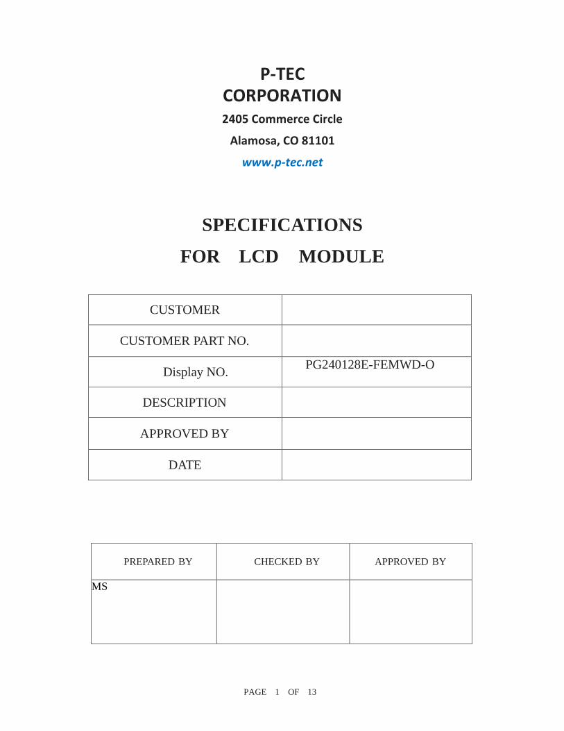
PAGE 1 OF 13
P-TEC CORPORATION 2405 Commerce Circle
Alamosa, CO 81101
www.p-tec.net
SPECIFICATIONS
FOR LCD MODULE
CUSTOMER
CUSTOMER PART NO.
Display NO. PG240128E-FEMWD-O
DESCRIPTION
APPROVED BY
DATE
PREPARED BY
CHECKED BY
APPROVED BY
MS

PAGE 2 OF 13
DOCUMENT REVISION HISTORY:
DATE
PAGE
DESCRIPTION
2007-04-05.
.
-
-
First release

PAGE 3 OF 13
1. Contents
2.Precautions in use of LCD Modules
3.General Specification
4.Absolute Maximum Ratings
5.Electrical Characteristics
6.Optical Characteristics
7.Interface Pin Function
8.Power Supply
9.Contour Drawing & Block Diagram
10.Timing Characteristics
11.Table of T6963C Commands
12.Quality Assurance
13.Reliability
PAGE 4 OF 13
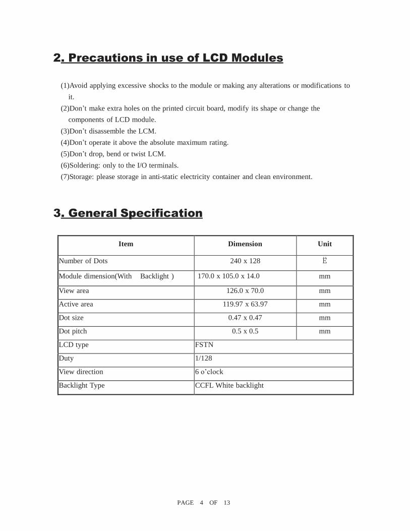
2. Precautions in use of LCD Modules
(1)Avoid applying excessive shocks to the module or making any alterations or modifications to
it.
(2)Don’t make extra holes on the printed circuit board, modify its shape or change the
components of LCD module.
(3)Don’t disassemble the LCM.
(4)Don’t operate it above the absolute maximum rating.
(5)Don’t drop, bend or twist LCM.
(6)Soldering: only to the I/O terminals.
(7)Storage: please storage in anti-static electricity container and clean environment.
3. General Specification
Item Dimension Unit
Number of Dots 240 x 128 Ё
Module dimension(With Backlight ) 170.0 x 105.0 x 14.0 mm
View area 126.0 x 70.0 mm
Active area 119.97 x 63.97 mm
Dot size 0.47 x 0.47 mm
Dot pitch 0.5 x 0.5 mm
LCD type FSTN
Duty 1/128
View direction 6 o’clock
Backlight Type CCFL White backlight

PAGE 5 OF 13
4. Absolute Maximum Ratings
Item Symbol Min Max Unit
Input Voltage VI -0.3 VDD+0.3 V
Supply Voltage For Logic VDD-VSS -0.3 7.0 V
Supply Voltage For LCD VDD-V0 Vdd-13.5 0 V
Standard
Temperature LCM
Operating Temp. Top 0 50 ć
Storage Temp. Tstr -10 60 ć
Wide Temperature
LCM
Operating Temp. Top -20 70 ć
Storage Temp. Tstr -30 80 ć
5. Electrical Characteristics
Item Symbol Condition Min Typ Max Unit
Supply Voltage For Logic VDD-VSS Ё 4.5 5.0 5.5 V
Supply Voltage For LCD VDD-V0 Ta=25ć 18.0 18.5 19.0 V
Input High Volt. VIH Ё 0.7 VDD Ё VDD V
Input Low Volt. VIL Ё VSS Ё 0.3 VDD V
Supply Current IDD VDD=5V - 47.0 53.0 mA
Supply Voltage of CCFL
backlight
VFL
current
=5 mA
252
280
306
V

PAGE 6 OF 13
6. Optical Characteristics
Item Symbol Condition Min Typ Max Unit
View Angle
(V)θ 5 -20 Ё 35 deg
(H)φ 5 -30 Ё 30 deg
Contrast Ratio CR Ё Ё 5 Ё Ё
Response Time
T rise Ё Ё Ё 250 ms
T fall Ё Ё Ё 250 ms
Definition of Operation Voltage (Vop) Definition of Response Time ( Tr , Tf )
Intensity
100ˁ
Selected Wave
Non-selected Wave
Non-selected
Conition
Intensity
Selected Conition Non-selected
Conition
Cr Max
Cr = Lon / Loff
100ˁ
90ˁ
10ˁ
Conditions :
Vop
[positive type]
Driving Voltage(V)
Tr Tf
[positive type]
Operating Voltage : Vop Viewing Angle(θΔφ) : 0°Δ 0°
Frame Frequency : 64 HZ Driving Waveform : 1/N duty , 1/a bias
Definition of viewing angle(CR 2) b
f = 180°
l r
= 270° = 90°
= 0°

PAGE 7 OF 13
7. Interface Pin Function
PIN CONNECTIONS(CN1)
PIN SYMBOL DESCRIPTION
1 FGND Frame Ground
2 GND Power Supply Ground
3 VDD Supply voltage for Logic
4 VEE Supply voltage for LCD
5 /WR Write Signal L:Active
6 /RD Read Signal L:Active
7 /CE CHIP Enable For T6963
8 C/D Data Write/Read Mode
9 NC NO Connecter
10 /RESET Reset Signal
11~18 D0-D7 Data Bus
19 FS Fonts Switch H:6*8Dots,L:8*8Dots
20 RV Display Data Reverse Signal
PIN CONNECTIONS(CN2)
1 VFL Power Supply For CFL(HOT)
2 NC NO Connecter
3 NC NO Connecter
4 NC NO Connecter
5 VFL Power Supply For CFL(GND)

PAGE 8 OF 13
8. POWER SUPPLY
Without Negative Power on PCB
With Negative Power on PCB
PAGE 9 OF 13
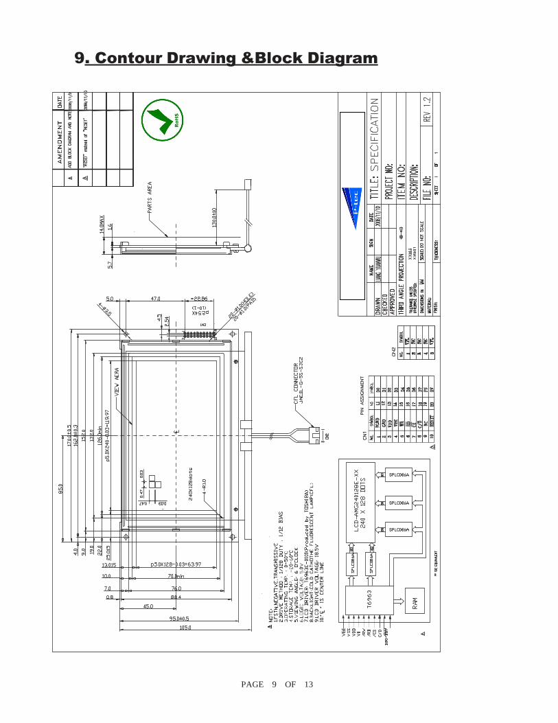
9. Contour Drawing &Block Diagram

PAGE 10 OF 13
10.Timing Characteristics
PAGE 11 OF 13
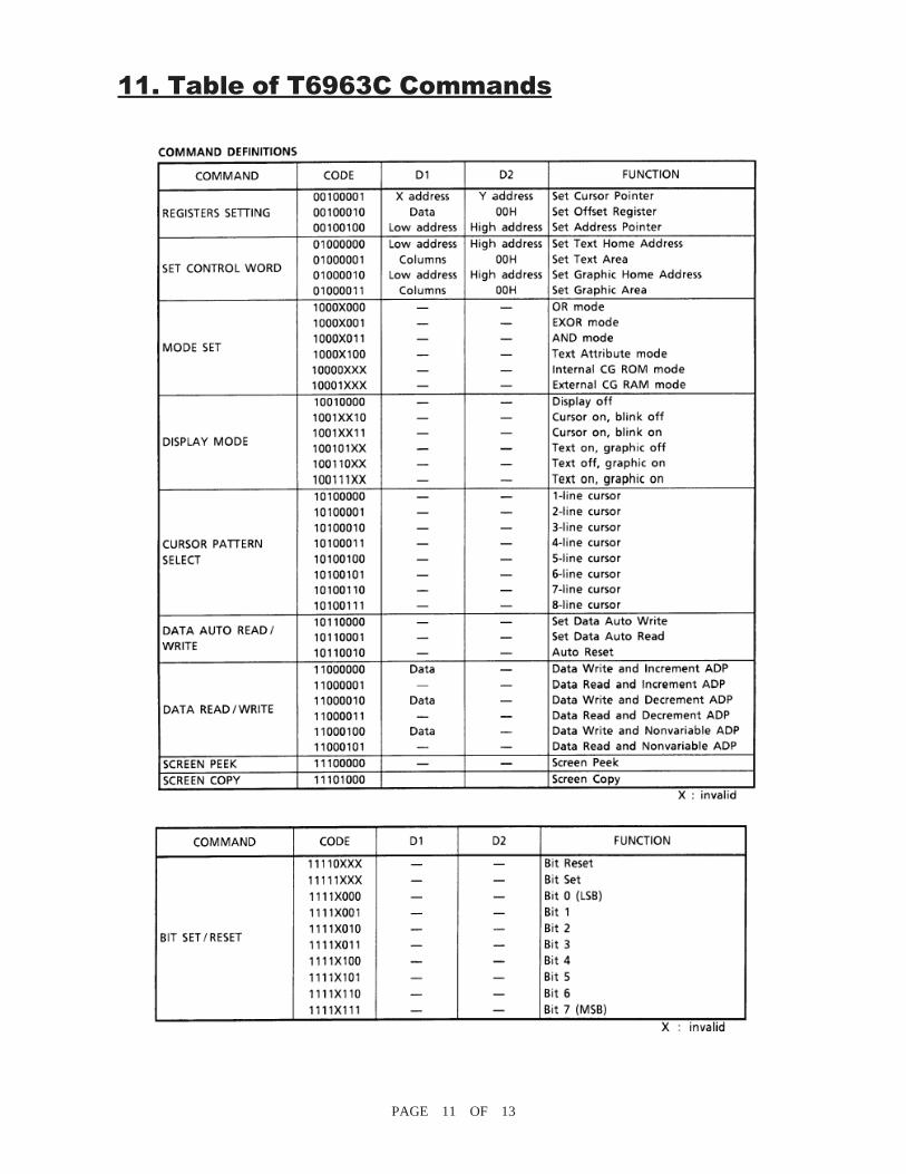
11. Table of T6963C Commands
PAGE 12 OF 13
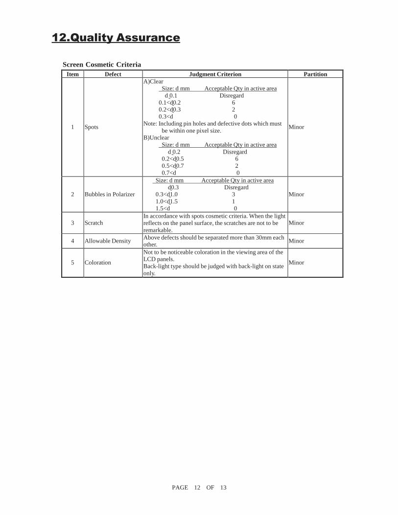
12.Quality Assurance
Screen Cosmetic Criteria
Item Defect Judgment Criterion Partition
1
Spots
A)Clear
Size: d mm Acceptable Qty in active area
d 0.1 Disregard
0.1<d 0.2 6 0.2<d 0.3 2
0.3<d 0
Note: Including pin holes and defective dots which must
be within one pixel size. B)Unclear
Size: d mm Acceptable Qty in active area
d 0.2 Disregard 0.2<d 0.5 6
0.5<d 0.7 2
0.7<d 0
Minor
2
Bubbles in Polarizer
Size: d mm Acceptable Qty in active area
d 0.3 Disregard 0.3<d 1.0 3
1.0<d 1.5 1
1.5<d 0
Minor
3
Scratch
In accordance with spots cosmetic criteria. When the light
reflects on the panel surface, the scratches are not to be
remarkable.
Minor
4
Allowable Density Above defects should be separated more than 30mm each other.
Minor
5
Coloration
Not to be noticeable coloration in the viewing area of the LCD panels.
Back-light type should be judged with back-light on state
only.
Minor
PAGE 13 OF 13
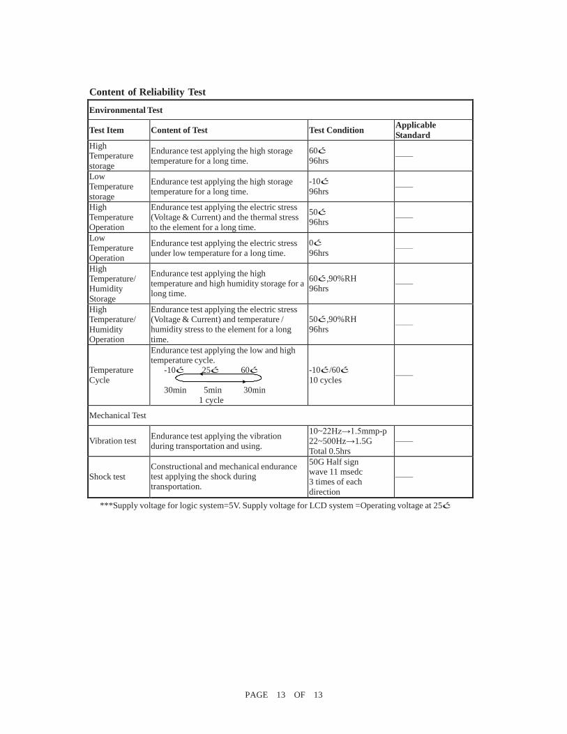
Content of Reliability Test
Environmental Test
Test Item
Content of Test
Test Condition Applicable
Standard High Temperature
storage
Endurance test applying the high storage
temperature for a long time.
60ć
96hrs
——
Low
Temperature
storage
Endurance test applying the high storage
temperature for a long time.
-10ć
96hrs
——
High
Temperature
Operation
Endurance test applying the electric stress
(Voltage & Current) and the thermal stress
to the element for a long time.
50ć
96hrs
——
Low Temperature
Operation
Endurance test applying the electric stress
under low temperature for a long time.
0ć
96hrs
——
High
Temperature/
Humidity
Storage
Endurance test applying the high
temperature and high humidity storage for a
long time.
60ć,90%RH
96hrs
——
High Temperature/
Humidity Operation
Endurance test applying the electric stress (Voltage & Current) and temperature /
humidity stress to the element for a long
time.
50ć,90%RH
96hrs
——
Temperature
Cycle
Endurance test applying the low and high temperature cycle.
-10ć 25ć 60ć
30min 5min 30min
1 cycle
-10ć/60ć
10 cycles
——
Mechanical Test
Vibration test
Endurance test applying the vibration
during transportation and using.
10~22Hz→1.5mmp-p
22~500Hz→1.5G
Total 0.5hrs
——
Shock test
Constructional and mechanical endurance test applying the shock during
transportation.
50G Half sign wave 11 msedc
3 times of each
direction
——
***Supply voltage for logic system=5V. Supply voltage for LCD system =Operating voltage at 25ć


![A arXiv:1411.1045v2 [cs.CV] 18 Dec 2014 · 2015-01-13 · Under review as a conference paper at ICLR 2015 v1 relu1 pool1 m1 v2... m5 relu5 full1... Krizhevsky/caffe network r k(x;y)](https://static.fdocuments.net/doc/165x107/5f7296fc96c262666d3d056f/a-arxiv14111045v2-cscv-18-dec-2014-2015-01-13-under-review-as-a-conference.jpg)
