PETUNJUK PEMROGRAMAN DAN SET INSTRUKSI … · Awali layanan interupsi dari sumber interupsi yang...
87
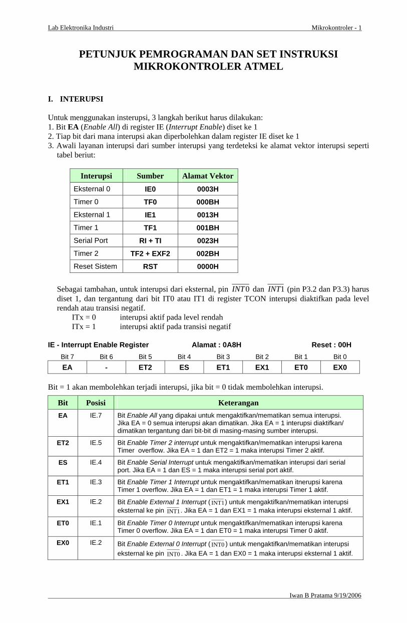
Lab Elektronika Industri Mikrokontroler - 1 PETUNJUK PEMROGRAMAN DAN SET INSTRUKSI MIKROKONTROLER ATMEL I. INTERUPSI Untuk menggunakan insterupsi, 3 langkah berikut harus dilakukan: 1. Bit EA (Enable All) di register IE (Interrupt Enable) diset ke 1 2. Tiap bit dari mana interupsi akan diperbolehkan dalam register IE diset ke 1 3. Awali layanan interupsi dari sumber interupsi yang terdeteksi ke alamat vektor interupsi seperti tabel beriut: Interupsi Sumber Alamat Vektor Eksternal 0 IE0 0003H Timer 0 TF0 000BH Eksternal 1 IE1 0013H Timer 1 TF1 001BH Serial Port RI + TI 0023H Timer 2 TF2 + EXF2 002BH Reset Sistem RST 0000H Sebagai tambahan, untuk interupsi dari eksternal, pin 0 INT dan 1 INT (pin P3.2 dan P3.3) harus diset 1, dan tergantung dari bit IT0 atau IT1 di register TCON interupsi diaktifkan pada level rendah atau transisi negatif. ITx = 0 interupsi aktif pada level rendah ITx = 1 interupsi aktif pada transisi negatif IE - Interrupt Enable Register Alamat : 0A8H Reset : 00H Bit 7 Bit 6 Bit 5 Bit 4 Bit 3 Bit 2 Bit 1 Bit 0 EA - ET2 ES ET1 EX1 ET0 EX0 Bit = 1 akan membolehkan terjadi interupsi, jika bit = 0 tidak membolehkan interupsi. Bit Posisi Keterangan EA IE.7 Bit Enable All yang dipakai untuk mengaktifkan/mematikan semua interupsi. Jika EA = 0 semua interupsi akan dimatikan. Jika EA = 1 interupsi diaktifkan/ dimatikan tergantung dari bit-bit di masing-masing sumber interupsi. ET2 IE.5 Bit Enable Timer 2 interrupt untuk mengaktifkan/mematikan interupsi karena Timer overflow. Jika EA = 1 dan ET2 = 1 maka interupsi Timer 2 aktif. ES IE.4 Bit Enable Serial Interrupt untuk mengaktifkan/mematikan interupsi dari serial port. Jika EA = 1 dan ES = 1 maka interupsi serial port aktif. ET1 IE.3 Bit Enable Timer 1 Interrupt untuk mengaktifkan/mematikan itnerupsi karena Timer 1 overflow. Jika EA = 1 dan ET1 = 1 maka interupsi Timer 1 aktif. EX1 IE.2 Bit Enable External 1 Interrupt ( INT1 ) untuk mengaktifkan/mematikan interupsi eksternal ke pin INT1 . Jika EA = 1 dan EX1 = 1 maka interupsi eksternal 1 aktif. ET0 IE.1 Bit Enable Timer 0 Interrupt untuk mengaktifkan/mematikan interupsi karena Timer 0 overflow. Jika EA = 1 dan ET0 = 1 maka interupsi Timer 0 aktif. EX0 IE.2 Bit Enable External 0 Interrupt ( INT0 ) untuk mengaktifkan/mematikan interupsi eksternal ke pin INT0 . Jika EA = 1 dan EX0 = 1 maka interupsi eksternal 1 aktif. Iwan B Pratama 9/19/2006
Transcript of PETUNJUK PEMROGRAMAN DAN SET INSTRUKSI … · Awali layanan interupsi dari sumber interupsi yang...
Lab Elektronika Industri Mikrokontroler - 1
PETUNJUK PEMROGRAMAN DAN SET INSTRUKSI MIKROKONTROLER ATMEL
I. INTERUPSI Untuk menggunakan insterupsi, 3 langkah berikut harus dilakukan: 1. Bit EA (Enable All) di register IE (Interrupt Enable) diset ke 1 2. Tiap bit dari mana interupsi akan diperbolehkan dalam register IE diset ke 1 3. Awali layanan interupsi dari sumber interupsi yang terdeteksi ke alamat vektor interupsi seperti
tabel beriut:
Interupsi Sumber Alamat Vektor Eksternal 0 IE0 0003H Timer 0 TF0 000BH Eksternal 1 IE1 0013H Timer 1 TF1 001BH Serial Port RI + TI 0023H Timer 2 TF2 + EXF2 002BH Reset Sistem RST 0000H
Sebagai tambahan, untuk interupsi dari eksternal, pin 0INT dan 1INT (pin P3.2 dan P3.3) harus diset 1, dan tergantung dari bit IT0 atau IT1 di register TCON interupsi diaktifkan pada level rendah atau transisi negatif. ITx = 0 interupsi aktif pada level rendah ITx = 1 interupsi aktif pada transisi negatif
IE - Interrupt Enable Register Alamat : 0A8H Reset : 00H
Bit 7 Bit 6 Bit 5 Bit 4 Bit 3 Bit 2 Bit 1 Bit 0 EA - ET2 ES ET1 EX1 ET0 EX0
Bit = 1 akan membolehkan terjadi interupsi, jika bit = 0 tidak membolehkan interupsi.
Bit Posisi Keterangan EA IE.7 Bit Enable All yang dipakai untuk mengaktifkan/mematikan semua interupsi.
Jika EA = 0 semua interupsi akan dimatikan. Jika EA = 1 interupsi diaktifkan/ dimatikan tergantung dari bit-bit di masing-masing sumber interupsi.
ET2 IE.5 Bit Enable Timer 2 interrupt untuk mengaktifkan/mematikan interupsi karena Timer overflow. Jika EA = 1 dan ET2 = 1 maka interupsi Timer 2 aktif.
ES IE.4 Bit Enable Serial Interrupt untuk mengaktifkan/mematikan interupsi dari serial port. Jika EA = 1 dan ES = 1 maka interupsi serial port aktif.
ET1 IE.3 Bit Enable Timer 1 Interrupt untuk mengaktifkan/mematikan itnerupsi karena Timer 1 overflow. Jika EA = 1 dan ET1 = 1 maka interupsi Timer 1 aktif.
EX1 IE.2 Bit Enable External 1 Interrupt ( INT1) untuk mengaktifkan/mematikan interupsi eksternal ke pin INT1 . Jika EA = 1 dan EX1 = 1 maka interupsi eksternal 1 aktif.
ET0 IE.1 Bit Enable Timer 0 Interrupt untuk mengaktifkan/mematikan interupsi karena Timer 0 overflow. Jika EA = 1 dan ET0 = 1 maka interupsi Timer 0 aktif.
EX0 IE.2 Bit Enable External 0 Interrupt ( INT0 ) untuk mengaktifkan/mematikan interupsi eksternal ke pin INT0 . Jika EA = 1 dan EX0 = 1 maka interupsi eksternal 1 aktif.
Iwan B Pratama 9/19/2006
Lab Elektronika Industri Mikrokontroler - 2
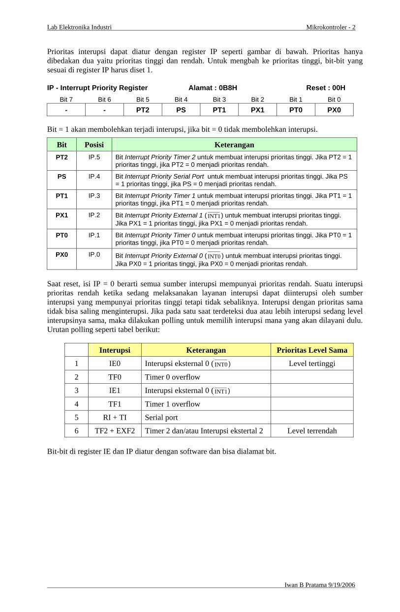
Prioritas interupsi dapat diatur dengan register IP seperti gambar di bawah. Prioritas hanya dibedakan dua yaitu prioritas tinggi dan rendah. Untuk mengbah ke prioritas tinggi, bit-bit yang sesuai di register IP harus diset 1. IP - Interrupt Priority Register Alamat : 0B8H Reset : 00H
Bit 7 Bit 6 Bit 5 Bit 4 Bit 3 Bit 2 Bit 1 Bit 0 - - PT2 PS PT1 PX1 PT0 PX0
Bit = 1 akan membolehkan terjadi interupsi, jika bit = 0 tidak membolehkan interupsi.
Bit Posisi Keterangan PT2 IP.5 Bit Interrupt Priority Timer 2 untuk membuat interupsi prioritas tinggi. Jika PT2 = 1
prioritas tinggi, jika PT2 = 0 menjadi prioritas rendah.
PS IP.4 Bit Interrupt Priority Serial Port untuk membuat interupsi prioritas tinggi. Jika PS = 1 prioritas tinggi, jika PS = 0 menjadi prioritas rendah.
PT1 IP.3 Bit Interrupt Priority Timer 1 untuk membuat interupsi prioritas tinggi. Jika PT1 = 1 prioritas tinggi, jika PT1 = 0 menjadi prioritas rendah.
PX1 IP.2 Bit Interrupt Priority External 1 ( INT1) untuk membuat interupsi prioritas tinggi. Jika PX1 = 1 prioritas tinggi, jika PX1 = 0 menjadi prioritas rendah.
PT0 IP.1 Bit Interrupt Priority Timer 0 untuk membuat interupsi prioritas tinggi. Jika PT0 = 1 prioritas tinggi, jika PT0 = 0 menjadi prioritas rendah.
PX0 IP.0 Bit Interrupt Priority External 0 ( INT0 ) untuk membuat interupsi prioritas tinggi. Jika PX0 = 1 prioritas tinggi, jika PX0 = 0 menjadi prioritas rendah.
Saat reset, isi IP = 0 berarti semua sumber interupsi mempunyai prioritas rendah. Suatu interupsi prioritas rendah ketika sedang melaksanakan layanan interupsi dapat diinterupsi oleh sumber interupsi yang mempunyai prioritas tinggi tetapi tidak sebaliknya. Interupsi dengan prioritas sama tidak bisa saling menginterupsi. Jika pada satu saat terdeteksi dua atau lebih interupsi sedang level interupsinya sama, maka dilakukan polling untuk memilih interupsi mana yang akan dilayani dulu. Urutan polling seperti tabel berikut:
Interupsi Keterangan Prioritas Level Sama
1 IE0 Interupsi eksternal 0 ( INT0 ) Level tertinggi
2 TF0 Timer 0 overflow
3 IE1 Interupsi eksternal 0 ( INT1)
4 TF1 Timer 1 overflow
5 RI + TI Serial port
6 TF2 + EXF2 Timer 2 dan/atau Interupsi ekstertal 2 Level terrendah Bit-bit di register IE dan IP diatur dengan software dan bisa dialamat bit.
Iwan B Pratama 9/19/2006
Lab Elektronika Industri Mikrokontroler - 3
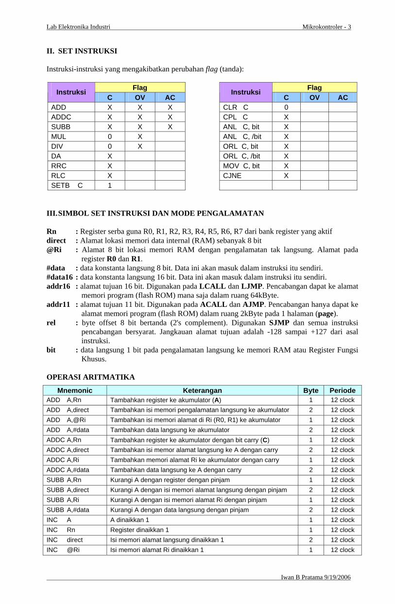
II. SET INSTRUKSI Instruksi-instruksi yang mengakibatkan perubahan flag (tanda):
Flag Flag Instruksi C OV AC
Instruksi C OV AC
ADD X X X CLR C 0 ADDC X X X CPL C X SUBB X X X ANL C, bit X MUL 0 X ANL C, /bit X DIV 0 X ORL C, bit X DA X ORL C, /bit X RRC X MOV C, bit X RLC X CJNE X SETB C 1
III. SIMBOL SET INSTRUKSI DAN MODE PENGALAMATAN Rn : Register serba guna R0, R1, R2, R3, R4, R5, R6, R7 dari bank register yang aktif direct : Alamat lokasi memori data internal (RAM) sebanyak 8 bit @Ri : Alamat 8 bit lokasi memori RAM dengan pengalamatan tak langsung. Alamat pada
register R0 dan R1. #data : data konstanta langsung 8 bit. Data ini akan masuk dalam instruksi itu sendiri. #data16 : data konstanta langsung 16 bit. Data ini akan masuk dalam instruksi itu sendiri. addr16 : alamat tujuan 16 bit. Digunakan pada LCALL dan LJMP. Pencabangan dapat ke alamat
memori program (flash ROM) mana saja dalam ruang 64kByte. addr11 : alamat tujuan 11 bit. Digunakan pada ACALL dan AJMP. Pencabangan hanya dapat ke
alamat memori program (flash ROM) dalam ruang 2kByte pada 1 halaman (page). rel : byte offset 8 bit bertanda (2's complement). Digunakan SJMP dan semua instruksi
pencabangan bersyarat. Jangkauan alamat tujuan adalah -128 sampai +127 dari asal instruksi.
bit : data langsung 1 bit pada pengalamatan langsung ke memori RAM atau Register Fungsi Khusus.
OPERASI ARITMATIKA
Mnemonic Keterangan Byte Periode ADD A,Rn Tambahkan register ke akumulator (A) 1 12 clock ADD A,direct Tambahkan isi memori pengalamatan langsung ke akumulator 2 12 clock ADD A,@Ri Tambahkan isi memori alamat di Ri (R0, R1) ke akumulator 1 12 clock ADD A,#data Tambahkan data langsung ke akumulator 2 12 clock ADDC A,Rn Tambahkan register ke akumulator dengan bit carry (C) 1 12 clock ADDC A,direct Tambahkan isi memor alamat langsung ke A dengan carry 2 12 clock ADDC A,Ri Tambahkan memori alamat Ri ke akumulator dengan carry 1 12 clock ADDC A,#data Tambahkan data langsung ke A dengan carry 2 12 clock SUBB A,Rn Kurangi A dengan register dengan pinjam 1 12 clock SUBB A,direct Kurangi A dengan isi memori alamat langsung dengan pinjam 2 12 clock SUBB A,Ri Kurangi A dengan isi memori alamat Ri dengan pinjam 1 12 clock SUBB A,#data Kurangi A dengan data langsung dengan pinjam 2 12 clock INC A A dinaikkan 1 1 12 clock INC Rn Register dinaikkan 1 1 12 clock INC direct Isi memori alamat langsung dinaikkan 1 2 12 clock INC @Ri Isi memori alamat Ri dinaikkan 1 1 12 clock
Iwan B Pratama 9/19/2006
Lab Elektronika Industri Mikrokontroler - 4
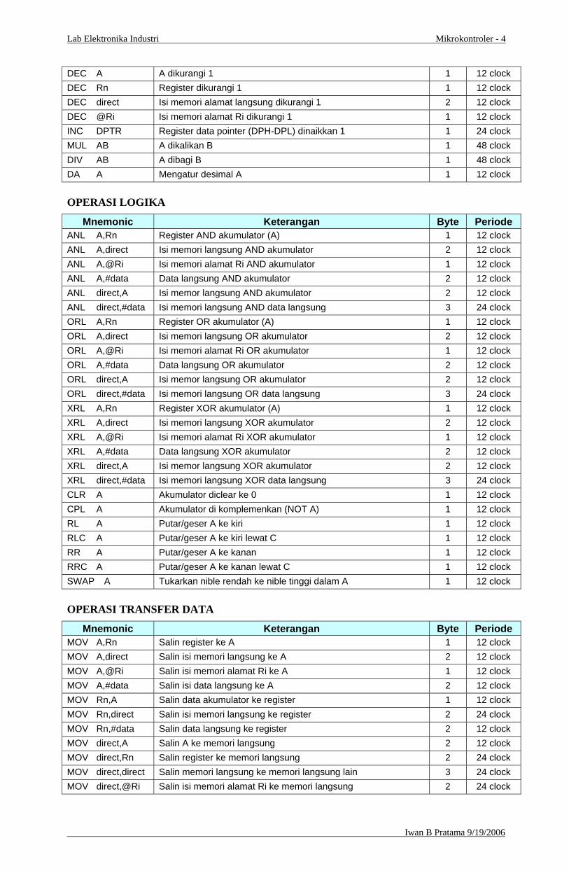
DEC A A dikurangi 1 1 12 clock DEC Rn Register dikurangi 1 1 12 clock DEC direct Isi memori alamat langsung dikurangi 1 2 12 clock DEC @Ri Isi memori alamat Ri dikurangi 1 1 12 clock INC DPTR Register data pointer (DPH-DPL) dinaikkan 1 1 24 clock MUL AB A dikalikan B 1 48 clock DIV AB A dibagi B 1 48 clock DA A Mengatur desimal A 1 12 clock OPERASI LOGIKA
Mnemonic Keterangan Byte Periode ANL A,Rn Register AND akumulator (A) 1 12 clock ANL A,direct Isi memori langsung AND akumulator 2 12 clock ANL A,@Ri Isi memori alamat Ri AND akumulator 1 12 clock ANL A,#data Data langsung AND akumulator 2 12 clock ANL direct,A Isi memor langsung AND akumulator 2 12 clock ANL direct,#data Isi memori langsung AND data langsung 3 24 clock ORL A,Rn Register OR akumulator (A) 1 12 clock ORL A,direct Isi memori langsung OR akumulator 2 12 clock ORL A,@Ri Isi memori alamat Ri OR akumulator 1 12 clock ORL A,#data Data langsung OR akumulator 2 12 clock ORL direct,A Isi memor langsung OR akumulator 2 12 clock ORL direct,#data Isi memori langsung OR data langsung 3 24 clock XRL A,Rn Register XOR akumulator (A) 1 12 clock XRL A,direct Isi memori langsung XOR akumulator 2 12 clock XRL A,@Ri Isi memori alamat Ri XOR akumulator 1 12 clock XRL A,#data Data langsung XOR akumulator 2 12 clock XRL direct,A Isi memor langsung XOR akumulator 2 12 clock XRL direct,#data Isi memori langsung XOR data langsung 3 24 clock CLR A Akumulator diclear ke 0 1 12 clock CPL A Akumulator di komplemenkan (NOT A) 1 12 clock RL A Putar/geser A ke kiri 1 12 clock RLC A Putar/geser A ke kiri lewat C 1 12 clock RR A Putar/geser A ke kanan 1 12 clock RRC A Putar/geser A ke kanan lewat C 1 12 clock SWAP A Tukarkan nible rendah ke nible tinggi dalam A 1 12 clock OPERASI TRANSFER DATA
Mnemonic Keterangan Byte Periode MOV A,Rn Salin register ke A 1 12 clock MOV A,direct Salin isi memori langsung ke A 2 12 clock MOV A,@Ri Salin isi memori alamat Ri ke A 1 12 clock MOV A,#data Salin isi data langsung ke A 2 12 clock MOV Rn,A Salin data akumulator ke register 1 12 clock MOV Rn,direct Salin isi memori langsung ke register 2 24 clock MOV Rn,#data Salin data langsung ke register 2 12 clock MOV direct,A Salin A ke memori langsung 2 12 clock MOV direct,Rn Salin register ke memori langsung 2 24 clock MOV direct,direct Salin memori langsung ke memori langsung lain 3 24 clock MOV direct,@Ri Salin isi memori alamat Ri ke memori langsung 2 24 clock
Iwan B Pratama 9/19/2006
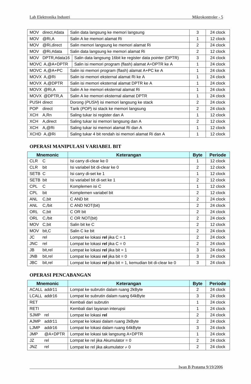
Lab Elektronika Industri Mikrokontroler - 5
MOV direct,#data Salin data langsung ke memori langsung 3 24 clock MOV @Ri,A Salin A ke memori alamat Ri 1 12 clock MOV @Ri,direct Salin memori langsung ke memori alamat Ri 2 24 clock MOV @Ri,#data Salin data langsung ke memori alamat Ri 2 12 clock MOV DPTR,#data16 Salin data langsung 16bit ke register data pointer (DPTR) 3 24 clock MOVC A,@A+DPTR Salin isi memori program (flash) alamat A+DPTR ke A 1 24 clock MOVC A,@A+PC Salin isi memori program (flash) alamat A+PC ke A 1 24 clock MOVX A,@Ri Salin isi memori eksternal alamat Ri ke A 1 24 clock MOVX A,@DPTR Salin isi memori eksternal alamat DPTR ke A 1 24 clock MOVX @Ri,A Salin A ke memori eksternal alamat Ri 1 24 clock MOVX @DPTR,A Salin A ke memori eksternal alamat DPTR 1 24 clock PUSH direct Dorong (PUSH) isi memori langsung ke stack 2 24 clock POP direct Tarik (POP) isi stack ke memori langsung 2 24 clock XCH A,Rn Saling tukar isi register dan A 1 12 clock XCH A,direct Saling tukar isi memori langsung dan A 2 12 clock XCH A,@Ri Saling tukar isi memori alamat Ri dan A 1 12 clock XCHD A,@Ri Saling tukar 4 bit rendah isi memori alamat Ri dan A 1 12 clock OPERASI MANIPULASI VARIABEL BIT
Mnemonic Keterangan Byte Periode CLR C Isi carry di-clear ke 0 1 12 clock CLR bit Isi variabel bit di-clear ke 0 2 12 clock SETB C Isi carry di-set ke 1 1 12 clock SETB bit Isi variabel bit di-set ke 1 2 12 clock CPL C Komplemen isi C 1 12 clock CPL bit Komplemen variabel bit 2 12 clock ANL C,bit C AND bit 2 24 clock ANL C,/bit C AND NOT(bit) 2 24 clock ORL C,bit C OR bit 2 24 clock ORL C,/bit C OR NOT(bit) 2 24 clock MOV C,bit Salin bit ke C 2 12 clock MOV bit,C Salin C ke bit 2 24 clock JC rel Lompat ke lokasi rel jika C = 1 2 24 clock JNC rel Lompat ke lokasi rel jika C = 0 2 24 clock JB bit,rel Lompat ke lokasi rel jika bit = 1 3 24 clock JNB bit,rel Lompat ke lokasi rel jika bit = 0 3 24 clock JBC bit,rel Lompat ke lokasi rel jika bit = 1, kemudian bit di-clear ke 0 3 24 clock OPERASI PENCABANGAN
Mnemonic Keterangan Byte Periode ACALL addr11 Lompat ke subrutin dalam ruang 2kByte 2 24 clock LCALL addr16 Lompat ke subrutin dalam ruang 64kByte 3 24 clock RET Kembali dari subrutin 1 24 clock RETI Kembali dari layanan interupsi 1 24 clock SJMP rel Lompat ke lokasi rel 2 24 clock AJMP addr11 Lompat ke lokasi dalam ruang 2kByte 2 24 clock LJMP addr16 Lompat ke lokasi dalam ruang 64kByte 3 24 clock JMP @A+DPTR Lompat ke lokasi tak langsung A+DPTR 1 24 clock JZ rel Lompat ke rel jika Akumulator = 0 2 24 clock JNZ rel Lompat ke rel jika akumulator ≠ 0 2 24 clock
Iwan B Pratama 9/19/2006
Lab Elektronika Industri Mikrokontroler - 6
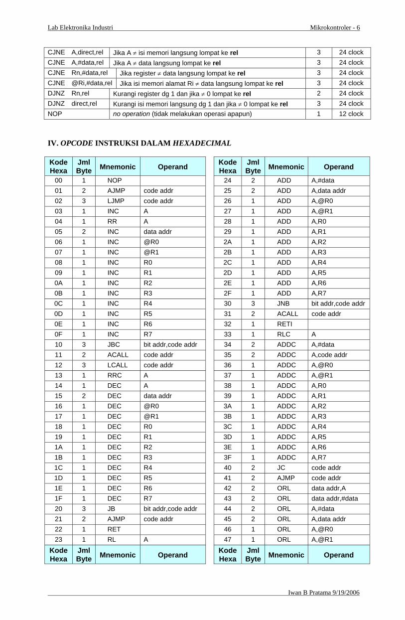
CJNE A,direct,rel Jika A ≠ isi memori langsung lompat ke rel 3 24 clock CJNE A,#data,rel Jika A ≠ data langsung lompat ke rel 3 24 clock CJNE Rn,#data,rel Jika register ≠ data langsung lompat ke rel 3 24 clock CJNE @Ri,#data,rel Jika isi memori alamat Ri ≠ data langsung lompat ke rel 3 24 clock DJNZ Rn,rel Kurangi register dg 1 dan jika ≠ 0 lompat ke rel 2 24 clock DJNZ direct,rel Kurangi isi memori langsung dg 1 dan jika ≠ 0 lompat ke rel 3 24 clock NOP no operation (tidak melakukan operasi apapun) 1 12 clock IV. OPCODE INSTRUKSI DALAM HEXADECIMAL Kode Hexa
Jml Byte Mnemonic Operand Kode
Hexa Jml Byte Mnemonic Operand
00 1 NOP 24 2 ADD A,#data 01 2 AJMP code addr 25 2 ADD A,data addr 02 3 LJMP code addr 26 1 ADD A,@R0 03 1 INC A 27 1 ADD A,@R1 04 1 RR A 28 1 ADD A,R0 05 2 INC data addr 29 1 ADD A,R1 06 1 INC @R0 2A 1 ADD A,R2 07 1 INC @R1 2B 1 ADD A,R3 08 1 INC R0 2C 1 ADD A,R4 09 1 INC R1 2D 1 ADD A,R5 0A 1 INC R2 2E 1 ADD A,R6 0B 1 INC R3 2F 1 ADD A,R7 0C 1 INC R4 30 3 JNB bit addr,code addr 0D 1 INC R5 31 2 ACALL code addr 0E 1 INC R6 32 1 RETI 0F 1 INC R7 33 1 RLC A 10 3 JBC bit addr,code addr 34 2 ADDC A,#data 11 2 ACALL code addr 35 2 ADDC A,code addr 12 3 LCALL code addr 36 1 ADDC A,@R0 13 1 RRC A 37 1 ADDC A,@R1 14 1 DEC A 38 1 ADDC A,R0 15 2 DEC data addr 39 1 ADDC A,R1 16 1 DEC @R0 3A 1 ADDC A,R2 17 1 DEC @R1 3B 1 ADDC A,R3 18 1 DEC R0 3C 1 ADDC A,R4 19 1 DEC R1 3D 1 ADDC A,R5 1A 1 DEC R2 3E 1 ADDC A,R6 1B 1 DEC R3 3F 1 ADDC A,R7 1C 1 DEC R4 40 2 JC code addr 1D 1 DEC R5 41 2 AJMP code addr 1E 1 DEC R6 42 2 ORL data addr,A 1F 1 DEC R7 43 2 ORL data addr,#data 20 3 JB bit addr,code addr 44 2 ORL A,#data 21 2 AJMP code addr 45 2 ORL A,data addr 22 1 RET 46 1 ORL A,@R0 23 1 RL A 47 1 ORL A,@R1
Kode Hexa
Jml Byte Mnemonic Operand Kode
Hexa Jml Byte Mnemonic Operand
Iwan B Pratama 9/19/2006
Lab Elektronika Industri Mikrokontroler - 7
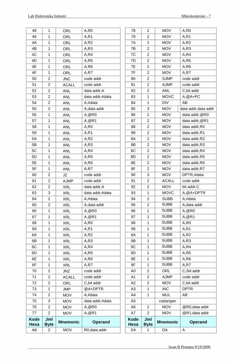
48 1 ORL A,R0 78 2 MOV A,R0 49 1 ORL A,R1 79 2 MOV A,R1 4A 1 ORL A,R2 7A 2 MOV A,R2 4B 1 ORL A,R3 7B 2 MOV A,R3 4C 1 ORL A,R4 7C 2 MOV A,R4 4D 1 ORL A,R5 7D 2 MOV A,R5 4E 1 ORL A,R6 7E 2 MOV A,R6 4F 1 ORL A,R7 7F 2 MOV A,R7 50 2 JNC code addr 80 2 SJMP code addr 51 2 ACALL code addr 81 2 AJMP code addr 52 2 ANL data addr,A 82 2 ANL C,bit addr 53 2 ANL data addr,#data 83 1 MOVC A,@A+PC 54 2 ANL A,#data 84 1 DIV AB 55 2 ANL A,data addr 85 3 MOV data addr,data addr 56 1 ANL A,@R0 86 2 MOV data addr,@R0 57 1 ANL A,@R1 87 2 MOV data addr,@R1 58 1 ANL A,R0 88 2 MOV data addr,R0 59 1 ANL A,R1 89 2 MOV data addr,R1 5A 1 ANL A,R2 8A 2 MOV data addr,R2 5B 1 ANL A,R3 8B 2 MOV data addr,R3 5C 1 ANL A,R4 8C 2 MOV data addr,R4 5D 1 ANL A,R5 8D 2 MOV data addr,R5 5E 1 ANL A,R6 8E 2 MOV data addr,R6 5F 1 ANL A,R7 8F 2 MOV data addr,R7 60 2 JZ code addr 90 3 MOV DPTR,#data 61 2 AJMP code addr 91 2 ACALL code addr 62 2 XRL data addr,A 92 2 MOV bit addr,C 63 3 XRL data addr,#data 93 1 MOVC A,@A+DPTR 64 2 XRL A,#data 94 2 SUBB A,#data 65 2 XRL A,data addr 95 2 SUBB A,data addr 66 1 XRL A,@R0 96 1 SUBB A,@R0 67 1 XRL A,@R1 97 1 SUBB A,@R1 68 1 XRL A,R0 98 1 SUBB A,R0 69 1 XRL A,R1 99 1 SUBB A,R1 6A 1 XRL A,R2 9A 1 SUBB A,R2 6B 1 XRL A,R3 9B 1 SUBB A,R3 6C 1 XRL A,R4 9C 1 SUBB A,R4 6D 1 XRL A,R5 9D 1 SUBB A,R5 6E 1 XRL A,R6 9E 1 SUBB A,R6 6F 1 XRL A,R7 9F 1 SUBB A,R7 70 2 JNZ code addr A0 2 ORL C,/bit addr 71 2 ACALL code addr A1 2 AJMP code addr 72 2 ORL C,bit addr A2 2 MOV C,bit addr 73 1 JMP @A+DPTR A3 1 INC DPTR 74 2 MOV A,#data A4 1 MUL AB 75 3 MOV data addr,#data A5 cadangan 76 2 MOV A,@R0 A6 2 MOV @R0,data addr 77 2 MOV A,@R1 A7 2 MOV @R1,data addr
Kode Hexa
Jml Byte Mnemonic Operand Kode
Hexa Jml Byte Mnemonic Operand
A8 2 MOV R0,data addr D4 1 DA A
Iwan B Pratama 9/19/2006
Lab Elektronika Industri Mikrokontroler - 8
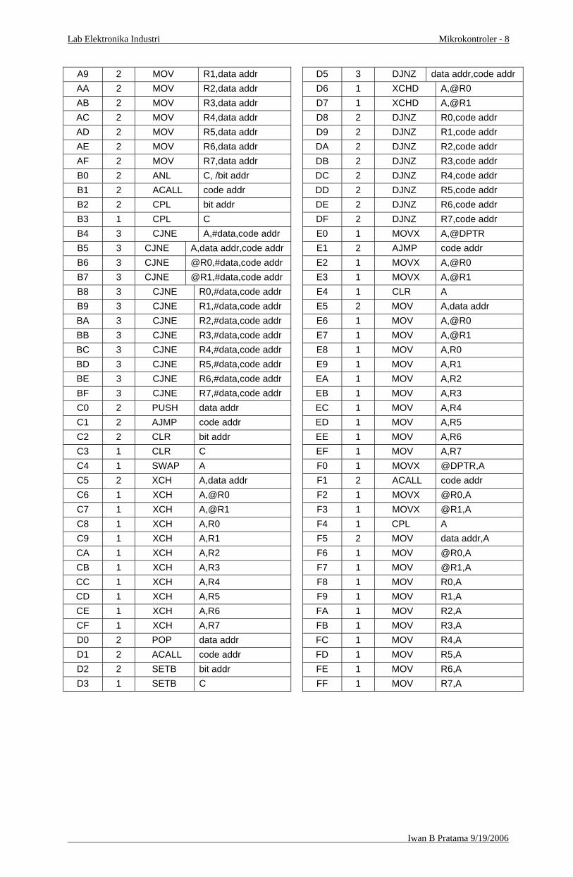
A9 2 MOV R1,data addr D5 3 DJNZ data addr,code addr AA 2 MOV R2,data addr D6 1 XCHD A,@R0 AB 2 MOV R3,data addr D7 1 XCHD A,@R1 AC 2 MOV R4,data addr D8 2 DJNZ R0,code addr AD 2 MOV R5,data addr D9 2 DJNZ R1,code addr AE 2 MOV R6,data addr DA 2 DJNZ R2,code addr AF 2 MOV R7,data addr DB 2 DJNZ R3,code addr B0 2 ANL C, /bit addr DC 2 DJNZ R4,code addr B1 2 ACALL code addr DD 2 DJNZ R5,code addr B2 2 CPL bit addr DE 2 DJNZ R6,code addr B3 1 CPL C DF 2 DJNZ R7,code addr B4 3 CJNE A,#data,code addr E0 1 MOVX A,@DPTR B5 3 CJNE A,data addr,code addr E1 2 AJMP code addr B6 3 CJNE @R0,#data,code addr E2 1 MOVX A,@R0 B7 3 CJNE @R1,#data,code addr E3 1 MOVX A,@R1 B8 3 CJNE R0,#data,code addr E4 1 CLR A B9 3 CJNE R1,#data,code addr E5 2 MOV A,data addr BA 3 CJNE R2,#data,code addr E6 1 MOV A,@R0 BB 3 CJNE R3,#data,code addr E7 1 MOV A,@R1 BC 3 CJNE R4,#data,code addr E8 1 MOV A,R0 BD 3 CJNE R5,#data,code addr E9 1 MOV A,R1 BE 3 CJNE R6,#data,code addr EA 1 MOV A,R2 BF 3 CJNE R7,#data,code addr EB 1 MOV A,R3 C0 2 PUSH data addr EC 1 MOV A,R4 C1 2 AJMP code addr ED 1 MOV A,R5 C2 2 CLR bit addr EE 1 MOV A,R6 C3 1 CLR C EF 1 MOV A,R7 C4 1 SWAP A F0 1 MOVX @DPTR,A C5 2 XCH A,data addr F1 2 ACALL code addr C6 1 XCH A,@R0 F2 1 MOVX @R0,A C7 1 XCH A,@R1 F3 1 MOVX @R1,A C8 1 XCH A,R0 F4 1 CPL A C9 1 XCH A,R1 F5 2 MOV data addr,A CA 1 XCH A,R2 F6 1 MOV @R0,A CB 1 XCH A,R3 F7 1 MOV @R1,A CC 1 XCH A,R4 F8 1 MOV R0,A CD 1 XCH A,R5 F9 1 MOV R1,A CE 1 XCH A,R6 FA 1 MOV R2,A CF 1 XCH A,R7 FB 1 MOV R3,A D0 2 POP data addr FC 1 MOV R4,A D1 2 ACALL code addr FD 1 MOV R5,A D2 2 SETB bit addr FE 1 MOV R6,A D3 1 SETB C FF 1 MOV R7,A
Iwan B Pratama 9/19/2006

Instruction Set
Notes on Data Addressing Modes
Rn - Working register R0-R7
direct - 128 internal RAM locations, any l/O port, control or status register
@Ri - Indirect internal or external RAM location addressed by register R0 or R1
#data - 8-bit constant included in instruction
#data 16 - 16-bit constant included as bytes 2 and 3 of instruction
bit - 128 software flags, any bitaddressable l/O pin, control or status bit
Semiconductor Group 1
A - Accumulator
Notes on Program Addressing Modes
addr16 - Destination address for LCALL and LJMP may be anywhere within the 64-Kbyte program memory address space.
addr11 - Destination address for ACALL and AJMP will be within the same 2-Kbyte page of program memory as the first byte of the following instruction.
rel - SJMP and all conditional jumps include an 8 bit offset byte. Range is + 127/– 128 bytes relative to the first byte of the following instruction.
All mnemonics copyrighted: Intel Corporation 1980
Instruction Set
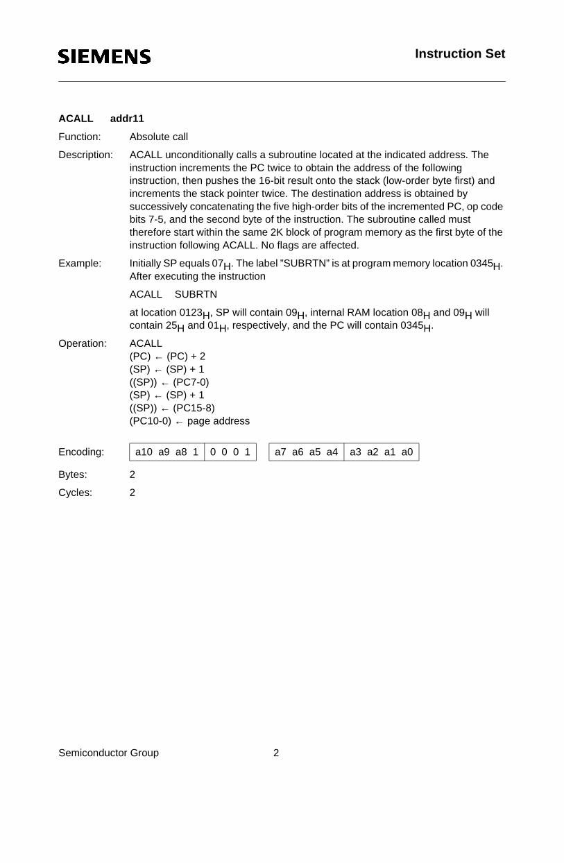
ACALL addr11
Function: Absolute call
Description: ACALL unconditionally calls a subroutine located at the indicated address. The instruction increments the PC twice to obtain the address of the following instruction, then pushes the 16-bit result onto the stack (low-order byte first) and increments the stack pointer twice. The destination address is obtained by successively concatenating the five high-order bits of the incremented PC, op code bits 7-5, and the second byte of the instruction. The subroutine called must therefore start within the same 2K block of program memory as the first byte of the
Semiconductor Group 2
instruction following ACALL. No flags are affected.
Example: Initially SP equals 07H. The label ”SUBRTN” is at program memory location 0345H. After executing the instruction
ACALL SUBRTN
at location 0123H, SP will contain 09H, internal RAM location 08H and 09H will contain 25H and 01H, respectively, and the PC will contain 0345H.
Operation: ACALL(PC) ← (PC) + 2(SP) ← (SP) + 1((SP)) ← (PC7-0)(SP) ← (SP) + 1((SP)) ← (PC15-8)(PC10-0) ← page address
Bytes: 2
Cycles: 2
Encoding: a10 a9 a8 1 0 0 0 1 a7 a6 a5 a4 a3 a2 a1 a0
Instruction Set
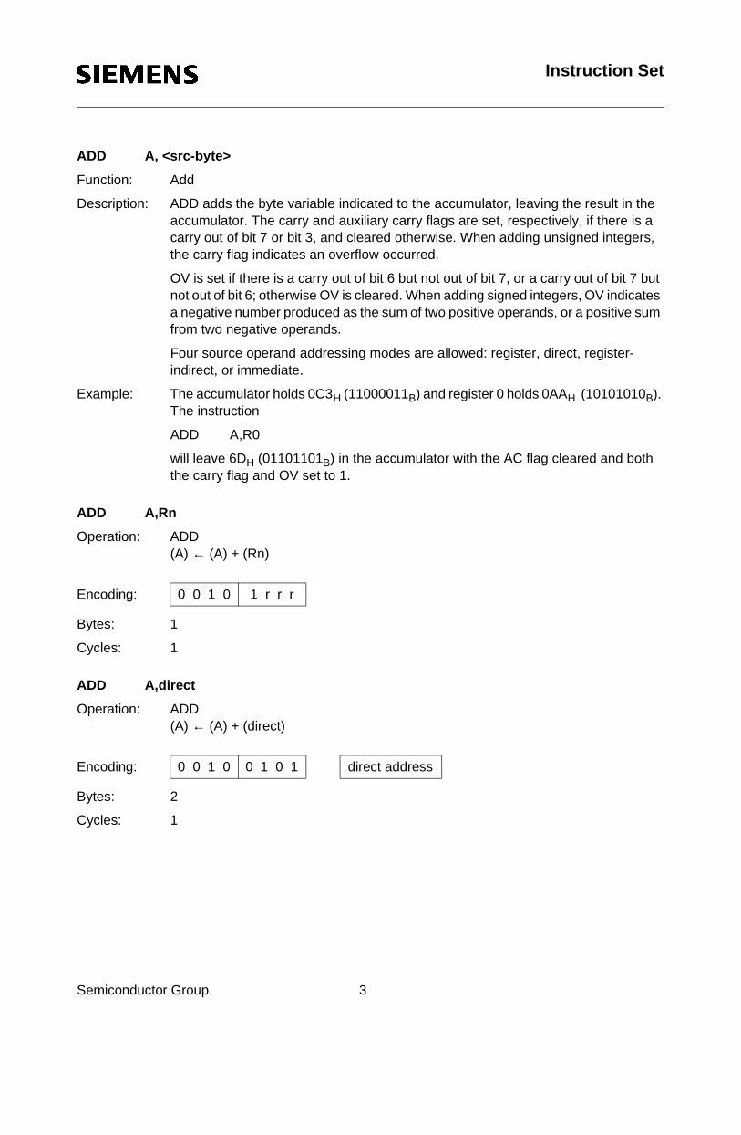
ADD A, <src-byte>
Function: Add
Description: ADD adds the byte variable indicated to the accumulator, leaving the result in the accumulator. The carry and auxiliary carry flags are set, respectively, if there is a carry out of bit 7 or bit 3, and cleared otherwise. When adding unsigned integers, the carry flag indicates an overflow occurred.
OV is set if there is a carry out of bit 6 but not out of bit 7, or a carry out of bit 7 but not out of bit 6; otherwise OV is cleared. When adding signed integers, OV indicates a negative number produced as the sum of two positive operands, or a positive sum
Semiconductor Group 3
from two negative operands.
Four source operand addressing modes are allowed: register, direct, register-indirect, or immediate.
Example: The accumulator holds 0C3H (11000011B) and register 0 holds 0AAH (10101010B). The instruction
ADD A,R0
will leave 6DH (01101101B) in the accumulator with the AC flag cleared and both the carry flag and OV set to 1.
ADD A,Rn
Operation: ADD(A) ← (A) + (Rn)
Bytes: 1
Cycles: 1
ADD A,direct
Operation: ADD(A) ← (A) + (direct)
Bytes: 2
Cycles: 1
Encoding: 0 0 1 0 1 r r r
Encoding: 0 0 1 0 0 1 0 1 direct address

Instruction Set
ADD A, @Ri
Operation: ADD(A) ← (A) + ((Ri))
Bytes: 1
Cycles: 1
Encoding: 0 0 1 0 0 1 1 i
Semiconductor Group 4
ADD A, #data
Operation: ADD(A) ← (A) + #data
Bytes: 2
Cycles: 1
Encoding: 0 0 1 0 0 1 0 0 immediate data
Instruction Set
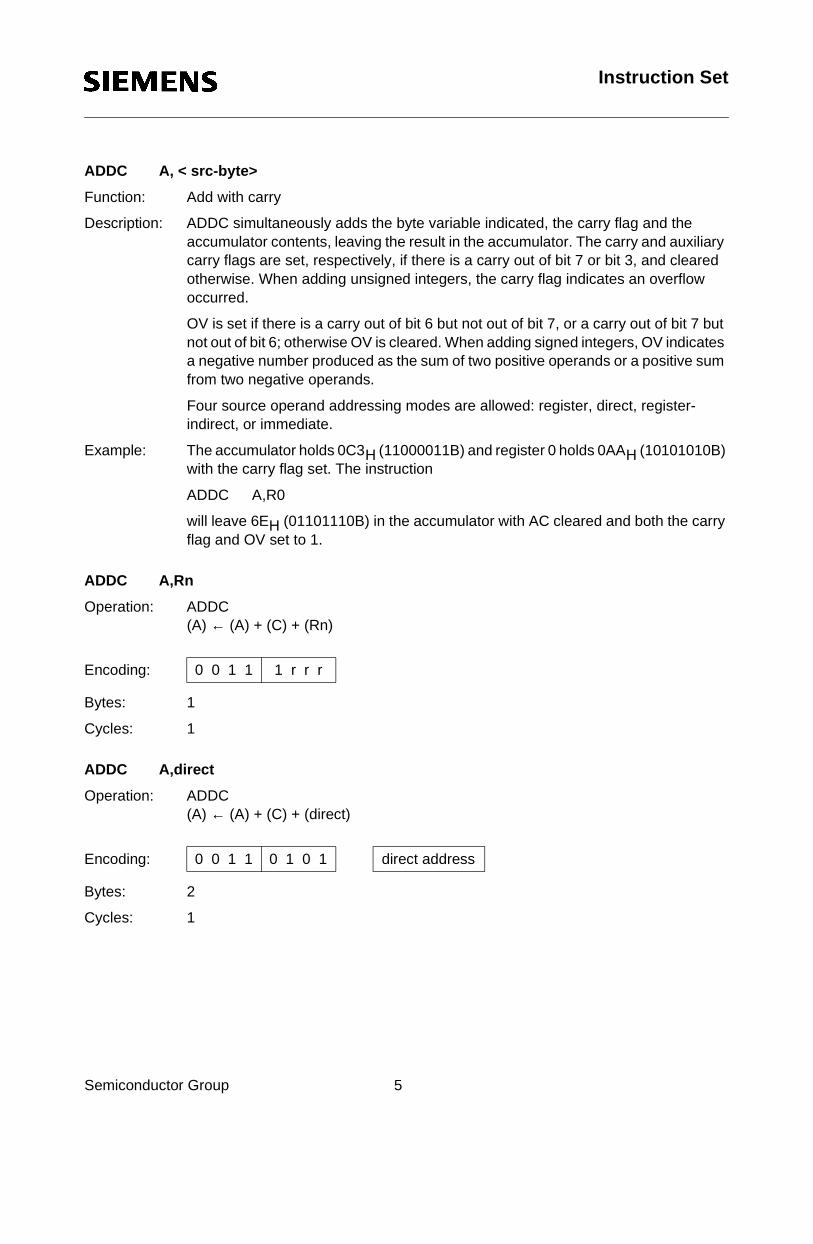
ADDC A, < src-byte>
Function: Add with carry
Description: ADDC simultaneously adds the byte variable indicated, the carry flag and the accumulator contents, leaving the result in the accumulator. The carry and auxiliary carry flags are set, respectively, if there is a carry out of bit 7 or bit 3, and cleared otherwise. When adding unsigned integers, the carry flag indicates an overflow occurred.
OV is set if there is a carry out of bit 6 but not out of bit 7, or a carry out of bit 7 but not out of bit 6; otherwise OV is cleared. When adding signed integers, OV indicates
Semiconductor Group 5
a negative number produced as the sum of two positive operands or a positive sum from two negative operands.
Four source operand addressing modes are allowed: register, direct, register-indirect, or immediate.
Example: The accumulator holds 0C3H (11000011B) and register 0 holds 0AAH (10101010B) with the carry flag set. The instruction
ADDC A,R0
will leave 6EH (01101110B) in the accumulator with AC cleared and both the carry flag and OV set to 1.
ADDC A,Rn
Operation: ADDC(A) ← (A) + (C) + (Rn)
Bytes: 1
Cycles: 1
ADDC A,direct
Operation: ADDC(A) ← (A) + (C) + (direct)
Bytes: 2
Cycles: 1
Encoding: 0 0 1 1 1 r r r
Encoding: 0 0 1 1 0 1 0 1 direct address
Instruction Set
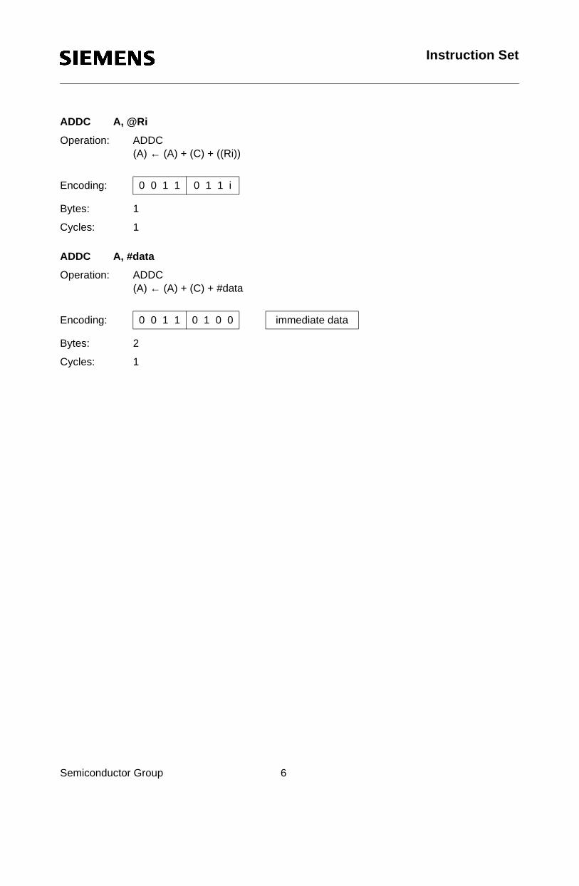
ADDC A, @Ri
Operation: ADDC(A) ← (A) + (C) + ((Ri))
Bytes: 1
Cycles: 1
Encoding: 0 0 1 1 0 1 1 i
Semiconductor Group 6
ADDC A, #data
Operation: ADDC(A) ← (A) + (C) + #data
Bytes: 2
Cycles: 1
Encoding: 0 0 1 1 0 1 0 0 immediate data
Instruction Set
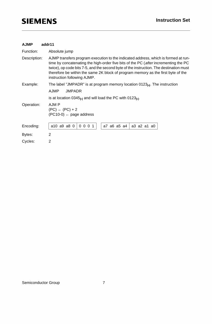
AJMP addr11
Function: Absolute jump
Description: AJMP transfers program execution to the indicated address, which is formed at run-time by concatenating the high-order five bits of the PC (after incrementing the PC twice), op code bits 7-5, and the second byte of the instruction. The destination must therefore be within the same 2K block of program memory as the first byte of the instruction following AJMP.
Example: The label ”JMPADR” is at program memory location 0123H. The instruction
AJMP JMPADR
Semiconductor Group 7
is at location 0345H and will load the PC with 0123H.
Operation: AJM P(PC) ← (PC) + 2(PC10-0) ← page address
Bytes: 2
Cycles: 2
Encoding: a10 a9 a8 0 0 0 0 1 a7 a6 a5 a4 a3 a2 a1 a0

Instruction Set
ANL <dest-byte>, <src-byte>
Function: Logical AND for byte variables
Description: ANL performs the bitwise logical AND operation between the variables indicated and stores the results in the destination variable. No flags are affected.
The two operands allow six addressing mode combinations. When the destination is a accumulator, the source can use register, direct, register-indirect, or immediate addressing; when the destination is a direct address, the source can be the accumulator or immediate data.
Semiconductor Group 8
Note:
When this instruction is used to modify an output port, the value used as the original port data will be read from the output data latch, not the input pins.
Example: If the accumulator holds 0C3H (11000011B) and register 0 holds 0AAH (10101010B) then the instruction
ANL A,R0
will leave 81H (10000001B) in the accumulator.
When the destination is a directly addressed byte, this instruction will clear combinations of bits in any RAM location or hardware register. The mask byte determining the pattern of bits to be cleared would either be a constant contained in the instruction or a value computed in the accumulator at run-time.The instruction
ANL P1, #01110011B
will clear bits 7, 3, and 2 of output port 1.
ANL A,Rn
Operation: ANL(A) ← (A) ∧ (Rn)
Bytes: 1
Cycles: 1
Encoding: 0 1 0 1 1 r r r

Instruction Set
ANL A,direct
Operation: ANL(A) ← (A) ∧ (direct)
Bytes: 2
Cycles: 1
Encoding: 0 1 0 1 0 1 0 1 direct address
Semiconductor Group 9
ANL A, @Ri
Operation: ANL(A) ← (A) ∧ ((Ri))
Bytes: 1
Cycles: 1
ANL A, #data
Operation: ANL(A) ← (A) ∧ #data
Bytes: 2
Cycles: 1
ANL direct,A
Operation: ANL(direct) ← (direct) ∧ (A)
Bytes: 2
Cycles: 1
Encoding: 0 1 0 1 0 1 1 i
Encoding: 0 1 0 1 0 1 0 0 immediate data
Encoding: 0 1 0 1 0 1 0 1 direct address

Instruction Set
ANL direct, #data
Operation: ANL(direct) ← (direct) ∧ #data
Bytes: 3
Cycles: 2
Encoding: 0 1 0 1 0 0 1 1 direct address immediate data
Semiconductor Group 10
Instruction Set
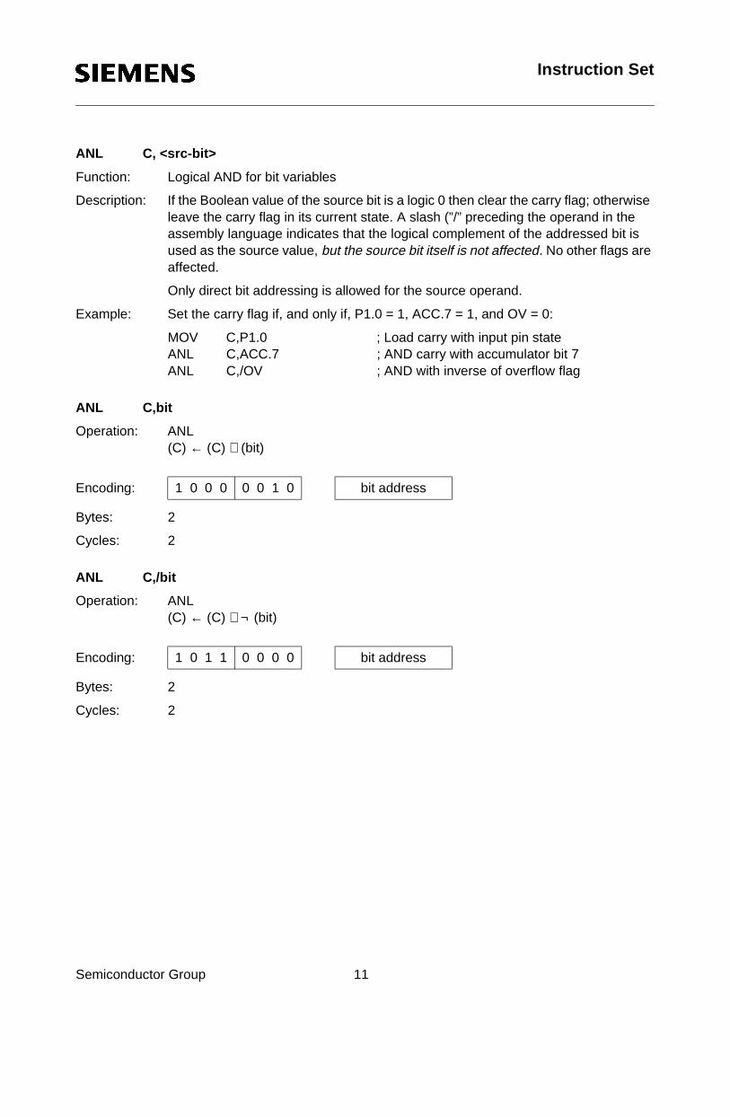
ANL C, <src-bit>
Function: Logical AND for bit variables
Description: If the Boolean value of the source bit is a logic 0 then clear the carry flag; otherwise leave the carry flag in its current state. A slash (”/” preceding the operand in the assembly language indicates that the logical complement of the addressed bit is used as the source value, but the source bit itself is not affected. No other flags are affected.
Only direct bit addressing is allowed for the source operand.
Example: Set the carry flag if, and only if, P1.0 = 1, ACC.7 = 1, and OV = 0:
Semiconductor Group 11
MOV C,P1.0 ; Load carry with input pin stateANL C,ACC.7 ; AND carry with accumulator bit 7ANL C,/OV ; AND with inverse of overflow flag
ANL C,bit
Operation: ANL(C) ← (C) ∧ (bit)
Bytes: 2
Cycles: 2
ANL C,/bit
Operation: ANL(C) ← (C) ∧ ¬ (bit)
Bytes: 2
Cycles: 2
Encoding: 1 0 0 0 0 0 1 0 bit address
Encoding: 1 0 1 1 0 0 0 0 bit address
Instruction Set
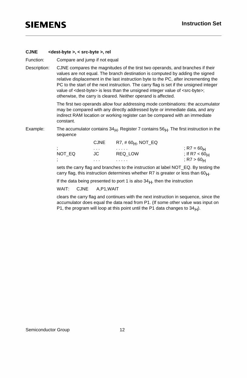
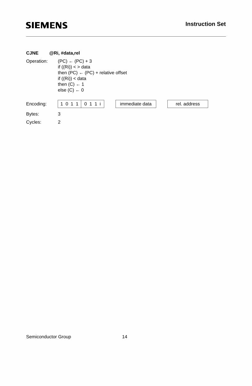
CJNE <dest-byte >, < src-byte >, rel
Function: Compare and jump if not equal
Description: CJNE compares the magnitudes of the tirst two operands, and branches if their values are not equal. The branch destination is computed by adding the signed relative displacement in the last instruction byte to the PC, after incrementing the PC to the start of the next instruction. The carry flag is set if the unsigned integer value of <dest-byte> is less than the unsigned integer value of <src-byte>; otherwise, the carry is cleared. Neither operand is affected.
The first two operands allow four addressing mode combinations: the accumulator
Semiconductor Group 12
may be compared with any directly addressed byte or immediate data, and any indirect RAM location or working register can be compared with an immediate constant.
Example: The accumulator contains 34H. Register 7 contains 56H. The first instruction in the sequence
CJNE R7, # 60H, NOT_EQ; . . . . . . . . ; R7 = 60HNOT_EQ JC REQ_LOW ; If R7 < 60H; . . . . . . . . ; R7 > 60H
sets the carry flag and branches to the instruction at label NOT_EQ. By testing the carry flag, this instruction determines whether R7 is greater or less than 60H.
If the data being presented to port 1 is also 34H, then the instruction
WAIT: CJNE A,P1,WAIT
clears the carry flag and continues with the next instruction in sequence, since the accumulator does equal the data read from P1. (If some other value was input on P1, the program will loop at this point until the P1 data changes to 34H).
Instruction Set
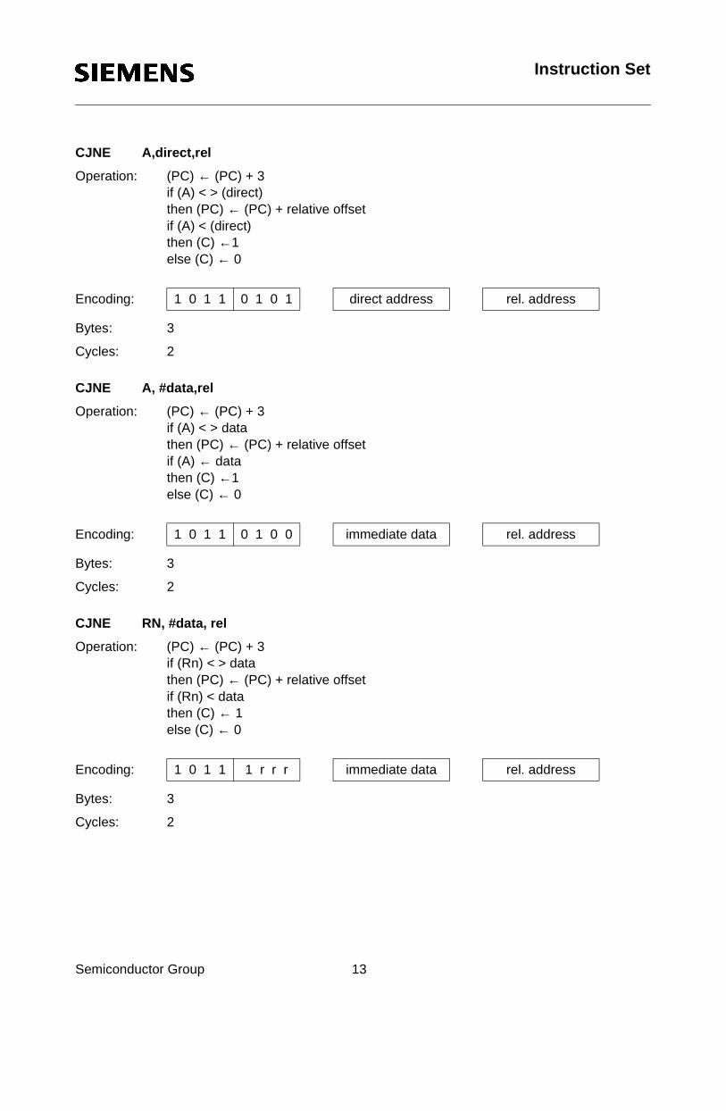
CJNE A,direct,rel
Operation: (PC) ← (PC) + 3if (A) < > (direct)then (PC) ← (PC) + relative offsetif (A) < (direct)then (C) ←1else (C) ← 0
Encoding: 1 0 1 1 0 1 0 1 direct address rel. address
Semiconductor Group 13
Bytes: 3
Cycles: 2
CJNE A, #data,rel
Operation: (PC) ← (PC) + 3if (A) < > datathen (PC) ← (PC) + relative offsetif (A) ← datathen (C) ←1else (C) ← 0
Bytes: 3
Cycles: 2
CJNE RN, #data, rel
Operation: (PC) ← (PC) + 3if (Rn) < > datathen (PC) ← (PC) + relative offsetif (Rn) < datathen (C) ← 1else (C) ← 0
Bytes: 3
Cycles: 2
Encoding: 1 0 1 1 0 1 0 0 immediate data rel. address
Encoding: 1 0 1 1 1 r r r immediate data rel. address
Instruction Set
CJNE @Ri, #data,rel
Operation: (PC) ← (PC) + 3if ((Ri)) < > datathen (PC) ← (PC) + relative offsetif ((Ri)) < datathen (C) ← 1else (C) ← 0
Encoding: 1 0 1 1 0 1 1 i immediate data rel. address
Semiconductor Group 14
Bytes: 3
Cycles: 2
Instruction Set
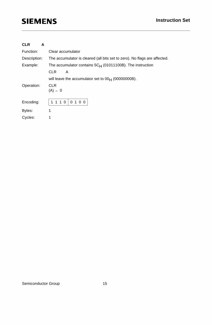
CLR A
Function: Clear accumulator
Description: The accumulator is cleared (all bits set to zero). No flags are affected.
Example: The accumulator contains 5CH (01011100B). The instruction
CLR A
will leave the accumulator set to 00H (00000000B).
Operation: CLR(A) ← 0
Semiconductor Group 15
Bytes: 1
Cycles: 1
Encoding: 1 1 1 0 0 1 0 0
Instruction Set
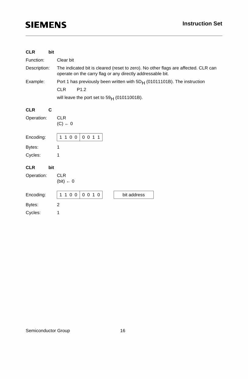
CLR bit
Function: Clear bit
Description: The indicated bit is cleared (reset to zero). No other flags are affected. CLR can operate on the carry flag or any directly addressable bit.
Example: Port 1 has previously been written with 5DH (01011101B). The instruction
CLR P1.2
will leave the port set to 59H (01011001B).
Semiconductor Group 16
CLR C
Operation: CLR(C) ← 0
Bytes: 1
Cycles: 1
CLR bit
Operation: CLR(bit) ← 0
Bytes: 2
Cycles: 1
Encoding: 1 1 0 0 0 0 1 1
Encoding: 1 1 0 0 0 0 1 0 bit address
Instruction Set
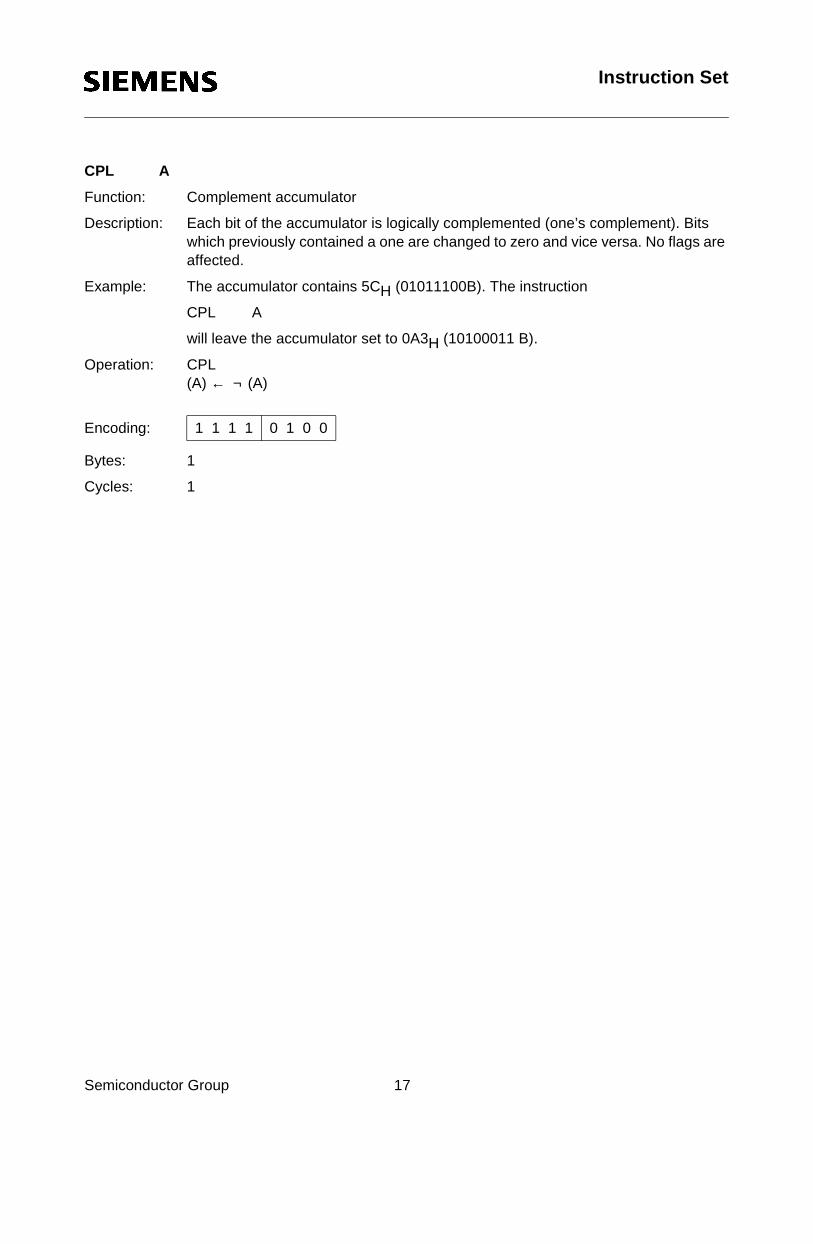
CPL A
Function: Complement accumulator
Description: Each bit of the accumulator is logically complemented (one’s complement). Bits which previously contained a one are changed to zero and vice versa. No flags are affected.
Example: The accumulator contains 5CH (01011100B). The instruction
CPL A
will leave the accumulator set to 0A3H (10100011 B).
Semiconductor Group 17
Operation: CPL(A) ← ¬ (A)
Bytes: 1
Cycles: 1
Encoding: 1 1 1 1 0 1 0 0
Instruction Set
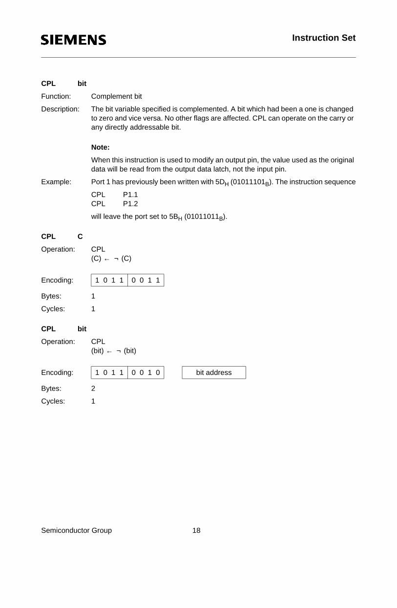
CPL bit
Function: Complement bit
Description: The bit variable specified is complemented. A bit which had been a one is changed to zero and vice versa. No other flags are affected. CPL can operate on the carry or any directly addressable bit.
Note:
When this instruction is used to modify an output pin, the value used as the original data will be read from the output data latch, not the input pin.
Semiconductor Group 18
Example: Port 1 has previously been written with 5DH (01011101B). The instruction sequence
CPL P1.1 CPL P1.2
will leave the port set to 5BH (01011011B).
CPL C
Operation: CPL(C) ← ¬ (C)
Bytes: 1
Cycles: 1
CPL bit
Operation: CPL(bit) ← ¬ (bit)
Bytes: 2
Cycles: 1
Encoding: 1 0 1 1 0 0 1 1
Encoding: 1 0 1 1 0 0 1 0 bit address
Instruction Set
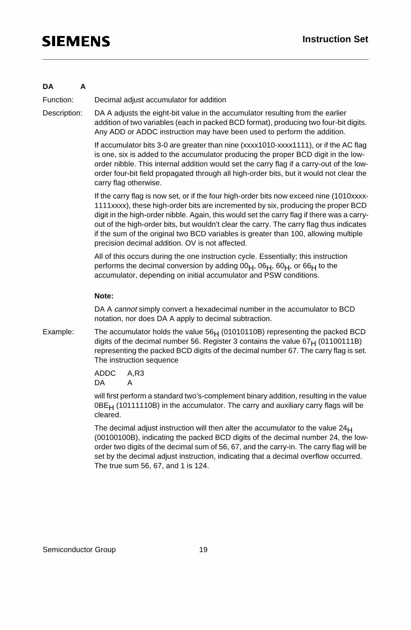
DA A
Function: Decimal adjust accumulator for addition
Description: DA A adjusts the eight-bit value in the accumulator resulting from the earlier addition of two variables (each in packed BCD format), producing two four-bit digits. Any ADD or ADDC instruction may have been used to perform the addition.
If accumulator bits 3-0 are greater than nine (xxxx1010-xxxx1111), or if the AC flag is one, six is added to the accumulator producing the proper BCD digit in the low-order nibble. This internal addition would set the carry flag if a carry-out of the low-order four-bit field propagated through all high-order bits, but it would not clear the
Semiconductor Group 19
carry flag otherwise.
If the carry flag is now set, or if the four high-order bits now exceed nine (1010xxxx-1111xxxx), these high-order bits are incremented by six, producing the proper BCD digit in the high-order nibble. Again, this would set the carry flag if there was a carry-out of the high-order bits, but wouldn’t clear the carry. The carry flag thus indicates if the sum of the original two BCD variables is greater than 100, allowing multiple precision decimal addition. OV is not affected.
All of this occurs during the one instruction cycle. Essentially; this instruction performs the decimal conversion by adding 00H, 06H, 60H, or 66H to the accumulator, depending on initial accumulator and PSW conditions.
Note:
DA A cannot simply convert a hexadecimal number in the accumulator to BCD notation, nor does DA A apply to decimal subtraction.
Example: The accumulator holds the value 56H (01010110B) representing the packed BCD digits of the decimal number 56. Register 3 contains the value 67H (01100111B) representing the packed BCD digits of the decimal number 67. The carry flag is set. The instruction sequence
ADDC A,R3DA A
will first perform a standard two’s-complement binary addition, resulting in the value 0BEH (10111110B) in the accumulator. The carry and auxiliary carry flags will be cleared.
The decimal adjust instruction will then alter the accumulator to the value 24H (00100100B), indicating the packed BCD digits of the decimal number 24, the low-order two digits of the decimal sum of 56, 67, and the carry-in. The carry flag will be set by the decimal adjust instruction, indicating that a decimal overflow occurred. The true sum 56, 67, and 1 is 124.
Instruction Set
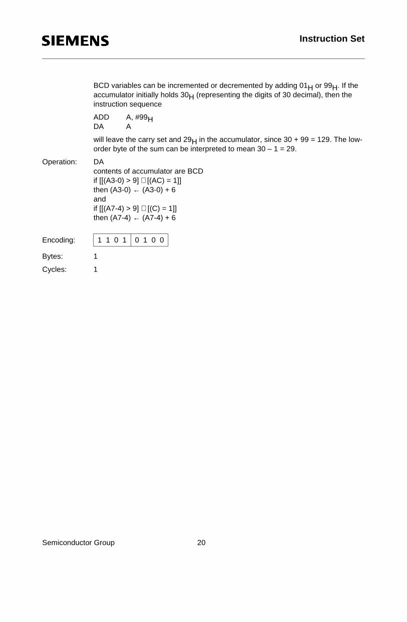
BCD variables can be incremented or decremented by adding 01H or 99H. If the accumulator initially holds 30H (representing the digits of 30 decimal), then the instruction sequence
ADD A, #99HDA A
will leave the carry set and 29H in the accumulator, since 30 + 99 = 129. The low-order byte of the sum can be interpreted to mean 30 – 1 = 29.
Operation: DAcontents of accumulator are BCD
Semiconductor Group 20
if [[(A3-0) > 9] ∨ [(AC) = 1]]then (A3-0) ← (A3-0) + 6andif [[(A7-4) > 9] ∨ [(C) = 1]]then (A7-4) ← (A7-4) + 6
Bytes: 1
Cycles: 1
Encoding: 1 1 0 1 0 1 0 0
Instruction Set
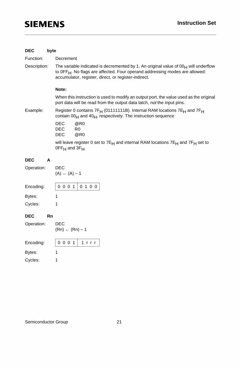
DEC byte
Function: Decrement
Description: The variable indicated is decremented by 1. An original value of 00H will underflow to 0FFH. No flags are affected. Four operand addressing modes are allowed: accumulator, register, direct, or register-indirect.
Note:
When this instruction is used to modify an output port, the value used as the original port data will be read from the output data latch, not the input pins.
Semiconductor Group 21
Example: Register 0 contains 7FH (01111111B). Internal RAM locations 7EH and 7FH contain 00H and 40H, respectively. The instruction sequence
DEC @R0DEC R0DEC @R0
will leave register 0 set to 7EH and internal RAM locations 7EH and 7FH set to 0FFH and 3FH.
DEC A
Operation: DEC(A) ← (A) – 1
Bytes: 1
Cycles: 1
DEC Rn
Operation: DEC(Rn) ← (Rn) – 1
Bytes: 1
Cycles: 1
Encoding: 0 0 0 1 0 1 0 0
Encoding: 0 0 0 1 1 r r r
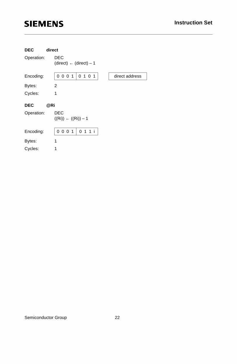
Instruction Set
DEC direct
Operation: DEC(direct) ← (direct) – 1
Bytes: 2
Cycles: 1
Encoding: 0 0 0 1 0 1 0 1 direct address
Semiconductor Group 22
DEC @Ri
Operation: DEC((Ri)) ← ((Ri)) – 1
Bytes: 1
Cycles: 1
Encoding: 0 0 0 1 0 1 1 i
Instruction SetInstruction Set
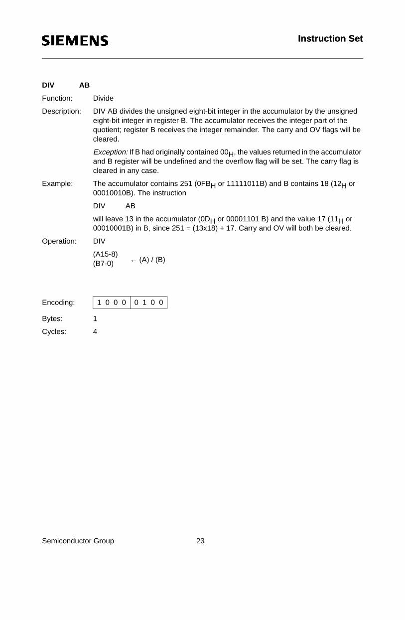
DIV AB
Function: Divide
Description: DIV AB divides the unsigned eight-bit integer in the accumulator by the unsigned eight-bit integer in register B. The accumulator receives the integer part of the quotient; register B receives the integer remainder. The carry and OV flags will be cleared.
Exception: If B had originally contained 00H, the values returned in the accumulator and B register will be undefined and the overflow flag will be set. The carry flag is cleared in any case.
Semiconductor Group 23
Example: The accumulator contains 251 (0FBH or 11111011B) and B contains 18 (12H or 00010010B). The instruction
DIV AB
will leave 13 in the accumulator (0DH or 00001101 B) and the value 17 (11H or 00010001B) in B, since 251 = (13x18) + 17. Carry and OV will both be cleared.
Operation: DIV
(A15-8)(B7-0)
Bytes: 1
Cycles: 4
Encoding: 1 0 0 0 0 1 0 0
← (A) / (B)
Instruction Set
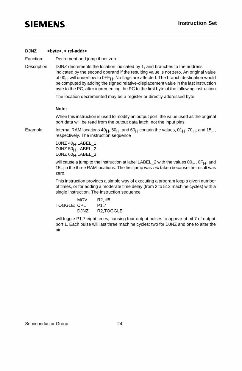
DJNZ <byte>, < rel-addr>
Function: Decrement and jump if not zero
Description: DJNZ decrements the location indicated by 1, and branches to the address indicated by the second operand if the resulting value is not zero. An original value of 00H will underflow to 0FFH. No flags are affected. The branch destination would be computed by adding the signed relative-displacement value in the last instruction byte to the PC, after incrementing the PC to the first byte of the following instruction.
The location decremented may be a register or directly addressed byte.
Semiconductor Group 24
Note:
When this instruction is used to modify an output port, the value used as the original port data will be read from the output data latch, not the input pins.
Example: Internal RAM locations 40H, 50H, and 60H contain the values, 01H, 70H, and 15H, respectively. The instruction sequence
DJNZ 40H,LABEL_1DJNZ 50H,LABEL_2DJNZ 60H,LABEL_3
will cause a jump to the instruction at label LABEL_2 with the values 00H, 6FH, and 15H in the three RAM locations. The first jump was not taken because the result was zero.
This instruction provides a simple way of executing a program loop a given number of times, or for adding a moderate time delay (from 2 to 512 machine cycles) with a single instruction. The instruction sequence
MOV R2, #8TOGGLE: CPL P1.7
DJNZ R2,TOGGLE
will toggle P1.7 eight times, causing four output pulses to appear at bit 7 of output port 1. Each pulse will last three machine cycles; two for DJNZ and one to alter the pin.
Instruction Set
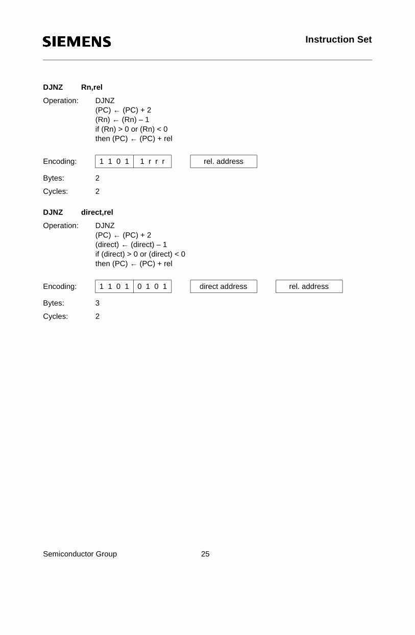
DJNZ Rn,rel
Operation: DJNZ(PC) ← (PC) + 2(Rn) ← (Rn) – 1if (Rn) > 0 or (Rn) < 0then (PC) ← (PC) + rel
Bytes: 2
Encoding: 1 1 0 1 1 r r r rel. address
Semiconductor Group 25
Cycles: 2
DJNZ direct,rel
Operation: DJNZ(PC) ← (PC) + 2(direct) ← (direct) – 1if (direct) > 0 or (direct) < 0then (PC) ← (PC) + rel
Bytes: 3
Cycles: 2
Encoding: 1 1 0 1 0 1 0 1 direct address rel. address
Instruction Set
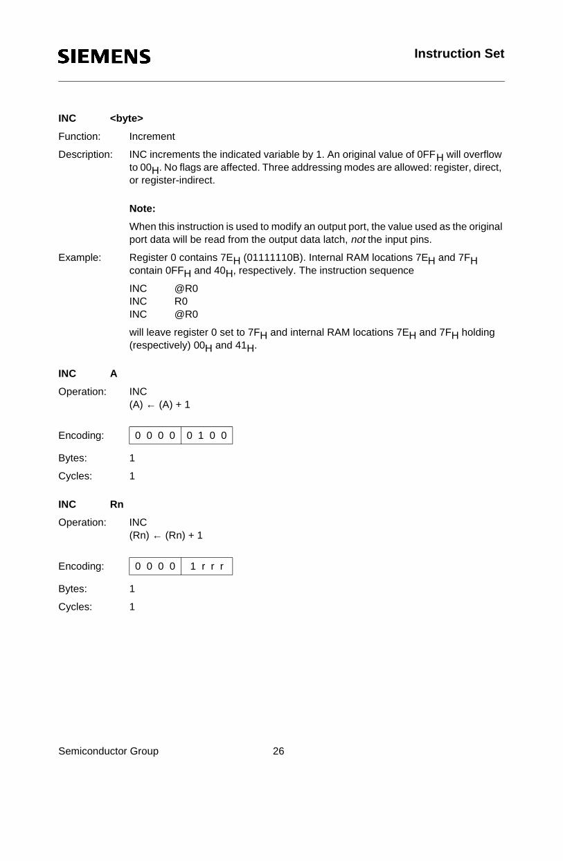
INC <byte>
Function: Increment
Description: INC increments the indicated variable by 1. An original value of 0FFH will overflow to 00H. No flags are affected. Three addressing modes are allowed: register, direct, or register-indirect.
Note:
When this instruction is used to modify an output port, the value used as the original port data will be read from the output data latch, not the input pins.
Semiconductor Group 26
Example: Register 0 contains 7EH (01111110B). Internal RAM locations 7EH and 7FH contain 0FFH and 40H, respectively. The instruction sequence
INC @R0INC R0INC @R0
will leave register 0 set to 7FH and internal RAM locations 7EH and 7FH holding (respectively) 00H and 41H.
INC A
Operation: INC(A) ← (A) + 1
Bytes: 1
Cycles: 1
INC Rn
Operation: INC(Rn) ← (Rn) + 1
Bytes: 1
Cycles: 1
Encoding: 0 0 0 0 0 1 0 0
Encoding: 0 0 0 0 1 r r r
Instruction Set
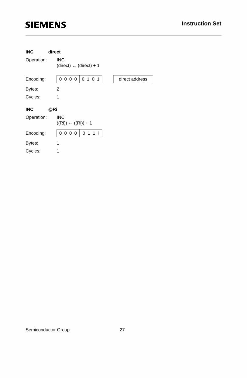
INC direct
Operation: INC(direct) ← (direct) + 1
Bytes: 2
Cycles: 1
Encoding: 0 0 0 0 0 1 0 1 direct address
Semiconductor Group 27
INC @Ri
Operation: INC((Ri)) ← ((Ri)) + 1
Bytes: 1
Cycles: 1
Encoding: 0 0 0 0 0 1 1 i
Instruction Set
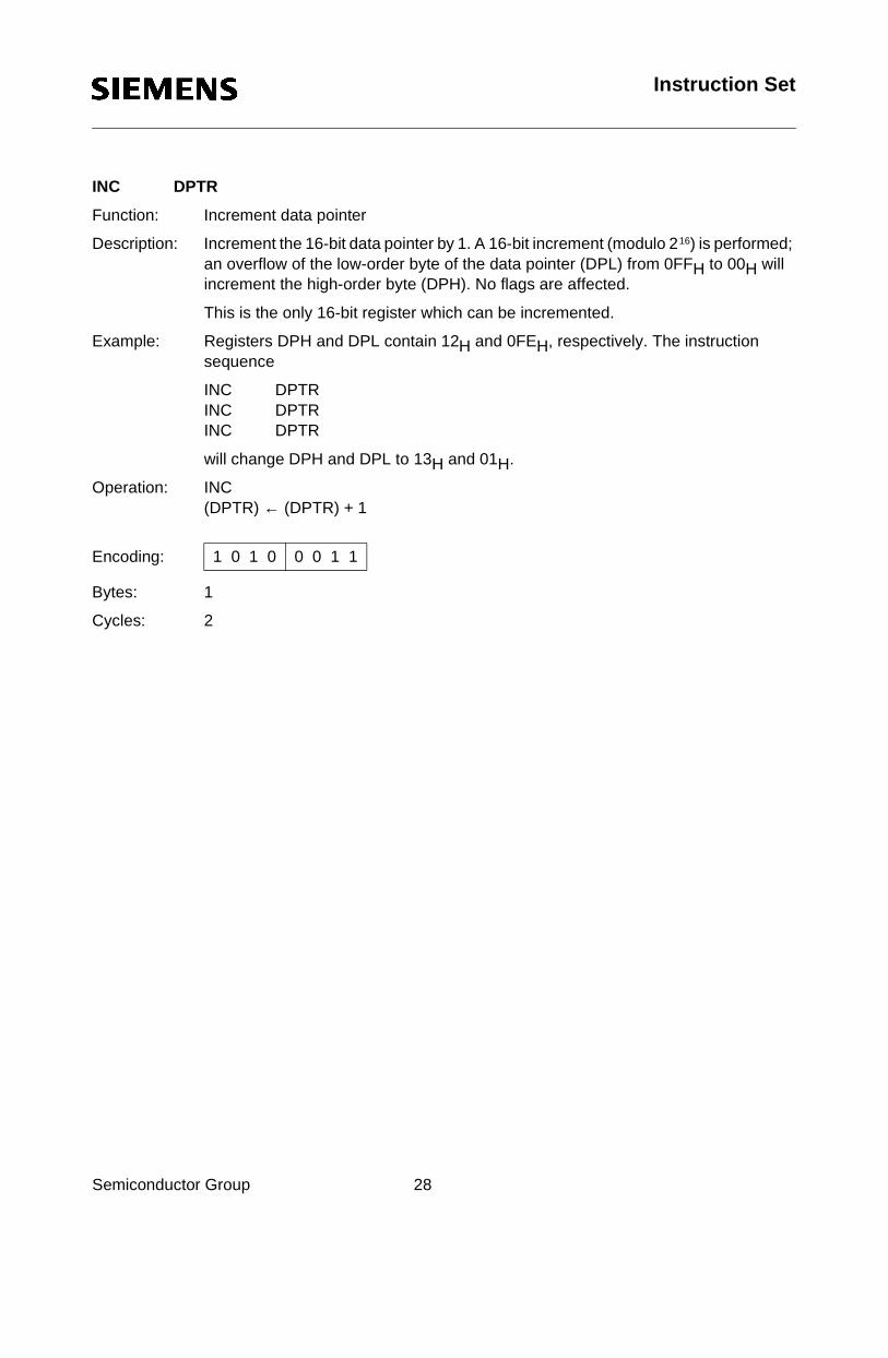
INC DPTR
Function: Increment data pointer
Description: Increment the 16-bit data pointer by 1. A 16-bit increment (modulo 216) is performed; an overflow of the low-order byte of the data pointer (DPL) from 0FFH to 00H will increment the high-order byte (DPH). No flags are affected.
This is the only 16-bit register which can be incremented.
Example: Registers DPH and DPL contain 12H and 0FEH, respectively. The instruction sequence
Semiconductor Group 28
INC DPTRINC DPTRINC DPTR
will change DPH and DPL to 13H and 01H.
Operation: INC(DPTR) ← (DPTR) + 1
Bytes: 1
Cycles: 2
Encoding: 1 0 1 0 0 0 1 1

Instruction Set
JB bit,rel
Function: Jump if bit is set
Description: If the indicated bit is a one, jump to the address indicated; otherwise proceed with the next instruction. The branch destination is computed by adding the signed relative-displacement in the third instruction byte to the PC, after incrementing the PC to the first byte of the next instruction. The bit tested is not modified. No flags are affected.
Example: The data present at input port 1 is 11001010B. The accumulator holds 56 (01010110B). The instruction sequence
Semiconductor Group 29
JB P1.2,LABEL1JB ACC.2,LABEL2
will cause program execution to branch to the instruction at label LABEL2.
Operation: JB(PC) ← (PC) + 3if (bit) = 1then (PC) ← (PC) + rel
Bytes: 3
Cycles: 2
Encoding: 0 0 1 0 0 0 0 0 bit address rel. address
Instruction Set
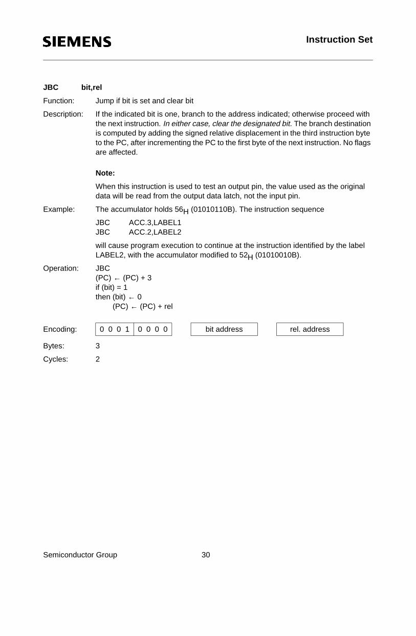
JBC bit,rel
Function: Jump if bit is set and clear bit
Description: If the indicated bit is one, branch to the address indicated; otherwise proceed with the next instruction. In either case, clear the designated bit. The branch destination is computed by adding the signed relative displacement in the third instruction byte to the PC, after incrementing the PC to the first byte of the next instruction. No flags are affected.
Note:
Semiconductor Group 30
When this instruction is used to test an output pin, the value used as the original data will be read from the output data latch, not the input pin.
Example: The accumulator holds 56H (01010110B). The instruction sequence
JBC ACC.3,LABEL1JBC ACC.2,LABEL2
will cause program execution to continue at the instruction identified by the label LABEL2, with the accumulator modified to 52H (01010010B).
Operation: JBC(PC) ← (PC) + 3if (bit) = 1then (bit) ← 0 (PC) ← (PC) + rel
Bytes: 3
Cycles: 2
Encoding: 0 0 0 1 0 0 0 0 bit address rel. address
Instruction Set
JC rel
Function: Jump if carry is set
Description: If the carry flag is set, branch to the address indicated; otherwise proceed with the next instruction. The branch destination is computed by adding the signed relative-displacement in the second instruction byte to the PC, after incrementing the PC twice. No flags are affected.
Example: The carry flag is cleared. The instruction sequence
JC LABEL1CPL C
Semiconductor Group 31
JC LABEL2
will set the carry and cause program execution to continue at the instruction identified by the label LABEL2.
Operation: JC(PC) ← (PC) + 2if (C) = 1then (PC) ← (PC) + rel
Bytes: 2
Cycles: 2
Encoding: 0 1 0 0 0 0 0 0 rel. address
Instruction Set
JMP @A + DPTR
Function: Jump indirect
Description: Add the eight-bit unsigned contents of the accumulator with the sixteen-bit data pointer, and load the resulting sum to the program counter. This will be the address for subsequent instruction fetches. Sixteen-bit addition is performed (modulo 216): a carry-out from the low-order eight bits propagates through the higher-order bits. Neither the accumulator nor the data pointer is altered. No flags are affected.
Example: An even number from 0 to 6 is in the accumulator. The following sequence of instructions will branch to one of four AJMP instructions in a jump table starting at
Semiconductor Group 32
JMP_TBL:
MOV DPTR, #JMP_TBLJMP @A + DPTR
JMP_TBL: AJMP LABEL0AJMP LABEL1AJMP LABEL2AJMP LABEL3
If the accumulator equals 04H when starting this sequence, execution will jump to label LABEL2. Remember that AJMP is a two-byte instruction, so the jump instructions start at every other address.
Operation: JMP(PC) ← (A) + (DPTR)
Bytes: 1
Cycles: 2
Encoding: 0 1 1 1 0 0 1 1
Instruction Set
JNB bit,rel
Function: Jump if bit is not set
Description: If the indicated bit is a zero, branch to the indicated address; otherwise proceed with the next instruction. The branch destination is computed by adding the signed relative-displacement in the third instruction byte to the PC, after incrementing the PC to the first byte of the next instruction. The bit tested is not modified. No flags are affected.
Example: The data present at input port 1 is 11001010B. The accumulator holds 56H (01010110B). The instruction sequence
Semiconductor Group 33
JNB P1.3,LABEL1JNB ACC.3,LABEL2
will cause program execution to continue at the instruction at label LABEL2.
Operation: JNB(PC) ← (PC) + 3if (bit) = 0then (PC) ← (PC) + rel.
Bytes: 3
Cycles: 2
Encoding: 0 0 1 1 0 0 0 0 bit address rel. address
Instruction Set
JNC rel
Function: Jump if carry is not set
Description: If the carry flag is a zero, branch to the address indicated; otherwise proceed with the next instruction. The branch destination is computed by adding the signed relative-displacement in the second instruction byte to the PC, after incrementing the PC twice to point to the next instruction. The carry flag is not modified.
Example: The carry flag is set. The instruction sequence
JNC LABEL1CPL C
Semiconductor Group 34
JNC LABEL2
will clear the carry and cause program execution to continue at the instruction identified by the label LABEL2.
Operation: JNC(PC) ← (PC) + 2if (C) = 0then (PC) ← (PC) + rel
Bytes: 2
Cycles: 2
Encoding: 0 1 0 1 0 0 0 0 rel. address
Instruction Set
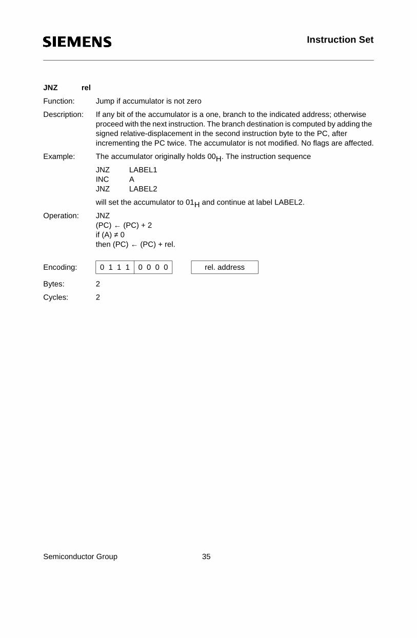
JNZ rel
Function: Jump if accumulator is not zero
Description: If any bit of the accumulator is a one, branch to the indicated address; otherwise proceed with the next instruction. The branch destination is computed by adding the signed relative-displacement in the second instruction byte to the PC, after incrementing the PC twice. The accumulator is not modified. No flags are affected.
Example: The accumulator originally holds 00H. The instruction sequence
JNZ LABEL1INC A
Semiconductor Group 35
JNZ LABEL2
will set the accumulator to 01H and continue at label LABEL2.
Operation: JNZ(PC) ← (PC) + 2if (A) ≠ 0then (PC) ← (PC) + rel.
Bytes: 2
Cycles: 2
Encoding: 0 1 1 1 0 0 0 0 rel. address
Instruction Set
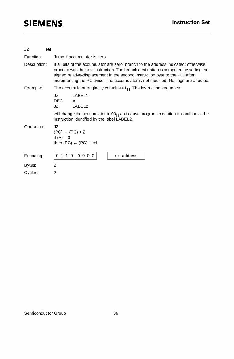
JZ rel
Function: Jump if accumulator is zero
Description: If all bits of the accumulator are zero, branch to the address indicated; otherwise proceed with the next instruction. The branch destination is computed by adding the signed relative-displacement in the second instruction byte to the PC, after incrementing the PC twice. The accumulator is not modified. No flags are affected.
Example: The accumulator originally contains 01H. The instruction sequence
JZ LABEL1DEC A
Semiconductor Group 36
JZ LABEL2
will change the accumulator to 00H and cause program execution to continue at the instruction identified by the label LABEL2.
Operation: JZ(PC) ← (PC) + 2if (A) = 0then (PC) ← (PC) + rel
Bytes: 2
Cycles: 2
Encoding: 0 1 1 0 0 0 0 0 rel. address
Instruction Set
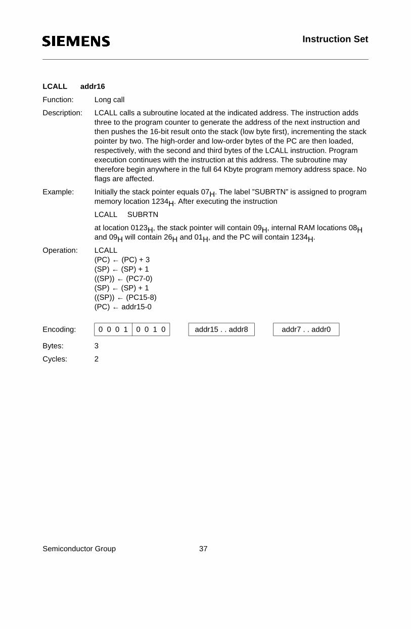
LCALL addr16
Function: Long call
Description: LCALL calls a subroutine located at the indicated address. The instruction adds three to the program counter to generate the address of the next instruction and then pushes the 16-bit result onto the stack (low byte first), incrementing the stack pointer by two. The high-order and low-order bytes of the PC are then loaded, respectively, with the second and third bytes of the LCALL instruction. Program execution continues with the instruction at this address. The subroutine may therefore begin anywhere in the full 64 Kbyte program memory address space. No
Semiconductor Group 37
flags are affected.
Example: Initially the stack pointer equals 07H. The label ”SUBRTN” is assigned to program memory location 1234H. After executing the instruction
LCALL SUBRTN
at location 0123H, the stack pointer will contain 09H, internal RAM locations 08H and 09H will contain 26H and 01H, and the PC will contain 1234H.
Operation: LCALL(PC) ← (PC) + 3(SP) ← (SP) + 1((SP)) ← (PC7-0)(SP) ← (SP) + 1((SP)) ← (PC15-8)(PC) ← addr15-0
Bytes: 3
Cycles: 2
Encoding: 0 0 0 1 0 0 1 0 addr15 . . addr8 addr7 . . addr0
Instruction Set
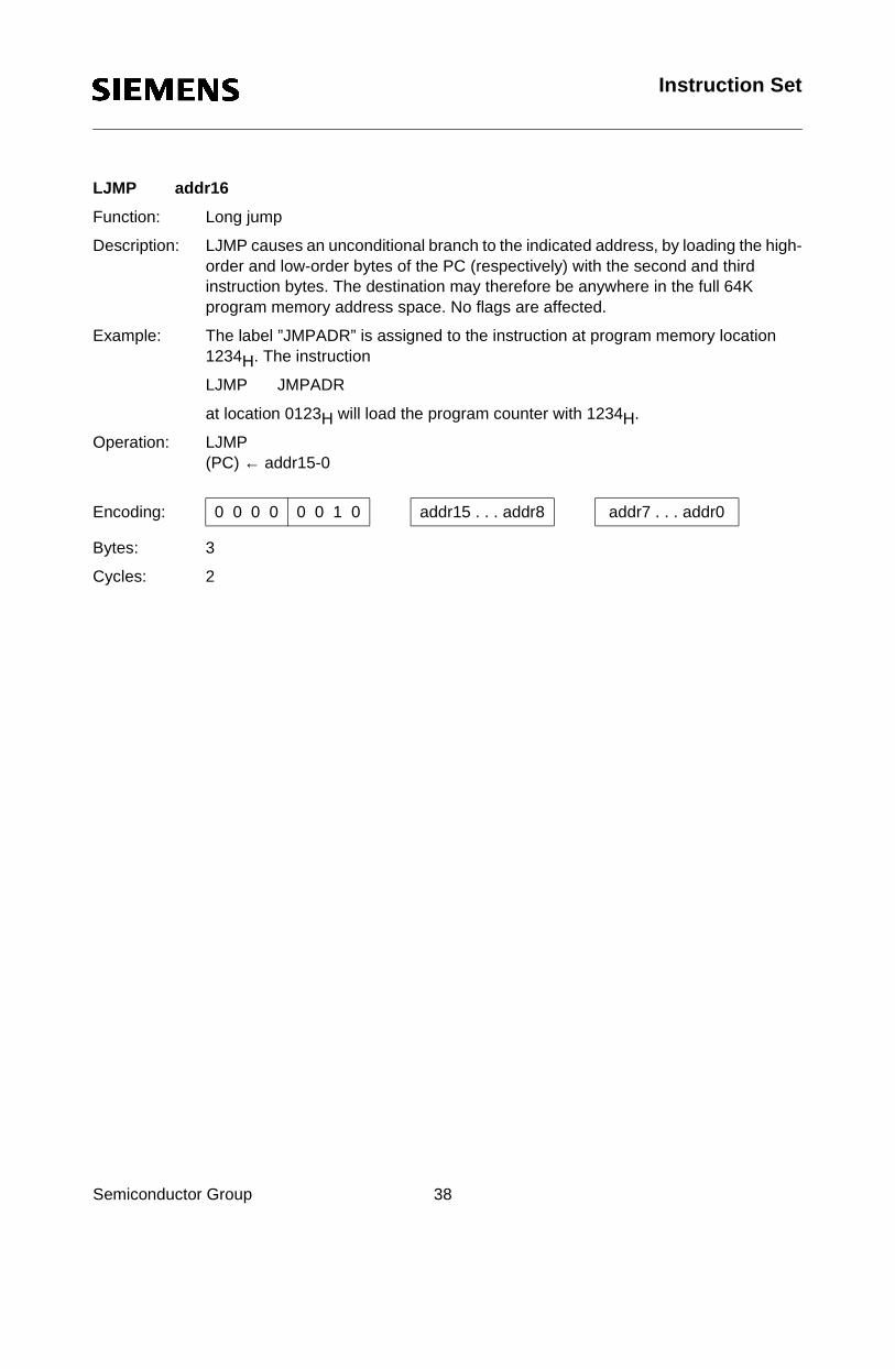
LJMP addr16
Function: Long jump
Description: LJMP causes an unconditional branch to the indicated address, by loading the high-order and low-order bytes of the PC (respectively) with the second and third instruction bytes. The destination may therefore be anywhere in the full 64K program memory address space. No flags are affected.
Example: The label ”JMPADR” is assigned to the instruction at program memory location 1234H. The instruction
LJMP JMPADR
Semiconductor Group 38
at location 0123H will load the program counter with 1234H.
Operation: LJMP(PC) ← addr15-0
Bytes: 3
Cycles: 2
Encoding: 0 0 0 0 0 0 1 0 addr15 . . . addr8 addr7 . . . addr0
Instruction Set
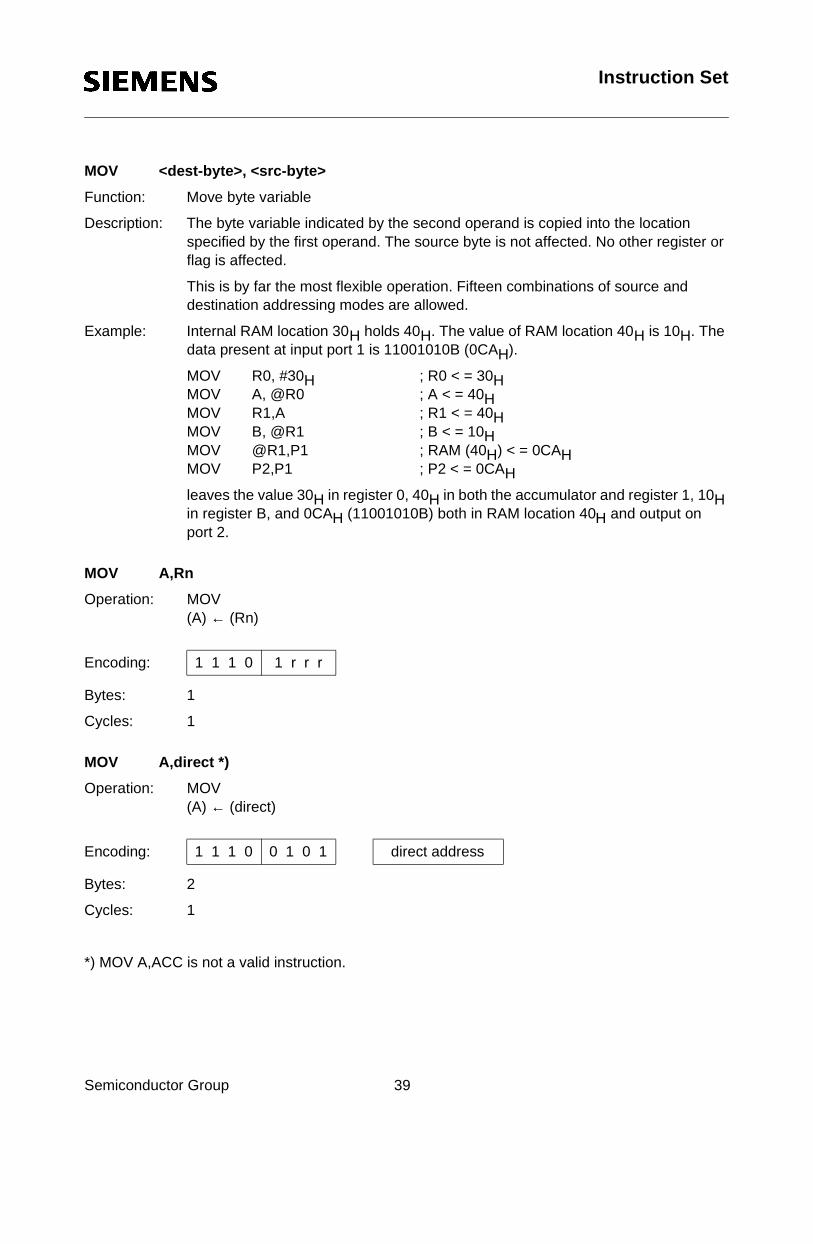
MOV <dest-byte>, <src-byte>
Function: Move byte variable
Description: The byte variable indicated by the second operand is copied into the location specified by the first operand. The source byte is not affected. No other register or flag is affected.
This is by far the most flexible operation. Fifteen combinations of source and destination addressing modes are allowed.
Example: Internal RAM location 30H holds 40H. The value of RAM location 40H is 10H. The data present at input port 1 is 11001010B (0CA ).
Semiconductor Group 39
HMOV R0, #30H ; R0 < = 30HMOV A, @R0 ; A < = 40HMOV R1,A ; R1 < = 40HMOV B, @R1 ; B < = 10HMOV @R1,P1 ; RAM (40H) < = 0CAHMOV P2,P1 ; P2 < = 0CAH
leaves the value 30H in register 0, 40H in both the accumulator and register 1, 10H in register B, and 0CAH (11001010B) both in RAM location 40H and output on port 2.
MOV A,Rn
Operation: MOV(A) ← (Rn)
Bytes: 1
Cycles: 1
MOV A,direct *)
Operation: MOV(A) ← (direct)
Bytes: 2
Cycles: 1
*) MOV A,ACC is not a valid instruction.
Encoding: 1 1 1 0 1 r r r
Encoding: 1 1 1 0 0 1 0 1 direct address

Instruction Set
MOV A,@Ri
Operation: MOV(A) ← ((Ri))
Bytes: 1
Cycles: 1
Encoding: 1 1 1 0 0 1 1 i
Semiconductor Group 40
MOV A, #data
Operation: MOV(A) ← #data
Bytes: 2
Cycles: 1
MOV Rn,A
Operation: MOV(Rn) ← (A)
Bytes: 1
Cycles: 1
MOV Rn,direct
Operation: MOV(Rn) ← (direct)
Bytes: 2
Cycles: 2
Encoding: 0 1 1 1 0 1 0 0 immediate data
Encoding: 1 1 1 1 1 r r r
Encoding: 1 0 1 0 1 r r r direct address

Instruction Set
MOV Rn, #data
Operation: MOV(Rn) ← #data
Bytes: 2
Cycles: 1
Encoding: 0 1 1 1 1 r r r immediate data
Semiconductor Group 41
MOV direct,A
Operation: MOV(direct) ← (A)
Bytes: 2
Cycles: 1
MOV direct,Rn
Operation: MOV(direct) ← (Rn)
Bytes: 2
Cycles: 2
MOV direct,direct
Operation: MOV(direct) ← (direct)
Bytes: 3
Cycles: 2
Encoding: 1 1 1 1 0 1 0 1 direct address
Encoding: 1 0 0 0 1 r r r direct address
Encoding: 1 0 0 0 0 1 0 1 dir.addr. (src) dir.addr. (dest)
Instruction Set
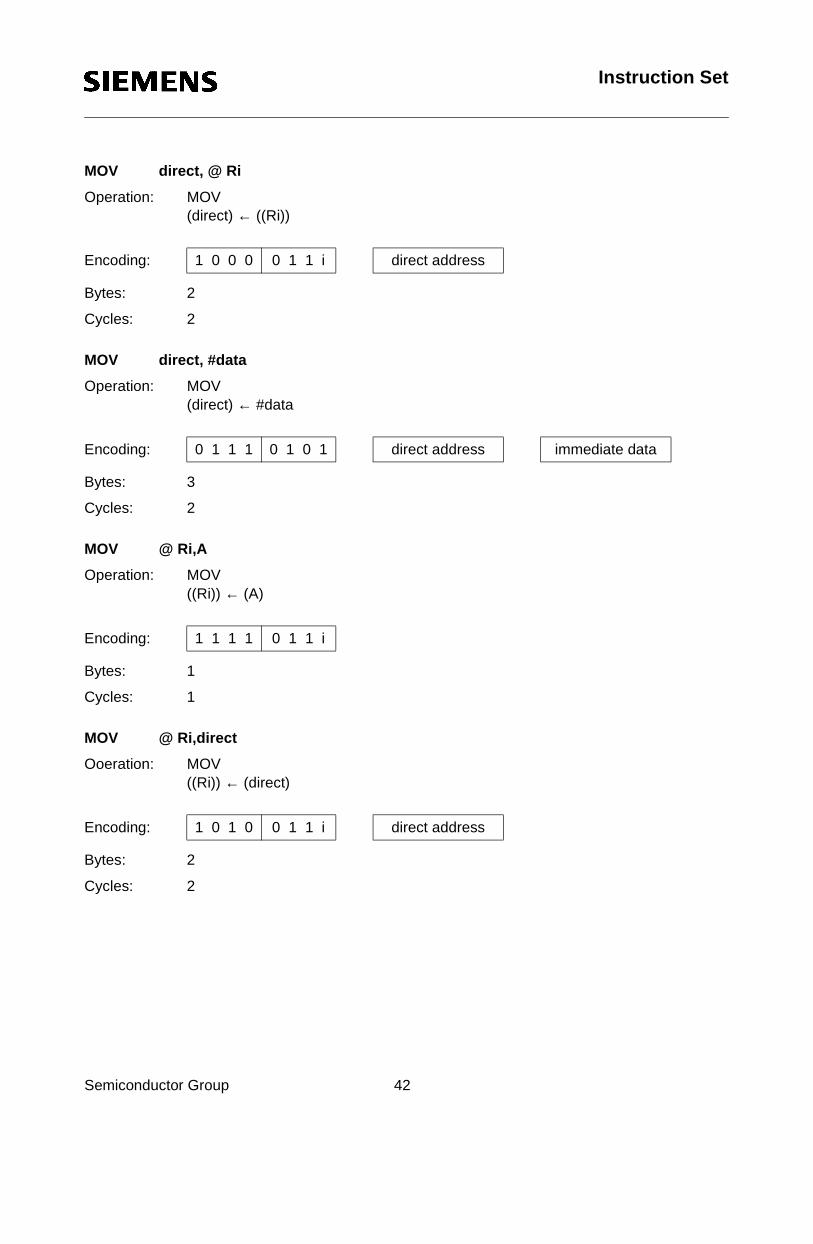
MOV direct, @ Ri
Operation: MOV(direct) ← ((Ri))
Bytes: 2
Cycles: 2
Encoding: 1 0 0 0 0 1 1 i direct address
Semiconductor Group 42
MOV direct, #data
Operation: MOV(direct) ← #data
Bytes: 3
Cycles: 2
MOV @ Ri,A
Operation: MOV((Ri)) ← (A)
Bytes: 1
Cycles: 1
MOV @ Ri,direct
Ooeration: MOV((Ri)) ← (direct)
Bytes: 2
Cycles: 2
Encoding: 0 1 1 1 0 1 0 1 direct address immediate data
Encoding: 1 1 1 1 0 1 1 i
Encoding: 1 0 1 0 0 1 1 i direct address
Instruction Set
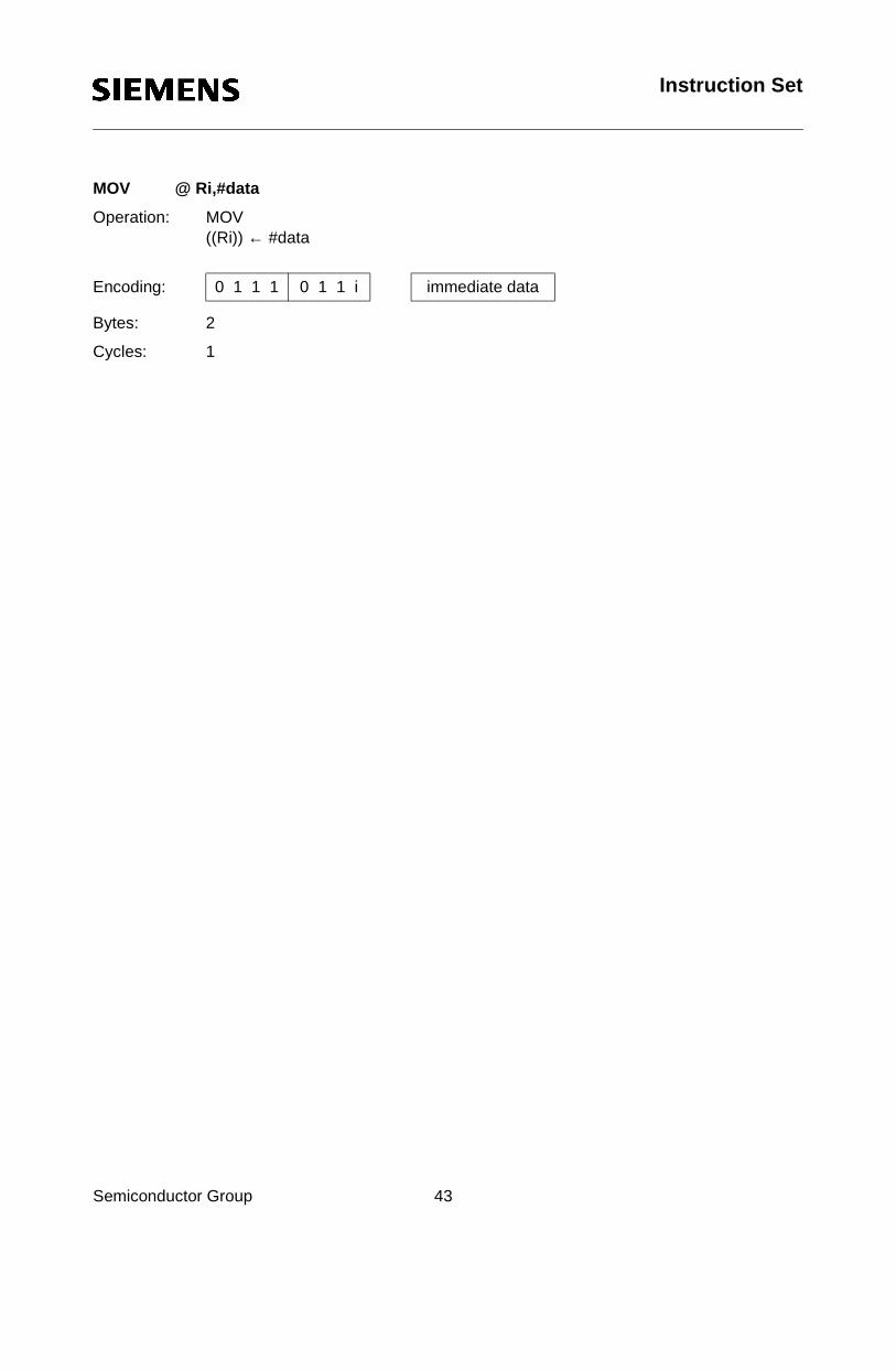
MOV @ Ri,#data
Operation: MOV((Ri)) ← #data
Bytes: 2
Cycles: 1
Encoding: 0 1 1 1 0 1 1 i immediate data
Semiconductor Group 43
Instruction Set
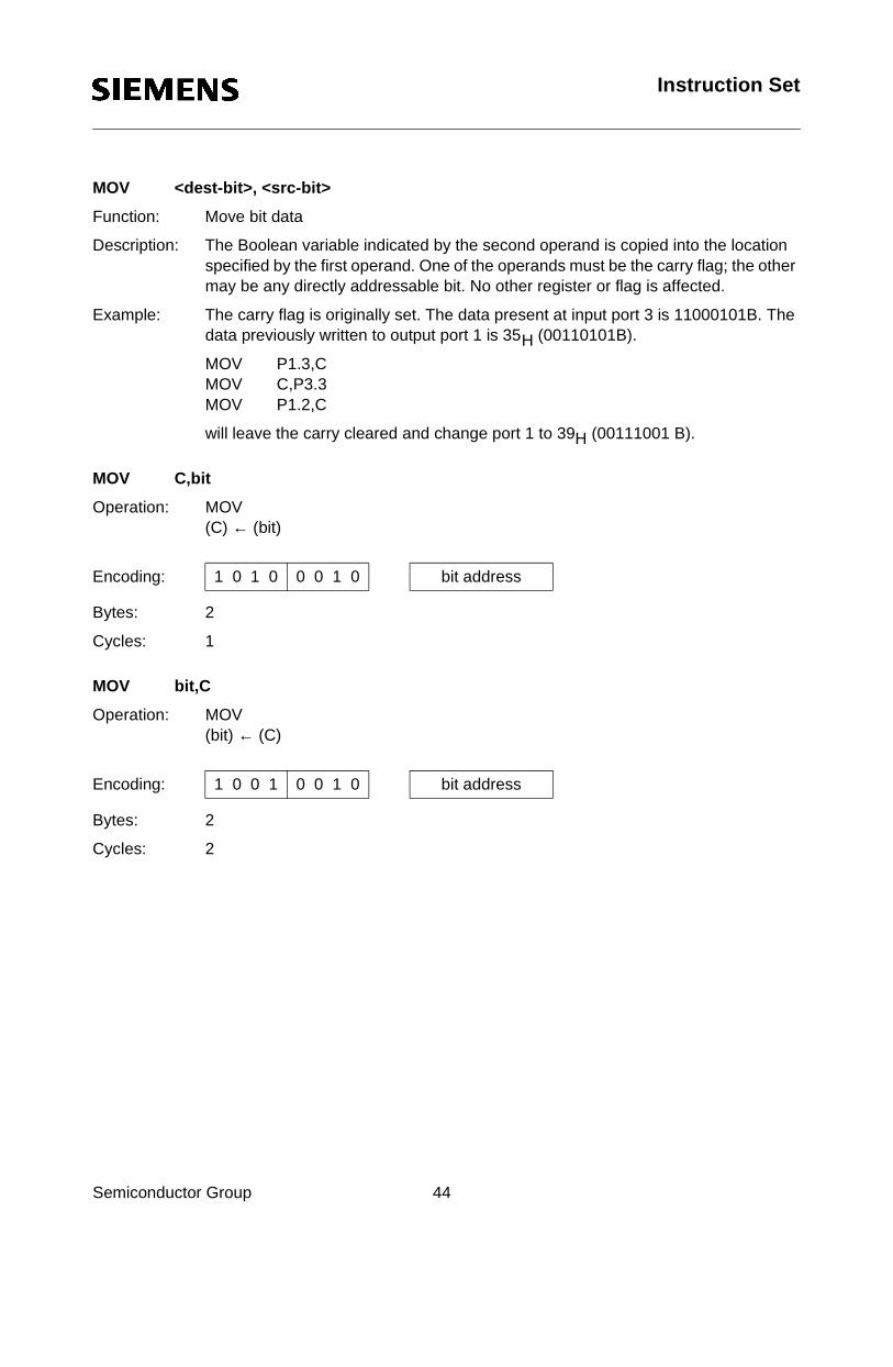
MOV <dest-bit>, <src-bit>
Function: Move bit data
Description: The Boolean variable indicated by the second operand is copied into the location specified by the first operand. One of the operands must be the carry flag; the other may be any directly addressable bit. No other register or flag is affected.
Example: The carry flag is originally set. The data present at input port 3 is 11000101B. The data previously written to output port 1 is 35H (00110101B).
MOV P1.3,CMOV C,P3.3
Semiconductor Group 44
MOV P1.2,C
will leave the carry cleared and change port 1 to 39H (00111001 B).
MOV C,bit
Operation: MOV(C) ← (bit)
Bytes: 2
Cycles: 1
MOV bit,C
Operation: MOV(bit) ← (C)
Bytes: 2
Cycles: 2
Encoding: 1 0 1 0 0 0 1 0 bit address
Encoding: 1 0 0 1 0 0 1 0 bit address
Instruction Set
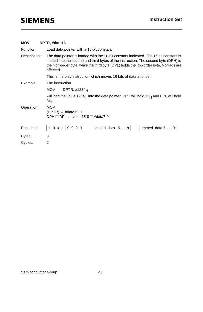
MOV DPTR, #data16
Function: Load data pointer with a 16-bit constant
Description: The data pointer is loaded with the 16-bit constant indicated. The 16 bit constant is loaded into the second and third bytes of the instruction. The second byte (DPH) is the high-order byte, while the third byte (DPL) holds the low-order byte. No flags are affected.
This is the only instruction which moves 16 bits of data at once.
Example: The instruction
Semiconductor Group 45
MOV DPTR, #1234Hwill load the value 1234H into the data pointer: DPH will hold 12H and DPL will hold 34H.
Operation: MOV(DPTR) ← #data15-0DPH DPL ← #data15-8 #data7-0
Bytes: 3
Cycles: 2
Encoding: 1 0 0 1 0 0 0 0 immed. data 15 . . . 8 immed. data 7 . . . 0
Instruction Set
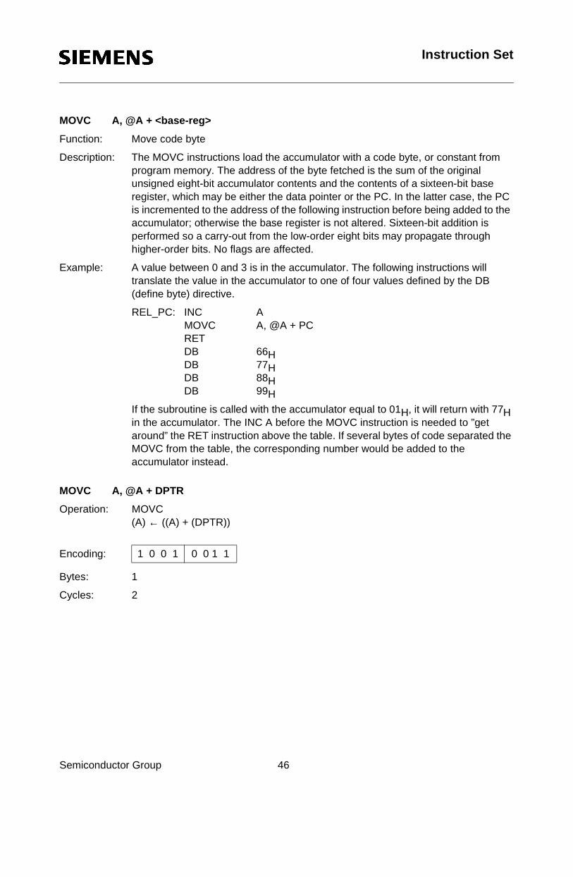
MOVC A, @A + <base-reg>
Function: Move code byte
Description: The MOVC instructions load the accumulator with a code byte, or constant from program memory. The address of the byte fetched is the sum of the original unsigned eight-bit accumulator contents and the contents of a sixteen-bit base register, which may be either the data pointer or the PC. In the latter case, the PC is incremented to the address of the following instruction before being added to the accumulator; otherwise the base register is not altered. Sixteen-bit addition is performed so a carry-out from the low-order eight bits may propagate through
Semiconductor Group 46
higher-order bits. No flags are affected.
Example: A value between 0 and 3 is in the accumulator. The following instructions will translate the value in the accumulator to one of four values defined by the DB (define byte) directive.
REL_PC: INC AMOVC A, @A + PCRETDB 66HDB 77HDB 88HDB 99H
If the subroutine is called with the accumulator equal to 01H, it will return with 77H in the accumulator. The INC A before the MOVC instruction is needed to ”get around” the RET instruction above the table. If several bytes of code separated the MOVC from the table, the corresponding number would be added to the accumulator instead.
MOVC A, @A + DPTR
Operation: MOVC(A) ← ((A) + (DPTR))
Bytes: 1
Cycles: 2
Encoding: 1 0 0 1 0 0 1 1

Instruction Set
MOVC A, @A + PC
Operation: MOVC(PC) ← (PC) + 1(A) ← ((A) + (PC))
Bytes: 1
Cycles: 2
Encoding: 1 0 0 0 0 0 1 1
Semiconductor Group 47

Instruction Set
MOVX <dest-byte>, <src-byte>
Function: Move external
Description: The MOVX instructions transfer data between the accumulator and a byte of external data memory, hence the ”X” appended to MOV. There are two types of instructions, differing in whether they provide an eight bit or sixteen-bit indirect address to the external data RAM.
In the first type, the contents of R0 or R1 in the current register bank provide an eight-bit address multiplexed with data on P0. Eight bits are sufficient for externall/O expansion decoding or a relatively small RAM array. For somewhat larger
Semiconductor Group 48
arrays, any output port pins can be used to output higher-order address bits. These pins would be controlled by an output instruction preceding the MOVX.
In the second type of MOVX instructions, the data pointer generates a sixteen-bit address. P2 outputs the high-order eight address bits (the contents of DPH) while P0 multiplexes the low-order eight bits (DPL) with data. The P2 special function register retains its previous contents while the P2 output buffers are emitting the contents of DPH. This form is faster and more efficient when accessing very large data arrays (up to 64 Kbyte), since no additional instructions are needed to set up the output ports.
It is possible in some situations to mix the two MOVX types. A large RAM array with its high-order address lines driven by P2 can be addressed via the data pointer, or with code to output high-order address bits to P2 followed by a MOVX instruction using R0 or R1.
Example: An external 256 byte RAM using multiplexed address/data lines (e.g. an SAB 8155 RAM/I/O/timer) is connected to the SAB 80(c)5XX port 0. Port 3 provides control lines for the external RAM. Ports 1 and 2 are used for normal l/O. Registers 0 and 1 contain 12H and 34H. Location 34H of the external RAM holds the value 56H. The instruction sequence
MOVX A, @R1MOVX @R0,A
copies the value 56H into both the accumulator and external RAM location 12H.
Instruction Set
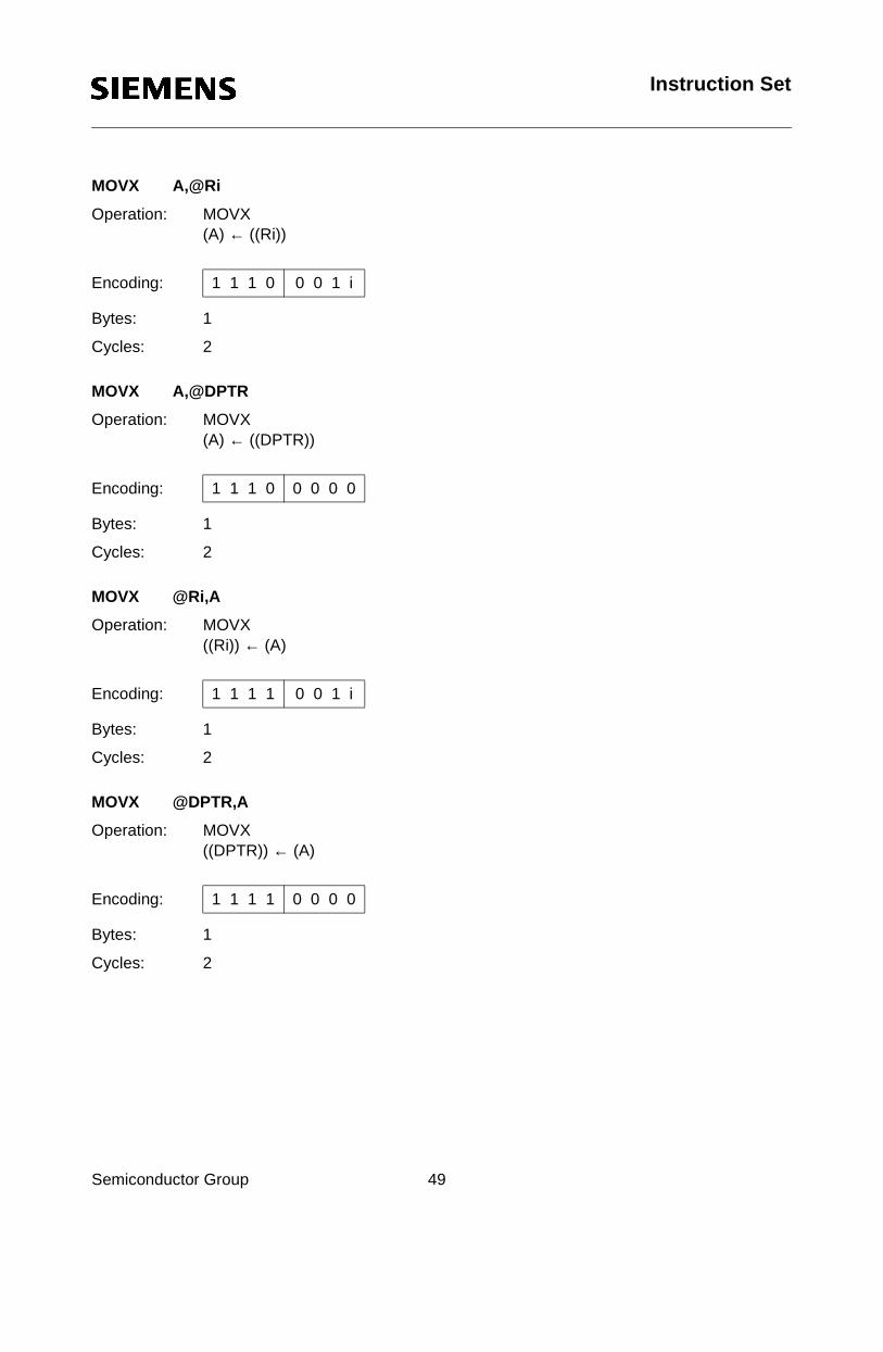
MOVX A,@Ri
Operation: MOVX(A) ← ((Ri))
Bytes: 1
Cycles: 2
Encoding: 1 1 1 0 0 0 1 i
Semiconductor Group 49
MOVX A,@DPTR
Operation: MOVX(A) ← ((DPTR))
Bytes: 1
Cycles: 2
MOVX @Ri,A
Operation: MOVX((Ri)) ← (A)
Bytes: 1
Cycles: 2
MOVX @DPTR,A
Operation: MOVX((DPTR)) ← (A)
Bytes: 1
Cycles: 2
Encoding: 1 1 1 0 0 0 0 0
Encoding: 1 1 1 1 0 0 1 i
Encoding: 1 1 1 1 0 0 0 0
Instruction Set
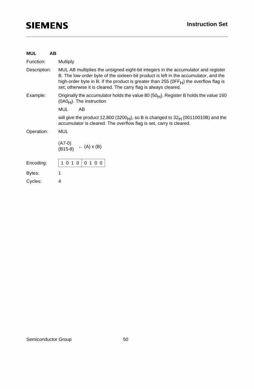
MUL AB
Function: Multiply
Description: MUL AB multiplies the unsigned eight-bit integers in the accumulator and register B. The low-order byte of the sixteen-bit product is left in the accumulator, and the high-order byte in B. If the product is greater than 255 (0FFH) the overflow flag is set; otherwise it is cleared. The carry flag is always cleared.
Example: Originally the accumulator holds the value 80 (50H). Register B holds the value 160 (0A0H). The instruction
MUL AB
Semiconductor Group 50
will give the product 12,800 (3200H), so B is changed to 32H (00110010B) and the accumulator is cleared. The overflow flag is set, carry is cleared.
Operation: MUL
(A7-0)(B15-8)
Bytes: 1
Cycles: 4
Encoding: 1 0 1 0 0 1 0 0
← (A) x (B)
Instruction Set
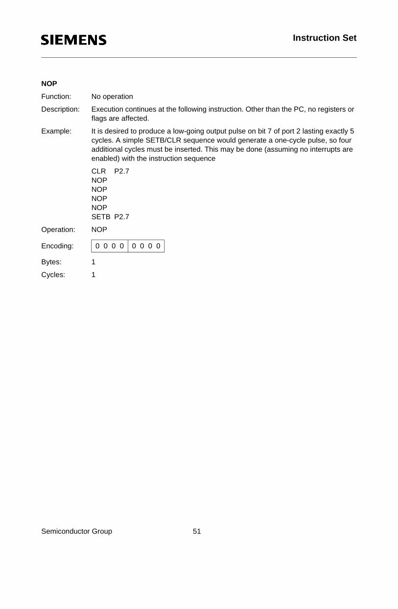
NOP
Function: No operation
Description: Execution continues at the following instruction. Other than the PC, no registers or flags are affected.
Example: It is desired to produce a low-going output pulse on bit 7 of port 2 lasting exactly 5 cycles. A simple SETB/CLR sequence would generate a one-cycle pulse, so four additional cycles must be inserted. This may be done (assuming no interrupts are enabled) with the instruction sequence
CLR P2.7
Semiconductor Group 51
NOPNOPNOPNOPSETB P2.7
Operation: NOP
Bytes: 1
Cycles: 1
Encoding: 0 0 0 0 0 0 0 0
Instruction Set
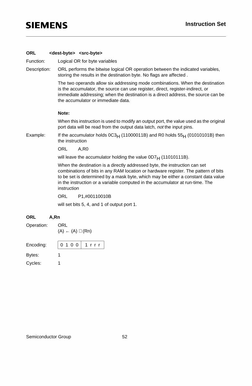
ORL <dest-byte> <src-byte>
Function: Logical OR for byte variables
Description: ORL performs the bitwise logical OR operation between the indicated variables, storing the results in the destination byte. No flags are affected .
The two operands allow six addressing mode combinations. When the destination is the accumulator, the source can use register, direct, register-indirect, or immediate addressing; when the destination is a direct address, the source can be the accumulator or immediate data.
Semiconductor Group 52
Note:
When this instruction is used to modify an output port, the value used as the original port data will be read from the output data latch, not the input pins.
Example: If the accumulator holds 0C3H (11000011B) and R0 holds 55H (01010101B) then the instruction
ORL A,R0
will leave the accumulator holding the value 0D7H (11010111B).
When the destination is a directly addressed byte, the instruction can set combinations of bits in any RAM location or hardware register. The pattern of bits to be set is determined by a mask byte, which may be either a constant data value in the instruction or a variable computed in the accumulator at run-time. The instruction
ORL P1,#00110010B
will set bits 5, 4, and 1 of output port 1.
ORL A,Rn
Operation: ORL(A) ← (A) ∨ (Rn)
Bytes: 1
Cycles: 1
Encoding: 0 1 0 0 1 r r r
Instruction Set
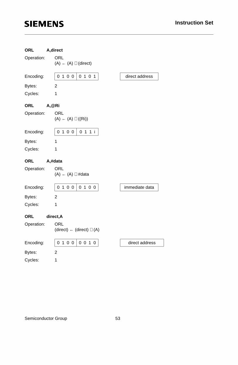
ORL A,direct
Operation: ORL(A) ← (A) ∨ (direct)
Bytes: 2
Cycles: 1
Encoding: 0 1 0 0 0 1 0 1 direct address
Semiconductor Group 53
ORL A,@Ri
Operation: ORL(A) ← (A) ∨ ((Ri))
Bytes: 1
Cycles: 1
ORL A,#data
Operation: ORL(A) ← (A) ∨ #data
Bytes: 2
Cycles: 1
ORL direct,A
Operation: ORL(direct) ← (direct) ∨ (A)
Bytes: 2
Cycles: 1
Encoding: 0 1 0 0 0 1 1 i
Encoding: 0 1 0 0 0 1 0 0 immediate data
Encoding: 0 1 0 0 0 0 1 0 direct address

Instruction Set
ORL direct, #data
Operation: ORL(direct) ← (direct) ∨ #data
Bytes: 3
Cycles: 2
Encoding: 0 1 0 0 0 0 1 1 direct address immediate data
Semiconductor Group 54
Instruction Set
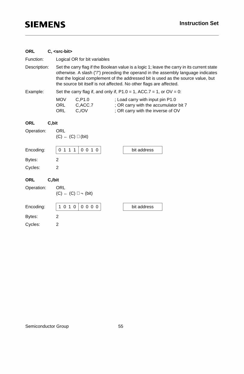
ORL C, <src-bit>
Function: Logical OR for bit variables
Description: Set the carry flag if the Boolean value is a logic 1; leave the carry in its current state otherwise. A slash (”/”) preceding the operand in the assembly language indicates that the logical complement of the addressed bit is used as the source value, but the source bit itself is not affected. No other flags are affected.
Example: Set the carry flag if, and only if, P1.0 = 1, ACC.7 = 1, or OV = 0:
MOV C,P1.0 ; Load carry with input pin P1.0ORL C,ACC.7 ; OR carry with the accumulator bit 7
Semiconductor Group 55
ORL C,/OV ; OR carry with the inverse of OV
ORL C,bit
Operation: ORL(C) ← (C) ∨ (bit)
Bytes: 2
Cycles: 2
ORL C,/bit
Operation: ORL(C) ← (C) ∨ ¬ (bit)
Bytes: 2
Cycles: 2
Encoding: 0 1 1 1 0 0 1 0 bit address
Encoding: 1 0 1 0 0 0 0 0 bit address
Instruction Set
POP direct
Function: Pop from stack
Description: The contents of the internal RAM location addressed by the stack pointer is read, and the stack pointer is decremented by one. The value read is the transfer to the directly addressed byte indicated. No flags are affected.
Example: The stack pointer originally contains the value 32H, and internal RAM locations 30H through 32H contain the values 20H, 23H, and 01H, respectively. The instruction sequence
POP DPH
Semiconductor Group 56
POP DPL
will leave the stack pointer equal to the value 30H and the data pointer set to 0123H. At this point the instruction
POP SP
will leave the stack pointer set to 20H. Note that in this special case the stack pointer was decremented to 2FH before being loaded with the value popped (20H).
Operation: POP(direct) ← ((SP))(SP) ← (SP) – 1
Bytes: 2
Cycles: 2
Encoding: 1 1 0 1 0 0 0 0 direct address
Instruction Set
PUSH direct
Function: Push onto stack
Description: The stack pointer is incremented by one. The contents of the indicated variable is then copied into the internal RAM location addressed by the stack pointer. Otherwise no flags are affected.
Example: On entering an interrupt routine the stack pointer contains 09H. The data pointer holds the value 0123H. The instruction sequence
PUSH DPLPUSH DPH
Semiconductor Group 57
will leave the stack pointer set to 0BH and store 23H and 01H in internal RAM locations 0AH and 0BH, respectively.
Operation: PUSH(SP) ← (SP) + 1((SP)) ← (direct)
Bytes: 2
Cycles: 2
Encoding: 1 1 0 0 0 0 0 0 direct address
Instruction Set
RET
Function: Return from subroutine
Description: RET pops the high and low-order bytes of the PC successively from the stack, decrementing the stack pointer by two. Program execution continues at the resulting address, generally the instruction immediately following an ACALL or LCALL. No flags are affected.
Example: The stack pointer originally contains the value 0BH. Internal RAM locations 0AH and 0BH contain the values 23H and 01H, respectively. The instruction
Semiconductor Group 58
RET
will leave the stack pointer equal to the value 09H. Program execution will continue at location 0123H.
Operation: RET(PC15-8) ← ((SP))(SP) ← (SP) – 1(PC7-0) ← ((SP))(SP) ← (SP) – 1
Bytes: 1
Cycles: 2
Encoding: 0 0 1 0 0 0 1 0
Instruction Set
RETI
Function: Return from interrupt
Description: RETI pops the high and low-order bytes of the PC successively from the stack, and restores the interrupt logic to accept additional interrupts at the same priority level as the one just processed. The stack pointer is left decremented by two. No other registers are affected; the PSW is not automatically restored to its pre-interrupt status. Program execution continues at the resulting address, which is generally the instruction immediately after the point at which the interrupt request was detected. If a lower or same-level interrupt is pending when the RETI instruction is executed,
Semiconductor Group 59
that one instruction will be executed before the pending interrupt is processed.
Example: The stack pointer originally contains the value 0BH. An interrupt was detected during the instruction ending at location 0122H. Internal RAM locations 0AH and 0BH contain the values 23H and 01H, respectively. The instruction
RETI
will leave the stack pointer equal to 09H and return program execution to location 0123H.
Operation: RETI(PC15-8) ← ((SP))(SP) ← (SP) – 1(PC7-0) ← ((SP))(SP) ← (SP) – 1
Bytes: 1
Cycles: 2
Encoding: 0 0 1 1 0 0 1 0
Instruction Set
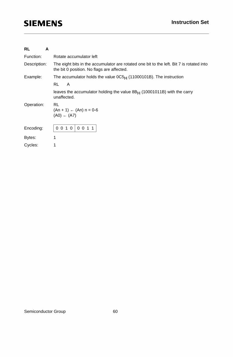
RL A
Function: Rotate accumulator left
Description: The eight bits in the accumulator are rotated one bit to the left. Bit 7 is rotated into the bit 0 position. No flags are affected.
Example: The accumulator holds the value 0C5H (11000101B). The instruction
RL A
leaves the accumulator holding the value 8BH (10001011B) with the carry unaffected.
Semiconductor Group 60
Operation: RL(An + 1) ← (An) n = 0-6(A0) ← (A7)
Bytes: 1
Cycles: 1
Encoding: 0 0 1 0 0 0 1 1
Instruction Set
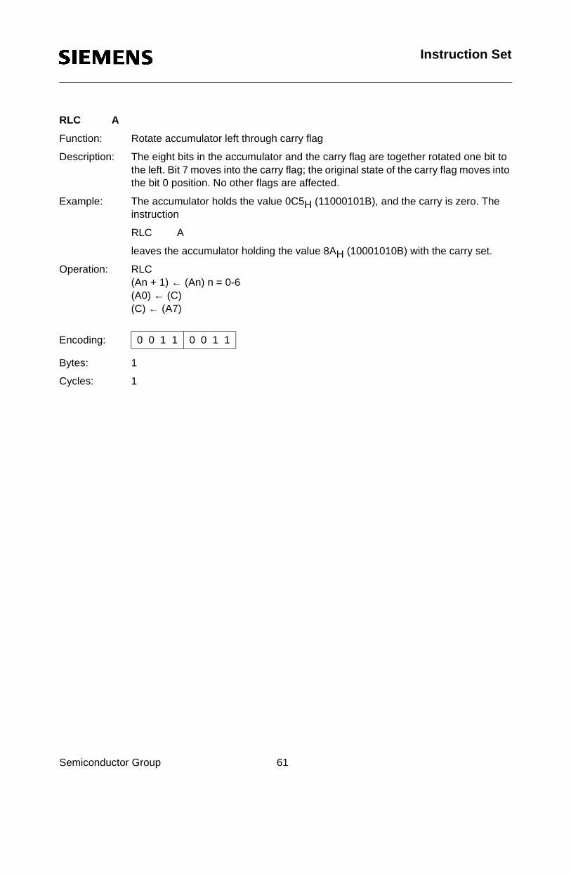
RLC A
Function: Rotate accumulator left through carry flag
Description: The eight bits in the accumulator and the carry flag are together rotated one bit to the left. Bit 7 moves into the carry flag; the original state of the carry flag moves into the bit 0 position. No other flags are affected.
Example: The accumulator holds the value 0C5H (11000101B), and the carry is zero. The instruction
RLC A
Semiconductor Group 61
leaves the accumulator holding the value 8AH (10001010B) with the carry set.
Operation: RLC(An + 1) ← (An) n = 0-6(A0) ← (C)(C) ← (A7)
Bytes: 1
Cycles: 1
Encoding: 0 0 1 1 0 0 1 1
Instruction Set
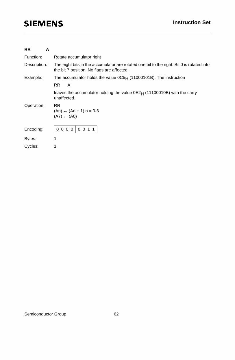
RR A
Function: Rotate accumulator right
Description: The eight bits in the accumulator are rotated one bit to the right. Bit 0 is rotated into the bit 7 position. No flags are affected.
Example: The accumulator holds the value 0C5H (11000101B). The instruction
RR A
leaves the accumulator holding the value 0E2H (11100010B) with the carry unaffected.
Semiconductor Group 62
Operation: RR(An) ← (An + 1) n = 0-6(A7) ← (A0)
Bytes: 1
Cycles: 1
Encoding: 0 0 0 0 0 0 1 1
Instruction Set
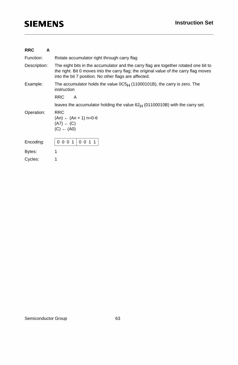
RRC A
Function: Rotate accumulator right through carry flag
Description: The eight bits in the accumulator and the carry flag are together rotated one bit to the right. Bit 0 moves into the carry flag; the original value of the carry flag moves into the bit 7 position. No other flags are affected.
Example: The accumulator holds the value 0C5H (11000101B), the carry is zero. The instruction
RRC A
Semiconductor Group 63
leaves the accumulator holding the value 62H (01100010B) with the carry set.
Operation: RRC(An) ← (An + 1) n=0-6(A7) ← (C)(C) ← (A0)
Bytes: 1
Cycles: 1
Encoding: 0 0 0 1 0 0 1 1
Instruction Set
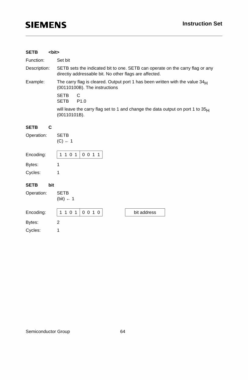
SETB <bit>
Function: Set bit
Description: SETB sets the indicated bit to one. SETB can operate on the carry flag or any directiy addressable bit. No other flags are affected.
Example: The carry flag is cleared. Output port 1 has been written with the value 34H (00110100B). The instructions
SETB CSETB P1.0
Semiconductor Group 64
will leave the carry flag set to 1 and change the data output on port 1 to 35H (00110101B).
SETB C
Operation: SETB(C) ← 1
Bytes: 1
Cycles: 1
SETB bit
Operation: SETB(bit) ← 1
Bytes: 2
Cycles: 1
Encoding: 1 1 0 1 0 0 1 1
Encoding: 1 1 0 1 0 0 1 0 bit address
Instruction Set
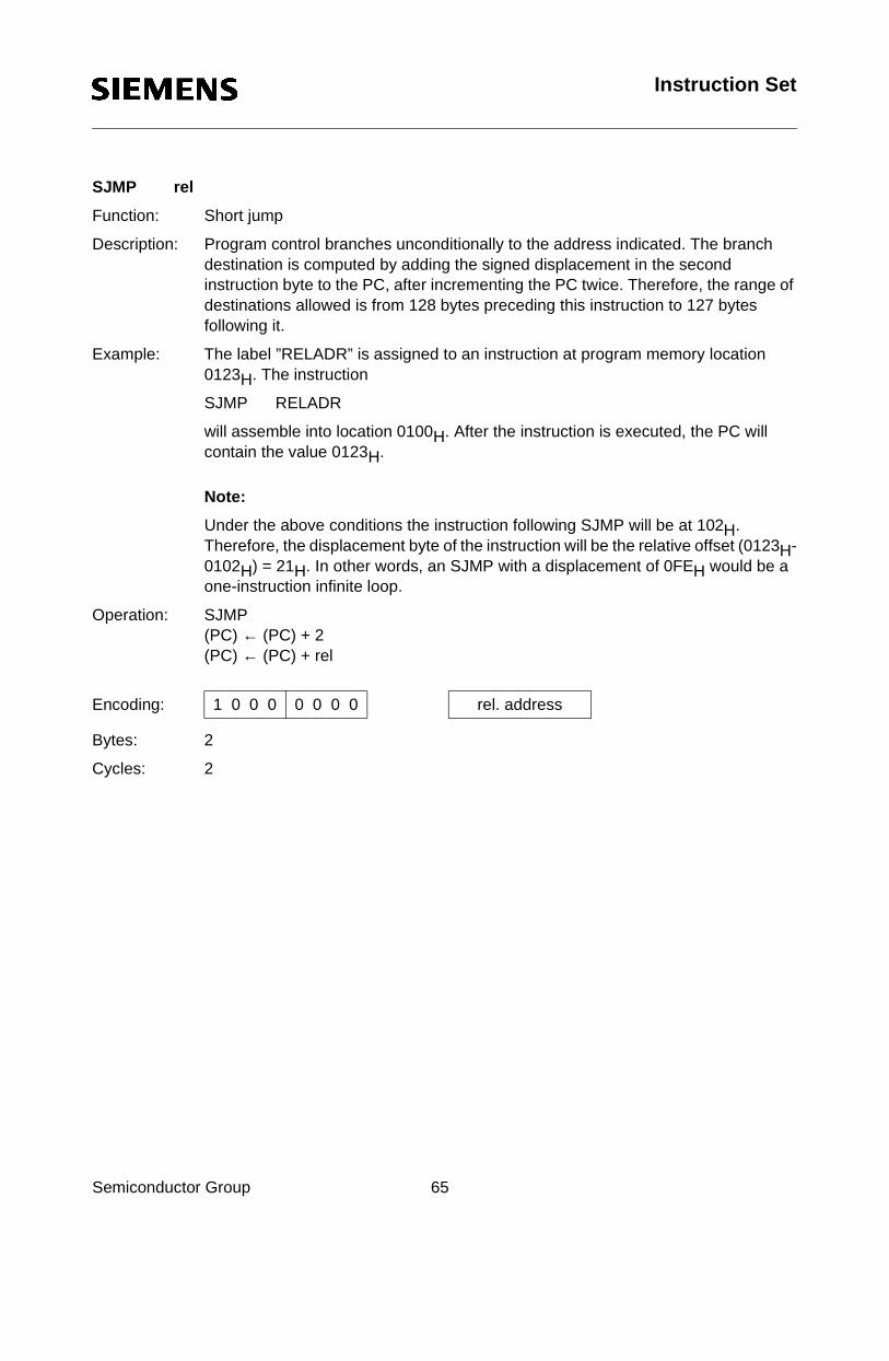
SJMP rel
Function: Short jump
Description: Program control branches unconditionally to the address indicated. The branch destination is computed by adding the signed displacement in the second instruction byte to the PC, after incrementing the PC twice. Therefore, the range of destinations allowed is from 128 bytes preceding this instruction to 127 bytes following it.
Example: The label ”RELADR” is assigned to an instruction at program memory location 0123H. The instruction
Semiconductor Group 65
SJMP RELADR
will assemble into location 0100H. After the instruction is executed, the PC will contain the value 0123H.
Note:
Under the above conditions the instruction following SJMP will be at 102H. Therefore, the displacement byte of the instruction will be the relative offset (0123H-0102H) = 21H. In other words, an SJMP with a displacement of 0FEH would be a one-instruction infinite loop.
Operation: SJMP(PC) ← (PC) + 2(PC) ← (PC) + rel
Bytes: 2
Cycles: 2
Encoding: 1 0 0 0 0 0 0 0 rel. address
Instruction Set
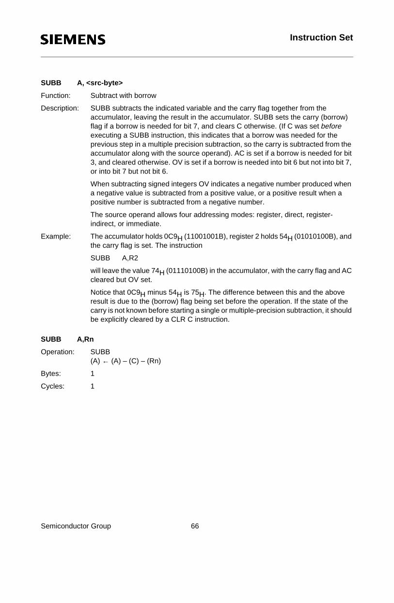
SUBB A, <src-byte>
Function: Subtract with borrow
Description: SUBB subtracts the indicated variable and the carry flag together from the accumulator, leaving the result in the accumulator. SUBB sets the carry (borrow) flag if a borrow is needed for bit 7, and clears C otherwise. (If C was set before executing a SUBB instruction, this indicates that a borrow was needed for the previous step in a multiple precision subtraction, so the carry is subtracted from the accumulator along with the source operand). AC is set if a borrow is needed for bit 3, and cleared otherwise. OV is set if a borrow is needed into bit 6 but not into bit 7,
Semiconductor Group 66
or into bit 7 but not bit 6.
When subtracting signed integers OV indicates a negative number produced when a negative value is subtracted from a positive value, or a positive result when a positive number is subtracted from a negative number.
The source operand allows four addressing modes: register, direct, register-indirect, or immediate.
Example: The accumulator holds 0C9H (11001001B), register 2 holds 54H (01010100B), and the carry flag is set. The instruction
SUBB A,R2
will leave the value 74H (01110100B) in the accumulator, with the carry flag and AC cleared but OV set.
Notice that 0C9H minus 54H is 75H. The difference between this and the above result is due to the (borrow) flag being set before the operation. If the state of the carry is not known before starting a single or multiple-precision subtraction, it should be explicitly cleared by a CLR C instruction.
SUBB A,Rn
Operation: SUBB(A) ← (A) – (C) – (Rn)
Bytes: 1
Cycles: 1
Instruction Set
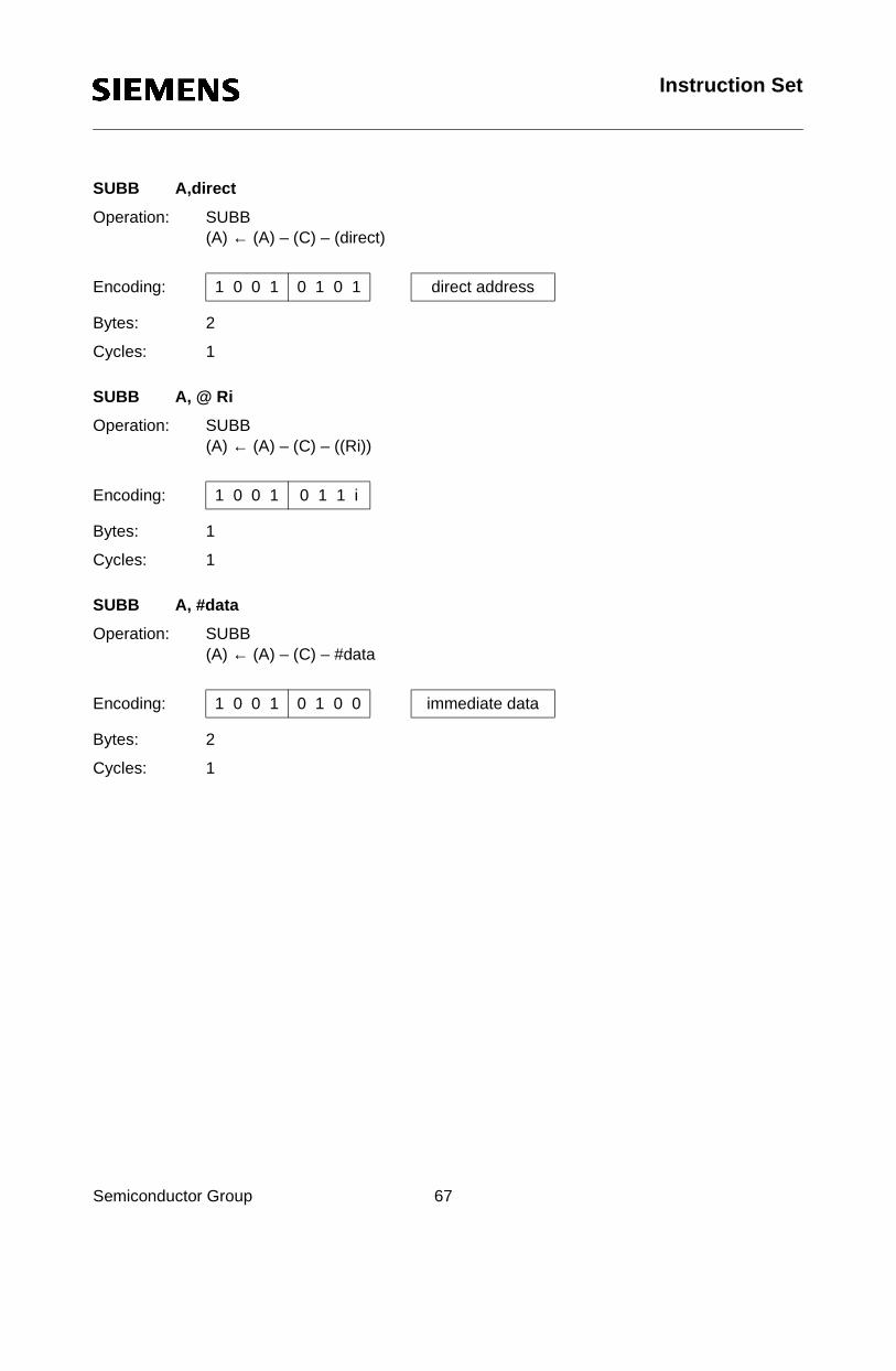
SUBB A,direct
Operation: SUBB(A) ← (A) – (C) – (direct)
Bytes: 2
Cycles: 1
Encoding: 1 0 0 1 0 1 0 1 direct address
Semiconductor Group 67
SUBB A, @ Ri
Operation: SUBB(A) ← (A) – (C) – ((Ri))
Bytes: 1
Cycles: 1
SUBB A, #data
Operation: SUBB(A) ← (A) – (C) – #data
Bytes: 2
Cycles: 1
Encoding: 1 0 0 1 0 1 1 i
Encoding: 1 0 0 1 0 1 0 0 immediate data
Instruction Set
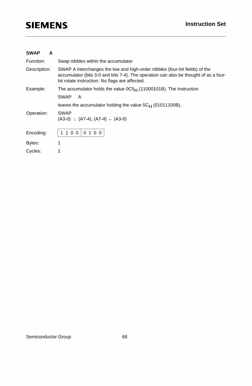
SWAP A
Function: Swap nibbles within the accumulator
Description: SWAP A interchanges the low and high-order nibbles (four-bit fields) of the accumulator (bits 3-0 and bits 7-4). The operation can also be thought of as a four-bit rotate instruction. No flags are affected.
Example: The accumulator holds the value 0C5H (11000101B). The instruction
SWAP A
leaves the accumulator holding the value 5CH (01011100B).
Semiconductor Group 68
Operation: SWAP(A3-0) (A7-4), (A7-4) ← (A3-0)
Bytes: 1
Cycles: 1
Encoding: 1 1 0 0 0 1 0 0
←→
Instruction Set
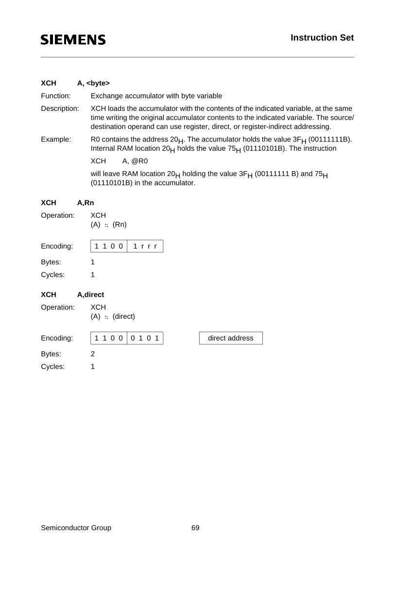
XCH A, <byte>
Function: Exchange accumulator with byte variable
Description: XCH loads the accumulator with the contents of the indicated variable, at the same time writing the original accumulator contents to the indicated variable. The source/destination operand can use register, direct, or register-indirect addressing.
Example: R0 contains the address 20H. The accumulator holds the value 3FH (00111111B). Internal RAM location 20H holds the value 75H (01110101B). The instruction
XCH A, @R0
Semiconductor Group 69
will leave RAM location 20H holding the value 3FH (00111111 B) and 75H (01110101B) in the accumulator.
XCH A,Rn
Operation: XCH(A) (Rn)
Bytes: 1
Cycles: 1
XCH A,direct
Operation: XCH(A) (direct)
Bytes: 2
Cycles: 1
Encoding: 1 1 0 0 1 r r r
Encoding: 1 1 0 0 0 1 0 1 direct address
←→
←→
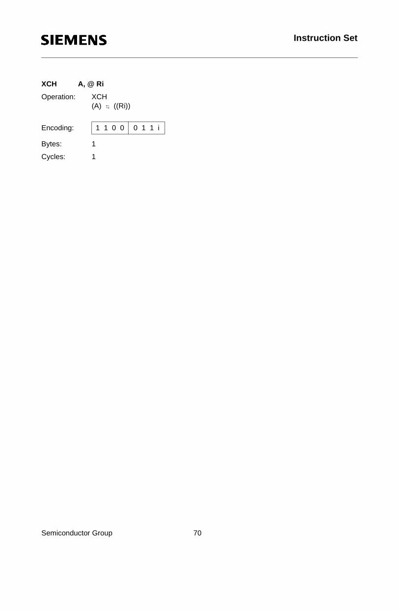
Instruction Set
XCH A, @ Ri
Operation: XCH(A) ((Ri))
Bytes: 1
Cycles: 1
Encoding: 1 1 0 0 0 1 1 i
←→
Semiconductor Group 70
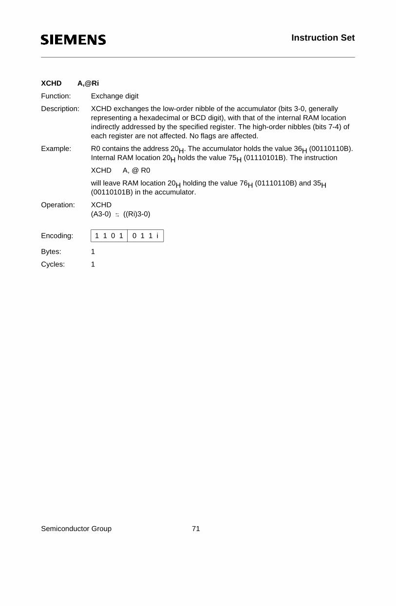
Instruction Set
XCHD A,@Ri
Function: Exchange digit
Description: XCHD exchanges the low-order nibble of the accumulator (bits 3-0, generally representing a hexadecimal or BCD digit), with that of the internal RAM location indirectly addressed by the specified register. The high-order nibbles (bits 7-4) of each register are not affected. No flags are affected.
Example: R0 contains the address 20H. The accumulator holds the value 36H (00110110B). Internal RAM location 20H holds the value 75H (01110101B). The instruction
XCHD A, @ R0
Semiconductor Group 71
will leave RAM location 20H holding the value 76H (01110110B) and 35H (00110101B) in the accumulator.
Operation: XCHD(A3-0) ((Ri)3-0)
Bytes: 1
Cycles: 1
Encoding: 1 1 0 1 0 1 1 i
←→
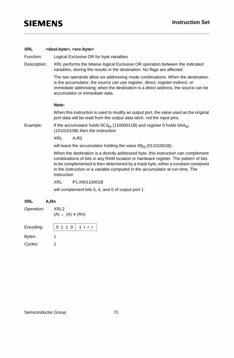
Instruction Set
XRL <dest-byte>, <src-byte>
Function: Logical Exclusive OR for byte variables
Description: XRL performs the bitwise logical Exclusive OR operation between the indicated variables, storing the results in the destination. No flags are affected.
The two operands allow six addressing mode combinations. When the destination is the accumulator, the source can use register, direct, register-indirect, or immediate addressing; when the destination is a direct address, the source can be accumulator or immediate data.
Semiconductor Group 72
Note:
When this instruction is used to modify an output port, the value used as the original port data will be read from the output data latch, not the input pins.
Example: If the accumulator holds 0C3H (11000011B) and register 0 holds 0AAH (10101010B) then the instruction
XRL A,R0
will leave the accumulator holding the value 69H (01101001B).
When the destination is a directly addressed byte, this instruction can complement combinations of bits in any RAM location or hardware register. The pattern of bits to be complemented is then determined by a mask byte, either a constant contained in the instruction or a variable computed in the accumulator at run-time. The instruction
XRL P1,#00110001B
will complement bits 5, 4, and 0 of output port 1.
XRL A,Rn
Operation: XRL2(A) ← (A) (Rn)
Bytes: 1
Cycles: 1
Encoding: 0 1 1 0 1 r r r
v
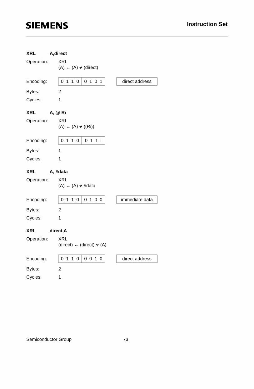
Instruction Set
XRL A,direct
Operation: XRL(A) ← (A) (direct)
Bytes: 2
Cycles: 1
Encoding: 0 1 1 0 0 1 0 1 direct address
v
Semiconductor Group 73
XRL A, @ Ri
Operation: XRL(A) ← (A) ((Ri))
Bytes: 1
Cycles: 1
XRL A, #data
Operation: XRL(A) ← (A) #data
Bytes: 2
Cycles: 1
XRL direct,A
Operation: XRL(direct) ← (direct) (A)
Bytes: 2
Cycles: 1
Encoding: 0 1 1 0 0 1 1 i
Encoding: 0 1 1 0 0 1 0 0 immediate data
Encoding: 0 1 1 0 0 0 1 0 direct address
v
v
v
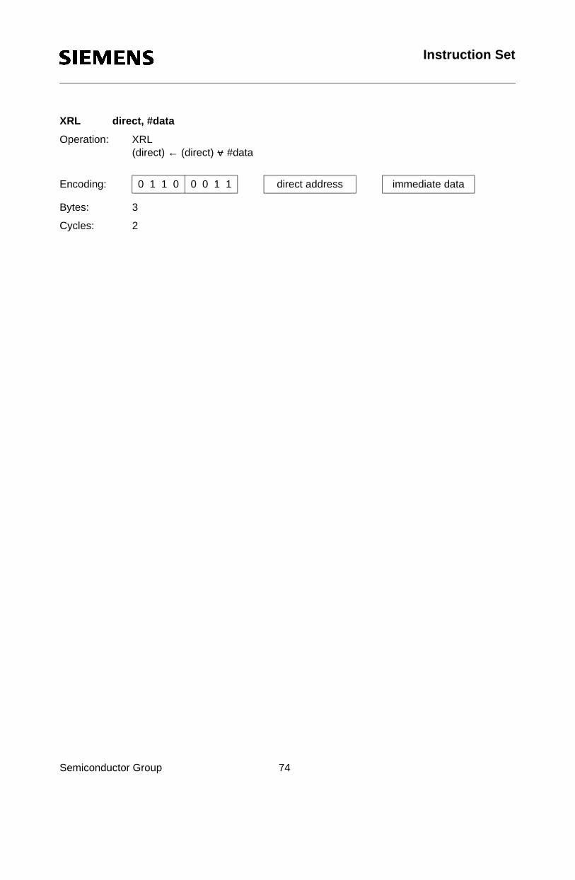
Instruction Set
XRL direct, #data
Operation: XRL(direct) ← (direct) #data
Bytes: 3
Cycles: 2
Encoding: 0 1 1 0 0 0 1 1 direct address immediate data
v
Semiconductor Group 74
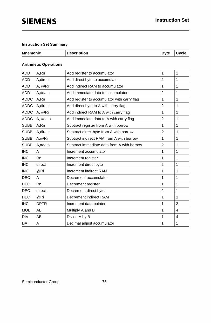
Instruction Set
Instruction Set Summary
Arithmetic Operations
Mnemonic Description Byte Cycle
ADD A,Rn Add register to accumulator 1 1
ADD A,direct Add direct byte to accumulator 2 1
ADD A, @Ri Add indirect RAM to accumulator 1 1
Semiconductor Group 75
ADD A,#data Add immediate data to accumulator 2 1
ADDC A,Rn Add register to accumulator with carry flag 1 1
ADDC A,direct Add direct byte to A with carry flag 2 1
ADDC A, @Ri Add indirect RAM to A with carry flag 1 1
ADDC A, #data Add immediate data to A with carry flag 2 1
SUBB A,Rn Subtract register from A with borrow 1 1
SUBB A,direct Subtract direct byte from A with borrow 2 1
SUBB A,@Ri Subtract indirect RAM from A with borrow 1 1
SUBB A,#data Subtract immediate data from A with borrow 2 1
INC A Increment accumulator 1 1
INC Rn Increment register 1 1
INC direct Increment direct byte 2 1
INC @Ri Increment indirect RAM 1 1
DEC A Decrement accumulator 1 1
DEC Rn Decrement register 1 1
DEC direct Decrement direct byte 2 1
DEC @Ri Decrement indirect RAM 1 1
INC DPTR Increment data pointer 1 2
MUL AB Multiply A and B 1 4
DIV AB Divide A by B 1 4
DA A Decimal adjust accumulator 1 1
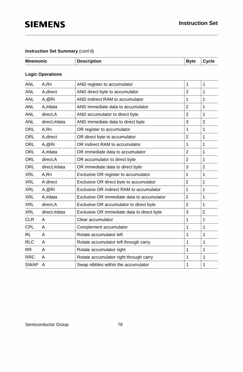
Instruction Set
Instruction Set Summary (cont’d)
Logic Operations
Mnemonic Description Byte Cycle
ANL A,Rn AND register to accumulator 1 1
ANL A,direct AND direct byte to accumulator 2 1
ANL A,@Ri AND indirect RAM to accumulator 1 1
Semiconductor Group 76
ANL A,#data AND immediate data to accumulator 2 1
ANL direct,A AND accumulator to direct byte 2 1
ANL direct,#data AND immediate data to direct byte 3 2
ORL A,Rn OR register to accumulator 1 1
ORL A,direct OR direct byte to accumulator 2 1
ORL A,@Ri OR indirect RAM to accumulator 1 1
ORL A,#data OR immediate data to accumulator 2 1
ORL direct,A OR accumulator to direct byte 2 1
ORL direct,#data OR immediate data to direct byte 3 2
XRL A,Rn Exclusive OR register to accumulator 1 1
XRL A direct Exclusive OR direct byte to accumulator 2 1
XRL A,@Ri Exclusive OR indirect RAM to accumulator 1 1
XRL A,#data Exclusive OR immediate data to accumulator 2 1
XRL direct,A Exclusive OR accumulator to direct byte 2 1
XRL direct,#data Exclusive OR immediate data to direct byte 3 2
CLR A Clear accumulator 1 1
CPL A Complement accumulator 1 1
RL A Rotate accumulator left 1 1
RLC A Rotate accumulator left through carry 1 1
RR A Rotate accumulator right 1 1
RRC A Rotate accumulator right through carry 1 1
SWAP A Swap nibbles within the accumulator 1 1
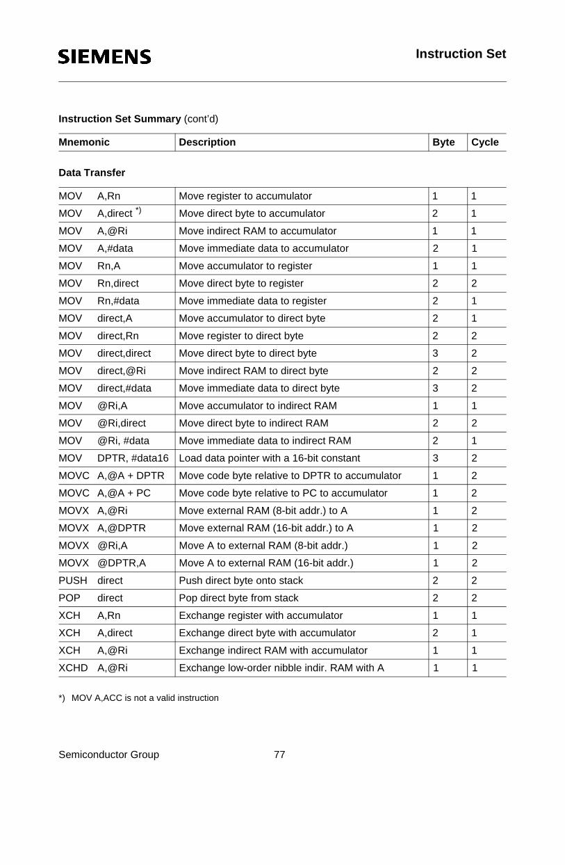
Instruction Set
Instruction Set Summary (cont’d)
Data Transfer
Mnemonic Description Byte Cycle
MOV A,Rn Move register to accumulator 1 1
MOV A,direct *) Move direct byte to accumulator 2 1
MOV A,@Ri Move indirect RAM to accumulator 1 1
Semiconductor Group 77
*) MOV A,ACC is not a valid instruction
MOV A,#data Move immediate data to accumulator 2 1
MOV Rn,A Move accumulator to register 1 1
MOV Rn,direct Move direct byte to register 2 2
MOV Rn,#data Move immediate data to register 2 1
MOV direct,A Move accumulator to direct byte 2 1
MOV direct,Rn Move register to direct byte 2 2
MOV direct,direct Move direct byte to direct byte 3 2
MOV direct,@Ri Move indirect RAM to direct byte 2 2
MOV direct,#data Move immediate data to direct byte 3 2
MOV @Ri,A Move accumulator to indirect RAM 1 1
MOV @Ri,direct Move direct byte to indirect RAM 2 2
MOV @Ri, #data Move immediate data to indirect RAM 2 1
MOV DPTR, #data16 Load data pointer with a 16-bit constant 3 2
MOVC A,@A + DPTR Move code byte relative to DPTR to accumulator 1 2
MOVC A,@A + PC Move code byte relative to PC to accumulator 1 2
MOVX A,@Ri Move external RAM (8-bit addr.) to A 1 2
MOVX A,@DPTR Move external RAM (16-bit addr.) to A 1 2
MOVX @Ri,A Move A to external RAM (8-bit addr.) 1 2
MOVX @DPTR,A Move A to external RAM (16-bit addr.) 1 2
PUSH direct Push direct byte onto stack 2 2
POP direct Pop direct byte from stack 2 2
XCH A,Rn Exchange register with accumulator 1 1
XCH A,direct Exchange direct byte with accumulator 2 1
XCH A,@Ri Exchange indirect RAM with accumulator 1 1
XCHD A,@Ri Exchange low-order nibble indir. RAM with A 1 1
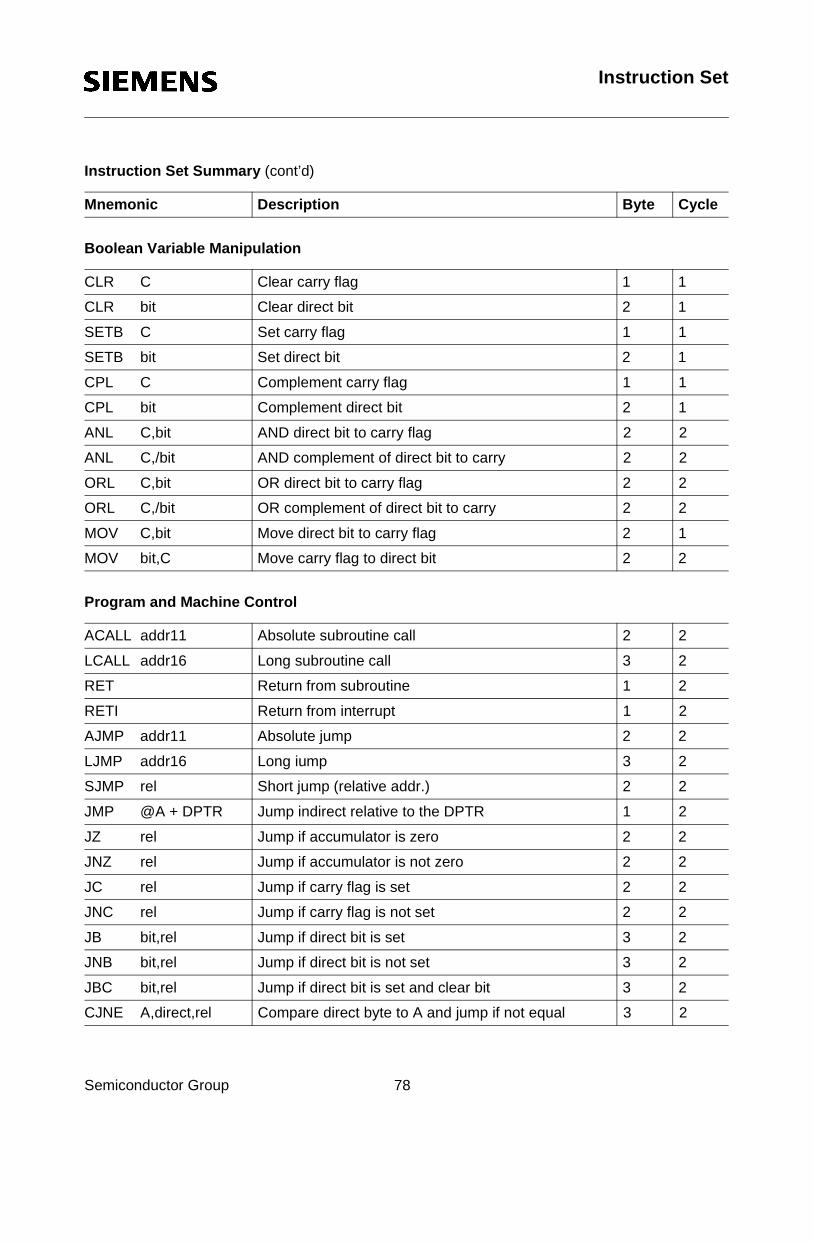
Instruction Set
Instruction Set Summary (cont’d)
Boolean Variable Manipulation
Mnemonic Description Byte Cycle
CLR C Clear carry flag 1 1
CLR bit Clear direct bit 2 1
SETB C Set carry flag 1 1
Semiconductor Group 78
Program and Machine Control
SETB bit Set direct bit 2 1
CPL C Complement carry flag 1 1
CPL bit Complement direct bit 2 1
ANL C,bit AND direct bit to carry flag 2 2
ANL C,/bit AND complement of direct bit to carry 2 2
ORL C,bit OR direct bit to carry flag 2 2
ORL C,/bit OR complement of direct bit to carry 2 2
MOV C,bit Move direct bit to carry flag 2 1
MOV bit,C Move carry flag to direct bit 2 2
ACALL addr11 Absolute subroutine call 2 2
LCALL addr16 Long subroutine call 3 2
RET Return from subroutine 1 2
RETI Return from interrupt 1 2
AJMP addr11 Absolute jump 2 2
LJMP addr16 Long iump 3 2
SJMP rel Short jump (relative addr.) 2 2
JMP @A + DPTR Jump indirect relative to the DPTR 1 2
JZ rel Jump if accumulator is zero 2 2
JNZ rel Jump if accumulator is not zero 2 2
JC rel Jump if carry flag is set 2 2
JNC rel Jump if carry flag is not set 2 2
JB bit,rel Jump if direct bit is set 3 2
JNB bit,rel Jump if direct bit is not set 3 2
JBC bit,rel Jump if direct bit is set and clear bit 3 2
CJNE A,direct,rel Compare direct byte to A and jump if not equal 3 2
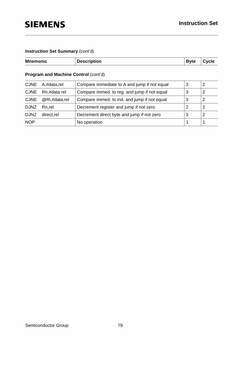
Instruction Set
Instruction Set Summary (cont’d)
Program and Machine Control (cont’d)
Mnemonic Description Byte Cycle
CJNE A,#data,rel Compare immediate to A and jump if not equal 3 2
CJNE Rn,#data rel Compare immed. to reg. and jump if not equal 3 2
CJNE @Ri,#data,rel Compare immed. to ind. and jump if not equal 3 2
Semiconductor Group 79
DJNZ Rn,rel Decrement register and jump if not zero 2 2
DJNZ direct,rel Decrement direct byte and jump if not zero 3 2
NOP No operation 1 1