perspective in photovoltaics
148
Solar Cells – a perspective Vikram Kumar Nanoscale Research Facility Indian Institute of T echnology New Delhi [email protected]
-
Upload
vkmr477186 -
Category
Documents
-
view
236 -
download
0
Transcript of perspective in photovoltaics
7/29/2019 perspective in photovoltaics
http://slidepdf.com/reader/full/perspective-in-photovoltaics 1/148
Solar Cells – a perspective
Vikram Kumar Nanoscale Research FacilityIndian Institute of Technology
7/29/2019 perspective in photovoltaics
http://slidepdf.com/reader/full/perspective-in-photovoltaics 2/148
0902022
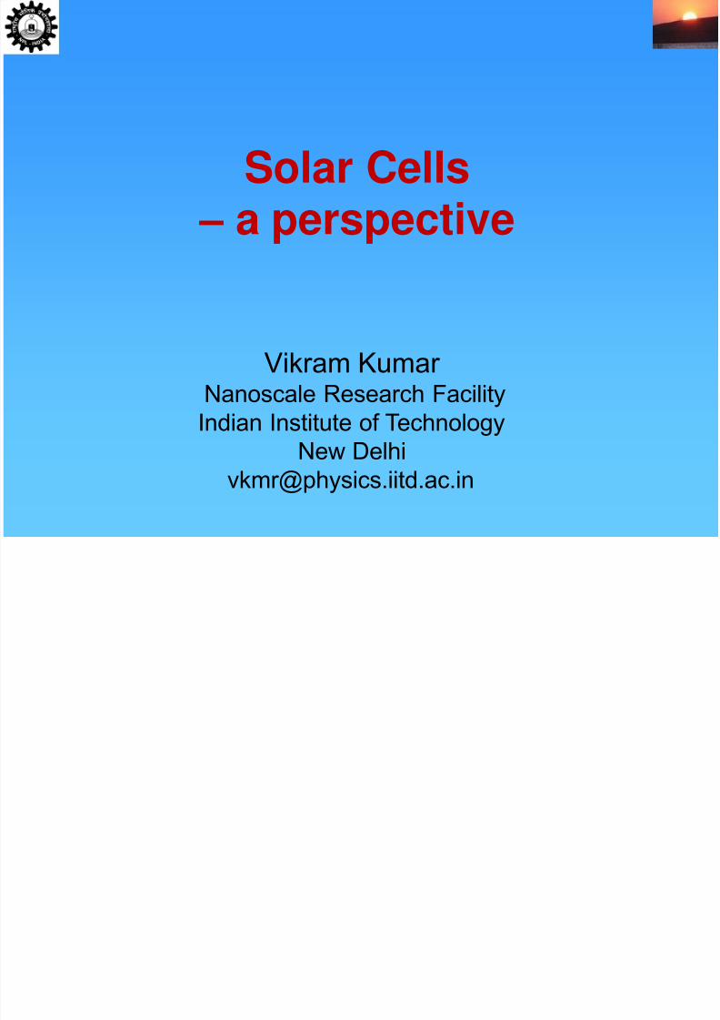
National PhysicalLaboratory
NPL is the custodian of National Standards of Measurements in India
7/29/2019 perspective in photovoltaics
http://slidepdf.com/reader/full/perspective-in-photovoltaics 3/148
0902023
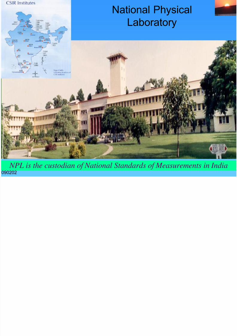
R&D Divisions of NPLPhysico-Mechanical
Standards
Electrical & Electronic
Standards
NPLRadio &
Atmospheric
Sciences
Cryogenics &
Superconductivity
Engineering
Materials
Electronic
Materials
MaterialsCharacterization
library, computing facilities,
internet, workshop,
glassblowing, electronicinstrumentation etc.
Employees – 854
Scientists – 197
Temp Scientists – 212
Budget: ~ 20 M$
Papers in 2008 – 259
7/29/2019 perspective in photovoltaics
http://slidepdf.com/reader/full/perspective-in-photovoltaics 4/148
090202 4
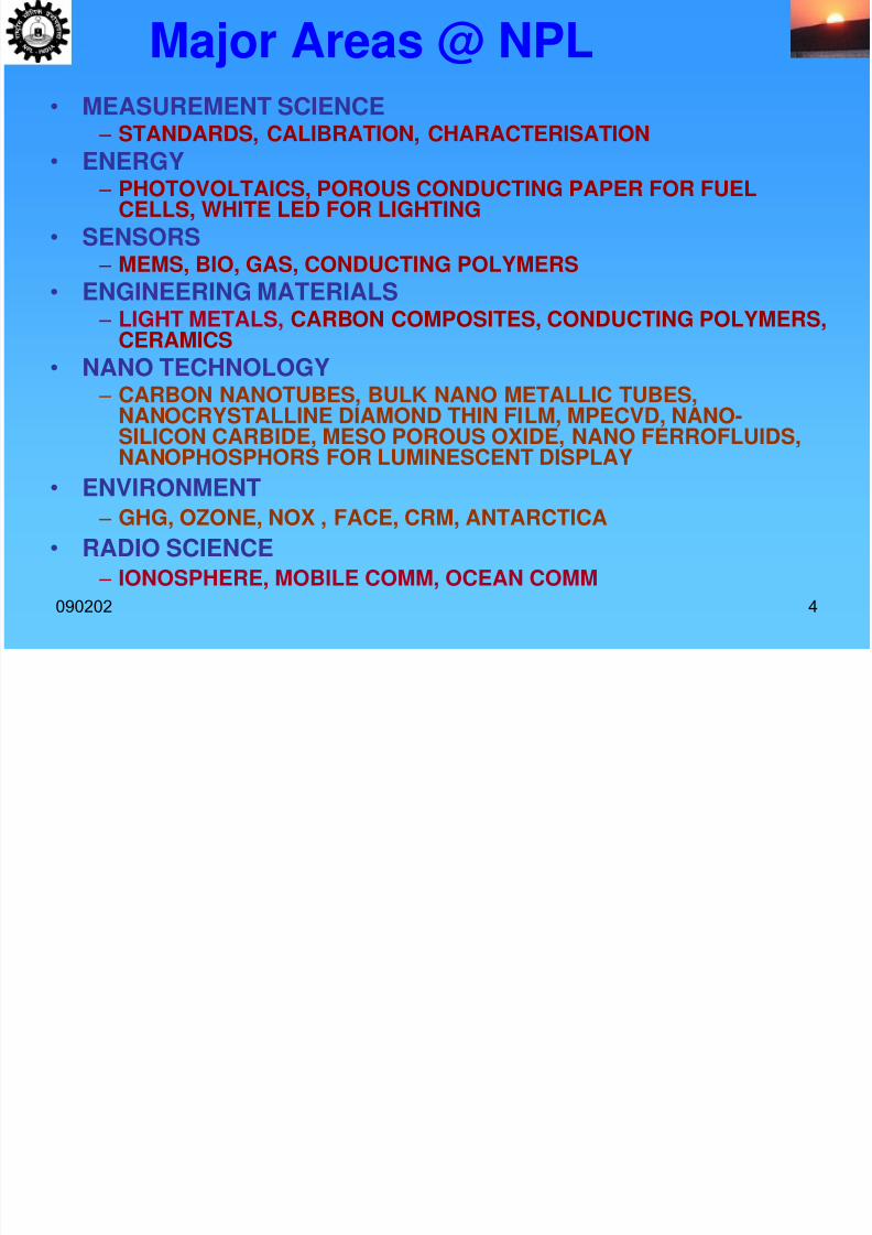
Major Areas @ NPL• MEASUREMENT SCIENCE
– STANDARDS, CALIBRATION, CHARACTERISATION
• ENERGY – PHOTOVOLTAICS, POROUS CONDUCTING PAPER FOR FUEL
CELLS, WHITE LED FOR LIGHTING
• SENSORS – MEMS, BIO, GAS, CONDUCTING POLYMERS
• ENGINEERING MATERIALS – LIGHT METALS, CARBON COMPOSITES, CONDUCTING POLYMERS,CERAMICS
• NANO TECHNOLOGY – CARBON NANOTUBES, BULK NANO METALLIC TUBES,
NANOCRYSTALLINE DIAMOND THIN FILM, MPECVD, NANO-SILICON CARBIDE, MESO POROUS OXIDE, NANO FERROFLUIDS,
NANOPHOSPHORS FOR LUMINESCENT DISPLAY• ENVIRONMENT
– GHG, OZONE, NOX , FACE, CRM, ANTARCTICA
• RADIO SCIENCE – IONOSPHERE, MOBILE COMM, OCEAN COMM
7/29/2019 perspective in photovoltaics
http://slidepdf.com/reader/full/perspective-in-photovoltaics 5/148
080523 6
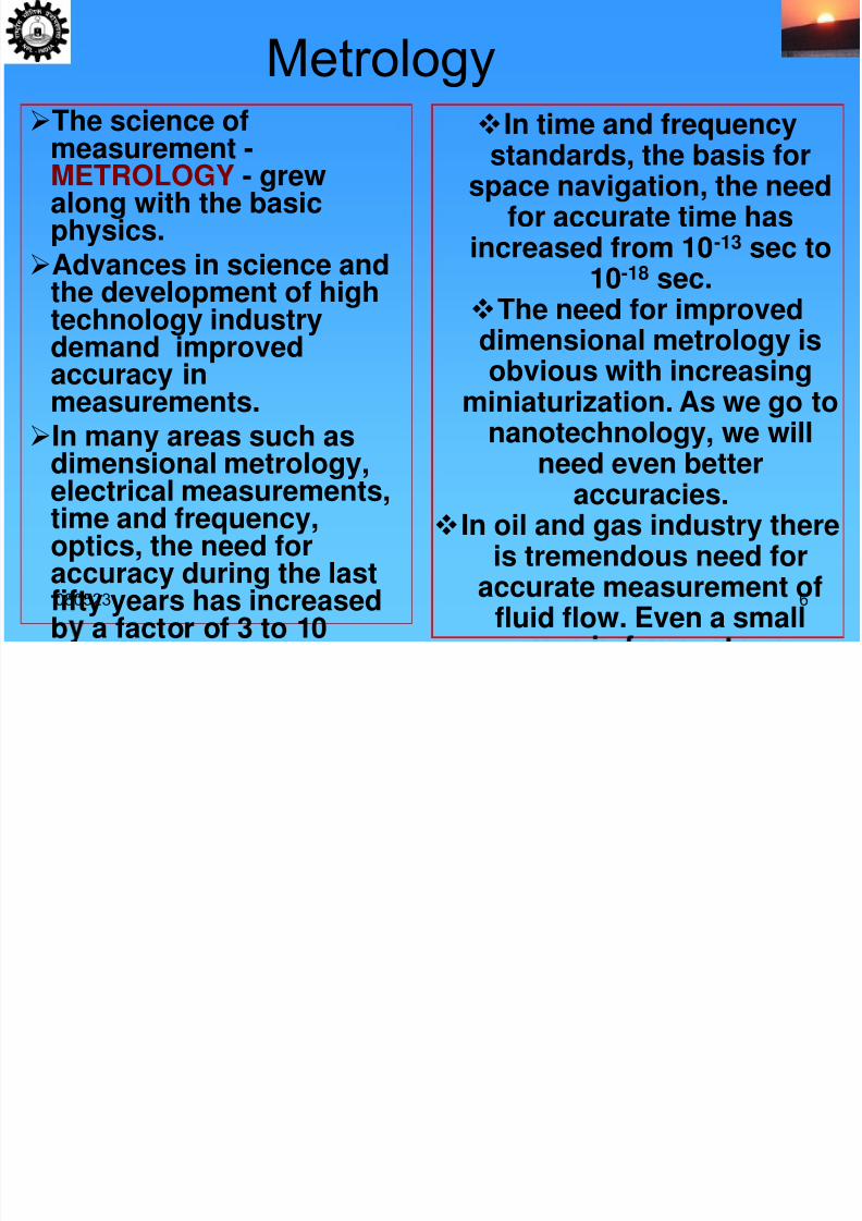
MetrologyThe science of
measurement -METROLOGY - grewalong with the basicphysics.
Advances in science and
the development of hightechnology industrydemand improvedaccuracy inmeasurements.
In many areas such asdimensional metrology,electrical measurements,time and frequency,optics, the need foraccuracy during the last
fifty years has increasedb a factor of 3 to 10
In time and frequency
standards, the basis forspace navigation, the need
for accurate time hasincreased from 10-13 sec to
10-18 sec.The need for improveddimensional metrology isobvious with increasing
miniaturization. As we go tonanotechnology, we will
need even betteraccuracies.
In oil and gas industry thereis tremendous need for
accurate measurement offluid flow. Even a small
7/29/2019 perspective in photovoltaics
http://slidepdf.com/reader/full/perspective-in-photovoltaics 6/148
080523 7
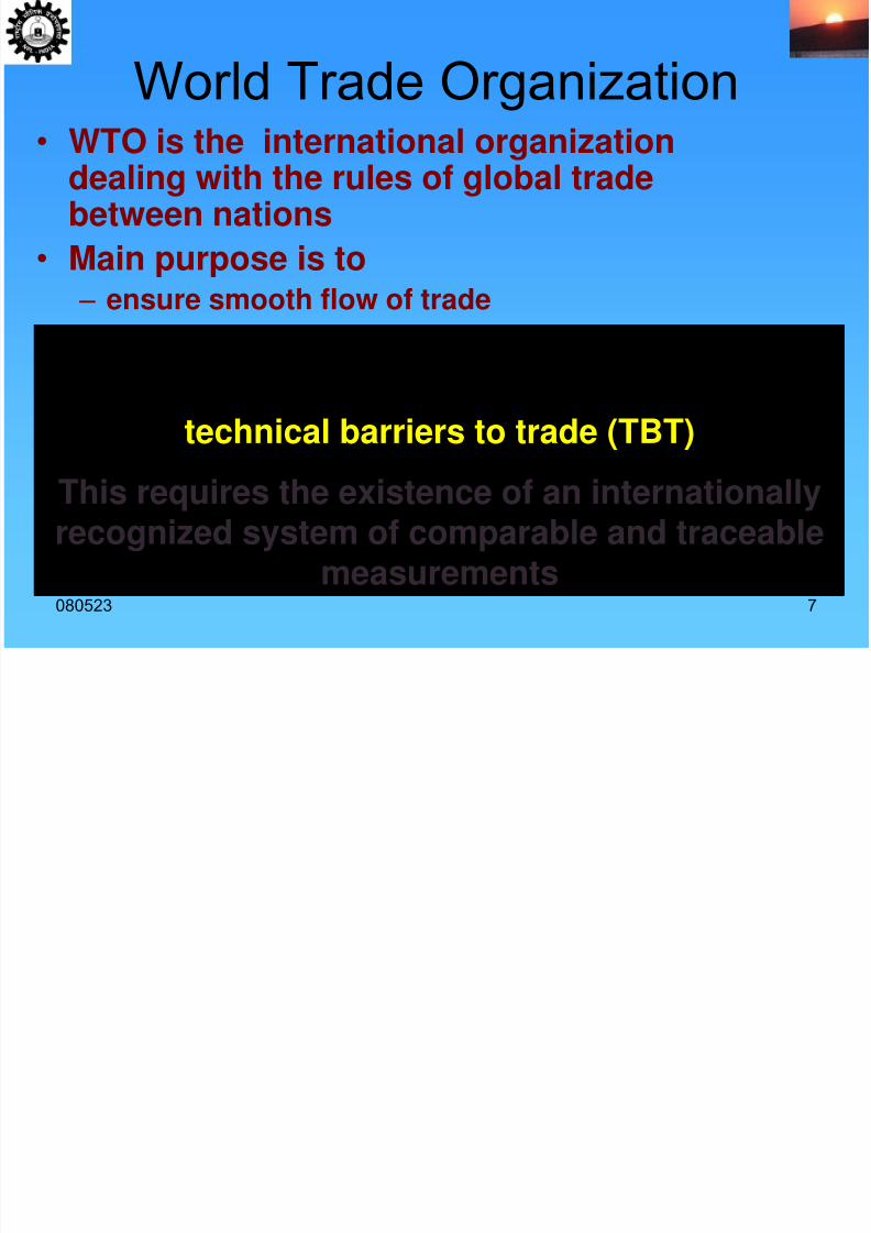
World Trade Organization
• WTO is the international organizationdealing with the rules of global tradebetween nations
• Main purpose is to
– ensure smooth flow of trade – predictable and as free as possible
As part of WTO agreement all signatory nationsare committed to remove all barriers including
technical barriers to trade (TBT)
This requires the existence of an internationallyrecognized system of comparable and traceable
measurements
7/29/2019 perspective in photovoltaics
http://slidepdf.com/reader/full/perspective-in-photovoltaics 7/148
080523 8
7/29/2019 perspective in photovoltaics
http://slidepdf.com/reader/full/perspective-in-photovoltaics 8/148
080523 9
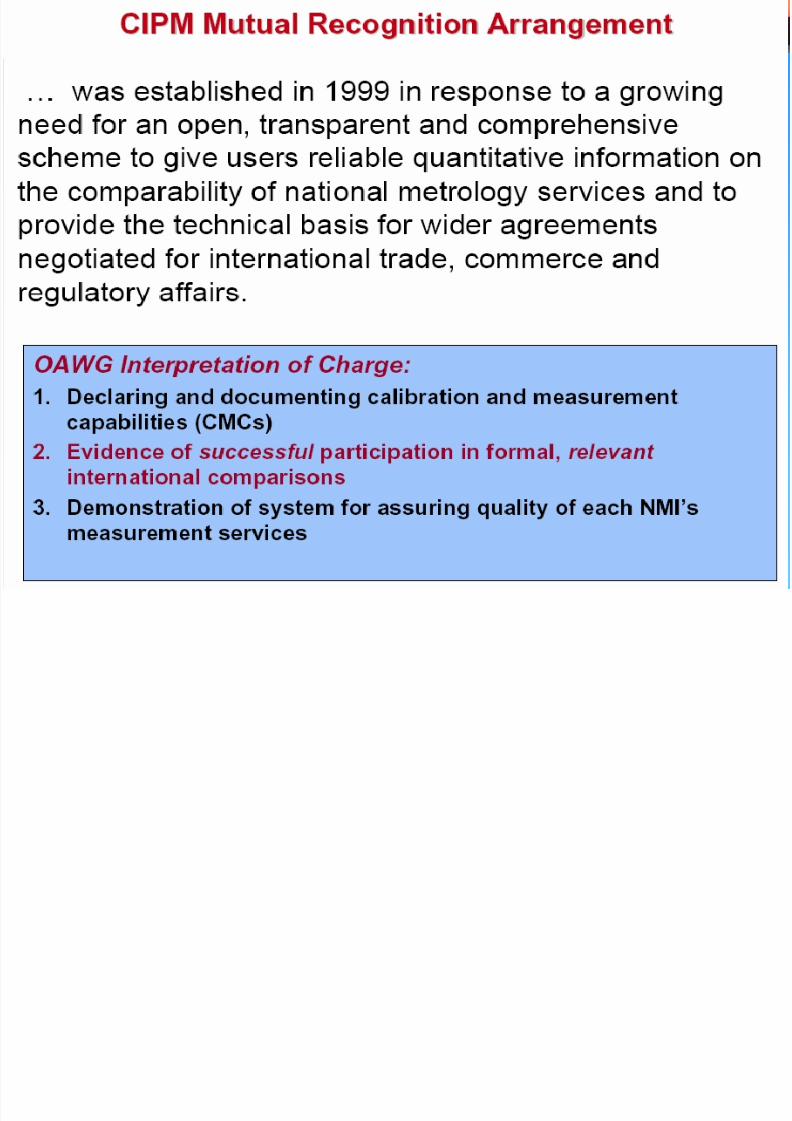
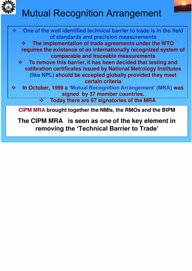
Mutual Recognition Arrangement
One of the well identified technical barrier to trade is in the fieldof standards and precision measurements The implementation of trade agreements under the WTOrequires the existence of an internationally recognized system of
comparable and traceable measurements To remove this barrier, it has been decided that testing and
calibration certificates issued by National Metrology Institutes(like NPL) should be accepted globally provided they meet
certain criteria In October, 1999 a „Mutual Recognition Arrangement‟ (MRA) was
signed by 37 member countries.
Today there are 67 signatories of the MRA
CIPM MRA brought together the NMIs, the RMOs and the BIPM
The CIPM MRA is seen as one of the key element inremoving the „Technical Barrier to Trade‟
7/29/2019 perspective in photovoltaics
http://slidepdf.com/reader/full/perspective-in-photovoltaics 9/148
sspl/nsd
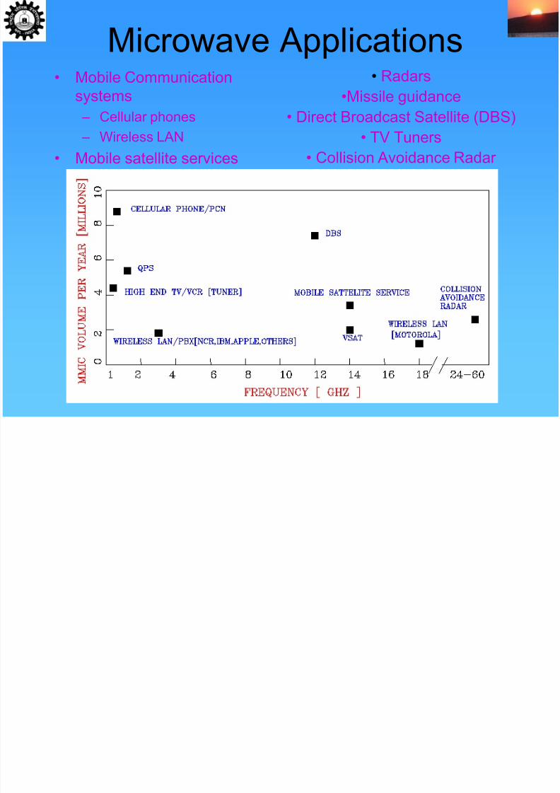
Microwave Applications• Mobile Communication
systems – Cellular phones
– Wireless LAN
• Mobile satellite services
• Radars
•Missile guidance• Direct Broadcast Satellite (DBS)
• TV Tuners
• Collision Avoidance Radar
7/29/2019 perspective in photovoltaics
http://slidepdf.com/reader/full/perspective-in-photovoltaics 10/148
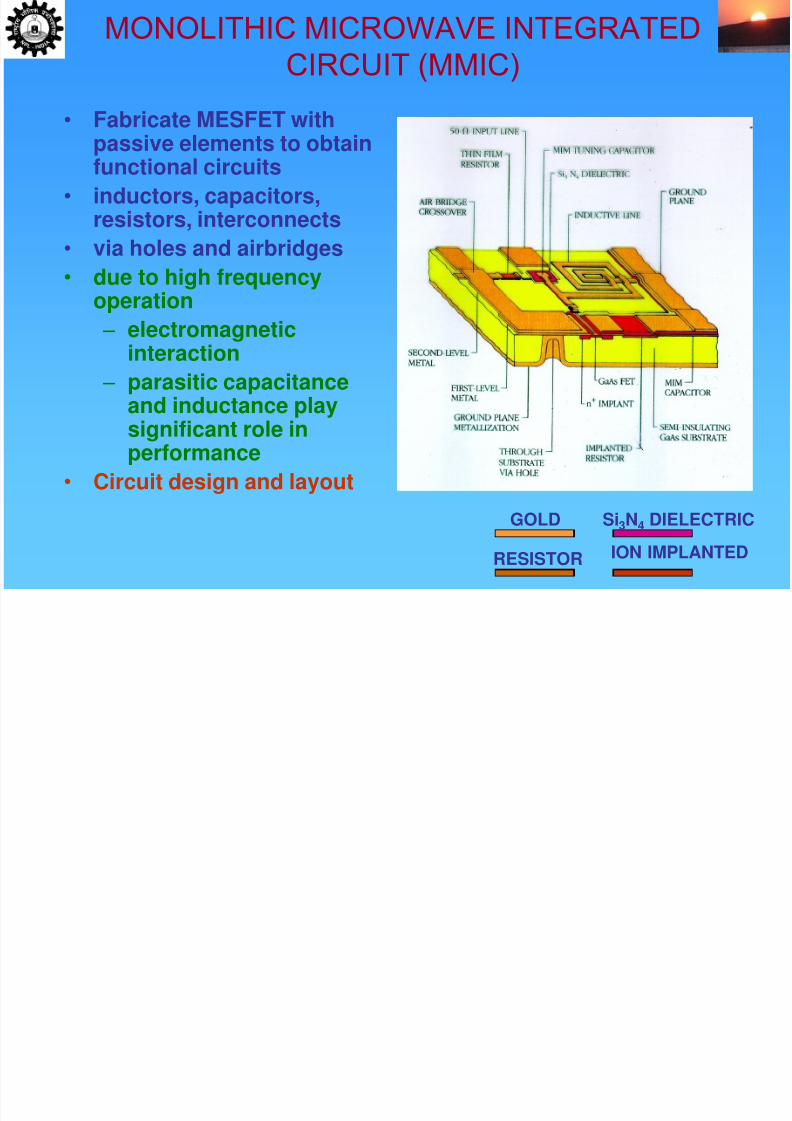
MONOLITHIC MICROWAVE INTEGRATEDCIRCUIT (MMIC)
GOLD Si3N4 DIELECTRIC
RESISTOR ION IMPLANTED
• Fabricate MESFET with
passive elements to obtainfunctional circuits
• inductors, capacitors,resistors, interconnects
• via holes and airbridges
• due to high frequencyoperation
– electromagneticinteraction
– parasitic capacitance
and inductance playsignificant role inperformance
• Circuit design and layout
7/29/2019 perspective in photovoltaics
http://slidepdf.com/reader/full/perspective-in-photovoltaics 11/148
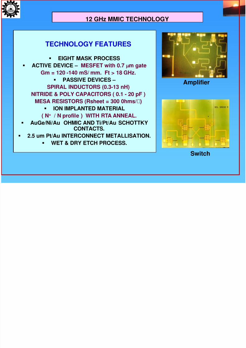
12 GHz MMIC TECHNOLOGY
TECHNOLOGY FEATURES
EIGHT MASK PROCESS
ACTIVE DEVICE – MESFET with 0.7 m gate
Gm = 120 -140 mS/ mm. Ft > 18 GHz.
PASSIVE DEVICES –
SPIRAL INDUCTORS (0.3-13 nH)NITRIDE & POLY CAPACITORS ( 0.1 - 20 pF )
MESA RESISTORS (Rsheet = 300 0hms/ )
ION IMPLANTED MATERIAL
( N+ / N profile ) WITH RTA ANNEAL.
AuGe/Ni/Au OHMIC AND Ti/Pt/Au SCHOTTKY
CONTACTS. 2.5 um Pt/Au INTERCONNECT METALLISATION.
WET & DRY ETCH PROCESS.
Amplifier
Switch
7/29/2019 perspective in photovoltaics
http://slidepdf.com/reader/full/perspective-in-photovoltaics 12/148
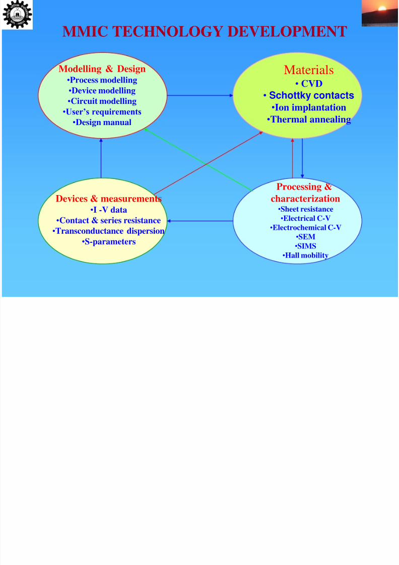
Modelling & Design •Process modelling
•Device modelling
•Circuit modelling
•User’s requirements
•Design manual
Materials • CVD
• Schottky contacts
•Ion implantation
•Thermal annealing
Devices & measurements
•I -V data•Contact & series resistance
•Transconductance dispersion
•S-parameters
Processing &
characterization
•Sheet resistance•Electrical C-V
•Electrochemical C-V•SEM•SIMS
•Hall mobility
MMIC TECHNOLOGY DEVELOPMENT
7/29/2019 perspective in photovoltaics
http://slidepdf.com/reader/full/perspective-in-photovoltaics 13/148
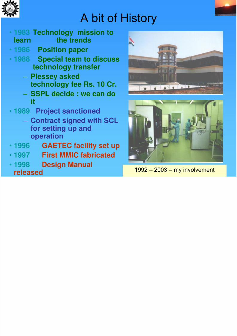
A bit of History• 1983 Technology mission to
learn the trends• 1986 Position paper
• 1988 Special team to discusstechnology transfer
– Plessey asked
technology fee Rs. 10 Cr. – SSPL decide : we can do
it
• 1989 Project sanctioned
– Contract signed with SCLfor setting up andoperation
• 1996 GAETEC facility set up
• 1997 First MMIC fabricated
• 1998 Design Manualreleased 1992 – 2003 – my involvement
7/29/2019 perspective in photovoltaics
http://slidepdf.com/reader/full/perspective-in-photovoltaics 14/148
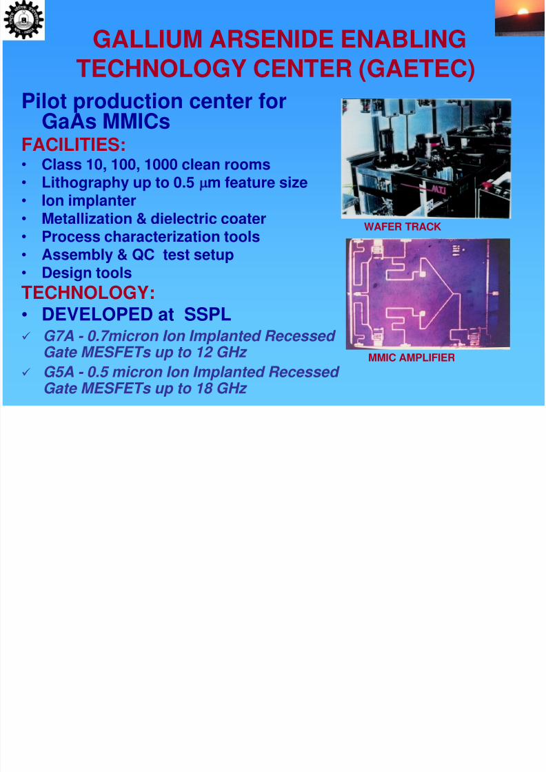
GALLIUM ARSENIDE ENABLINGTECHNOLOGY CENTER (GAETEC)
Pilot production center forGaAs MMICs
FACILITIES: • Class 10, 100, 1000 clean rooms• Lithography up to 0.5 m feature size• Ion implanter• Metallization & dielectric coater• Process characterization tools• Assembly & QC test setup• Design tools
TECHNOLOGY:• DEVELOPED at SSPL G7A - 0.7micron Ion Implanted Recessed
Gate MESFETs up to 12 GHz
G5A - 0.5 micron Ion Implanted Recessed Gate MESFETs up to 18 GHz
WAFER TRACK
MMIC AMPLIFIER

7/29/2019 perspective in photovoltaics
http://slidepdf.com/reader/full/perspective-in-photovoltaics 15/148
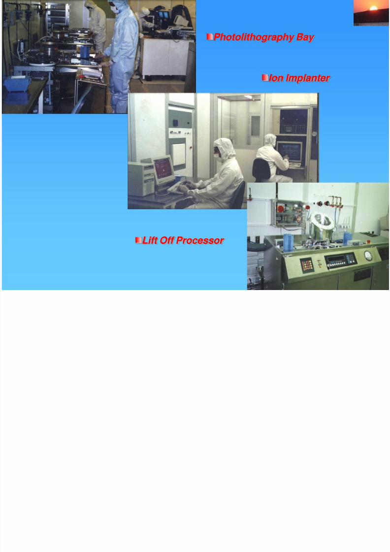
GAETEC Has a Modern Wafer Fabrication Facility with Class 10, Class 100 Cleanrooms Housing
State- Of- Art Equipment
GAETEC FOUNDRY
7/29/2019 perspective in photovoltaics
http://slidepdf.com/reader/full/perspective-in-photovoltaics 16/148
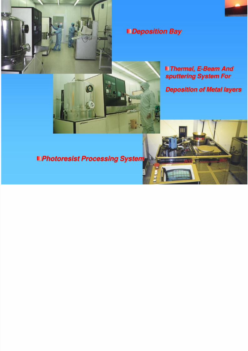
Lift Off Processor
Photolithography Bay
Ion Implanter
7/29/2019 perspective in photovoltaics
http://slidepdf.com/reader/full/perspective-in-photovoltaics 17/148
Thermal, E-Beam And sputtering System For
Deposition of Metal layers
Deposition Bay
Photoresist Processing System
7/29/2019 perspective in photovoltaics
http://slidepdf.com/reader/full/perspective-in-photovoltaics 18/148
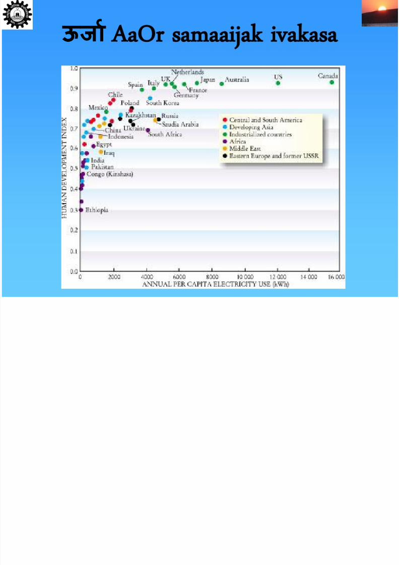
ऊरजा
7/29/2019 perspective in photovoltaics
http://slidepdf.com/reader/full/perspective-in-photovoltaics 19/148
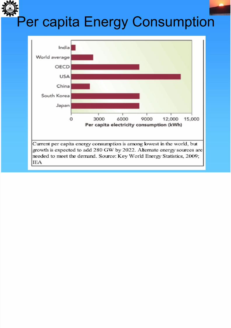
Per capita Energy Consumption
7/29/2019 perspective in photovoltaics
http://slidepdf.com/reader/full/perspective-in-photovoltaics 20/148
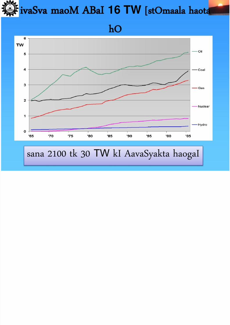
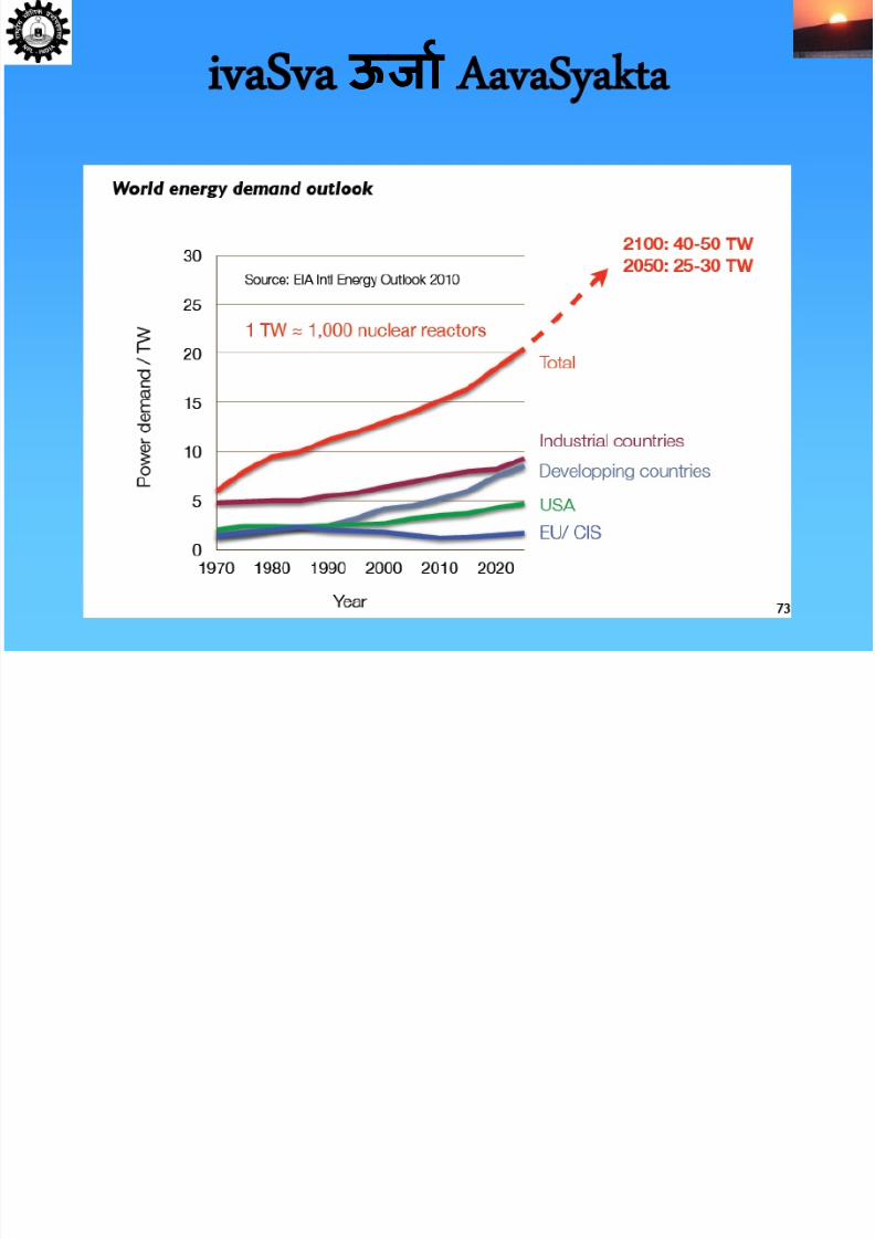
16 TW
sana 2100 tk 30 TW kI AavaSyakta haogaI
7/29/2019 perspective in photovoltaics
http://slidepdf.com/reader/full/perspective-in-photovoltaics 21/148
23
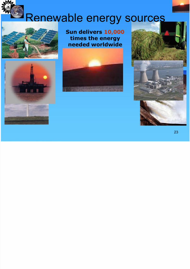
Renewable energy sources
Sun delivers 10,000times the energyneeded worldwide
7/29/2019 perspective in photovoltaics
http://slidepdf.com/reader/full/perspective-in-photovoltaics 22/148
090723 24
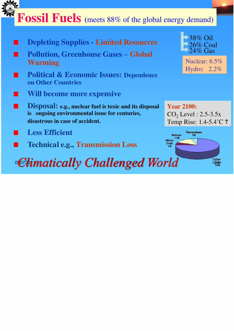
Depleting Supplies - Limited ResourcesPollution, Greenhouse Gases – GlobalWarming
Political & Economic Issues: Dependence
on Other Countries
Will become more expensive
Disposal: e.g., nuclear fuel is toxic and its disposalis ongoing environmental issue for centuries,
disastrous in case of accident. Less Efficient
Technical e.g., Transmission Loss
Year 2100:CO2 Level : 2.5-3.5x
Temp Rise: 1.4-5.4˚C
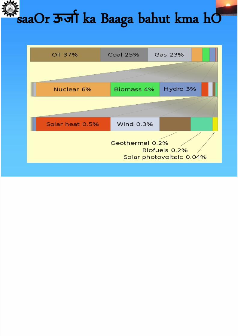
Fossil Fuels (meets 88% of the global energy demand)
38% Oil26% Coal24% Gas
Nuclear: 6.5%
Hydro: 2.2%
Climatically Challenged World
ा ा
7/29/2019 perspective in photovoltaics
http://slidepdf.com/reader/full/perspective-in-photovoltaics 23/148
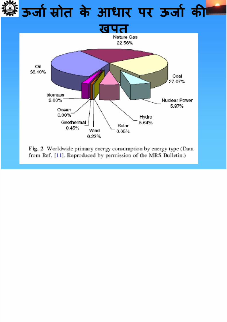
ऊरजा ोत के आधज ऩ ऊरजा क खऩत
7/29/2019 perspective in photovoltaics
http://slidepdf.com/reader/full/perspective-in-photovoltaics 24/148
090723 26
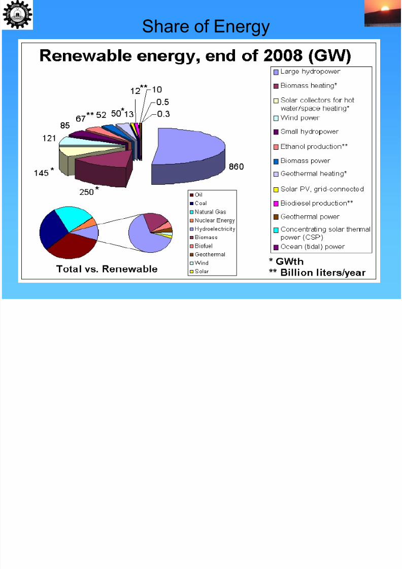
Share of Energy
7/29/2019 perspective in photovoltaics
http://slidepdf.com/reader/full/perspective-in-photovoltaics 25/148
ऊरजा
7/29/2019 perspective in photovoltaics
http://slidepdf.com/reader/full/perspective-in-photovoltaics 26/148
090723 28
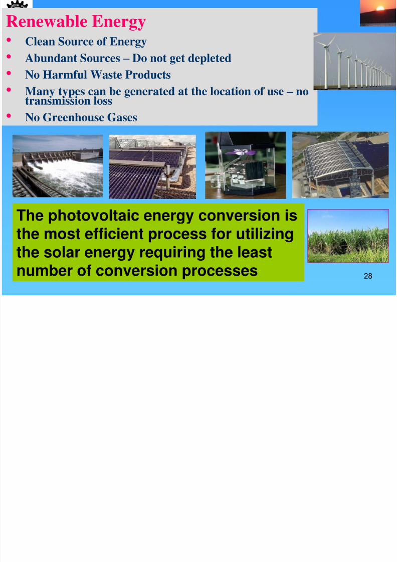
Renewable Energy • Clean Source of Energy
• Abundant Sources – Do not get depleted
• No Harmful Waste Products
• Many types can be generated at the location of use – notransmission loss
• No Greenhouse Gases
The photovoltaic energy conversion isthe most efficient process for utilizingthe solar energy requiring the least
number of conversion processes
7/29/2019 perspective in photovoltaics
http://slidepdf.com/reader/full/perspective-in-photovoltaics 27/148
090723 29
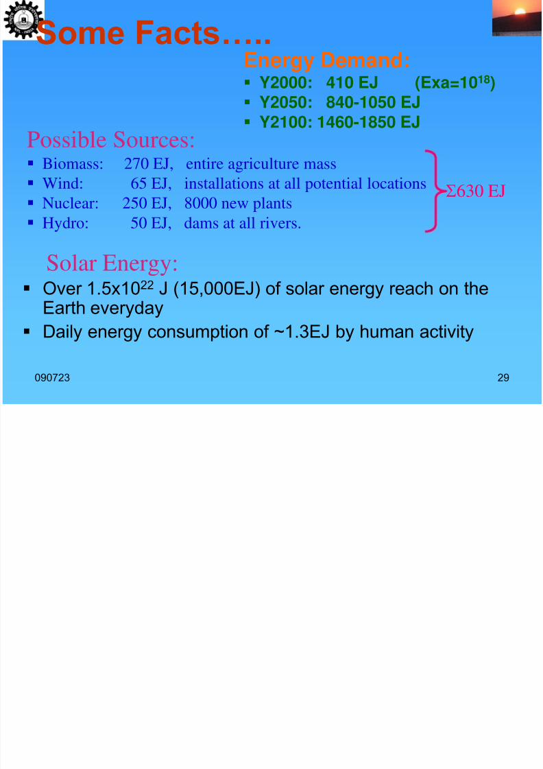
Some Facts….. Energy Demand: Y2000: 410 EJ (Exa=1018)
Y2050: 840-1050 EJ Y2100: 1460-1850 EJ
Possible Sources: Biomass: 270 EJ, entire agriculture mass
Wind: 65 EJ, installations at all potential locations
Nuclear: 250 EJ, 8000 new plants
Hydro: 50 EJ, dams at all rivers.
630 EJ
Over 1.5x10²² J (15,000EJ) of solar energy reach on theEarth everyday
Daily energy consumption of ~1.3EJ by human activity
Solar Energy:
7/29/2019 perspective in photovoltaics
http://slidepdf.com/reader/full/perspective-in-photovoltaics 28/148
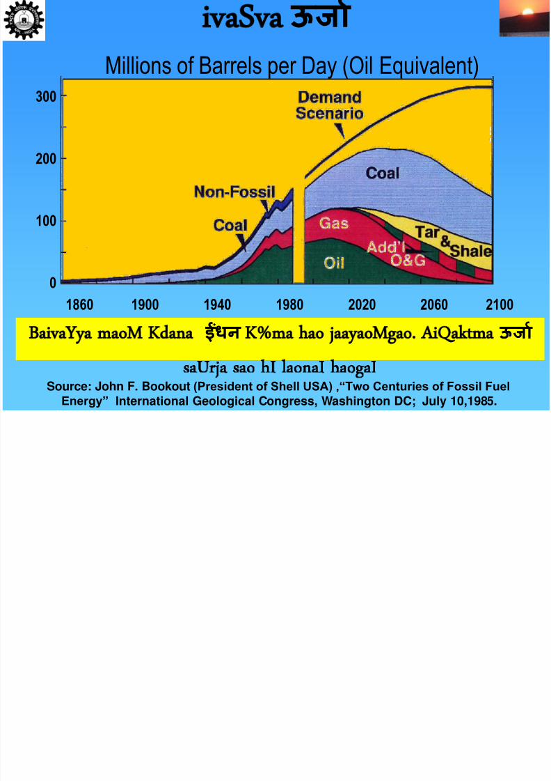
ऊरज Millions of Barrels per Day (Oil Equivalent)
300
200
100
0
1860 1900 1940 1980 2020 2060 2100
Source: John F. Bookout (President of Shell USA) ,“Two Centuries of Fossil FuelEnergy” International Geological Congress, Washington DC; July 10,1985.
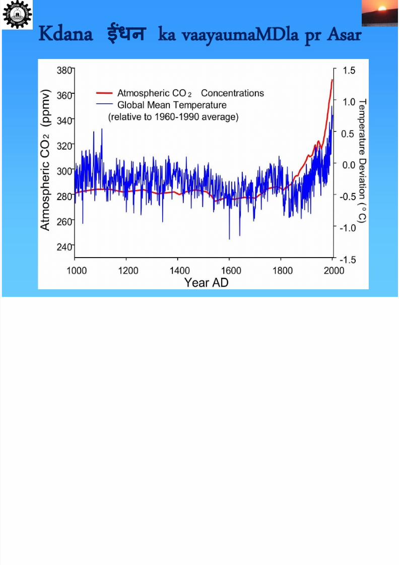
ईधन ऊरजा
7/29/2019 perspective in photovoltaics
http://slidepdf.com/reader/full/perspective-in-photovoltaics 29/148
090723 31
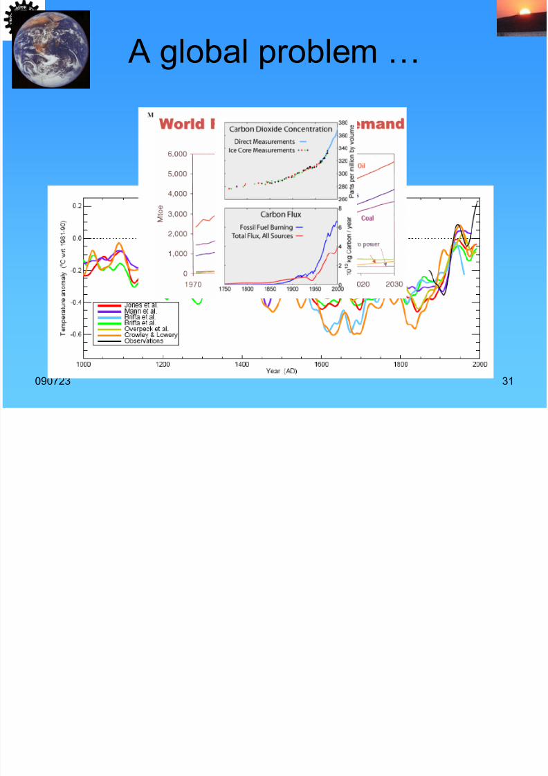
A global problem …
7/29/2019 perspective in photovoltaics
http://slidepdf.com/reader/full/perspective-in-photovoltaics 30/148
ईधन
7/29/2019 perspective in photovoltaics
http://slidepdf.com/reader/full/perspective-in-photovoltaics 31/148
ऊरजा

7/29/2019 perspective in photovoltaics
http://slidepdf.com/reader/full/perspective-in-photovoltaics 32/148
• ेऱ भॊडा वतमान खप द प 43 साऱ
• वतमान खप द प गैस के
भॊडा 64
साऱ • वतमान खप द प कोयऱा भॊडा 312 वष म
• पमाण ु ऊरात
7/29/2019 perspective in photovoltaics
http://slidepdf.com/reader/full/perspective-in-photovoltaics 33/148
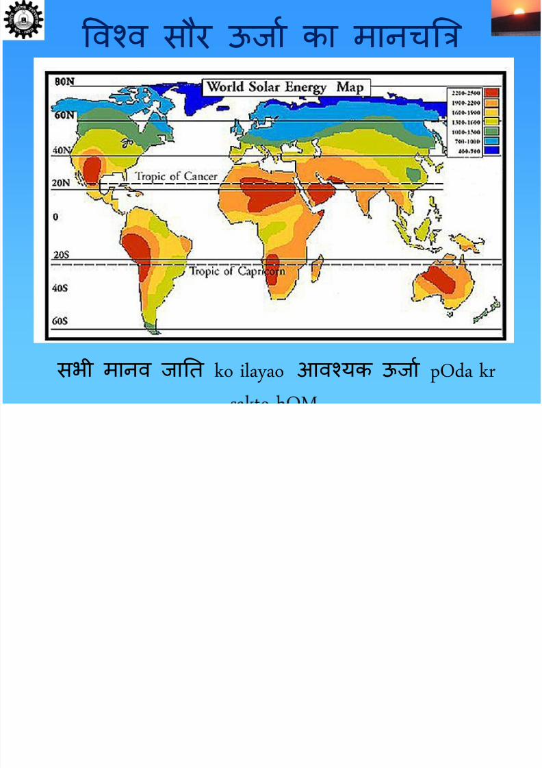
वव सौ ऊरात का मानिच
सभी मानव रा
ko ilayao
आवयक ऊरात
pOda kr
7/29/2019 perspective in photovoltaics
http://slidepdf.com/reader/full/perspective-in-photovoltaics 34/148
पेम
7/29/2019 perspective in photovoltaics
http://slidepdf.com/reader/full/perspective-in-photovoltaics 35/148
37
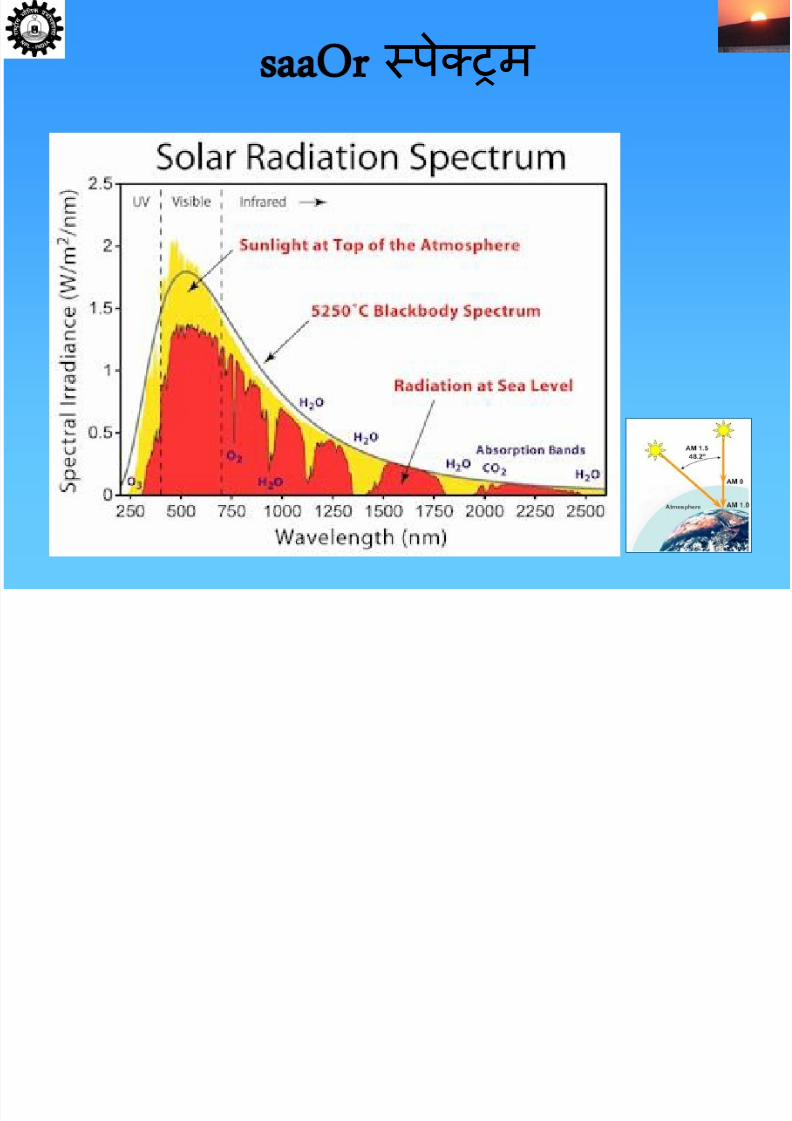
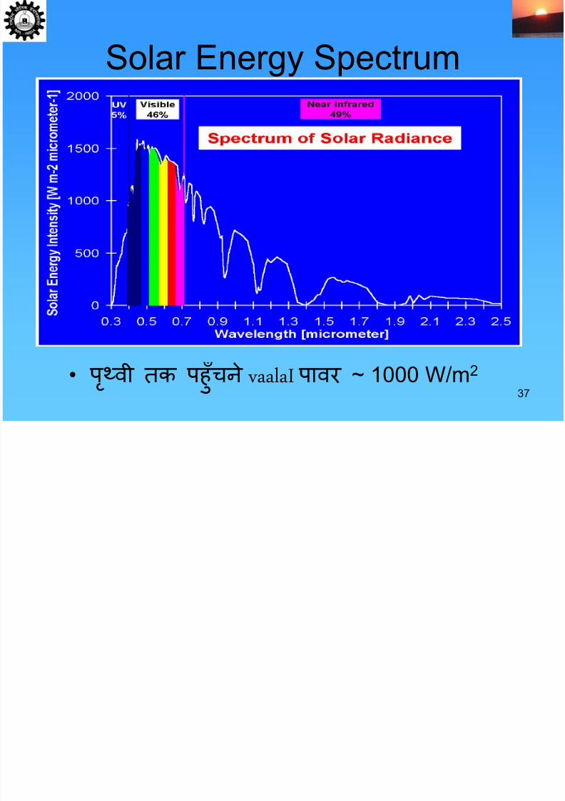
Solar Energy Spectrum
• प थृवी क पह ुिने vaalaI पाव ~ 1000 W/m2
7/29/2019 perspective in photovoltaics
http://slidepdf.com/reader/full/perspective-in-photovoltaics 36/148
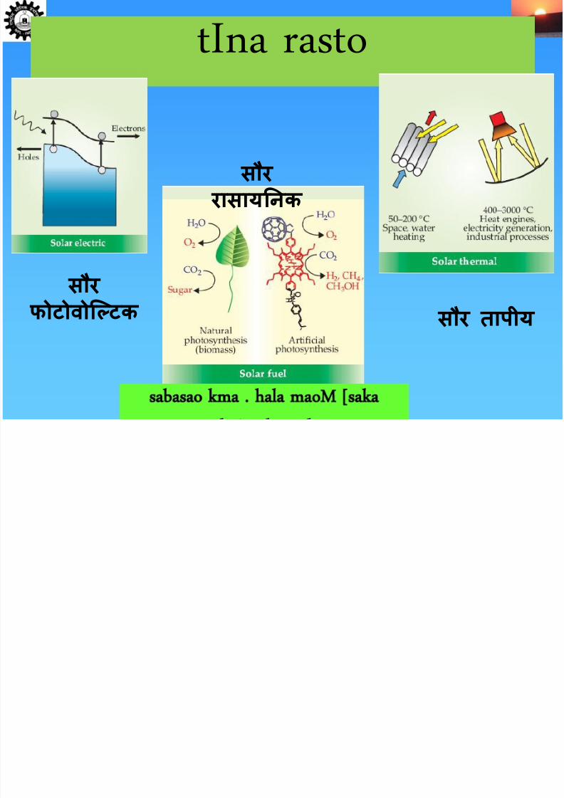
tIna rasto
सौ तजऩीय सौ पोटोवोलटक
सौ
जसजयनक
7/29/2019 perspective in photovoltaics
http://slidepdf.com/reader/full/perspective-in-photovoltaics 37/148
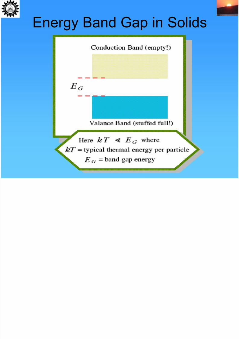
Energy Band Gap in Solids
7/29/2019 perspective in photovoltaics
http://slidepdf.com/reader/full/perspective-in-photovoltaics 38/148
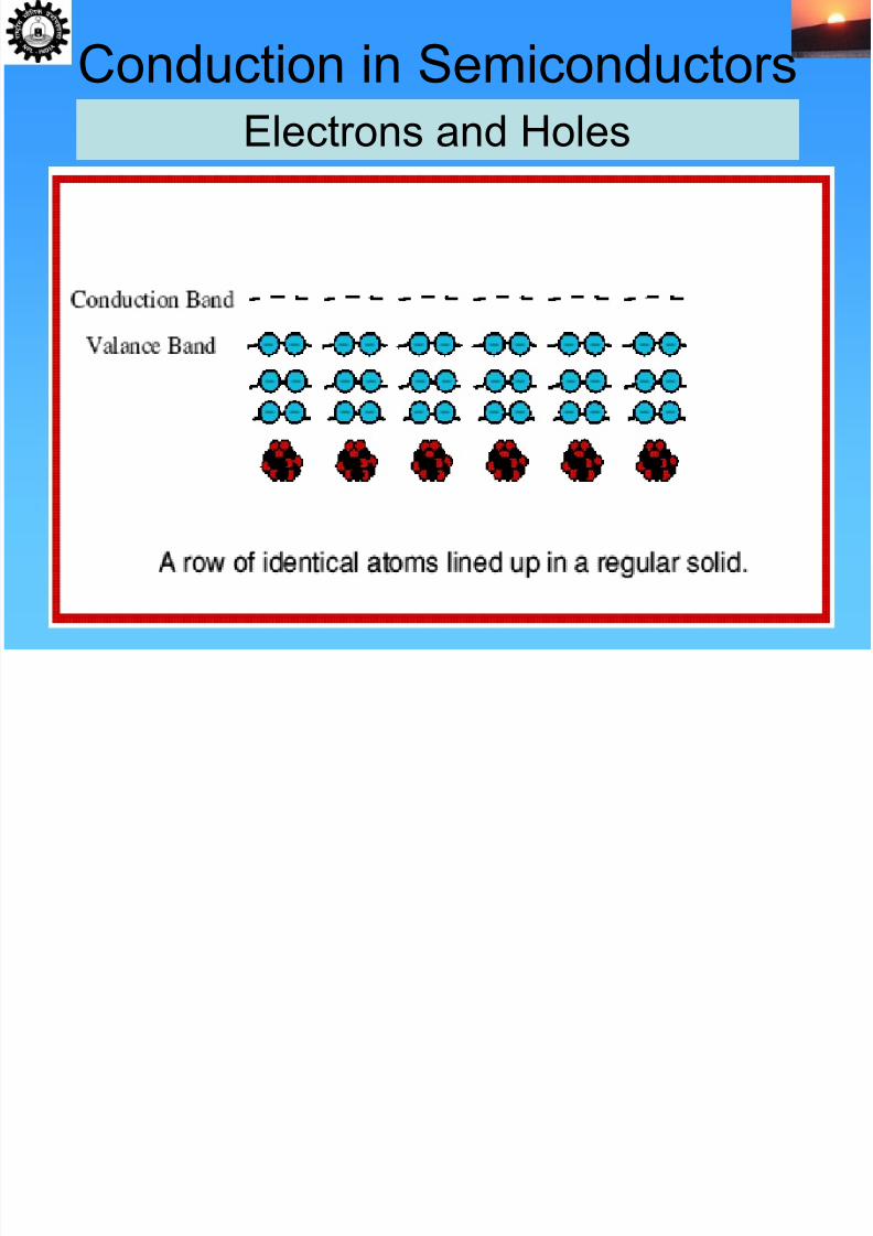
Conduction in SemiconductorsElectrons and Holes
7/29/2019 perspective in photovoltaics
http://slidepdf.com/reader/full/perspective-in-photovoltaics 39/148
7/29/2019 perspective in photovoltaics
http://slidepdf.com/reader/full/perspective-in-photovoltaics 40/148
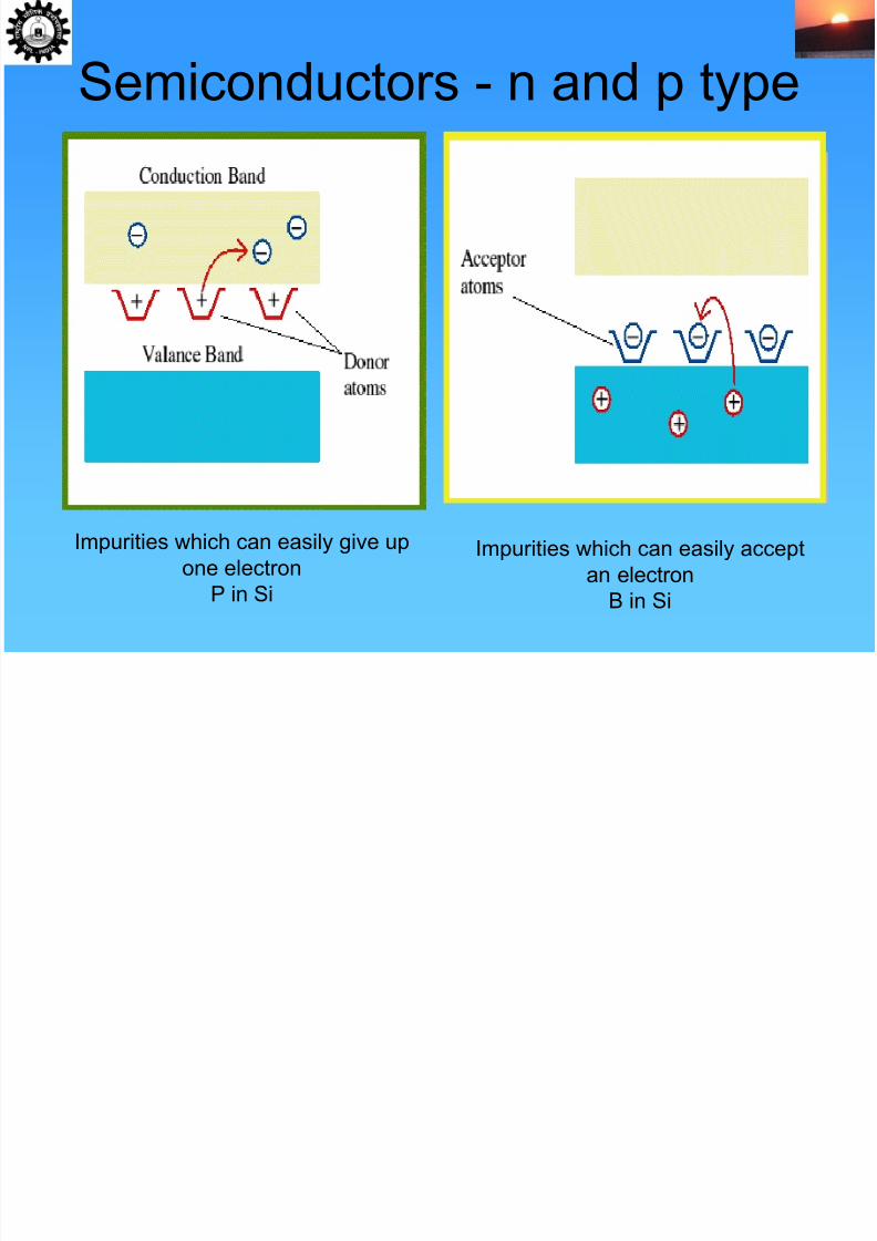
Semiconductors - n and p type
Impurities which can easily give upone electron
P in Si
Impurities which can easily acceptan electron
B in Si
त
7/29/2019 perspective in photovoltaics
http://slidepdf.com/reader/full/perspective-in-photovoltaics 41/148
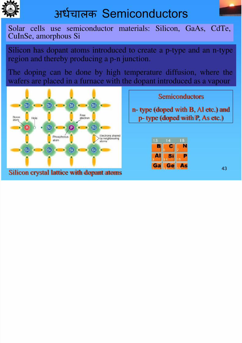
43Silicon crystal lattice with dopant atoms
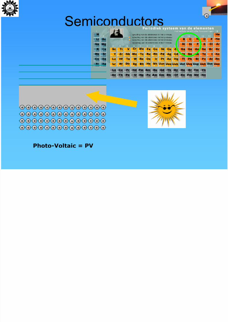
अतिाऱक SemiconductorsSolar cells use semiconductor materials: Silicon, GaAs, CdTe,CuInSe, amorphous Si
Semiconductors
n- type (doped with B, Al etc.) and
p- type (doped with P, As etc.)
Silicon has dopant atoms introduced to create a p-type and an n-typeregion and thereby producing a p-n junction.
The doping can be done by high temperature diffusion, where thewafers are placed in a furnace with the dopant introduced as a vapour
7/29/2019 perspective in photovoltaics
http://slidepdf.com/reader/full/perspective-in-photovoltaics 42/148
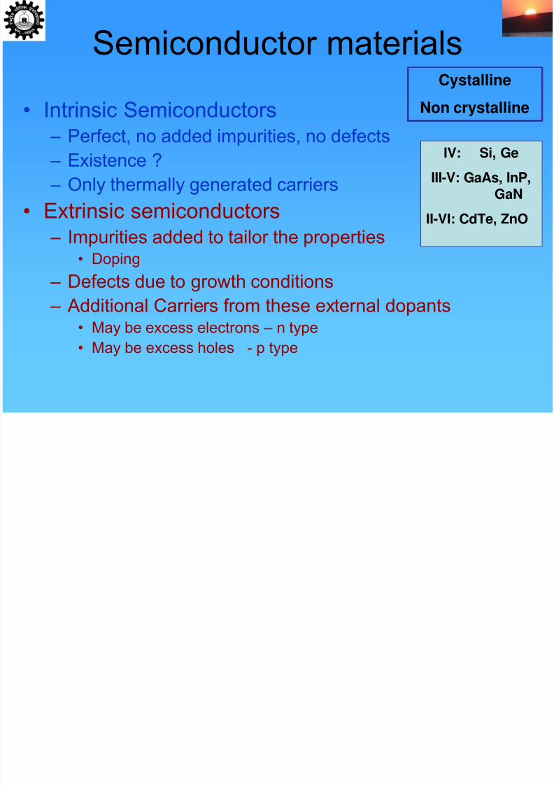
Semiconductor materials
• Intrinsic Semiconductors – Perfect, no added impurities, no defects
– Existence ?
– Only thermally generated carriers
• Extrinsic semiconductors – Impurities added to tailor the properties
• Doping
– Defects due to growth conditions
– Additional Carriers from these external dopants• May be excess electrons – n type
• May be excess holes - p type
Cystalline
Non crystalline
IV: Si, Ge
III-V: GaAs, InP,
GaNII-VI: CdTe, ZnO
7/29/2019 perspective in photovoltaics
http://slidepdf.com/reader/full/perspective-in-photovoltaics 43/148
45
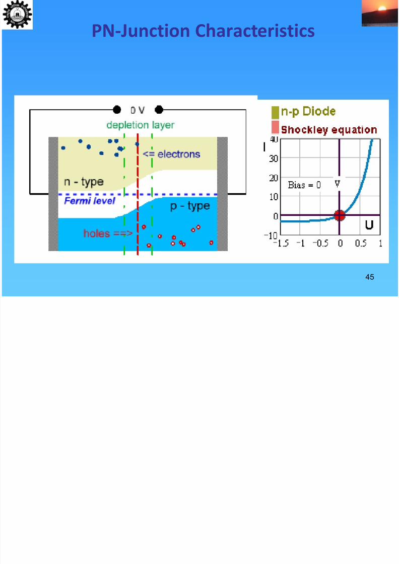
PN-Junction Characteristics
7/29/2019 perspective in photovoltaics
http://slidepdf.com/reader/full/perspective-in-photovoltaics 44/148
Semiconductors
Photo-Voltaic = PV
7/29/2019 perspective in photovoltaics
http://slidepdf.com/reader/full/perspective-in-photovoltaics 45/148
47
15x10
-3
10
5
0
-5
C u r r e n t d e n s i t y ( A / c m
2 )
1.20.80.40.0
Bias (V)
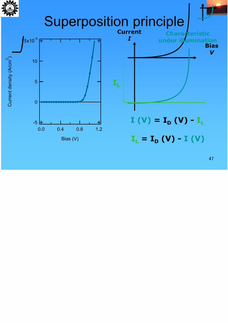
Superposition principle
I (V) = ID (V) - IL
Current I
BiasV
Characteristic
under illumination
IL = ID (V) - I (V)
IL
7/29/2019 perspective in photovoltaics
http://slidepdf.com/reader/full/perspective-in-photovoltaics 46/148
48
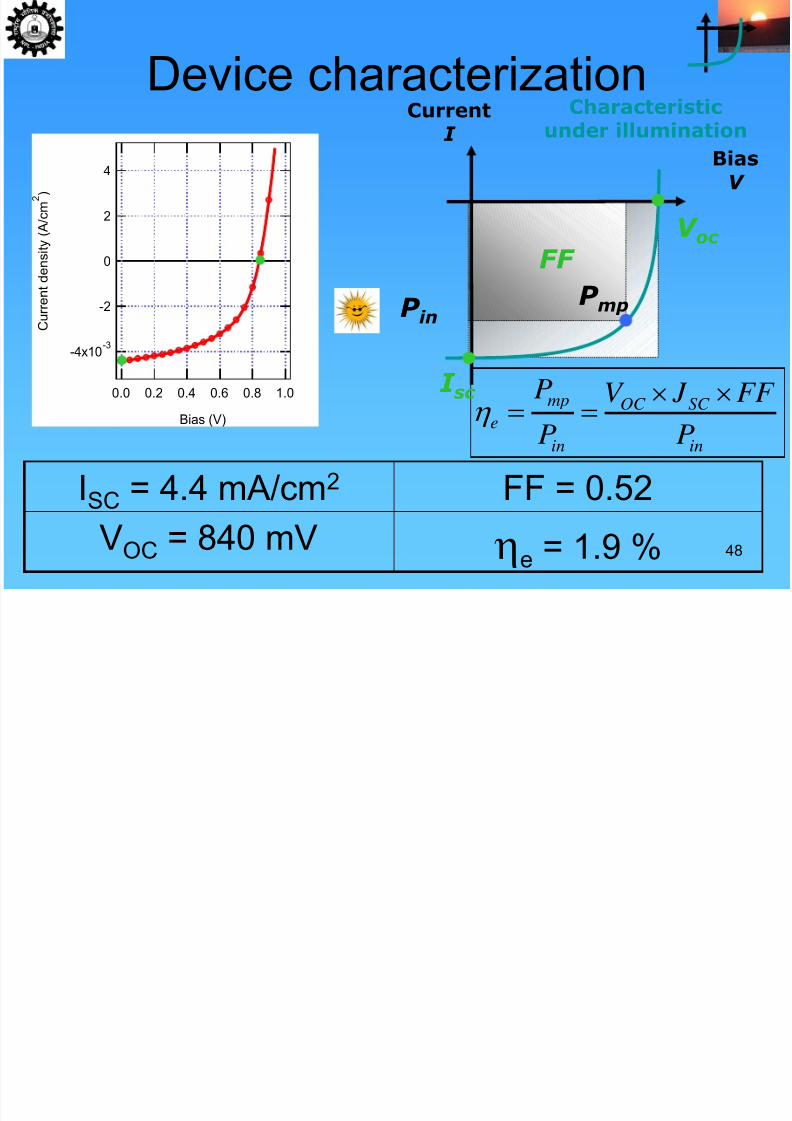
in
SC OC
in
mp
e P
FF J V
P
P
Device characterizationCurrent
I BiasV
I sc
V oc
Characteristicunder illumination
FF P mp P in
ISC = 4.4 mA/cm2 FF = 0.52
VOC
= 840 mVe = 1.9 %
-4x10⁻³
-2
0
2
4
C u r r e n t d e n s i t y ( A / c m
2 )
1.00.80.60.40.20.0
Bias (V)
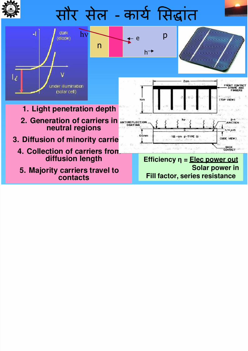
सौ सेऱ कायत साॊ
7/29/2019 perspective in photovoltaics
http://slidepdf.com/reader/full/perspective-in-photovoltaics 47/148
सौ सेऱ - कायत साॊ
101102
1. Light penetration depth
2. Generation of carriers inneutral regions
3. Diffusion of minority carriers
4. Collection of carriers fromdiffusion length
5. Majority carriers travel tocontacts
n
pe
h
h
Efficiency η = Elec power outSolar power in
Fill factor, series resistance
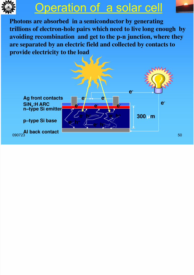
Operation of a solar cell
7/29/2019 perspective in photovoltaics
http://slidepdf.com/reader/full/perspective-in-photovoltaics 48/148
090723 50
Operation of a solar cell
b
Sb p –type Si base300 m
SiNx:H ARCn –type Si emitter
Al back contact
Ag front contacts
h+ h+ e- e-
e- e- h+
h+
e-
e-
e-
e-
Photons are absorbed in a semiconductor by generating
trillions of electron-hole pairs which need to live long enough by
avoiding recombination and get to the p-n junction, where theyare separated by an electric field and collected by contacts to
provide electricity to the load
e- e- e-
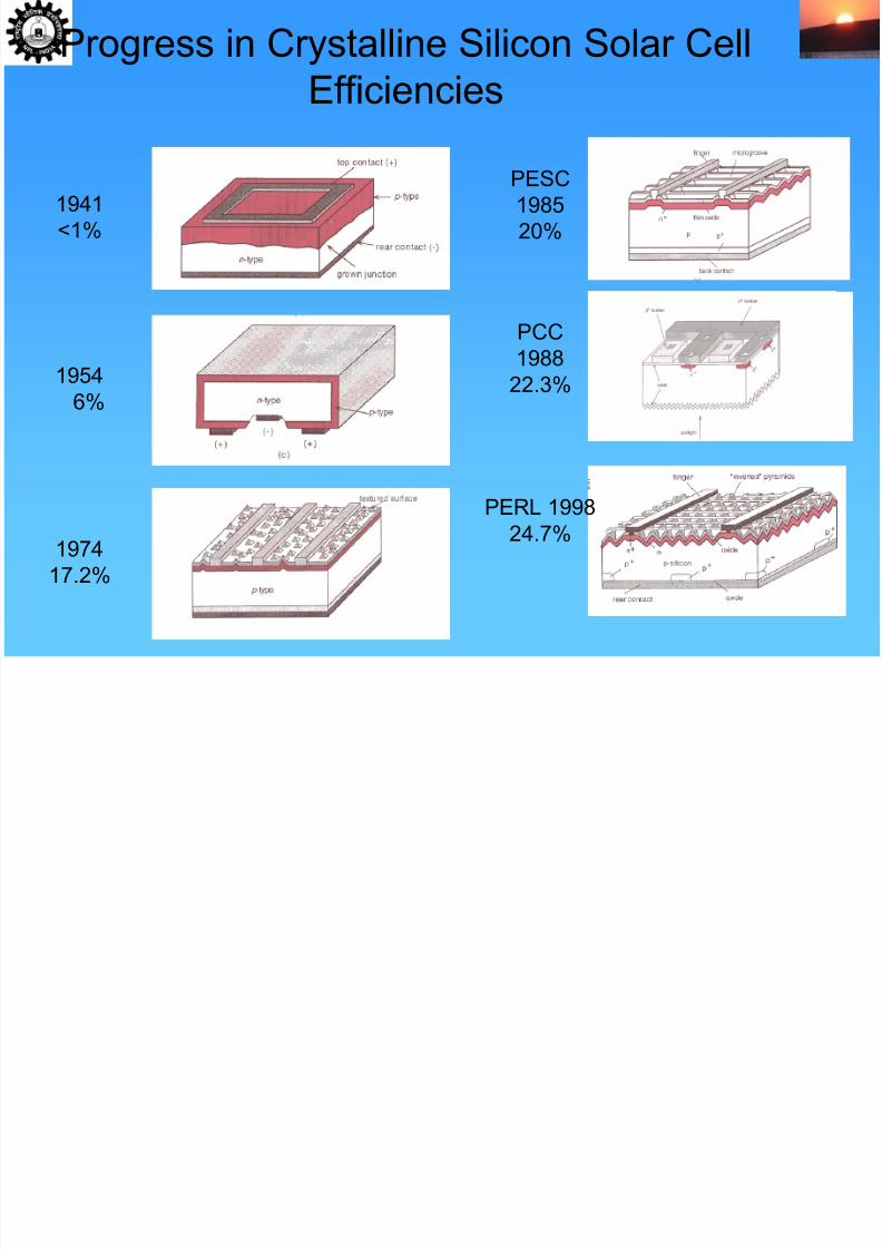
Progress in Crystalline Silicon Solar Cell
7/29/2019 perspective in photovoltaics
http://slidepdf.com/reader/full/perspective-in-photovoltaics 49/148
1941<1%
19546%
PESC198520%
PERL 199824.7%
197417.2%
PCC1988
22.3%
Progress in Crystalline Silicon Solar CellEfficiencies
7/29/2019 perspective in photovoltaics
http://slidepdf.com/reader/full/perspective-in-photovoltaics 50/148
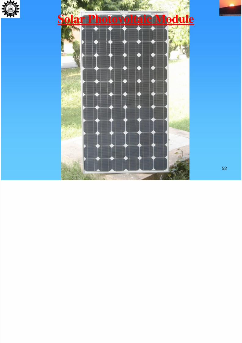
52
Solar Photovoltaic Module
7/29/2019 perspective in photovoltaics
http://slidepdf.com/reader/full/perspective-in-photovoltaics 51/148
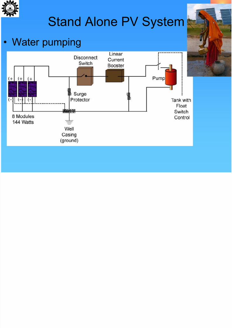
Stand Alone PV System
• Water pumping
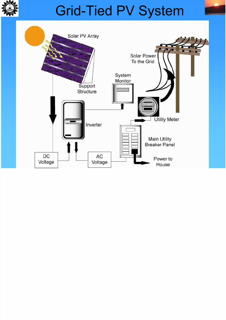
Grid Tied PV System
7/29/2019 perspective in photovoltaics
http://slidepdf.com/reader/full/perspective-in-photovoltaics 52/148
Grid-Tied PV System
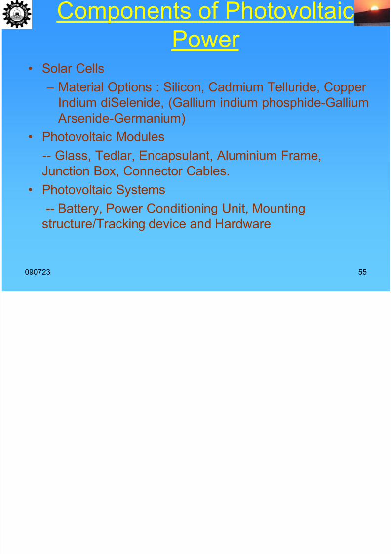
Components of Photovoltaic
7/29/2019 perspective in photovoltaics
http://slidepdf.com/reader/full/perspective-in-photovoltaics 53/148
090723 55
Components of PhotovoltaicPower
• Solar Cells – Material Options : Silicon, Cadmium Telluride, Copper
Indium diSelenide, (Gallium indium phosphide-Gallium Arsenide-Germanium)
• Photovoltaic Modules-- Glass, Tedlar, Encapsulant, Aluminium Frame,Junction Box, Connector Cables.
• Photovoltaic Systems
-- Battery, Power Conditioning Unit, Mountingstructure/Tracking device and Hardware
7/29/2019 perspective in photovoltaics
http://slidepdf.com/reader/full/perspective-in-photovoltaics 54/148
090723 56
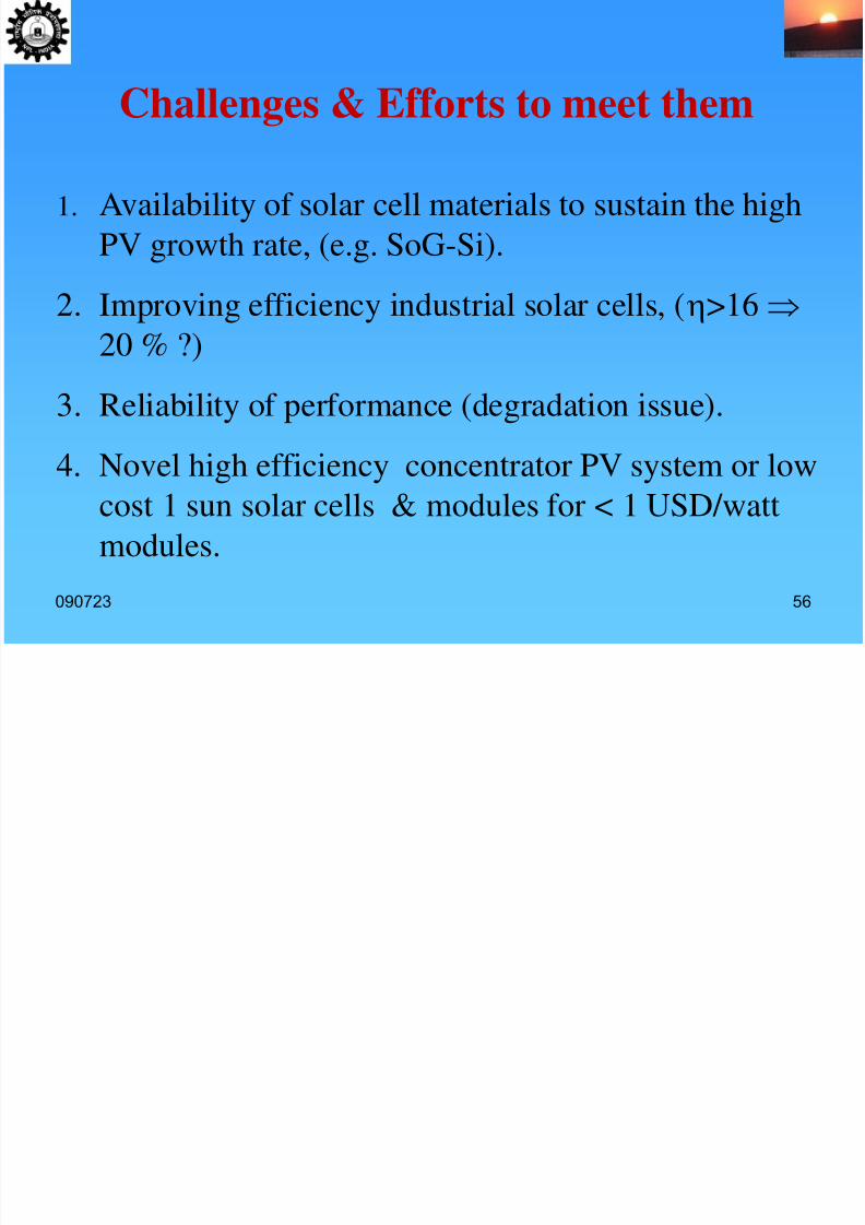
Challenges & Efforts to meet them
1. Availability of solar cell materials to sustain the high
PV growth rate, (e.g. SoG-Si).
2. Improving efficiency industrial solar cells, (>16 20 % ?)
3. Reliability of performance (degradation issue).
4. Novel high efficiency concentrator PV system or lowcost 1 sun solar cells & modules for < 1 USD/watt
modules.
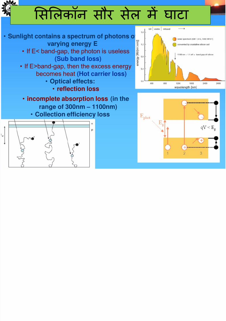
सऱकॉन सौ सेऱ म घाटा
7/29/2019 perspective in photovoltaics
http://slidepdf.com/reader/full/perspective-in-photovoltaics 55/148
• Sunlight contains a spectrum of photons of
varying energy E• If E< band-gap, the photon is useless
(Sub band loss)• If E>band-gap, then the excess energy
becomes heat (Hot carrier loss)
• Optical effects:• reflection loss
• incomplete absorption loss (in the
range of 300nm – 1100nm)• Collection efficiency loss
सऱकॉन सौ सेऱ म घाटा
7/29/2019 perspective in photovoltaics
http://slidepdf.com/reader/full/perspective-in-photovoltaics 56/148
–
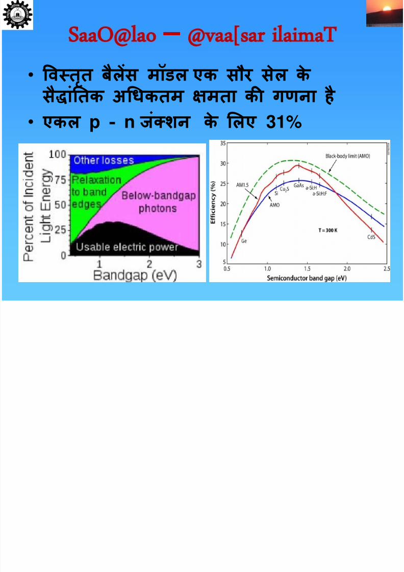
• वत तृ फैऱस मॉडऱ एक सौ सेऱ केसैजतक अधकतम ऺमतज क गणनज है
• एकऱ p - n रशन के ऱए 31%
7/29/2019 perspective in photovoltaics
http://slidepdf.com/reader/full/perspective-in-photovoltaics 57/148
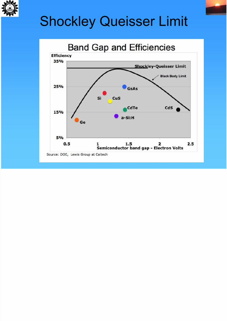
Shockley Queisser Limit
पोटोवोलटक
7/29/2019 perspective in photovoltaics
http://slidepdf.com/reader/full/perspective-in-photovoltaics 58/148
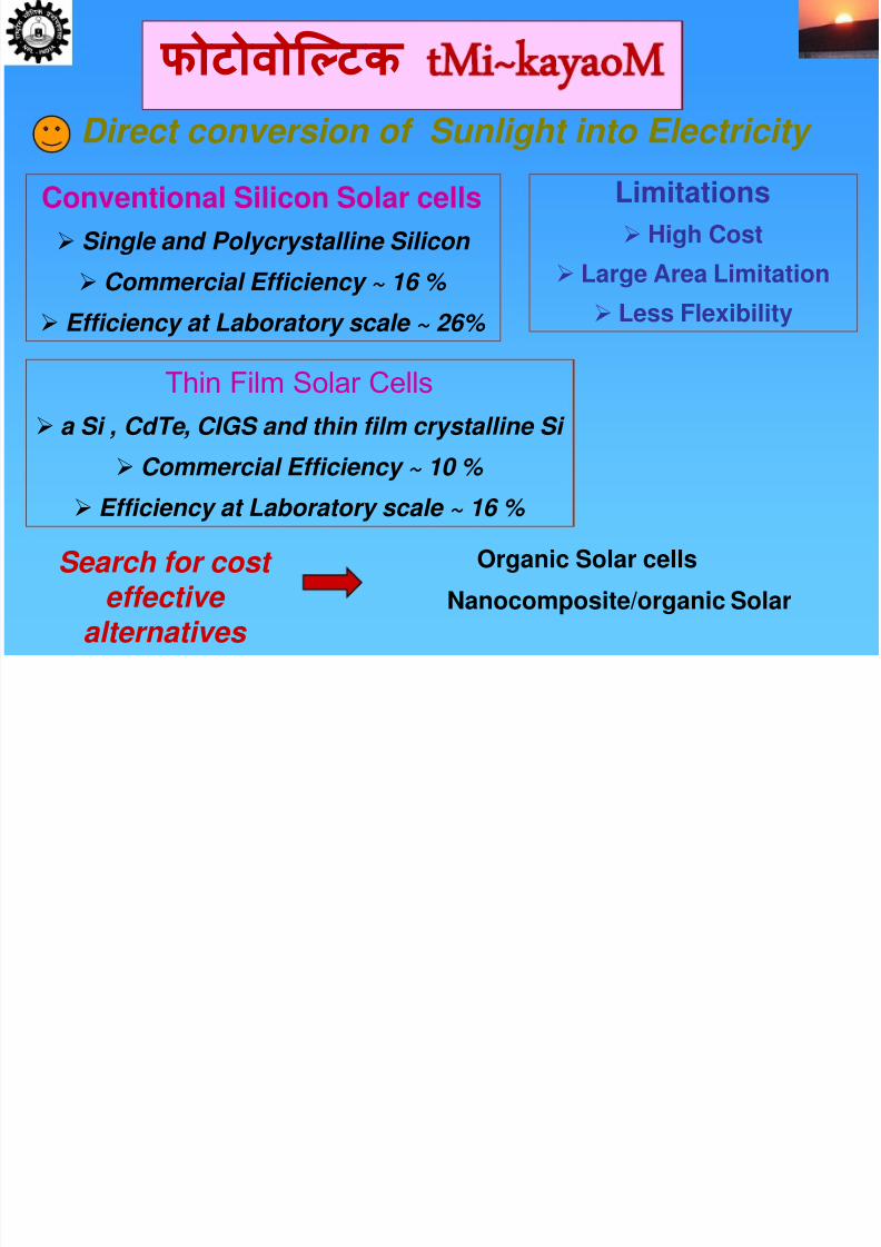
पोटोवोलटक Direct conversion of Sunlight into Electricity
Conventional Silicon Solar cells
Single and Polycrystalline Silicon
Commercial Efficiency ~ 16 %
Efficiency at Laboratory scale ~ 26%
Thin Film Solar Cells
a Si , CdTe, CIGS and thin film crystalline Si
Commercial Efficiency ~ 10 % Efficiency at Laboratory scale ~ 16 %
Limitations
High Cost
Large Area Limitation
Less Flexibility
Search for cost effective
alternatives
Nanocomposite/organic Solar
Organic Solar cells
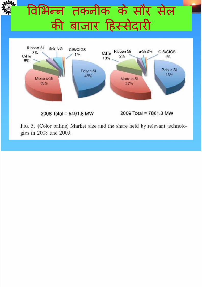
वभन कनीक के सौ सेऱ
7/29/2019 perspective in photovoltaics
http://slidepdf.com/reader/full/perspective-in-photovoltaics 59/148
वभन कनीक क सौ सऱ क बारा हसेदा
ी ौ े
7/29/2019 perspective in photovoltaics
http://slidepdf.com/reader/full/perspective-in-photovoltaics 60/148
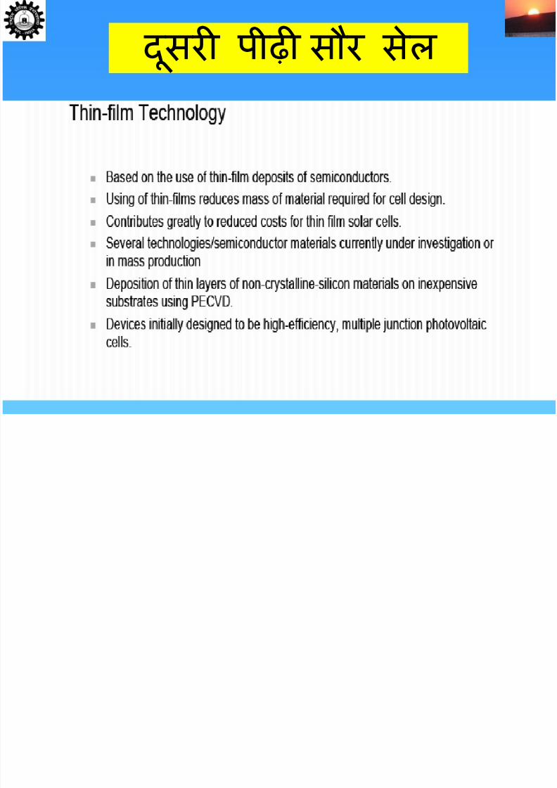
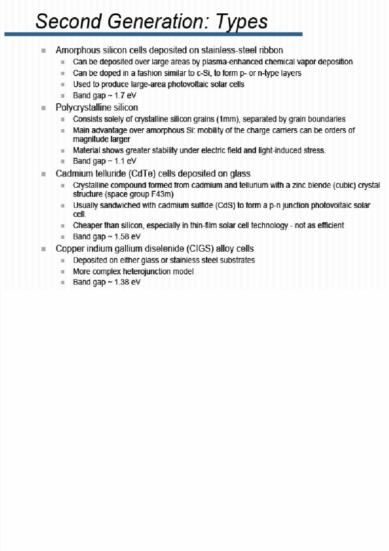
द सू पीढ सौ सेऱ
C ti l di f th t t f
7/29/2019 perspective in photovoltaics
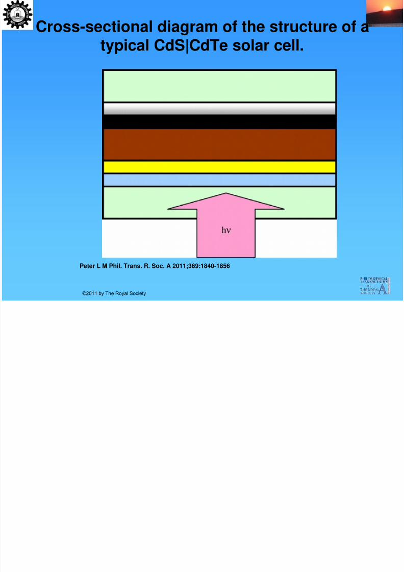
http://slidepdf.com/reader/full/perspective-in-photovoltaics 61/148
Cross-sectional diagram of the structure of atypical CdS|CdTe solar cell.
Peter L M Phil. Trans. R. Soc. A 2011;369:1840-1856
©2011 by The Royal Society
C ti l di f th t t f
7/29/2019 perspective in photovoltaics
http://slidepdf.com/reader/full/perspective-in-photovoltaics 62/148
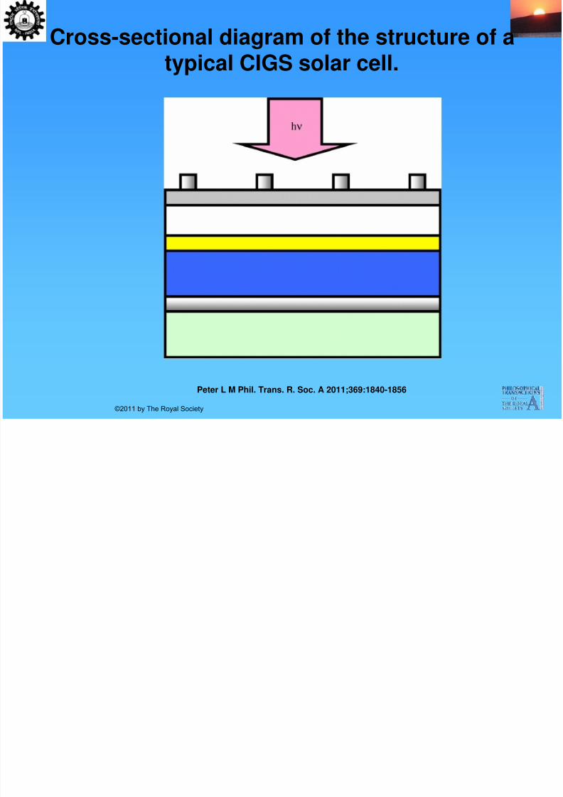
Cross-sectional diagram of the structure of atypical CIGS solar cell.
Peter L M Phil. Trans. R. Soc. A 2011;369:1840-1856
©2011 by The Royal Society
7/29/2019 perspective in photovoltaics
http://slidepdf.com/reader/full/perspective-in-photovoltaics 63/148
7/29/2019 perspective in photovoltaics
http://slidepdf.com/reader/full/perspective-in-photovoltaics 64/148
Harry Atwater, Albert Polman
nature materials, 9, 205, 2010
ी ी ौ े
7/29/2019 perspective in photovoltaics
http://slidepdf.com/reader/full/perspective-in-photovoltaics 65/148
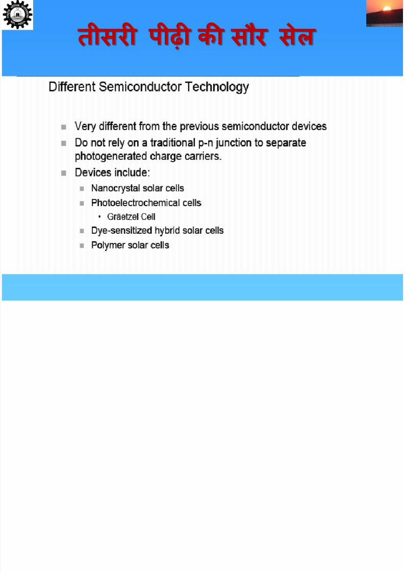
तीस ऩीढ क सौ सेऱ
7/29/2019 perspective in photovoltaics
http://slidepdf.com/reader/full/perspective-in-photovoltaics 66/148
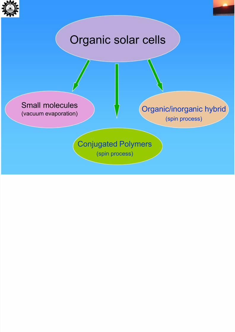
Organic solar cells
Small molecules(vacuum evaporation)
Conjugated Polymers(spin process)
Organic/inorganic hybrid(spin process)
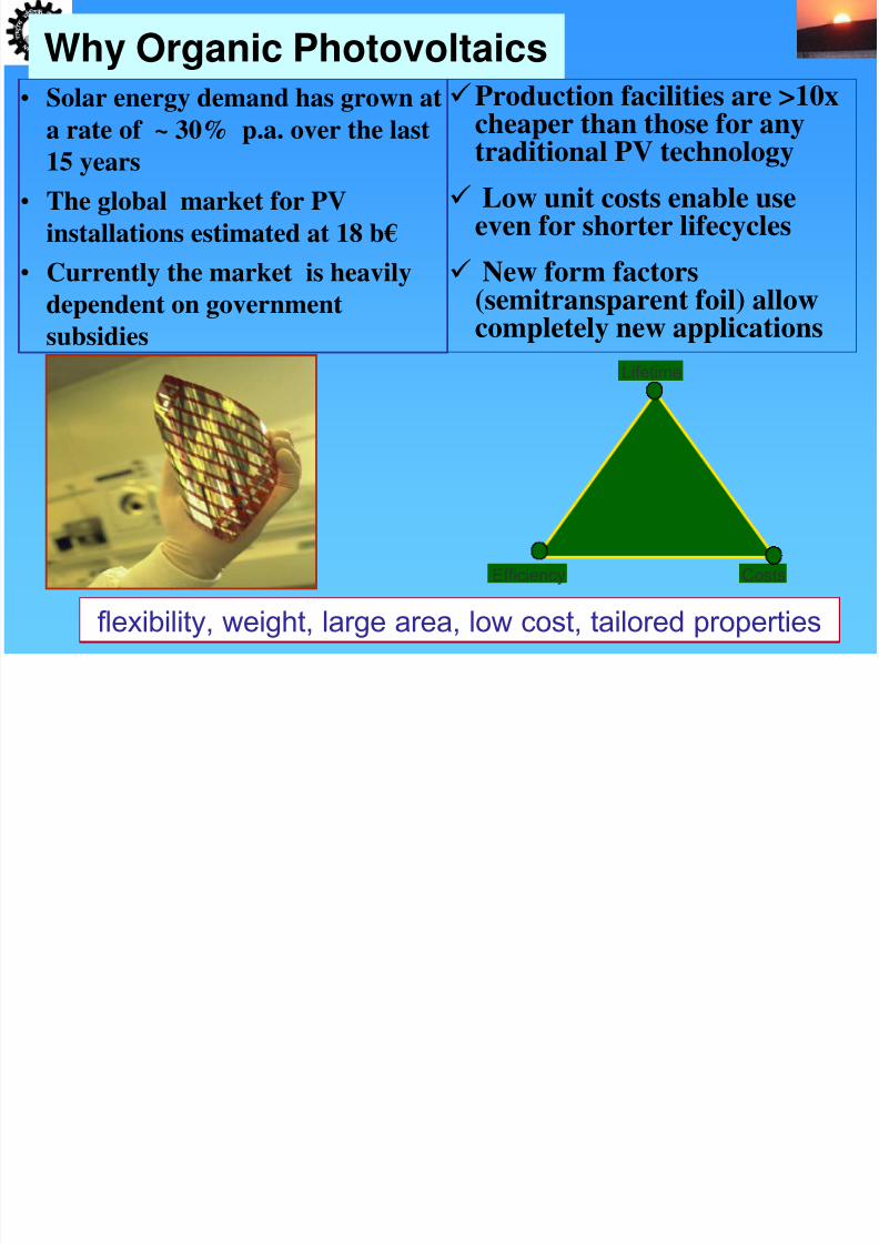
Why Organic Photovoltaics
7/29/2019 perspective in photovoltaics
http://slidepdf.com/reader/full/perspective-in-photovoltaics 67/148
69
Why Organic Photovoltaics• Solar energy demand has grown at
a rate of ~ 30% p.a. over the last
15 years• The global market for PV
installations estimated at 18 b €
• Currently the market is heavily
dependent on government
subsidies
Production facilities are >10xcheaper than those for any
traditional PV technology Low unit costs enable use
even for shorter lifecycles
New form factors(semitransparent foil) allowcompletely new applications
flexibility, weight, large area, low cost, tailored properties
Costs
Lifetime
Efficiency
7/29/2019 perspective in photovoltaics
http://slidepdf.com/reader/full/perspective-in-photovoltaics 68/148
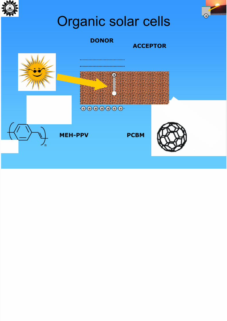
Organic solar cells
DONOR ACCEPTOR
O
MeOn
MEH-PPV PCBM
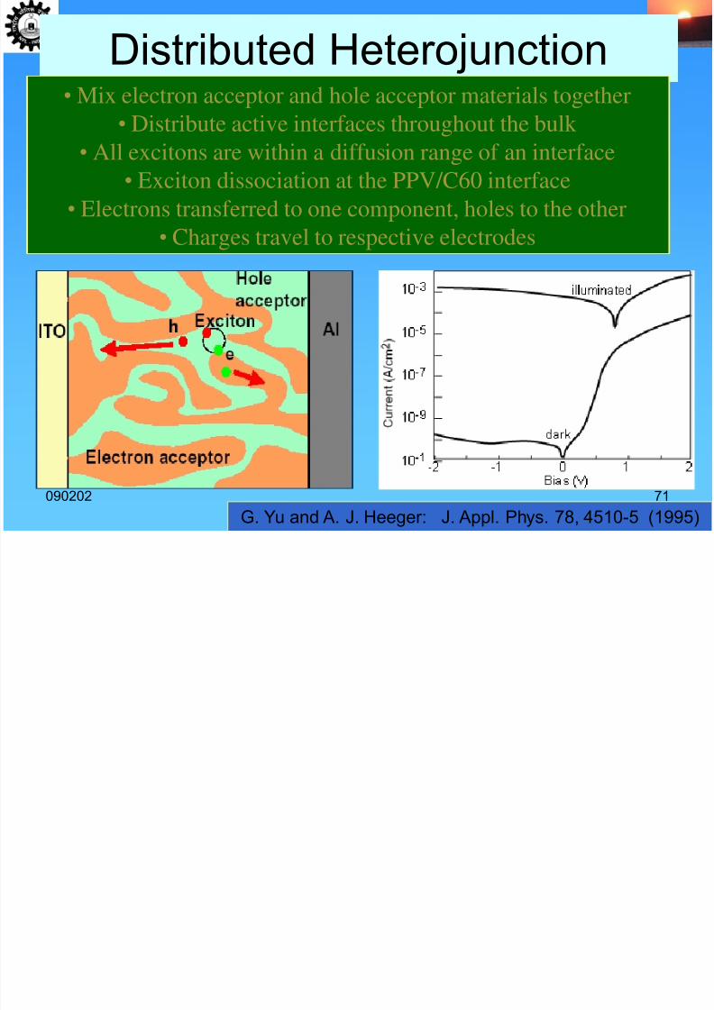
Distributed Heterojunction
7/29/2019 perspective in photovoltaics
http://slidepdf.com/reader/full/perspective-in-photovoltaics 69/148
090202 71
Distributed Heterojunction
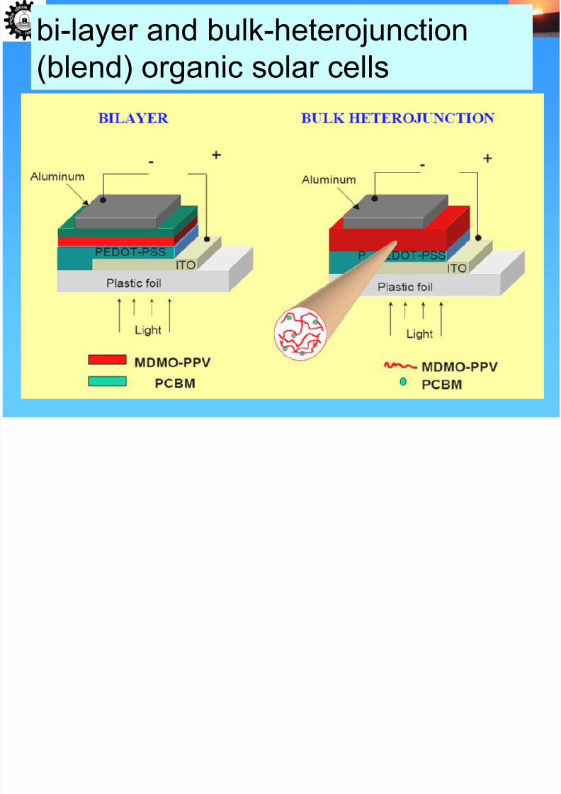
G. Yu and A. J. Heeger: J. Appl. Phys. 78, 4510-5 (1995)
• Mix electron acceptor and hole acceptor materials together
• Distribute active interfaces throughout the bulk • All excitons are within a diffusion range of an interface
• Exciton dissociation at the PPV/C60 interface
• Electrons transferred to one component, holes to the other
• Charges travel to respective electrodes
bi-layer and bulk-heterojunction
7/29/2019 perspective in photovoltaics
http://slidepdf.com/reader/full/perspective-in-photovoltaics 70/148
090202 72
bi layer and bulk heterojunction(blend) organic solar cells
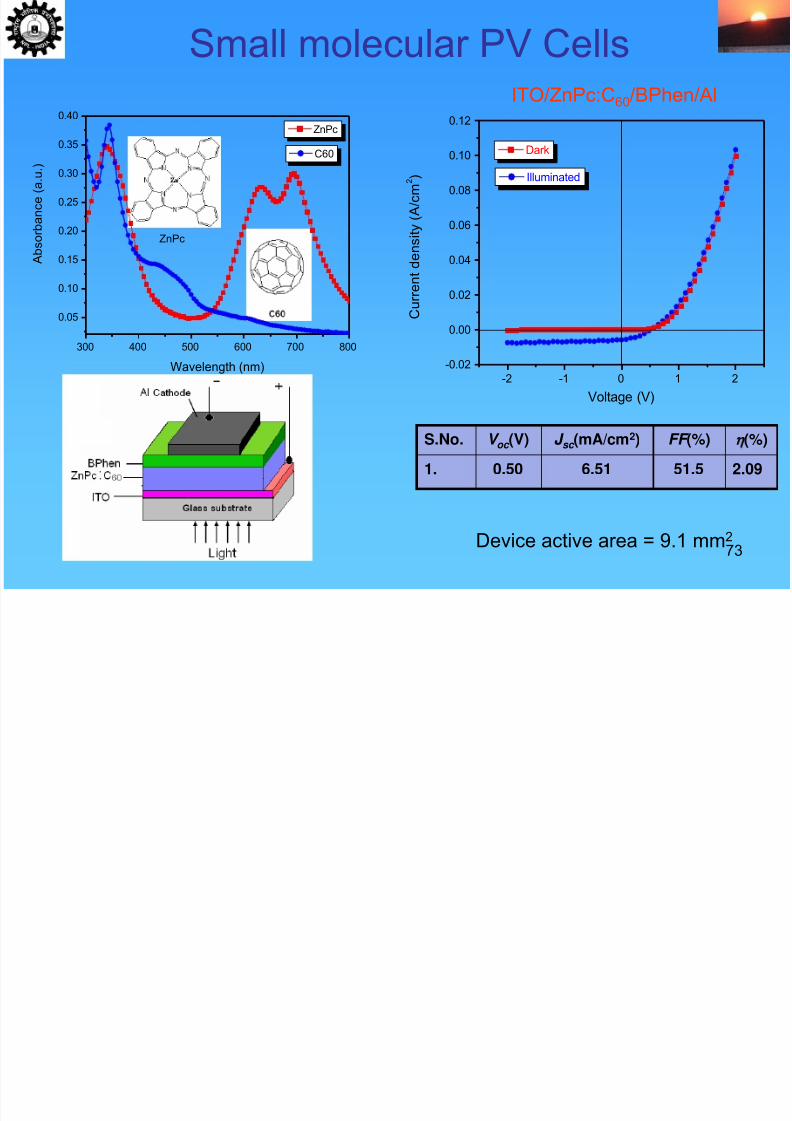
Small molecular PV Cells
7/29/2019 perspective in photovoltaics
http://slidepdf.com/reader/full/perspective-in-photovoltaics 71/148
73
Small molecular PV Cells
S.No. V oc (V) J sc (mA/cm2) FF (%) (%)
1. 0.50 6.51 51.5 2.09
-2 -1 0 1 2
-0.02
0.00
0.02
0.04
0.06
0.08
0.10
0.12
C u r r e
n t d e n s i t y ( A / c m
2 )
Voltage (V)
Illuminated
Dark
ZnPc
Device active area = 9.1 mm2
ITO/ZnPc:C60/BPhen/Al
0.05
0.10
0.15
0.20
0.25
0.30
0.35
0.40
300 400 500 600 700 800
A b s o r b a n c e ( a . u . )
Wavelength (nm)
ZnPc
C60
7/29/2019 perspective in photovoltaics
http://slidepdf.com/reader/full/perspective-in-photovoltaics 72/148
7/29/2019 perspective in photovoltaics
http://slidepdf.com/reader/full/perspective-in-photovoltaics 73/148
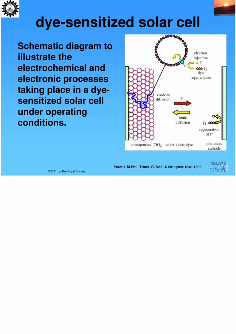
Schematic diagram toillustrate theelectrochemical andelectronic processestaking place in a dye-sensitized solar cellunder operating
conditions.
Peter L M Phil. Trans. R. Soc. A 2011;369:1840-1856©2011 by The Royal Society
dye-sensitized solar cell
7/29/2019 perspective in photovoltaics
http://slidepdf.com/reader/full/perspective-in-photovoltaics 74/148
ौ े ी ौ े
7/29/2019 perspective in photovoltaics
http://slidepdf.com/reader/full/perspective-in-photovoltaics 75/148
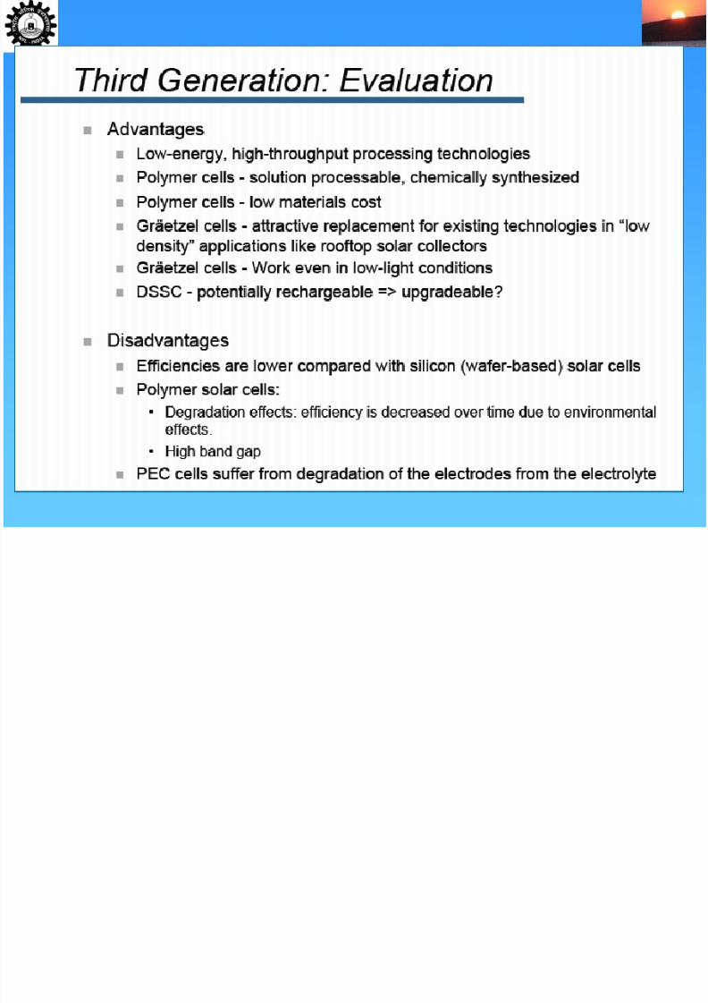
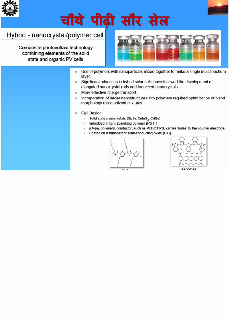
चौथे ऩीढ सौ सेऱ
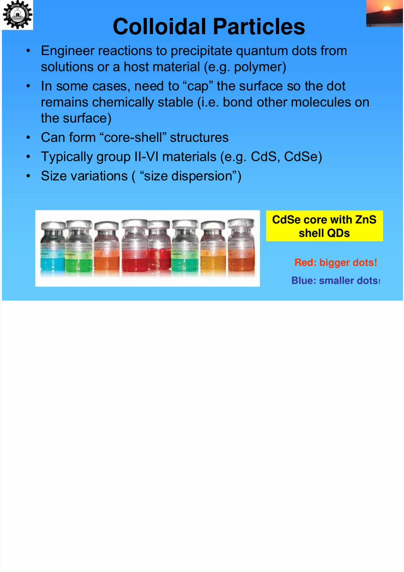
Colloidal Particles
7/29/2019 perspective in photovoltaics
http://slidepdf.com/reader/full/perspective-in-photovoltaics 76/148
Colloidal Particles• Engineer reactions to precipitate quantum dots from
solutions or a host material (e.g. polymer)
• In some cases, need to “cap” the surface so the dot
remains chemically stable (i.e. bond other molecules onthe surface)
• Can form “core-shell” structures
• Typically group II-VI materials (e.g. CdS, CdSe)
• Size variations ( “size dispersion”)
CdSe core with ZnSshell QDs
Red: bigger dots!
Blue: smaller dots!
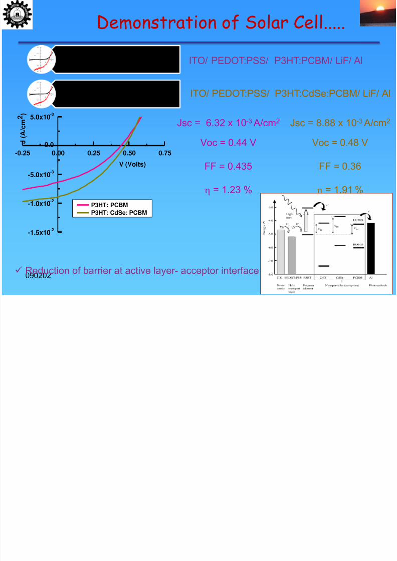
Demonstration of Solar Cell.....
7/29/2019 perspective in photovoltaics
http://slidepdf.com/reader/full/perspective-in-photovoltaics 77/148
090202 79
Demonstration of Solar Cell.....
P3HT: PCBM
P3HT: CdSe: PCBM
Jsc = 6.32 x 10⁻³ A/cm2
Voc = 0.44 V
FF = 0.435
= 1.23 %
Jsc = 8.88 x 10⁻³ A/cm2
Voc = 0.48 V
FF = 0.36
= 1.91 %
ITO/ PEDOT:PSS/ P3HT:PCBM/ LiF/ Al
ITO/ PEDOT:PSS/ P3HT:CdSe:PCBM/ LiF/ Al
Reduction of barrier at active layer- acceptor interface
-0.25 0.00 0.25 0.50 0.75
-1.5x10⁻²
-1.0x10⁻²
-5.0x10⁻³
0.0
5.0x10⁻³
P3HT: PCBM
P3HT: CdSe: PCBM
J ( A / c m
2 )
V (Volts)
Demonstration of Solar Cell.....
7/29/2019 perspective in photovoltaics
http://slidepdf.com/reader/full/perspective-in-photovoltaics 78/148
090202 80
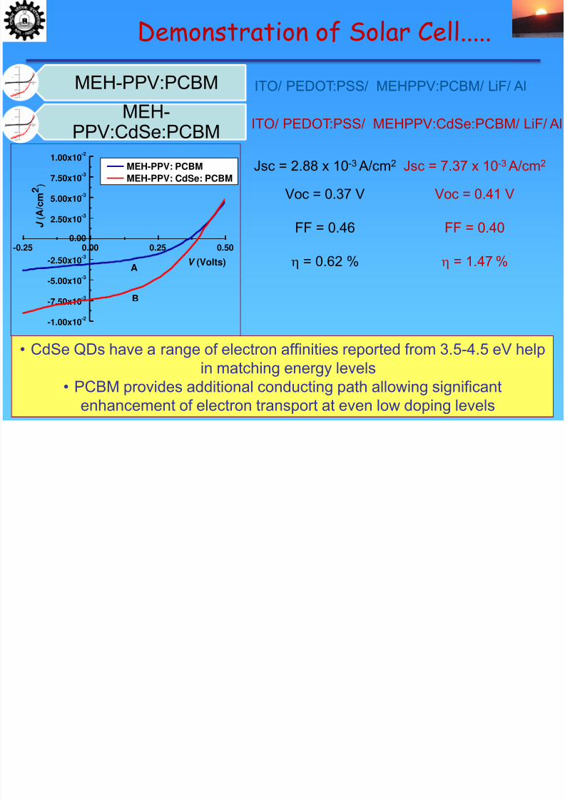
Demonstration of Solar Cell.....
MEH-PPV:PCBM
MEH-PPV:CdSe:PCBM
Jsc = 2.88 x 10⁻³ A/cm2
Voc = 0.37 V
FF = 0.46
= 0.62 %
Jsc = 7.37 x 10⁻³ A/cm2
Voc = 0.41 V
FF = 0.40
= 1.47 %
ITO/ PEDOT:PSS/ MEHPPV:PCBM/ LiF/ Al
ITO/ PEDOT:PSS/ MEHPPV:CdSe:PCBM/ LiF/ Al
-0.25 0.00 0.25 0.50
-1.00x10⁻²
-7.50x10
-3
-5.00x10⁻³
-2.50x10⁻³
0.00
2.50x10⁻³
5.00x10⁻³
7.50x10⁻³
1.00x10⁻²
B
MEH-PPV: PCBM
MEH-PPV: CdSe: PCBM
J
( A / c
m 2 )
V (Volts)A
• CdSe QDs have a range of electron affinities reported from 3.5-4.5 eV helpin matching energy levels
• PCBM provides additional conducting path allowing significant
enhancement of electron transport at even low doping levels
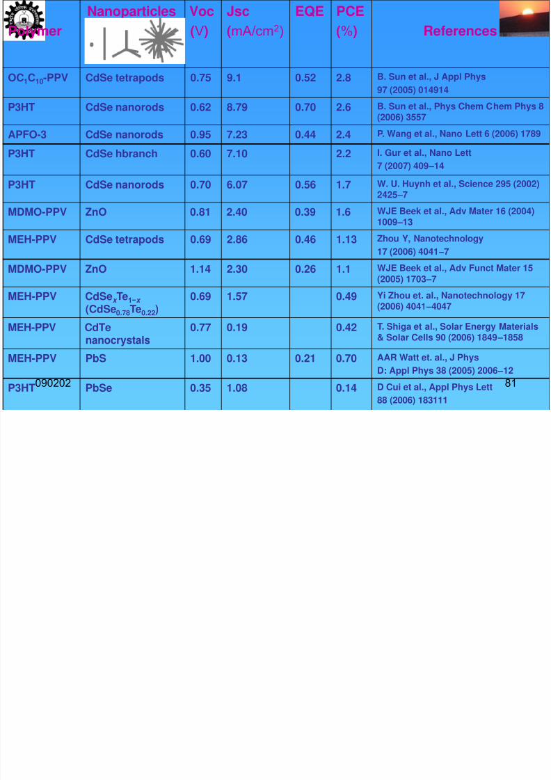
PolymerNanoparticles Voc
(V)Jsc(mA/cm2)
EQE PCE(%) References
7/29/2019 perspective in photovoltaics
http://slidepdf.com/reader/full/perspective-in-photovoltaics 79/148
090202 81
OC1C10-PPV CdSe tetrapods 0.75 9.1 0.52 2.8 B. Sun et al., J Appl Phys
97 (2005) 014914
P3HT CdSe nanorods 0.62 8.79 0.70 2.6 B. Sun et al., Phys Chem Chem Phys 8(2006) 3557
APFO-3 CdSe nanorods 0.95 7.23 0.44 2.4 P. Wang et al., Nano Lett 6 (2006) 1789
P3HT CdSe hbranch 0.60 7.10 2.2 I. Gur et al., Nano Lett
7 (2007) 409 –14
P3HT CdSe nanorods 0.70 6.07 0.56 1.7 W. U. Huynh et al., Science 295 (2002)2425 –7
MDMO-PPV ZnO 0.81 2.40 0.39 1.6 WJE Beek et al., Adv Mater 16 (2004)1009 –13
MEH-PPV CdSe tetrapods 0.69 2.86 0.46 1.13 Zhou Y, Nanotechnology
17 (2006) 4041 –7
MDMO-PPV ZnO 1.14 2.30 0.26 1.1 WJE Beek et al., Adv Funct Mater 15(2005) 1703 –7
MEH-PPV CdSex Te1−x (CdSe0.78Te0.22)
0.69 1.57 0.49 Yi Zhou et. al., Nanotechnology 17(2006) 4041 –4047
MEH-PPV CdTenanocrystals
0.77 0.19 0.42 T. Shiga et al., Solar Energy Materials& Solar Cells 90 (2006) 1849 –1858
MEH-PPV PbS 1.00 0.13 0.21 0.70 AAR Watt et. al., J Phys
D: Appl Phys 38 (2005) 2006 –12
P3HT PbSe 0.35 1.08 0.14D Cui et al., Appl Phys Lett
88 (2006) 183111
Hybrid Organic-Inorganic Solar Cells
7/29/2019 perspective in photovoltaics
http://slidepdf.com/reader/full/perspective-in-photovoltaics 80/148
y g g
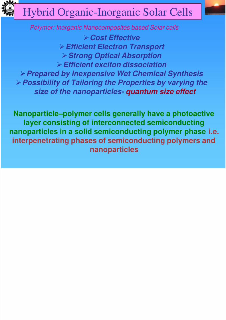
Polymer: Inorganic Nanocomposites based Solar cells
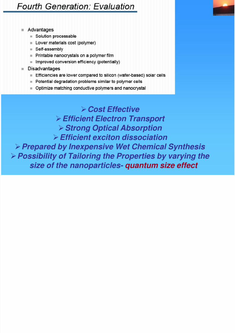
Cost Effective Efficient Electron Transport Strong Optical Absorption Efficient exciton dissociation
Prepared by Inexpensive Wet Chemical Synthesis
Possibility of Tailoring the Properties by varying the size of the nanoparticles- quantum size effect
Nanoparticle –polymer cells generally have a photoactive
layer consisting of interconnected semiconductingnanoparticles in a solid semiconducting polymer phase i.e.interpenetrating phases of semiconducting polymers and
nanoparticles
-
Luminescent Graphene Quantum Dots (GQDs) for Organic Photovoltaics Devices
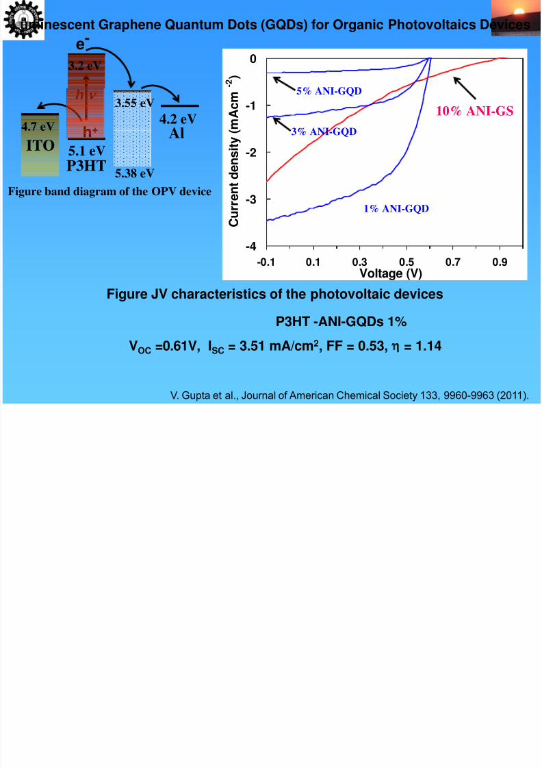
7/29/2019 perspective in photovoltaics
http://slidepdf.com/reader/full/perspective-in-photovoltaics 81/148
-4
-3
-2
-1
0
-0.1 0.1 0.3 0.5 0.7 0.9Voltage (V)
C u r r e
n t d e n s i t y ( m A c m
- 2 )
10% ANI-GS
5% ANI-GQD
3% ANI-GQD
1% ANI-GQD
P3HT
Al
5.1 eV
4.2 eVh+
e-
4.7 eV
ITO
h
3.2 eV
3.55 eV
5.38 eV
Figure band diagram of the OPV device
P3HT -ANI-GQDs 1%
VOC =0.61V, ISC = 3.51 mA/cm2, FF = 0.53, = 1.14
Figure JV characteristics of the photovoltaic devices
V. Gupta et al., Journal of American Chemical Society 133, 9960-9963 (2011).
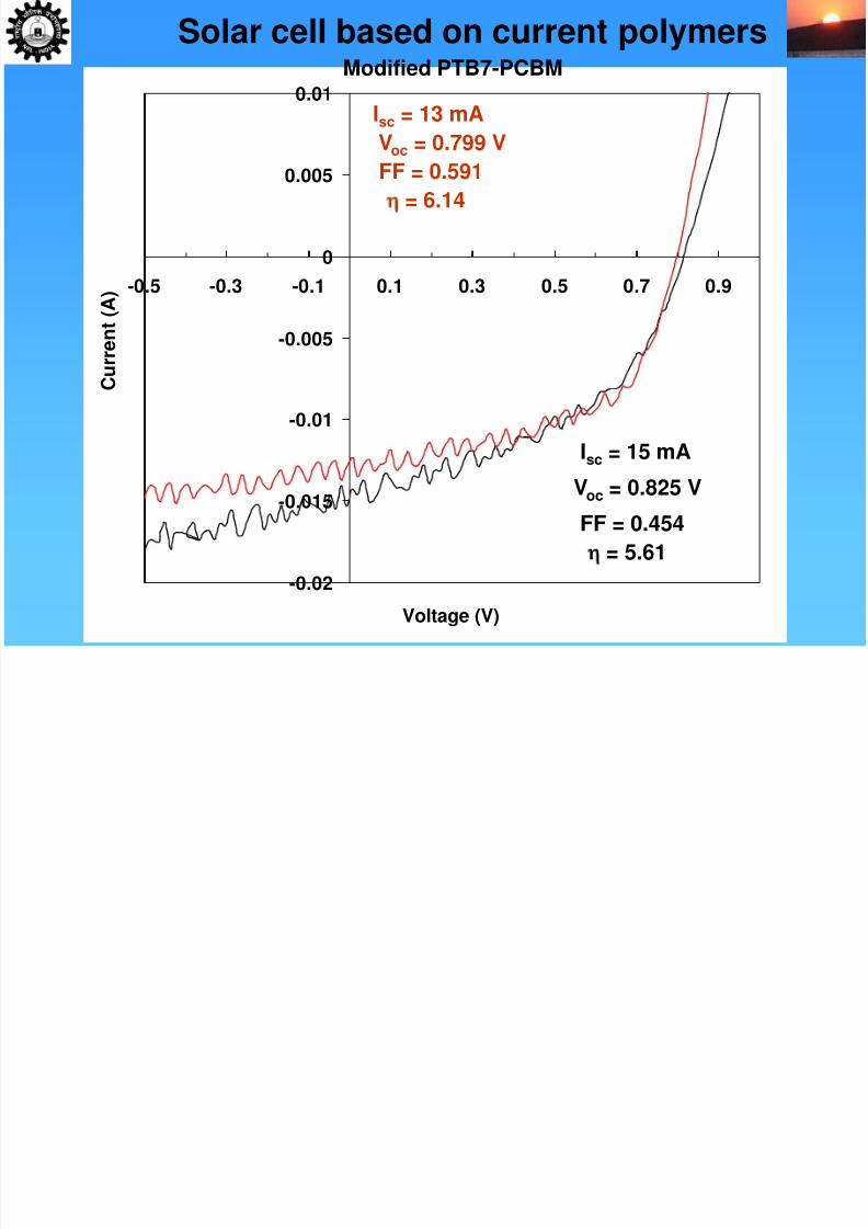
Modified PTB7 PCBM
Solar cell based on current polymers
7/29/2019 perspective in photovoltaics
http://slidepdf.com/reader/full/perspective-in-photovoltaics 82/148
-0.02
-0.015
-0.01
-0.005
0
0.005
0.01
-0.5 -0.3 -0.1 0.1 0.3 0.5 0.7 0.9
Voltage (V)
C u r r e n t ( A )
Isc = 13 mA
Voc = 0.799 V
FF = 0.591= 6.14
Isc = 15 mA
Voc = 0.825 V
FF = 0.454
= 5.61
Modified PTB7-PCBM
Poly[[4,8-bis[(2-ethylhexyl)oxy]benzo[1,2-b:4,5-
b']dithiophene 2 6 di l]
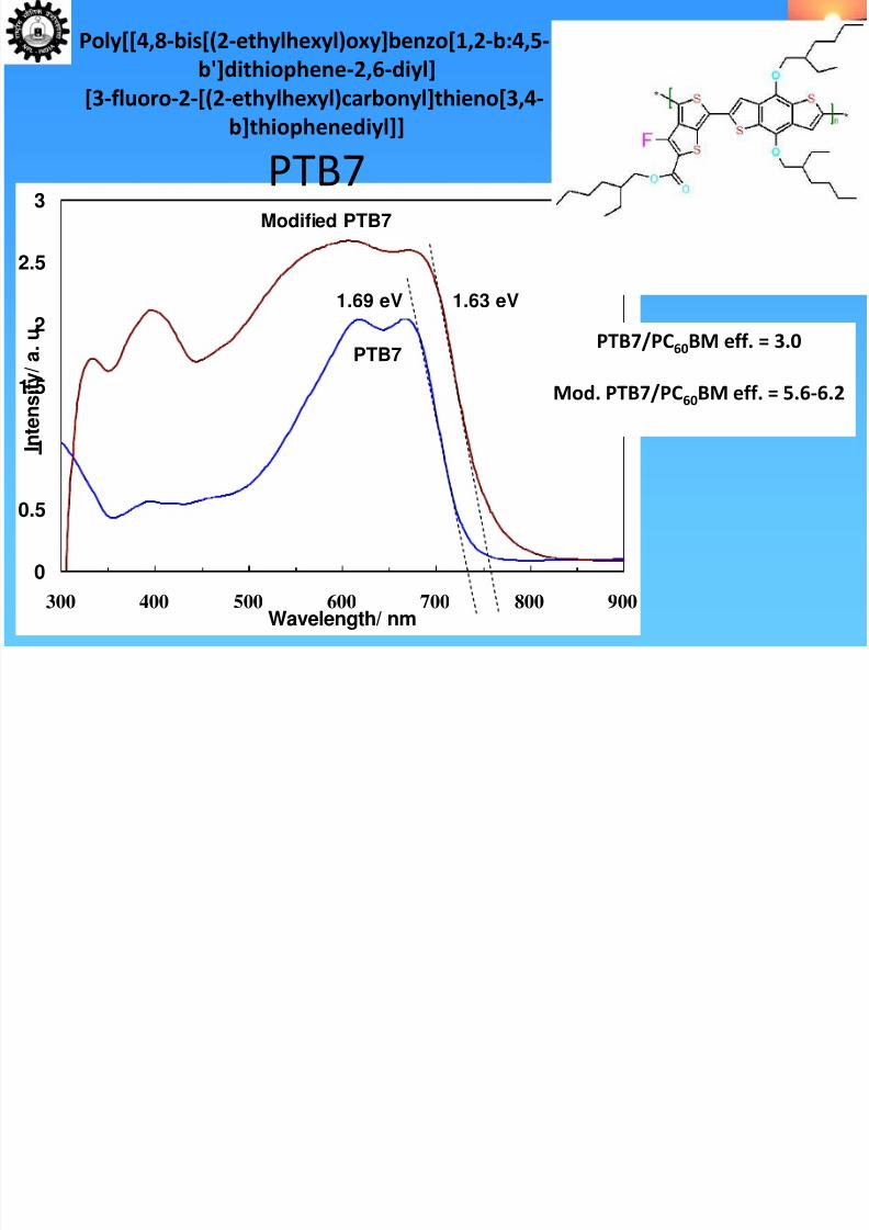
7/29/2019 perspective in photovoltaics
http://slidepdf.com/reader/full/perspective-in-photovoltaics 83/148
0
0.5
1
1.5
2
2.5
3
300 400 500 600 700 800 900
Wavelength/ nm
I n t e n s i t y / a . u .
1.69 eV 1.63 eV
PTB7
Modified PTB7
b']dithiophene-2,6-diyl]
[3-fluoro-2-[(2-ethylhexyl)carbonyl]thieno[3,4-
b]thiophenediyl]]
PTB7
PTB7/PC60BM eff. = 3.0
Mod. PTB7/PC60BM eff. = 5.6-6.2
7/29/2019 perspective in photovoltaics
http://slidepdf.com/reader/full/perspective-in-photovoltaics 84/148
Cost Effective Efficient Electron Transport
Strong Optical Absorption Efficient exciton dissociation
Prepared by Inexpensive Wet Chemical Synthesis Possibility of Tailoring the Properties by varying the
size of the nanoparticles- quantum size effect
7/29/2019 perspective in photovoltaics
http://slidepdf.com/reader/full/perspective-in-photovoltaics 85/148
7/29/2019 perspective in photovoltaics
http://slidepdf.com/reader/full/perspective-in-photovoltaics 86/148
7/29/2019 perspective in photovoltaics
http://slidepdf.com/reader/full/perspective-in-photovoltaics 87/148
ऊरात ऱौटाने का समय Energy payback time
7/29/2019 perspective in photovoltaics
http://slidepdf.com/reader/full/perspective-in-photovoltaics 88/148
Breakdown of EPT for three PV technologies based on data given by Wild-Schoten [27].
Peter L M Phil. Trans. R. Soc. A 2011;369:1840-1856
©2011 by The Royal Society
gy p y
From top to bottom for c-Si:Si feedstock, Ingot + wafer,cell, laminate, mounting and
cabling, inverter, recycling.
From bottom to top for CIGSand CdTe: laminate,
mounting and cabling,inverter, recycling.
Current Manufacturers of
7/29/2019 perspective in photovoltaics
http://slidepdf.com/reader/full/perspective-in-photovoltaics 89/148
090723 9191
Silicon Feed Stock 2008(Actual)
(MT)Hemlock, USA 15500
Wacker, Germany 11100
Tokuyama, Japan 5900
REC, USA 6100Mitsubishi, Japan/USA 3400
MEMC, Italy/USA 5600
DC Chemicals 3100
Dow Corning 3000
M Setek 2500GCL 1800
Others 12000
TOTAL 70000
Technology Shares
7/29/2019 perspective in photovoltaics
http://slidepdf.com/reader/full/perspective-in-photovoltaics 90/148
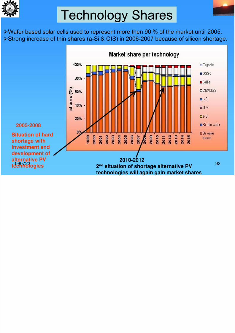
090723 92
Technology SharesWafer based solar cells used to represent more then 90 % of the market until 2005.Strong increase of thin shares (a-Si & CIS) in 2006-2007 because of silicon shortage.
2005-2008Situation of hardshortage withinvestment anddevelopment ofalternative PV
technologies
2010-2012
2nd
situation of shortage alternative PVtechnologies will again gain market shares
Current Manufacturing Costs
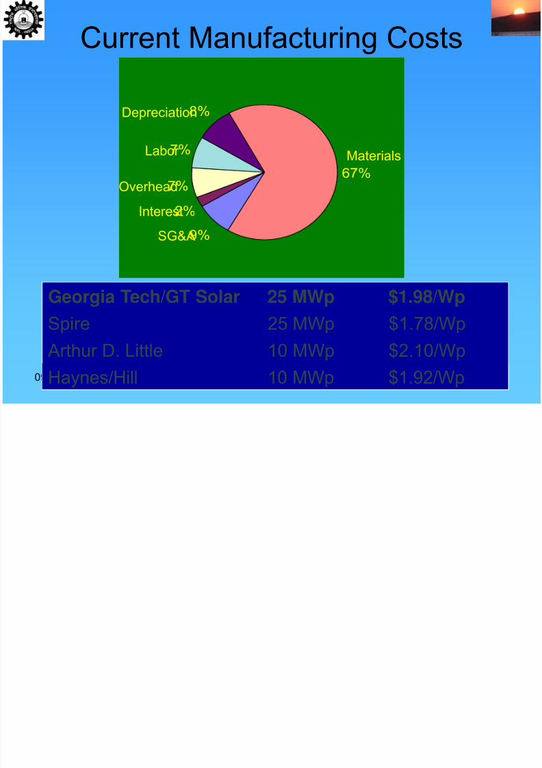
7/29/2019 perspective in photovoltaics
http://slidepdf.com/reader/full/perspective-in-photovoltaics 91/148
090723 93
Current Manufacturing Costs
9%
2%
7%
7%
8%
67%
Georgia Tech/GT Solar 25 MWp $1.98/WpSpire 25 MWp $1.78/Wp
Arthur D. Little 10 MWp $2.10/Wp
Haynes/Hill 10 MWp $1.92/Wp
Materials
Depreciation
Labor
Overhead
Interest
SG&A
Economic Roadmap for Low-
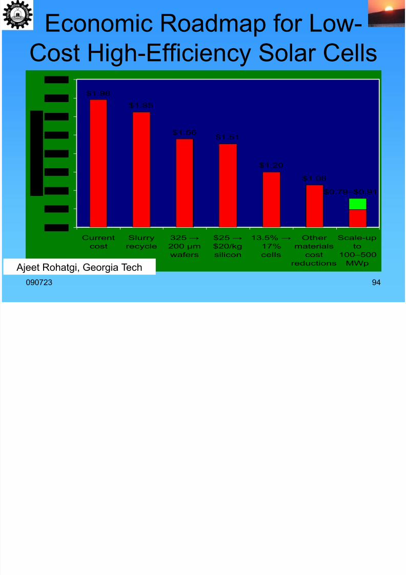
7/29/2019 perspective in photovoltaics
http://slidepdf.com/reader/full/perspective-in-photovoltaics 92/148
090723 94
pCost High-Efficiency Solar Cells
$0.79–$0.91
$1.06
$1.20
$1.51$1.56
$1.85
$1.98
$0.60
$0.80
$1.00
$1.20
$1.40
$1.60
$1.80
$2.00
$2.20
Current
cost
Slurry
recycle
325 →
200 µm
wafers
$25 →
$20/kg
silicon
13.5% →
17%
cells
Other
materials
cost
reductions
Scale-up
to
100–500
MWp
M a n u f a c t u r i n g C o s t ( p e r W p )
Ajeet Rohatgi, Georgia Tech
Projected module manufacturing cost
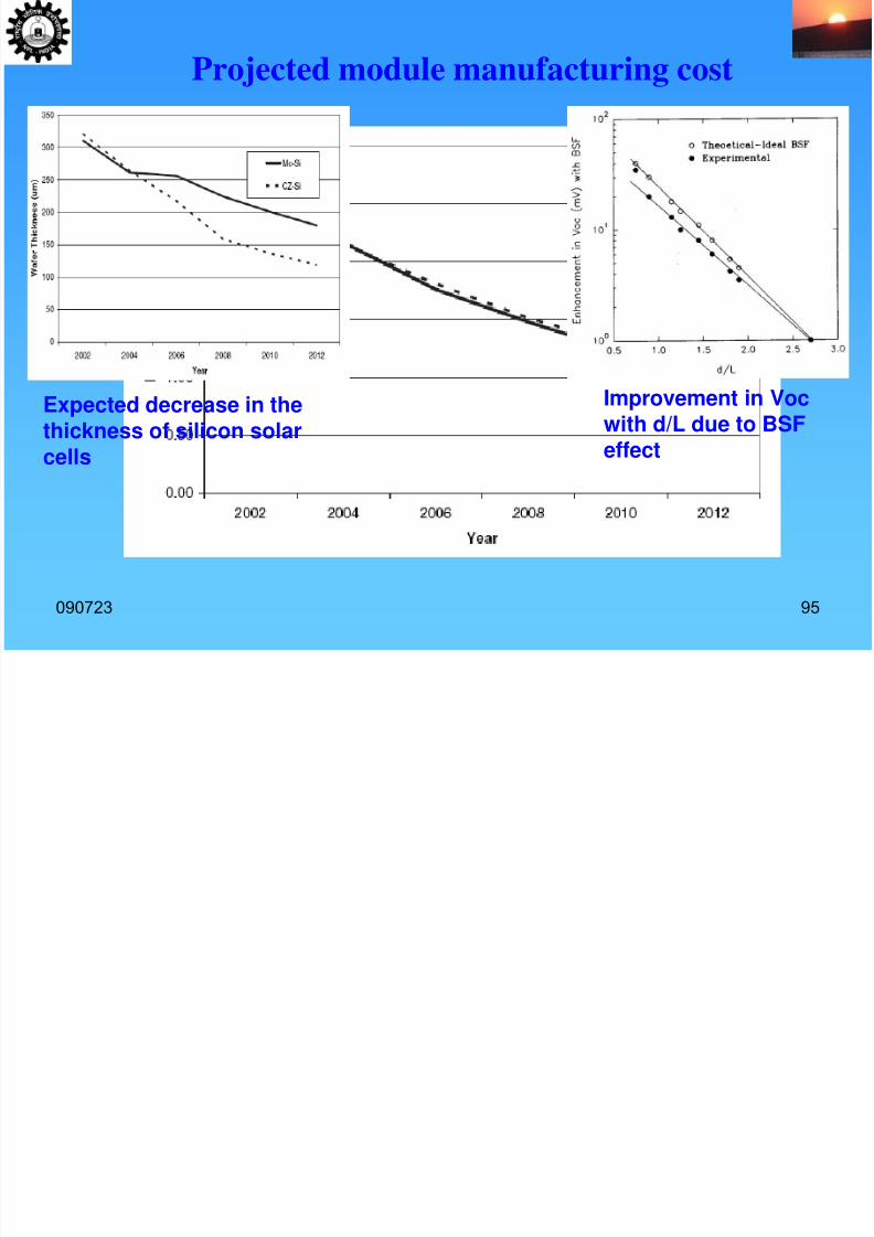
7/29/2019 perspective in photovoltaics
http://slidepdf.com/reader/full/perspective-in-photovoltaics 93/148
090723 95
Projected module manufacturing cost
Expected decrease in thethickness of silicon solarcells
Improvement in Vocwith d/L due to BSFeffect
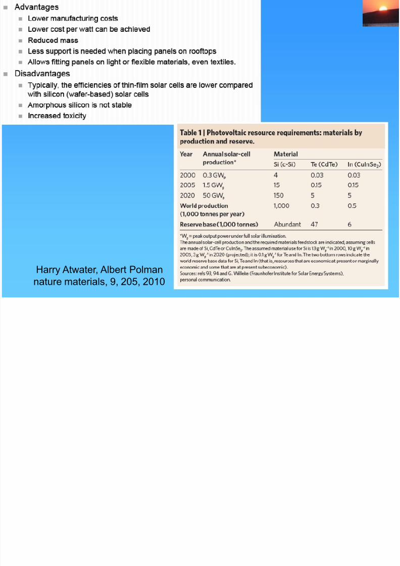
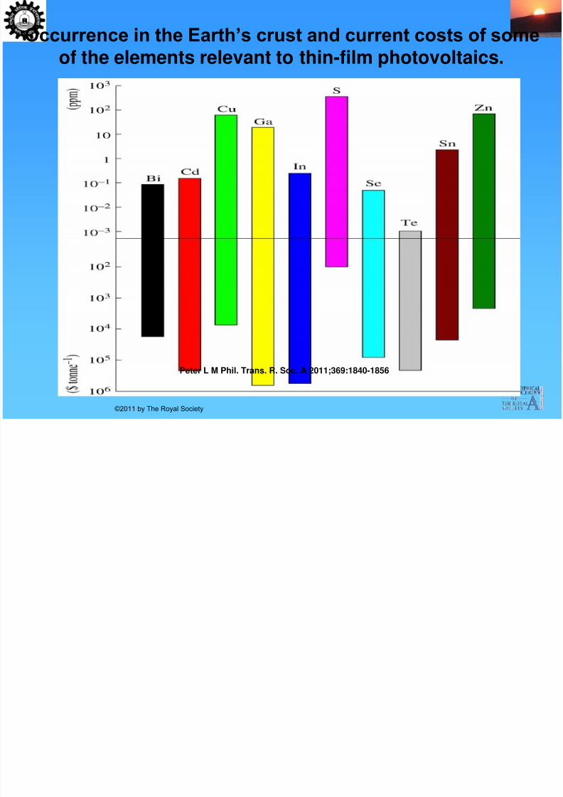
Occurrence in the Earth‟s crust and current costs of some
7/29/2019 perspective in photovoltaics
http://slidepdf.com/reader/full/perspective-in-photovoltaics 94/148
of the elements relevant to thin-film photovoltaics.
Peter L M Phil. Trans. R. Soc. A 2011;369:1840-1856
©2011 by The Royal Society
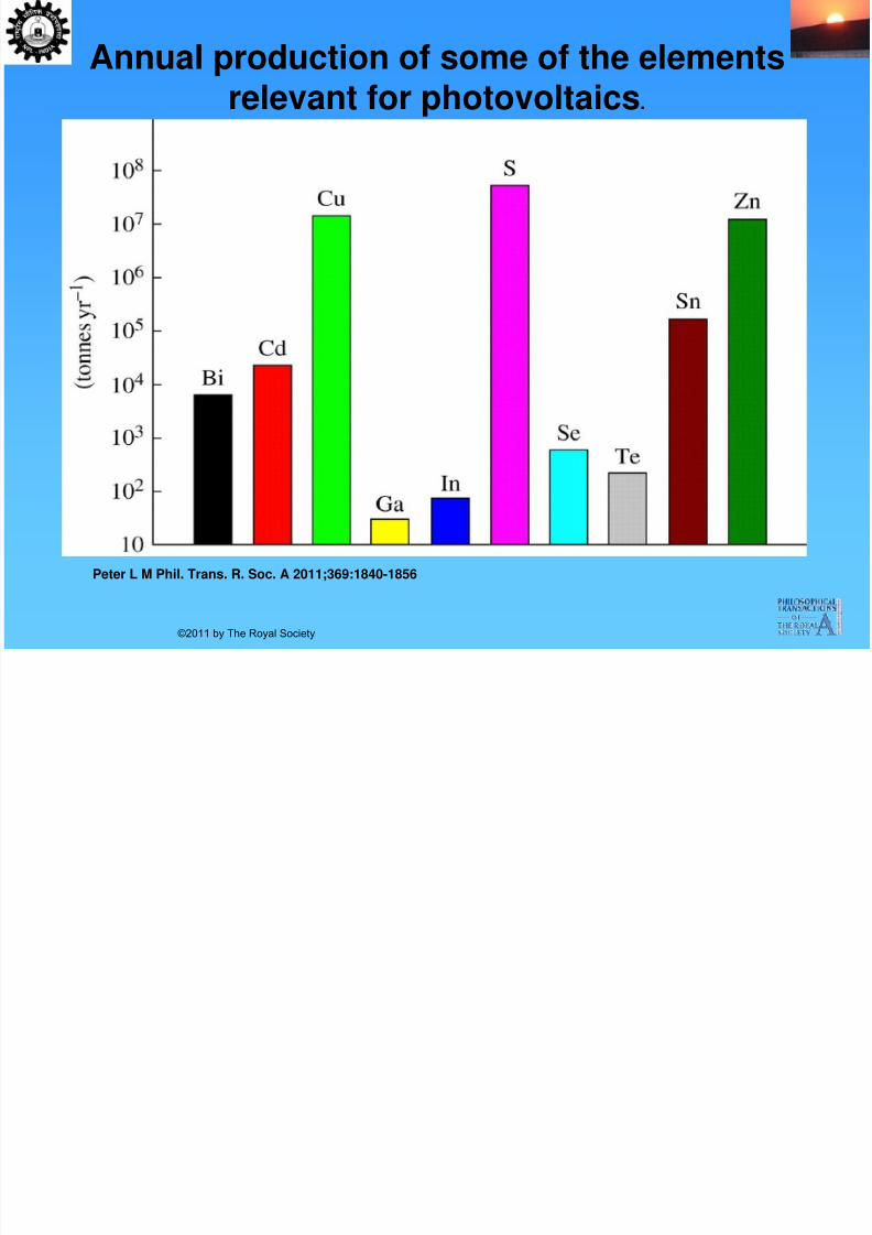
Annual production of some of the elements
7/29/2019 perspective in photovoltaics
http://slidepdf.com/reader/full/perspective-in-photovoltaics 95/148
prelevant for photovoltaics.
Peter L M Phil. Trans. R. Soc. A 2011;369:1840-1856
©2011 by The Royal Society
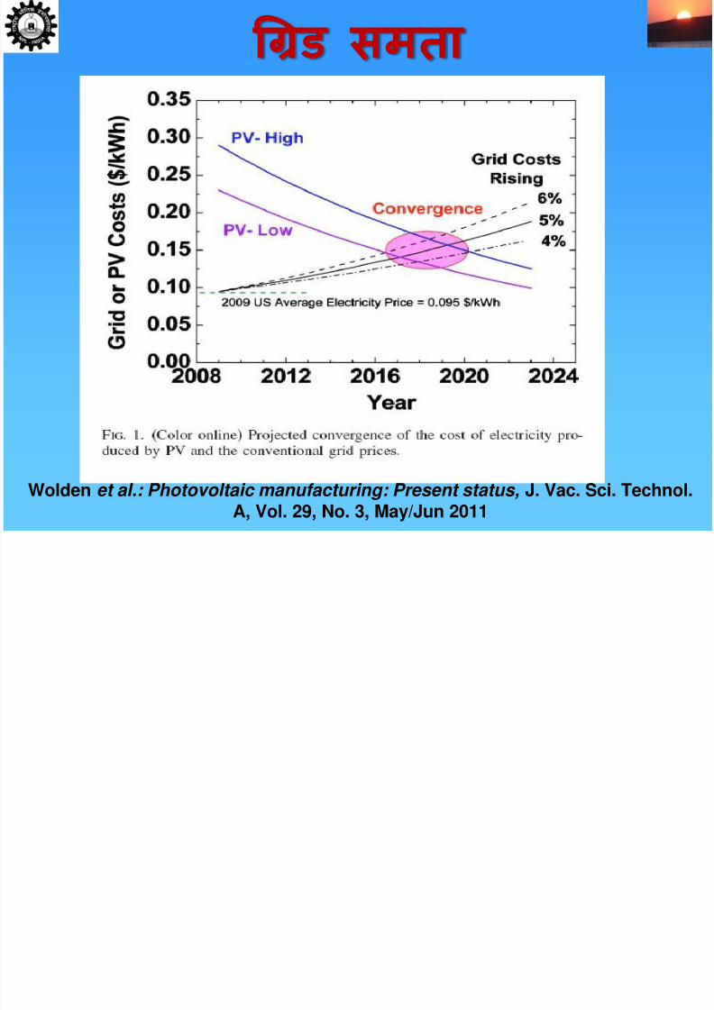
िड समतज
7/29/2019 perspective in photovoltaics
http://slidepdf.com/reader/full/perspective-in-photovoltaics 96/148
Wolden et al.: Photovoltaic manufacturing: Present status, J. Vac. Sci. Technol.
A, Vol. 29, No. 3, May/Jun 2011
7/29/2019 perspective in photovoltaics
http://slidepdf.com/reader/full/perspective-in-photovoltaics 97/148
7/29/2019 perspective in photovoltaics
http://slidepdf.com/reader/full/perspective-in-photovoltaics 98/148
7/29/2019 perspective in photovoltaics
http://slidepdf.com/reader/full/perspective-in-photovoltaics 99/148
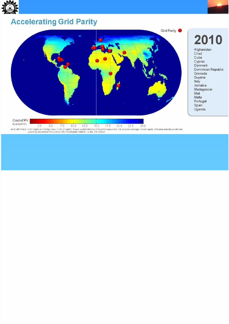
These countries represent 98% of the world population99.7% of world’s GDP and 99.2% of world’s CO2 emission
And 99.5% of residential electricity consumption
30%/yr Growth would lead to 250GW/yr in 2020
द ुनयज क क ु ऱ अधषठजऩत PV ऺमतज
7/29/2019 perspective in photovoltaics
http://slidepdf.com/reader/full/perspective-in-photovoltaics 100/148
ु ु
Peter L M Phil. Trans. R. Soc. A 2011;369:1840-1856
©2011 by The Royal Society
From bottom to top: China, USA, ROW, Japan, EU.
30 TW in 2100
7/29/2019 perspective in photovoltaics
http://slidepdf.com/reader/full/perspective-in-photovoltaics 101/148
30 TW in 2100
• sana 2100 maoM saarI ऊरात सौ फोटोवोलटक haogaI
• lagaBaga 1 TW vaaiYak ]%pad haogaa jaao ABaI ka 100 gaunaa
hO
• [sako ilayao lagaBaga 1012 va maI xao~ caaihyao (106 वगत कऱोमीट )
• भा का क ु ऱ भौगोऱक ऺे 3,287,240 वगत कऱोमीट है •
[sako ilayao bahut saamaga/I AaOr ऊरात AavaSyak haOgaI
• @yaa yah hao payaogaa
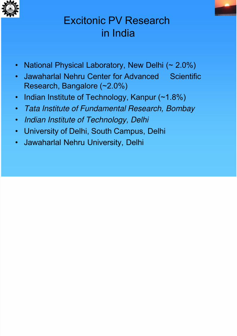
Excitonic PV Research
7/29/2019 perspective in photovoltaics
http://slidepdf.com/reader/full/perspective-in-photovoltaics 102/148
Excitonic PV Researchin India
• National Physical Laboratory, New Delhi (~ 2.0%)
• Jawaharlal Nehru Center for Advanced Scientific
Research, Bangalore (~2.0%)• Indian Institute of Technology, Kanpur (~1.8%)
• Tata Institute of Fundamental Research, Bombay
• Indian Institute of Technology, Delhi
• University of Delhi, South Campus, Delhi• Jawaharlal Nehru University, Delhi
7/29/2019 perspective in photovoltaics
http://slidepdf.com/reader/full/perspective-in-photovoltaics 103/148
िवा कने बा
7/29/2019 perspective in photovoltaics
http://slidepdf.com/reader/full/perspective-in-photovoltaics 104/148
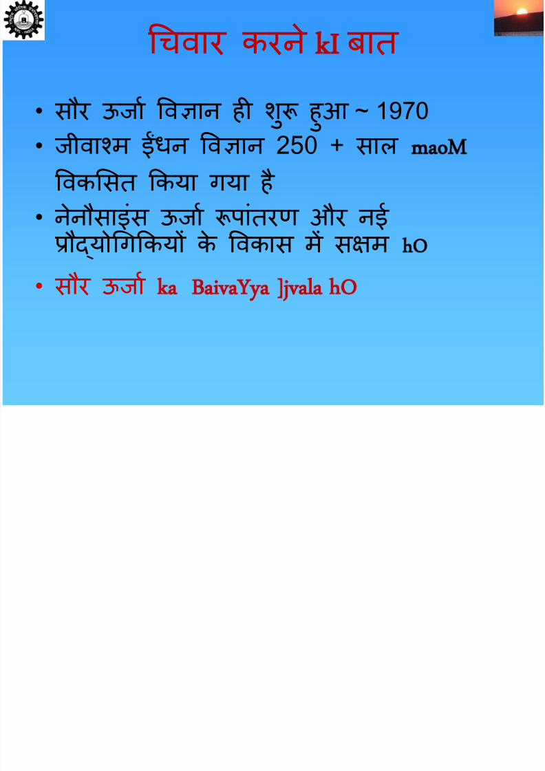
िवा कन बा
• सौ ऊरात वऻान ह श ु ह ुआ ~ 1970 • रीवाम न वऻान 250 + साऱ
वकस कया गया है • नेनौसाइॊस ऊरात पाॊण औ नई ौयोचगकय के वकास म सऺम
• सौ ऊरात
7/29/2019 perspective in photovoltaics
http://slidepdf.com/reader/full/perspective-in-photovoltaics 105/148
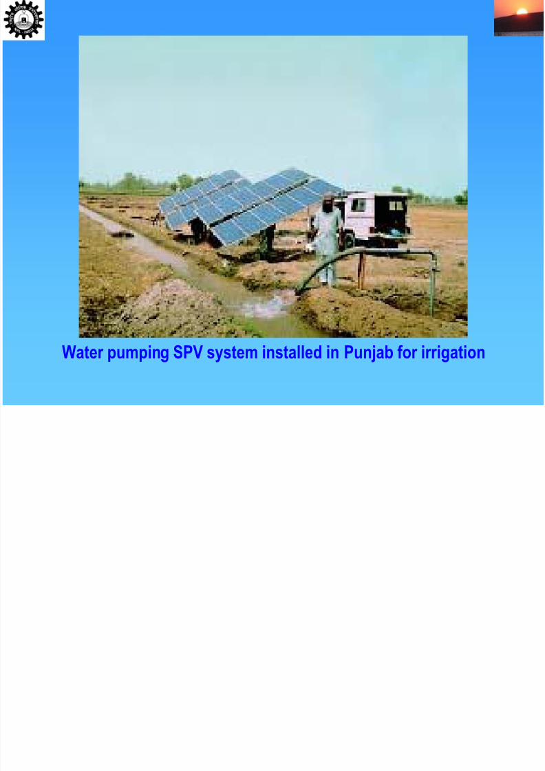
Water pumping SPV system installed in Punjab for irrigation
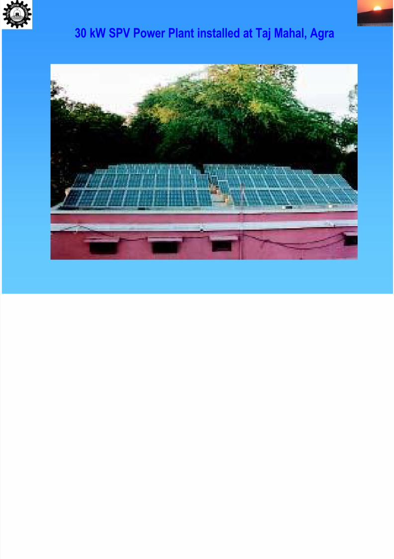
30 kW SPV Power Plant installed at Taj Mahal, Agra
7/29/2019 perspective in photovoltaics
http://slidepdf.com/reader/full/perspective-in-photovoltaics 106/148
j , g
7/29/2019 perspective in photovoltaics
http://slidepdf.com/reader/full/perspective-in-photovoltaics 107/148
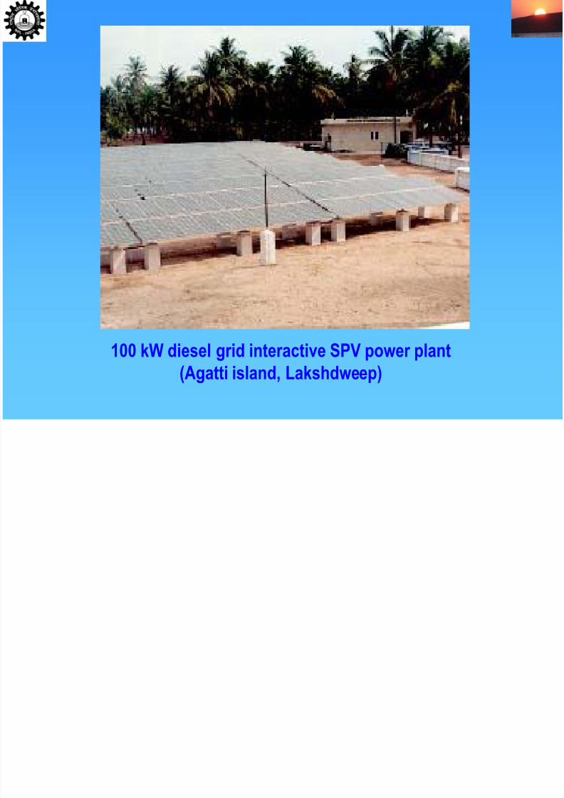
100 kW diesel grid interactive SPV power plant (Agatti island, Lakshdweep)
7/29/2019 perspective in photovoltaics
http://slidepdf.com/reader/full/perspective-in-photovoltaics 108/148
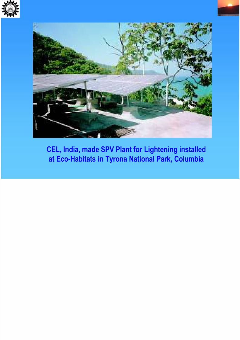
CEL, India, made SPV Plant for Lightening installed
at Eco-Habitats in Tyrona National Park, Columbia
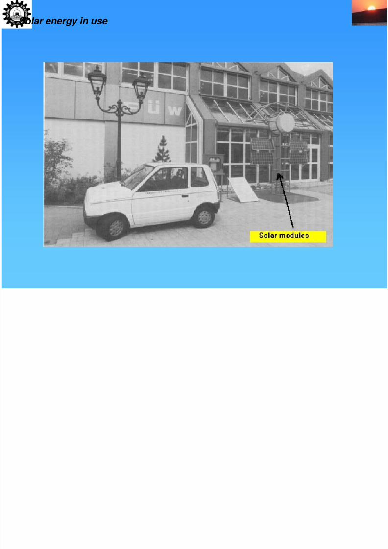
Solar energy in use
7/29/2019 perspective in photovoltaics
http://slidepdf.com/reader/full/perspective-in-photovoltaics 109/148
7/29/2019 perspective in photovoltaics
http://slidepdf.com/reader/full/perspective-in-photovoltaics 110/148
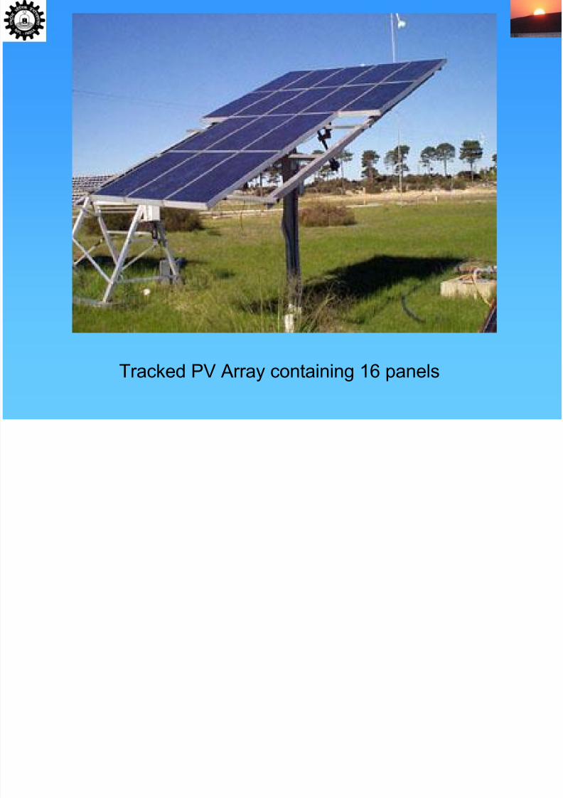
Tracked PV Array containing 16 panels
7/29/2019 perspective in photovoltaics
http://slidepdf.com/reader/full/perspective-in-photovoltaics 111/148
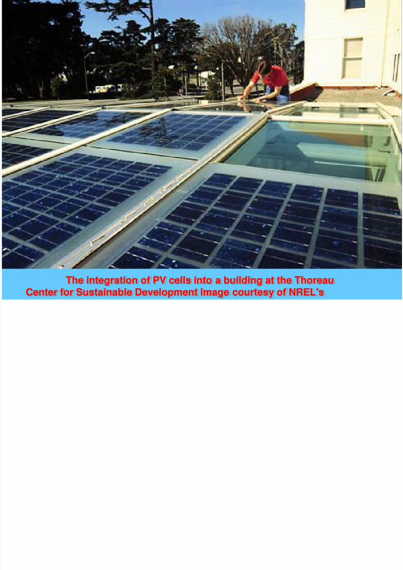
The integration of PV cells into a building at the Thoreau
Center for Sustainable Development Image courtesy of NREL's
7/29/2019 perspective in photovoltaics
http://slidepdf.com/reader/full/perspective-in-photovoltaics 112/148
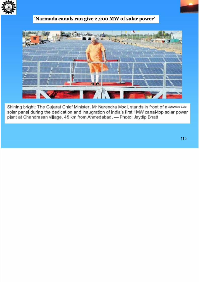
115
7/29/2019 perspective in photovoltaics
http://slidepdf.com/reader/full/perspective-in-photovoltaics 113/148
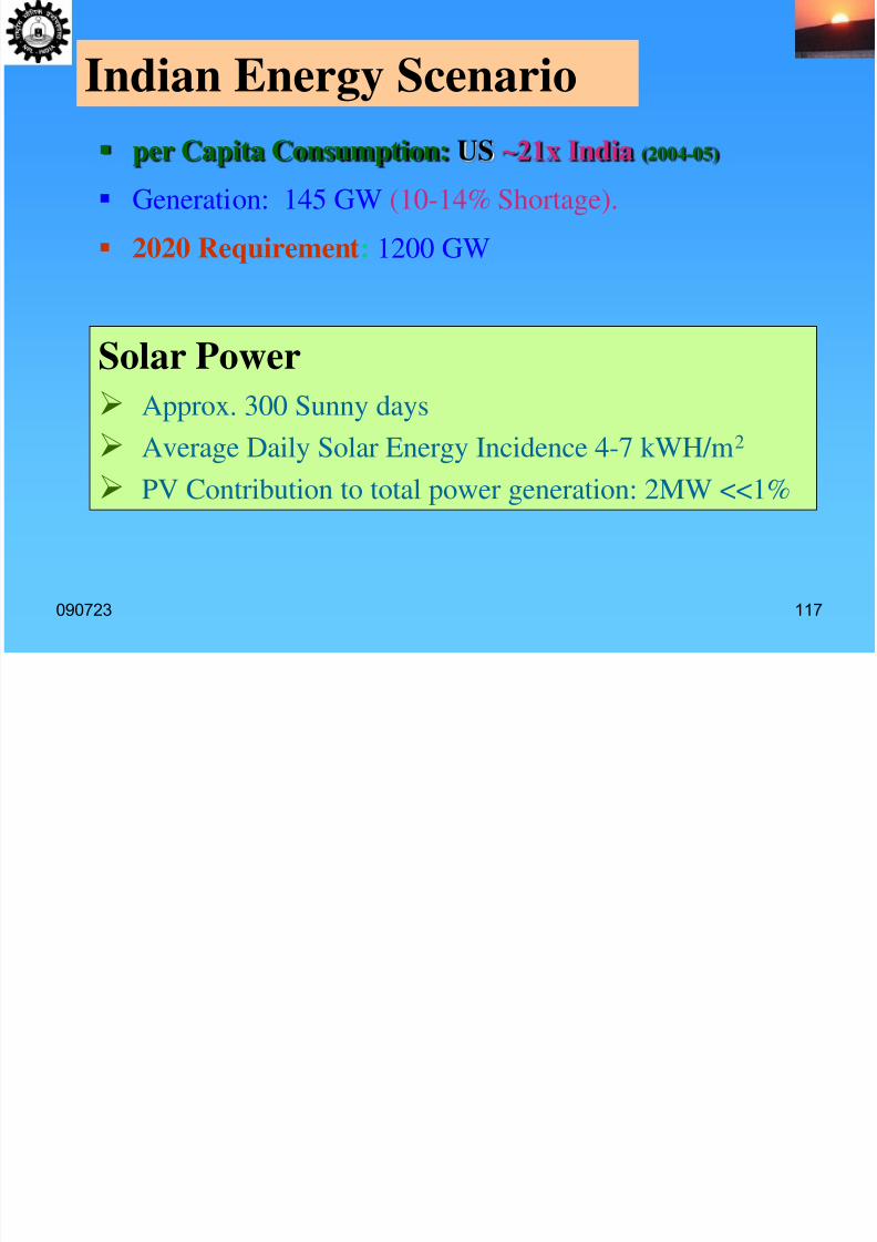
Indian Energy Scenario
7/29/2019 perspective in photovoltaics
http://slidepdf.com/reader/full/perspective-in-photovoltaics 114/148
090723 117
Solar Power
Approx. 300 Sunny days
Average Daily Solar Energy Incidence 4-7 kWH/m2
PV Contribution to total power generation: 2MW <<1%
per Capita Consumption: US ~21x India (2004-05)
Generation: 145 GW (10-14% Shortage).
2020 Requirement: 1200 GW
d a e gy Sce a o

7/29/2019 perspective in photovoltaics
http://slidepdf.com/reader/full/perspective-in-photovoltaics 115/148
श ुया

7/29/2019 perspective in photovoltaics
http://slidepdf.com/reader/full/perspective-in-photovoltaics 116/148
I thank numerous persons who havecontributed to this presentation
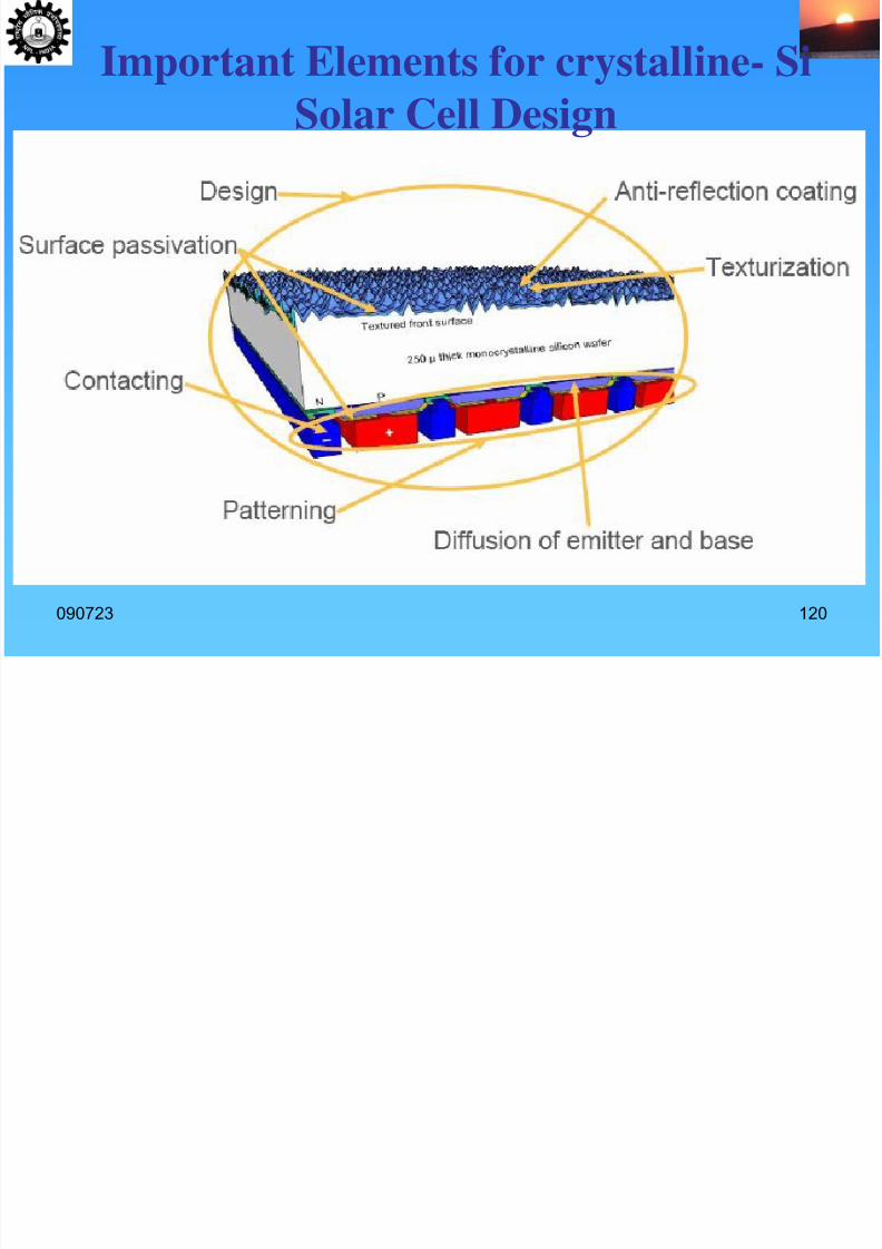
Important Elements for crystalline- Si
7/29/2019 perspective in photovoltaics
http://slidepdf.com/reader/full/perspective-in-photovoltaics 117/148
090723 120
Solar Cell Design
7/29/2019 perspective in photovoltaics
http://slidepdf.com/reader/full/perspective-in-photovoltaics 118/148
090723 121121
PV Production: Global & India 4000
7/29/2019 perspective in photovoltaics
http://slidepdf.com/reader/full/perspective-in-photovoltaics 119/148
090723 122
2008 PV ShipmentInternational : ~5.95 GWIndian : ~150 MW
Cumulative Installation~18 GW: 1/1000th Energy Portfolio
Projected PV Production2010 : 14 GW
2030: 140 GW
1975 1980 1985 1990 1995 2000 20050
500
1000
1500
2000
2500
3000
3500
4000
A n n u a l P V P r o d u c t i o n ( M W )
Year
Compound Annual Growth 44%
2002-07
2006 2007-8 2008-9 2010BP Solar 13 36 85-128
Webel 8 100*Maharshi 5 15CEL 3 12BHEL 2 10Maharshi * 8 15Others 1
MBPV 80 200 750Signet Solar 300Solar Semiconductor 60 220HHV 15
Future InvestmentsSignet Solar (3*300MW) -10yrsReliance and 10 more US$ 5-6b Investment,Special Incentive Package Scheme 18b
USD
E i C
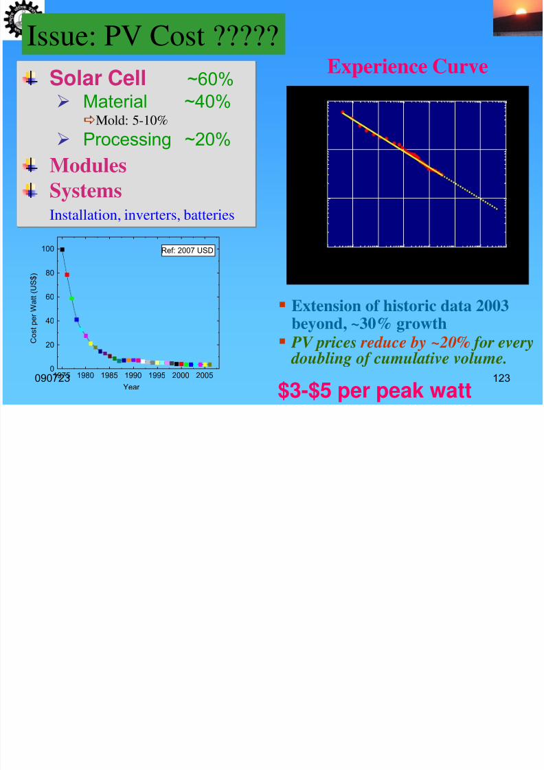
Issue: PV Cost ?????
7/29/2019 perspective in photovoltaics
http://slidepdf.com/reader/full/perspective-in-photovoltaics 120/148
090723 123
Solar Cell ~60%
Material ~40%Mold: 5-10%
Processing ~20%
Modules
SystemsInstallation, inverters, batteries
$3-$5 per peak watt
Experience Curve
10-1
100
101
102
103
104
105
106
10-1
10
0
101
102
Cumulative Production (MWp)
M o d u l e C o s t ( 2 0 0 3 $ / W
p
)
Extension of historic data 2003beyond, ~30% growth
PV prices reduce by ~20% for every doubling of cumulative volume.
1975 1980 1985 1990 1995 2000 20050
20
40
60
80
100
C o s t p e r W a t t ( U S $ )
Year
Ref: 2007 USD
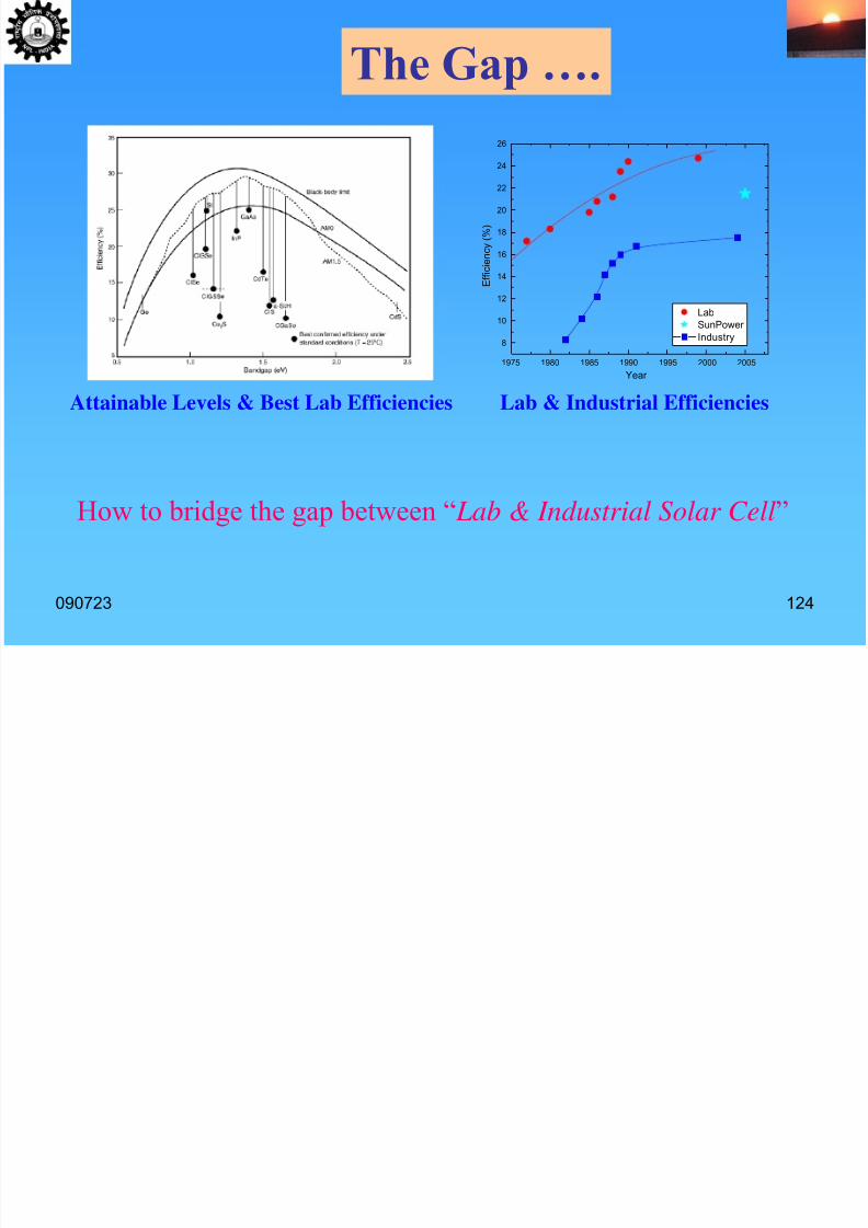
The Gap ….
7/29/2019 perspective in photovoltaics
http://slidepdf.com/reader/full/perspective-in-photovoltaics 121/148
090723 124
1975 1980 1985 1990 1995 2000 2005
8
10
12
14
16
18
20
22
24
26
E f f i c i e n c y ( % )
Year
Lab
SunPower Industry
Attainable Levels & Best Lab Efficiencies Lab & Industrial Efficiencies
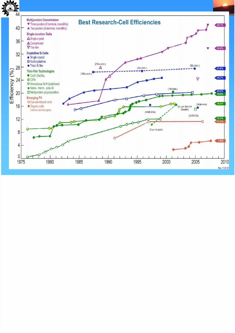
How to bridge the gap between “ Lab & Industrial Solar Cell”
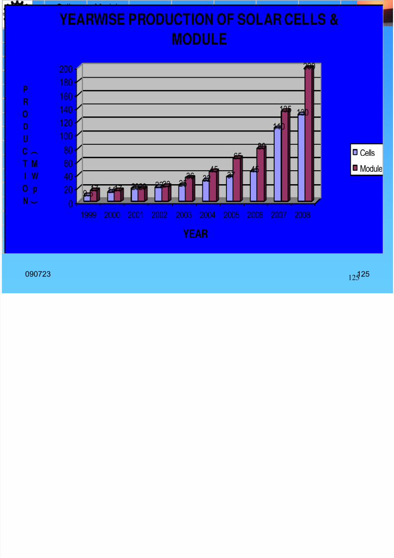
Year Cells Module1999 9.5 17
2000 14 17
YEARWISE PRODUCTION OF SOLAR CELLS &
MODULE
7/29/2019 perspective in photovoltaics
http://slidepdf.com/reader/full/perspective-in-photovoltaics 122/148
090723 125125
2001 20 20
2002 22 23
2003 25 362004 32 45
2005 37 65
2006 45 80
2007 110 135
2008 130 200
9.517 1417 2020 2223 25
36 32
4537
65
45
80
110
135 130
200
0
20
40
60
80
100
120
140
160
180
200
P
R
O
D
U
C
T
I
O
N
(
M
W
p )
1999 2000 2001 2002 2003 2004 2005 2006 2007 2008
YEAR
MODULE
Cells
Module
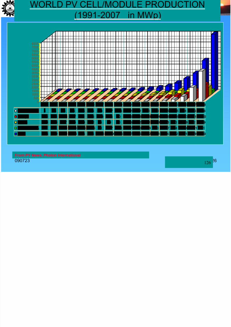
WORLD PV CELL/MODULE PRODUCTION(1991-2007 in MWp)
7/29/2019 perspective in photovoltaics
http://slidepdf.com/reader/full/perspective-in-photovoltaics 123/148
090723 126126
0500
100015002000
250030003500400045005000550060006500700075008000
Rest of World 5 4.6 4.4 5.6 6.35 9.75 9.4 18.7 20.5 23.42 32.62 47.8 83.8 141.5 322.5 714 1943 4188
Europe 13.4 16.4 16.55 21.7 20.1 18.8 30.4 33.5 40 60.66 86.38 112.8 193.4 311.8 476.6 678.3 1171 2020
Japan 19.9 18.8 16.7 16.5 16.4 21.2 35 49 80 128.6 171.2 251.1 363.9 601.5 833 926.9 932 1269
United States 17.1 18.1 22.44 25.64 34.75 38.85 51 53.7 60.8 74.97 100.3 100.6 103 138.7 154 201.6 233.1 431
Total 55.4 57.9 60.09 69.44 77.6 88.6 125.8 154.9 201.3 287.7 390.5 512.2 744.1 1194 1782 2521 4279 7910
1991 1992 1993 1994 1995 1996 1997 1998 1999 2000 2001 2002 2003 2004 2005 2006 2007 2008
From PV News, Photon International
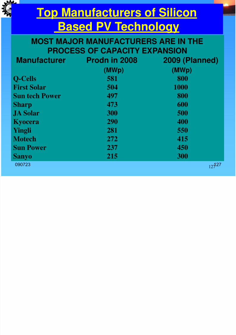
Top Manufacturers of SiliconBased PV Technology
7/29/2019 perspective in photovoltaics
http://slidepdf.com/reader/full/perspective-in-photovoltaics 124/148
090723 127127
MOST MAJOR MANUFACTURERS ARE IN THEPROCESS OF CAPACITY EXPANSION
Manufacturer Prodn in 2008 2009 (Planned)(MWp) (MWp)
Q-Cells 581 800
First Solar 504 1000Sun tech Power 497 800
Sharp 473 600
JA Solar 300 500
Kyocera 290 400
Yingli 281 550Motech 272 415
Sun Power 237 450
Sanyo 215 300
Based PV Technology
7/29/2019 perspective in photovoltaics
http://slidepdf.com/reader/full/perspective-in-photovoltaics 125/148
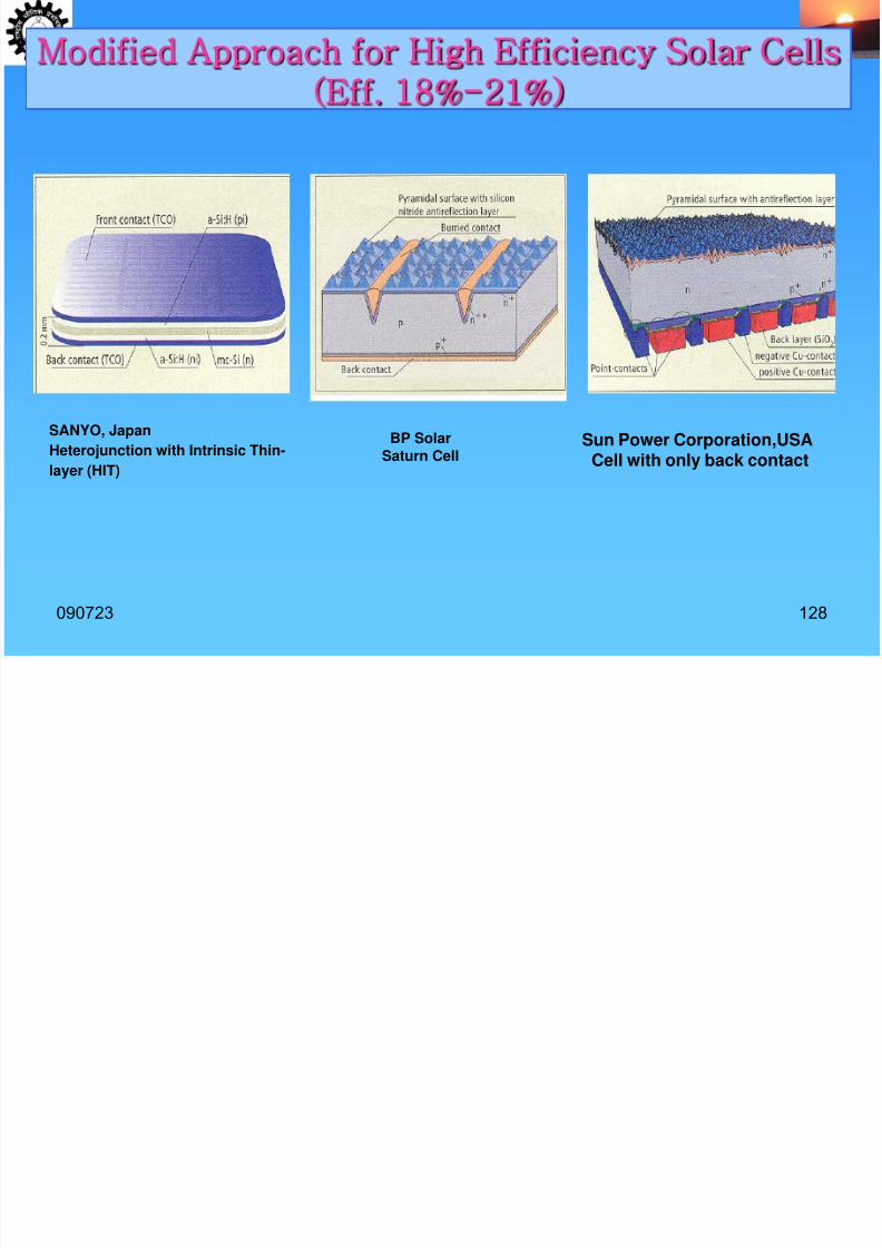
090723 128
SANYO, Japan
Heterojunction with Intrinsic Thin-
layer (HIT)
BP SolarSaturn Cell
Sun Power Corporation,USACell with only back contact
7/29/2019 perspective in photovoltaics
http://slidepdf.com/reader/full/perspective-in-photovoltaics 126/148
090723 129
New Silicon Plants
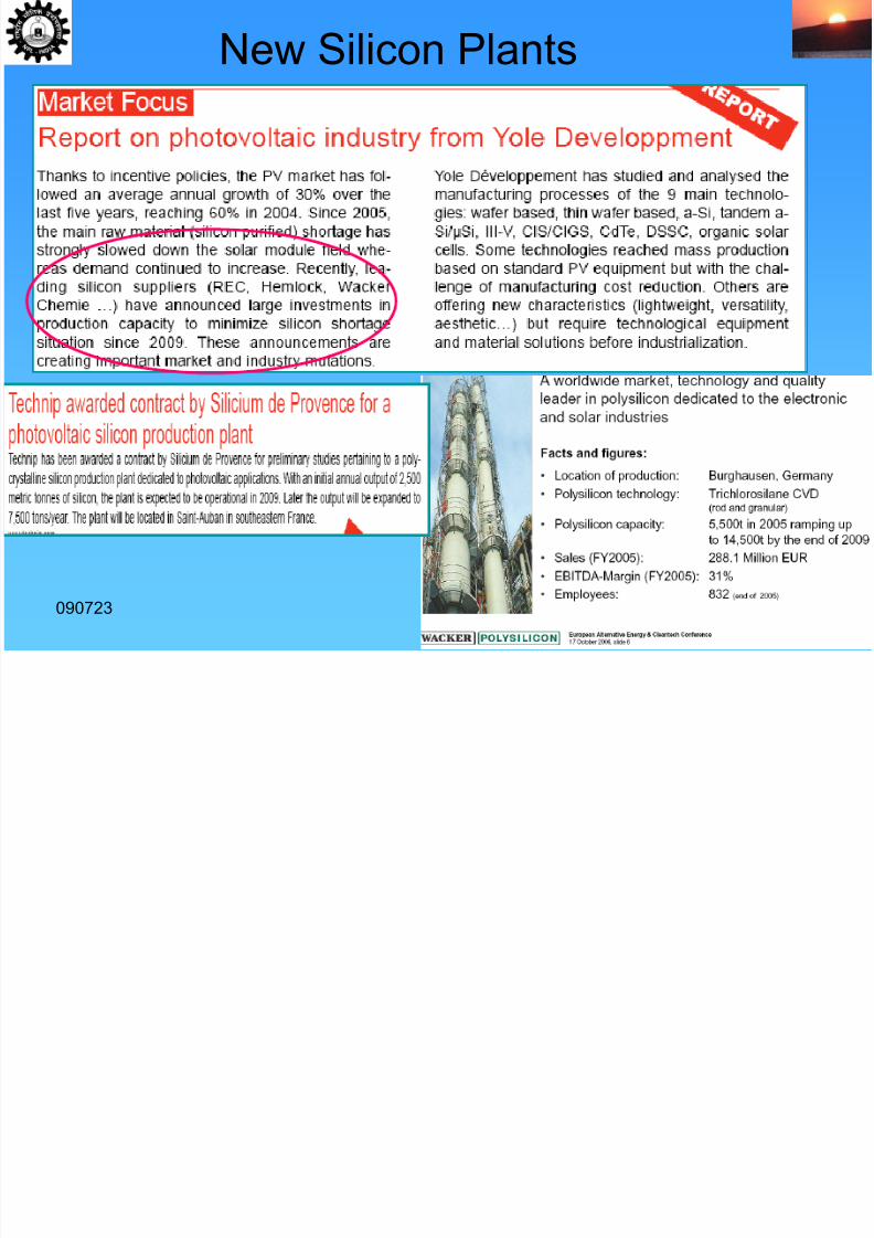
7/29/2019 perspective in photovoltaics
http://slidepdf.com/reader/full/perspective-in-photovoltaics 127/148
090723 130
7/29/2019 perspective in photovoltaics
http://slidepdf.com/reader/full/perspective-in-photovoltaics 128/148
090723 131
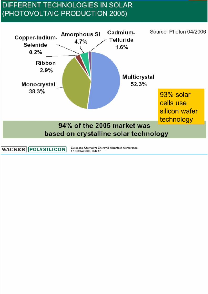
93% solar cells use
silicon wafer technology
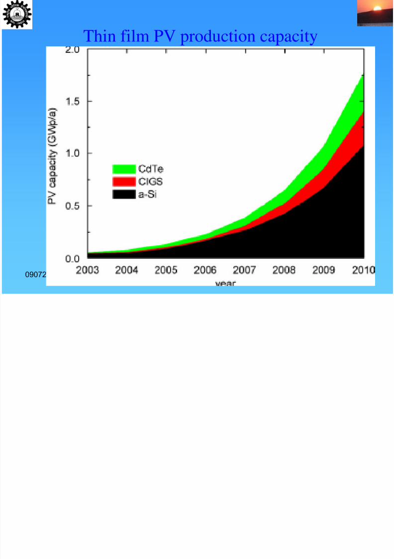
Thin film PV production capacity
7/29/2019 perspective in photovoltaics
http://slidepdf.com/reader/full/perspective-in-photovoltaics 129/148
090723 132
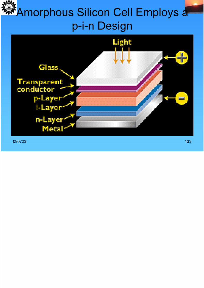
Amorphous Silicon Cell Employs ap i n Design
7/29/2019 perspective in photovoltaics
http://slidepdf.com/reader/full/perspective-in-photovoltaics 130/148
090723 133
p-i-n Design
M t l C t t
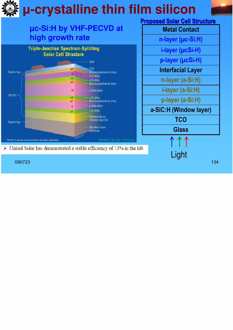
Proposed Solar Cell Structure µc Si:H by VHF PECVD at
μ-crystalline thin film silicon
7/29/2019 perspective in photovoltaics
http://slidepdf.com/reader/full/perspective-in-photovoltaics 131/148
090723 134
Metal Contact
n-layer (µc-Si:H)
i-layer (µcSi-H)
p-layer (µcSi-H)
Interfacial Layer
n-layer (a-Si:H)
i-layer (a-Si:H)
p-layer (a-Si:H)
a-SiC:H (Window layer)
TCO
Glass
Light
µc-Si:H by VHF-PECVD athigh growth rate
Hetrojunction with Intrinsic Thin Layer
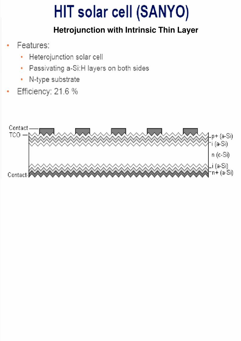
7/29/2019 perspective in photovoltaics
http://slidepdf.com/reader/full/perspective-in-photovoltaics 132/148
090723 135
Hetrojunction with Intrinsic Thin Layer
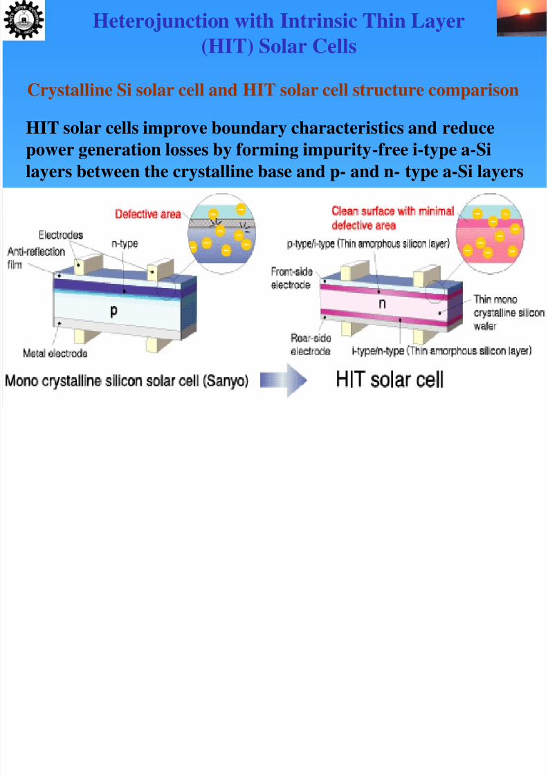
7/29/2019 perspective in photovoltaics
http://slidepdf.com/reader/full/perspective-in-photovoltaics 133/148
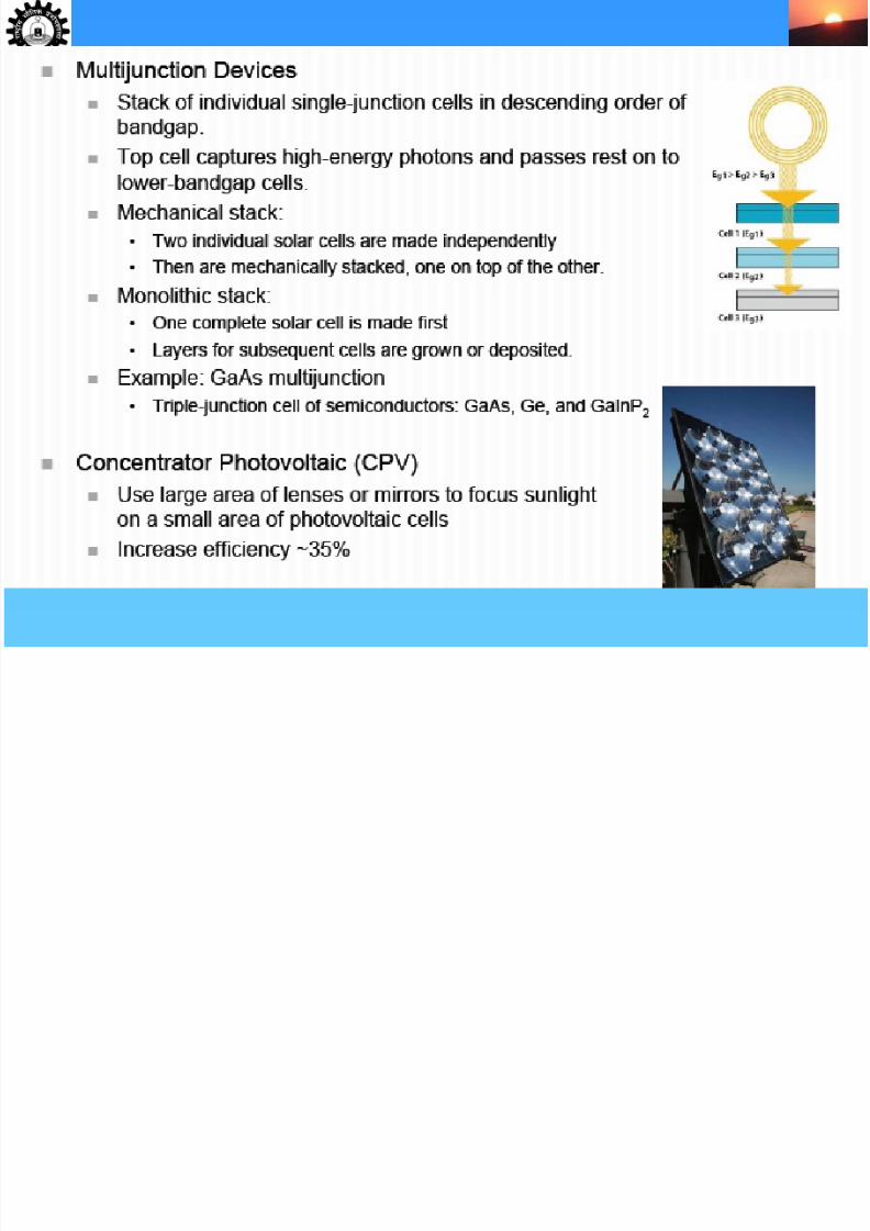
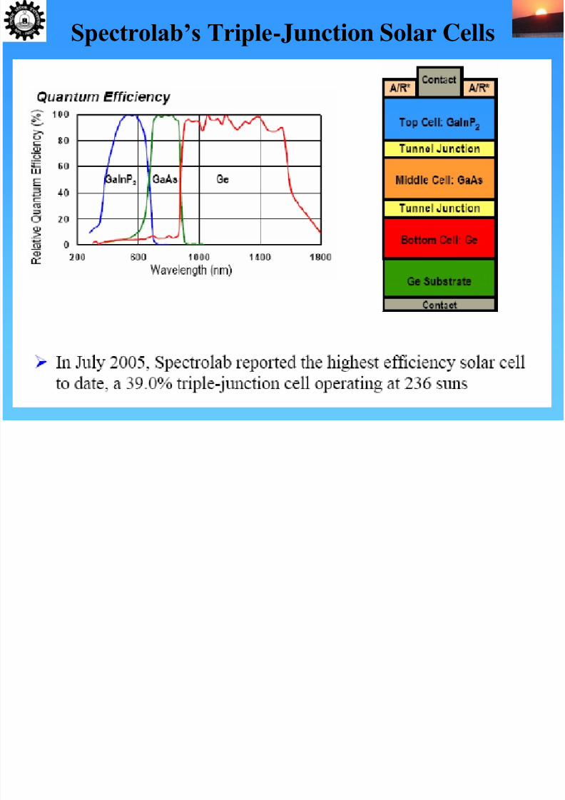
Spectrolab’s Triple-Junction Solar Cells
7/29/2019 perspective in photovoltaics
http://slidepdf.com/reader/full/perspective-in-photovoltaics 134/148
090723 137
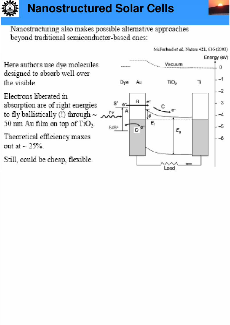
Nanostructured Solar Cells
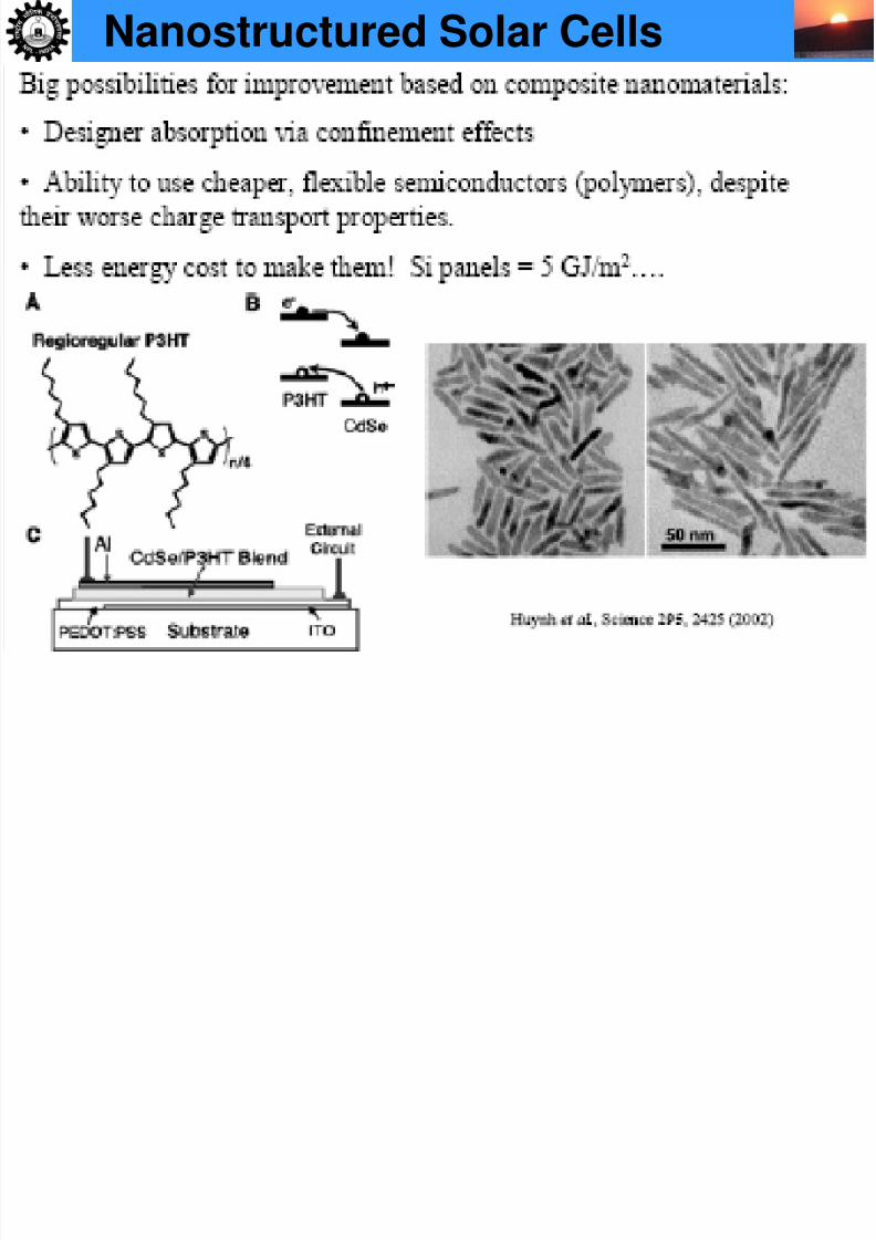
7/29/2019 perspective in photovoltaics
http://slidepdf.com/reader/full/perspective-in-photovoltaics 135/148
090723 138
Nanostructured Solar Cells
7/29/2019 perspective in photovoltaics
http://slidepdf.com/reader/full/perspective-in-photovoltaics 136/148
090723 139
7/29/2019 perspective in photovoltaics
http://slidepdf.com/reader/full/perspective-in-photovoltaics 137/148
090723 140
J V Fill (%) Peak QE &
Current status of various solar cells
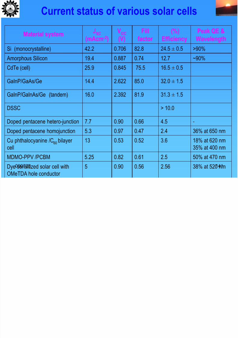
7/29/2019 perspective in photovoltaics
http://slidepdf.com/reader/full/perspective-in-photovoltaics 138/148
090723 141
Material system JSC
(mAcm-2) VOC
(V)
Fill
factor
(%)
Efficiency Peak QE &
Wavelength
Si (monocrystalline) 42.2 0.706 82.8 24.5 ± 0.5 >90% Amorphous Silicon 19.4 0.887 0.74 12.7 ~90%
CdTe (cell) 25.9 0.845 75.5 16.5 ± 0.5
GaInP/GaAs/Ge 14.4 2.622 85.0 32.0 ± 1.5
GaInP/GaInAs/Ge (tandem) 16.0 2.392 81.9 31.3 ± 1.5
DSSC > 10.0
Doped pentacene hetero-junction 7.7 0.90 0.66 4.5 -
Doped pentacene homojunction 5.3 0.97 0.47 2.4 36% at 650 nm Cu phthalocyanine /C60 bilayer
cell 13 0.53 0.52 3.6 18% at 620 nm
35% at 400 nm
MDMO-PPV /PCBM 5.25 0.82 0.61 2.5 50% at 470 nm
Dye sensitized solar cell with
OMeTDA hole conductor
5 0.90 0.56 2.56 38% at 520 nm
Best cell efficiencies
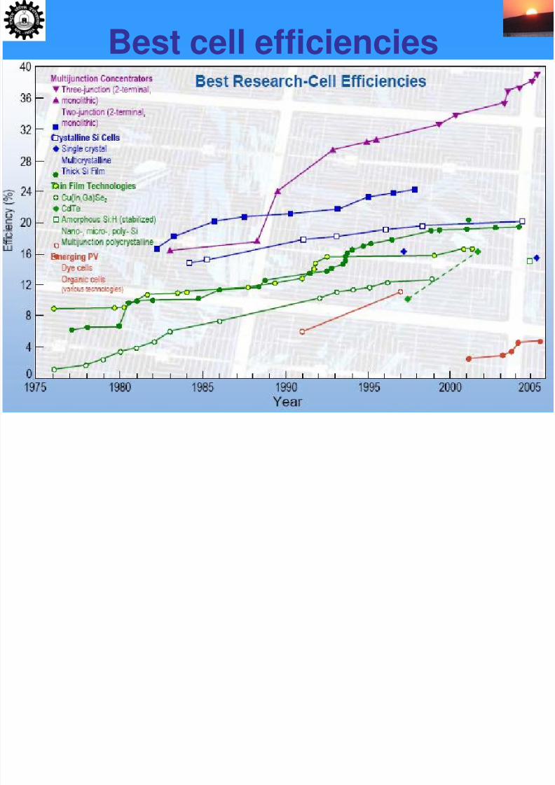
7/29/2019 perspective in photovoltaics
http://slidepdf.com/reader/full/perspective-in-photovoltaics 139/148
090723 142
PV Scenario in India
7/29/2019 perspective in photovoltaics
http://slidepdf.com/reader/full/perspective-in-photovoltaics 140/148
090723 144
• ~100 MW production – largest is Tata BPSolar with about 25 MW
• Expansion plans for all in the range of 20
to 40 MW• New players – Moser Baer PV to go up to
400 MW in 5 years. MBPV investing in a-
Si plant
R&D on Photovoltaics at NPLCrystalline Silicon: c- & mc-Si Cells (High & Industrial) >16%
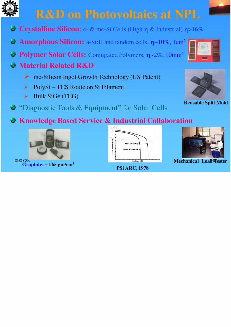
7/29/2019 perspective in photovoltaics
http://slidepdf.com/reader/full/perspective-in-photovoltaics 141/148
090723 145
Crystalline Silicon: c- & mc-Si Cells (High & Industrial) >16%
Amorphous Silicon: a-Si:H and tandem cells, ~10%, 1cm2
Polymer Solar Cells: Conjugated Polymers, ~2%, 10mm2
Material Related R&D
mc-Silicon Ingot Growth Technology (US Patent)
PolySi – TCS Route on Si Filament Bulk SiGe (TEG)
“Diagnostic Tools & Equipment” for Solar Cells
Knowledge Based Service & Industrial Collaboration
Mechanical Load Tester
Reusable Split Mold
PSi ARC, 1978Graphite: ~1.65 gm/cm3
Crystalline Si cells:
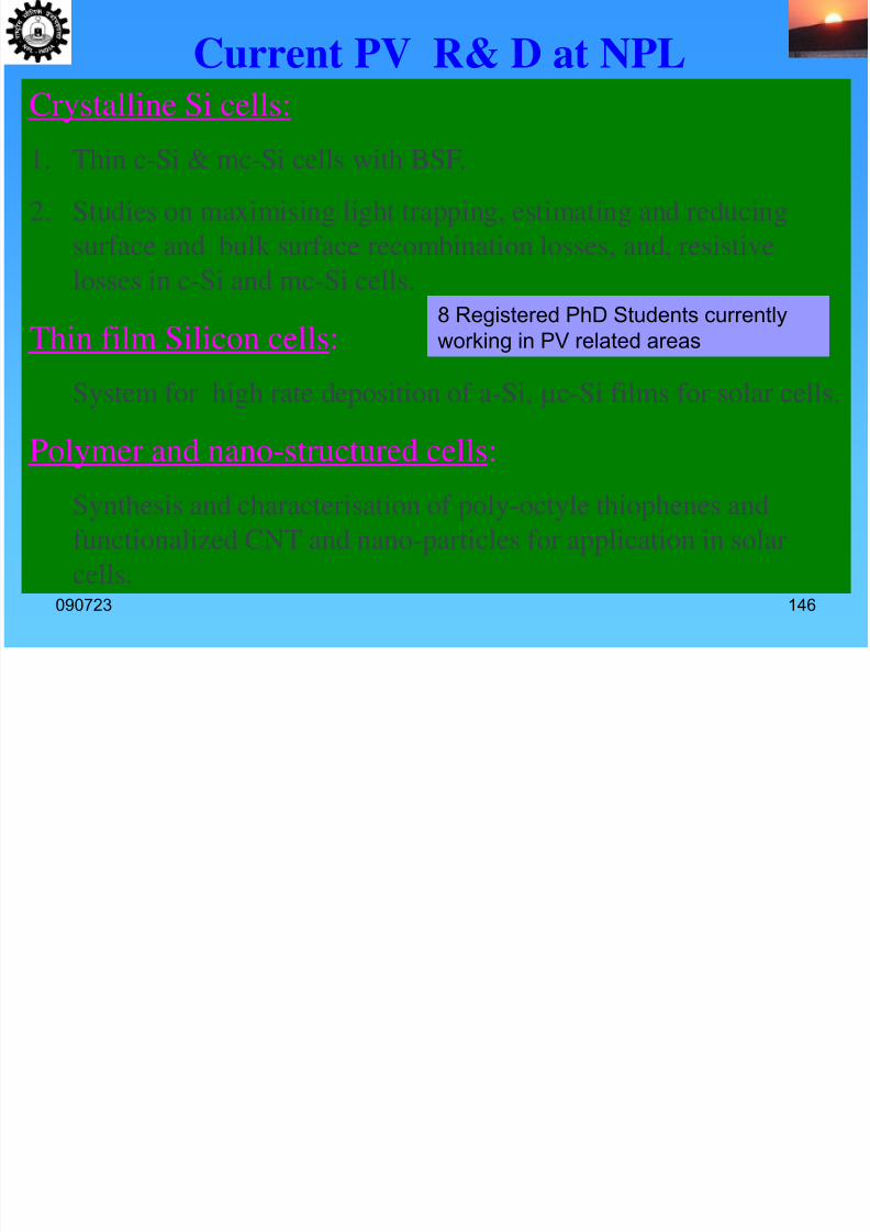
Current PV R& D at NPL
7/29/2019 perspective in photovoltaics
http://slidepdf.com/reader/full/perspective-in-photovoltaics 142/148
090723 146
Crystalline Si cells:
1. Thin c-Si & mc-Si cells with BSF.
2. Studies on maximising light trapping, estimating and reducing
surface and bulk surface recombination losses, and, resistive
losses in c-Si and mc-Si cells.
Thin film Silicon cells:
System for high rate deposition of a-Si, c-Si films for solar cells.
Polymer and nano-structured cells:
Synthesis and characterisation of poly-octyle thiophenes and
functionalized CNT and nano-particles for application in solar
cells.
8 Registered PhD Students currentlyworking in PV related areas
Summary
7/29/2019 perspective in photovoltaics
http://slidepdf.com/reader/full/perspective-in-photovoltaics 143/148
090723 147
• The PV Scenario around the world is likelyto be dominated by bulk Si technology withcon tinuous improvements
• Thin Si film technologies will gain.• New structures based polymers and
nanostructures need a breakthrough
• NPL will increase the solar energy effortsin coming years
7/29/2019 perspective in photovoltaics
http://slidepdf.com/reader/full/perspective-in-photovoltaics 144/148
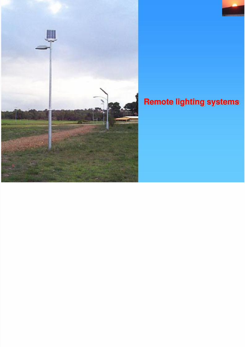
Remote lighting systems
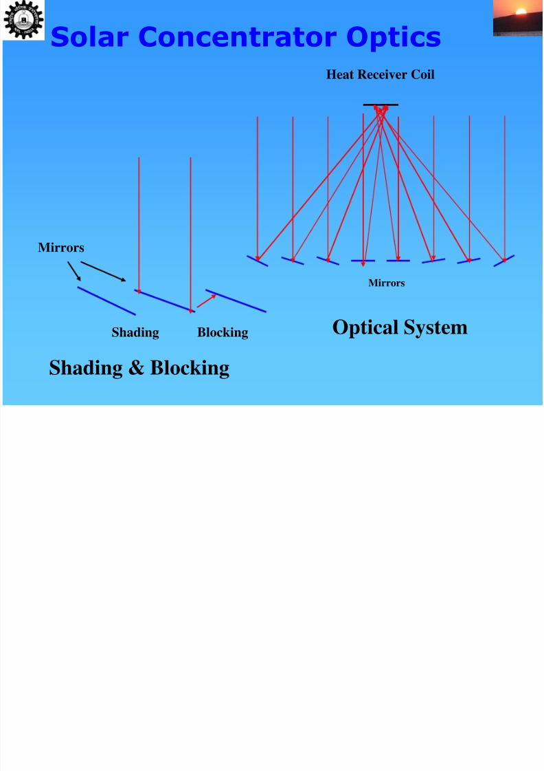
Heat Receiver Coil
Solar Concentrator Optics
7/29/2019 perspective in photovoltaics
http://slidepdf.com/reader/full/perspective-in-photovoltaics 145/148
Heat Receiver Coil
Mirrors
Optical SystemShading Blocking
Mirrors
Shading & Blocking
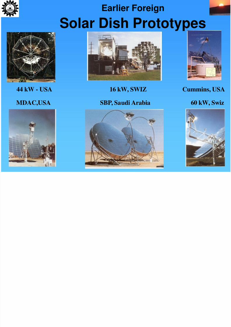
Earlier Foreign Solar Dish Prototypes
7/29/2019 perspective in photovoltaics
http://slidepdf.com/reader/full/perspective-in-photovoltaics 146/148
44 kW - USA
SBP, Saudi ArabiaMDAC,USA
16 kW, SWIZ
60 kW, Swiz
Cummins, USA
7/29/2019 perspective in photovoltaics
http://slidepdf.com/reader/full/perspective-in-photovoltaics 147/148
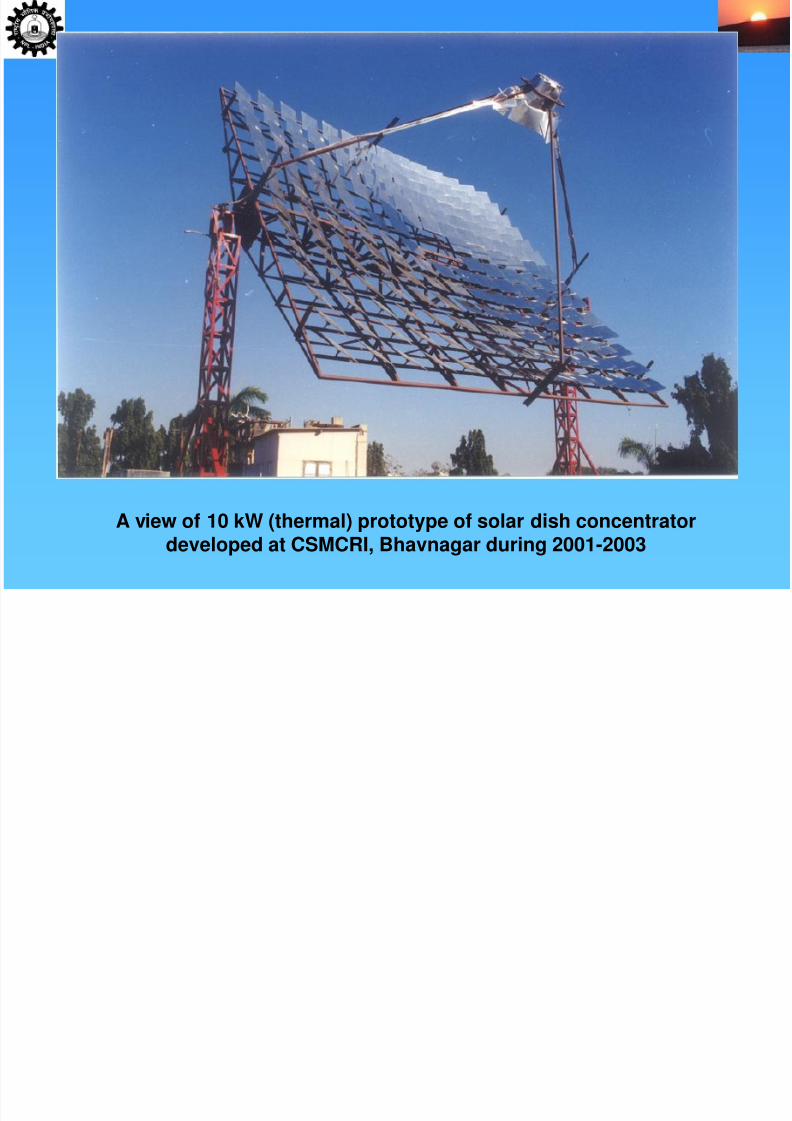
A view of 10 kW (thermal) prototype of solar dish concentratordeveloped at CSMCRI, Bhavnagar during 2001-2003
7/29/2019 perspective in photovoltaics
http://slidepdf.com/reader/full/perspective-in-photovoltaics 148/148
Thank you
Thank you for your attention