
PersonalScope HPS40 Technical Doc - Velleman tech doc screen.pdf · HPS40 Technical Doc Packaging...
20
PersonalScope PersonalScope PersonalScope PersonalScope HPS40 Technical Doc 28/10/2002 ©
Transcript of PersonalScope HPS40 Technical Doc - Velleman tech doc screen.pdf · HPS40 Technical Doc Packaging...
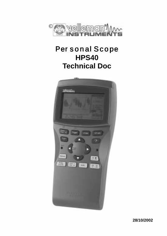
PersonalScopePersonalScopePersonalScopePersonalScope HPS40
Technical Doc
28/10/2002
©
2 © Velleman
HPS40 Technical Doc
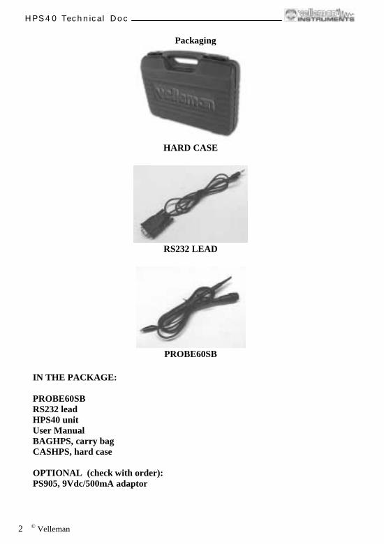
Packaging
HARD CASE
RS232 LEAD
PROBE60SB
IN THE PACKAGE:
PROBE60SBRS232 leadHPS40 unitUser ManualBAGHPS, carry bagCASHPS, hard case
OPTIONAL (check with order):PS905, 9Vdc/500mA adaptor
A division of Velleman Components
SAMPLE FOR APPROVAL
Prepared by: Approved by: Customer acceptance by:Please return signed copy
DATE : DATE : DATE :
None
Includes:HPS40 unitManual and documentsSafety measuring probe (PROBE60S)RS232 connector cablePower supply adaptor SP905 (optional)Carry bag (BagHPS)Hard case (CaseHPS)
Model type :
Description :
Sample number:
Customer :
Remarks / modifications to previous sample:
HPS40
Hand Held Personal Scope
4 © Velleman
HPS40 Technical Doc
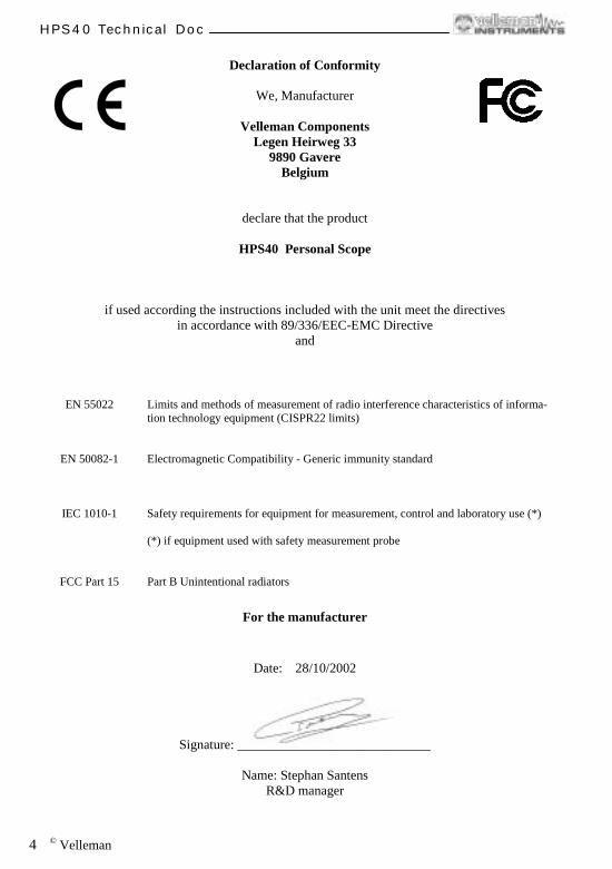
Declaration of Conformity
We, Manufacturer
Velleman ComponentsLegen Heirweg 33
9890 GavereBelgium
declare that the product
HPS40 Personal Scope
if used according the instructions included with the unit meet the directivesin accordance with 89/336/EEC-EMC Directive
and
For the manufacturer
Date: 28/10/2002
Signature: _____________________________
Name: Stephan SantensR&D manager
EN 55022 Limits and methods of measurement of radio interference characteristics of informa-tion technology equipment (CISPR22 limits)
EN 50082-1 Electromagnetic Compatibility - Generic immunity standard
IEC 1010-1 Safety requirements for equipment for measurement, control and laboratory use (*)
(*) if equipment used with safety measurement probe
FCC Part 15 Part B Unintentional radiators
© Velleman 5
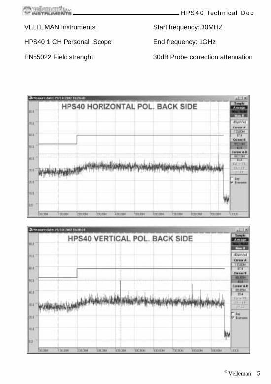
HPS40 Technical Doc
VELLEMAN Instruments
HPS40 1 CH Personal Scope
EN55022 Field strenght
Start frequency: 30MHZ
End frequency: 1GHz
30dB Probe correction attenuation
6 © Velleman
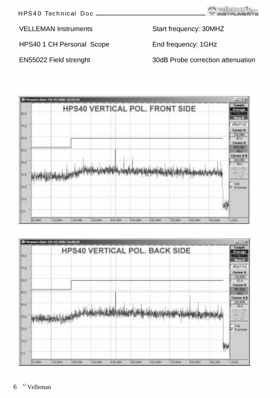
HPS40 Technical Doc
VELLEMAN Instruments
HPS40 1 CH Personal Scope
EN55022 Field strenght
Start frequency: 30MHZ
End frequency: 1GHz
30dB Probe correction attenuation
© Velleman 7
HPS40 Technical Doc
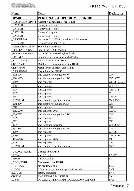
Name Descr DesignatorHPS40 PERSONAL SCOPE BOM 19-06-2002_ASSEMBLY_HPS40 Assembly components for HPS40_BATCLIP+ Battery clip + pole_BATCLIP+- Battery clip + - pole_BATCLIP- Battery clip - pole_BATCLIP-+ Battery clip - + pole_CASEHPS40 Enclosure for HPS40 + window + foil + screws_KBHPS40 Grey keyboard for HPS40_PANHEADSCREW Screw for PCB fixation_SCREENHPS40BK Screen foil HPS40 back side_SCREENHPS40KB screenfoil for HPS40 keyboard side_SERIALNR production serial nr (YY-MM- 00000)_STICK HPS40 Back side info sticker HPS40CKSHPS40C Metal screen on component side HPS40CKSHPS40S Metal screen on solder side HPS40_CAP_HPS40 Capacitors for HPS40_10µ/50V smd electrolytic capacitor 50V C44_100µ/16V smd electrolytic capacitor 16V C47...C57_100N smd capacitor C15...C33, C72
_100P smd capacitor C58, C71_10N smd capacitor C13, C14_15P smd capacitor C6_1N smd capacitor C73...C77_20P/TRIM smd ceramic capacitor trimmer CV1, CV3_22µ/35V smd electrolytic capacitor 35V C45_2N2 smd capacitor C12_2N2/200V smd capacitor 200V C2, C3_33µ/25V smd electrolytic capacitor 25V C46_33P smd capacitor C8, C9_39P smd capacitor C11_4µ7 smd tantalum capacitor C38...C42_4µ7/25V smd electrolytic capacitor 25V C43_470N smd capacitor C34...C37_470P smd capacitor C59...C70_47N/200V smd capacitor 200V C1_47P smd capacitor C10_50P/TRIM smd ceramic capacitor trimmer CV2
_CHOKE_HPS40 Chokes for HPS40_0.68µH smd RF choke L2...L7_150µH smd RF choke L1_CON_HPS40 Connectors for HPS40_HDR1X20 pin header 20-pole LCD1_ST-222 3.5mm stereo jack female pcb with switch SK3BATCON battery connector SK4CBNC05 BNC FEMALE BULKHEAD SK1DJ-005 DC JACK 2.1mm / 5.5mm SOLDER CONNECTIONS SK2
8 © Velleman
HPS40 Technical Doc
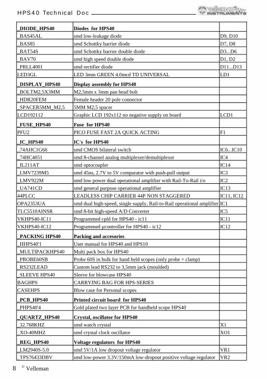
_DIODE_HPS40 Diodes for HPS40
_BAS45AL smd low-leakage diode D9, D10
_BAS85 smd Schottky barrier diode D7, D8
_BAT54S smd Schottky barrier double diode D3...D6
_BAV70 smd high speed double diode D1, D2
_PRLL4001 smd rectifier diode D11...D13
LED3GL LED 3mm GREEN 4.0mcd TD UNIVERSAL LD1
_DISPLAY_HPS40 Display assembly for HPS40
_BOLTM2,5X3MM M2,5mm x 3mm pan head bolt
_HDR20FEM Female header 20 pole connector
_SPACER5MM_M2,5 5MM M2,5 spacer
LCD192112 Graphic LCD 192x112 no negative supply on board LCD1
_FUSE_HPS40 Fuse for HPS40
PFU2 PICO FUSE FAST 2A QUICK ACTING F1
_IC_HPS40 IC's for HPS40
_74AHC1G66 smd CMOS bilateral switch IC6...IC10
_74HC4051 smd 8-channel analog multiplexer/demultiplexer IC4
_IL211AT smd optocoupler IC14
_LMV7239M5 smd 45ns, 2.7V to 5V comparator with push-pull output IC3
_LMV922M smd low power dual operational amplifier with Rail-To-Rail i/o IC2
_UA741CD smd general purpose operational amplifier IC13
44PLCC LEADLESS CHIP CARRIER 44P NON STAGGERED IC11, IC12
OPA2353UA smd dual high-speed, single supply, Rail-to-Rail operational amplifier IC1
TLC5510AINSR smd 8-bit high-speed A/D Converter IC5
VKHPS40-IC11 Programmed cpld for HPS40 - ic11 IC11
VKHPS40-IC12 Programmed µcontroller for HPS40 - ic12 IC12
_PACKING HPS40 Packing and accesories
_HHPS40'1 User manual for HPS40 and HPS10
_MULTIPACKHPS40 Multi pack box for HPS40
_PROBE60SB Probe 60S in bulk for hand held scopes (only probe + clamp)
_RS232LEAD Custom lead RS232 to 3,5mm jack (moulded)
_SLEEVE HPS40 Sleeve for blowcase HPS40
BAGHPS CARRYING BAG FOR HPS-SERIES
CASEHPS Blow case for Personal scopes
_PCB_HPS40 Printed circuit board for HPS40
_PHPS40'4 Gold plated two layer PCB for handheld scope HPS40
_QUARTZ_HPS40 Crystal, oscillator for HPS40
_32.768KHZ smd watch crystal X1
_XO-40MHZ smd crystal clock oscillator XO1
_REG_HPS40 Voltage regulators for HPS40
_LM2940S-5.0 smd 5V/1A low dropout voltage regulator VR1
_TPS76433DBV smd low-power 3.3V/150mA low-dropout positive voltage regulator VR2
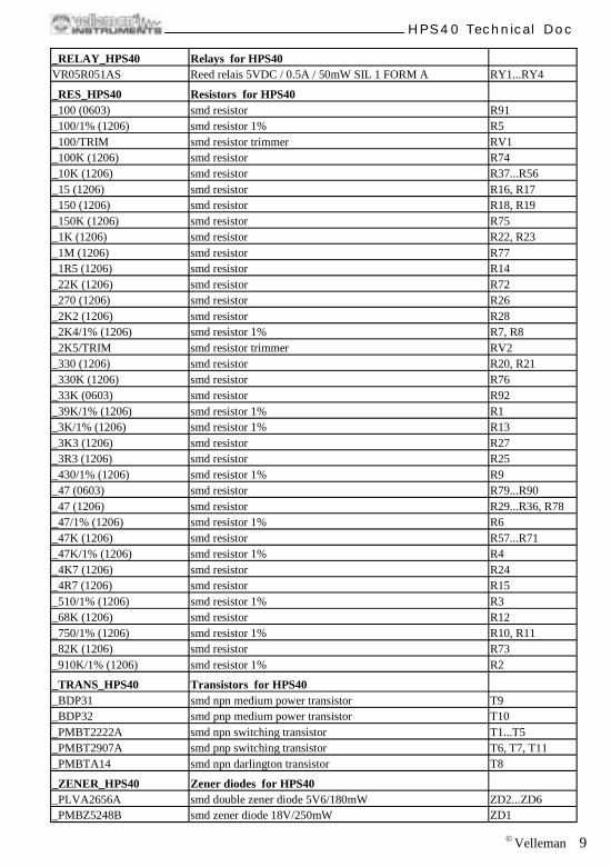
© Velleman 9
HPS40 Technical Doc
_RELAY_HPS40 Relays for HPS40VR05R051AS Reed relais 5VDC / 0.5A / 50mW SIL 1 FORM A RY1...RY4
_RES_HPS40 Resistors for HPS40_100 (0603) smd resistor R91_100/1% (1206) smd resistor 1% R5_100/TRIM smd resistor trimmer RV1_100K (1206) smd resistor R74_10K (1206) smd resistor R37...R56_15 (1206) smd resistor R16, R17_150 (1206) smd resistor R18, R19_150K (1206) smd resistor R75_1K (1206) smd resistor R22, R23_1M (1206) smd resistor R77_1R5 (1206) smd resistor R14_22K (1206) smd resistor R72_270 (1206) smd resistor R26_2K2 (1206) smd resistor R28_2K4/1% (1206) smd resistor 1% R7, R8_2K5/TRIM smd resistor trimmer RV2_330 (1206) smd resistor R20, R21_330K (1206) smd resistor R76_33K (0603) smd resistor R92_39K/1% (1206) smd resistor 1% R1_3K/1% (1206) smd resistor 1% R13_3K3 (1206) smd resistor R27_3R3 (1206) smd resistor R25_430/1% (1206) smd resistor 1% R9_47 (0603) smd resistor R79...R90_47 (1206) smd resistor R29...R36, R78_47/1% (1206) smd resistor 1% R6_47K (1206) smd resistor R57...R71_47K/1% (1206) smd resistor 1% R4_4K7 (1206) smd resistor R24_4R7 (1206) smd resistor R15_510/1% (1206) smd resistor 1% R3_68K (1206) smd resistor R12_750/1% (1206) smd resistor 1% R10, R11_82K (1206) smd resistor R73_910K/1% (1206) smd resistor 1% R2
_TRANS_HPS40 Transistors for HPS40_BDP31 smd npn medium power transistor T9_BDP32 smd pnp medium power transistor T10_PMBT2222A smd npn switching transistor T1...T5_PMBT2907A smd pnp switching transistor T6, T7, T11_PMBTA14 smd npn darlington transistor T8
_ZENER_HPS40 Zener diodes for HPS40_PLVA2656A smd double zener diode 5V6/180mW ZD2...ZD6_PMBZ5248B smd zener diode 18V/250mW ZD1
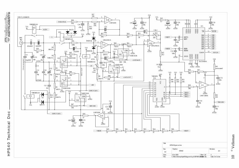
10©
Vel
lem
an
HPS
40
Technic
al D
oc
Title
Number RevisionSize
A4
Date: 3-Oct-2002 Sheet ofFile: C:\Files\Ontwerp\hps40\diagram& pcb\HPS40ed4.ddbDrawn By:
C1
47n/200V
C2
2n2/200V
R19
150
RY1
VR05R051AS
RY2
VR05R051AS
R139K/1%
R2910K/1%
R3510/1%
R447K/1%
R5100/1%
R72K4/1%
R141E5
CV2
50p
CV1
20p
J1
R74
100K
C3
2n2/200V
12
4V
CC
5
GN
D3
IC6 74AHC1G66
12
4
VC
C5
GN
D3
IC7
74AHC1G66
AGND
AGND
5VA
5VA
AC/DC
÷20
÷400
÷1
D9BAS45AL
D10
BAS45AL
5VA
AGND
12
4
VCC5
GND 3IC8 74AHC1G66
AGND
5VA
REFGND
R9
430/1%
R647/1%
R1268K
R8
2K4/1%
12
4
VCC5
GND 3IC9 74AHC1G66
5VAAGND
x1.415/x7.07
R10
750/1%
R11
750/1%
12
4
VCC5
GND 3IC10
74AHC1G66AGND
5VA
x3.325/x6.65
5VA
AGND
R13
3K
RV2
2K5
CAL1OE 1
DB0 3
DB1 4
DB2 5
DB3 6
DB4 7
DB5 8
DB6 9
DB7 10
VD
DD
11
CLKIN 12
VD
DD
13
VD
DA
14
VD
DA
15
REFTS16
REFT17
VD
DA
18
ANIN19
AG
ND
20
AG
ND
21
REFB23
REFBS22
DG
ND
24D
GN
D2
IC5
TLC5510INS
AGND DGND
AGND
AGND
DGNDAGNDAGND
5VA 5VDR15
4.7
C42 4µ7
DB0DB1DB2DB3DB4DB5DB6DB7
ADCLK
ADOE
VREFT
VREFB
R38
10K
R77
1M
R41notmounted
5VD
3
41
52
IC3
LMV7239M5
5VD
TRIGGER
3
2
84
1IC2A
LMV922MR78
47
C38
4µ7
5VA
AGNDAGNDAGND
R29
47
R30
47
R31
47
R32
47
R33
47
R34
47
R35
47
R36
47VREFB VREFT
Y013
Y114
Y215
Y312
Y41
Y55
Y62
Y74
Z 3
VC
C16
VE
E7
GN
D8
S0 11
S1 10
S2 9
E 6
IC474HC4051
DGND
DGNDAGND
5VD
TRIG2TRIG1TRIG0
C41
4µ7
AGNDAGND
5
67IC2B
LMV922M
R58
47K R5947K
R57
47K
RV1100
CAL2
C34
470n
AGND
PWMYPOS
C35
470n
AGND
R39
10K
AGND
R3710K
5VA
D1
BAV70
R48
10K
R47
10K
R46
10K
R45
10K
R4910K
R5010K
R5110K
5VD 5VD 5VD
R253E3
AGND
R44 10K
RY4
VR05R051AS
5VA
D2
BAV70
INPUT CAP2
RY3
VR05R051AS
5VA
INPUT CAP1
CV320p
SK1BNC
5VA
AT
T_CO
M
ATT20
ATT400
INPUT_COMMON
GAIN1
AMP1OUT
GAIN2
R24
4K7
AGND
C58100p
C5
0p
C615p
C7
0p
C10
47p
C11
39p
C12
2n2
C15100n
C27100n
C28100n
C29100n
C30100n
C31100n
C32100n
C33100n
3
21IC1A
OPA2353UA 5
6
84
7IC1B
OPA2353UA
HPS40 Input section
HPS40 4.0
2 4Eddy DeCocker
C72100n
AGND
DGND
C71100p
R91100
C4
15p/200V
C4
notm
ount
ed
©V
elle
man
11
HPS
40
Technic
al D
oc
Title
Number RevisionSize
A4
Date: 3-Oct-2002 Sheet ofFile: C:\Files\Ontwerp\hps40\diagram& pcb\HPS40ed4.ddbDrawn By:
RA0/AN03
RA1/AN14
RA2/AN2/VREF-5
RA3/AN3/VREF+6
RA4/T0CKI7
RA5/SS/LVDIN8
RB0/INT036
RB441
RB2/INT238
RB3/CCP239
RB1/INT137
RB542
RB643
RB744
RC0/T1OSO/T1CKI 16
RC1/T1OSI/CCP2 18
RC2/CCP1 19
RC3/SCK/SCL 20
RC4/SDI/SDA 25
RC5/SDO 26
RC6/TX/CK 27
RC7/RX/DT 29
RD0/PSP0 21
RD1/PSP1 22
RD2/PSP2 23
RD3/PSP3 24
RD4/PSP4 30
RD5/PSP5 31
RD6/PSP6 32
RD7/PSP7 33
RE0/RD/AN5 9
RE1/WR/AN6 10
RE2/CS/AN7 11
VS
S13
VS
S34
MCLR/VPP2 OSC1/CLKIN14 OSC2/CLKOUT/RA6 15
NC1
NC17
NC28
NC40
VD
D12
VD
D35
IC12
PIC18C452/L(44)
DB07
DB18
DB29
DB310
DB411
DB512
DB613
DB714
E6 R/W5 RS4 CS15 RES16
VS
S1
VD
D2
VE
E17
CO
NTR
AS
T3
A 19
K 20
LCD1
LCD-PS192112
PWMCONTRAST
DGND
X1
32.768KHz
DGND DGND
DGND
TRIG INT
PWMYPOS
SW8Contrast
SW12Hold
SW16Display
SW4Mark
ZD3
PLVA2656A
ZD4
PLVA2656A
DGND
DGND
SW7Up
SW11Left
SW15Input
SW3Trig
SW6Right
SW10Down
SW14Auto
SW2tVdiv
SW5ProbeX1
SW9Meter
SW13On/Off
SW1XYpos
VPP 1VDD 2GND 3DATA 4CLK 5SK5
ICSP CONNECTOR DGND
RB6RB7
RB6
RB7
ZD5PLVA2656A
ZD6PLVA2656A
DGNDDGND
R4010K
D8
BAS85
SW17RESET
DGND
DGND
3
26
741 5
IC13
UA741
R75
150K
R61
47K
R60
47K
R73
82K
R76
330K
C36470n
C37
470n
DGND
DGND
PWMCONTRAST
-17.5V
-17.5V
5VD
R1715
R28
2K2
DGND
T1
PMBT2222A
BACKLIGHT
5VD
DGND
5VD
R6247K
DGND
HPS40
HPS40 Digitalsection
SK3
PHONEJACKSTEREOSW
12
65
7
IC14
IL211AT
R18150
R273K3
5VD
RTS
Rx
Tx
ADCLK
ADOEPWR
RDTRIGTIMEDISABLE SYNC
TRIG LEINPUT LE
BACKLIGHT
R4310K
VC
C4
OUT 3TRI1
GN
D2
XO1
40MHz
DGNDDGND IO 1
IO2
IO3
IO4
IO/GCK15
IO/GCK26
IO/GCK37
IO8
IO9
GN
D10
IO11
IO12
IO13
IO14
TDIN15
TMS16
TCK17
IO18
IO19
IO20
VC
CIN
T21
IO22
GN
D23
IO24
IO 25
IO 26
IO 27
IO 28
IO 29
TDOUT 30
GN
D31
VC
CIO
32
IO 33
IO 34
IO 35
IO 36
IO 37
IO 38
IO/GSR 39
IO/GTS2 40
VC
CIN
T41
IO/GTS1 42
IO 43
IO 44
IC11XC9536XL-10PC44C
DGND
3.3VD
INPUT LETRIG LE
DB7DB6DB5DB4DB3
DB2
DB1DB0
RDTRIGTIMEDISABLE SYNC
DGND DGND DGND
DB1DB2DB3DB4DB5DB6DB7
DB0
RS232 Tx
RS232 Tx
TRIG2TRIG1
TRIG0
REFGND
AC/DC÷1
÷20
÷400
x1.415/x7.07
x3.325/x6.65
OSC
OSC
R26270
VCC 1
GND 2
NC 3
TCK 4
NC 5
TDO 6
TDI 7
NC 8
TMS 9
SK6
JTAG CPLD CONNECTOR
DGND
3.3Vcpld
TMS
TDITDO
TCK
TDOTDITMSTCK
DB0DB1DB2DB3DB4DB5DB6DB7
DB0DB1DB2DB3DB4DB5DB6DB7
SK7
PROBETESTPOINT
INPUT CAP1INPUT CAP2
C57
100µ/16V
DGND
DGND
C47
100µ/16V
DGND
RESET
R5410K
R5510K
R5610K
R5310K
5VD
TRIGGERTRIG INT
R5210K
4.5Vcpu
4.0
C59
470p
C60
470p
C61
470p
C62
470p
C63
470p
C64
470p
C65
470p
C66
470p
C67
470p
C68
470p
AGNDAGNDAGNDAGNDAGNDAGNDAGNDAGNDAGNDAGND
R80 47R81 47R82 47R83 47R84 47R85 47R86 47R87 47R88 47R89 47
R79 47
C69
470p
AGND
C70
470p
AGND
R90 47
C26100n
C1310n
C21100n C22100n
C23100n
C24100n
C25
100n
C933p
C833p
3 4Eddy DeCocker
R9233K
L6
0.68µH L70.68µH
3.3Vcpld
C771n
DGND
4.5Vcpu
4.5Vcpu
* R76 =390Kfor lcd with negatif power supply on board
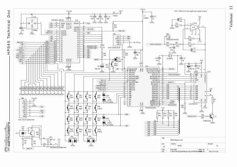
12©
Vel
lem
an
HPS
40
Technic
al D
oc
Title
Number RevisionSize
A4
Date: 3-Oct-2002 Sheet ofFile: C:\Files\Ontwerp\hps40\diagram& pcb\HPS40ed4.ddbDrawn By:
SW
-
+SK2
DCJACK
D11
PRLL4001C48
100µ/16V
IN1 OUT 3
GN
D2
GN
D4
VR1LM2940S-5.0
C49100µ/16V
C50100µ/16V
L1
150µH
5VD
5VA
AGNDDGNDDGNDGNDGNDGNDGND
D12
PRLL4001
GND
+-
SK4BATTERY
D13
PRLL4001
R1615
R20330
LD1
LED3RL
T9
BDP31
GND GND GND
F1FUSE 2A
T10
BDP32
R21330
R67
47K
R65
47K
R6647K
T2PMBT2222A
PWR
GND GND
T4PMBT2222A
T3
PMBT2222A
T6
PMBT2907A
R69
47K
R7147K
R231K
R7047K
R22
1K
R6847K
T5
PMBT2222A
GND GND
GND
GND
PWM
CO
NT
RA
ST
C52
100µ/16V
C53
100µ/16V
C54
100µ/16V
C55
100µ/16V
D3BAT54S
D4BAT54S
D5BAT54S
D6BAT54SGND
C56100µ/16V
GND
C46
33µ/25V
C44
10µ/50V
GND GND GND
R72
22K
ZD1
PMBZ5248B
T7
PMBT2907A
C43
4µ7/25V
DGND DGND
-17.5V
C51
100µ/16V
D7BAS85
T8
PMBTA14
R4210K
ZD2
PLVA2656A
4.5Vcpu
5VD
DGND
DGND
HPS40
HPS40 Powersupply section
IN OUT
GN
DEN BYPASS
VR2
TPS76433DBV
C40
4µ7
DGND DGND DGND DGNDDGND
3.3VD
DGND
C39
4µ7
T11PMBT2907A
4.5Vcpu
R64
47K
R63
47KRESET
4.0
C16100n C17 100n
C18100n
C19
100n
C14
10n
C20100n
4 4Eddy DeCocker
C4522µ/35V
L20.68µH
L30.68µH
C731n
C741n
L40.68µH
L50.68µH
C751n
C761n
* Do notmount thecomponents intothe dashedarea in case ofan lcdwithnegatif power supply on board
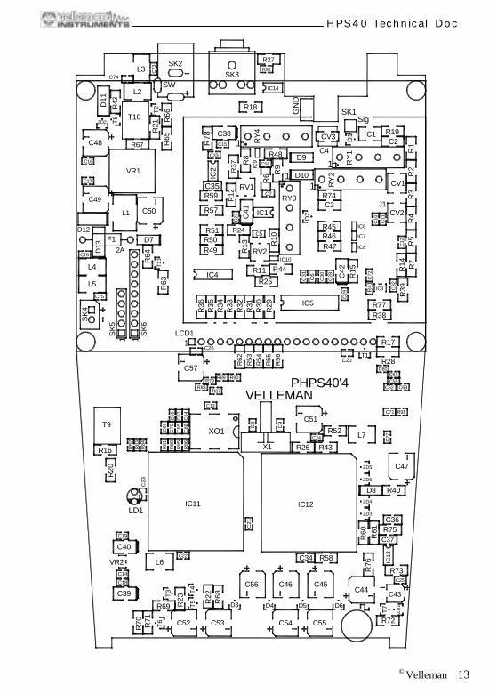
© Velleman 13
HPS40 Technical Doc
VELLEMAN
2A
PHPS40'4R90R89
R88R87
R86
R85
R84
R83
R82
R81
R80
R79
C70
C69
C68
C67
C66
C65
C64
C63C62
C61C60
C59
C1C2
C3
C4
C5
C7
C6
C9
C8
C11
C10
C12
C14
C13
C16
C17
C18
C19
C20
C21
C22
C23
C24
C25
C26
C27
C28
C29
C30
C31
C32
C33
C15
C34
C35
C36
C37
C39
C40
C41
C42
C38
C43C44
C46 C45
C48
C49
C50
C51
C52 C53 C54 C55
C56
CV1
CV3 D1
D2
D3 D4 D5 D6
D7
D8
D9
D10
D11
D12
D13
F1
IC1IC
2
IC3
IC5
IC6
IC7
IC8IC
9IC10
IC13
IC14
J1L1
1LCD1
LD1
R1
R2
R3
R4
R5
R7
R8
R12
R6 R
9R
10R11
R13
R14
R15
R16
R17
R18
R19
R20
R21
R22
R23
R25
R41
R27
R28
R29
R30
R31
R32
R33
R34
R35
R36
R37
R38
R39
R40
R26
R42
R72
R57
R45R46R47
R48
R44
R58
R59
R49R50R51
R66
R65
R67
R68
R69
R70 R71
R43
R60 R61
R62
R73
R74
R75
R76
R77
R78
RV2
1 RY
1
1
RY3
1 RY
4
Sig
GN
D
SK1
SW
SK2
SK3S
K4
1S
K5
1S
K6
T1
T2
T3 T
4T
5
T6
T7
T8
T9
T10
VR1
VR2
X1
XO1
ZD
1
ZD2
ZD3
ZD4
ZD5
ZD6
R24
C47
R64
R52
R53
R54
R55
R56
T11
C58
C71
C72
R91
R92C73
C74
C75
C76
L2
L3
L4
L5
L6
L7
C77
R63
IC11
C57
IC4
RV1 1 RY
2
CV2
IC12
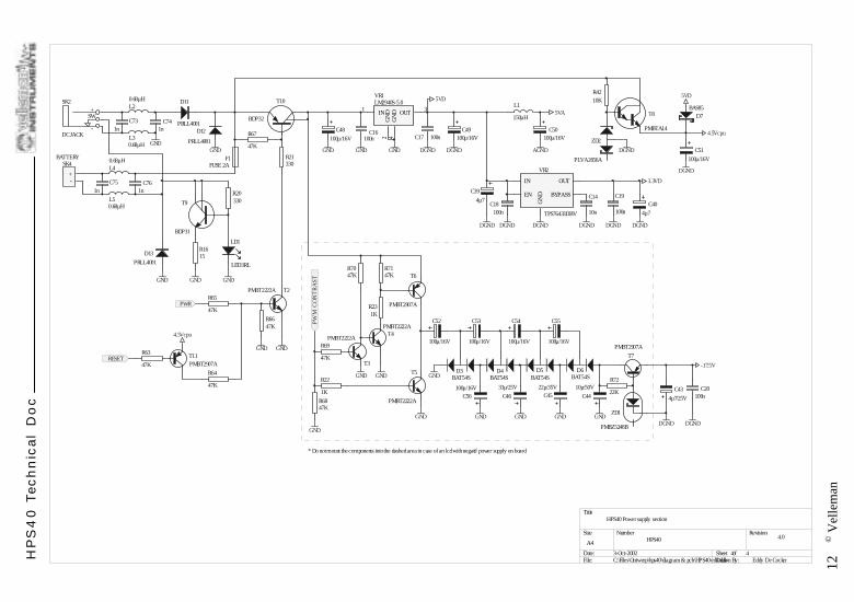
14 © Velleman
HPS40 Technical Doc
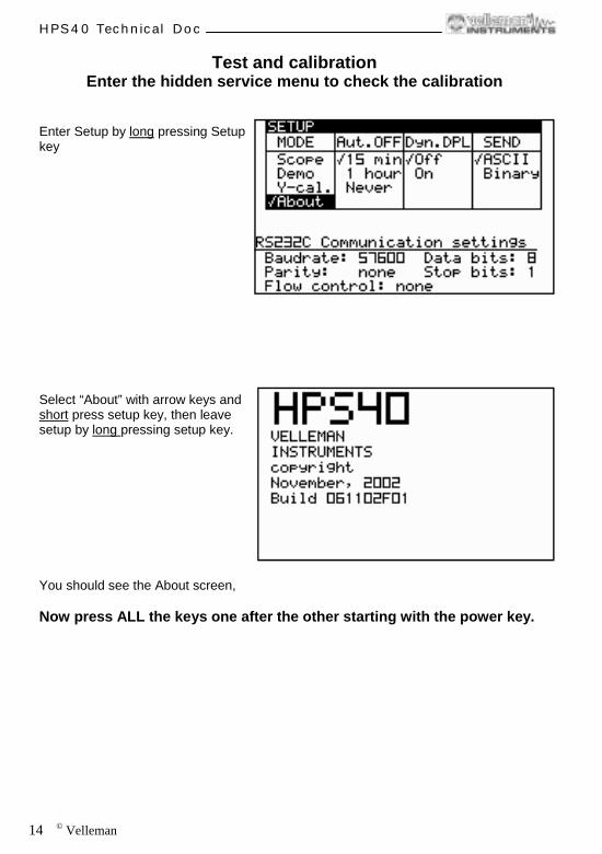
Test and calibrationEnter the hidden service menu to check the calibration
Enter Setup by long pressing Setupkey
Select “About” with arrow keys andshort press setup key, then leavesetup by long pressing setup key.
You should see the About screen,
Now press ALL the keys one after the other starting with the power key.
© Velleman 15
HPS40 Technical Doc
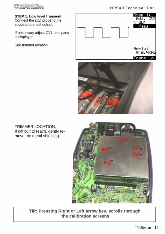
STEP 1, Low level transientConnect the (x1) probe to thescope probe test output,
If necessary adjust CV1 until passis displayed
See trimmer location
TRIMMER LOCATION,If difficult to reach, gently re-move the metal shielding.
TIP: Pressing Right or Left arrow key, scrolls throughthe calibration screens
16 © Velleman
HPS40 Technical Doc
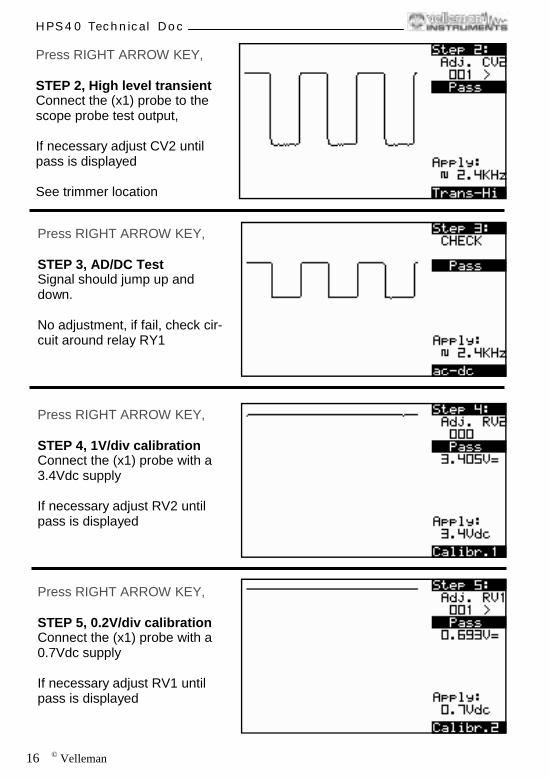
Press RIGHT ARROW KEY,
STEP 2, High level transientConnect the (x1) probe to thescope probe test output,
If necessary adjust CV2 untilpass is displayed
See trimmer location
Press RIGHT ARROW KEY,
STEP 3, AD/DC TestSignal should jump up anddown.
No adjustment, if fail, check cir-cuit around relay RY1
Press RIGHT ARROW KEY,
STEP 4, 1V/div calibrationConnect the (x1) probe with a3.4Vdc supply
If necessary adjust RV2 untilpass is displayed
Press RIGHT ARROW KEY,
STEP 5, 0.2V/div calibrationConnect the (x1) probe with a0.7Vdc supply
If necessary adjust RV1 untilpass is displayed
© Velleman 17
HPS40 Technical Doc
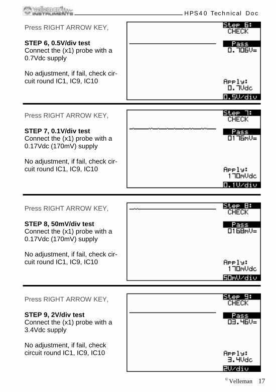
Press RIGHT ARROW KEY,
STEP 6, 0.5V/div testConnect the (x1) probe with a0.7Vdc supply
No adjustment, if fail, check cir-cuit round IC1, IC9, IC10
Press RIGHT ARROW KEY,
STEP 7, 0.1V/div testConnect the (x1) probe with a0.17Vdc (170mV) supply
No adjustment, if fail, check cir-cuit round IC1, IC9, IC10
Press RIGHT ARROW KEY,
STEP 8, 50mV/div testConnect the (x1) probe with a0.17Vdc (170mV) supply
No adjustment, if fail, check cir-cuit round IC1, IC9, IC10
Press RIGHT ARROW KEY,
STEP 9, 2V/div testConnect the (x1) probe with a3.4Vdc supply
No adjustment, if fail, checkcircuit round IC1, IC9, IC10
18 © Velleman
HPS40 Technical Doc
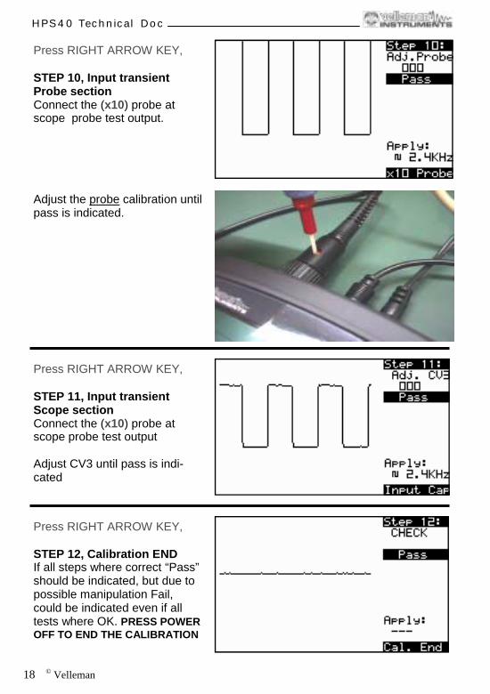
Press RIGHT ARROW KEY,
STEP 10, Input transientProbe sectionConnect the (x10) probe atscope probe test output.
Adjust the probe calibration untilpass is indicated.
Press RIGHT ARROW KEY,
STEP 11, Input transientScope sectionConnect the (x10) probe atscope probe test output
Adjust CV3 until pass is indi-cated
Press RIGHT ARROW KEY,
STEP 12, Calibration ENDIf all steps where correct “Pass”should be indicated, but due topossible manipulation Fail,could be indicated even if alltests where OK. PRESS POWEROFF TO END THE CALIBRATION
©V
elleman
19
HPS
40
Technic
al D
oc
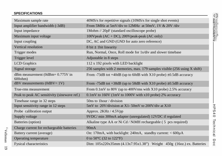
Maximum sample rate 40MS/s for repetitive signals (10MS/s for single shot events)
Input amplifier bandwidth (-3dB) From 5MHz at 5mV/div to 12MHz at 50mV, 1V & 20V /divInput impedance 1Mohm // 20pF (standard oscilloscope probe)
Maximum input voltage 100Vpeak (AC + DC), 200Vpeak-peak (AC only)Input coupling DC, AC and GND (GND for auto zero reference)
Vertical resolution 8 bit ± 1bit linearityTrigger modes Run, Normal, Once, Roll mode for 1s/div and slower timebase
Trigger level Adjustable in 8 steps
LCD Graphics 112 x 192 pixels with LED backlight
Signal storage 256 samples with 2 memories, max. 179 samples visible (256 using X shift)
dBm measurement (0dBm= 0.775V in600ohm)
From -73dB tot +40dB (up to 60dB with X10 probe) ±0.5dB accuracy
dBV measurements (0dBV= 1V) From -75dB tot +38dB (up to 58dB with X10 probe) ±0.5dB accuracy
True-rms measurement From 0.1mV to 80V (up to 400Vrms with X10 probe) 2.5% accuracy
Peak to peak AC sensitivity (sinewave ref.) 0.1mV to 160V (1mV to 1000V with x10 probe) 2% accuracy
Timebase range in 32 steps 50ns to 1hour / divisionInput sensitivity range in 12 steps 5mV to 20V/division at X1- 50mV to 200V/div at X10
Probe calibration output Approx. 2KHz / 4.5Vpp
Supply voltage 9VDC/ min 300mA adapter (unregulated) 12VDC if regulated
Batteries (option) Alkaline type AA or Ni Cd / NiMH rechargeable ( 5 pcs required)
Charge current for rechargeable batteries 90mABattery current (average) On: 170mA, with backlight: 240mA, standby current: < 600µA
Operating temperature 0 to 50°C (32 to 122°F)
Fysical characteristics Dim: 105x220x35mm (4.13x7.95x1.38”) Weight 450g (16oz.) ex. Batteries
SPECIFICATIONS

A division of Velleman® Components Legen Heirweg 33 9890 Gavere BELGIUM Europe www.vellemaninstruments.com HPS40TD1.0


![interoperability.blob.core.windows.netMS-DOC... · Web view[MS-DOC]: Word (.doc) Binary File Format. Intellectual Property Rights Notice for Open Specifications Documentation. Technical](https://static.fdocuments.net/doc/165x107/5cec649388c993031a8d1cca/ms-doc-web-viewms-doc-word-doc-binary-file-format-intellectual-property.jpg)


