Perovskite/Silicon Tandem Solar Cells and Modules
24
Bernd Rech 1 , Daniel Amkreutz 1 , and Steve Albrecht 2 Helmholtz-Center Berlin 1 Institute for Silicon-Photovoltaics 2 Young Investigator Group Perovskite Tandem Solar Cells Perovskite/Silicon Tandem Solar Cells and Modules 2017 EU-US Frontiers of Engineering Symposium, Davis, CA, US, November 16 th, 2017 Many thanks to my colleagues at HZB, cooperation partners and within the FVEE the discussions in the Framework of the ESYS project , University of Ljubljana, colleagues from EPFL and University of Oxford
Transcript of Perovskite/Silicon Tandem Solar Cells and Modules
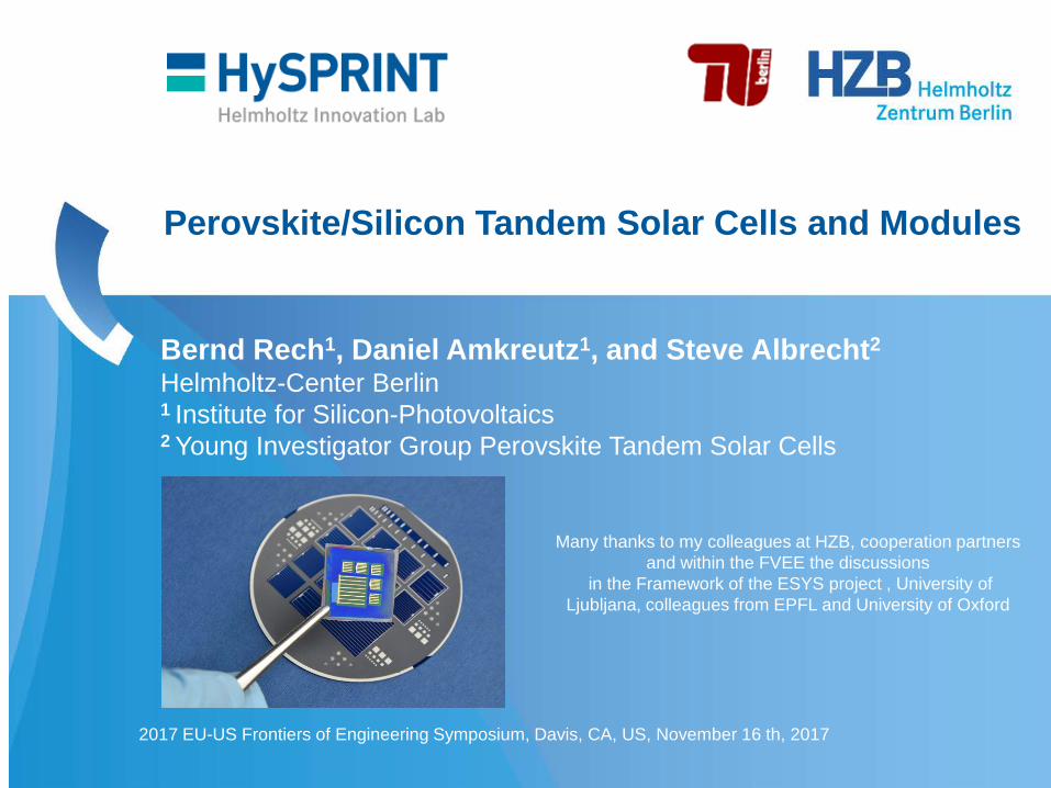
Bernd Rech1, Daniel Amkreutz1, and Steve Albrecht2
Helmholtz-Center Berlin 1 Institute for Silicon-Photovoltaics 2 Young Investigator Group Perovskite Tandem Solar Cells
Perovskite/Silicon Tandem Solar Cells and Modules
2017 EU-US Frontiers of Engineering Symposium, Davis, CA, US, November 16 th, 2017
Many thanks to my colleagues at HZB, cooperation partners
and within the FVEE the discussions in the Framework of the ESYS project , University of
Ljubljana, colleagues from EPFL and University of Oxford
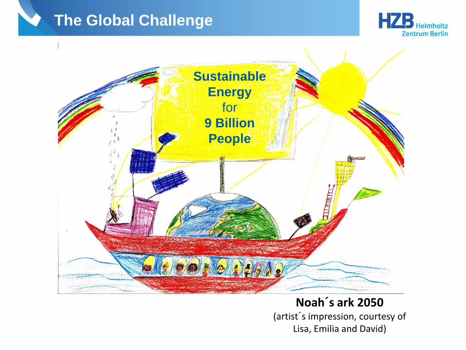
The Global Challenge
Sustainable Energy
for 9 Billion People
Noah´s ark 2050 (artist´s impression, courtesy of
Lisa, Emilia and David)
PV today and tomorrow
from a niche technology to pillar of energy supply Wafer based and thin film crystalline silicon
The working horse of PV c-Si on glass – an example from research High efficiency perovskite solar cells perfect partner for c-Si in tandem solar cells
Conclusion
Outline
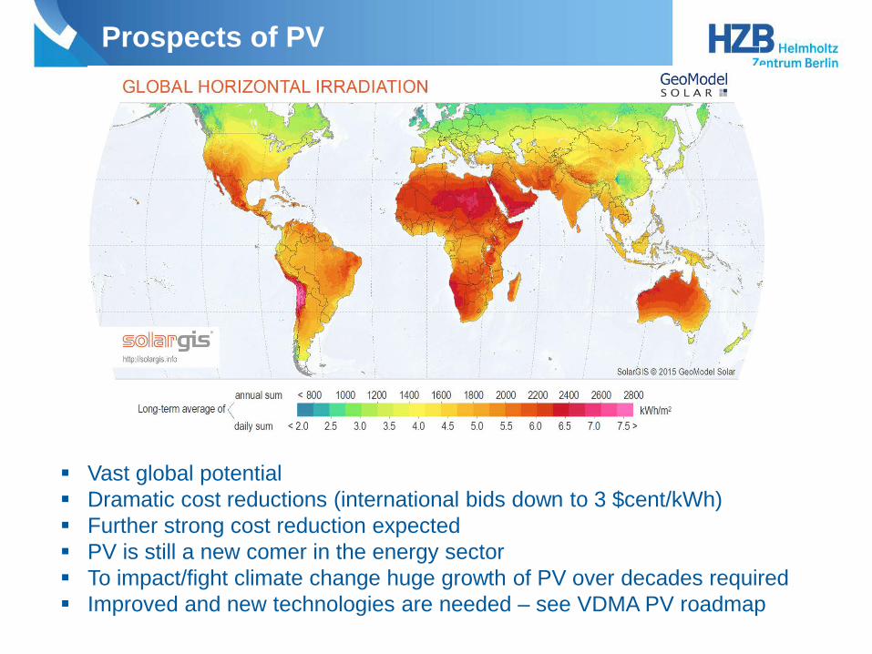
Prospects of PV
Vast global potential Dramatic cost reductions (international bids down to 3 $cent/kWh) Further strong cost reduction expected PV is still a new comer in the energy sector To impact/fight climate change huge growth of PV over decades required Improved and new technologies are needed – see VDMA PV roadmap
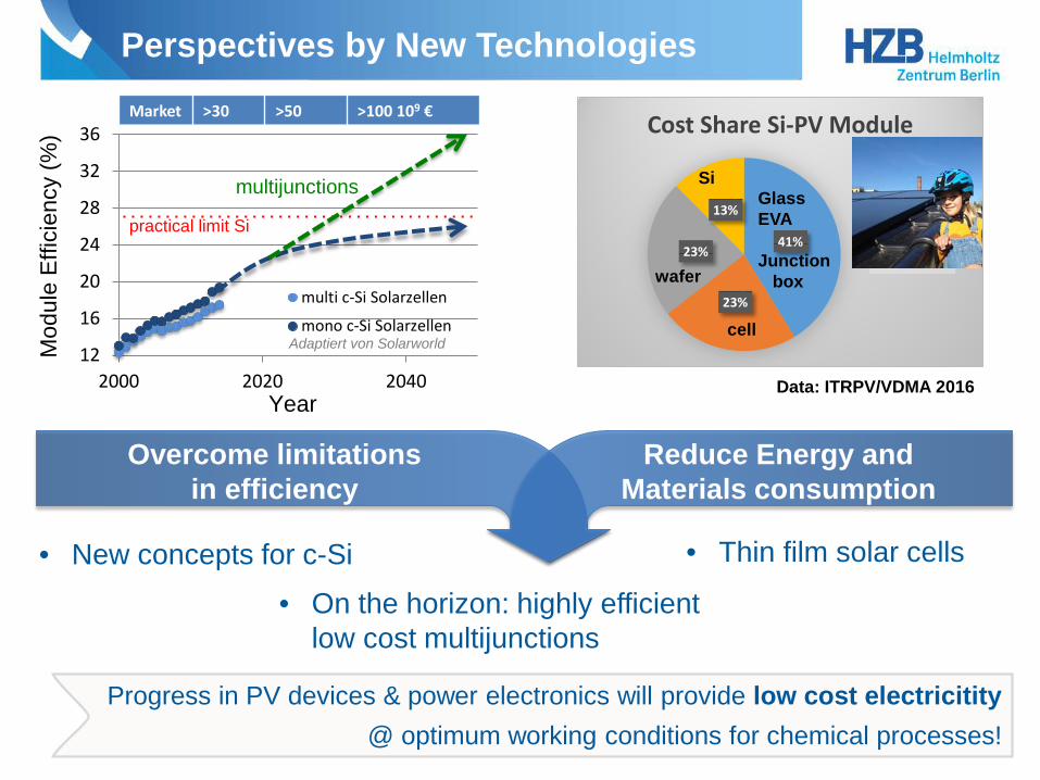
Adaptiert von Solarworld 12
16
20
24
28
32
36
2000 2020 2040
multi c-Si Solarzellen
mono c-Si Solarzellen
Year
Mod
ule
Effi
cien
cy (%
)
practical limit Si
multijunctions
Market >30 >50 >100 109 €
Perspectives by New Technologies
Reduce Energy and Materials consumption
Overcome limitations in efficiency
41%
23%
23%
13%
Cost Share Si-PV Module Module
Zelle
Wafer
Silizium
Si
Data: ITRPV/VDMA 2016
• New concepts for c-Si
• On the horizon: highly efficient low cost multijunctions
• Thin film solar cells
Progress in PV devices & power electronics will provide low cost electricitity @ optimum working conditions for chemical processes!
cell
wafer
Glass EVA Junction box

PV today and tomorrow
from a niche technology to pillar of energy supply
Wafer based and thin film crystalline silicon The working horse of PV
c-Si on glass – an example from research Low cost – high efficiency mulitjunction solar cells
prospects and challenges of perovskite solar cells
Outline
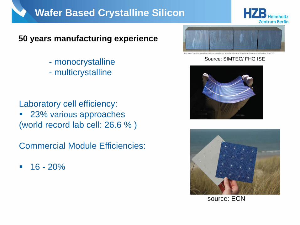
Wafer Based Crystalline Silicon
- monocrystalline - multicrystalline Laboratory cell efficiency: 23% various approaches (world record lab cell: 26.6 % ) Commercial Module Efficiencies: 16 - 20%
50 years manufacturing experience
source: ECN
Source: SIMTEC/ FHG ISE
4 cm² solar cells on 5-inch Cz-Si wafer
Cell area (cm²) values η
(%) VOC
(mV) jSC
(mA/cm²) FF (%)
4 (da) busbars less median 22.3 728 38.3 79.8
best 22.6 730 38.2 81.0
239 (t) 5 busbars best 20.6 722 36.0 79.3
239 cm² solar cell on 6-inch Cz-Si
22.5% (certified)
A. Morales-Viches et al., 33rd EUPVSEC, Amsterdam 2017 (2.AV.3.3) L. Mazzarella et al., 44th IEEE PVSC, Washington 2017, submitted to J-PV
Cell area (cm²)
η (%)
VOC (mV)
jSC (mA/cm²)
FF (%)
1 (da) 23.2 713 41.4 78.5
Stang C., Korte L. et al., Solar RRL 1 (2017) 1700021 Stang C., Korte L. et al., to be published
SiNx
hv
Ag ITO a-Si (i/p/n) c-Si
IBC solar cell with photolithography
Silicon Heterojunction Baseline
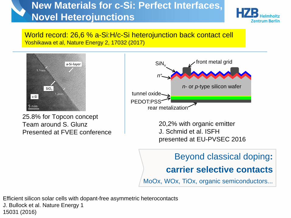
New Materials for c-Si: Perfect Interfaces, Novel Heterojunctions
rear metalization
n+
SiNx
n- or p-type silicon wafer
PEDOT:PSS
front metal grid
tunnel oxide
20,2% with organic emitter J. Schmid et al. ISFH presented at EU-PVSEC 2016
World record: 26,6 % a-Si:H/c-Si heterojunction back contact cell Yoshikawa et al, Nature Energy 2, 17032 (2017)
25.8% for Topcon concept Team around S. Glunz Presented at FVEE conference
Beyond classical doping: carrier selective contacts
MoOx, WOx, TiOx, organic semiconductors...
Efficient silicon solar cells with dopant-free asymmetric heterocontacts J. Bullock et al. Nature Energy 1 15031 (2016)
0
50
100
150
200
250
300
350
400
450
500
coal gas nuclear wind biomass mono-Si multi-Si
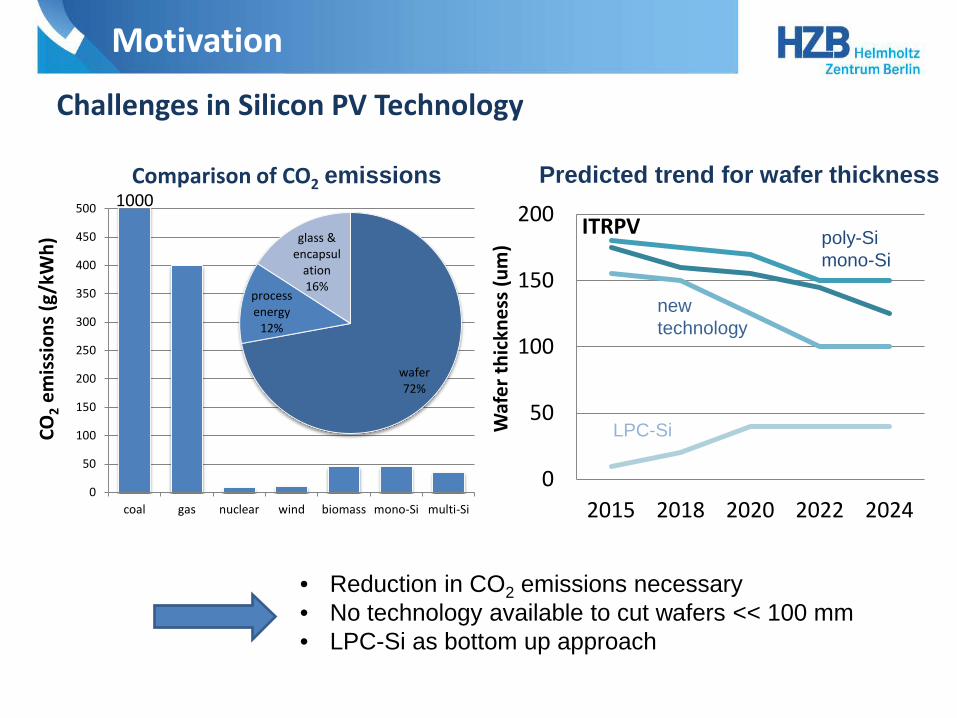
Motivation
Challenges in Silicon PV Technology
CO2 e
mis
sion
s (g/
kWh)
0
50
100
150
200
2015 2018 2020 2022 2024W
afer
thic
knes
s (um
)
LPC-Si
poly-Si mono-Si
new technology
• Reduction in CO2 emissions necessary • No technology available to cut wafers << 100 mm • LPC-Si as bottom up approach
Predicted trend for wafer thickness
wafer 72%
process energy
12%
glass & encapsul
ation 16%
ITRPV
Comparison of CO2 emissions 1000
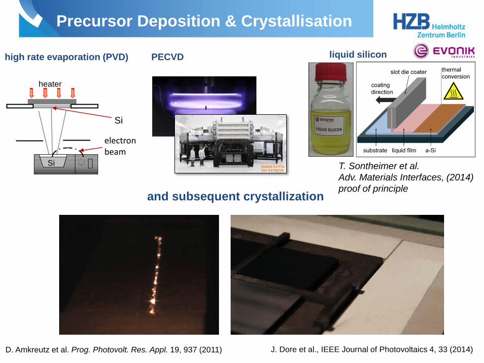
Precursor Deposition & Crystallisation
heater
Si
Si
electron beam
high rate evaporation (PVD) PECVD
D. Amkreutz et al. Prog. Photovolt. Res. Appl. 19, 937 (2011) J. Dore et al., IEEE Journal of Photovoltaics 4, 33 (2014)
and subsequent crystallization
T. Sontheimer et al. Adv. Materials Interfaces, (2014) proof of principle
liquid silicon
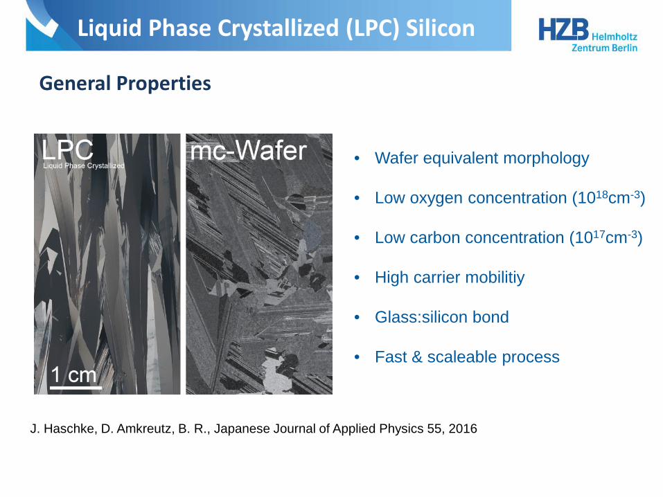
Liquid Phase Crystallized (LPC) Silicon
General Properties
• Wafer equivalent morphology • Low oxygen concentration (1018cm-3) • Low carbon concentration (1017cm-3) • High carrier mobilitiy
• Glass:silicon bond
• Fast & scaleable process
J. Haschke, D. Amkreutz, B. R., Japanese Journal of Applied Physics 55, 2016
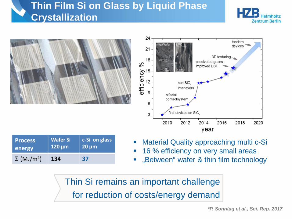
Process energy
Wafer Si 120 µm
c-Si on glass 20 µm
Σ (MJ/m2) 134 37
Material Quality approaching multi c-Si 16 % efficiency on very small areas „Between“ wafer & thin film technology
*P. Sonntag et al., Sci. Rep. 2017
Thin Si remains an important challenge for reduction of costs/energy demand
Thin Film Si on Glass by Liquid Phase Crystallization
PV today and tomorrow
from a niche technology to pillar of energy supply
Wafer based and thin film crystalline silicon The working horse of PV
c-Si on glass – an example from research Low cost – high efficiency mulitjunction solar cells
prospects and challenges of perovskite solar cells
Outline

http://www.med.upenn.edu/chbr/documents/tr_scientific_minds_online_final.pdf
Genomics
Genomics Genomics
Genomics
Health
Perovskite the “Hype Material”
Slide 16
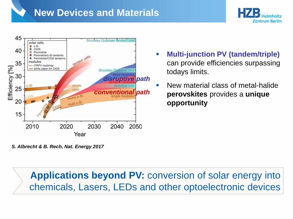
Multi-junction PV (tandem/triple) can provide efficiencies surpassing todays limits.
New material class of metal-halide perovskites provides a unique opportunity
S. Albrecht & B. Rech, Nat. Energy 2017
conventional path
disruptive path
New Devices and Materials
Applications beyond PV: conversion of solar energy into chemicals, Lasers, LEDs and other optoelectronic devices
Si
CdTe
CIGS a-Si
GaAs
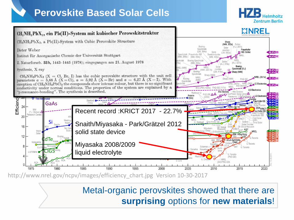
http://www.nrel.gov/ncpv/images/efficiency_chart.jpg Version 10-30-2017
Recent record :KRICT 2017 - 22.7%
Snaith/Miyasaka - Park/Grätzel 2012 solid state device
Miyasaka 2008/2009 liquid electrolyte
Metal-organic perovskites showed that there are surprising options for new materials!
Perovskite Based Solar Cells
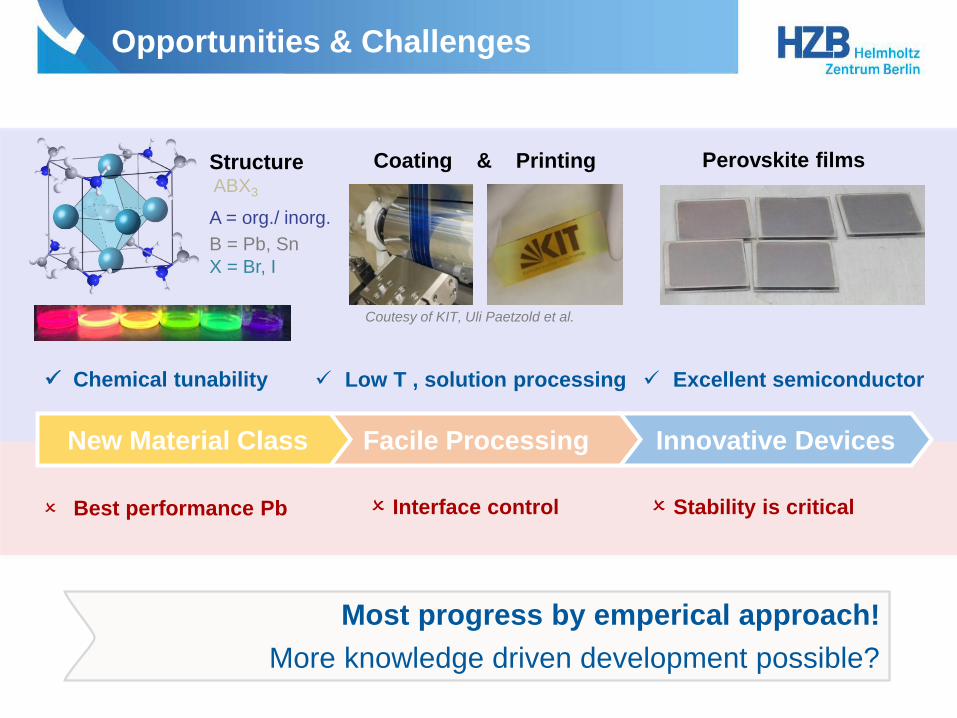
Excellent semiconductor
Perovskite films Coating & Printing
Coutesy of KIT, Uli Paetzold et al.
Low T , solution processing Chemical tunability
Best performance Pb Interface control Stability is critical
A = org./ inorg. B = Pb, Sn X = Br, I
Structure ABX3
Innovative Devices Facile Processing New Material Class
Most progress by emperical approach! More knowledge driven development possible?
Opportunities & Challenges
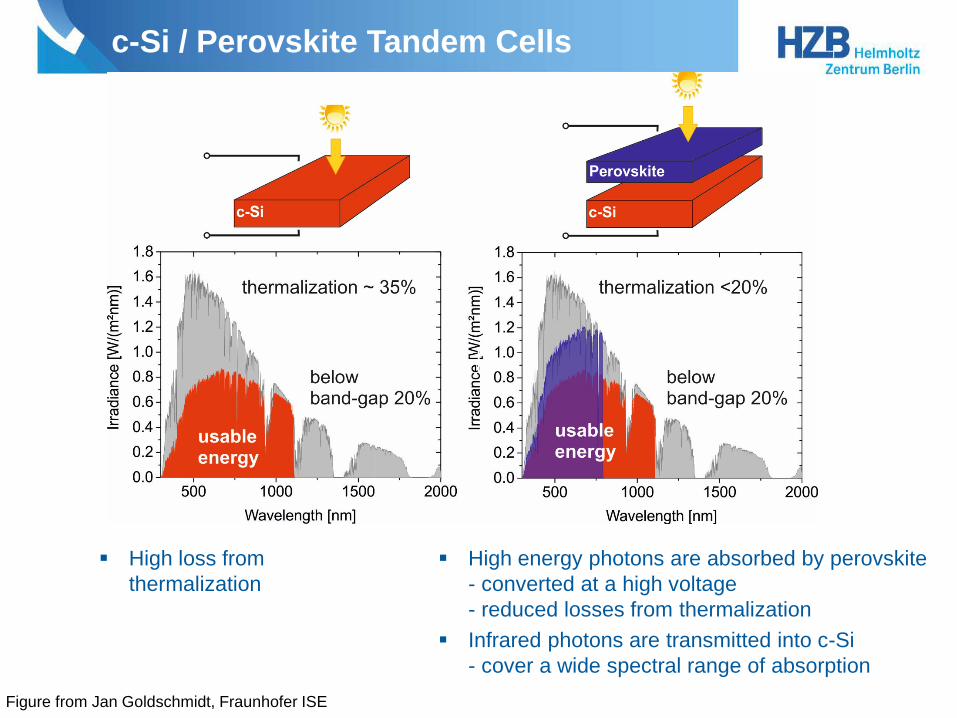
High energy photons are absorbed by perovskite - converted at a high voltage - reduced losses from thermalization
Infrared photons are transmitted into c-Si - cover a wide spectral range of absorption
High loss from thermalization
Figure from Jan Goldschmidt, Fraunhofer ISE
|
c-Si / Perovskite Tandem Cells
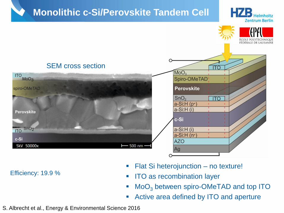
Flat Si heterojunction – no texture! ITO as recombination layer MoO3 between spiro-OMeTAD and top ITO Active area defined by ITO and aperture
SEM cross section
Efficiency: 19.9 %
S. Albrecht et al., Energy & Environmental Science 2016
Monolithic c-Si/Perovskite Tandem Cell
Abs
orpt
ion
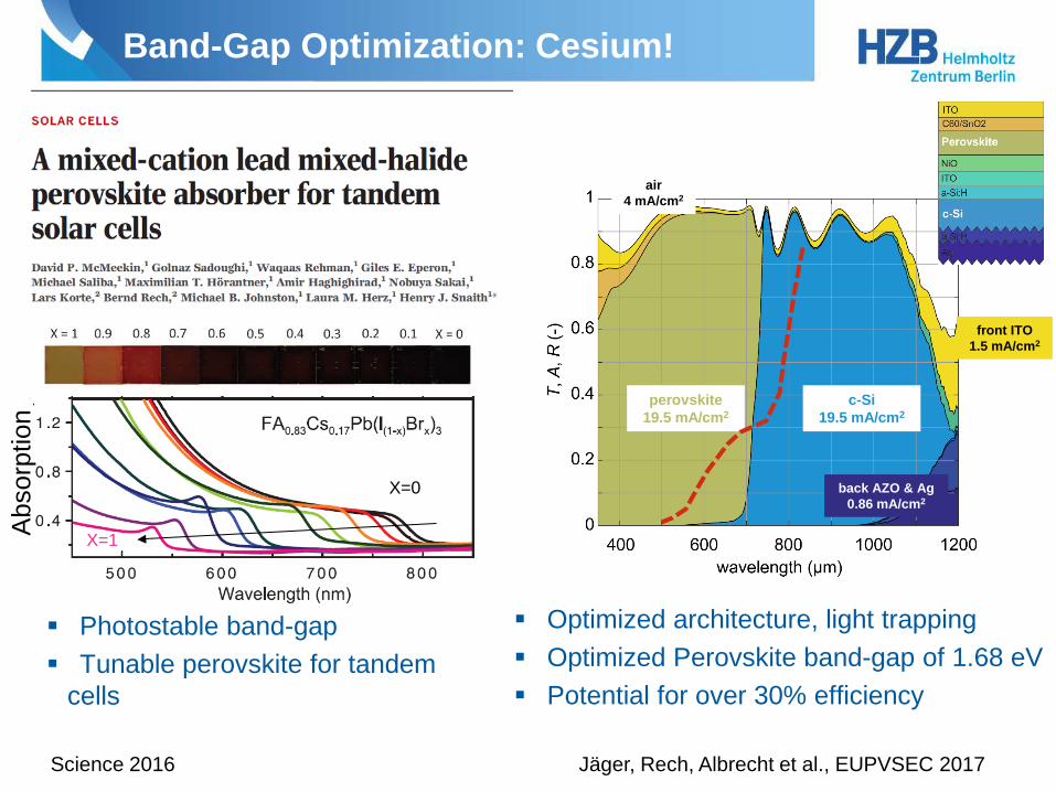
Photostable band-gap Tunable perovskite for tandem
cells
X=0
X=1
Science 2016 Jäger, Rech, Albrecht et al., EUPVSEC 2017
perovskite 19.5 mA/cm2
c-Si 19.5 mA/cm2
air 4 mA/cm2
front ITO 1.5 mA/cm2
back AZO & Ag 0.86 mA/cm2
Optimized architecture, light trapping Optimized Perovskite band-gap of 1.68 eV Potential for over 30% efficiency
Band-Gap Optimization: Cesium!
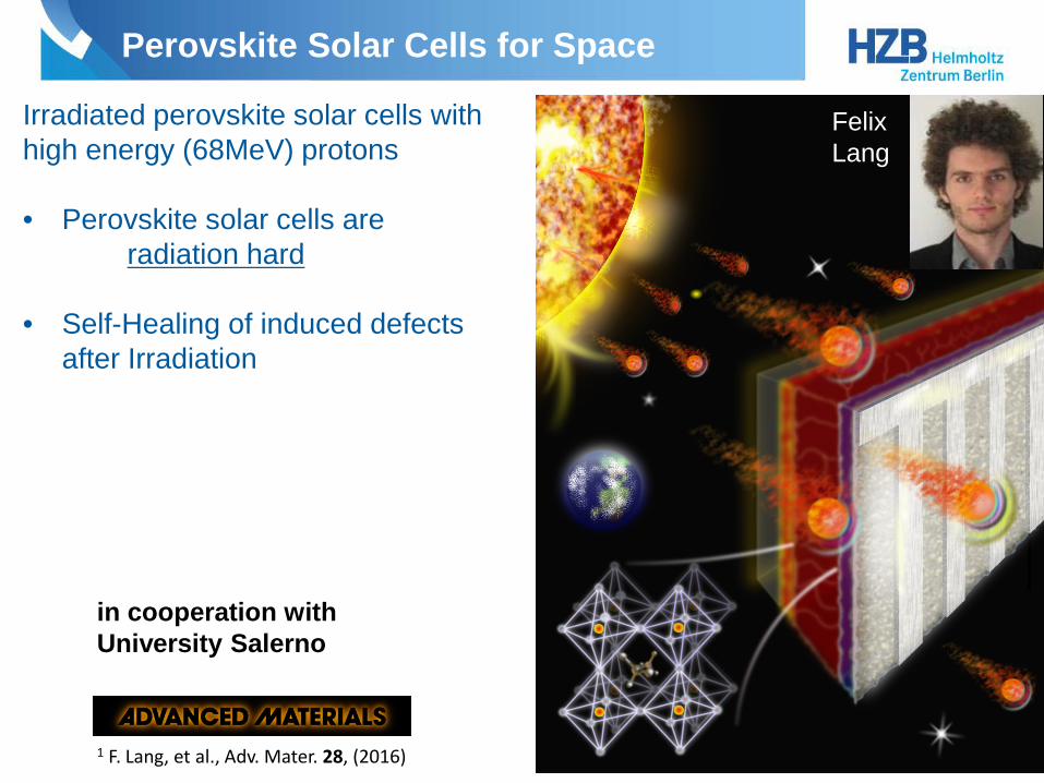
Irradiated perovskite solar cells with high energy (68MeV) protons • Perovskite solar cells are
radiation hard • Self-Healing of induced defects
after Irradiation
1 F. Lang, et al., Adv. Mater. 28, (2016)
in cooperation with University Salerno
Felix Lang
Perovskite Solar Cells for Space
Slide 23
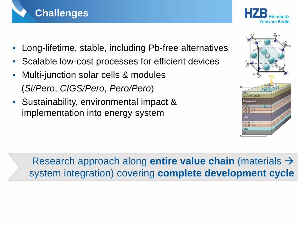
• Long-lifetime, stable, including Pb-free alternatives • Scalable low-cost processes for efficient devices • Multi-junction solar cells & modules (Si/Pero, CIGS/Pero, Pero/Pero) • Sustainability, environmental impact &
implementation into energy system
Research approach along entire value chain (materials system integration) covering complete development cycle
Challenges
Wafer baser crystalline silicon PV dominates the market but is intrinsically limited in efficiency as a single junction technology. • Energy demand for Si wafer production is high – go thin! • Multi-junction-technology
• Efficiency potential of novel hybrid materials has to be transferred into
stable efficiency • Prerequisite: Scalability of processes and equipment
PV has emerged from a niche technology to a global industry
Cheap & efficient & stable & environmentally benign is a must!
The development of new PV technologies relies on breakthroughs in material science, processing and device integration.
Conclusions & Statements


![[Enter your title here] - CreativeCreation - ronn andriessen.pdfTriple cation perovskite for tandem with c-Si cells Absolute efficiency increase of 2.4% compared to standalone c-Si](https://static.fdocuments.net/doc/165x107/60a80cae323c8f08c34d393b/enter-your-title-here-ronn-andriessenpdf-triple-cation-perovskite-for-tandem.jpg)