Perovskite Materials for Light‐Emitting Diodes and Lasers
32
© 2016 WILEY-VCH Verlag GmbH & Co. KGaA, Weinheim 6804 wileyonlinelibrary.com REVIEW Perovskite Materials for Light-Emitting Diodes and Lasers Sjoerd A. Veldhuis, Pablo P. Boix,* Natalia Yantara, Mingjie Li, Tze Chien Sum, Nripan Mathews, and Subodh G. Mhaisalkar* DOI: 10.1002/adma.201600669 1. Introduction The past three years have witnessed an unprecedented advance in the field of solar cells with perovskite metal halide, CH 3 NH 3 PbI 3 , as the primary semiconductor of interest. The archetypical semiconductor forms nearly defect free, crystal- line films that exhibit long-range charge transport and efficient charge collection, yielding solar cells that rival the performance Organic–inorganic hybrid perovskites have cemented their position as an exceptional class of optoelectronic materials thanks to record photovoltaic efficiencies of 22.1%, as well as promising demonstrations of light-emitting diodes, lasers, and light-emitting transistors. Perovskite materials with photo- luminescence quantum yields close to 100% and perovskite light-emitting diodes with external quantum efficiencies of 8% and current efficiencies of 43 cd A −1 have been achieved. Although perovskite light-emitting devices are yet to become industrially relevant, in merely two years these devices have achieved the brightness and efficiencies that organic light-emitting diodes accomplished in two decades. Further advances will rely decisively on the multitude of compositional, structural variants that enable the formation of lower-dimensionality layered and three-dimensional perovskites, nanostruc- tures, charge-transport materials, and device processing with architectural innovations. Here, the rapid advancements in perovskite light-emitting devices and lasers are reviewed. The key challenges in materials development, device fabrication, operational stability are addressed, and an outlook is presented that will address market viability of perovskite light-emitting devices. Dr. S. A. Veldhuis, Dr. P. P. Boix, Dr. N. Yantara, Prof. N. Mathews, Prof. S. G. Mhaisalkar Energy Research Institute at Nanyang Technological University (ERI@N) Research Techno Plaza X-Frontier Block Level 5, 50 Nanyang Drive Singapore 637553, Singapore E-mail: [email protected]; [email protected] Dr. M. Li, Prof. T. C. Sum Division of Physics and Applied Physics School of Physical and Mathematical Sciences Nanyang Technological University 21 Nanyang Link, Singapore 637371, Singapore Prof. N. Mathews, Prof. S. G. Mhaisalkar School of Materials Science and Engineering Nanyang Technological University 50 Nanyang Avenue, Singapore 639798, Singapore of industry-standard silicon, with a veri- fied record efficiency of 22.1%. [1] While much of the research community has been captivated by the potential to chal- lenge silicon photovoltaics, perovskites have nevertheless been making defini- tive strides as promising light-emitting materials with demonstrations of tun- able amplified spontaneous emission and lasers, [2,3] light-emitting diodes (LEDs) in the infrared [4] to bright-green [5] range, phosphor-like applications for yielding white-light emission, and balanced charge injection leading to radiative recombina- tion within the channel of thin-film tran- sistors, [6] yielding red emission. The detailed balance equation requires an external luminescence efficiency of close to 100% to attain the Shockley–Que- isser limit of ≈33.5% for solar cells; thus implying that an excellent solar-cell mate- rial must also be an excellent light emitter. As a result, perovskites have transitioned in a very short time from being a breakthrough material for solar cells to being regarded as an exceptional semiconductor material with wide-ranging applications in light emission. Next-generation light-emitting devices will be distinguished by: i) their high efficiency, high color quality, and tunability, and ii) their low-temperature solution-processing, lowering both the economic and the energetic costs of manufacturing. These challenging objectives will require tuning of the emitter mate- rial, maximizing charge-injection and light-extraction efficien- cies, minimizing non-radiative recombination related losses. Although inorganic LEDs have transformed artificial lighting and brought significant energy savings, these semiconductors rely on high-temperature, expensive vacuum-based processing with epitaxial growth on expensive rigid substrates. The front- runners to replace these III–V semiconductors are organic light- emitting diodes (OLEDs) [7] and colloidal quantum-dot light- emitting diodes (QLEDs). [8] QLEDs are limited by a large non- radiative recombination from the high surface-defect concentra- tion; and although OLEDs have seen commercial applications, these are typically processed via vacuum-based sublimation, a method unsuitable for cost-effective large-area processing. Con- jugated polymers have been pursued for solution processability; however, the critical problem of forbidden (triplet exciton) radiative recombination fundamentally limits their intrinsic emission process. The problems faced by QLEDs and OLEDs would not be seen in perovskites because of the low defect den- sities [2,9,10] and direct bandgap demonstrated. In particular, the Adv. Mater. 2016, 28, 6804–6834 www.advmat.de www.MaterialsViews.com
Transcript of Perovskite Materials for Light‐Emitting Diodes and Lasers

© 2016 WILEY-VCH Verlag GmbH & Co. KGaA, Weinheim6804 wileyonlinelibrary.com
REV
IEW Perovskite Materials for Light-Emitting Diodes and Lasers
Sjoerd A. Veldhuis , Pablo P. Boix , * Natalia Yantara , Mingjie Li , Tze Chien Sum , Nripan Mathews , and Subodh G. Mhaisalkar *
DOI: 10.1002/adma.201600669
1. Introduction
The past three years have witnessed an unprecedented advance in the fi eld of solar cells with perovskite metal halide, CH 3 NH 3 PbI 3 , as the primary semiconductor of interest. The archetypical semiconductor forms nearly defect free, crystal-line fi lms that exhibit long-range charge transport and effi cient charge collection, yielding solar cells that rival the performance
Organic–inorganic hybrid perovskites have cemented their position as an exceptional class of optoelectronic materials thanks to record photovoltaic effi ciencies of 22.1%, as well as promising demonstrations of light-emitting diodes, lasers, and light-emitting transistors. Perovskite materials with photo-luminescence quantum yields close to 100% and perovskite light-emitting diodes with external quantum effi ciencies of 8% and current effi ciencies of 43 cd A −1 have been achieved. Although perovskite light-emitting devices are yet to become industrially relevant, in merely two years these devices have achieved the brightness and effi ciencies that organic light-emitting diodes accomplished in two decades. Further advances will rely decisively on the multitude of compositional, structural variants that enable the formation of lower-dimensionality layered and three-dimensional perovskites, nanostruc-tures, charge-transport materials, and device processing with architectural innovations. Here, the rapid advancements in perovskite light-emitting devices and lasers are reviewed. The key challenges in materials development, device fabrication, operational stability are addressed, and an outlook is presented that will address market viability of perovskite light-emitting devices.
Dr. S. A. Veldhuis, Dr. P. P. Boix, Dr. N. Yantara, Prof. N. Mathews, Prof. S. G. Mhaisalkar Energy Research Institute at Nanyang Technological University (ERI@N) Research Techno Plaza X-Frontier Block Level 5, 50 Nanyang Drive Singapore 637553 , Singapore E-mail: [email protected] ; [email protected] Dr. M. Li, Prof. T. C. Sum Division of Physics and Applied Physics School of Physical and Mathematical Sciences Nanyang Technological University 21 Nanyang Link , Singapore 637371 , Singapore Prof. N. Mathews, Prof. S. G. Mhaisalkar School of Materials Science and Engineering Nanyang Technological University 50 Nanyang Avenue , Singapore 639798 , Singapore
of industry-standard silicon, with a veri-fi ed record effi ciency of 22.1%. [ 1 ] While much of the research community has been captivated by the potential to chal-lenge silicon photovoltaics, perovskites have nevertheless been making defi ni-tive strides as promising light-emitting materials with demonstrations of tun-able amplifi ed spontaneous emission and lasers, [ 2,3 ] light-emitting diodes (LEDs) in the infrared [ 4 ] to bright-green [ 5 ] range, phosphor-like applications for yielding white-light emission, and balanced charge injection leading to radiative recombina-tion within the channel of thin-fi lm tran-sistors, [ 6 ] yielding red emission.
The detailed balance equation requires an external luminescence effi ciency of close to 100% to attain the Shockley–Que-isser limit of ≈33.5% for solar cells; thus implying that an excellent solar-cell mate-rial must also be an excellent light emitter. As a result, perovskites have transitioned
in a very short time from being a breakthrough material for solar cells to being regarded as an exceptional semiconductor material with wide-ranging applications in light emission.
Next-generation light-emitting devices will be distinguished by: i) their high effi ciency, high color quality, and tunability, and ii) their low-temperature solution-processing, lowering both the economic and the energetic costs of manufacturing. These challenging objectives will require tuning of the emitter mate-rial, maximizing charge-injection and light-extraction effi cien-cies, minimizing non-radiative recombination related losses. Although inorganic LEDs have transformed artifi cial lighting and brought signifi cant energy savings, these semiconductors rely on high-temperature, expensive vacuum-based processing with epitaxial growth on expensive rigid substrates. The front-runners to replace these III–V semiconductors are organic light-emitting diodes (OLEDs) [ 7 ] and colloidal quantum-dot light-emitting diodes (QLEDs). [ 8 ] QLEDs are limited by a large non-radiative recombination from the high surface-defect concentra-tion; and although OLEDs have seen commercial applications, these are typically processed via vacuum-based sublimation, a method unsuitable for cost-effective large-area processing. Con-jugated polymers have been pursued for solution processability; however, the critical problem of forbidden (triplet exciton) radiative recombination fundamentally limits their intrinsic emission process. The problems faced by QLEDs and OLEDs would not be seen in perovskites because of the low defect den-sities [ 2,9,10 ] and direct bandgap demonstrated. In particular, the
Adv. Mater. 2016, 28, 6804–6834
www.advmat.dewww.MaterialsViews.com

6805wileyonlinelibrary.com© 2016 WILEY-VCH Verlag GmbH & Co. KGaA, Weinheim
REV
IEW
intrinsic properties of organometallic halide perovskites, such as formation of nearly defect-free, [ 11 ] crystalline fi lms at low temperatures (≈70–100 °C), high optical absorption/emission wavelength tunability, long-range ambipolar transport, effi cient charge transfer, and injection to and from metallic contacts, are essential in its applicability to both solar cells and light-emitting devices. The electrical (e.g., diffusion length, mobility) and optical (e.g., photoluminescence quantum yield) qualities of metal halide perovskites, in the vicinity of the ones observed in inorganic semiconductors such as Si or GaAs, have manifested themselves in effective electroluminescence, optically pumped amplifi ed spontaneous emission (ASE), and lasing. These applications require the generation of high amounts of local-ized charge carriers, so that the high extinction coeffi cient, low exciton binding energy, and large diffusion lengths of solution-processed CH 3 NH 3 PbI 3 were assiduously leveraged.
The key parameter that serves as a fi gure of merit for high-performance light-emitting materials is the photoluminescence quantum yield (PLQY) – defi ned as the ratio of emitted photons to those absorbed. On the LED level, the radiant effi ciency (RE) or wall plug effi ciency (WPE) is the electrical-to-optical energy-conversion effi ciency, [ 12 ] and may be described as:
RE orWPE EQE LE IQE /injection extraction L I Vη η ( )( ) = ⋅ = ⋅ ⋅ ⋅ ⋅ ( 1)
Here, the external quantum effi ciency (EQE) is defi ned as the ratio of emitted photons to the number of electrons injected into the device, η injection is the proportion of electrons injected into the active emitter layer to the number of electrons passing through the device; the internal quantum effi ciency (IQE) [ 13,14 ] is the proportion of electron–hole recombinations that occur radiatively in the emitter layer; η extraction is the proportion of generated photons in the emitter layer that exit the device; and the luminous effi cacy (LE) is the ratio of emitted ( L ) to injected energy ( I V ) by the source.
Amongst this multitude of metrics, the key fi gures of merit may include: i) the EQE, which measures how effi ciently the device converts electrons to photons, ii) the brightness (cd m −2 ), and iii) the current effi ciency (CE) (cd A −1 ). There is a correla-tion between effi cient LED materials and suitable gain and laser materials. The light-emitting material used in an LED can, in principle, also be used as a gain medium in a laser, if it is pos-sible to achieve the transition from spontaneous emission to stimulated emission at higher input carrier densities. Indeed, the ultralow amplifi ed spontaneous emission (ASE) thresholds of organometallic halide perovskites provide a strong impetus for light-emission applications using halide perovskites.
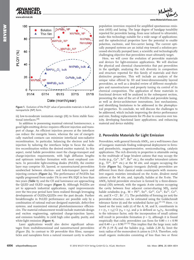
The extraordinary enhancement in the PLQY in the past two years ( Figure 1 ) has now placed perovskites on a par with the best-in-class solution-processed semiconductors, and it is an affi rmation of the applicability of perovskites as light-emitting materials. Different approaches, such as the synthesis of lower-dimensionality layered perovskites to increase the binding energies and oscillator strengths of the excitons, or increasing the spatial confi nement, have been applied to maximize PLQYs (Figure 1 ). The high photoluminescence combined with the compositional fl exibility of these materials place perovskites as robust technological candidates, distinguished by: i) high color purity (FWHM ≈ 20 nm), [ 15 ] irrespective of size of the
Sjoerd A. Veldhuis obtained his Ph.D. in inorganic mate-rials science from MESA+ Institute for Nanotechnology, at the University of Twente (The Netherlands) in 2015. During this period he studied in-depth the formation of inorganic nanomaterials from wet-chemical synthesis routes. He currently works as a research fellow at the
Energy Research Institute at Nanyang Technological University (ERI@N) in Singapore. His current research focuses on fabrication of nanostructured materials for light-emission and energy applications.
Pablo P. Boix received his Ph.D. from the Universitat Jaume I (2012, Castelló, Spain). During this period, he analyzed the physical processes of optoelectrical devices including DSC, QDSC, organic solar cells, and water-splitting systems by impedance spectroscopy. In 2012 he joined the Energy Research Institute at Nanyang
Technological University (ERI@N), where his research focuses on the development of perovskite photovoltaic and light-emitting devices, elucidating the working mecha-nisms that determine their performance.
Subodh G. Mhaisalkar is the Tan Chin Tuan Centennial Professor in the School of Materials Science & Engineering at the Nanyang Technological University (NTU), Singapore. He is also the Executive Director of the Energy Research Institute at NTU (ERI@N), a pan-University multidisciplinary research institute for innova-
tive energy solutions. Prior to joining NTU in 2001, he had over 10 years of research and engineering experience in the microelectronics industry. He received his Bachelors’ degree from IIT-Bombay, India and his MS/Ph.D. degrees from The Ohio State University, USA.
crystallites due to the in-built quantum well structure in low-dimensionality perovskites; [ 16,17 ] ii) bandgap tunability to cover the entire spectrum of visible light and hence for engi-neering white-light emission in layered perovskites; [ 18,19 ] and
Adv. Mater. 2016, 28, 6804–6834
www.advmat.dewww.MaterialsViews.com
6806 wileyonlinelibrary.com © 2016 WILEY-VCH Verlag GmbH & Co. KGaA, Weinheim
REV
IEW
iii) low-to-moderate ionization energy (IE) to form stable func-tional interfaces. [ 20 ]
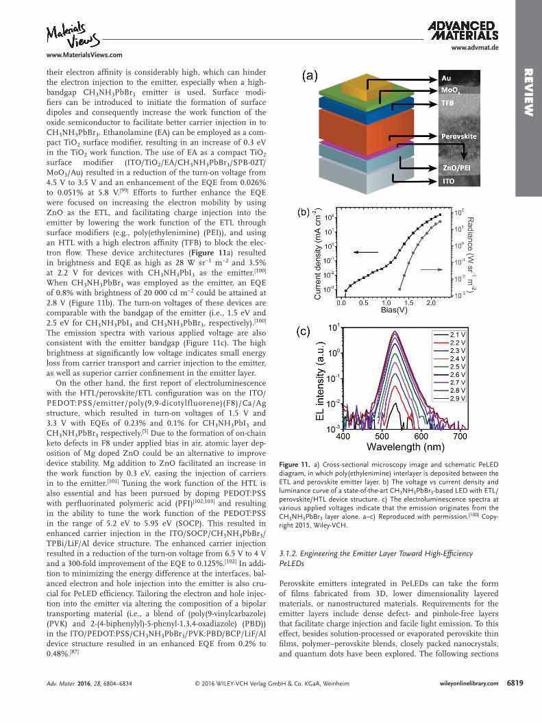
In addition to possessing maximal external luminescence, a good light-emitting device requires effi cient injection and trans-port of charge. An effi cient injection process at the interfaces can reduce the energetic losses, whereas the use of energeti-cally matched contacts can minimize interfacial non-radiative recombination. In particular, balancing the electron and hole injection by tailoring the interfaces helps to focus the radia-tive recombination within the desired emitter material. In this aspect, metal halide perovskites meet the charge-transport and charge-injection requirements, with high diffusion lengths and optimum interface formation with most employed con-tacts. In perovskite light-emitting diodes (PeLED), the emitter layer may comprise 3D, layered, or nanostructured perovskites sandwiched between electron- and hole-transport layers and injecting contacts ( Figure 2 a). The performance of PeLEDs has rapidly progressed from under 1% to over 8% EQE in less than two years ( Table 1 ); and the CE and luminance are approaching the QLED and OLED ranges ( Figure 3 ). Although PeLEDs are yet to approach industrial applications, rapid improvements over the two-year period have been realized through leveraging developments of OLEDs/QLEDs over the past decade. Further breakthroughs in PeLED performance are possible only by a combination of rational end-use designed materials, defect-free systems, and maximized external photoluminescence effi cien-cies. The material enhancement would include materials design and exciton engineering, optimized charge-injection layers, and emission tunability, to yield high color quality, purity, and white-light emission ( Figure 4 ).
Laser applications would also derive signifi cant advan-tages from multidimensional and nanostructured perovskites (Figure 2 b). In contrast to 3D perovskite thin fi lms, nanopar-ticles and nanoplates form a natural resonant cavity to achieve
population inversion required for amplifi ed spontaneous emis-sion (ASE) and lasing. The large degree of bandgap tunability reported for perovskite lasing, from near infrared to ultraviolet, make this technology suitable for a wide range of applications; and the optoelectrical properties have the potential to enable polariton, excitonic, and free-carrier lasing. The current opti-cally pumped systems are an initial step toward a solution-pro-cessed electrically pumped laser, a scientifi c and technologically challenging objective that perovskites must ultimately target.
Here, we will cover the evolution of perovskite materials and devices for light-emission applications. We will disclose the physical and chemical characteristics that put perovskites in the spotlight, analyzing the rich diversity in composition and structure reported for this family of materials and their distinctive properties. This will include an analysis of the unique value offered by 3D and lower-dimensionality layered perovskites, as well as a detailed review of different morpholo-gies and nanostructures and property tuning via control of its chemical composition. The application of these materials in functional devices will be analyzed in the subsequent section, presenting the state of the art of PeLEDs and perovskite lasing, as well as device-architecture innovations, loss mechanisms, and identifying limitations to be addressed in the photophys-ical properties. To conclude, we will discuss the challenges to be addressed, which include improving the device performance and size, fi nding replacements for Pb due to concerns over tox-icity, developing functional laser applications, and enhancing material and device stability.
2. Perovskite Materials for Light Emission
Perovskites, with general formula AMX 3 , are a well-known class of inorganic materials fi nding widespread deployment in ferro- and piezoelectric, magnetoresistive, semiconducting, catalysis applications. The rich diversity in properties is attainable owing to the multitude of large bivalent cations that may occupy the A-site (e.g., Ca 2+ , Sr 2+ , Ba 2+ etc.), the smaller tetravalent cations (e.g., Ti 4+ , Zr 4+ etc.) at the M site, and oxygen occupying the X-site ( Figure 5 a). Organic–inorganic (hybrid) perovskites are different from their classical oxide counterparts with monova-lent organic moieties introduced on the A-site, divalent metal cations at the M site, and, typically, halides at the X-site. The AMX 3 hybrid perovskite structure is formed by a three-dimen-sional (3D) network, with the organic A-site cations occupying the cavity between four adjacent corner-sharing MX 6 metal halide octahedra (e.g., M = Pb 2+ , Sn 2+ , Ge 2+ , Cu 2+ , Eu 2+ , Co 2+ , etc. and X = Cl − , Br − , I − ). The probability of forming (or not) the perovskite structure, can be estimated using the Goldschmidt tolerance factor ( t ) and the octahedral factor ( µ ). [ 21–23 ] Here, t is based on the ionic radii ( r ) of the A, M, and X, constituents in t = ( r A + r X )/√2 ( r M + r X ), and µ is defi ned as r M / r X . According to the tolerance factor, only the incorporation of small cations will result in perovskite formation ( t ≈ 1), although it is found empirically that cubic perovskites can form for 0.80 < t < 0.90 and 0.40 < µ < 0.90. [ 22–25 ] This implies that the large ionic radii of Pb (1.19 Å) and the halides (e.g., iodide 2.20 Å), limit the ionic radius of the monovalent A cation to 2.9 Å. Therefore, only small organic molecules consisting of less than two or three
Adv. Mater. 2016, 28, 6804–6834
www.advmat.dewww.MaterialsViews.com
Figure 1. Evolution of the PLQY value of perovskite materials in bulk and nanoparticle (NP) form.

6807wileyonlinelibrary.com© 2016 WILEY-VCH Verlag GmbH & Co. KGaA, Weinheim
REV
IEW
C–C or C–N bonds, or inorganic cations such as Cs + (1.88 Å), are expected to fi t in the 3D hybrid perovskite structure. [ 24 ]
The fi rst reports on light emission [ 26–28 ] and lasing [ 29 ] from hybrid perovskites were published in the 1990s. For example, large crystals of (C 6 H 5 (CH 2 ) 2 NH 3 ) 2 PbI 4 obtained via simple acid–base reactions, showed intense electroluminescence after applying a voltage of 24 V at liquid-nitrogen tempera-tures. [ 26 ] This layered perovskite material offers the possibility of enhanced structural stability from an inorganic backbone, while the optical properties can be tuned by the organic cation. To overcome the low-temperature limitation, a double-proto-nated 5,5′′′-bis(2-aminoethyl)-2,2′:5′,2′′:5′′,2′′′-quaterthiophene (AEQT) dye was used as an organic constituent in the hybrid structure, demonstrating room-temperature electrolumines-cence. [ 30 ] However, (AEQT) 2 PbBr 4 -based devices could only be fabricated via a thermal-ablation method, since solution-pro-cessing was not possible due to the low solubility of the AEQT dye in common solvents and their incompatible wettability with the substrate. After that, only a few accounts on light emission
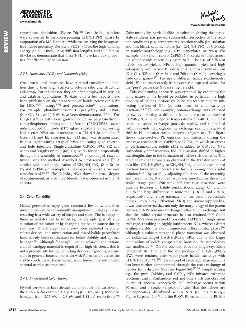
from perovskites were reported, and the fi eld seemed dormant for more than a decade. It was only in 2014 that room-temper-ature light emission from solution-processed CH 3 NH 3 PbX 3 perovskites was demonstrated. [ 2,5 ] Compared to expensive, vacuum-based processing of currently used solid-state light-emitting devices, the low-temperature processing conditions pose a very attractive alternative toward cost-effective large-area optoelectronic applications. Following the breakthrough per-formance of perovskites in photovoltaic devices, CH 3 NH 3 PbI 3 and its anion-substituted analogues were shown to display amplifi ed spontaneous emission at thresholds as low as 12 µJ cm −2 . [ 2,31 ] In addition, it was also demonstrated that typical solar-cell architectures (with a mesoporous TiO 2 scaffold) also exhibit ASE at very low optical pump fl uence thresholds (Figure 5 b). [ 2 ] The fi rst demonstration of LEDs was also based on the halide-substituted CH 3 NH 3 PbX 3 family (Figure 5 c). [ 5 ] By tuning the halide composition of the perovskite, the devices displayed bright-green (517 nm) and red (630 nm) EL emis-sion, with EQEs ranging 0.1–0.4%, respectively. Besides the
Adv. Mater. 2016, 28, 6804–6834
www.advmat.dewww.MaterialsViews.com
Figure 2. Schematic representation of a PeLED device concept (a) and a perovskite laser device concept (b).

6808 wileyonlinelibrary.com © 2016 WILEY-VCH Verlag GmbH & Co. KGaA, Weinheim
REV
IEW
devices based on the CH 3 NH 3 PbX 3 family, LEDs based on inorganic CsPbBr 3 were also recently reported. [ 32 ] In addition to light-emission from thin emitter fi lms, bright emission was also observed from nanostructured (nanoparticles, nanoplates, and nanowires) organic–inorganic and all-inorganic perov-skites. [ 15,33–36 ] The propensity for tuning of the photophysical properties via cationic and anionic substitutions along with the additional range afforded by size and morphology manipula-tion amount to a broad palette of possibilities for light-emitting devices.
2.1. 3D Perovskites and Lower-Dimensionality Layered Perovskites
2.1.1. 3D Perovskites
The effective light-emission from organic–inorganic hybrid perovskites originates from their remarkable properties, such as low defect densities, low non-radiative recombina-tion, and high photoluminescence. The fi rst demonstrated device achieved effective bimolecular recombination by spatial confi nement of electrons and holes within the thin emitter layer (≈15 nm), thus overcoming the low exciton binding energy of the perovskite. [ 5 ] The devices displayed bright-green
(CH 3 NH 3 PbBr 3 ; EL at 517 nm) and red (CH 3 NH 3 PbBr 2 I; EL at 630 nm) EL emission, with EQEs ranging 0.1–0.4%, respectively, with a maximum brightness of 364 cd m −2 for the green-emitting device. Commonly, thin emitter fi lms are prepared via spin-casting methods, in which dissolved pre-cursors are spread on a substrate at high rotational speeds. For improved thin-fi lm morphology, one-step and sequential-deposition techniques (adopted from photovoltaic devices) are often employed. [ 37 ] For optimal light-emission from thin fi lms, high surface coverage and smooth morphology are prerequi-sites, as non-radiative losses originating from shunt paths (e.g., due to incomplete surface coverage or pinholes) result in lower emission. By embedding the perovskite materials in a polymer matrix, pinhole-free fi lms were obtained from polyimide [ 38 ] or poly(ethylene oxide) [ 39 ] matrices and improved luminescence performance were displayed. Additionally, it has been suggested that the formation of metallic Pb (e.g., from incomplete perovs-kite formation at stoichiometric precursor ratios) [ 40 ] may lead to non-radiative decay pathways originating from these defect trap states, thus posing a challenge to high luminescence effi ciency in light-emitting devices. Addition of excess CH 3 NH 3 Br during fi lm deposition has been attributed to the suppression of Pb formation and improved effi ciencies. [ 40 ] It should be noted that this observation is in contrast to the need for excess lead reported for solar-cell applications, [ 41 ] and further investigations
Adv. Mater. 2016, 28, 6804–6834
www.advmat.dewww.MaterialsViews.com
Table 1. Overview of selected representative results of light-emission from organic–inorganic and all-inorganic halide perovskite in LEDs.
Perovskite Emitter a) Morphology Device architecture b,c) EQE [%]
CE [cd A −1 ]
L max [cd m −2 ]
V T [V]
Publication date (month-year)
CH 3 NH 3 PbBr 3 [ 5 ] Thin fi lm ITO/PEDOT:PSS/Pe/F8/Ca/Ag 0.1 0.3 364 3.3 08-2014
CH 3 NH 3 PbBr 3 [ 102 ] Thin fi lm ITO/Buf-HIL/Pe/TPBI/LiF/Al 0.125 0.57 417 ≈4 11-2014
CH 3 NH 3 PbBr 3 [ 149 ] Thin fi lm ITO/PEDOT:PSS/TPD/Pe/Ag 6.5 × 10 −3 ≈1.8 × 10 −2 21 ≈4 01-2015
CH 3 NH 3 PbI 3− x Br x [ 149 ] (red) Thin fi lm ITO/PEDOT:PSS/TPD/Pe/Ag 1.1 × 10 −3 n.r. d) n.r. n.r. 01-2015
CH 3 NH 3 PbBr 3 [ 101 ] Thin fi lm ITO/PEDOT:PSS/Pe/ZnO/Ca/Ag n.r. ≈21 ≈550 2 01-2015
CH 3 NH 3 PbBr 3 [ 38 ] Thin fi lm ITO/PEDOT:PSS/Pe-PIP/F8/Ca/Ag 1.2 n.r. ≈200 n.r. 02-2015
CH 3 NH 3 PbBr 3 [ 100 ] Thin fi lm ITO/ZnO-PEI/Pe/TFB/MoO x /Au 0.8 n.r. ≈20 000 2.8 04-2015
CH 3 NH 3 PbI 3− x Cl x [ 100 ] (red) Thin fi lm ITO/ZnO-PEI/Pe/TFB/MoO x /Au 3.5 n.r. n.r. 2.2 04-2015
CH 3 NH 3 PbBr 3− x Cl x [ 4 ] (red) Thin fi lm FTO/TiO 2 /Pe/Spiro-MeTAD/Au 0.48 n.r. n.r ≈1.5 05-2015
CH 3 NH 3 PbBr 3 [ 99 ] Thin fi lm ITO/c-TiO 2 /EA/Pe/SPB-02T/MoO 3 /Au 0.051 0.22 ≈545 n.r. 05-2015
CH 3 NH 3 PbBr 3− x Cl x [ 74 ] Thin fi lm ITO/Mg-ZnO/Pe/CBP/MoO x /Au 0.1 n.r. n.r 2.2 07-2015
CH 3 NH 3 PbBr 3 [ 39 ] Thin fi lm ITO/Pe-PEO/In-Ga 0.083 0.38 4064 2.9 08-2015
CsPbBr 3 [ 133 ] QD ITO/PEDOT:PSS/PVK/Pe/TPBI/LiF-Al 0.12 0.43 946 4.2 10-2015
CsPbBr 3 [ 32 ] Thin fi lm ITO/PEDOT:PSS/Pe/F8/Ca/Ag 0.008 0.035 407 3 10-2015
CH 3 NH 3 PbBr 3 [ 104 ] Thin fi lm ITO/PEDOT:PSS/Pe/SPB-02T/LiF/Ag 0.1 0.43 3490 ≈2.4 11-2015
CH 3 NH 3 PbBr 3 [ 87 ] NPLs ITO/PEDOT:PSS/Pe/PVK:PBD/BCP/LiF/Al 0.48 n.r. 10 590 3.8 11-2015
CH 3 NH 3 PbBr 3 [ 104 ] Thin fi lm ITO/PEDOT:PSS/Pe (6% HBr)/SPB-02T/LiF/Ag 0.2 0.43 3490 4.3 11-2015
CH 3 NH 3 PbBr 3 [ 40 ] Thin fi lm Glass/SOCP/Pe/TPBI/LiF-Al 8.53 42.9 ≈15 000 ≈4 12-2015
CH 3 NH 3 PbBr 3 [ 105 ] Thin fi lm (printed) ITO/Pe-PEO/Ag NWs 1.1 4.91 21 014 2.6 12-2015
a) All perovskites display green emission unless stated differently; b) Pe = perovskite; c) ITO = In-doped SnO 2 ; PEDOT:PSS = poly(3,4-ethylenedioxythiophene):polystyrene sulfonate; F8 = poly(9,9-dioctylfl uorene); Buff-HIL = buffered hole-injection layer; TPBI = 2,2′,2″-(1,3,5-benzinetriyl)-tris(1-phenyl-1-H-benzimidazole); TPD = N , N ′-bis(3-methylphenyl)- N , N ′-diphenylbenzidine); PIP = polyimide polymer; PEI = poly(ethylenimine), TFB = poly(9,9-dioctyl-fl uorene- co - N -(4-butylphenyl)diphenylamine); EA = ethanolamine; SPB-02T = blue copolymer, Merck Co.; BCP = bathocuproine; PEO = poly(ethyleneoxide); PVK = poly(9-vinlycarbazole); PBD = 2-(4-biphenylyl)-5-phenyl-1,3,4-oxadiazole; d) Not reported.
6809wileyonlinelibrary.com© 2016 WILEY-VCH Verlag GmbH & Co. KGaA, Weinheim
REV
IEW
in this direction would need to be pursued. Analogues of CH 3 NH 3 PbX 3 are very moisture sensitive and suffer from low thermal stability. Approaches taken in photovoltaics research,
such as improved processability, effi ciency, halide segregation, thermal and photostability with cation substitution or mixed cation perovskites (e.g., formamidinium (FA; HC(NH 2 ) 2 ) [ 42,43 ]
Adv. Mater. 2016, 28, 6804–6834
www.advmat.dewww.MaterialsViews.com
Figure 3. Evolution of a) representative EQE and b) representative max-imum brightness for PeLEDs, QLEDs, and OLEDs.
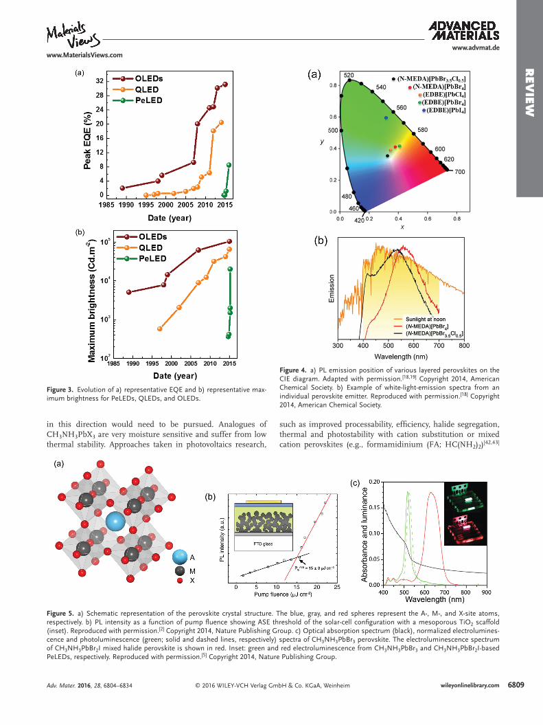
Figure 4. a) PL emission position of various layered perovskites on the CIE diagram. Adapted with permission. [ 18,19 ] Copyright 2014, American Chemical Society. b) Example of white-light-emission spectra from an individual perovskite emitter. Reproduced with permission. [ 18 ] Copyright 2014, American Chemical Society.
Figure 5. a) Schematic representation of the perovskite crystal structure. The blue, gray, and red spheres represent the A-, M-, and X-site atoms, respectively. b) PL intensity as a function of pump fl uence showing ASE threshold of the solar-cell confi guration with a mesoporous TiO 2 scaffold (inset). Reproduced with permission. [ 2 ] Copyright 2014, Nature Publishing Group. c) Optical absorption spectrum (black), normalized electrolumines-cence and photoluminescence (green; solid and dashed lines, respectively) spectra of CH 3 NH 3 PbBr 3 perovskite. The electroluminescence spectrum of CH 3 NH 3 PbBr 2 I mixed halide perovskite is shown in red. Inset: green and red electroluminescence from CH 3 NH 3 PbBr 3 and CH 3 NH 3 PbBr 2 I-based PeLEDs, respectively. Reproduced with permission. [ 5 ] Copyright 2014, Nature Publishing Group.

6810 wileyonlinelibrary.com © 2016 WILEY-VCH Verlag GmbH & Co. KGaA, Weinheim
REV
IEW and [HC(NH 2 ) 2 ] 0.83 Cs 0.17 Pb(I 0.6 Br 0.4 ) 3 ) [ 44 ] would need to be
explored for improved performance of these 3D thin-fi lm light emitters. Besides methylammonium-based perovskites, inor-ganic CsPbBr 3 perovskite thin-fi lm emitters have also yielded stable bright-green emission (407 cd m −2 ) with narrow elec-troluminescence widths and low turn-on voltage. [ 32 ] Improved performance was observed by modulating the precursor stoi-chiometry during thin-fi lm formation with an excess of CsBr (CsBr:PbBr 2 = 2:1) showing nearly 300% improvement in luminescence over the stoichiometric compositions. Besides the increased thermal stability compared to the CH 3 NH 3 PbX 3 family, bulk CsPbBr 3 exhibits other attractive features for light-emitting applications, such as long PL life-time (≈2.5 µs) and electron mobility (≈10 3 cm 2 V −1 s −1 , comparable electron and hole mobility/life-time products, [ 45 ] small exciton binding energy (≈35 meV), [ 46 ] and potentially better ambient stability.
2.1.2. Lower-Dimensionality Layered Perovskites
In contrast to the 3D AMX 3 perovskites, layered perovskites of general formula (RNH 3 ) 2 A n −1 M n X 3 n +1 ( n = 1, pure 2D layered; n = ∞, 3D structure; and n = defi ned integer, quasi-2D layered structure) are formed when cations are introduced that do not fi t in the cuboctahedral cavity between the MX 6 octahedra. The cubic symmetry is broken and the inorganic lead halide layers of the original 3D structure can be separated into <001> or <110> oriented slices or cuts to accommodate the larger cations ( Figure 6 a). Estimated according to the ionic radii of typically used MX 6 constituents Pb 2+ (1.19 Å) and I − (2.20 Å), a layered perovskite structure, of general formula A 2 MX 4 , forms when the ionic radius of the A-constituent exceeds approximately 2.6 Å. [ 24,47 ] The inorganic layers are held together by weak van der Waals forces and are fundamentally different from e.g.,
Adv. Mater. 2016, 28, 6804–6834
www.advmat.dewww.MaterialsViews.com
Figure 6. a) Concept of multidimensionality in perovskite materials; introduction of large organic cations in the inorganic layers break the AMX 3 sym-metry to form perovskites in <110> and <001> oriented A 2 MX 4 layered structures. b) Schematic representation of the bandgap between the valence and the conduction band (VB and CB, respectively) in a 3D perovskite (top) and the bandgap in 2D layered perovskite (bottom). Layered perovskites form a natural quantum well, in which the inorganic sheets and organic molecules act as “well” and “barrier”, respectively. c,d) Intercalation of N 1 -methyl-propane-1,3-diammonium ( N -MPDA) (c) and N 1 -methylethane-1,2-diammonium ( N -MEDA) (d) within the inorganic PbBr 4 2− sheets, resulting in blue-emitting <001> and white-light-emitting <110> oriented structures, respectively. The turquoise, brown, blue, and gray spheres represent Pb, Br, N, and C atoms, respectively. The green spheres represent CH 3 NH 3 + . c,d) Adapted with permission. [ 18 ] Copyright 2014, American Chemical Society. e) Optical absorption spectra of CH 3 NH 3 PbI 3 (black) and (IC 2 H 4 NH 3 ) 2 (CH 3 NH 3 ) n −1 PbnI 3 n +1 perovskite fi lms at different dipping times. Inset: corresponding PL spectra. Reproduced with permission. [ 61 ] Copyright 2015, Wiley-VCH.

6811wileyonlinelibrary.com© 2016 WILEY-VCH Verlag GmbH & Co. KGaA, Weinheim
REV
IEW
metal chalcogenide semiconductors, as here, a rigid backbone is formed through covalent bonds between the metal cations and the Se or S atoms. [ 48 ] In addition, these layered nanostruc-tures can be considered as natural quantum-well structures, where the inorganic layers act as “wells” and the organic mol-ecules as “barriers” (see Figure 6 b). [ 17 ] They possess very large binding energies (several hundreds of meV) due to enhanced electron–hole interactions originating from the very different dielectric constants of the “well” and “barrier”, [ 49 ] while the decreased symmetry diminishes the forbidden electronic tran-sitions and contributes to the enhancement of the photolumi-nescence intensity or quantum yield. As a result of the strong confi nement in two dimensions and wide compositional fl exi-bility, these layered perovskites are ideal for light-emitting appli-cations. [ 18,19,50 ] Moreover, the binding energy is directly tuned by the number of inorganic layers n in the structure, where n = 1 and n = ∞ represent the “pure” layered vs the 3D perovs-kite, respectively (Figure 6 a). Higher-order layered compounds (A′ 2 A n −1 M n X 3 n +2 ) with n = 2, 3, 4, etc. are formed through inter-calation of a mixture of cations, capable of forming both the 3D (A′; e.g., CH 3 NH 3 + , HN = CHNH 3 + , or Cs + ) and layered perovskite structure (A). These compounds can be considered multidimensional, as their dimension lies somewhere between layered 2D and 3D. Although charge transport between the inorganic layers is limited due to the large spacing between the individual layers, vertical-crystal-growth (i.e., inorganic sheets perpendicular to the substrate surface) techniques could help overcome this limitation. [ 17,51 ]
The increased structural freedom creates new possibilities to incorporate larger and more complex structures with tailored photophysical and electronic-transport properties beyond the archetypal perovskite structure, such as conjugated systems with π–π interactions (e.g., phenylethylamines [ 49 ] ), organic dyes (e.g., thiophenes [ 52 ] ), or fl uorophores. However, the nature of the intercalated molecules has implications with respect to the layered structure. For example, hydrogen bonding between the amine and bridging/terminal halides strongly infl uences the orientation and conformation in which the layered per-ovskites are formed. [ 24 ] It has been shown with van der Waals- corrected density functional theory (DFT) calculations; that the orientation of the organic molecules plays a fundamental role in determining the electronic properties of the layered material. [ 53 ] The impact on the structure and properties of the layered perovskite by intercalating various types of organic molecules is discussed below.
Aliphatic, Bifunctionalized, and Cyclic Amines : Aliphatic amines are structurally the simplest organic cations to form layered perovskites (i.e., (C m H 2 m +1 NH 3 ) 2 PbX 4 . The interlayer spacing is directly tuned by the chain length of the amine, and increases monotonically from approximately 4 to 14 Å for m = 4–12, respectively. Despite the increasing interlayer distance, the size of the quantum well remained unchanged, and exciton binding energies of ≈320–420 meV were measured. [ 54,55 ] One of the earlier reports on multidimensionality shows that often thickness-dependent absorption and emission footprints are visible during optical characterization. [ 56 ] For example, methyl-ammonium lead iodide ( n = ∞) has an optical band edge and PL emission around 753 nm. However, introduction of different amounts of decylammonium resulted in the formation of
lower-dimensional layered perovskites ( n = 1, 2, 3 to ∞, respec-tively). Due to strong confi nement in the “pure” layered structure ( n = 1), sharp excitonic absorption bands were observed at much smaller wavelengths than the luminescence band. Higher-order perovskites, on the other hand, displayed multiple absorption maxima at higher wavelengths that were related to their inor-ganic layer thickness. [ 56 ] Similar footprints were observed in PL spectra of layered structures of CH 3 NH 3 PbBr 3 in the presence of octylammonium ligands. [ 57 ] Nanoplates of n = 2 exhibited quantum confi nement, and excitonic absorption blue-shifted approximately 0.5 eV compared to the bulk 3D crystal. Besides changes in the optical properties, changes in electronic proper-ties have also been observed, e.g., on increase of the number of perovskite layers n in (C 4 H 9 NH 3 ) 2 (CH 3 NH 3 ) n −1 Sn n I 3 n +1 , a transition between semiconducting and metallic behavior was displayed. [ 58 ]
Although many of these layered and multidimensional per-ovskites are formed via acid–base reactions, [ 59 ] or slow pre-cipitation from solution-phase, [ 18,19,51,60 ] a different approach has been reported recently. [ 61 ] Multidimensional perovskites were formed by dipping a thin fi lm of “pure” 2D ( n = 1) perovskite (IC 2 H 4 NH 3 ) 2 PbI 4 in a CH 3 NH 3 PbI 3 ( n = ∞) solu-tion in 2-propanol/toluene (Figure 6 e). By controlling the dip-ping time, the dimensionality was tuned between a layered lower-dimensional and bulk 3D perovskite structure, resulting in reduced optical bandgaps (2.02 to 1.62 eV at 0 and 5 min, respectively). At longer dipping times, the absorption bands associated with layered perovskites became less noticeable, indicating an increased stacking of the lead halides lattices. Within 5 min, PL emission similar to CH 3 NH 3 PbI 3 was observed, implying near complete formation of the 3D struc-ture. Recently, it was demonstrated that layered PbBr 2 perovs-kites crystals of N 1 -methylethane-1,2-diammonium ( N -MEDA)[PbBr 4 ] and N 1 -methylpropane-1,3-diammonium ( N -MPDA)[PbBr 4 ] formed <110> and <001> oriented structures (Figure 6 c,d). [ 18 ] Despite the difference of only one carbon in chain length for N -MEDA and N -MPDA and the similarity between the two absorbance spectra, completely different photolu-minescence is observed; the <001> sheets display sharp blue emission at approximately 420 nm, whereas the <110> sheets show broad white-light emission (maximum at 558 nm; PLQY ≈ 0.5%) covering the whole visible spectrum. Crystals with the N -MEDA ligands replaced by EDBE, (ethylenedioxy)-bis-(ethylammonium), yielded “warm” and “cold” white-light-emitting crystals (with a color-rendering index of >84) with quantum effi ciencies of 2 and 9% for the corresponding Cl and Br lead perovskites, respectively. [ 19 ] These single-source emit-ters can potentially replace the the phosphors used in current white-light LEDs. These phosphors often suffer from high effi -ciency losses due to e.g., self-absorption at specifi c wavelengths, as well as changes in the emission color caused by different degradation rates of the individual phosphors. On the contrary, single-source ( N -EDBE)[PbBr 4 ] showed great structural stability, and the color emission and intensity remained unchanged after continuous illumination of more than three months (4 W lamp at 365 nm). [ 19 ] Cyclohexylamine-based (C 6 H 11 NH 3 ) 2 PbBr 4 layered perovskites also display broad white-light emission, albeit it at 90 K, with a PL maximum of 2 eV and full-width half-maximum (FWHM) of ≈660 meV. [ 50 ]
Adv. Mater. 2016, 28, 6804–6834
www.advmat.dewww.MaterialsViews.com

6812 wileyonlinelibrary.com © 2016 WILEY-VCH Verlag GmbH & Co. KGaA, Weinheim
REV
IEW Conjugated Systems and Chromophores : Beyond simple
amines, layered perovskites have also been formed by larger and more complex molecules, such as conjugated molecules and chromophores. The π–π interactions within and between the molecules strongly infl uence the ordering (conformation and orientation) between the inorganic layers. For example, well-ordered inorganic CuX 6 octahedral layers are formed in (C 6 H 5 (CH 2 ) 2 NH 3 ) 2 CuX 4 (X = Br − or Cl − ), in which the ammonium groups are hydrogen bonded to the halides, while distorted lay-ered structures are formed with PbCl 6 -based perovskites. [ 24,52 ] In addition, the optical performance is strongly dependent on the chain length of the R-group in R–NH 3 + . [ 62,63 ] A fi ve-fold PL increase was observed in (C 6 H 5 (CH 2 ) m ) 2 PbBr 4 by changing m from 1 to 2. A further increase to m = 3 resulted in only ≈22% of original value of m = 1. In one of the early reports, large single-crystalline (PEA) 2 PbI 4 grown from solution displayed green EL emission at low temperatures. Via a spray-casting method, 50–500 nm-sized layered crystals were formed exhibiting green emission at similar wavelengths as single crystals. [ 64 ] Although the particle size was much larger than the exciton Bohr radius, quantum confi nement originating from the layered structure was observed (interlayer spacing ≈1.6 nm). As opposed to the large layered structures formed via self-organization, fi lm depo-sition from solution is more convenient, while the stability of the layered perovskite is retained.
The accommodation of the double-protonated 5,5′′′-bis(2-aminoethyl)-2,2′:5′,2′′:5′′,2′′′-quaterthiophene (AEQT) chromo-phore in between the PbBr 4 2− sheets results in a <001> ori-ented structure that exhibits green photoluminescence. Unlike the straight confi guration of the organic molecules in C 6 H 5 (CH 2 ) 2 NH 3 ) 2 CuX 4 , the dye molecules are arranged in a her-ringbone-type confi guration, where the amines are hydrogen-bonded to both bridging and terminal halides. [ 52 ] Devices from thick layered perovskites (300 nm) displayed bright-green emis-sion with a maximum effi ciency of 0.1 lm W −1 (at 8 V). [ 30 ] Ori-ented layered fi lms using other chromophores such as naph-thalene and azobenzene have also been reported. [ 65 ] These are interesting materials, as the excited states of the chromophores are higher in energy than the inorganic layers, and thus the emission originates from the inorganic backbone.
2.2. Nanostructured Perovskites
One of the major advantages over traditional inorganic oxides is the low energy barrier to form organic–inorganic hybrid per-ovskites, where a crystalline phase is readily obtained by merely mixing and grinding the precursor salts at room temperature. Although this method suffers from lack of precise experimental control, it exemplifi es the ease with which the organic cations can diffuse into the inorganic framework. Typically, perovskite synthesis is performed via wet-chemistry routes, allowing for mixing at a molecular level, and resulting in materials with high phase purity. By carefully controlling the reaction condi-tions (e.g., temperature, solvent, ligands), hybrid perovskites of various morphologies (0D quantum dots to 3D single crystals) and sizes (stretching 6 orders of magnitude) can be prepared ( Figure 7 ). Nanostructuring can be achieved in both layered and 3D perovskites. For example, CH 3 NH 3 PbBr 3 single-crystals
(bulk) with a size of 5 mm × 5 mm × 2 mm are formed within several hours by exploiting its lower solubility in solvents at elevated temperatures, [ 66 ] and CH 3 NH 3 PbBr 3 nanoparticles (NPs), [ 34,67–69 ] layered sheets, [ 36,57 ] and nanowires (NWs) [ 70,71 ] have also been formed (Figure 7 b–e).
These examples only briefl y showcase the ease at which a wide variety of nanostructured perovskites can be obtained. In recent years, nanostructuring of materials has become increas-ingly important, as certain phenomena (absent in bulk mate-rials) are only observed at the nanoscale. The material’s proper-ties are directly tuned during synthesis and are closely related to their size (and size distribution). For example, judicious control over the synthesis conditions (e.g., precursor concentra-tion, reaction temperature, choice of ligands, etc.) may result in different optical properties originating from, for example, quantum size effects [ 16 ] or anisotropic particle growth. [ 72 ] The typical synthetic strategies toward organic–inorganic hybrid perovskites, and the effect on the material’s photophysical and morphological properties, will be discussed below (color-tuna-bility is discussed in a subsequent section).
2.2.1. Nanoparticles (NPs) and Quantum Dots (QDs)
Currently, most reported synthetic routes leading to the forma-tion of hybrid perovskite nanoparticles (NPs) can be divided into two distinct strategies. CH 3 NH 3 PbX 3 NPs are predomi-nantly formed using the ligand-assisted reprecipitation method (LARP). Polar solvents, capable of dissolving the inorganic lead and ammonium halide (MA-X) salts, are injected into a non-polar “poor” solvent in the presence of coordinating ligands to stabilize the newly formed particles. Due to the tempera-ture instability, these syntheses are conducted at low tempera-tures (<80 °C). [ 16,34,67–69,73,74 ] Alternatively, replacement of the CH 3 NH 3 + cation with Cs + yields inorganic perovskites with increased structural stability. These inorganic CsPbX 3 NPs are prepared using a hot-injection method at temperatures in excess of 150 °C. The NPs are typically formed by swiftly injecting Cs-oleate, formed through reaction between Cs 2 CO 3 and oleic acid (OA), in a solution of PbX 2 (X = Cl − , Br − , or I − ) in non-coordinating solvents (such as 1-octadecene; ODE) at temperatures ranging 140–200 °C under N 2 atmosphere [ 15,75–77 ] Here, the presence of OA and oleylamine (OAm) ligands help to inhibit the crystal growth, passivates the surface defects, and contributes to colloidal stability. This method has been suc-cessfully employed in the fabrication of high-quality inorganic semiconductor NPs. [ 78 ] One of the remarkable features of the hybrid perovskites is that, as opposed to semiconductor QDs, no additional surface passivation was necessary to achieve a high PLQY, and dangling bonds (from surface ligands) did not play a role in the PL emission. [ 15,76 ]
Colloidal CH 3 NH 3 PbBr 3 cubic nanoparticles (≈6 nm) using the LARP method (Figure 7 b) [ 34 ] were precipitated (at 80 °C) in the presence of long-chain ammonium bromide ligands, and exhibited bright-green PL emission at 527 nm, with a PLQY of approximately 20%. Increased reaction temperatures (120 °C), yielded equal quantum effi ciencies and PL emission wave-lengths, [ 79 ] showcasing the rigidity and high reproducibility of the method. The synthesis was further optimized by increasing
Adv. Mater. 2016, 28, 6804–6834
www.advmat.dewww.MaterialsViews.com

6813wileyonlinelibrary.com© 2016 WILEY-VCH Verlag GmbH & Co. KGaA, Weinheim
REV
IEW
the organic/inorganic precursor ratios and narrow PL emis-sion (FWHM ≈ 30 nm, at 520 nm), and signifi cantly improved PLQY values of 83% were recorded. [ 67 ] The improvement stems mainly from better surface passivation by the ligands. Quantiza-tion effects were observed for 1.8–3.6 nm-sized CH 3 NH 3 PbBr 3 NPs prepared at 0–60 °C, respectively; accompanied by blue-shifted PL emission at 475, 500, and 520 nm. [ 68 ] Especially at low temperatures, ligands will most likely stay on the surface of the NPs, strongly affecting their growth. [ 80 ] Although the highest PLQY to date (93%) was recorded, the effect may also be attributable to size-exclusion from the very high centrifugation speeds (14 500 rpm) used. In addition, only the supernatant phase (containing only the smallest NPs) was used, instead of the precipitate. [ 34,67 ] Nanoparticles of CH 3 NH 3 PbBr 3 (≈3.3 nm)
have also been reported utilizing n -octylamine (OLA) as the surface capping ligand, with the supernatant colloidal solution exhibiting high PLQY (≈50–70%). [ 69 ] A small degree of quantum confi nement was suggested with a blue-shifted PL emission at ≈515 nm. The PL life times of these NPs (≈6–24 ns) [ 68,69 ] are signifi cantly lower than in bulk CH 3 NH 3 PbBr 3 (≈100 ns), [ 81 ] indicating that PL decay predominantly originates from radia-tive exciton recombination.
Despite the high quantum yields and colloidal stability of methylammonium halide NPs (>5 months in air under dark conditions [ 67 ] ), a major shortcoming arises from its instability in polar solvents (also used to dissolve the precursors prior to NP formation). To overcome this, Vybronyi et al. synthesized CH 3 NH 3 PbX 3 without the use of polar solvents. [ 82 ] Although
Adv. Mater. 2016, 28, 6804–6834
www.advmat.dewww.MaterialsViews.com
Figure 7. a) Schematic representation of the hybrid-perovskite phase formation and the resulting morphologies. b) Green photoluminescence of 6 nm-sized CH 3 NH 3 PbBr 3 NPs. Inset: High-resolution TEM (HRTEM) image of individual nanoparticle (scale bar 2 nm). Adapted with permis-sion. [ 34 ] Copyright 2014, American Chemical Society. c) Top: Photograph of colloidal 2D organo-lead iodide perovskite NC solutions under ambient light of (from left to right) n = 1, 2, and 3, respectively. Bottom: schematic structures of the colloidal 2D organo-lead iodide perovskites NPs (C 18 H 35 NH 3 ) 2 (CH 3 NH 3 ) n −1 [Pb n I 3 n +1 ], where (from left to right) n = 1, 2, and 3. Reproduced with permission. [ 33 ] Copyright 2015, Wiley-VCH. d) Absorb-ance and photoluminescence spectra of chemical-vapor-deposited CH 3 NH 3 PbI 3 NPLs on a mica substrate. Inset: optical images of NPLs; the optical contrast corresponds to different NPL thickness. Adapted with permission. [ 36 ] Copyright 2014 American Chemical Society. e) CsPbBr 3 NWs formed through the self-assembly of nanocubes after 90 min of reaction. Adapted with permission. [ 35 ] Copyright 2015, American Chemical Society.

6814 wileyonlinelibrary.com © 2016 WILEY-VCH Verlag GmbH & Co. KGaA, Weinheim
REV
IEW the precipitate displayed lower quantum effi ciencies (25–50%)
than previously reported for CH 3 NH 3 PbBr 3 NPs, it shows that an alternative synthesis route without the use of polar solvents is possible. Other approaches involved the formation of PbS/CH 3 NH 3 PbX 3 core–shell NPs via ligand-exchange reactions, in which the halide successfully passivated the surface traps on the PbS nanoparticle surface. [ 83,84 ] Light emission associated with charge transfer between PbS/CdS NPs and CH 3 NH 3 PbI 3− x Cl x has also been reported. [ 85 ]
Beyond the methylammonium perovskite family of mate-rials, color-tunable CsPbX 3 perovskite NPs (4–15 nm diam-eter) using the hot-injection method at temperatures ranging 140–200 °C ( Figure 8 a) have also been reported. [ 15 ] The resulting NPs exhibited very high quantum yields of 50–90% and narrow emission line widths of 12–42 nm. Owing to the large Bohr radius calculated for CsPbCl 3 (5 nm), CsPbBr 3 (7 nm), and CsPbCl 3 (12 nm), quantum confi nement was observed. [ 15 ] With transient absorption spectroscopy (TA), it was determined that the high quantum yields arise from negligible electron–hole trapping pathways, [ 86 ] and an average PL life-time of τ = 1–29 ns was recorded, with the lowest value for CsPbCl 3 (≈1 ns; PLQY ≈ 50%). [ 15,77,86 ] Unlike semiconductor QDs, no spectral broad-ening originating from the high surface trap densities (due to the large surface-to-volume ratio), or size-distribution, was observed. [ 77 ] In addition, CsPbX 3 does not show changes in optical bandgap at elevated temperatures, which is important for color quality retention in light-emitting devices (i.e., heating effects). [ 77 ]
2.2.2. Nanoplates (NPLs)
Currently, NPLs have not been extensively used in optoelec-tronic devices, and there is only one published report on their use in light-emitting devices. [ 87 ] However, signifi cant efforts have been made to synthesize these nanosized materials for increased photoluminescence quantum yield and structural stability. Besides the use of long-chain ligands to form lower-dimensionality layered perovskites along (100) slices and (110) cuts of the 3D structure, they can also be used to selectively inhibit the crystal-growth direction in one dimension. Thin quasi-2D perovskites are then formed by morphological control, rather than by separation of the individual inorganic layers. [ 87 ]
Formation of 1.2 nm-thick CH 3 NH 3 PbBr 3 NPLs was dem-onstrated via non-templated routes and, [ 57 ] although PL emis-sion could not be observed due to the low concentration of NPLs, the absorption peak at 431 nm was blue-shifted ≈0.5 eV compared to that in the bulk. [ 56,88 ] Additional absorp-tion maxima at 431, 451, 472, and 525 nm, corresponding to n = 1, 3, 4, and ∞, respectively, were in agreement with earlier reports for layered perovskites. [ 56,59 ] Similarly, changes in the size, morphology, and PL emission were observed by adjusting the ratio between methylammonium and octylammonium cat-ions [ 16,73 ] The blue-shifts originating from quantum confi ne-ment are partially counteracted due to the high binding energy (several hundred meV) found for NPLs of n < 3. [ 16 ] The calcu-lated excitonic Bohr radius of 1.36 nm is in agreement with the estimation of Tyagi et al. (1.4–2 nm) [ 57 ] and corresponds to a platelet thickness between n = 2–3. [ 16 ] This corroborates with
earlier fi nding, where confi nement for n = 2 structures was observed. [ 56 ]
Tuning of the morphology of CH 3 NH 3 PbX 3 (X = Br − or I − ) NPs from nanocubes to NPLs and NWs, was achieved by adjusting the ratio between the OAm and OA ligands. [ 82 ] The CH 3 NH 3 PbBr 3 nanoplates exhibited blue PL emission and absorption at 465 and 450 nm, respectively, with a PLQY of ≈18%. Self-organization of these platelets led to the forma-tion of wire-like structures, with green PL emission at 530 nm (PLQY ≈ 15%). Similar asymmetric growth and self-assembly in hierarchical structures was observed by controlling the reac-tion temperature of the CsPbBr 3 NC synthesis. [ 15 ] Instead of green-emitting nanocubes (8–10 nm; formed at >150 °C), reac-tions at 130 and 90 °C yielded cyan- and blue-emitting NPLs, respectively. The remarkably high quantum yields (up to 84%) indicate a low concentration of surface defects. [ 89 ]
Beyond NPLs of 3D materials (e.g., CH 3 NH 3 PbBr 3 , CsPbBr 3 ) atomically thin, uniformly square-shaped sheets of layered perovskite (CH 3 (CH 2 ) n NH 3 ) 2 PbBr 4 ( n = 3 and 7) have also been prepared. [ 16,48 ] A ternary solvent was employed to facili-tate controlled precipitation of NPLs and utilizing the different precursor solubility in each solvent. [ 48 ] The thinnest sheets (≈1.6 nm) showed deep-blue PL emission at 406 nm and PLQY of ≈26%, compared with <1% in the bulk crystal, which was attributed to quantum confi nement effects. [ 48 ] For layered (CH 3 (CH 2 ) 7 NH 3 ) 2 PbBr 4 , slightly red-shifted PL emission (at 427 nm) was observed, which can be explained by the reduced confi nement from the larger effective spacing between the inor-ganic layers. [ 16 ] Although ligands can effectively help “steer” the reaction and morphology of the perovskites, post-processing and purifi cation steps are necessary for thin-fi lm formation. To overcome this problem, Yuan et al. described a one-pot synthesis approach using a mixture of PbBr 2 , HBr, OLA, and benzyl amine in dimethylformamide (DMF), which circum-vented the pre-preparation of ammonium salts and ligands. [ 90 ] The formed NPLs, with thicknesses and lengths of 100–150 nm and 1–4 µm, respectively, showed narrow PL emission ranging 403–413 nm, with a PLQY of ≈53%. Quantum yields as high as 85% were obtained when smaller methyl amine was used, instead of benzyl amine. [ 87 ] In addition, the non-radiative decay was lower the radiative decay (PL life-time 3.1–4.7 ns; approxi-mately two times faster than NPs), indicating minimal surface and self-quenching effects. [ 90 ]
The general strategy in the above-mentioned methods is based on the direct formation of the nanoplates. The precursors are pre-mixed in a “good” solvent, and NPLs are subsequently precipitated from solution. However, transformation via an intermediate phase has also proven very successful. Not only can the hybrid perovskite phase form, the pre-existing mor-phology of the seed can also be retained. Hassan et al. dem-onstrated this concept and synthesized highly luminescent 5.5 nm-sized CH 3 NH 3 PbX 3 layered halide perovskites (PLQY ≈ 20%) from seeded PbX 2 NPs (X = Br − or I − ) (see Figure 7 c). [ 33 ] The PL emission at 505, 565, and 600 nm was tuned by control-ling the thickness of the layers to n = 1, 2, and 3 using long-chain ligands. Quantization due to spatial confi nement was observed, despite the NPs sizes being larger than the reported Bohr radius, [ 16,57 ] Similarly, Zhang et al. formed CH 3 NH 3 PbX 3 NPLs from pre-formed PbX 2 (X = Cl − , Br − , or I − ) platelets using
Adv. Mater. 2016, 28, 6804–6834
www.advmat.dewww.MaterialsViews.com

6815wileyonlinelibrary.com© 2016 WILEY-VCH Verlag GmbH & Co. KGaA, Weinheim
REV
IEW
Adv. Mater. 2016, 28, 6804–6834
www.advmat.dewww.MaterialsViews.com
Figure 8. a) Colloidal CsPbX 3 (X = Cl − , Br − , and I − ) perovskite NPs solutions with tunable bandgap energies covering the entire visible spectrum. Top: colloidal NPs solutions in toluene under UV lamp illumination ( λ = 365 nm). Bottom: representative PL spectra. b) Typical PL and optical absorption spectra of colloidal solutions from (a); a,b) reproduced with permission. [ 15 ] Copyright 2015, American Chemical Society. c) In situ PL measurement of CsPbBr 3 to CsPbI 3 conversion at 40 °C using [Br] parent /[I] incoming = 1:3; c) Reproduced with permission. [ 76 ] Copyright 2015, American Chemical Society. d) Schematic representation of interparticle anion exchange (Panel 1) and optical absorption and PL spectra of various CsPb(Cl:Br) 3 and CsPb(Br:I) 3 NPs prepared via interparticle anion exchange (Panel 2). TEM images of mixed CsPbBr 3 :CsPbCl 3 (1:1) and CsPbBr 3 :CsPbI 3 (1:1) NPs (Panel 3 and 4, respectively). The scale bars correspond to 50 nm. Reproduced with permission. [ 75 ] Copyright 2015, American Chemical Society. e) Photographs of colloidal solutions in toluene with varying octylammonium content under a UV lamp (top) and TEM images of NPLs and NPs prepared with 80% and 0% octylammonium, respectively (bottom). Reproduced with permission. [ 16 ] Copyright 2015, American Chemical Society.
6816 wileyonlinelibrary.com © 2016 WILEY-VCH Verlag GmbH & Co. KGaA, Weinheim
REV
IEW vapor-phase deposition (Figure 7 d). [ 36 ] Lead halide platelets
were converted to the corresponding CH 3 NH 3 PbX 3 phase by evaporation of a MA-X source, while maintaining the hexagonal lead halide geometry. Despite a PLQY ≈ 17%, the high binding energy (45 ± 11 meV), long diffusion lengths, and PL life-time of ≈2.6 ns demonstrate that these NPLs have favorable proper-ties for effi cient light-emission.
2.2.3. Nanowires (NWs) and Nanorods (NRs)
One-dimensional structures have attracted considerable atten-tion due to their high surface-to-volume ratio and structural anisotropy. For this reason, they are often employed in sensing and catalysis applications. To date, only a few reports have been published on the preparation of halide perovskite NWs for LED, [ 35,70 ] lasing, [ 3,71 ] and photodetector [ 91 ] applications. For example, photoluminescent CH 3 NH 3 PbX 3 and CsPbX 3 (X = Cl − , Br − , or I − ) NWs have been demonstrated. [ 35,70,71 ] The CH 3 NH 3 PbBr 3 NRs were grown directly on poly(3,4-ethylen-edioxythiophene) polystyrene sulfonate (PEDOT:PSS)-coated indium-doped tin oxide (ITO)/glass substrate by converting lead acetate NWs via immersion in a CH 3 NH 3 Br solution. [ 70 ] Green PL and EL emission (at ≈533 nm) was demonstrated from a light-emitting array of NWs, indicating good electron and hole injection. Single-crystalline CsPbX 3 NWs (12 nm width and lengths up to 5 µm; Figure 7 e) formed sequentially through the assembly of nanocubes [ 35 ] at prolonged reaction times using the method described by Protesescu et al. [ 15 ] A similar type of self-organization of CH 3 NH 3 PbX 3 (X = Br − or I − ) and CsPbBr 3 of nanoplates into larger wire-like structures was observed. [ 82,89 ] The CsPbBr 3 NWs showed a small degree of confi nement, as a 60 meV blue-shift was observed in the PL spectra.
2.4. Color Tunability
Halide perovskites enjoy great structural fl exibility, and their morphology can be conveniently manipulated during synthesis, resulting in a wide variety of shapes and sizes. The bandgap in these perovskites can be tuned by, for example, (partial) sub-stitution of the cation or by changing the halide source during synthesis. This strategy has already been exploited in photo-voltaic devices, and mixed-cation and mixed-halide perovskites have already been synthesized for better stability and optimal bandgap. [ 44 ] Although for single-junction solar-cell applications a small-bandgap material is required for high effi ciency, this is not a prerequisite for light-emitting devices or good light emis-sion in general. Instead, materials with PL emission across the visible spectrum with narrow emission line-widths and limited spectral overlap are required.
2.4.1. Anion-Based Color-Tuning
Hybrid perovskites have already demonstrated that variation of the anion in, for example, CH 3 NH 3 X 3 (Cl − , Br − , or I − ), tunes the bandgap from 3.11 eV, to 2.3 eV, and 1.55 eV, respectively. [ 92 ]
Color-tuning by partial halide substitution during the perov-skite synthesis has proved successful, irrespective of the reac-tion conditions (e.g., temperature), reaction media (i.e., solution and thin fi lms), cationic nature (i.e., CH 3 NH 3 PbX 3 or CsPbX 3 ), or sample morphology (e.g., NPs, nanoplates, or NWs). For example, the PL emission of CsPbX 3 NPs could be tuned across the whole visible spectrum (Figure 8 a,b). The use of different halide sources yielded NPs of high quantum yield and high color-purity with narrow PL emission at approximately 410 nm (X = Cl − ), 525 nm (X = Br − ), and 700 nm (X = I − ), covering a wide color gamut. [ 15 ] The use of different halide stoichiometry yields PL emission exactly in between the expected values for the “pure” perovskite NPs (see Figure 8 a,b).
This color-tuning approach was extended by exploiting the ionic nature of the hybrid perovskites, in particular the high mobility of halides. Anions could be replaced in situ by sub-jecting pre-formed NPs (or thin fi lms) to anion-exchange reactions. [ 75,76,93 ] For example, anion-exchange was initiated by swiftly injecting a different halide precursor to purifi ed CsPbBr 3 NPs in toluene at temperatures of <40 °C. In most cases, the anion exchange proceeds rapidly, and is fi nished within seconds. Throughout the exchange reaction, a gradual shift in PL emission can be observed (Figure 8 c). The fi gure shows time-resolved PL emission and intensity during the exchange reaction from CsPbBr 3 to CsPbI 3 , in which an excess of oleylammonium iodide (3:1) is added to CsPbBr 3 NPs. Immediately after injection, the PL emission shifted to higher wavelengths due to the formation of iodide-rich domains. This rapid color change was also observed in the transformation of thin-fi lm CH 3 NH 3 PbBr 3 to CH 3 NH 3 PbI 3 , although prolonged reaction times were necessary to form a homogeneous solid solution. [ 93,94 ] By carefully adjusting the ratios of the incoming and parent halide, the PL emission was tuned across the whole visible range (≈410–690 nm). [ 75,76 ] Exchange reactions were possible between all halide combinations, except Cl − and I − , due to the large difference in ionic radii (1.81 Å and 2.20 Å, respectively) and lattice mismatch of the parent perovskites phases. From X-ray diffraction (XRD) and microscopy studies, it was also observed that not only the morphology of the parent perovskite NPs remains unchanged after anion exchange, but also the initial crystal structure is also retained. [ 75,76 ] Cubic CsPbI 3 NPs were prepared from cubic CsPbBr 3 through anion exchange, resulting in highly luminescent NPs, whereas direct synthesis yields the non-luminescent orthorhombic phase. [ 76 ] Although a cubic-to-tetragonal phase transition was observed for iodide-exchanged CH 3 NH 3 PbBr 3 NPLs due to the larger ionic radius of iodide compared to bromide, the morphology was unaffected. [ 93 ] On the contrary, both the single-crystalline tetragonal structure and the morphology of CH 3 NH 3 PbBr 3 NWs were retained after vapor-phase halide exchange with CH 3 NH 3 I at 150 °C. [ 70 ] The concept of facile exchange reactions has been further demonstrated through the cross-exchange of halides from discrete NPs (see Figure 8 d). [ 75,76 ] Simply mixing e.g., the pure CsPbBr 3 and CsPbI 3 NPs initiates exchange reactions, and instantaneous red and blue shifts are observed in the PL spectra, respectively. Full exchange occurs within 20 min, and a single PL peak indicates that the halides are homogeneously distributed within NPs (i.e., CsPbBr 1.5 I 1.5 ; Figure 8 d panel 2), [ 75 ] and the PLQY, PL emission, and PL line
Adv. Mater. 2016, 28, 6804–6834
www.advmat.dewww.MaterialsViews.com
6817wileyonlinelibrary.com© 2016 WILEY-VCH Verlag GmbH & Co. KGaA, Weinheim
REV
IEW
widths are equivalent to those obtained from direct synthesis or direct halide exchange. [ 76 ]
Although the ease with which halide exchange takes place can be exploited to tune the emissive colors of NPs or thin fi lms, it poses severe problems when fi lms of different halide composition are stacked. Halide “leeching” was observed when Br − (green emission) and I − (red emission) containing fi lms were deposited sequentially, with subsequent loss of the individual PL emission. [ 73 ] Anion-exchange was inhibited by embedding the NPs in a polymer matrix, and no signifi cant shift in PL emission was observed for both fi lms. By employing this strategy, green- and red-emitting fi lms were deposited on a blue-emitting GaN chip, and white-light emission from perov-skite NC fi lms was demonstrated. [ 73 ]
2.4.2. Cation-Based Color-Tuning
The halide exchange reaction enables tunability of the PL emis-sion to any desired wavelength across the visible spectrum. Cation substitution can also be employed to tune the wave-length of nanostructured perovskites, [ 16,73,95 ] although usually on a much smaller wavelength range. Cation substitution is used as a common strategy to change the color emission, e.g., Ag 2 Se NPs and PbS NRs from CdSe NPs and CdS NRs, respec-tively. [ 96,97 ] Similar to the halide exchange in perov skites, [ 75,76 ] the pre-existing morphology can be preserved after cation sub-stitution. Cation substitution of CsPbBr 3 NPs with CH 3 NH 3 + cations from methylammonium bromide (MA-Br) [ 75 ] resulted in a PL shift from 510.2 to 525.4 nm, similar to the PL value (527 nm) observed for CH 3 NH 3 PbBr 3 . [ 34 ] A slight lattice expan-sion observed in the XRD patterns would further support the replacement of Cs + with the larger CH 3 NH 3 + cations. [ 75 ] Although octylammonium bromide (OA-Br) has signifi cantly improved the PLQY of CH 3 NH 3 PbBr 3 NPs by effectively pas-sivating the surface and inhibiting crystal growth, [ 67 ] increased concentrations result in blue-shifts in the PL emission due to the concurrent formation of lower-dimensional layered perov-skites (Figure 8 e). [ 16,73 ] At low MA-Br:OA-Br ratios (<40% OA-Br) the PL emission remains virtually unchanged (517–519 nm); however, rapid blue-shifts are observed at higher ratios. At ratios <40%, OA-Br still acts as a capping ligand, restricting the growth of the formed NPs. This is supported by transmission electron microscopy (TEM) observations, as predominantly small crystals are formed. [ 16,73 ] At ratios >60% OA-Br, multiple maxima originating from both mixed (MA/OA)PbBr 3 NPs and layered (OA) 2 PbBr 4 perovskites are observed in the absorption spectra, [ 73 ] and lower quantum yield are recorded.
2.5. Integration of Perovskite Emitters into Light-Emitting Devices
Although halide perovskites exhibit remarkable optoelectronic properties, their integration into functional light-emitting devices requires further consideration. The combination of strong photoluminescence (up to 70% at high photon fl uxes) [ 31 ] and good electroluminescence properties in solar-cell-device confi guration [ 4,98 ] has projected the organic–inorganic halide
perovskite material as a perfect candidate for PeLEDs. Besides the emitter materials, the choice of matching electron- and hole-transporting materials and their integration into a light-emitting device are critical to defi ne the device characteristics. To minimize energetic mismatch and minimize non-radiative recombination, multilayered device structures and optimization of a plurality of interfaces would be essential to leverage the material’s full potential.
Due to the attractive merits, such as large absorption coef-fi cients, ultralow bulk defect densities, slow Auger recombina-tion, and long-range carrier diffusion length, hybrid perovskite materials are also considered as a new class of optical-gain media for lasing applications. The easy solution processability at low temperature means that this kind of materials can be embedded into a wide range of cavity resonators, which is attractive for the realization of on-chip coherent light sources. However, despite the success in achieving optically pumped hybrid perovskites lasers with relatively low pump fl uence threshold, electrically driven lasers remain a signifi cant chal-lenge and have not been realized yet. Many challenges, such as fulfi lling the requirements of higher injection current densi-ties, lower carrier threshold, and lower heating effects, need to be overcome in the future.
3. Light-Emitting Devices
This section addresses the use of perovskites for lighting appli-cations. As the main device concept, PeLEDs rely on electrical charge injection, transport, and radiative recombination. The role of the various device components, as well as the different reported device architectures will be discussed in this section. Other device confi gurations based on perovskites, such as light-emitting transistors and light-emitting electrochemical cells, are also considered. In the last subsection, the working mecha-nisms and performance losses will be analyzed.
3.1. Perovskite Light-Emitting Diodes
In general, the PeLED device architectures consist of a front trans-parent electrode (e.g., FTO, ITO), electron-transporting layer (ETL) material (e.g., TiO 2 , ZnO, poly(9,9-dioctylfl uorene) (F8), 2,2′,2″-(1,3,5-benzinetriyl)-tris(1-phenyl-1-H-benzimidazole) (TPBi), bathocuproine (BCP), etc.), emitter, hole-transporting layer (HTL) material (e.g., PEDOT:PSS, poly(9,9-dioctyl-fl uorene- co - N -(4-butylphenyl)diphenylamine) (TFB), 2,2 ′ ,7,7 ′ -tetrakis-( N,N -di-4-methoxyphenylamino)-9,9 ′ -spirobifluorene (spiro-MeOTAD), poly( N , N ′-bis(3-methylphenyl)- N , N ′-diphenyl-benzidine) (polyTPD), etc.), and back electrode ( Figure 9 ). The PeLED architecture may be generalized as ETL/perovskite/HTL and HTL/perovskite/ETL confi gurations; with the generated light transmitting through the ETL and transparent electrode for the former and through the HTL for the latter ( Figure 10 b,c). Ideally, the carriers that are injected through the electrode should be transported effi ciently to the emitter, and confi ned to promote radiative recombination (i.e., electroluminescence). Losses may include both electrical and optical and, in addition to the emitter material, the design and selection of the inter-faces are critical for high-performance devices. Detailed device considerations including processing of the emitter materials,
Adv. Mater. 2016, 28, 6804–6834
www.advmat.dewww.MaterialsViews.com

6818 wileyonlinelibrary.com © 2016 WILEY-VCH Verlag GmbH & Co. KGaA, Weinheim
REV
IEW
selection and integration of the ETL and HTL, the working mechanisms of LEDs, and, fi nally, losses are discussed in detail in subsequent sections.
3.1.1. Tailoring the Band Alignment of the Interfacial Layer ( i.e., HTL and ETL)
A device is only as effi cient as the interfaces that inject the charges and the multilayered structures that facilitate out-cou-pling of light. In this context, it is the interface that defi nes the device; and, in particular, the choice of appropriate ETL and HTL is of critical importance to the device effi ciencies. The selection of the ETL and HTL is governed by the energy band alignment (to inject the carrier in the emitter) and by the materials’ chemical compatibility (this includes consid-erations on the solvents, in the case of solution processed devices). Naturally, an HTL with electron-blocking ability (i.e., low electron affi nity) or an ETL with hole-blocking ability (i.e., deep valence-band energy) is preferred for an effi cient PeLED.
Successful high-effi ciency demonstrations in solar cells has fueled interest in perovskites for light-emission applications. Thus, the early reports on 3D perovskite PeLEDs employed the basic device structure from solar cells, with CH 3 NH 3 PbI 3 perovskite infi ltrated into mesoporous TiO 2 , [ 4 ] with spiro-OMeTAD functioning as the HTL and the ITO and TiO 2 pro-viding the electron-injecting contact and the ETL, respectively (Figure 10 a). Signifi cant electroluminescence (7.1 W sr −1 m −2 ), EQE (0.48%), and exceptionally low turn on voltage (compa-rable to the emitter bandgap, i.e., 1.5 eV) was shown with this approach. [ 4,5 ] Despite the lack of carrier-confi nement capability in the solar-cell confi guration, the superior EQE and low turn-on voltage suggested signifi cantly low non-radiative losses of the materials. When CH 3 NH 3 PbI 3 was substituted with CH 3 NH 3 PbBr 3 , the bandgap and consequently the emission wavelength of the PeLED could be altered to the visible region (i.e., 2.5 eV). [ 99 ]
Inorganic oxide semiconductor materials (i.e., ZnO, TiO 2 ) have signifi cant advantages when employed as the ETL, such as their stability to moisture and thermal effects. However,
Adv. Mater. 2016, 28, 6804–6834
www.advmat.dewww.MaterialsViews.com
Figure 9. Energy levels for different materials acting as electron-transporting layer (left), thin-fi lm 3D perovskite emitter (middle) and hole-transporting layer (right) in PeLEDs.
Figure 10. a) Schematic diagram and cross-sectional images of PeLED adapted from solar-cell confi guration using mesoporous TiO 2 and spiro-MeOTAD as the ETL and HTL respectively. Reproduced with permission. [ 4 ] Copyright 2015, American Chemical Society. b,c) Schematic representation of PeLED architecture with HTL/perovskite/ETL (b) and ETL/perovskite/HTL (c) confi guration.
6819wileyonlinelibrary.com© 2016 WILEY-VCH Verlag GmbH & Co. KGaA, Weinheim
REV
IEW
their electron affi nity is considerably high, which can hinder the electron injection to the emitter, especially when a high-bandgap CH 3 NH 3 PbBr 3 emitter is used. Surface modi-fi ers can be introduced to initiate the formation of surface dipoles and consequently increase the work function of the oxide semiconductor to facilitate better carrier injection in to CH 3 NH 3 PbBr 3 . Ethanolamine (EA) can be employed as a com-pact TiO 2 surface modifi er, resulting in an increase of 0.3 eV in the TiO 2 work function. The use of EA as a compact TiO 2 surface modifi er (ITO/TiO 2 /EA/CH 3 NH 3 PbBr 3 /SPB-02T/MoO 3 /Au) resulted in a reduction of the turn-on voltage from 4.5 V to 3.5 V and an enhancement of the EQE from 0.026% to 0.051% at 5.8 V. [ 99 ] Efforts to further enhance the EQE were focused on increasing the electron mobility by using ZnO as the ETL, and facilitating charge injection into the emitter by lowering the work function of the ETL through surface modifi ers (e.g., poly(ethylenimine) (PEI)), and using an HTL with a high electron affi nity (TFB) to block the elec-tron fl ow. These device architectures ( Figure 11 a) resulted in brightness and EQE as high as 28 W sr −1 m −2 and 3.5% at 2.2 V for devices with CH 3 NH 3 PbI 3 as the emitter. [ 100 ] When CH 3 NH 3 PbBr 3 was employed as the emitter, an EQE of 0.8% with brightness of 20 000 cd m −2 could be attained at 2.8 V (Figure 11 b). The turn-on voltages of these devices are comparable with the bandgap of the emitter (i.e., 1.5 eV and 2.5 eV for CH 3 NH 3 PbI 3 and CH 3 NH 3 PbBr 3 , respectively). [ 100 ] The emission spectra with various applied voltage are also consistent with the emitter bandgap (Figure 11 c). The high brightness at signifi cantly low voltage indicates small energy loss from carrier transport and carrier injection to the emitter, as well as superior carrier confi nement in the emitter layer.
On the other hand, the fi rst report of electroluminescence with the HTL/perovskite/ETL confi guration was on the ITO/PEDOT:PSS/emitter/poly(9,9-dicotylfluorene)(F8)/Ca/Ag structure, which resulted in turn-on voltages of 1.5 V and 3.3 V with EQEs of 0.23% and 0.1% for CH 3 NH 3 PbI 3 and CH 3 NH 3 PbBr 3 respectively. [ 5 ] Due to the formation of on-chain keto defects in F8 under applied bias in air, atomic layer dep-osition of Mg doped ZnO could be an alternative to improve device stability. Mg addition to ZnO facilitated an increase in the work function by 0.3 eV, easing the injection of carriers in to the emitter. [ 101 ] Tuning the work function of the HTL is also essential and has been pursued by doping PEDOT:PSS with perfl uorinated polymeric acid (PFI) [ 102,103 ] and resulting in the ability to tune the work function of the PEDOT:PSS in the range of 5.2 eV to 5.95 eV (SOCP). This resulted in enhanced carrier injection in the ITO/SOCP/CH 3 NH 3 PbBr 3 /TPBi/LiF/Al device structure. The enhanced carrier injection resulted in a reduction of the turn-on voltage from 6.5 V to 4 V and a 300-fold improvement of the EQE to 0.125%. [ 102 ] In addi-tion to minimizing the energy difference at the interfaces, bal-anced electron and hole injection into the emitter is also cru-cial for PeLED effi ciency. Tailoring the electron and hole injec-tion into the emitter via altering the composition of a bipolar transporting material (i.e., a blend of (poly(9-vinylcarbazole) (PVK) and 2-(4-biphenylyl)-5-phenyl-1,3,4-oxadiazole) (PBD)) in the ITO/PEDOT:PSS/CH 3 NH 3 PbBr 3 /PVK:PBD/BCP/LiF/Al device structure resulted in an enhanced EQE from 0.2% to 0.48%. [ 87 ]
3.1.2. Engineering the Emitter Layer Toward High-Effi ciency PeLEDs
Perovskite emitters integrated in PeLEDs can take the form of fi lms fabricated from 3D, lower dimensionality layered materials, or nanostructured materials. Requirements for the emitter layers include dense defect- and pinhole-free layers that facilitate charge injection and facile light emission. To this effect, besides solution-processed or evaporated perovskite thin fi lms, polymer–perovskite blends, closely packed nanocrystals, and quantum dots have been explored. The following sections
Adv. Mater. 2016, 28, 6804–6834
www.advmat.dewww.MaterialsViews.com
Figure 11. a) Cross-sectional microscopy image and schematic PeLED diagram, in which poly(ethylenimine) interlayer is deposited between the ETL and perovskite emitter layer. b) The voltage vs current density and luminance curve of a state-of-the-art CH 3 NH 3 PbBr 3 -based LED with ETL/perovskite/HTL device structure. c) The electroluminescence spectra at various applied voltages indicate that the emission originates from the CH 3 NH 3 PbBr 3 layer alone. a–c) Reproduced with permission. [ 100 ] Copy-right 2015, Wiley-VCH.

6820 wileyonlinelibrary.com © 2016 WILEY-VCH Verlag GmbH & Co. KGaA, Weinheim
REV
IEW will elaborate on efforts to boost the PeLED performance from
engineering materials and processes of depositing the emitter layer.
3D Perovskite-Thin-Film-Based PeLEDs : Besides the energy band alignment to promote balanced carrier injection, the morphology and crystal quality of the emitter also play important roles in PeLED. One of the main advantages of using thin fi lms of 3D perovskites as an emitter material is their excellent electrical properties, which can offer very effi -cient charge-carrier transport. However, pinholes in the fi lm result in a substantial decrease of the overall conductivity, cur-rent leakage, and non-radiative recombination paths, which reduces the effi ciency of the PeLEDs. Different solution-dep-osition routes to enhance the coverage of the emitter, such as altering the crystallization rates and inducing nucleation have been reported. [ 40,104 ] By adding acid to the precursor solution (i.e., HBr) the concentration for supersaturation increases, which lowers the crystallization rate and consequently leads to the formation of a thinner fi lm with a better surface cov-erage. Another approach to improving fi lm quality relies on additives that reduce the solubility of the precursors (anti-solvents), induce fast nucleation, resulting in reduced grain size and increased uniformity and coverage of the perovskite fi lm ( Figure 12 ). Addition of various antisolvents to promote nanocrystal pinning (NCP) to the CH 3 NH 3 Br 3 coupled with excess CH 3 NH 3 Br 3 added to the fi lms resulted in record EQEs and current effi ciencies of 8.53% and 42.9 cd m −2 , respectively, in a SOCP/CH 3 NH 3 PbBr 3 /TPBi/LiF/Al device confi gura-tion. [ 40 ] The enhancements were attributed to reduced carrier diffusion lengths and increased spatial carrier confi nement in
the emitter, which were related to reduced grain sizes and the passivation of atomic Pb defects with excess CH 3 NH 3 PbBr 3 added to the precursor solution. [ 40 ]
Despite its promising research progress, the thermal sta-bility of the organic–inorganic perovskite halide is the main issue that has resulted in device degradation and effi ciency drop off due to heating at high current densities. [ 5 ] Besides the CH 3 NH 3 PbBr 3 family, thin-fi lm CsPbBr 3 -based PeLEDs (ITO/PEDOT:PSS/CsPbBr 3 /F8/Ca/Ag) have recently been reported. These devices displayed a turn-on voltage of 3 V with an EQE of 0.01% at 400 cd m −2 , with the relatively low performance of the devices being attributed to the presence of pinholes in the emitter layer. [ 32 ] Similar to the above-mentioned instance of adding stoichiometrically higher amounts of CH 3 NH 3 Br 3 , in this instance, higher amounts of CsBr displayed enhancements of up to 150% in current effi ciency. This observation was attrib-uted to reduced defects densities in CsPbBr 3 .The EQE could be boosted further to 0.026% and the turn-on voltage could be reduced further to 2.5 V by using PFI doped poly TPD as the hole-transporting material, again highlighting the critical role played by the interface materials in enhancing the device performance. [ 103 ]
Polymer–Perovskite Blend Thin Films : Pinholes in the perov-skite fi lms present pathways for electrical shorts between the HTL and ETL resulting in high leakage currents and signifi -cantly reduced current effi ciencies. To block the current leakage through pinholes, an insulating polymer (such as polyimide polymer (PIP)) could be blended with the emitter layer to con-tinuous polymer–perovskite fi lms. With the ITO/PEDOT:PSS/CH 3 NH 3 PbBr 3 :PIP-blend/F8/Ca/Ag device confi guration
Adv. Mater. 2016, 28, 6804–6834
www.advmat.dewww.MaterialsViews.com
Figure 12. a) Schematic device diagram of PeLED architecture adopted to reveal the importance of emitter grain size on PeLED performance. b) Scan-ning electron microscopy (SEM) image of the CH 3 NH 3 PbBr 3 emitter top morphology grown using various nanocrystal pinning (NCP) techniques to modulate grain size. c,d) Corresponding current effi ciency vs voltage (c) and luminance vs voltage (d) curves of PeLED exposed the importance of reducing the emitter grain size. a–d) Reproduced with permission. [ 40 ] Copyright 2015, American Association for the Advancement of Science (AAAS).

6821wileyonlinelibrary.com© 2016 WILEY-VCH Verlag GmbH & Co. KGaA, Weinheim
REV
IEW
( Figure 13 a), a reduced current density (Figure 13 b), reduced turn-on voltage, and enhanced EQE (up to 2 orders of magni-tude) were achieved. [ 38 ] The superior EQE value was attributed to the low current density and high brightness for devices with PIP. Other insulating polymers, such as poly(ethylene oxide) (PEO), have also been used to passivate the pinholes in the emitter fi lm, which resulted in reduced current den-sity and therefore increased EQE up to 1.1% with 2.6 V turn on voltage. [ 39,105 ] Low current density accompanied with high brightness and EQE enhancement indicate that pinholes on the emitter layer can be passivated with insulating materials.
Perovskite-Based Nanoparticles (NPs) and Nanoplatelets (NPLs) : As described in the earlier sections, the highest PLQY obtained in thin fi lms vs NPs were 35 and 90%, respectively. Enhanced PLQY is caused by confi nement of the charge car-riers within the NP or NPL, resulting in increased radiative recombination effi ciencies. As described in the previous sec-tion, nanostructured perovskites can be formed from 3D and layered perovskites using a variety of techniques, including hot injection, adding precursors to low-solubility solvents, and ligand-assisted reprecipitation, followed by purifi cation prior to fi lm formation. Although NPs yield very high PLQY in solu-tion, the quantum yields upon fi lm formation drop precipi-tously. This drop in PLQY may be the effect of increased sur-face states that hinder radiative recombination. If during fi lm formation, the NPs fail to form continuous fi lms, charge injec-tion and transport would suffer, in addition to the increased leakage currents. Nevertheless, PeLEDs of CH 3 NH 3 PbBr 3
NPLs were successfully demonstrated in an ITO/PEDOT:PSS/CH 3 NH 3 PbBr 3 /PVK:PBD/BCP/LiF/Al device confi gura-tion, resulting in maximum EQE of 0.45% at 6.6 V with turn on voltage of 3.8 V. [ 87 ] Besides the use of NPLs as emitters, CH 3 NH 3 PbBr 3 NPs with a size of <10 nm were also demon-strated in an ITO/PEDOT:PSS/CH 3 NH 3 PbBr 3 /TPBi/CsF/Al device confi guration ( Figure 14 ), to yield 1.1% EQE and a luminescence of 410 cd m −2 with a turn-on voltage of 2.9 V. [ 106 ] Although thus far these are the only two reports successfully integrating organic–inorganic perovskite halide nanostructures into LEDs, signifi cant progress is expected in this fi eld due to the higher PLQY of nanostructures compared with thin fi lms, and also through leveraging QLED approaches for high-perfor-mance LEDs.
3.2. Light-Emitting Transistors and Electrochemical Cells
Electroluminescence has also been observed for 150 nm-thick CH 3 NH 3 PbI 3 -based fi eld-effect transistors (FETs) at low temper-atures (78–178 K). [ 6 ] The bottom-gate bottom-contact FET con-fi guration was employed with thermally oxidized SiO 2 , Si(p++), and Au as the dielectric layer, gate contact, and source–drain contact respectively. As some reports have shown ionic con-ductivity in CH 3 NH 3 PbI 3 , [ 107,108 ] low temperatures are thought to have been crucial to impede the ionic transport that may lead to n-type or p-type self-doping. CH 3 NH 3 PbI 3 -based FETs emit light if they are operated in the ambipolar regime, where
Adv. Mater. 2016, 28, 6804–6834
www.advmat.dewww.MaterialsViews.com
Figure 13. a) Schematic diagram of PeLED confi guration with CH 3 NH 3 PbBr 3 :PIP blend as emitter layer. b) The voltage vs current den-sity (solid lines) and luminance (dashed line) curve of PeLED at various PIP concentrations indicating the active role the PIP polymer plays to pas-sivate pin holes and reduce non-radiative shunt resistances. a,b) Repro-duced with permission. [ 38 ] Copyright 2015, American Chemical Society.
Figure 14. a) Band alignment diagram of PeLED with CH 3 NH 3 PbBr 3 quantum dots as emissive layer. b) Voltage vs current density and lumi-nance curves. a,b) Reproduced with permission. [ 106 ] Copyright 2015, American Chemical Society.

6822 wileyonlinelibrary.com © 2016 WILEY-VCH Verlag GmbH & Co. KGaA, Weinheim
REV
IEW
balanced charge injection is achieved. The emission spectra are consistent with the CH 3 NH 3 PbI 3 bandgap, signifying the direct recombination of injected electrons and holes in the emitter. Furthermore, the carrier injection and recombination could be easily altered by adjusting the biasing conditions (i.e., drain voltage and gate voltage). [ 6 ] This opens up the possibility of using perovskites for high-brightness PeLEDs and, potentially, an avenue toward realization of electrical-injection lasers.
Another device confi guration reported is that of light-emit-ting electrochemical cells (LECs). Here, the perovskite emitter layer is sandwiched between two electrodes with similar work functions, such as ITO/Ag ( Figure 15 a), [ 105 ] ITO/InGa, [ 39 ] and ITO/Au. [ 109 ] The feasibility of using an ETL- or HTL-free device structure was attributed to the nature of perovskite as an ionic conductor. In the presence of an electric fi eld, the ions will drift, creating a p–i–n or n–i–p structure within the perov-skite layer, thus facilitating carrier confi nement in the emitter (Figure 15 b). [ 39 ] An EQE as high as 1.1% at 20 000 cd m −2 with
a turn-on voltage of 2.6 V could be achieved with the ITO/CH 3 NH 3 PbBr 3 :PEO-blend/Ag-nanowire device structure. Device fabrication in ambient conditions was also demon-strated, signifying the stability of the CH 3 NH 3 PbBr 3 :PEO blend layer toward moisture and air (Figure 15 c). Despite the much simpler device structure, the good EQE with turn-on voltage similar to the emitter bandgap signifi es the low non-radiative recombination nature of the devices.
3.3. Mechanisms and Photophysical Properties of Light-Emitting Devices
Despite the rapid development of perovskite solar cells and PeLEDs, the mechanisms infl uencing their optoelectronics performance are still under intense investigation. Insights into basic processes such as charge injection, transport, and recombination are necessary for optimum device design, and a combination of the reported electrical and optical techniques to probe energy- and charge-transfer processes would be essential for further advances in this fi eld.
3.3.1. Working Mechanisms of PeLEDs
The charge-transport characteristics of the emitter plays, along with the optimization of the interfaces, the key role in the determination of the device external quantum effi ciency. A standard LED, regardless of the nature of its active material, generates light (photons) from the radiative recombination of an electron and a hole. Similar concentrations for both charge carriers are thus necessary to maximize the effi ciency of the device. Ambipolar materials, with good transport properties for both electrons and holes, make the most suitable candi-dates. From this point of view, perovskites are particularly suit-able due to their free-charge-carrier-dominated transport [ 110,111 ] with long and balanced charge-carrier diffusion lengths. [ 9,10 ] Indeed, this is one of the most attractive properties of metal halide perovskites, which has been crucial to understanding the impressive success of perovskite photovoltaics. The fi rst reports of charge transport for thin-fi lm CH 3 NH 3 PbI 3 pre-sented diffusion lengths larger than 100 nm. [ 9,10 ] These values have been matched, or even improved, by other perovskites fi lms, such as FAPbI 3 . [ 42 ] Single-crystal systems (CH 3 NH 3 PbI 3, CH 3 NH 3 PbBr 3 , and CH 3 NH 3 PbCl 3 ) display yet longer charge-carrier diffusion lengths, on the order of tens and hundreds of micrometers ( Figure 16 a,b). [ 112,113 ]
These properties have two direct repercussions in the pursuit of high-performance PeLEDs. On the one hand, the good elec-trical transport properties are crucial for achieving large and balanced charge-carrier densities. [ 114 ] On the other hand, large diffusion lengths generally imply a low defect density in the material, which reduces the non-radiative trapping paths. As a result, time-resolved photoluminescence decay (TR-PL) meas-urements used to calculate diffusion lengths are good estima-tions of the recombination process and the material defect den-sity. The lifetimes extracted from TR-PL show a bimolecular-like decay for the slower component in CH 3 NH 3 PbI 3− x Cl x [ 31 ] samples, in good agreement with those obtained from terahertz measurements, [ 115 ] which is another indicator of
Adv. Mater. 2016, 28, 6804–6834
www.advmat.dewww.MaterialsViews.com
Figure 15. a) PeLED architecture employing a perovskite:PEO blend as the emitter layer sandwiched between two electrodes. Reproduced with permission. [ 105 ] Copyright 2015, American Chemical Society. b) Schematic illustration of ion migration occurring within the emitter layer under applied bias, which results in self-doping and consequently in p–i–n formation. Reproduced with permission. [ 39 ] Copyright 2015, Wiley-VCH. c) The luminance vs voltage curve of PeLEDs with the perovskite/PEO layer printed in an air (squares) and in a nitrogen (circles) environment is also presented, highlighting the stability toward moisture and air. Repro-duced with permission. [ 105 ] Copyright 2015, American Chemical Society.

6823wileyonlinelibrary.com© 2016 WILEY-VCH Verlag GmbH & Co. KGaA, Weinheim
REV
IEW
low non-radiative recombination. The reduction of the defects through precursor engineering, used to enhance the PeLEDs effi ciency in CsPbI 3 -based devices, was also refl ected in the increase of the PL lifetimes. [ 32 ]
In contrast, Cho et al. claim to have reduced the diffusion length of the perovskite (to 67 nm) in order to improve the performance of the devices, reasoning that the reduced grain sizes generate strong spatial confi nement, which enhances the radiative recombination. They controlled the crystal size of a 3D CH 3 NH 3 PbBr 3 fi lm by means of a variation of the pre-cursor concentration. However, the reported PL lifetime of these samples gradually increased from 12.2 to 51.0 ns as the crystal size was enlarged. [ 40 ] The highest current effi ciency in this report (42.9 cd A −1 ) was achieved with a 1.05:1 mixture of MABr:PbBr 2 , which also generated the longest PL lifetime (51.0 ns). The optimum confi guration is thus unclear; although the authors claim that reduced grain sizes result in a better radiative performance, the increased number of grain bounda-ries should enable additional non-radiative paths. All in all,
with an accurate electron- and hole-blocking capacity of the respective contacts, the larger diffusion length of the emitter should generally result in a better performance; not only due to the better charge transport, but also due to the reduction of the defect concentration, which can activate non-radiative recombi-nation pathways.
Some reports seem to indicate signifi cant ion conductivity in metal halide perovskites. [ 107,108 ] Yang et al. reported a higher ionic conductivity than electronic conductivity for FAPbI 3 and CH 3 NH 3 PbI 3 , which is attributed to a high native ionic dis-order in the perovskite. [ 108 ] A theoretical study by Eames et al. extracted activation energies of ≈0.6 eV for vacancy-assisted migration of iodide ions in CH 3 NH 3 PbI 3 . [ 107 ] The estimation of the activation energy is even lower (≈0.1 eV) in the calcula-tions reported by Azpiroz et al. [ 116 ] This may have an effect on the operational stability of the devices, mainly due to the large electric fi eld resulting from a very thin perovskite fi lm exposed to the large applied voltages in PeLEDs (see Out-look & Conclusions section). However, it also opens the pos-sibility of light-emission applications with different working mechanisms.
The presence of ionic conduction ( Figure 17 a) concur-rent to electronic conduction enables the possibility of the aforementioned light-emitting electrochemical cells. Although most reported PeLEDs use high-work-function anodes and low-work-function cathodes to tune the charge injec-tion, Zhang et al. presented work where the device uses two high-work-function electrodes with an almost-symmetric architecture (MoO 3 /Au and PEDOT:PSS) as contacts. [ 109 ] This confi guration, similar to a classic light-emitting electro-chemical cell (the device reduces its dependence on the dif-ference in work function of the electrodes [ 117 ] ), enables the electroluminescence from both forward and reverse biases (Figure 17 b,c). Based on their use of a mixed halide perovskite (CH 3 NH 3 PbI 3− x Br x ), they interpret the shift of the emission spectrum as a motion of I − ions with an ionic conductivity of 10 −8 S cm −1 , with some extra contribution to the current by the electronic conductivity as well. The concept of a light-emitting electrochemical cell based on perovskite was previously used by Aygü ler et al., however in this work, the employed elec-trodes were not symmetric (Al and PEDOT:PSS), and the per-ovskite nanoparticles were embedded in a electrolyte matrix (LiCF 3 SO 3 and trimethylolpropane ethoxylate (TMPE)), instead of utilizing the ionic conductivity of the perovskites. [ 118 ] With this approach, they present a luminance of ≈2 cd m −2 at low driving currents. Despite the lower performance of current perovskite light-emitting electrochemical cells, the simplicity of the structures, the relaxation of the thickness requirements, and the fl exibility in the contact choice (which enables the use of other air-stable contacts) make these devices very attractive for future applications.
3.3.2. Optical and Electrical Interfacial Losses
Maximizing the light emission requires an effi cient engi-neering of the multiple layers of the devices to control charge-carrier injection and light extraction. Interfaces also infl uence the self-assembly, structure, stability, and color purity of the
Adv. Mater. 2016, 28, 6804–6834
www.advmat.dewww.MaterialsViews.com
Figure 16. a,b) CH 3 NH 3 PbI 3 and CH 3 NH 3 PbBr 3 PL decays corresponding to diffusion lengths of ≈8 µm and ≈3 µm respectively. a,b) Reproduced with permission. [ 113 ] Copyright 2015, AAAS.

6824 wileyonlinelibrary.com © 2016 WILEY-VCH Verlag GmbH & Co. KGaA, Weinheim
REV
IEW
active layers, and play a critical role in the long-term stability, with failure mechanisms attributable to interface defects. This aspect becomes even more important with new perovskite materials being developed, where shifts of the exciton binding energy, band bending at the interface, and charge transport in the contact layers have to be reconsidered. Therefore, a judicious choice of the contact materials is a crucial step to optimize the device performance and minimize the losses. Interfacial losses in PeLEDS can be divided, depending on their origin, into optical and electrical losses ( Figure 18 ). Differences in the refractive index ( n ) between each fi lm may result in total internal refl ection at the interfaces, thus trap-ping light in the emissive layer. To reduce such losses, strate-gies employing index matching of the emissive layer and the substrate [ 110 ] have been successfully applied to inorganic LEDs. Ordered structures, such as pyramidal or lens arrays, can improve the total light output as well. [ 111 ] The coupling of the radiation dipoles to the plasmon states of the metal cathode is another loss that could strongly decrease the emission effi -ciency, and can be minimized by using a thicker transport material. [ 110 ]
In addition to non-radiative recombination processes, such as Auger and trap-assisted, electrical losses related to the inter-faces (Figure 18 b) include the high interfacial injection energy barrier, which reduces the effi ciency by increasing the required voltage; non-radiative recombination in surface states, which reduces the PLQY; and imbalanced carrier injection, which can result in accumulation of carriers out of the emissive layer, especially at high brightness and bias. [ 112 ] The control of the interfacial energetics is thus essential to minimize these losses, since it can gradually reduce the injection barrier via a matched energy architecture with improvements in current effi ciency, EQE, and brightness, [ 9,10 ] and also control the car-rier injection. At the same time, a shallow lowest unoccupied molecular orbital (LUMO) of the HTL can block electrons, and vice versa for the ETL, thus reducing the leakage; further-more, surface treatments can passivate the surface traps origi-nating from non-radiative recombination. Naturally, tailoring the ETL and HTL layers has been one of the main sources of PeLED performance improvement to date, as expanded in the previous section. Yu et al. applied this approach to tune
the electron-injection layer, TiO 2 , with an ethanolamine solu-tion. [ 99 ] The resulting interface, originated an interfacial dipole which reduced the electron-injection barrier and the surface recombination.
A similar approach was followed by Wang et al. [ 100 ] In their work, a poly(ethylenimine) interlayer tuned the energetic align-ment of the ZnO/MALI interface by lowering the cathode work function, thus reducing the turn-on voltage to 1.3 V.
Adv. Mater. 2016, 28, 6804–6834
www.advmat.dewww.MaterialsViews.com
Figure 17. a) Schematic representation of the possible mechanism of ionic (halide) motion. Reproduced under the terms of the CC-BY licence. [ 107 ] Copyright 2015, Macmillan Publishers Limited.. b) Band diagram of a perovskite LEC device acting as forward diode because of positive charge is accu-mulated near the ITO/PEDOT:PSS electrode. c) Vice versa. The interface charge and the screen charge are represented in grey and black, respectively. b,c) Reproduced with permission. [ 109 ] Copyright 2015, Wiley-VCH.
Figure 18. a) Estimation of the losses in an OLED as a function of the ETL thickness. Reproduced with permission. [ 148 ] Copyright 2010, AIP Pub-lishing LLC. b) Schematic representation of the processes responsible of the electrical losses in LEDs.

6825wileyonlinelibrary.com© 2016 WILEY-VCH Verlag GmbH & Co. KGaA, Weinheim
REV
IEW
4. Lasers and Optical Gain from Halide Perovskites
Since the invention of the semiconductor solid-state laser in the mid-20th century, lasers have become a ubiquitous part of our daily lives. Solution-processed gain media (e.g., organic polymers and colloidal quantum dots) offer the advantages of low-cost, sustainable production and applicability to fl exible and wearable optoelectronic devices. The entrants into this fi eld are the halide perovskites. The realization of ultralow threshold room-temperature (RT) amplifi ed spontaneous emis-sion (ASE) and lasing from CH 3 NH 3 PbX 3 (X = Cl − , Br − , and I − ) polycrystalline thin fi lms in early 2014, amidst the solar-cell effi ciency race, launched a new light-emission direction for 3D perovskites. [ 2 ] This can be traced to the tantalizing possibility of realizing electrically driven lasing through harnessing the long-range ambipolar charge-transport properties of CH 3 NH 3 PbI 3 . In the subsequent sections, we will review the key work on the optical gain from perovskite polycrystalline thin fi lms, micro-/nanostructures, and colloidal perovskite nanocrystals and discuss their gain mechanisms. Table 2 summarizes the recent major fi ndings and key parameters of ASE/lasing from organic–inorganic and all-inorganic perovskite gain media.
4.1. ASE/Lasing from Perovskites
4.1.1. ASE/Lasing from Perovskite Thin Films
Optically pumped RT ASE and lasing from was fi rst dem-onstrated in solution-processed organic–inorganic 3D halide
perovskites (CH 3 NH 3 PbX 3 , X = Cl − , Br − , or I − ) 65 nm-thick thin fi lms. [ 2 ] The reported threshold fl uence for ASE was as low as 12 ± 2 µJ cm −2 (corresponding to a carrier density of 1.7 × 10 18 cm −3 ) and is comparable to the state-of-the-art solution-processed gain media (e.g., poly(9,9-dioctyl-fl uorene- co -9,9-di(4-methoxyphenyl)fl uorene, F8DP, ≈6 µJ cm −2 , colloidal CdSe/CdS nanoplatelets fi lms ≈10 µJ cm −2 ). The rela-tively low ASE threshold can be attributed to their large absorp-tion coeffi cients, small capture cross-sections of trap states, low bimolecular recombination, and slow Auger recombination properties. [ 2,119 ] More importantly, CH 3 NH 3 PbI 3 is an extremely durable gain medium that can yield an invariant ASE intensity with only a 0.2% standard deviation about its mean intensity under 26 h of sustained irradiation (i.e., ≈10 8 laser shots) with a 1 kHz Ti–sapphire regenerative amplifi er. Such excellent photo-stability corroborates solution-processed organic–inorganic halide perovskites as a robust, high-performance gain medium. By straightforward combination of the different precursors, the composition of these perovskite fi lms could be easily tuned to achieve broad wavelength tunability from ≈390 nm to 790 nm ( Figure 19 a). Furthermore, by sandwiching CH 3 NH 3 PbI 3 per-ovskite thin fi lms within a cavity composed of a thin-fi lm (≈7 µm) cholesteric-liquid-crystal (CLC) refl ector and a gold back-refl ector (Figure 19 b), the threshold fl uence for ASE in the perovskite fi lm can be reduced by at least two orders of magni-tude (Figure 19 c). [ 120 ]
Deschler et al. [ 31 ] demonstrated RT optically pumped lasing from CH 3 NH 3 PbI 3− x Cl x in a microcavity constructed using a sandwiched perovskite fi lm between a commercial Bragg refl ector mirror and a thin gold layer (with a threshold of
Adv. Mater. 2016, 28, 6804–6834
www.advmat.dewww.MaterialsViews.com
Table 2. Selected representative results of ASE/lasing from organic–inorganic and all-inorganic halide perovskite gain media.
Material (X = Cl − , Br − , or I − ) Morphology Pump Source S.E. wavelengths [nm]
Modal gain coef-fi cient [cm −1 ]
Threshold (ASE or Lasing) [µJ cm −2 ]
Cavity Type Publication Date (month-year)
CH 3 NH 3 PbX 3 [ 2 ] Thin fi lm 600 nm, 150 fs ≈500–790 40 ≈12 (ASE) N.A. 03-2014
CH 3 NH 3 PbI 3 [ 120 ] Thin fi lm 530 nm, 4 ns ≈780 – ≈10 (ASE) N.A. 08-2015
CH 3 NH 3 PbI 3− x Cl x [ 31 ] Thin fi lm 532 nm, 400 ps ≈760 – ≈120 (ASE) N.A. 04-2014
≈0.2 µJ per pulse
(lasing)
Vertical microcavity 04-2014
CH 3 NH 3 PbI 3 [ 150 ] Thin fi lm 355 nm, 2 ns ≈775 ≈125 ≈65 (ASE) N.A. 10-2014
≈75 (lasing) Spherical WGM 10-2014
CH 3 NH 3 PbI 3 [ 121 ] Thin fi lm 532, 1 ns ≈780 – ≈0.32 (lasing) DFB 12-2015
CH 3 NH 3 PbBr 3 [ 122 ] Square microdisk 400 nm, 120 fs ≈550 – ≈4 (lasing) Planar WGM 04-2015
CH 3 NH 3 PbI 3− x X x [ 36 ] Microplatelet 400 nm, 50 fs ≈760 – ≈40 (lasing) Planar WGM 08-2014
CH 3 NH 3 PbI 3 [ 151 ] Microcrystal
networks
355 nm, 0.8 ns ≈ 765 – ≈200 (lasing) Random lasing 10-2014
CH 3 NH 3 PbX 3 [ 3 ] NWs 402 nm, 150 fs ≈500–780 – ≈0.2 (lasing) Fabry-Perot cavity 03-2015
CsPbX 3 [ 127 ] NPs 400 nm, 100 fs ≈470–620 ≈98 ≈22 (ASE) N.A. 10-2015
≈11 × 10 3 (lasing) Ring WGM 10-2015
CsPbX 3 [ 129 ] NPs 400 nm, 100 fs ≈470–640 ≈450 ≈5−22 (ASE) N.A. 07-2015
N.A. (lasing) Spherical WGM/
Random lasing
07-2015
CsPbBr 3 [ 128 ] NPs 800 nm, 35 fs ≈520 – ≈12 × 10 3 (ASE) N.A. 12-2015
CsPbBr 3 [ 152 ] NWs 400 nm, 150 fs ≈530 – ≈10 (lasing) Fabry-Perot cavity 02-2016

6826 wileyonlinelibrary.com © 2016 WILEY-VCH Verlag GmbH & Co. KGaA, Weinheim
REV
IEW
Adv. Mater. 2016, 28, 6804–6834
www.advmat.dewww.MaterialsViews.com
Figure 19. ASE/lasing based on organic–inorganic 3D perovskites fi lms. a) Wide wavelength tunability of ASE from low-temperature solution-processed organic–inorganic halide perovskite fi lms fabricated by mixing the precursor solutions. Reproduced with permission. [ 2 ] Copyright 2014, Nature Pub-lishing Group. b) SEM cross-section image of the multilayers structure on glass for the lower threshold ASE. The alumina layer has been shaded for contrast. c) Emission from full device stack (red), stack without CLC (black), and stack without CLC and alumina (blue dashed), with pulsed excitation (530 nm, 4 ns pulses, ≈60 µJ cm −2 ). b,c) Reproduced with permission. [ 120 ] Copyright 2015, American Chemical Society. d) RT PL spectra of a vertical microcavity with the structure as shown in the inset using a perovskite fi lm as the gain medium excited with 400 ps pulsed laser at 2.33 eV. e) The pump-fl uence-dependent PL intensity of the 1.6 eV mode shows a lasing threshold at around 0.2 µJ per pulse. d,e) Reproduced with permission. [ 31 ] Copyright 2015, American Chemical Society. f) Illustration of a DFB cavity with a perovskite/patterned polymer resist/glass structure. g) PL spectra from a perovskite DFB laser with 400 nm periodicity upon photoexcitation with 532 nm light with 1 ns pulses at fl uences from 0.04 to 4.35 µJ cm −2 . f,g) Reproduced with permission. [ 121 ] Copyright 2015, Wiley-VCH.

6827wileyonlinelibrary.com© 2016 WILEY-VCH Verlag GmbH & Co. KGaA, Weinheim
REV
IEW
Adv. Mater. 2016, 28, 6804–6834
www.advmat.dewww.MaterialsViews.com
0.2 µJ per pulse using 400 ps pump pulse; Figure 19 d,e). Per-ovskite lasing can also be controlled by using the approach of in-plane structuring of perovskite thin fi lms on 2D patterns. Very recently, Saliba et al., [ 121 ] by evaporating perovskite fi lm onto a nanoimprinted polymer resist, fabricated perovskite distributed feedback (DFB) lasers with very low thresholds of ≈0.32−2.11 µJ cm −2 (using a 1 ns pump pulse). The lasing can be tuned between 770 and 793 nm by simply varying the grating periodicity (Figure 19 f,g). Perovskite fi lms with DFB cavities have huge potential as inexpensive, error-free, widely tunable, easily manufactured single-mode lasers. Organic–inorganic halide perovskites are thus a new class of robust solution-pro-cessed optical-gain media with highly desirable characteristics.
4.1.2. Lasing from Perovskite Micro-/Nanostructures and Colloidal Perovskites
Single micro-/nanocavity perovskite lasers have also attracted signifi cant attention given their interesting physical morpholo-gies for possible applications in optoelectronic devices. Xing et al. [ 2 ] fi rst realized RT lasing from a CH 3 NH 3 PbI 3 crystal with a size of several tens of micrometers from solution-processed drop-cast thin fi lms ( Figure 20 a,b). In contrast to polycrystalline thin fi lms, low-dimensional single-crystal micro-/nanostruc-tures exhibit higher crystalline quality, which in turn implies longer carrier diffusion length, lower defect densities, and reduced scattering for lower threshold applications. Their fac-eted structures also serve as a resonant optical cavity for light amplifi cation. As such, they are attractive for potential applica-tions as miniaturized solid-state lasers in integrated optoelec-tronic chips.
Presently, RT lasing has been achieved in several types of individual organic–inorganic perovskite micro-/nanostruc-tures. For example, Zhang et al. [ 36 ] used a chemical vapor deposition method (Figure 20 c) to synthesize highly crys-talline organic−inorganic perovskite CH 3 NH 3 PbI 3− x X x (X = I − , Br − , and Cl − ) platelets on muscovite mica with nanoscale thickness (10−300 nm) and edge length of several to tens of micrometers. The side faces of well-defi ned polygonal perovs-kite form an in-plane built-in whispering gallery mode (WGM) microresonator that ensures adequate gain and effi cient optical feedback for low-threshold optically pumped in-plane lasing, with reported Q -factors as large as ≈1300. These planar plate-lets could also be easily transferred onto conductive platforms such as Si, Au, ITO, etc., suitable for chip integration. Simi-larly, Liao et al. [ 122 ] also reported to have realized WGM lasers from CH 3 NH 3 PbBr 3 single-crystal square microdisks prepared using a facile one-step solution self-assembly method, with lasing thresholds as low as ≈3.6 µJ cm −2 using a 120 fs pump excitation (Figure 20 d).
Due to their ultracompact physical sizes, highly localized coherent output, and effi cient waveguiding, nanowire (NW) lasers are regarded as promising building blocks for fully inte-grated nanoscale photonic and optoelectronic devices. Each NW can act as a waveguide along the axial direction, while the two end facets constitute a Fabry–Perot cavity for optical amplifi cation. Since the seminal work by Yang's group of achieving the RT ultraviolet lasing from ZnO NWs in 2001, [ 123 ]
optically pumped lasing has been realized in a few kinds of NW in the UV to NIR regions. One of the main obstacles that hinders the potential applications of semiconductor NW lasers is that the lasing requires a high threshold carrier density. In this regard, Zhu et al. [ 124 ] very recently demonstrated that low-temperature-solution-processed single-crystal organic–inor-ganic perovskite nanowires are also ideal candidates for NW lasing (Figure 20 e,f) [ 3 ] with a very low RT lasing threshold of ≈220 nJ cm −2 (corresponding to a threshold charge carrier density of 1.5 × 10 16 cm −3 ) and high Q -factor (≈3600). Similar organic–inorganic perovskite nanowire lasers were also demon-strated using a vapor-phase-synthesis method (Figure 20 g,h). [ 71 ] All these examples signify the great potential of this fl edging fi eld.
Colloidal semiconductor nanocrystals (NCs) are also another promising class of optical-gain media, possessing attractive properties of wide size-dependent color tunability and spectrally narrow gain profi les and ease fabrication properties. [ 125,126 ] Very recently, all-inorganic colloidal NCs of cesium lead halide perovskites (CsPbX 3 , X = Cl − , Br − , and I − ), have emerged as a new class of colloidal NCs optical-gain media. [ 127–129 ] These are clearly superior to traditional metal-chalcogenide nanocrystals. These perovskite nanocrystals deliver prominent optical-gain signatures that combine the advantages of both quantum dots and halide perovskites: namely, good photochemical and oxida-tive stability even without shell coating (such as CdS used in tra-ditional CdSe/CdS quantum dots), high PL quantum yield (up to 90%), narrow emission linewidths of 70–100 meV, precise and continuous tuning emission wavelength peaks from 410 to 700 nm via compositional control (mixed halide Cl/Br and Br/I systems), and the effect of quantum confi nement. For example, using cubic-shaped colloidal cesium lead halide perovskite NPs (CsPbX 3 , X = Cl − , Br − , and I − ) with a mean size of ≈9–10 nm, Kovalenko’s [ 129 ] and Sun's [ 127 ] groups demonstrated RT stimu-lated emission in the entire visible spectral range (440–700 nm) ( Figure 21 a). The ASE threshold from the CsPbX 3 NPs thin fi lm was able to reach as low as 5 ± 1 uJ cm −2 using a 100 fs pump pulse (1 kHz). [ 129 ] Spherical and ring WGM microlasers were demonstrated by conformally coating CsPbX 3 NPs on the surface of silica microsphere (Figure 21 b) or on the inner wall of the microcapillary tube (Figure 21 c), respectively. Aside from the aforementioned one-photon excitation, ultra-air- and photo-stable RT ASE in surface-passivated CsPbBr 3 NPs fi lms via a two-photon absorption process were also demonstrated by Pan et al. [ 128 ] This further expands the potential application of these NPs in nonlinear photonics.
4.2. Mechanisms of Optical Gain in Organic–Inorganic Perovskites
As a hybrid compound, the properties of the CH 3 NH 3 PbI 3 are often a matter of debate, particularly on whether the stimulated emissions are driven by excitonic recombina-tion or free electron–hole plasma recombination, which can respectively happen in organic and inorganic semiconductors. This could also be attributed to the wide range of reported exciton binding energies (i.e., <10 meV to ≈50 meV). [ 130 ] A recent comprehensive investigation by Saba et al. [ 119 ] on the
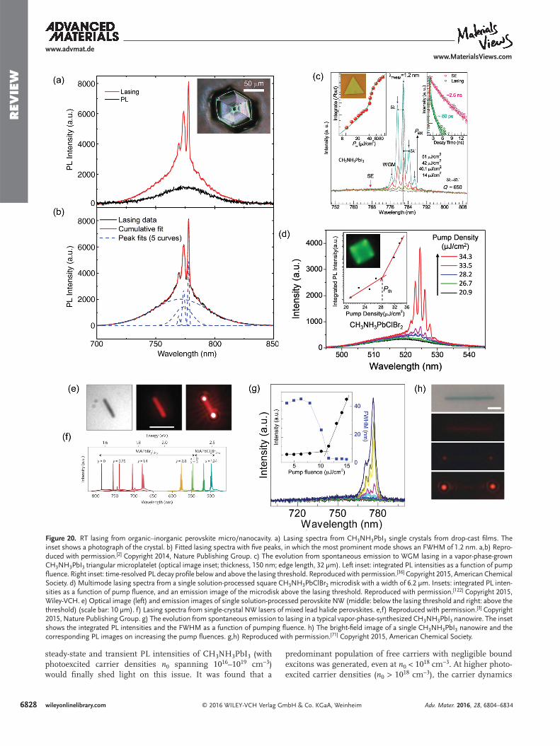
6828 wileyonlinelibrary.com © 2016 WILEY-VCH Verlag GmbH & Co. KGaA, Weinheim
REV
IEW
Adv. Mater. 2016, 28, 6804–6834
www.advmat.dewww.MaterialsViews.com
steady-state and transient PL intensities of CH 3 NH 3 PbI 3 (with photoexcited carrier densities n 0 spanning 10 16 –10 19 cm −3 ) would fi nally shed light on this issue. It was found that a
predominant population of free carriers with negligible bound excitons was generated, even at n 0 < 10 18 cm −3 . At higher photo-excited carrier densities ( n 0 > 10 18 cm −3 ), the carrier dynamics
Figure 20. RT lasing from organic–inorganic perovskite micro/nanocavity. a) Lasing spectra from CH 3 NH 3 PbI 3 single crystals from drop-cast fi lms. The inset shows a photograph of the crystal. b) Fitted lasing spectra with fi ve peaks, in which the most prominent mode shows an FWHM of 1.2 nm. a,b) Repro-duced with permission. [ 2 ] Copyright 2014, Nature Publishing Group. c) The evolution from spontaneous emission to WGM lasing in a vapor-phase-grown CH 3 NH 3 PbI 3 triangular microplatelet (optical image inset; thickness, 150 nm; edge length, 32 µm). Left inset: integrated PL intensities as a function of pump fl uence. Right inset: time-resolved PL decay profi le below and above the lasing threshold. Reproduced with permission. [ 36 ] Copyright 2015, American Chemical Society. d) Multimode lasing spectra from a single solution-processed square CH 3 NH 3 PbClBr 2 microdisk with a width of 6.2 µm. Insets: integrated PL inten-sities as a function of pump fl uence, and an emission image of the microdisk above the lasing threshold. Reproduced with permission. [ 122 ] Copyright 2015, Wiley-VCH. e) Optical image (left) and emission images of single solution-processed perovskite NW (middle: below the lasing threshold and right: above the threshold) (scale bar: 10 µm). f) Lasing spectra from single-crystal NW lasers of mixed lead halide perovskites. e,f) Reproduced with permission. [ 3 ] Copyright 2015, Nature Publishing Group. g) The evolution from spontaneous emission to lasing in a typical vapor-phase-synthesized CH 3 NH 3 PbI 3 nanowire. The inset shows the integrated PL intensities and the FWHM as a function of pumping fl uence. h) The bright-fi eld image of a single CH 3 NH 3 PbI 3 nanowire and the corresponding PL images on increasing the pump fl uences. g,h) Reproduced with permission. [ 71 ] Copyright 2015, American Chemical Society.

6829wileyonlinelibrary.com© 2016 WILEY-VCH Verlag GmbH & Co. KGaA, Weinheim
REV
IEW
Adv. Mater. 2016, 28, 6804–6834
www.advmat.dewww.MaterialsViews.com
are forced into a competition between the nonlinear processes of the radiative bimolecular recombination of the free elec-trons and holes and the non-radiative Auger recombination. Although the bimolecular recombination rate is ≈3–4 orders lower than that predicted by the Langevin model, [ 115,131 ] with no other relaxation pathways available, two-particle radiative
bimolecular recombination would still be more favorable than three-particle Auger recombination. The latter only domi-nates at excitations >10 19 cm −3 . [ 119 ] Interestingly, the Auger rates detected (≈10 −28 cm 6 s −1 ) [ 115,119 ] are comparable to that of strongly confi ned semiconductor colloidal quantum dots. Band fi lling by the free-electron–hole plasma that manifests as the
Figure 21. ASE/lasing from colloidal all-inorganic perovskite NPs. a) ASE spectra tuning via compositional modulation. b) Evolution from sponta-neous to WGM lasing with increasing pump intensity in a CsPbBr 3 NPs fi lm coated microsphere resonator of 15 µm in diameter. a,b) Reproduced with permission. [ 129 ] Copyright 2015, Nature Publishing Group. c) Pump-intensity-dependent PL spectra from a capillary tube infi ltrated with CsPbBr 3 NPs, with inner diameter of ≈50 µm. The left inset shows the pump-fl uence-dependent integrated PL intensities. The right insets show optical images of the NPs-infi ltrated capillary tube below (upper image) and above (lower image) the lasing threshold (scale bar is 20 µm). d) Fitted PL spectrum with two emission bands at high pump fl uence. e) Spectrally integrated PL intensity of two fi tted emission bands as a function of excitation intensity. c–e) Reproduced with permission. [ 127 ] Copyright 2015, Wiley-VCH.

6830 wileyonlinelibrary.com © 2016 WILEY-VCH Verlag GmbH & Co. KGaA, Weinheim
REV
IEW
Adv. Mater. 2016, 28, 6804–6834
www.advmat.dewww.MaterialsViews.com
Burstein–Moss effect [ 111 ] increases the Coulombic screening of the photogenerated electron–hole pairs and decreases the exciton binding energies. The carrier accumulation at the band edge provides the necessary population inversion condition needed for attaining light amplifi cation. Hence, stimulated emission out-competes the multiparticle processes [ 2,119 ] at elec-tron–hole plasma densities of ≈1–3 × 10 18 cm −3 .
In contrast to the electron–hole plasma recombination mechanism in the optical gain of CH 3 NH 3 PbX 3 perovskites, the origin of stimulated emission in CsPbX 3 NPs can be clearly ascribed to the recombination of bi-excitons. These bi-excitons possesses a binding energy of ≈50 meV – derived based on the energy separation between the exciton and bi-exciton peak posi-tions (Figure 21 d,e). [ 127 ] The large bi-exciton binding energy was found to drive the thermally stable RT bi-excitonic lasing and also help reduce the linear absorption losses.
5. Outlook
Organic–inorganic hybrid perovskites have the potential to replicate the breakthrough performances in photovoltaics and transform the fi eld of light emission. Although the present device performances (quantifi ed by brightness and current effi ciency) still lag behind technologies such as OLEDs and QLEDs, the surge achieved in merely two years promises to emulate established technologies. The basis of this projection is the remarkable intrinsic properties that these hybrid perov-skites possess, as well as their facile structural and photophys-ical tunability.
Smooth interfaces between the perovskite emitter and the electron/hole transport layers (or electrodes) will be para-mount for good charge injection and avoidance of parasitic non-radiative recombination from surface defects (i.e., pin-holes). Likewise, the formation of metallic Pb has also been identifi ed as major contributor to non-radiative losses. [ 40 ] To promote effi cient and balanced current injection, tailoring the band alignment of the devices through proper selection of the ETL and HTL, surface dipolar modifi cation, and doping can be pursued. Additionally, introduction of a very thin fi lm of insu-lating high-bandgap materials (e.g., poly(methyl methacrylate) (PMMA)) between the electrode and emitter layers, may help to reduce the concentration of a specifi c charge carrier, and thus promote balanced charge injection. [ 132 ] The minimization of optical losses by, e.g., employing light-coupling techniques or refraction index matching between device layers can be fol-lowed, similar to the approaches employed in current lighting technologies. Chemical and morphological control during thin-fi lm fabrication is thus key to optimal light emission, and these have already been substantially improved with a number of pro-cesses [ 37 ] and solvent-engineering approaches. High-effi ciency perovskite-solar-cell modules (i.e., >12%) have been achieved via various solution-based processing techniques (e.g., printing, slot-die coating, etc.), and it seems only matter of time that effi -cient light-emitting devices will leverage on these advances for large-area applications. In fact, the fi rst fully printed LED has already been demonstrated, displaying the highest recorded brightness (≈21 000 cd m −2 ), albeit at a low EQE (>1%). [ 105 ] Despite the possibility of transferring fabrication techniques
between solar-cell modules, PeLEDs, and lasers, several restric-tive characteristics for light emission, such as very thin homo-geneous emitter layers (to promote radiative recombination), would require new processes/formulations to be developed for scalability. To date, the largest PeLED fabricated had an area of 4 cm 2 . [ 40 ]
On the other hand, nanostructured perovskites like col-loidal NPs have displayed remarkable luminescence properties with quantum yields approaching 100% and high color purity. Despite much higher quantum yields and exciton binding energies than are observed in fi lms, the few perovskite QD devices reported to date [ 106,133 ] have delivered lower effi ciencies and brightness than thin-fi lm-based devices. Capping ligands, although effective in controlling the crystallization kinetics and size of the NPs, may hinder the formation of smooth thin fi lms. Their unfavorable wettability restricts the formation of smooth, pinhole-free fi lms, and, often, fastidious purifi cation steps are required to remove excess ligands. In turn, this may result in nanostructure coalescence (due to destabilization), and subse-quent photoluminescence quenching due to grain growth. [ 134 ] Device effi ciencies can be seriously affected by poor electrical injection due to remnant surface ligands. Although other approaches involving the use of polymer matrices to embed the NPs have been proposed, the challenge remains to look into novel strategies to fully utilize the extraordinary properties of nanostructured perovskites in light-emitting devices. The amal-gamation of confi nement strategies offered by NPs and high charge injection offered by thin fi lms, have resulted in the most effi cient PeLED (CE of 42 cd A −1 , EQE ≈ 8.5%), [ 40 ] where radia-tive recombination was signifi cantly enhanced through confi ne-ment of charge carriers in small grains within a thin-fi lm archi-tecture. Further improvements in device performances would need to address essential questions regarding the intrinsic material properties, the basic physical processes occurring within the perovskite material and optoelectronic devices. For example, the dominant charge-transport mechanisms, [ 135 ] or differences in PL emission originating from nanocrystals [ 113,136 ] and thin fi lms [ 2,4 ] of the same perovskite emitter need to be rec-onciled. A deeper understanding of the working mechanisms will be crucial to identify the limiting factor, and thus key to improving the device performance.
Besides enhancements in device performance, addressing the stability and long-term reliability of the materials and devices is paramount. Despite promising results obtained for solar cells by employing carbon fi lms as protective layers (>2500 h of operation), [ 137 ] the use of opaque fi lms is not fea-sible for light-emitting devices. Accelerated reliability tests at high relative humidity levels (75–80%) and a wide range of temperatures (−30 to 70 °C) would allow the estimation of the device lifetime. Furthermore, appropriate device encapsu-lation strategies and control of the fabrication ambient (e.g., fabrication in dry rooms utilized for battery assembly) would be necessary. Complications also involve structural instability originating from self-heating effects at high current densities (during operation) or under constant illumination. Encour-aging results have been obtained to address the former: by applying squared voltage pulses, the heat was allowed to dissi-pate between the pulses, and no signifi cant device degradation was observed. [ 5 ]

6831wileyonlinelibrary.com© 2016 WILEY-VCH Verlag GmbH & Co. KGaA, Weinheim
REV
IEW
Adv. Mater. 2016, 28, 6804–6834
www.advmat.dewww.MaterialsViews.com
Along with stability, toxicity concerns drive the need for lead replacement, especially with the susceptibility of perovskites to degrade in presence of moisture, leading to the formation of (water soluble) Pb species. This may seriously challenge the prospects of hybrid-perovskite-based technologies, and although several Pb-free perovskite alternatives (e.g., replace-ment Pb with Sn or Bi) have displayed promising photolu-minescence properties, the oxidation of Sn 2+ to Sn 4+ (i.e., the formation of p-type defects), [ 138 ] or the low-conductivity of Bi perovskites, [ 139 ] have raised new challenges. The use of inor-ganic cations (Cs + ) instead of the small organic CH 3 NH 3 + cat-ions, has already demonstrated extended ambient, as well as thermal stability, while retaining the 3D perovskite structure. Also, lower-dimensional layered perovskites may be exploited due to their intrinsically higher structural stability compared to 3D perovskites. The larger structural freedom allows for func-tionalization with specifi cally tailored chemical moieties, and improved moisture stability may be achieved through the intro-duction of large hydrophobic molecules. Another challenging set of factors is the behavior of halide perovskites under elec-trical stress. Ionic migration under high electric fi elds has been noted for some 3D perovskites, [ 107 ] and may result in compositional changes and subsequent perovskite degradation under standard PeLED operation. Such ionic migration may be tackled by appropriate choice of injection layers (which can also act as ion blockers), or through operation under lower and pulsed electrical bias. [ 5 ]
All the challenges outlined for PeLEDs would be appli-cable to lasers with the additional requirements of managing up to two order of magnitude higher carrier densities and intricate optical cavity design. Although ultralow ASE thresh-olds (<10 µJ cm −2 ) have been demonstrated, optical pumping has been done through femtosecond laser pulses that pack a high amount of optical power. Demonstration of optical ampli-fi cation lasting 100 ns required temperatures of 220 K and below. [ 140 ] The next challenge to be tackled for perovskites as a viable gain media would be to achieve ASE and lasing with nanosecond laser pulses and continuous wave (CW) pumping at room temperatures. Such demonstrations would need new perovskite materials designed to withstand heating from longer optical pump pulses, with higher absorption cross-sections, and decreased energy densities. Engineering of high- Q optical cavi-ties and high-quality resonator cavities for loss compensation would also be essential to effect reduction in gain thresholds. Although optically pumped polariton lasing has been observed in ZnO, [ 141 ] GaAs, [ 142 ] and GaN [ 143 ] systems, perovskite polariton lasers remain largely unexplored despite some early work in the mid-2000s. [ 144,145 ] The quantum-confi ned systems offered by lower-dimensionality layered perovskites and nanostructures would be top candidates to be explored for polariton lasing since they would allow for gain build-up to occur at much lower carrier lasing thresholds and allow for potentially thresholdless lasing with highly optimized cavities.
Despite the success in achieving solution-processed opti-cally pumped color-tunable lasing with relatively low fl uence threshold, electrically driven lasing remains a signifi cant chal-lenge. Several obstacles must be overcome, such as the very high current densities necessary to reach the threshold carrier density for ASE. As a reference, the largest current densities
achievable in standard OLED confi gurations (≈200–300 A cm −2 ) are signifi cantly lower than the prerequisite values for optical gain (>5 kA cm −2 ), [ 119 ] and, thus, the challenge would be to design new perovskite materials where the carrier density threshold for lasing is accessible. Moreover, heating effects must be reduced for electric laser devices, as higher current-injection densities can potentially degrade both the organic charge-injection lasers as well as the gain media. Careful materials design or device fabrication could overcome these challenges, e.g., through the use of all-inorganic perovskite NPs or lower-dimensional layered perovskites. For the device fabrication, electrically driven lasers using the LET confi gura-tion (rather than the conventional OLED structure) may be one promising direction. [ 146 ] The underlying rationale is that the LET confi guration allows for increased injected current densi-ties. In addition, the LET confi guration allows facile manipula-tion; the light-emitting medium can be placed far away from the source and drain electrodes in an attempt to reduce the non-radiative losses near the metal electrodes. [ 147 ] Furthermore, resonator designs (e.g., LET architecture with a DFB reso-nator) and use of high-quality single-crystalline thin fi lms or nanostructures (e.g., NWs, NRs, NPs, etc.) would augment the device performance by lowering the optically pumped lasing threshold even further.
6. Conclusions
The remarkable intrinsic properties and high degree of struc-tural fl exibility allow the potential for hybrid perovskites to go beyond academic curiosity and garner industrial interest. In particular the high quantum yields, narrow emission, high exciton binding energies, color tunability, and facile solution-processing at low temperatures should be exploited. Beyond applications as emitters and optical-gain materials, organic–inorganic hybrid perovskites may also be incorporated in cur-rently existing technologies as a replacement for phosphors. Identifi cation of Pb-free light emitters would be a critical area of focus; and the leverage provided by nanostructuring and by layered perovskites to control the binding energy and quantum yields holds the promise that the pursuit of Pb-free perov skite light emitters may be less challenging than that in photovoltaics. Emitter materials would need to be matched with selective contact materials, and the diversity of hetero-junctions, architectures, and processing conditions is certain to increase rapidly. En route toward commercialization, the opto-electronic properties (e.g., excitation dynamics, non-radiative recombination, etc.), the working principles, and degradation mechanisms of hybrid perovskite materials in light-emitting devices would need better understanding. The delicate inter-play between the localized physics occurring within the various organic/inorganic building blocks, along with the emergence of the delocalized behavior arising from such units embedded in a crystalline matrix, would need to be pursued. Buoyed by the successes in photovoltaics, it is reasonable to assume that research in perovskite optoelectronics will intensify in the foreseeable future ensuring a luminous future for organic–inorganic hybrid perovskites for applications in lasers and light-emitting devices.

6832 wileyonlinelibrary.com © 2016 WILEY-VCH Verlag GmbH & Co. KGaA, Weinheim
REV
IEW
Adv. Mater. 2016, 28, 6804–6834
www.advmat.dewww.MaterialsViews.com
Acknowledgements The authors acknowledge funding from the National Research Foundation Singapore (NRF) Program #: NRF-CRP14-2014-03 and through the Singapore–Berkeley Research Initiative for Sustainable Energy (SinBeRISE) CREATE Program. T.C.S. acknowledges the support from NTU start-up grant M4080514; the Ministry of Education AcRF Tier 1 grant RG101/15, and Tier 2 grants MOE2013-T2-1-081 and MOE2014-T2-1-044. N.M. would like to acknowledge the funding support from NTU-A*STAR Silicon Technologies Centre of Excellence under the program grant No. 11235100003 and MOE Tier 1 grant RG184/14. Finally, the authors thank Koh Teck Ming, Ng Yan Fong, I. V. Kameshwar Rao, and Fadilah Nur Bte Jamuludin for their help in preparing the fi gures.
Received: February 2, 2016 Revised: March 10, 2016
Published online: May 23, 2016
[1] NREL, 2016 , http://www.nrel.gov/ncpv/images/effi ciency_chart.jpg , accessed: April 2016 .
[2] G. Xing , N. Mathews , S. S. Lim , N. Yantara , X. Liu , D. Sabba , M. Grätzel , S. Mhaisalkar , T. C. Sum , Nat. Mater. 2014 , 13 , 476 .
[3] H. Zhu , Y. Fu , F. Meng , X. Wu , Z. Gong , Q. Ding , M. V. Gustafsson , M. T. Trinh , S. Jin , X. Y. Zhu , Nat. Mater. 2015 , 14 , 636 .
[4] O. A. Jaramillo-Quintero , R. S. Sanchez , M. Rincon , I. Mora-Sero , J. Phys. Chem. Lett. 2015 , 6 , 1883 .
[5] Z. K. Tan , R. S. Moghaddam , M. L. Lai , P. Docampo , R. Higler , F. Deschler , M. Price , A. Sadhanala , L. M. Pazos , D. Credgington , F. Hanusch , T. Bein , H. J. Snaith , R. H. Friend , Nat. Nanotechnol. 2014 , 9 , 687 .
[6] X. Y. Chin , D. Cortecchia , J. Yin , A. Bruno , C. Soci , Nat. Commun. 2015 , 6 , 7383 .
[7] C. Murawski , K. Leo , M. C. Gather , Adv. Mater. 2013 , 25 , 6801 . [8] Y. Shirasaki , G. J. Supran , M. G. Bawendi , V. Bulovic , Nat. Pho-
tonics 2013 , 7 , 13 . [9] S. D. Stranks , G. E. Eperon , G. Grancini , C. Menelaou ,
M. J. P. Alcocer , T. Leijtens , L. M. Herz , A. Petrozza , H. J. Snaith , Science 2013 , 342 , 341 .
[10] G. Xing , N. Mathews , S. Sun , S. S. Lim , Y. M. Lam , M. Grat··zel , S. Mhaisalkar , T. C. Sum , Science 2013 , 342 , 344 .
[11] S. De Wolf , J. Holovsky , S. J. Moon , P. Löper , B. Niesen , M. Ledinsky , F. J. Haug , J. H. Yum , C. Ballif , J. Phys. Chem. Lett. 2014 , 5 , 1035 .
[12] P. Santhanam , D. Huang , R. J. Ram , M. A. Remennyi , B. A. Matveev , Appl. Phys. Lett. 2013 , 103 , 183513 .
[13] Z. Hongping , L. Guangyu , Z. Jing , R. A. Arif , N. Tansu , J. Disp. Technol. 2013 , 9 , 212 .
[14] M. Shukla , N. Brahme , R. S. Kher , M. S. K. Khokhar , Indian J. Pure Appl. Phys. 2011 , 49 , 142 .
[15] L. Protesescu , S. Yakunin , M. I. Bodnarchuk , F. Krieg , R. Caputo , C. H. Hendon , R. X. Yang , A. Walsh , M. V. Kovalenko , Nano Lett. 2015 , 15 , 3692 .
[16] J. A. Sichert , Y. Tong , N. Mutz , M. Vollmer , S. Fischer , K. Z. Milowska , R. García Cortadella , B. Nickel , C. Cardenas-Daw , J. K. Stolarczyk , A. S. Urban , J. Feldmann , Nano Lett. 2015 , 15 , 6521 .
[17] D. H. Cao , C. C. Stoumpos , O. K. Farha , J. T. Hupp , M. G. Kanatzidis , J. Am. Chem. Soc. 2015 , 137 , 7843 .
[18] E. R. Dohner , E. T. Hoke , H. I. Karunadasa , J. Am. Chem. Soc. 2014 , 136 , 1718 .
[19] E. R. Dohner , A. Jaffe , L. R. Bradshaw , H. I. Karunadasa , J. Am. Chem. Soc. 2014 , 136 , 13154 .
[20] M. Kulbak , D. Cahen , G. Hodes , J. Phys. Chem. Lett. 2015 , 6 , 2452 .
[21] V. M. Goldschmidt , Naturwissenschaften 1926 , 14 , 477 . [22] C. Li , X. Lu , W. Ding , L. Feng , Y. Gao , Z. Guo , Acta Crystallogr.,
Sect. B: Struct. Sci. 2008 , 64 , 702 . [23] M. A. Green , A. Ho-Baillie , H. J. Snaith , Nat. Photonics 2014 , 8 ,
506 . [24] D. B. Mitzi , J. Chem. Soc., Dalton Trans. 2001 , 1 . [25] G. Kieslich , S. Sun , A. K. Cheetham , Chem. Sci. 2014 , 5 , 4712 . [26] M. Era , S. Morimoto , T. Tsutsui , S. Saito , Appl. Phys. Lett. 1994 , 65 ,
676 . [27] X. Hong , T. Ishihara , A. V. Nurmikko , Solid State Commun. 1992 ,
84 , 657 . [28] T. Hattori , T. Taira , M. Era , T. Tsutsui , S. Saito , Chem. Phys. Lett.
1996 , 254 , 103 . [29] T. Kondo , T. Azuma , T. Yuasa , R. Ito , Solid State Commun. 1998 ,
105 , 253 . [30] K. Chondroudis , D. B. Mitzi , Chem. Mater. 1999 , 11 , 3028 . [31] F. Deschler , M. Price , S. Pathak , L. E. Klintberg , D. D. Jarausch ,
R. Higler , S. Hüttner , T. Leijtens , S. D. Stranks , H. J. Snaith , M. Atatüre , R. T. Phillips , R. H. Friend , J. Phys. Chem. Lett. 2014 , 5 , 1421 .
[32] N. Yantara , S. Bhaumik , F. Yan , D. Sabba , H. A. Dewi , N. Mathews , P. P. Boix , H. V. Demir , S. Mhaisalkar , J. Phys. Chem. Lett. 2015 , 6 , 4360 .
[33] Y. Hassan , Y. Song , R. D. Pensack , A. I. Abdelrahman , Y. Kobayashi , M. A. Winnik , G. D. Scholes , Adv. Mater. 2015 , 28 , 566 .
[34] L. C. Schmidt , A. Pertegás , S. González-Carrero , O. Malinkiewicz , S. Agouram , G. Mínguez Espallargas , H. J. Bolink , R. E. Galian , J. Pérez-Prieto , J. Am. Chem. Soc. 2014 , 136 , 850 .
[35] D. Zhang , S. W. Eaton , Y. Yu , L. Dou , P. Yang , J. Am. Chem. Soc. 2015 , 137 , 9230 .
[36] Q. Zhang , S. T. Ha , X. Liu , T. C. Sum , Q. Xiong , Nano Lett. 2014 , 14 , 5995 .
[37] J. Burschka , N. Pellet , S.-J. Moon , R. Humphry-Baker , P. Gao , M. K. Nazeeruddin , M. Gratzel , Nature 2013 , 499 , 316 .
[38] G. Li , Z. K. Tan , D. Di , M. L. Lai , L. Jiang , J. H. W. Lim , R. H. Friend , N. C. Greenham , Nano Lett. 2015 , 15 , 2640 .
[39] J. Li , S. G. R. Bade , X. Shan , Z. Yu , Adv. Mater. 2015 , 27 , 5196 . [40] H. Cho , S.-H. Jeong , M.-H. Park , Y.-H. Kim , C. Wolf , C.-L. Lee ,
J. H. Heo , A. Sadhanala , N. Myoung , S. Yoo , S. H. Im , R. H. Friend , T.-W. Lee , Science 2015 , 350 , 1222 .
[41] Y. C. Kim , N. J. Jeon , J. H. Noh , W. S. Yang , J. Seo , J. S. Yun , A. Ho-Baillie , S. Huang , M. A. Green , J. Seidel , T. K. Ahn , S. I. Seok , Adv. Energy Mater. 2015 , 6 , 1502104 ; DOI: 10.1002/aenm.201502104 .
[42] G. E. Eperon , S. D. Stranks , C. Menelaou , M. B. Johnston , L. M. Herz , H. J. Snaith , Energy Environ. Sci. 2014 , 7 , 982 .
[43] C. C. Stoumpos , C. D. Malliakas , M. G. Kanatzidis , Inorg. Chem. 2013 , 52 , 9019 .
[44] D. P. McMeekin , G. Sadoughi , W. Rehman , G. E. Eperon , M. Saliba , M. T. Hörantner , A. Haghighirad , N. Sakai , L. Korte , B. Rech , M. B. Johnston , L. M. Herz , H. J. Snaith , Science 2016 , 351 , 151 .
[45] C. C. Stoumpos , C. D. Malliakas , J. A. Peters , Z. Liu , M. Sebastian , J. Im , T. C. Chasapis , A. C. Wibowo , D. Y. Chung , A. J. Freeman , B. W. Wessels , M. G. Kanatzidis , Cryst. Growth Des. 2013 , 13 , 2722 .
[46] S. Kondo , K. Takahashi , T. Nakanish , T. Saito , H. Asada , H. Nakagawa , Curr. Appl. Phys. 2007 , 7 , 1 .
[47] Z. Cheng , J. Lin , CrystEngComm 2010 , 12 , 2646 . [48] L. Dou , A. B. Wong , Y. Yu , M. Lai , N. Kornienko , S. W. Eaton ,
A. Fu , C. G. Bischak , J. Ma , T. Ding , N. S. Ginsberg , L.-W. Wang , A. P. Alivisatos , P. Yang , Science 2015 , 349 , 1518 .
[49] K. Gauthron , J. S. Lauret , L. Doyennette , G. Lanty , A. Al Choueiry , S. J. Zhang , A. Brehier , L. Largeau , O. Mauguin , J. Bloch , E. Deleporte , Opt. Express 2010 , 18 , 5912 .
6833wileyonlinelibrary.com© 2016 WILEY-VCH Verlag GmbH & Co. KGaA, Weinheim
REV
IEW
Adv. Mater. 2016, 28, 6804–6834
www.advmat.dewww.MaterialsViews.com
[50] A. Yangui , D. Garrot , J. S. Lauret , A. Lusson , G. Bouchez , E. Deleporte , S. Pillet , E. E. Bendeif , M. Castro , S. Triki , Y. Abid , K. Boukheddaden , J. Phys. Chem. C 2015 , 119 , 23638 .
[51] I. C. Smith , E. T. Hoke , D. Solis-Ibarra , M. D. McGehee , H. I. Karunadasa , Angew. Chem. 2014 , 126 , 11414 .
[52] D. B. Mitzi , K. Chondroudis , C. R. Kagan , Inorg. Chem. 1999 , 38 , 6246 .
[53] C. Motta , F. El-Mellouhi , S. Kais , N. Tabet , F. Alharbi , S. Sanvito , Nat. Commun. 2015 , 6 , 7026 .
[54] T. Ishihara , J. Takahashi , T. Goto , Phys. Rev. B 1990 , 42 , 11099 . [55] N. Kitazawa , M. Aono , Y. Watanabe , J. Phys. Chem. Solids 2011 , 72 ,
1467 . [56] G. C. Papavassiliou , I. B. Koutselas , Synth. Met. 1995 , 71 , 1713 . [57] P. Tyagi , S. M. Arveson , W. A. Tisdale , J. Phys. Chem. Lett. 2015 ,
6 , 1911 . [58] D. B. Mitzi , C. A. Feild , W. T. A. Harrison , A. M. Guloy , Nature
1994 , 369 , 467 . [59] J. Calabrese , N. L. Jones , R. L. Harlow , N. Herron , D. L. Thorn ,
Y. Wang , J. Am. Chem. Soc. 1991 , 113 , 2328 . [60] X. Wu , M. T. Trinh , D. Niesner , H. Zhu , Z. Norman , J. S. Owen ,
O. Yaffe , B. J. Kudisch , X. Y. Zhu , J. Am. Chem. Soc. 2015 , 137 , 2089 .
[61] T. M. Koh , V. Shanmugam , J. Schlipf , L. M.-B. Oesinghaus , P. R. Narayanan , V. Swamy , N. Mathews , P. P. Boix , S. G. Mhaisalkar , Adv. Mater. 2016 , DOI: 10.1002/adma.201506141 .
[62] S. Zhang , G. Lanty , J.-S. Lauret , E. Deleporte , P. Audebert , L. Galmiche , Acta Mater. 2009 , 57 , 3301 .
[63] S. Zhang , P. Audebert , Y. Wei , J.-S. Lauret , L. Galmiche , E. Deleporte , J. Mater. Chem. 2011 , 21 , 466 .
[64] P. Audebert , G. Clavier , V. Alain-Rizzo , E. Deleporte , S. Zhang , J.-S. Lauret , G. Lanty , C. Boissière , Chem. Mater. 2009 , 21 , 210 .
[65] M. Era , K. Maeda , T. Tsutsui , Chem. Lett. 1997 , 26 , 1235 . [66] M. I. Saidaminov , A. L. Abdelhady , B. Murali , E. Alarousu ,
V. M. Burlakov , W. Peng , I. Dursun , L. Wang , Y. He , G. MacUlan , A. Goriely , T. Wu , O. F. Mohammed , O. M. Bakr , Nat. Commun. 2015 , 6 , 7586 .
[67] S. Gonzalez-Carrero , R. E. Galian , J. Perez-Prieto , J. Mater. Chem. A 2015 , 3 , 9187 .
[68] H. Huang , A. S. Susha , S. V. Kershaw , T. F. Hung , A. L. Rogach , Adv. Sci. 2015 , 2 , 1500194 .
[69] F. Zhang , H. Zhong , C. Chen , X. G. Wu , X. Hu , H. Huang , J. Han , B. Zou , Y. Dong , ACS Nano 2015 , 9 , 4533 .
[70] A. B. Wong , M. Lai , S. W. Eaton , Y. Yu , E. Lin , L. Dou , A. Fu , P. Yang , Nano Lett. 2015 , 15 , 5519 .
[71] J. Xing , X. F. Liu , Q. Zhang , S. T. Ha , Y. W. Yuan , C. Shen , T. C. Sum , Q. Xiong , Nano Lett. 2015 , 15 , 4571 .
[72] X. Peng , L. Manna , W. Yang , J. Wickham , E. Scher , A. Kadavanich , A. P. Alivisatos , Nature 2000 , 404 , 59 .
[73] S. Pathak , N. Sakai , F. Wisnivesky Rocca Rivarola , S. D. Stranks , J. Liu , G. E. Eperon , C. Ducati , K. Wojciechowski , J. T. Griffi ths , A. A. Haghighirad , A. Pellaroque , R. H. Friend , H. J. Snaith , Chem. Mater. 2015 , 27 , 8066 .
[74] A. Sadhanala , S. Ahmad , B. Zhao , N. Giesbrecht , P. M. Pearce , F. Deschler , R. L. Z. Hoye , K. C. Gödel , T. Bein , P. Docampo , S. E. Dutton , M. F. L. De Volder , R. H. Friend , Nano Lett. 2015 , 15 , 6095 .
[75] Q. A. Akkerman , V. D’Innocenzo , S. Accornero , A. Scarpellini , A. Petrozza , M. Prato , L. Manna , J. Am. Chem. Soc. 2015 , 137 , 10276 .
[76] G. Nedelcu , L. Protesescu , S. Yakunin , M. I. Bodnarchuk , M. J. Grotevent , M. V. Kovalenko , Nano Lett. 2015 , 15 , 5635 .
[77] A. Swarnkar , R. Chulliyil , V. K. Ravi , M. Irfanullah , A. Chowdhury , A. Nag , Angew. Chem., Int. Ed. 2015 , 54 , 15424 .
[78] Y. Yin , A. P. Alivisatos , Nature 2005 , 437 , 664 .
[79] B. Luo , Y.-C. Pu , Y. Yang , S. A. Lindley , G. Abdelmageed , H. Ashry , Y. Li , X. Li , J. Z. Zhang , J. Phys. Chem. C 2015 , 119 , 26672 .
[80] N. Pradhan , D. Reifsnyder , R. Xie , J. Aldana , X. Peng , J. Am. Chem. Soc. 2007 , 129 , 9500 .
[81] M. Zhang , H. Yu , M. Lyu , Q. Wang , J. H. Yun , L. Wang , Chem. Commun. 2014 , 50 , 11727 .
[82] O. Vybornyi , S. Yakunin , M. V. Kovalenko , Nanoscale 2016 , 8 , 6278 . [83] D. N. Dirin , S. Dreyfuss , M. I. Bodnarchuk , G. Nedelcu ,
P. Papagiorgis , G. Itskos , M. V. Kovalenko , J. Am. Chem. Soc. 2014 , 136 , 6550 .
[84] Z. Ning , X. Gong , R. Comin , G. Walters , F. Fan , O. Voznyy , E. Yassitepe , A. Buin , S. Hoogland , E. H. Sargent , Nature 2015 , 523 , 324 .
[85] R. S. Sanchez , M. S. de la Fuente , I. Suarez , G. Muñoz-Matutano , J. P. Martinez-Pastor , I. Mora-Sero , Sci. Adv. 2016 , 2 , e1501104 .
[86] K. Wu , G. Liang , Q. Shang , Y. Ren , D. Kong , T. Lian , J. Am. Chem. Soc. 2015 , 137 , 12792 .
[87] Y. Ling , Z. Yuan , Y. Tian , X. Wang , J. C. Wang , Y. Xin , K. Hanson , B. Ma , H. Gao , Adv. Mater. 2015 , 28 , 305 .
[88] J. Even , L. Pedesseau , C. Katan , ChemPhysChem 2014 , 15 , 3733 . [89] Y. Bekenstein , B. A. Koscher , S. W. Eaton , P. Yang , A. P. Alivisatos ,
J. Am. Chem. Soc. 2015 , 137 , 16008 . [90] Z. Yuan , Y. Shu , Y. Tian , Y. Xin , B. Ma , Chem. Commun. 2015 , 51 ,
16385 . [91] H. Deng , D. Dong , K. Qiao , L. Bu , B. Li , D. Yang , H. E. Wang ,
Y. Cheng , Z. Zhao , J. Tang , H. Song , Nanoscale 2015 , 7 , 4163 . [92] N. Kitazawa , Y. Watanabe , Y. Nakamura , J. Mater. Sci. 2002 , 37 ,
3585 . [93] D. M. Jang , K. Park , D. H. Kim , J. Park , F. Shojaei , H. S. Kang ,
J.-P. Ahn , J. W. Lee , J. K. Song , Nano Lett. 2015 , 15 , 5191 . [94] N. Pellet , J. Teuscher , J. Maier , M. Grätzel , Chem. Mater. 2015 , 27 ,
2181 . [95] Z. Yuan , Y. Shu , Y. Xin , B. Ma , Chem. Commun. 2016 , 52 , 3887 . [96] J. B. Rivest , S. L. Swisher , L.-K. Fong , H. Zheng , A. P. Alivisatos ,
ACS Nano 2011 , 5 , 3811 . [97] D. H. Son , S. M. Hughes , Y. Yin , A. Paul Alivisatos , Science 2004 ,
306 , 1009 . [98] L. Gil-Escrig , G. Longo , A. Pertegás , C. Roldán-Carmona ,
A. Soriano , M. Sessolo , H. J. Bolink , Chem. Commun. 2015 , 51 , 569 .
[99] J. C. Yu , D. B. Kim , G. Baek , B. R. Lee , E. D. Jung , S. Lee , J. H. Chu , D. K. Lee , K. J. Choi , S. Cho , M. H. Song , Adv. Mater. 2015 , 27 , 3492 .
[100] J. Wang , N. Wang , Y. Jin , J. Si , Z. K. Tan , H. Du , L. Cheng , X. Dai , S. Bai , H. He , Z. Ye , M. L. Lai , R. H. Friend , W. Huang , Adv. Mater. 2015 , 27 , 2311 .
[101] R. L. Z. Hoye , M. R. Chua , K. P. Musselman , G. Li , M. L. Lai , Z. K. Tan , N. C. Greenham , J. L. MacManus-Driscoll , R. H. Friend , D. Credgington , Adv. Mater. 2015 , 27 , 1414 .
[102] Y. H. Kim , H. Cho , J. H. Heo , T. S. Kim , N. Myoung , C. L. Lee , S. H. Im , T. W. Lee , Adv. Mater. 2015 , 27 , 1248 .
[103] X. Zhang , H. Lin , H. Huang , C. Reckmeier , Y. Zhang , W. C. H. Choy , A. L. Rogach , Nano Lett. 2016 , 16 , 1415 .
[104] M. H. Song , J. C. Yu , D. B. Kim , E. D. Jung , B. R. Lee , Nanoscale 2016 , 8 , 7036 .
[105] S. G. R. Bade , J. Li , X. Shan , Y. Ling , Y. Tian , T. Dilbeck , T. Besara , T. Geske , H. Gao , B. Ma , K. Hanson , T. Siegrist , C. Xu , Z. Yu , ACS Nano 2015 , 10 , 1795 .
[106] H. Huang , F. Zhao , L. Liu , F. Zhang , X.-g. Wu , L. Shi , B. Zou , Q. Pei , H. Zhong , ACS Appl. Mater. Interfaces 2015 , 7 , 28128 .
[107] C. Eames , J. M. Frost , P. R. F. Barnes , B. C. O/’Regan , A. Walsh , M. S. Islam , Nat. Commun. 2015 , 6 , 7497 .
[108] T. Y. Yang , G. Gregori , N. Pellet , M. Grätzel , J. Maier , Angew. Chem., Int. Ed. 2015 , 54 , 7905 .

6834 wileyonlinelibrary.com © 2016 WILEY-VCH Verlag GmbH & Co. KGaA, Weinheim
REV
IEW
Adv. Mater. 2016, 28, 6804–6834
www.advmat.dewww.MaterialsViews.com
[109] H. Zhang , H. Lin , C. Liang , H. Liu , J. Liang , Y. Zhao , W. Zhang , M. Sun , W. Xiao , H. Li , S. Polizzi , D. Li , F. Zhang , Z. He , W. C. H. Choy , Adv. Funct. Mater. 2015 , 25 , 7226 .
[110] V. D’Innocenzo , G. Grancini , M. J. P. Alcocer , A. R. S. Kandada , S. D. Stranks , M. M. Lee , G. Lanzani , H. J. Snaith , A. Petrozza , Nat. Commun. 2014 , 5 , 3586 .
[111] J. S. Manser , P. V. Kamat , Nat. Photonics 2014 , 8 , 737 . [112] Q. Dong , Y. Fang , Y. Shao , P. Mulligan , J. Qiu , L. Cao , J. Huang ,
Science 2015 , 347 , 967 . [113] D. Shi , V. Adinolfi , R. Comin , M. Yuan , E. Alarousu , A. Buin ,
Y. Chen , S. Hoogland , A. Rothenberger , K. Katsiev , Y. Losovyj , X. Zhang , P. A. Dowben , O. F. Mohammed , E. H. Sargent , O. M. Bakr , Science 2015 , 347 , 519 .
[114] S. D. Stranks , H. J. Snaith , Nat. Nanotechnol. 2015 , 10 , 391 . [115] C. Wehrenfennig , G. E. Eperon , M. B. Johnston , H. J. Snaith ,
L. M. Herz , Adv. Mater. 2014 , 26 , 1584 . [116] J. M. Azpiroz , E. Mosconi , J. Bisquert , F. De Angelis , Energy
Environ. Sci. 2015 , 8 , 2118 . [117] M. Lenes , G. Garcia-Belmonte , D. Tordera , A. Pertegás , J. Bisquert ,
H. J. Bolink , Adv. Funct. Mater. 2011 , 21 , 1581 . [118] M. F. Aygüler , M. D. Weber , B. M. D. Puscher , D. D. Medina ,
P. Docampo , R. D. Costa , J. Phys. Chem. C 2015 , 119 , 12047 . [119] M. Saba , M. Cadelano , D. Marongiu , F. Chen , V. Sarritzu ,
N. Sestu , C. Figus , M. Aresti , R. Piras , A. Geddo Lehmann , C. Cannas , A. Musinu , F. Quochi , A. Mura , G. Bongiovanni , Nat. Commun. 2014 , 5 , 5049 .
[120] S. D. Stranks , S. M. Wood , K. Wojciechowski , F. Deschler , M. Saliba , H. Khandelwal , J. B. Patel , S. J. Elston , L. M. Herz , M. B. Johnston , A. P. H. J. Schenning , M. G. Debije , M. K. Riede , S. M. Morris , H. J. Snaith , Nano Lett 2015 , 15 , 4935 .
[121] M. Saliba , S. M. Wood , J. B. Patel , P. K. Nayak , J. Huang , J. A. Alexander-Webber , B. Wenger , S. D. Stranks , M. T. Hörantner , J. T.-W. Wang , R. J. Nicholas , L. M. Herz , M. B. Johnston , S. M. Morris , H. J. Snaith , M. K. Riede , Adv. Mater. 2015 , 28 , 923 .
[122] Q. Liao , K. Hu , H. H. Zhang , X. D. Wang , J. N. Yao , H. B. Fu , Adv Mater 2015 , 27 , 3405 .
[123] M. H. Huang , S. Mao , H. Feick , H. Q. Yan , Y. Y. Wu , H. Kind , E. Weber , R. Russo , P. D. Yang , Science 2001 , 292 , 1897 .
[124] H. M. Zhu , Y. P. Fu , F. Meng , X. X. Wu , Z. Z. Gong , Q. Ding , M. V. Gustafsson , M. T. Trinh , S. Jin , X. Y. Zhu , Nat Mater 2015 , 14 , 636 .
[125] V. I. Klimov , S. A. Ivanov , J. Nanda , M. Achermann , I. Bezel , J. A. McGuire , A. Piryatinski , Nature 2007 , 447 , 441 .
[126] V. I. Klimov , A. A. Mikhailovsky , S. Xu , A. Malko , J. A. Hollingsworth , C. A. Leatherdale , H. J. Eisler , M. G. Bawendi , Science 2000 , 290 , 314 .
[127] Y. Wang , X. Li , J. Song , L. Xiao , H. Zeng , H. Sun , Adv. Mater. 2015 , 27 , 7101 .
[128] J. Pan , S. P. Sarmah , B. Murali , I. Dursun , W. Peng , M. R. Parida , J. Liu , L. Sinatra , N. Alyami , C. Zhao , E. Alarousu , T. K. Ng , B. S. Ooi , O. M. Bakr , O. F. Mohammed , J. Phys. Chem. Lett. 2015 , 6 , 5027 .
[129] S. Yakunin , L. Protesescu , F. Krieg , M. I. Bodnarchuk , G. Nedelcu , M. Humer , G. De Luca , M. Fiebig , W. Heiss , M. V. Kovalenko , Nat. Commun. 2015 , 6 , 8056 .
[130] T. C. Sum , S. Chen , G. Xing , X. Liu , B. Wu , Nanotechnology 2015 , 26 , 342001 .
[131] T. J. Savenije , C. S. Ponseca , L. Kunneman , M. Abdellah , K. B. Zheng , Y. X. Tian , Q. S. Zhu , S. E. Canton , I. G. Scheblykin , T. Pullerits , A. Yartsev , V. Sundstrom , J. Phys. Chem. Lett. 2014 , 5 , 2189 .
[132] X. Dai , Z. Zhang , Y. Jin , Y. Niu , H. Cao , X. Liang , L. Chen , J. Wang , X. Peng , Nature 2014 , 515 , 96 .
[133] J. Song , J. Li , X. Li , L. Xu , Y. Dong , H. Zeng , Adv. Mater. 2015 , 27 , 7162 .
[134] Y. Kim , E. Yassitepe , O. Voznyy , R. Comin , G. Walters , X. Gong , P. Kanjanaboos , A. F. Nogueira , E. H. Sargent , ACS Appl. Mater. Interfaces 2015 , 7 , 25007 .
[135] T. M. Brenner , D. A. Egger , A. M. Rappe , L. Kronik , G. Hodes , D. Cahen , J. Phys. Chem. Lett. 2015 , 6 , 4754 .
[136] W. Nie , H. Tsai , R. Asadpour , J.-C. Blancon , A. J. Neukirch , G. Gupta , J. J. Crochet , M. Chhowalla , S. Tretiak , M. A. Alam , H.-L. Wang , A. D. Mohite , Science 2015 , 347 , 522 .
[137] H. Zhou , Y. Shi , Q. Dong , H. Zhang , Y. Xing , K. Wang , Y. Du , T. Ma , J. Phys. Chem. Lett. 2014 , 5 , 3241 .
[138] M. H. Kumar , S. Dharani , W. L. Leong , P. P. Boix , R. R. Prabhakar , T. Baikie , C. Shi , H. Ding , R. Ramesh , M. Asta , M. Graetzel , S. G. Mhaisalkar , N. Mathews , Adv. Mater. 2014 , 26 , 7122 .
[139] B.-W. Park , B. Philippe , X. Zhang , H. Rensmo , G. Boschloo , E. M. J. Johansson , Adv. Mater. 2015 , 27 , 6806 .
[140] M. Cadelano , V. Sarritzu , N. Sestu , D. Marongiu , F. Chen , R. Piras , R. Corpino , C. M. Carbonaro , F. Quochi , M. Saba , A. Mura , G. Bongiovanni , Adv. Opt. Mater. 2015 , 3 , 1557 .
[141] M. Li , G. Xing , G. Xing , B. Wu , T. Wu , X. Zhang , T. C. Sum , Phys. Rev. B 2013 , 87 , 115309 .
[142] M. Panahandeh-Fard , J. Yin , M. Kurniawan , Z. Wang , G. Leung , T. C. Sum , C. Soci , J. Phys. Chem. Lett. 2014 , 5 , 1144 .
[143] G. Christmann , R. Butté , E. Feltin , J.-F. Carlin , N. Grandjean , Appl. Phys. Lett. 2008 , 93 , 051102 .
[144] G. Lanty , J. S. Lauret , E. Deleporte , S. Bouchoule , X. Lafosse , Appl. Phys. Lett. 2008 , 93 , 081101 .
[145] G. Lanty , S. Zhang , J. S. Lauret , E. Deleporte , P. Audebert , S. Bouchoule , X. Lafosse , J. Zuñiga-Pérez , F. Semond , D. Lagarde , F. Médard , J. Leymarie , Phys. Rev. B 2011 , 84 , 195449 .
[146] E. B. Namdas , M. Tong , P. Ledochowitsch , S. R. Mednick , J. D. Yuen , D. Moses , A. J. Heeger , Adv. Mater. 2009 , 21 , 799 .
[147] T. Takenobu , S. Z. Bisri , T. Takahashi , M. Yahiro , C. Adachi , Y. Iwasa , Phys Rev Lett 2008 , 100 , 066601 .
[148] R. Meerheim , M. Furno , S. Hofmann , B. Lüssem , K. Leo , Appl. Phys. Lett. 2010 , 97 , 253305 .
[149] N. K. Kumawat , A. Dey , K. L. Narasimhan , D. Kabra , ACS Photonics 2015 , 2 , 349 .
[150] B. R. Sutherland , S. Hoogland , M. M. Adachi , C. T. O. Wong , E. H. Sargent , ACS Nano 2014 , 8 , 10947 .
[151] R. Dhanker , A. N. Brigeman , A. V. Larsen , R. J. Stewart , J. B. Asbury , N. C. Giebink , Appl Phys Lett 2014 , 105 , 151112 .
[152] S. W. Eaton , M. Lai , N. A. Gibson , A. B. Wong , L. Dou , J. Ma , L.-W. Wang , S. R. Leone , P. Yang , Proc. Natl. Acad. Sci. USA 2016 , 113 , 1993 .

本文献由“学霸图书馆-文献云下载”收集自网络,仅供学习交流使用。
学霸图书馆(www.xuebalib.com)是一个“整合众多图书馆数据库资源,
提供一站式文献检索和下载服务”的24 小时在线不限IP
图书馆。
图书馆致力于便利、促进学习与科研,提供最强文献下载服务。
图书馆导航:
图书馆首页 文献云下载 图书馆入口 外文数据库大全 疑难文献辅助工具