Performance of a High Voltage Power Supply … of a High Voltage Power Supply Incorporating a...
5
Performance of a High Voltage Power Supply Incorporating a Ceramic Transformer Yoshiaki Shikaze, Masatosi Imori , Hideyuki Fuke, Hiroshi Matsumoto and Takashi Taniguchi Department of Physics, Faculty of Science, University of Tokyo 7-3-1 Hongo, Bunkyo-ku, Tokyo 113-0033, Japan International Center for Elementary Particle Physics, University of Tokyo High Energy Accelerator Research Organization (KEK) 1-1 Oho, Tsukuba-shi, Ibaraki-ken 305-0801, Japan Abstract This paper describes the performance of a high voltage power supply incorporating a ceramic transformer. Since the transformer doesn’t include any magnetic material the power supply can be operated under a strong magnetic field. In the article, the efficiency of the power supply is studied against various parameters. It was found that the efficiency reaches more than 50 percent when zero-voltage switching was realized. From a 3V supply voltage, the power supply can produce 3000V at a 21 megohm load. A 5V supply voltage is enough to supply 4000V at the same load. The high voltage power supply is tested in a magnetic field of 1.5 tesla. The performance of the power supply seems almost intact in the magnetic field. I. INTRODUCTION This paper describes the performance of a power supply incorporating a ceramic transformer which uses the piezoelectric effect to generate high voltage. By using the ceramic transformer and an air-core coil, the power supply can produce high voltage under a strong magnetic field. The high voltage power supply described in the article is intended to produce high voltage efficiently under a strong magnetic field [1]. The output high voltage is stabilized by feedback. A feedback loop includes divider resistors, an error amplifier, a voltage controlled oscillator (VCO) and a driver circuit. An output high voltage is produced by a Cockcroft-Walton (CW) circuit. The driver circuit generates a sinusoidal carrier the frequency of which is generated by the VCO. The driver circuit drives the transformer, applying the sinusoidal carrier. The amplitude ratio of the transformer has dependence on the frequency, which is utilized by the feedback. The transformer shows a sharp resonance in the vicinity of 120kHz. From a viewpoint of efficiency, it is favorable to drive the transformer at efficient frequencies ranging from 120kHz to 124kHz. The driver circuit includes MOS FETs and the air-core coils. The inductance of the coil and the input capacitance of the transformer composes a oscillation circuit, by which the sinusoidal carrier is produced. The inductance is adjusted so that the frequency of the oscillation can be in the efficient range. So the FETs are switched while the voltage applied to the FETs is zero. The zero-voltage switching(ZVS) of the FET was realized, which contributed to improving the efficiency. II. CIRCUIT DESCRIPTION The circuit of the high voltage supply is shown in Fig. 1. The high voltage supply is composed of the ceramic transformer, a cockcroft walton circuit, divider resistors, an error amplifier, a VCO and a driver circuit. The output of the error amplifier is supplied to the VCO. Then the VCO produces a carrier wave which is frequency-modulated by the output of the error amplifier. The modulation satisfies the condition that the frequency of the carrier wave stays higher than the resonance frequency of the ceramic transformer. The carrier wave drives the ceramic transformer through the driver circuit. Since voltage amplitude at the output of the ceramic transformer depends on the frequency of the carrier wave, the ceramic transformer converts frequency modulation at the input to amplitude modulation at the output. The carrier wave modulated in amplitude is demodulated by rectification, and the output of the ceramic transformer is demodulated by the CW circuit. So the output from the CW circuit is the delayed and distorted output of the error amplifier. The output high voltage, which is the output of the CW circuit, is divided by the divider resistors and then fed back to the error amplifier. The resonance shown by the ceramic transformer is sharp, and then voltage amplification of the transformer, increasing rapidly in the vicinity of the resonance frequency, depends largely on the frequency of the carrier wave. The output high voltage is stabilized by feedback, where the frequency dependence is utilized. The output high voltage is fed back to the error amplifier to be compared with a reference voltage. The voltage difference between the input of the error amplifier is amplified and fed to the VCO, which then adjusts the frequency of the carrier wave so as to reduce the voltage difference.
Transcript of Performance of a High Voltage Power Supply … of a High Voltage Power Supply Incorporating a...

Performance of a High Voltage Power SupplyIncorporating a Ceramic Transformer
Yoshiaki Shikaze, Masatosi Imori1, Hideyuki Fuke, Hiroshi Matsumoto1 and Takashi Taniguchi2
Department of Physics, Faculty of Science, University of Tokyo7-3-1 Hongo, Bunkyo-ku, Tokyo 113-0033, Japan
1International Center for Elementary Particle Physics, University of Tokyo2High Energy Accelerator Research Organization (KEK)
1-1 Oho, Tsukuba-shi, Ibaraki-ken 305-0801, Japan
Abstract
This paper describes the performance of a high voltagepower supply incorporating a ceramic transformer. Sincethe transformer doesn’t include any magnetic material thepower supply can be operated under a strong magneticfield. In the article, the efficiency of the power supply isstudied against various parameters. It was found that theefficiency reaches more than 50 percent when zero-voltageswitching was realized. From a 3V supply voltage, thepower supply can produce 3000V at a 21 megohm load.A 5V supply voltage is enough to supply 4000V at thesame load. The high voltage power supply is tested in amagnetic field of 1.5 tesla. The performance of the powersupply seems almost intact in the magnetic field.
I. INTRODUCTION
This paper describes the performance of a powersupply incorporating a ceramic transformer which uses thepiezoelectric effect to generate high voltage. By using theceramic transformer and an air-core coil, the power supplycan produce high voltage under a strong magnetic field.The high voltage power supply described in the article isintended to produce high voltage efficiently under a strongmagnetic field [1].
The output high voltage is stabilized by feedback. Afeedback loop includes divider resistors, an error amplifier,a voltage controlled oscillator (VCO) and a driver circuit.An output high voltage is produced by a Cockcroft-Walton(CW) circuit. The driver circuit generates a sinusoidalcarrier the frequency of which is generated by the VCO.The driver circuit drives the transformer, applying thesinusoidal carrier. The amplitude ratio of the transformerhas dependence on the frequency, which is utilized by thefeedback.
The transformer shows a sharp resonance in the vicinityof 120kHz. From a viewpoint of efficiency, it is favorableto drive the transformer at efficient frequencies rangingfrom 120kHz to 124kHz. The driver circuit includes MOSFETs and the air-core coils. The inductance of the coiland the input capacitance of the transformer composesa oscillation circuit, by which the sinusoidal carrier is
produced. The inductance is adjusted so that the frequencyof the oscillation can be in the efficient range. So the FETsare switched while the voltage applied to the FETs is zero.The zero-voltage switching(ZVS) of the FET was realized,which contributed to improving the efficiency.
II. CIRCUIT DESCRIPTION
The circuit of the high voltage supply is shown inFig. 1. The high voltage supply is composed of theceramic transformer, a cockcroft walton circuit, dividerresistors, an error amplifier, a VCO and a driver circuit.
The output of the error amplifier is supplied to theVCO. Then the VCO produces a carrier wave which isfrequency-modulated by the output of the error amplifier.The modulation satisfies the condition that the frequencyof the carrier wave stays higher than the resonancefrequency of the ceramic transformer.
The carrier wave drives the ceramic transformerthrough the driver circuit. Since voltage amplitude atthe output of the ceramic transformer depends on thefrequency of the carrier wave, the ceramic transformerconverts frequency modulation at the input to amplitudemodulation at the output.
The carrier wave modulated in amplitude isdemodulated by rectification, and the output of the ceramictransformer is demodulated by the CW circuit. So theoutput from the CW circuit is the delayed and distortedoutput of the error amplifier. The output high voltage,which is the output of the CW circuit, is divided by thedivider resistors and then fed back to the error amplifier.
The resonance shown by the ceramic transformer issharp, and then voltage amplification of the transformer,increasing rapidly in the vicinity of the resonancefrequency, depends largely on the frequency of the carrierwave. The output high voltage is stabilized by feedback,where the frequency dependence is utilized. The outputhigh voltage is fed back to the error amplifier to becompared with a reference voltage. The voltage differencebetween the input of the error amplifier is amplified andfed to the VCO, which then adjusts the frequency of thecarrier wave so as to reduce the voltage difference.

3K1.5K
10K
OPA 234 P INA122 P
TPS 2813 P
100 M Ω
200
OPA 234 P
KΩ
Ceramic
Transformer
2 SK2796L
9 V
Reference Voltage
µ H
9 V
Output
TC4027 BP
JK
CLKQ
Q
µ PD5555
12
3V~5V 0V
50K
LM385 -2.5
3V 3V Return LM385-1.2
x2
x2
x 6 ESJA98 x 6
Ω
KΩ Ω
ΩΩ
Ω
Ω
5K Ω
Driver Circuit
Voltage-Controlled Oscillator
Error Amplifier
100nF
100nF
100nF
1KΩ
50
48K29
0.1nF
180pF
100K
Ω47
Ω47
22 Ω
22 Ω
-
Fig. 1 Schematic circuit of the high voltage power supply, where an error amplifier is implemented by INA122 and OPA234 and avoltage controlled oscillator by PD5555 and TC4027.
which eliminates the power consumed by a dampedcapacitance mainly due to the ceramic transformer. Thedriver circuit includes two identical resonant circuits asshown in Fig. 1, each of which is composed of a MOSFET and a inductor(implemented by an air-core coil). TheFETs are simultaneously switched on and off alternatelyby the output of the VCO. The inductance in the resonantcircuit resonates with the damped capacitance of theceramic transformer while the FET is turned off, and theinductor stores the current while the FET is turned on.One resonant circuit makes a half sinusoidal wave whoseamplitude is about 3 times of the voltage supplied to theresonant circuit. The other resonant circuit makes theother half sinusoidal wave alternatively. Thus the resonantcircuit generates a quasi-sinusoidal carrier wave at theinput terminals of the ceramic transformer. The FETs areswitched over while the voltage applied between the inputterminals stays almost zero volt.
III. PERFORMANCE OF HIGH VOLTAGE
POWER SUPPLY WITH CERAMIC
TRANSFORMER
The high voltage supply is implemented on a printedboard as shown in Fig 2.
Fig. 2 A picture of the high voltage power supply described in thearticle.
A. Inductance Dependence on Efficiency
In order to improve the efficiency, it is important torealize the ZVS at the driver circuit. So the range of thefrequency where the ZVS is realized is studied in therelation with the inductance of the two air-core coils in thedriver circuit. The ZVS is realized at lower frequenciesthan the frequency of the resonance at the driver circuit.The frequency of the resonance at the driver circuit largelydepends on the inductance. The performance of the powersupply is measured at inductances of 40H, 50H, 65H,80H and 100H. Efficiency is analyzed form a viewpointof the ZVS and its dependence on the frequency of the

VCO.In Fig. 3 and 4, the output high voltage versus the VCO
frequency, the efficiency versus the VCO frequency, andthe efficiency versus the output high voltage are plottedfor each inductance, where the efficiency is a ratio of thepower consumption by a 21 megohm load to the powersupplied to the driver circuit. The efficiency increases asthe frequency come close to the resonance frequency ofabout 120kHz and reaches the almost constant value ofmore than 50 %.
Fig. 5 and 6 show the output voltage of each singleFET. Fig. 7 and 8 show the quasi-sinusoidal wavewhich are the voltage difference between the output oftwo FETs. The quasi-sinusoidal wave is applied to thetransformer. Where the efficiency is more than 50 %, thequasi-sinusoidal wave is nearly a ideal sinusoidal waveand ZVS is realized as shown in Fig. 6 and 8.
When the frequency is not in the efficient range, theefficiency is low and the ZVS isn’ t realized as shown inFig. 5 and 7. The voltage range of efficient high voltagegeneration is dependent of the inductance. As for theefficiency versus output high voltage, it can be seen thatthe plateau of efficiency is wider for a smaller inductance,and that a larger inductance reaches a higher plateauin efficiency. So it seems important not to select suchthe inductance that locates the frequency of resonanceat the driver circuit close to the resonance frequency ofthe transformer. Placing the frequency of resonance atthe driver circuit in the efficient range of the frequencycontributes to improving the efficiency of the powersupply.
Fig. 3 Dependence of the output high voltage and of the efficiencyon the VCO frequency are shown for each inductance : the supplyvoltage to the driver circuit is 3V and 2SK2796L is employed.
B. Dependence of MOS-FET on Efficiency
The MOS-FET used in the driver circuit is alsoimportant for efficiency. Low power MOS-FETs
Fig. 4 Dependence of the efficiency on the output high voltage isshown for each inductance.
Fig. 5 900V, 130.1kHz Fig. 6 2550V, 121.2kHz
Fig. 7 900V, 130.1kHz Fig. 8 2550V, 121.2kHz
with various on-resistance were selected and tested.Specifications of the selected MOS-FETs are summarizedin the Table 1. In Fig. 9 (a), the efficiency versus outputhigh voltage are shown for selected MOS-FETs. InFig. 9 (b), maximum output high voltage versus the supplyvoltage to the driver circuit are plotted.
Drain-Source input Turn-onon-Resi.(ohm) C.(pF) Delay-time(ns)
2SK1151 3.5 160 52SK2796L 0.12 180 92SK2933 0.040 500 102SK2939 0.020 1100 15
Table 1Typical specifications of the MOS-FETs
MOS-FET 2SK1151 with an on-resistance of 3.5ohm is worse in both the maximum output high voltageand the efficiency than others with lower on-resistance.The on-resistance of the MOS-FET should be low forefficiency. Yet the capacitance in the MOS-FET with

lower on-resistance tends to be larger. A large inputcapacitance of the MOS-FET may causes considerablepower consumption. The large capacitance leads to longdelays which are unsuitable for the ZVS. Therefore, weselected 2SK2796L to be used in the power supply.
Supply voltage to driver circuit
Max
. out
put H
V
Output HV
Eff
icie
ncy
Fig. 9 (a): Efficiency vs. output high voltage plot for each FET.;(b): Plot of maximum output high voltage for each FET.
C. Supply Voltage Effect on Efficiency and onmaximum Output Voltage
The supply voltage to the driver circuit is raised tothe output high voltage. The high voltage power supplygenerates the high voltage power supply efficiently froma low supply voltage. Efficiency is investigated froma viewpoint of the dependence on the supply voltage.Fig. 10 and 11 provide the plots of the efficiency versusthe output high voltage for each supply voltage, where2SK2796L is employed in the driver circuit. As seenfrom Fig. 10, a 2V supply voltage can produce the outputhigh voltage close to 2800V with high efficiency. FromFig. 9(b), a 1.6V supply voltage can generate the outputhigh voltage close to 2400V.
The amplitude of the sinusoidal carrier is about threetimes the supply voltage to the driver circuit. The outputvoltage of the transformer is furthermore multiplied byabout six times in the CW circuit. When the supplyvoltage to the driver circuit is 2V, the maximum outputhigh voltage reaches 2700V at a load of 21 megohm. Itcan be seen that the amplitude ratio of the transformerreaches more than eighty around the resonance. Thismeans a 5V supply voltage to the driver circuit is largeenough to produce a 4000V output high voltage.
D. Dependence of Capacitance in CW Circuit
Capacitors with several values were tested in CWcircuit, and its effect on efficiency was studied. Capacitorsof 220F, 100F, 33F and 12F were employed for test.
Fig. 10 Output high voltage and efficiency are plotted for eachsupply voltage against VCO frequency.
Fig. 11 Efficiency vs. output high voltage plot for each supplyvoltage.
We checked the noise level and the efficiency for eachcapacitor, plotting the efficiency versus the output highvoltage as shown in Fig. 12. It can be seen that efficiencydoes not depend on the capacitance. A capacitor of smallercapacitance will works in the CW circuit.
E. Static and Dynamic Stability
Static and dynamic responses of the power supplywere measured. Fig. 13 shows the setup of the responsemeasurement. A mercuric switch was employed toimplement instant change of load in magnitude such aschanging from 21 megohm to zero megohm and from zeromegohm to 21 megohm. The change of the load causes atransient response at the output high voltage.
Stability of the power supply were estimated bymeasuring transient responses at the output high voltage.The transient responses at the output high voltage areshown in Fig. 14. The power supply described in thearticle shows quick feedback. The static response at the
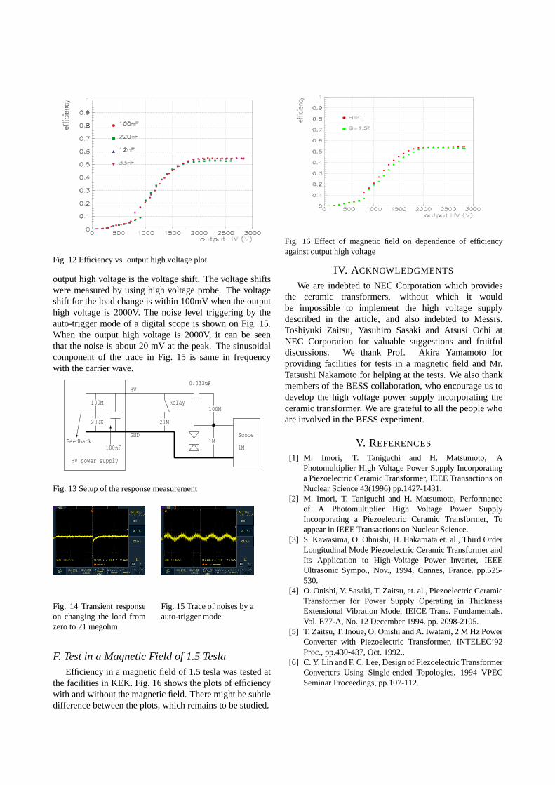
Fig. 12 Efficiency vs. output high voltage plot
output high voltage is the voltage shift. The voltage shiftswere measured by using high voltage probe. The voltageshift for the load change is within 100mV when the outputhigh voltage is 2000V. The noise level triggering by theauto-trigger mode of a digital scope is shown on Fig. 15.When the output high voltage is 2000V, it can be seenthat the noise is about 20 mV at the peak. The sinusoidalcomponent of the trace in Fig. 15 is same in frequencywith the carrier wave.
100M
200K
Feedback100nF
21M
Relay
1M
100M
0.033uFHV
GND
1M
Scope
HV power supply
Fig. 13 Setup of the response measurement
Fig. 14 Transient responseon changing the load fromzero to 21 megohm.
Fig. 15 Trace of noises by aauto-trigger mode
F. Test in a Magnetic Field of 1.5 TeslaEfficiency in a magnetic field of 1.5 tesla was tested at
the facilities in KEK. Fig. 16 shows the plots of efficiencywith and without the magnetic field. There might be subtledifference between the plots, which remains to be studied.
Fig. 16 Effect of magnetic field on dependence of efficiencyagainst output high voltage
IV. ACKNOWLEDGMENTS
We are indebted to NEC Corporation which providesthe ceramic transformers, without which it wouldbe impossible to implement the high voltage supplydescribed in the article, and also indebted to Messrs.Toshiyuki Zaitsu, Yasuhiro Sasaki and Atsusi Ochi atNEC Corporation for valuable suggestions and fruitfuldiscussions. We thank Prof. Akira Yamamoto forproviding facilities for tests in a magnetic field and Mr.Tatsushi Nakamoto for helping at the tests. We also thankmembers of the BESS collaboration, who encourage us todevelop the high voltage power supply incorporating theceramic transformer. We are grateful to all the people whoare involved in the BESS experiment.
V. REFERENCES
[1] M. Imori, T. Taniguchi and H. Matsumoto, APhotomultiplier High Voltage Power Supply Incorporatinga Piezoelectric Ceramic Transformer, IEEE Transactions onNuclear Science 43(1996) pp.1427-1431.
[2] M. Imori, T. Taniguchi and H. Matsumoto, Performanceof A Photomultiplier High Voltage Power SupplyIncorporating a Piezoelectric Ceramic Transformer, Toappear in IEEE Transactions on Nuclear Science.
[3] S. Kawasima, O. Ohnishi, H. Hakamata et. al., Third OrderLongitudinal Mode Piezoelectric Ceramic Transformer andIts Application to High-Voltage Power Inverter, IEEEUltrasonic Sympo., Nov., 1994, Cannes, France. pp.525-530.
[4] O. Onishi, Y. Sasaki, T. Zaitsu, et. al., Piezoelectric CeramicTransformer for Power Supply Operating in ThicknessExtensional Vibration Mode, IEICE Trans. Fundamentals.Vol. E77-A, No. 12 December 1994. pp. 2098-2105.
[5] T. Zaitsu, T. Inoue, O. Onishi and A. Iwatani, 2 M Hz PowerConverter with Piezoelectric Transformer, INTELEC’92Proc., pp.430-437, Oct. 1992..
[6] C. Y. Lin and F. C. Lee, Design of Piezoelectric TransformerConverters Using Single-ended Topologies, 1994 VPECSeminar Proceedings, pp.107-112.