PEB-2772VGATM R1.1.pdf
53
PEB-2772VGATM Embedded System Board User's Manual Version 1.1 Copyright © Portwell, Inc., 2012 All rights reserved. All other brand names are registered trademarks of their respective owners.
Transcript of PEB-2772VGATM R1.1.pdf

PEB-2772VGATM
Embedded System Board
User's Manual
Version 1.1
Copyright © Portwell, Inc., 2012 All rights reserved. All other brand names are registered trademarks of their respective owners.

Preface
Table of Contents How to Use This Manual
Chapter 1 System Overview.......................................................................................................1-1 1.1 Introduction ....................................................................................................... 1-1 1.2 Check List........................................................................................................... 1-1 1.3 Product Specification........................................................................................ 1-2 1.4 System Configuration....................................................................................... 1-3 1.5 System Architecture.......................................................................................... 1-5
Chapter 2 Hardware Configuration ...........................................................................................2-1 2.1 Jumper Setting ................................................................................................... 2-1 2.2 Connector Allocation........................................................................................ 2-3
Chapter 3 System Installation....................................................................................................3-1 3.1 Intel ® Atom TM Processor D2550 ................................................................. 3-1 3.2 Main Memory .................................................................................................... 3-1 3.3 Installing the Single Board Computer............................................................ 3-1
3.3.1 Chipset Component Driver .................................................................... 3-3 3.3.2 Intel Graphics Media accelerator ........................................................... 3-3 3.3.3 Intel Gigabit Ethernet Controller ........................................................... 3-3 3.3.4 Audio Controller ...................................................................................... 3-3
3.4 Clear CMOS Operation .................................................................................... 3-4 3.5 WDT Function ................................................................................................... 3-5 3.6 GPIO.................................................................................................................... 3-7
Chapter 4 BIOS Setup Information............................................................................................4-1 4.1 Entering Setup ................................................................................................... 4-1 4.2 Main .................................................................................................................... 4-2 4.3 Configuration .................................................................................................... 4-3 4.4 Security ............................................................................................................. 4-20 4.5 Boot ................................................................................................................... 4-21 4.6 Security ............................................................................................................. 4-22
Chapter 5 Troubleshooting ........................................................................................................5-1 5.1 Hardware Quick Installation........................................................................... 5-1 5.2 FAQ ..................................................................................................................... 5-2
Appendix A
Appendix B

Preface
How to Use This Manual
The manual describes how to configure your PEB-2772 system to meet various operating requirements. It is divided into five chapters, with each chapter addressing a basic concept and operation of Single Host Board. Chapter 1 : System Overview. Presents what you have in the box and give you an overview of the product specifications and basic system architecture for this series model of single host board. Chapter 2 : Hardware Configuration. Shows the definitions and locations of Jumpers and Connectors that you can easily configure your system. Chapter 3 : System Installation. Describes how to properly mount the CPU, main memory and Compact Flash to get a safe installation and provides a programming guide of Watch Dog Timer function. Chapter 4 : BIOS Setup Information. Specifies the meaning of each setup parameters, how to get advanced BIOS performance and update new BIOS. In addition, POST checkpoint list will give users some guidelines of trouble-shooting. Chapter 5 : Troubleshooting. Provides various useful tips to quickly get PEB-2772 running with success. As basic hardware installation has been addressed in Chapter 3, this chapter will basically focus on system integration issues, in terms of backplane setup, BIOS setting, and OS diagnostics. The content of this manual is subject to change without prior notice. These changes will be incorporated in new editions of the document. Portwell may make supplement or change in the products described in this document at any time. Updates to this manual, technical clarification, and answers to frequently asked questions will be shown on the following web site : http://www.portwell.com.tw/.
System Overview
PEB-2772AVGATM User’s Manual 1-1
Chapter 1 System Overview
1.1 Introduction Portwell Inc., a world-leading innovator in the Industrial PC (IPC) market and a member of the Intel® Embedded and Communications Alliance (Intel ECA), announced today the Portwell PEB-2772 utilizing the Intel® ECX form factor based on the Intel® Atom™ processor D2550 and the Intel® System Controller Hub NM10, includes integrated, enhanced graphics and memory controllers on 32nm process technology, delivering significant power reduction, performance improvements and smaller platform footprint over the previous Intel® Atom™ processor D525. The PEB-2772 can provide the low power consumption for low profile fanless applications such as POS, Print Imaging, ATM, Kiosk, Medical, Panel PC, Digital Security and Digital Signage. PEB-2772 supports multi display by HDMI and VGA and 18/24-bit LVDS. With its display-enriched interface, PEB-2772 can support various multimedia devices and enriched IO interfaces that can supply various USB and COM devices. PEB-2772 supports SO-DIMM memory slot for DDR3 SDRAM up to 4GB, 4 x COM ports(1x Com port on rear IO/3x Com port on board header), 2 xSATA, 1 x Gigabit Ethernet, 6 x USB2.0 ports(1x USB port on rear IO/5x USB port on board header). It also support one Mini-PCIE socket for embedded application usage. 1.2 Check List The PEB-2772 package should cover the following basic items
One PEB-2772VGATM 3.5’ Main Board One Thermal Kit One Serial ATA cable One SATA Power Y-cable One Installation Resources CD-Title
If any of these items is damaged or missing, please contact your vendor and keep all packing materials for future replacement and maintenance.

System Overview
PEB-2772AVGATM User’s Manual 1-2
1.3 Product Specification
Main Processor - Intel® Atom™ D2550 dual-core processor - CPU clock speed: 1.86GHz
Chipset
Intel® NM10 chipset
System BIOS Phoenix BIOS
Main Memory One 204 - pin DDR3 SODIMM socket support up to 4GB 800/1066 MHz memory
Expansion Interface One PCIex1
SATA Interface Two SATA ports (SATA 3Gb)
Serial Port - Support three RS232 com port(1x Com port on rear IO/2x Com port on board
header) - Support one RS232/422/485 com port on board header
USB Interface Support Sex USB (Universal Serial Bus) ports, one on rear I/O and five on board header for internal devices
Audio Interface Connector for Line-Out(Line-out / Line-out / Mic-in pin header on board)
Real Time Clock/Calendar (RTC) Support Y2K Real Time Clock/Calendar
Watch Dog Timer - Support WDT function through software programming for enable/disable and
interval setting - General system reset
On-board Ethernet LAN One Gigabit Ethernet (10/100/1000 Mbits/sec) LAN ports
High Drive GPIO One pin-header for 8 bit GPIO (4bit in & 4bit out)

System Overview
PEB-2772AVGATM User’s Manual 1-3
System Monitoring Feature Monitor system temperature and major power sources.
Outline Dimension (L x W) 146mm (5.75”) X 105mm (4.0”)
Power Requirements Configuration
1.4 System Configuration
System Configuration CPU Type Intel (R) Atom(TM) CPU D2550 @1.86GHz FSB:533MHz SBC BIOS Portwell, Inc.PEB-2772VGATM BIOS Rev.:R1.00.W3(07092012) Memory Transcend DDR3 1066 SODIMM 2G(SEC HCH9K4B1G0846F) VGA Card Onboard Intel® Graphics Media Accelerator 3600 Series VGA Driver Intel® Graphics Media Accelerator 3600 Series Ver:8.14.8.1075 LAN Card Onboard Intel® 82583V Gigabit Network Connection LAN Driver Intel® 82583V Gigabit Network Connection Ver:11.11.43.0 Audio Card Onboard Realtek ALC886 High Defintion Audio Audio Driver Realtek High Defintion Audio Ver:6.0.1.6602 Chip Driver Intel® chipset Device software Ver:9.3.0.1019 SATA HDD Seagate ST3160318AS 160G CDROM ASUS DRW-24B35T Power Supply Seasonic SSA-0651-1 12V
Operating Temperature 0 °C ~ 60 °C
Storage temperature -20 ~ 80 °C
Relative Humidity 0% ~ 90%, non-condensing

System Overview
PEB-2772AVGATM User’s Manual 1-4
Mechanical Drawing

System Overview
PEB-2772AVGATM User’s Manual 1-5
1.5 System Architecture All of details operating relations are shown in PEB-2772VGATM System Block Diagram.
PEB-2772VGATM System Block Diagram

System Installation
PEB-2772AVGATM User’s Manual 2-1
Chapter 2 Hardware Configuration This chapter gives the definitions and shows the positions of jumpers, headers and connector. All of the configuration jumpers on PEB-2772VGTM are in the proper position. The default settings are indicated with a star sign (★). 2.1 Jumper Setting In general, jumpers on the single board computer are used to select options for certain features. Some of the jumpers are designed to be user-configurable, allowing for system enhancement. The others are for testing purpose only and should not be altered. To select any option, cover the jumper cap over (SHORT) or remove (NC) it from the jumper pins according to the following instructions. Here NC stands for “Not Connect”
Component side(Ver0.0)

System Installation
PEB-2772AVGATM User’s Manual 2-2
Solder side
System Installation
PEB-2772AVGATM User’s Manual 2-3
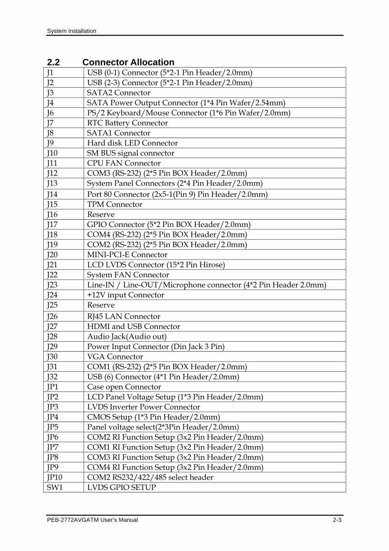
2.2 Connector Allocation J1 USB (0-1) Connector (5*2-1 Pin Header/2.0mm) J2 USB (2-3) Connector (5*2-1 Pin Header/2.0mm) J3 SATA2 Connector J4 SATA Power Output Connector (1*4 Pin Wafer/2.54mm) J6 PS/2 Keyboard/Mouse Connector (1*6 Pin Wafer/2.0mm) J7 RTC Battery Connector J8 SATA1 Connector J9 Hard disk LED Connector J10 SM BUS signal connector J11 CPU FAN Connector J12 COM3 (RS-232) (2*5 Pin BOX Header/2.0mm) J13 System Panel Connectors (2*4 Pin Header/2.0mm) J14 Port 80 Connector (2x5-1(Pin 9) Pin Header/2.0mm) J15 TPM Connector J16 Reserve J17 GPIO Connector (5*2 Pin BOX Header/2.0mm) J18 COM4 (RS-232) (2*5 Pin BOX Header/2.0mm) J19 COM2 (RS-232) (2*5 Pin BOX Header/2.0mm) J20 MINI-PCI-E Connector J21 LCD LVDS Connector (15*2 Pin Hirose) J22 System FAN Connector J23 Line-IN / Line-OUT/Microphone connector (4*2 Pin Header 2.0mm) J24 +12V input Connector J25 Reserve J26 RJ45 LAN Connector J27 HDMI and USB Connector J28 Audio Jack(Audio out) J29 Power Input Connector (Din Jack 3 Pin) J30 VGA Connector J31 COM1 (RS-232) (2*5 Pin BOX Header/2.0mm) J32 USB (6) Connector (4*1 Pin Header/2.0mm) JP1 Case open Connector JP2 LCD Panel Voltage Setup (1*3 Pin Header/2.0mm) JP3 LVDS Inverter Power Connector JP4 CMOS Setup (1*3 Pin Header/2.0mm) JP5 Panel voltage select(2*3Pin Header/2.0mm) JP6 COM2 RI Function Setup (3x2 Pin Header/2.0mm) JP7 COM1 RI Function Setup (3x2 Pin Header/2.0mm) JP8 COM3 RI Function Setup (3x2 Pin Header/2.0mm) JP9 COM4 RI Function Setup (3x2 Pin Header/2.0mm) JP10 COM2 RS232/422/485 select header SW1 LVDS GPIO SETUP
System Installation
PEB-2772AVGATM User’s Manual 2-4
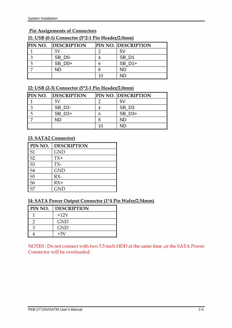
Pin Assignments of Connectors J1: USB (0-1) Connector (5*2-1 Pin Header/2.0mm) PIN NO. DESCRIPTION PIN NO. DESCRIPTION 1 5V 2 5V 3 SB_D0- 4 SB_D1 5 SB_D0+ 6 SB_D1+ 7 ND 8 ND 10 ND
J2: USB (2-3) Connector (5*2-1 Pin Header/2.0mm) PIN NO. DESCRIPTION PIN NO. DESCRIPTION 1 5V 2 5V 3 SB_D2- 4 SB_D3 5 SB_D2+ 6 SB_D3+ 7 ND 8 ND 10 ND
J3: SATA2 Connector) PIN NO. DESCRIPTION S1 GND S2 TX+ S3 TX- S4 GND S5 RX- S6 RX+ S7 GND
J4: SATA Power Output Connector (1*4 Pin Wafer/2.54mm) PIN NO. DESCRIPTION
1 +12V 2 GND 3 GND 4 +5V
NOTES : Do not connect with two 3.5-inch HDD at the same time ,or the SATA Power Connector will be overloaded.

System Installation
PEB-2772AVGATM User’s Manual 2-5
J6: PS/2 Keyboard/Mouse connector (1*6 Pin Wafer/2.0mm) PIN NO. DESCRIPTION
1 K/B CLK 2 M/S DATA 3 K/B DATE 4 KB5V 5 M/S CLK 6 GND
J9: Hard disk LED Connector PIN NO. DESCRIPTION 1 5V 2 Hard Disk signal
J10: SM BUS signal connector PIN NO. DESCRIPTION
1 SM_CLK 2 NC(No Key) 3 GND 4 SM_DATA 5 5V
J11: CPU FAN Connector PIN NO. DESCRIPTION
1 Fan Speed Detect 2 +12V 3 Fan Speed Driver
J12: COM3 (RS-232) (2*5 Pin BOX Header/2.0mm) PIN NO. DESCRIPTION PIN NO. DESCRIPTION
1 DCD#3 2 DSR#3 3 RXD#3 4 RTS#3 5 TXD#3 6 CTS#3 7 DTR#3 8 V_RI3 9 GND 10 NC

System Installation
PEB-2772AVGATM User’s Manual 2-6
J13: System Panel Connectors (2*4 Pin Header/2.0mm) PIN NO. DESCRIPTION PIN NO. DESCRIPTION
1 5VSB 2 SUSEND LED- 3 PWRLED+ 4 PWRLED- 5 GND 6 SYS_RESET# 7 PWR_ON_SW# 8 GND
J14: Port 80 Connector (2*5-1(Pin 9) Pin Header/2.0mm) PIN NO. DESCRIPTION PIN NO. DESCRIPTION 1 LPC AD0 2 +3.3V 3 LPC AD1 4 RESET 5 LPC AD2 6 LPC FRAME 7 LPC AD3 8 LPC PCICLK 10 NC
J15: TPM Connector PIN NO. DESCRIPTION PIN NO. DESCRIPTION
1 PCLK_TPM 2 GND 3 LFRAME# 4 NC 5 PLT_RST# 6 VCC 7 LAD3 8 LAD2 9 VCC3 10 LAD1 11 LAD0 12 GND 13 SMB_CLK 14 SMB_DATA 15 3V_DUAL 16 SERIRQ 17 GND 18 NC 19 LPCPD# 20 NC
J16: Reserve J17: GPIO Connector (5*2 Pin BOX Header/2.0mm) PIN NO. DESCRIPTION PIN NO. DESCRIPTION 1 GPIO50 2 GPIO54 3 GPIO51 4 GPIO55 5 GPIO52 6 GPIO56 7 GPIO53 8 GPIO57 9 +5V 10 GND

System Installation
PEB-2772AVGATM User’s Manual 2-7
J18: COM4 (RS-232) (2*5 Pin BOX Header/2.0mm) PIN NO. DESCRIPTION PIN NO. DESCRIPTION 1 DCD#4 2 DSR#4 3 RXD#4 4 RTS#4 5 TXD#4 6 CTS#4 7 DTR#4 8 V_RI4 9 GND 10 NC
J19: COM2 (RS-232) (2*5 Pin BOX Header/2.0mm) PIN NO. DESCRIPTION PIN NO. DESCRIPTION 1 DCD#2 2 DSR#2 3 RXD#2 4 RTS#2 5 TXD#2 6 CTS#2 7 DTR#2 8 V_RI2 9 GND 10 NC
J20: MINI-PCI-E Connector J21: LCD LVDS Connector (15*2 Pin Hirose) PIN NO. DESCRIPTION PIN NO. DESCRIPTION 2 VDD_LVDS 1 VDD_LVDS 4 NC 3 NC 6 NC 5 NC 8 NC 7 NC 10 NC 9 NC 12 NC 11 NC 14 NC 13 NC 16 Ground 15 Ground 18 LCD_DO0- 17 LCD_DO0+ 20 LCD_DO1- 19 LCD_DO1+ 22 LCD_DO2- 21 LCD_DO2+ 24 LCD_DO3- 23 LCD_DO3+ 26 LCD_CLK- 25 LCD_CLK+ 28 NC 27 NC 30 Ground 29 Ground
J22: System FAN Connector PIN NO. DESCRIPTION
1 Fan Speed Detect 2 +12V 3 Fan Speed Driver

System Installation
PEB-2772AVGATM User’s Manual 2-8
J23: Line-IN / Line-OUT/Microphone connector (4*2 Pin Header 2.0mm) PIN NO. DESCRIPTION PIN NO. DESCRIPTION 1 MIC_L 2 Line in L 3 GND 4 Line in R 5 Line out L 6 GND 7 Line out R 8 MIC_R
J24: +12V input Connector) PIN NO. Signal Description
1 GND 2 GND 3 +12V 4 +12V
J25: Reserve J26: RJ45 LAN Connector J27: HDMI and USB Connector) J28: Audio Jack(Audio out)
J29: Power Input Connector (Din Jack 3 Pin) PIN NO. DESCRIPTION
1 VIN 2 GND 3 GND CG1 GND
J30: VGA Connector J31: COM1 (RS-232) (2*5 Pin BOX Header/2.0mm) PIN NO. DESCRIPTION PIN NO. DESCRIPTION 1 DCD#2 2 DSR#2 3 RXD#2 4 RTS#2 5 TXD#2 6 CTS#2 7 DTR#2 8 V_RI2 9 GND 10 NC
System Installation
PEB-2772AVGATM User’s Manual 2-9
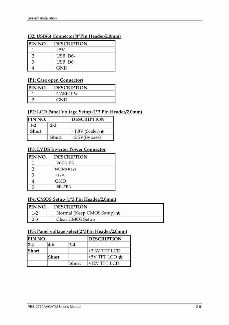
J32: USB(6) Connector(4*Pin Header/2.0mm) PIN NO. DESCRIPTION
1 +5V 2 USB_D6- 3 USB_D6+ 4 GND
JP1: Case open Connector) PIN NO. DESCRIPTION
1 CASEOP# 2 GND
JP2: LCD Panel Voltage Setup (1*3 Pin Header/2.0mm) PIN NO. DESCRIPTION 1-2 2-3 Short +1.8V (Scaler)★ Short +2.5V(Bypass)
JP3: LVDS Inverter Power Connector PIN NO. DESCRIPTION
1 VCC5_PS 2 NC(No Key) 3 +12V 4 GND 5 BKLTEN
JP4: CMOS Setup (1*3 Pin Header/2.0mm) PIN NO. DESCRIPTION
1-2 Normal (Keep CMOS Setup) ★ 2-3 Clear CMOS Setup
JP5: Panel voltage select(2*3Pin Header/2.0mm) PIN NO. DESCRIPTION 2-4 4-6 3-4 Short +3.3V TFT LCD Short +5V TFT LCD ★ Short +12V TFT LCD

System Installation
PEB-2772AVGATM User’s Manual 2-10
JP6/JP7/JP8/JP9:COM RI Function Setup (3*2 Pin Header/2.0mm)
PIN NO. DESCRIPTION 1-2 3-4 5-6
Short +5V Output Short RI Function ★ Short +12V Output
NOTES:COM1 (J31/JP7), COM2(J19/JP6), COM3(J12/JP8), COM4(J18/JP9) JP10: COM2 RS232/422/485 select header
PIN NO. DESCRIPTION 5-6 9-11 10-12 15-17 16-18 Other
Short Short Short Short Short Open RS-232 Function★PIN NO. DESCRIPTION
3-4 7-9 8-10 13-15 14-16 21-22 Other Short Short Short Short Short Short Open RS-422 Function
PIN NO. DESCRIPTION 1-2 7-9 8-10 19-20 Other
Short Short Short Short Open RS-485 Function SW1: LVDS GPIO SETUP Action GPIO Status
Short 0 Open 1
SW1 Pin Number Single Description
1、2 GPIO0 3、4 GPIO1 5、6 GPIO2 7、8 GPIO3
The default of GPIO:
GPIO3 GPIO2 GPIO1 GPIO0
0 1 1 0

System Installation
PEB-2772AVGATM User’s Manual 2-11

System Installation
PEB-2772AVGATM User’s Manual 3-1
Chapter 3 System Installation This chapter provides you with instructions to set up your system. The additional information is enclosed to help you set up onboard PCI device and handle Watch Dog Timer (WDT) and operation of GPIO in software programming. 3.1 Intel ® Atom TM Processor D2550 Passively-cooled, soldered-down Dual-Core Intel ® Atom™ processor D2550 with integrated graphics and integrated memory controller that’s suitable for fanless system and low-watt design. 3.2 Main Memory PEB-2772 provide 1 x 204-pin SO-DIMM sockets which supports 1066 DDR3-SDRAM as main memory, Non-ECC (Error Checking and Correcting), non-register functions. The maximum memory size can be up to 4GB capacity. Memory clock and related settings can be detected by BIOS via SPD interface. Watch out the contact and lock integrity of memory module with socket, it will impact on the system reliability. Follow normal procedures to install memory module into memory socket. Before locking, make sure that all modules have been fully inserted into the card slots. Note: DDR3 1333 MHz and DDR3 1600 MHz memory will run at 1066 MHz 3.3 Installing the Single Board Computer To install your PEB-2772 into standard chassis or proprietary environment, please perform the following: Step 1 : Check all jumpers setting on proper position Step 2 : Install memory module onto memory socket Step 3 : Place PEB-2772 into the dedicated position in the system Step 4 : Attach cables to existing peripheral devices and secure it WARNING Please ensure that SBC is properly inserted and fixed by mechanism. Note:

System Installation
PEB-2772AVGATM User’s Manual 3-2
Please refer to section 3.3.1 to 3.3.7 to install INF/VGA/LAN/Audio drivers.

System Installation
PEB-2772AVGATM User’s Manual 3-3
3.3.1 Chipset Component Driver The chipset on PEB-2772 is a new chipset that a few old operating systems might not be able to recognize. To overcome this compatibility issue, for Windows Operating Systems such as Windows 7, please install its INF driver before any other drivers installation. You can easily find the chipset component driver in PEB-2772 VGTAM CD-title. 3.3.2 Intel Graphics Media accelerator The Intel ® Atom TM Processor D2550 contains an integrated graphics core, the Intel ® GMA 3600 graphics controller, This combination makes PEB-2772 an excellent piece of multimedia hardware, PEB-2772 supports VGA, HDMI and also LVDS out put. The VGA port supports analog displays. The maximum supported resolution is 1920 x 1200 (WUXGA) at a 60 Hz refresh rate. VGA port enabled from POST whenever monitor is connected. For other Drivers Support Please find Intel® GMA 3600 driver in PEB-2772 CD-title. Driver supports Windows7 only. 3.3.3 Intel Gigabit Ethernet Controller Drivers Support Please find Intel 82583V Ethernet driver in /Ethernet directory of PEB-2772 CD-title. The drivers support Windows 7. LED Indicator (for LAN staturtS PEB-2772 provides two LED indicators to report Intel 82566MM Gigabit Ethernet interface status. Please refer to the table below as a quick reference guide.
Operation of Ethernet Port 82583V Color Name of LED
Linked Active Status LED Orange LAN Linked & Active LED On Blinking
Speed LED
Orange LAN speed LED Giga Mbps 100 Mbps 10 Mbps
3.3.4 Audio Controller Please find Realtek ALC886 Audio driver form PEB-2772 CD-title. The drivers support Windows 7.

System Installation
PEB-2772AVGATM User’s Manual 3-4
3.4 Clear CMOS Operation The following table indicates how to enable/disable Clear CMOS Function hardware circuit by putting jumpers at proper position. JP4:COMS Setup (1*3 Pin Header/2.0 mm
PIN No Description 1-2 Normal (Keep CMOS Setup)★ 2-3 Clear CMOS Setup

System Installation
PEB-2772AVGATM User’s Manual 3-5
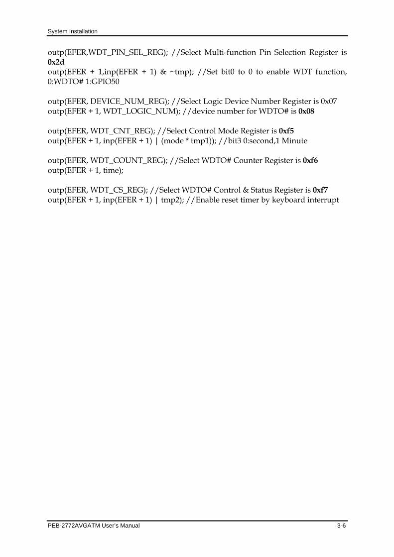
3.5 WDT Function The working algorithm of the WDT function can be simply described as a counting process. The Time-Out Interval can be set through software programming. The availability of the time-out interval settings by software or hardware varies from boards to boards. PEB-2772VGATM allows users control WDT through dynamic software programming. The WDT starts counting when it is activated. It sends out a signal to system reset or to non-maskable interrupt (NMI), when time-out interval ends. To prevent the time-out interval from running out, a re-trigger signal will need to be sent before the counting reaches its end. This action will restart the counting process. A well-written WDT program should keep the counting process running under normal condition. WDT should never generate a system reset or NMI signal unless the system runs into troubles. The related Control Registers of WDT are all included in the following sample program that is written in C language. User can fill a non-zero value into the Time-out Value Register to enable/refresh WDT. System will be reset after the Time-out Value to be counted down to zero. Or user can directly fill a zero value into Time-out Value Register to disable WDT immediately. To ensure a successful accessing to the content of desired Control Register, the sequence of following program codes should be step-by-step run again when each register is accessed. Additionally, there are maximum 2 seconds of counting tolerance that should be considered into user’ application program. For more information about WDT, please refer to Winbond W83627UHG data sheet. There are 7 PNP I/O port addresses that can be used to configure WDT, 1) 0x2E:EFER (Extended Function Enable Register, for identifying CR index number) 2) 0x07:DEVICE_NUM_REG (Logic Device Number Register) 3) 0x2d:WDT_PIN_SEL_REG (Multi-function Pin Selection Register for WDT ) 4) 0x08: WDT_LOGIC_NUM (Logic device number for WDT) 5) 0xf5:WDT_CNT_REG (WDT Control Mode Register. Using for setting time unit.) 6) 0xf6:WDT_COUNT_REG (WDTO# Counter Register. Using for setting the time.) 7) 0xf7:WDT_CS_REG (WDTO# Control & Status Register.) Below are some example codes, which demonstrate the use of WDT. //Enter the Extended Function Mode outp(EFER, 0x87); outp(EFER, 0x87); //Enable WDT function
System Installation
PEB-2772AVGATM User’s Manual 3-6
outp(EFER,WDT_PIN_SEL_REG); //Select Multi-function Pin Selection Register is 0x2d outp(EFER + 1,inp(EFER + 1) & ~tmp); //Set bit0 to 0 to enable WDT function, 0:WDTO# 1:GPIO50 outp(EFER, DEVICE_NUM_REG); //Select Logic Device Number Register is 0x07 outp(EFER + 1, WDT_LOGIC_NUM); //device number for WDTO# is 0x08 outp(EFER, WDT_CNT_REG); //Select Control Mode Register is 0xf5 outp(EFER + 1, inp(EFER + 1) | (mode * tmp1)); //bit3 0:second,1 Minute outp(EFER, WDT_COUNT_REG); //Select WDTO# Counter Register is 0xf6 outp(EFER + 1, time); outp(EFER, WDT_CS_REG); //Select WDTO# Control & Status Register is 0xf7 outp(EFER + 1, inp(EFER + 1) | tmp2); //Enable reset timer by keyboard interrupt

System Installation
PEB-2772AVGATM User’s Manual 3-7
3.6 GPIO #define EFER 0x2e //Address for Extended Function Enable Register #define DEVICE_NUM_REG 0x07 //Address for Logic Device Number Register #define GPIO_LOGIC_NUM 0x08 //Logic device number for GPIO #define GPIO_BASE_REG 0x30 //Set GPIO #define GPIO_IO_REG 0xe0 //Address for GPIO I/O Register #define GPIO_MODE_OUT 0 #define GPIO_DATA_REG 0xe1 //Address for GPIO Data Register int GPIO_Pin_Set(int pin_num, int mode, int value){ int tmp = 1 << pin_num; if(pin_num < 0 || pin_num > MAX_GPIO_NUM || mode < 0 || mode > 1 || value < 0 || value > 1){ printf("GPIO_Pin_Set:Invalid parameter\n"); return -1; } //Enter the Extended Function Mode outp(EFER, 0x87); outp(EFER, 0x87); //Now set the configuration register outp(EFER, DEVICE_NUM_REG); //Select Logic Device Number Register outp(EFER + 1, GPIO_LOGIC_NUM); //device number for GPIO2,3,4,5 is 9 outp(EFER, GPIO_BASE_REG); outp(EFER + 1, 0x07); outp(EFER, GPIO_IO_REG); //Select GPIO3 I/O Register outp(EFER + 1,(inp(EFER + 1) & ~tmp) | (tmp * mode));//Set I/O mode, 0:output 1:input //If mode is GPO, set value if(mode == GPIO_MODE_OUT){ outp(EFER, GPIO_DATA_REG); //Select GPIO3 Data Register outp(EFER + 1,(inp(EFER + 1) & ~tmp) | (tmp * value));//Set GPO value, 0:low 1:high printf("GPIO_Pin_Set: Set GPIO(%d) to GPO, Value = %d\n", pin_num, value); } else{ printf("GPIO_Pin_Set: Set GPIO(%d) to GPI\n", pin_num); } //Exit the Extended Function Mode

System Installation
PEB-2772AVGATM User’s Manual 3-8
o4utp(EFER, 0xAA); return 0; }

BIOS Setup Information
PEB-2772AVGATM User’s Manual 4-1
Chapter 4 BIOS Setup Information PEB-2772 equipped with the Phoenix BIOS stored in SPI Flash. BIOS has built-in setup program that allows users to adjust the basic system configuration. This type of information is stored in CMOS RAM that it is retained even if power-off periods. When system turns on, PEB-2772 communicates with peripheral devices and checks its hardware resources referring to the configuration information stored in CMOS memory. If any error occurs, or CMOS parameters need to be defined, the diagnostic program will prompt to user to enter the SETUP program. Some errors are significant that’ll abort the start-up process too. 4.1 Entering Setup Turn on or reboot the computer. When the message “Hit <F2> if you want to run SETUP” appears, press <F2> key immediately to enter BIOS setup program. If the message disappears before you respond, but you still wish to enter Setup, please restart the system to try “COLD START” again by turning it OFF and then ON, or touch the "RESET" button. You may also restart from “WARM START” by pressing <Ctrl>, <Alt>, and <Delete> keys simultaneously. If you do not press the keys at the right time and the system will not boot, an error message will be displayed and you will again be asked to, Press <F2> to Run SETUP or Resume In HIFLEX BIOS setup, you can use the keyboard to choose among options or modify the system parameters to match the options with your system. The table below will show you all of keystroke functions in BIOS setup.

BIOS Setup Information
PEB-2772AVGATM User’s Manual 4-2
4.2 Main Once you enter PEB-2772 Phoenix BIOS CMOS Setup Utility, a Main Menu is presented. The Main Menu allows user to select from eleven setup functions and two exit choices. Use arrow keys to switch among items and press <Enter> key to accept or bring up the sub-menu. This setup page includes all the items in standard compatible BIOS. Use the arrow keys to highlight the item and then use the <PgUp>/<PgDn> or <+>/<-> keys to select the value or number you want in each item and press <Enter> key to certify it. Follow command keys in CMOS Setup table to change Date, Time, Drive type and any other setup options.
System Time The time format is <Hour> <Minute> <Second>. Use [+] or [-] to configure system Time. System Date The date format is <Day>, <Month> <Date> <Year>. Use [+] or [-] to configure system Date.

BIOS Setup Information
PEB-2772AVGATM User’s Manual 4-3
4.3 Configuration This section allows users to configure further BIOS function.
Boot Configuration

BIOS Setup Information
PEB-2772AVGATM User’s Manual 4-4
Diagnostic Splash Screen This item shows a Diagnostic screen during boot up. This screen is also accessible through the App Menu.
The choice: Enabled, Disabled. Diagnostic Summary Screen This item shows a Diagnostic Summary Screen during boot up. The boot process will stop by displaying this screen until a key is pressed. The choice: Enabled, Disabled. UEFI Boot This item enables the UEFI Boot. Enable this function if you want to boot UEFI aware operation systems like Windows 7 64Bit or Linux.
The choice: Enabled, Disabled. Legacy Boot Enable the Legacy boot
Choices: Enabled, Disabled PCI/PCIE Configuration

BIOS Setup Information
PEB-2772AVGATM User’s Manual 4-5
ICH PCI Express Configuration
DMI Link ASPM Control Allows the system skip certain tests while booting. This will decrease the time needed to boot the system.
Choices: Enabled, Disabled.

BIOS Setup Information
PEB-2772AVGATM User’s Manual 4-6
PCI Express Root Port 1~4
PCI Express Root Port 1/2/3/4 Control the PCI Express Root Port.
PCIe Speed Select PCIe Speed to Gen1 or Gen2.
ASPM Set the ASPM Level: Force L0 – Force all links to L0 state : AUTO – BIOS auto configure : DISABLE – Disables ASPM
HOT PLUG Enable or disable PCI Express Hot Plug.
URR Enable or disable PCI Express Unsupported Request Reporting.
FER Enable or disable PCI Express Device Fatal Error Reporting.
NFER Enable or disable PCI Express Device Non-Fatal Error Reporting. CER
Enable or disable PCI Express Device Correctable Error Reporting.
SEFE Enable or disable Root PCI Express System Error on Fatal Error.

BIOS Setup Information
PEB-2772AVGATM User’s Manual 4-7
SENFE Enable or disable Root PCI Express System Error on Non-Fatal Error. SECE Enable or disable Root PCI Express System Error on Correctable Error. PME Interrupt Enable or disable PCI Express PME Interrupt. Power Control Configuration
Enable Hibernation Enables or Disable System ability to Hibernate (OS/S4 Sleep State). This option may be not effective with some OS. ACPI Sleep State Select the highest ACPI sleep state the system will enter when the SUSPEND button is pressed. The choice: Suspend Disabled, S1 (CPU Stop Clock), S3 (Suspend to RAM) Wake System With Fixed Time Can be set up of any specific date (or every day) with specific hour, minute and second.
BIOS Setup Information
PEB-2772AVGATM User’s Manual 4-8
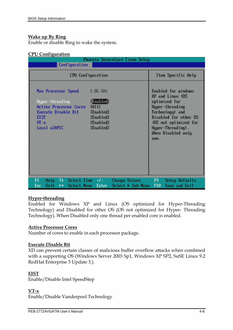
Wake up By Ring Enable or disable Ring to wake the system. CPU Configuration
Hyper-threading Enabled for Windows XP and Linux (OS optimized for Hyper-Threading Technology) and Disabled for other OS (OS not optimized for Hyper- Threading Technology). When Disabled only one thread per enabled core is enabled. Active Processor Cores Number of cores to enable in each processor package. Execute Disable Bit XD can prevent certain classes of malicious buffer overflow attacks when combined with a supporting OS (Windows Server 2003 Sp1, Windows XP SP2, SuSE Linux 9.2 RedHat Enterprise 3 Update 3.). EIST Enable/Disable Intel SpeedStep VT-x Enable/Disable Vanderpool Technology

BIOS Setup Information
PEB-2772AVGATM User’s Manual 4-9
Local x2APIC Enable Local x2APIC. Some 0Ses do not support this. LAN Configuration
Wake on LAN Enable or disable integrated LAN to wake the system. LAN Boot ROM Enable or disable integrated LAN Boot ROM(PXE) function.
BIOS Setup Information
PEB-2772AVGATM User’s Manual 4-10
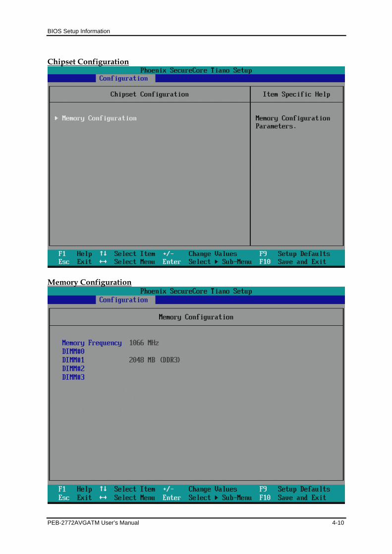
Chipset Configuration
Memory Configuration

BIOS Setup Information
PEB-2772AVGATM User’s Manual 4-11
Graphic Configuration
Primary Display Select which of IGFX/PEG/PCI Graphics device should be Primary Display or select SG for Switchable Gfx. The choice: Auto, IGFX, PEG, PCI Boot Display Select the video Device which will be activated during POST. This has no effect if external graphics present. Secondary boot display selection will appear based on your selection. VGA modes will be supported only on primary display. Choices: CRT, LVDS, CRT+LVDS, CRT+HDMI, LVDS + HDMI LVDS Panel Type Select LCD Panel used by internal Graphics by selecting the appropriate setup item. Choices: 800x600, 1024x768, 1280x800, 1280x1024, 1920x1080
BIOS Setup Information
PEB-2772AVGATM User’s Manual 4-12
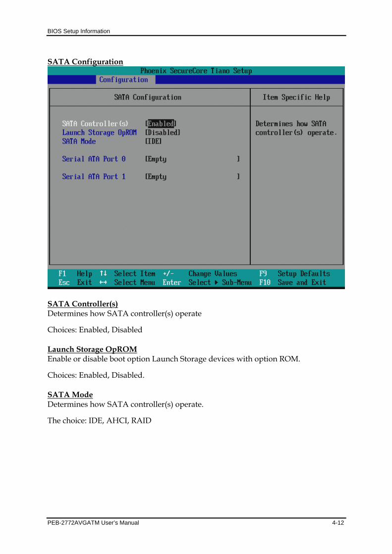
SATA Configuration
SATA Controller(s) Determines how SATA controller(s) operate
Choices: Enabled, Disabled Launch Storage OpROM Enable or disable boot option Launch Storage devices with option ROM.
Choices: Enabled, Disabled. SATA Mode Determines how SATA controller(s) operate.
The choice: IDE, AHCI, RAID
BIOS Setup Information
PEB-2772AVGATM User’s Manual 4-13
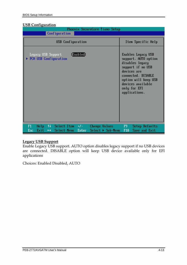
USB Configuration
Legacy USB Support Enable Legacy USB support. AUTO option disables legacy support if no USB devices are connected. DISABLE option will keep USB device available only for EFI applications
Choices: Enabled Disabled, AUTO

BIOS Setup Information
PEB-2772AVGATM User’s Manual 4-14
PCH USB Configuration
USB Ports Per-Port Disable Control each of the USB ports disabling
Choices: Enabled, Disabled USB Port #0~#6 Disable Disable selected USB port
Choices: Enabled, Disabed.

BIOS Setup Information
PEB-2772AVGATM User’s Manual 4-15
SIO Configuration
BIOS Setup Information
PEB-2772AVGATM User’s Manual 4-16
On Board Serial Port 1 Choices: Enabled, Disabled Base I/O Address Choices: 3F8, 2F8, 3E8, 2E8 Interrupt Choices: 3, 4, 5, 11 On Board Serial Port 2 Choices: Enabled, Disabled Base I/O Address Choices: 3F8, 2F8, 3E8, 2E8 Interrupt Choices: 3, 4, 5, 11 On Board Serial Port 3 Choices: Enabled, Disabled Base I/O Address Choices: 3F8, 2F8, 3E8, 2E8 Interrupt Choices: 3, 4, 5, 11 On Board Serial Port 4 Choices: Enabled, Disabled Base I/O Address Choices: 3F8, 2F8, 3E8, 2E8 Interrupt Choices: 3, 4, 5, 11 Watch Dog Timer Select Choices: Disable, 15secs, 30secs, 1min, 2mins, 3mins Case Open Control Choices: Enabled, Disabled, Power Loss Choices: Off, On, Former Status.

BIOS Setup Information
PEB-2772AVGATM User’s Manual 4-17
Hardware Monitor
Smart Fan Control
BIOS Setup Information
PEB-2772AVGATM User’s Manual 4-18
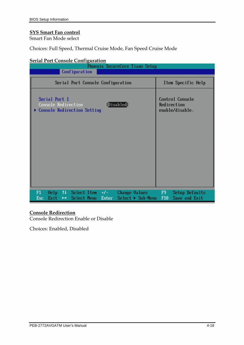
SYS Smart Fan control Smart Fan Mode select
Choices: Full Speed, Thermal Cruise Mode, Fan Speed Cruise Mode Serial Port Console Configuration
Console Redirection Console Redirection Enable or Disable
Choices: Enabled, Disabled
BIOS Setup Information
PEB-2772AVGATM User’s Manual 4-19
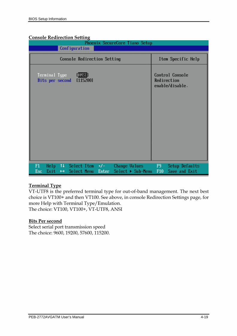
Console Redirection Setting
Terminal Type VT-UTF8 is the preferred terminal type for out-of-band management. The next best choice is VT100+ and then VT100. See above, in console Redirection Settings page, for more Help with Terminal Type/Emulation. The choice: VT100, VT100+, VT-UTF8, ANSI Bits Per second Select serial port transmission speed The choice: 9600, 19200, 57600, 115200.

BIOS Setup Information
PEB-2772AVGATM User’s Manual 4-20
4.4 Security This section lets you set security passwords to control access to the system at boot time and/or when entering the BIOS setup program. Some systems have a single password, while many newer ones now have two: a supervisor and a user password.
Set Supervisor/User Password Set or Clear Supervisor Password Supervisor/User Hint String Enter to type Supervisor/User Hint String Flash Controller Lock Lock all flash controllers The choice: Enabled, Disabled.
BIOS Setup Information
PEB-2772AVGATM User’s Manual 4-21
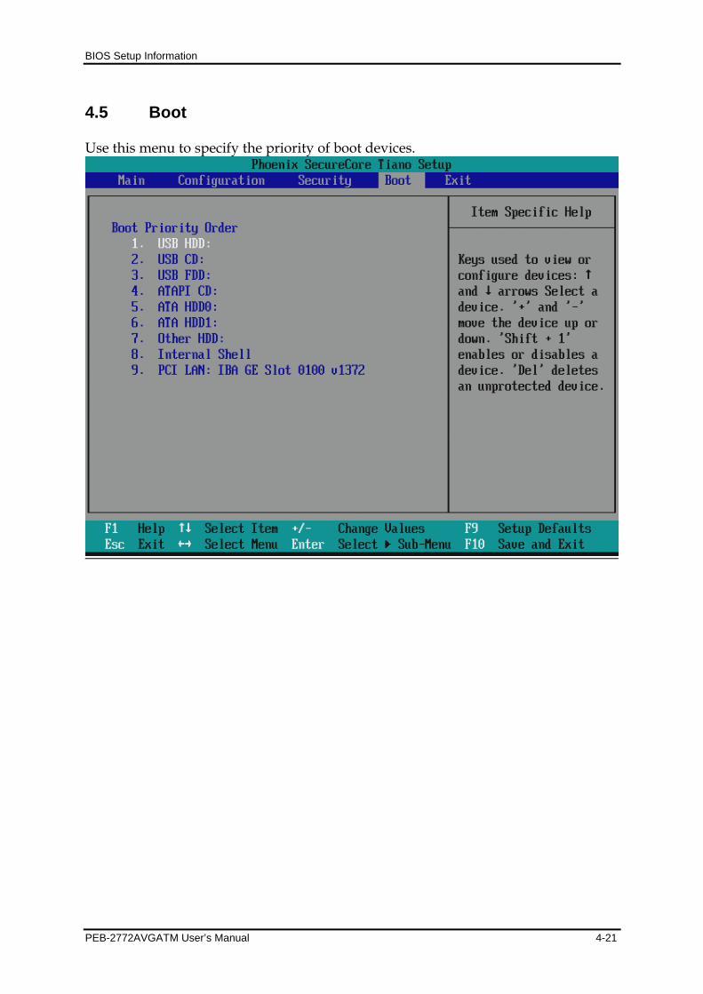
4.5 Boot Use this menu to specify the priority of boot devices.

BIOS Setup Information
PEB-2772AVGATM User’s Manual 4-22
4.6 Security This menu allows you to load the BIOS default values or factory default settings into the BIOS and exit the BIOS setup utility with or without changes.
Exit Saving Changes Exit system setup after saving the changes. Exit Discarding Changes Exit system setup without saving the changes. Load Setup Defaults Restore the User Defaults to all the setup options. Discard Changes Discard Changes done so far to any of the setup options. Save Changes Save Changes done so far to any of the setup options.
Troubleshooting
PEB-2772AVGATM User’s Manual 5-1
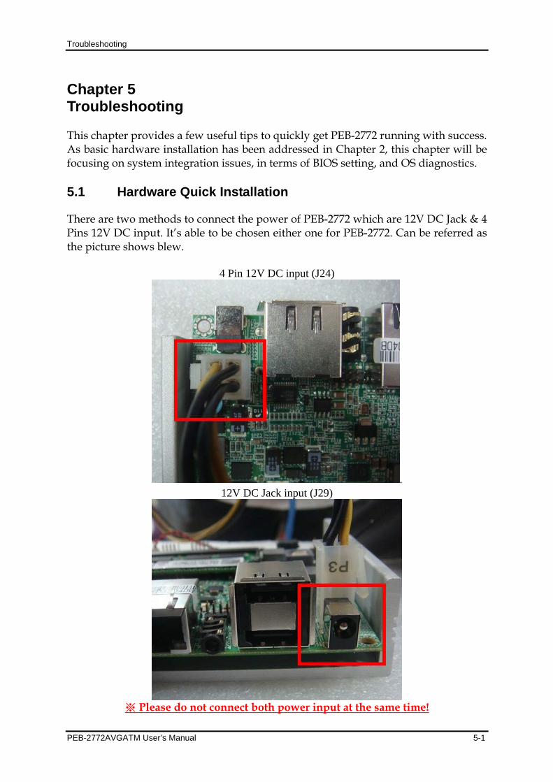
Chapter 5 Troubleshooting This chapter provides a few useful tips to quickly get PEB-2772 running with success. As basic hardware installation has been addressed in Chapter 2, this chapter will be focusing on system integration issues, in terms of BIOS setting, and OS diagnostics. 5.1 Hardware Quick Installation There are two methods to connect the power of PEB-2772 which are 12V DC Jack & 4 Pins 12V DC input. It’s able to be chosen either one for PEB-2772. Can be referred as the picture shows blew.
4 Pin 12V DC input (J24)
. 12V DC Jack input (J29)
※ Please do not connect both power input at the same time!

Troubleshooting
PEB-2772AVGATM User’s Manual 5-2
Please also make sure every other necessary devices are connected before hooking up power source. Loading the default optimal setting When prompted with the main setup menu, please scroll down to “Load Setup Defaults”, press “Enter” and “Y” to load in default optimal BIOS setup. This will force your BIOS setting back to the initial factory configuration. It is recommended to do this so you can be sure the system is running with the BIOS setting that Portwell has highly endorsed. As a matter of fact, users can load the default BIOS setting any time when system appears to be unstable in boot up sequence. 5.2 FAQ Question: I forget my password of system BIOS, what am I supposed to do? Answer: You can simply short 2-3 pins on J22 to clean your password. Question: I cannot boot up my system! Answer: Please make sure all the setups were followed the instruction in User’s manual. Unplugged any other add-on device to isolate the possibility of external affection and try again. If the SBC still does not boot, please contact with our Technical support department. Note: Please visit our technical web site at http://www.portwell.com.tw For additional technical information, which is not covered in this manual, you can mail to [email protected] or you can also send mail to our sales, they wull be very delighted to forward them to us.

Troubleshooting
PEB-2772AVGATM User’s Manual 5-3
System Memory Address Map Each On-board device in the system is assigned a set of memory addresses, which also can be identical of the device. The following table lists the system memory address used for your reference.
System Memory Address Map Memory Area Size Description
0000-003F 1K Interrupt Area 0040-004F 0.3K BIOS Data Area 0050-006F 0.5K System Data 0070-0566 19K DOS 0567-0FE0 41K Program Area
0FE1-9DBF 567K 【Available】 First Meg -- Conventional memory end at 624K --
9FC0-9FFF 1K Extended BIOS Area A000-AFFF 64K VGA Graphics B000-B7FF 32K Unused B800-BFFF 32K VGA Text C000-CEFF 60K Video ROM CF00-EFFF 132K Unused F000-FFFF 64K System ROM
HMA 64K First 64K Extended

Troubleshooting
PEB-2772AVGATM User’s Manual 5-4
Interrupt Request Lines (IRQ) Peripheral devices can use interrupt request lines to notify CPU for the service required. The following table shows the IRQ used by the devices on board.
Interrupt Request Lines IRQ IRQ# Current Use Default Use IRQ 0 System ROM System Timer IRQ 1 System ROM Keyboard Event IRQ 2 【Unassigned】 Usable IRQ IRQ 3 System ROM COM2 IRQ 4 System ROM COM1 IRQ 5 【Unassigned】 Usable IRQ IRQ 6 System ROM Diskette Event IRQ 7 【Unassigned】 Usable IRQ IRQ 8 System ROM Real-Time Clock IRQ 9 【Unassigned】 Usable IRQ IRQ 10 【Unassigned】 Usable IRQ IRQ 11 Video ROM Usable IRQ IRQ 12 System ROM IBM Mouse Event IRQ 13 System ROM Coprocessor Error IRQ 14 System ROM Hard Disk Event IRQ 15 【Unassigned】 Usable IRQ