Thin Film Tour - API Technologiesmicro.apitech.com/pdf/tours/thinFilmTour.pdfcoupler lines and ......
30
ADVANCED THIN FILM TECHNOLOGIES TOUR
Transcript of Thin Film Tour - API Technologiesmicro.apitech.com/pdf/tours/thinFilmTour.pdfcoupler lines and ......

ADVANCED THIN FILM TECHNOLOGIES
TOUR

2
• Provider of technically demanding RF/microwave, electromagnetic, power, and security solutions for defense, aerospace and commercial industries
• Founded in 1981; Listed on NASDAQ June 2011 with a new company vision
– Today, one of the largest non-Prime provider of RF/Microwave and microelectronics
• 1,975 employees worldwide • 3,000+ customers worldwide • Revenue breakdown
– ~75% Domestic / 25% International – ~60% Defense & Government / 40% Commercial
COMPANY OVERVIEW

OUR FOOTPRINT
3
Europe North America Asia
Design & Manufacturing Manufacturing Center Sales Office Design Center
• 12 Trusted facilities worldwide (US, UK, Canada)
• Technology focused: Nearly 20% of our employees are engineers and skilled design professionals
• International manufacturing locations are API companies - not subcontractors; same equipment and processes as U.S.
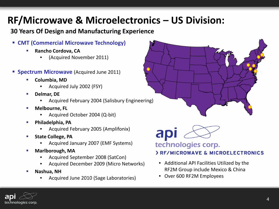
RF/Microwave & Microelectronics – US Division:
4
CMT (Commercial Microwave Technology) Rancho Cordova, CA
• (Acquired November 2011) Spectrum Microwave (Acquired June 2011)
Columbia, MD • Acquired July 2002 (FSY)
Delmar, DE • Acquired February 2004 (Salisbury Engineering)
Melbourne, FL • Acquired October 2004 (Q-bit)
Philadelphia, PA • Acquired February 2005 (Amplifonix)
State College, PA • Acquired January 2007 (EMF Systems)
Marlborough, MA • Acquired September 2008 (SatCon) • Acquired December 2009 (Micro Networks)
Nashua, NH • Acquired June 2010 (Sage Laboratories)
30 Years Of Design and Manufacturing Experience
• Additional API Facilities Utilized by the RF2M Group include Mexico & China
• Over 600 RF2M Employees

WORLD-CLASS FACILITY
5
API Benefits • 30,000 square feet of Class 100,000 Clean Room • Prototypes, Production and Qualification • Reduce Size/Lower Weight • Improve Performance and Reliability • Full Temperature Testing • Environmental Stress Screening • MIL-PRF-38534 Class H / K
API Technologies 45,000 ft2 facility to support the combined manufacturing and engineering operations of our Worcester and Marlborough facilities, located in the Marlborough, Massachusetts Technology Park. The facility is AS9100 registered and fully certified to MIL-PRF-38534 Class H and Class K standards. API is a designer and manufacturer of RF/microwave and hybrid components, microwave, MMW, and microelectronic assemblies for defense, space systems, satellite, high-rel commercial, communications, avionics and ruggedized industrial applications.

KEY SUPPLIER TO SATELLITE/SPACE PROGRAMS
6
Only 19 facilities worldwide have MIL-PRF-38534 Class K (Space) certification. Two of them are ours.
Deep Space • Galileo • Cassini • USERS • Mars Phoenix • OCO • LCROSS • Mars Satellite Lab • ISS Kibo EF
Scientific Missions • SAOCOM • Hershel Plank • Grail • EnMap • AMS-02 • Lisa Pathfinder • Meteosat • Juno
Communications • Sirius Radio • DirectTV • Olympus • Optus 10 • Amazonas 3 • GPS-2F • Thor 7 • MUOS • Inmarsat • Intelsat • Hot Bird
Launch & Reentry • Curiosity • Taurus • Minuteman • HII

COMPLETE SOLUTION PROVIDER
7
• Mixed Signal & Power • RF, Microwave & MMW • Optoelectronics • Space • Thin Film / SAW Wafer • Power Conversion / Regulation
Technologies
•Defense (MIL-PRF-38534 Class H) •Space (MIL-PRF-38534 Class K) •Avionics •Hi-Rel Commercial •Ruggedized Industrial •Secure Communications
Markets
•Advanced Engineering •High Density Manufacturing •DC-50 GHz •High Reliability •Class K Certified Facility •Thin Film / SAW Wafer Fab
Capabilities

THIN FILM & SAW FAB
8
Capabilities • Laser Cutting • Metal Deposition • Photo Lithography • Auto Step
Reticle Stepper • Precision Photo Resist • Automated Developer
Application • Ion Etching • Pack • Auto Probe & Trim • Auto Wafer Dicing • Active or Passive
Laser Trim

9
ADVANCED THIN FILM TECHNOLOGIES
Over 4 Decades of Thin Film Experience
API Technologies provides a complete solution for thin film products. API has extensive experience with thin film design, manufacturing and quality. Our thin film capabilities include multiple substrate materials, conductor and resistor layers of various materials, plated through and filled interconnects, protective coatings and laser trimming, among others. API engages with our customers from design concept and layout assistance, prototype development and full production support.
10
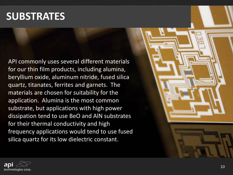
API commonly uses several different materials for our thin film products, including alumina, beryllium oxide, aluminum nitride, fused silica quartz, titanates, ferrites and garnets. The materials are chosen for suitability for the application. Alumina is the most common substrate, but applications with high power dissipation tend to use BeO and AlN substrates for their thermal conductivity and high frequency applications would tend to use fused silica quartz for its low dielectric constant.
SUBSTRATES

11
SUBSTRATES TYPICAL PROPERTIES OF COMMON THIN FILM SUBSTRATES

12
Metal schemes include Gold, Copper, Nickel, Titanium Tungsten, Nichrom and Tantalum Nitride lines/spaces to ± 0.000050".
Gold plated or metallized vias for improved ground plane connection or heat dissipation.
BeO, Alumina, Aluminum Nitride, Silicon and Ferrites are just some of the substrate materials available.
Selective 360˚ deposition allows for Gold to be deposited with a thickness of 100-400 micro inches.
THIN FILM TECHNOLOGIES

13
RESISTOR FILM PROPERTIES

14
Vias API Technologies offer plated through vias, gold filled vias and copper filled vias. These vias allow for excellent electrical and thermal paths to the ground plane, which will provide better performance for the intended application. Filled vias provide better electrical and thermal conductivity for RF/Microwave than plated through holes, and are preferable for high power applications. Filled vias and plated through holes both provide electrical connections to the ground plane and interconnects for thin film substrates with patterns on both sides of the substrate.

15
COPPER FILLED VIAS
• Copper filled vias provide a cost efficient solution to rising costs as the price of gold has risen more than 300% over the last decade.
• Copper technology offers increased thermal and electrical conductivity over gold.
• Copper filled vias are the preferred technology available for commercial packaging, hybrid manufacturers, and microelectronics providers in need of a high reliability and high conductivity substrate.

FILLED VIAS vs. PLATED THROUGH HOLES
16
• Filled vias provide higher conductivity and better thermal conductivity for RF/Microwave than plated through holes, and are preferable for high power applications.
• Filled vias and plated through holes both provide electrical connections to the ground plane in thin film substrates (also on PWBs/PCBs and thick film). Also, it provides interconnects for thin film substrates with patterns on both sides of the substrates.

17
Polyimide can be customized to meet a variety of shapes and dimensions, thereby providing versatility and flexibility with your design requests.
Adding a second layer of Polyimide helps protect the delicate bridge from structural damage during the assembly process.
Polyimide, which when added traditionally allows for repeatable coupler lines and spaces as small as 0.0006".
Another example of adding value through innovation is found while utilizing Polyimide for bridges and dams. The advantage of poly bridges over traditional air bridges is that non-conductive polyimide adds a level of support preventing the bridge from collapsing onto the circuit below. We have taken that process one step further by adding a second layer of polyimide on top of the bridge, complementing the foundation of structural integrity added to the bridge process by the base Polyimide layer.
POLYMIDE BRIDGES & DAMS

18
Sputtering Capabilities With over 4 decades of sputtering experience, we are the premier
choice for thin film metallization solutions. • Titanium Tungsten • Gold • Nickel • Copper • Platinum • Aluminum • Chromium • Silver • Palladium
ADVANCED THIN FILM TECHNOLOGIES

19
Sputtering Equipment • KDF954 • KDF943 • MRC954
• Load lock systems • 12” x 12” pallette size
• Multiple sputtering systems with multiple targets
• Improved lead times with reduced target changes
Process • Alkaline cleaning with
DI water rinse • 12” x 10” sweet spot
ADVANCED THIN FILM TECHNOLOGIES

20
ADVANCED THIN FILM TECHNOLOGIES
Photolithography and Etching • Positive Resist • Wet etching available for Au, TiW, Ta, NiCr, Ni, Cu, Ti, SiO2 • Minimum Geometrical Etching
• Conductors: 0.6 mils (0.1 tolerance) • Resistors: 0.2 mils (0.04)

21
ADVANCED THIN FILM TECHNOLOGIES Design Guide Thin Film Metallized Substrates This useful layout guide, with its accompanying metals and their functions outline, should help serve as a resource for both the CAD specialists, as well as the engineer involved in the design of the substrate or PC board. Helpful resistor values along with material types and their range of functions is included and is another example of why API Technologies leads the industry in both innovation AND customer service.

22
THIN FILM CHIP RESISTORS
API offers a wide variety of thin film chip resistors as standard products. There are multiple options available that provide options for substrate material, resistor material, temperature coefficient of resistance, resistor value and tolerance and size.

23
THIN FILM CHIP RESISTORS
Core Competencies • Silicon or alumina substrate • Resistor tolerance 0.1% • Back side contact options • Pre-soldered options • Tantalum Nitride or Nickel Chrome resistor
materials • Passivation as required
Processing Steps • 100% sputter thin film • Conductor and resistor photolithography
and etch • Stabilization • YAG laser trim • Passivation as required • 100% Visual inspection
Chip Resistor Sizes • Single Tap .020 x .020 Series • Single Tap .020 x .040 Series • Single Tap .030 x .030 Series • Center Tap .030 x .030 Series • Multi Tap .030 x .030 Series • Single Tap .040 x .040 Series • Single Tap .050 x .050 Series • Single Tap .050 x .100 Series
24
ADVANCED THIN FILM TECHNOLOGIES
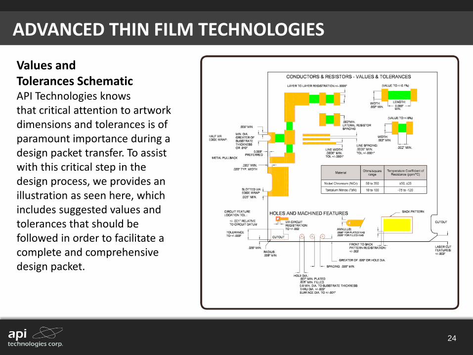
Values and Tolerances Schematic API Technologies knows that critical attention to artwork dimensions and tolerances is of paramount importance during a design packet transfer. To assist with this critical step in the design process, we provides an illustration as seen here, which includes suggested values and tolerances that should be followed in order to facilitate a complete and comprehensive design packet.

• AS9100:2009 Certified - DNV
• MIL-PRF-38534 Certified and Qualified - DLA Land and Maritime o MIL-PRF-38534, Class K and H Certified Hybrid Microcircuits o MIL-PRF-38534, QML-38534 Qualified Processes and Materials o MIL-PRF-38534, Thin Film Chip Resistor & Substrate Fab o MIL-STD-883 Test Methods - DLA Lab Suitability
• Other Specifications Guidelines o J-STD-001 o IPC-A-610
• Quality Assurance Programs o Calibration Recall System for Test and Measurement Equipment o ESD Program o Failure Analysis and Corrective Action System o AS9100 and MIL-PRF-38534 Internal Audit Program o Operator Training and Recertification Program
25
QUALITY AND RELIABILITY – Marlborough Facility

26

27

28
QUALITY CONTROL API’s Thin Film products all have the highest quality screenings which will provide assurances of performance and reliability for any application.
• MIL-PRF-38534 • Class H and K • AS9100 • In-House Thin Film Fabrication Line

29
Specification Development
Simulation & Design
Prototyping
Testing
Logistics
Manufacturing
1 2
3
4 5
6
DESIGN & DEVELOPMENT PROCESS

Custom Thin Film Substrates & Thin Film Chip Resistors Points of Contact
30
Paul Possemato Microelectronics Business Development Manager [email protected] Michael Schweyer Product Line Manager [email protected] Mark Sullivan Engineering Manager [email protected]