8-bit - Digi-Key Sheets/Atmel PDFs...output port, each pin can sink eight TTL inputs. When 1s are...
25
PLCC 7 8 9 10 11 12 13 14 15 16 17 39 38 37 36 35 34 33 32 31 30 29 P1.5 P1.6 P1.7 RST (RXD) P3.0 NC (TXD) P3.1 (INT0) P3.2 (INT1) P3.3 (T0) P3.4 (T1) P3.5 P0.4 (AD4) P0.5 (AD5) P0.6 (AD6) P0.7 (AD7) EA/VPP NC ALE/PROG PSEN P2.7 (A15) P2.6 (A14) P2.5 (A13) 6 5 4 3 2 1 44 43 42 41 40 18 19 20 21 22 23 24 25 26 27 28 (WR) P3.6 (RD) P3.7 XTAL2 XTAL1 GND NC (A8) P2.0 (A9) P2.1 (A10) P2.2 (A11) P2.3 (A12) P2.4 P1.4 P1.3 P1.2 P1.1 (T2 EX) P1.0 (T2) NC VCC P0.0 (AD0) P0.1 (AD1) P0.2 (AD2) P0.3 (AD3) Features • Compatible with MCS-51 ™ Products • 32K Bytes of One-time Programmable QuickFlash ™ Memory • 4V to 6V Operating Range • Fully Static Operation: 0 Hz to 24 MHz • Three-level Program Memory Lock • 512 x 8-bit Internal RAM • 32 Programmable I/O Lines • Three 16-bit Timer/Counters • Eight Interrupt Sources • Programmable Serial Channel • Low-power Idle and Power-down Modes • Interrupt Recovery from Power-down • Hardware Watchdog Timer • Dual Data Pointer • Power-off Flag Description The AT87F51RC is a low-power, high-performance CMOS 8-bit microcomputer with 32K bytes of QuickFlash one-time programmable (OTP) read only memory and 512 bytes of RAM. The device is manufactured using Atmel’s high-density nonvolatile memory technology and is compatible with the industry-standard 80C51 and 80C52 instruction set and pinout. The on-chip QuickFlash allows the program memory to be Rev. 1106C–02/00 8-bit Microcontroller with 32K Bytes QuickFlash™ AT87F51RC PDIP 1 2 3 4 5 6 7 8 9 10 11 12 13 14 15 16 17 18 19 20 40 39 38 37 36 35 34 33 32 31 30 29 28 27 26 25 24 23 22 21 (T2) P1.0 (T2EX) P1.1 P1.2 P1.3 P1.4 P1.5 P1.6 P1.7 RST (RXD) P3.0 (TXD) P3.1 (INT0) P3.2 (INT1) P3.3 (T0) P3.4 (T1) P3.5 (WR) P3.6 (RD) P3.7 XTAL2 XTAL1 GND VCC P0.0 (AD0) P0.1 (AD1) P0.2 (AD2) P0.3 (AD3) P0.4 (AD4) P0.5 (AD5) P0.6 (AD6) P0.7 (AD7) EA/VPP ALE/PROG PSEN P2.7 (A15) P2.6 (A14) P2.5 (A13) P2.4 (A12) P2.3 (A11) P2.2 (A10) P2.1 (A9) P2.0 (A8) Pin Configurations TQFP 1 2 3 4 5 6 7 8 9 10 11 33 32 31 30 29 28 27 26 25 24 23 P1.5 P1.6 P1.7 RST (RXD) P3.0 NC (TXD) P3.1 (INT0) P3.2 (INT1) P3.3 (T0) P3.4 (T1) P3.5 P0.4 (AD4) P0.5 (AD5) P0.6 (AD6) P0.7 (AD7) EA/VPP NC ALE/PROG PSEN P2.7 (A15) P2.6 (A14) P2.5 (A13) 44 43 42 41 40 39 38 37 36 35 34 12 13 14 15 16 17 18 19 20 21 22 (WR) P3.6 (RD) P3.7 XTAL2 XTAL1 GND GND (A8) P2.0 (A9) P2.1 (A10) P2.2 (A11) P2.3 (A12) P2.4 P1.4 P1.3 P1.2 P1.1 (T2 EX) P1.0 (T2) NC VCC P0.0 (AD0) P0.1 (AD1) P0.2 (AD2) P0.3 (AD3)
Transcript of 8-bit - Digi-Key Sheets/Atmel PDFs...output port, each pin can sink eight TTL inputs. When 1s are...

8-bit Microcontroller with 32K Bytes QuickFlash™
AT87F51RC
Features• Compatible with MCS-51™ Products• 32K Bytes of One-time Programmable QuickFlash™ Memory• 4V to 6V Operating Range• Fully Static Operation: 0 Hz to 24 MHz• Three-level Program Memory Lock• 512 x 8-bit Internal RAM• 32 Programmable I/O Lines• Three 16-bit Timer/Counters• Eight Interrupt Sources• Programmable Serial Channel• Low-power Idle and Power-down Modes• Interrupt Recovery from Power-down• Hardware Watchdog Timer• Dual Data Pointer• Power-off Flag
DescriptionThe AT87F51RC is a low-power, high-performance CMOS 8-bit microcomputer with32K bytes of QuickFlash one-time programmable (OTP) read only memory and 512bytes of RAM. The device is manufactured using Atmel’s high-density nonvolatilememory technology and is compatible with the industry-standard 80C51 and 80C52instruction set and pinout. The on-chip QuickFlash allows the program memory to be
1
PLCC
7891011121314151617
3938373635343332313029
P1.5P1.6P1.7RST
(RXD) P3.0NC
(TXD) P3.1(INT0) P3.2(INT1) P3.3
(T0) P3.4(T1) P3.5
P0.4 (AD4)P0.5 (AD5)P0.6 (AD6)P0.7 (AD7)EA/VPPNCALE/PROGPSENP2.7 (A15)P2.6 (A14)P2.5 (A13)
6 5 4 3 2 1 44 43 42 41 40
18 19 20 21 22 23 24 25 26 27 28
(WR
) P
3.6
(RD
) P
3.7
XT
AL2
XT
AL1
GN
DN
C(A
8) P
2.0
(A9)
P2.
1(A
10)
P2.
2(A
11)
P2.
3(A
12)
P2.
4
P1.
4P
1.3
P1.
2P
1.1
(T2
EX
)P
1.0
(T2)
NC
VC
CP
0.0
(AD
0)P
0.1
(AD
1)P
0.2
(AD
2)P
0.3
(AD
3)
Rev. 1106C–02/00
PDIP
1234567891011121314151617181920
4039383736353433323130292827262524232221
(T2) P1.0(T2EX) P1.1
P1.2P1.3P1.4P1.5P1.6P1.7RST
(RXD) P3.0(TXD) P3.1(INT0) P3.2(INT1) P3.3
(T0) P3.4(T1) P3.5
(WR) P3.6(RD) P3.7
XTAL2XTAL1
GND
VCCP0.0 (AD0)P0.1 (AD1)P0.2 (AD2)P0.3 (AD3)P0.4 (AD4)P0.5 (AD5)P0.6 (AD6)P0.7 (AD7)EA/VPPALE/PROGPSENP2.7 (A15)P2.6 (A14)P2.5 (A13)P2.4 (A12)P2.3 (A11)P2.2 (A10)P2.1 (A9)P2.0 (A8)
Pin Configurations
TQFP
1234567891011
3332313029282726252423
P1.5P1.6P1.7RST
(RXD) P3.0NC
(TXD) P3.1(INT0) P3.2(INT1) P3.3
(T0) P3.4(T1) P3.5
P0.4 (AD4)P0.5 (AD5)P0.6 (AD6)P0.7 (AD7)EA/VPPNCALE/PROGPSENP2.7 (A15)P2.6 (A14)P2.5 (A13)
44 43 42 41 40 39 38 37 36 35 34
12 13 14 15 16 17 18 19 20 21 22
(WR
) P
3.6
(RD
) P
3.7
XT
AL2
XT
AL1
GN
DG
ND
(A8)
P2.
0(A
9) P
2.1
(A10
) P
2.2
(A11
) P
2.3
(A12
) P
2.4
P1.
4P
1.3
P1.
2P
1.1
(T2
EX
)P
1.0
(T2)
NC
VC
CP
0.0
(AD
0)P
0.1
(AD
1)P
0.2
(AD
2)P
0.3
(AD
3)

user programmed by a conventional nonvolatile memoryprogrammer. A total of 512 bytes of internal RAM are avail-able in the AT87F51RC. The 256-byte expanded internalRAM is accessed via MOVX instructions after clearing bit 1in the SFR located at address 8EH. The other 256-byteRAM segment is accessed the same way as the Atmel
AT89-series and other 8052-compatible products. By com-bining a versatile 8-bit CPU with QuickFlash on a mono-l i th ic ch ip , the A tmel AT87F51RC is a power fu lmicrocomputer which provides a highly-flexible and cost-effective solution to many embedded control applications.
Block Diagram
PORT 2 DRIVERS
PORT 2LATCH
P2.0 - P2.7
QUICKFLASH
PORT 0LATCHRAM
PROGRAMADDRESSREGISTER
BUFFER
PCINCREMENTER
PROGRAMCOUNTER
DUALDPTR
RAM ADDR.REGISTER
INSTRUCTIONREGISTER
BREGISTER
INTERRUPT, SERIAL PORT,AND TIMER BLOCKS
STACKPOINTERACC
TMP2 TMP1
ALU
PSW
TIMINGAND
CONTROL
PORT 3LATCH
PORT 3 DRIVERS
P3.0 - P3.7
PORT 1LATCH
PORT 1 DRIVERS
P1.0 - P1.7
OSC
GND
VCC
PSEN
ALE/PROG
EA / VPP
RST
PORT 0 DRIVERS
P0.0 - P0.7
WATCHDOG
AT87F51RC2

AT87F51RC
The AT87F51RC provides the following standard features:32K bytes of QuickFlash, 512 bytes of RAM, 32 I/O lines,three 16-bit timer/counters, a six-vector two-level interruptarchitecture, a full duplex serial port, on-chip oscillator, andclock circuitry. In addition, the AT87F51RC is designedwith static logic for operation down to zero frequency andsupports two software selectable power saving modes. TheIdle Mode stops the CPU while allowing the RAM,timer/counters, serial port, and interrupt system to continuefunctioning. The Power-down mode saves the RAM con-tents but freezes the oscillator, disabling all other chip func-tions until the next external interrupt or hardware reset.
Pin DescriptionVCCSupply voltage.
GNDGround.
Port 0Port 0 is an 8-bit open drain bidirectional I/O port. As anoutput port, each pin can sink eight TTL inputs. When 1sare written to port 0 pins, the pins can be used as high-impedance inputs.
Port 0 can also be configured to be the multiplexed low-order address/data bus during accesses to external pro-gram and data memory. In this mode, P0 has internal pul-lups.
Port 0 also receives the code bytes during QuickFlash pro-gramming and outputs the code bytes during program veri-fication. External pullups are required during programverification.
Port 1Port 1 is an 8-bit bidirectional I/O port with internal pullups.The Port 1 output buffers can sink/source four TTL inputs.When 1s are written to Port 1 pins, they are pulled high bythe internal pullups and can be used as inputs. As inputs,Port 1 pins that are externally being pulled low will sourcecurrent (IIL) because of the internal pullups.
In addition, P1.0 and P1.1 can be configured to be thetimer/counter 2 external count input (P1.0/T2) and thetimer/counter 2 trigger input (P1.1/T2EX), respectively, asshown in the following table.
Port 1 also receives the low-order address bytes duringQuickFlash programming and verification.
Port 2Port 2 is an 8-bit bidirectional I/O port with internal pullups.The Port 2 output buffers can sink/source four TTL inputs.When 1s are written to Port 2 pins, they are pulled high bythe internal pullups and can be used as inputs. As inputs,Port 2 pins that are externally being pulled low will sourcecurrent (IIL) because of the internal pullups.
Port 2 emits the high-order address byte during fetchesfrom external program memory and during accesses toexternal data memory that use 16-bit addresses (MOVX @DPTR). In this application, Port 2 uses strong internal pul-lups when emitting 1s. During accesses to external datamemory that use 8-bit addresses (MOVX @ RI), Port 2emits the contents of the P2 Special Function Register.
Port 2 also receives the high-order address bits and somecontrol signals during QuickFlash programming and verifi-cation.
Port 3Port 3 is an 8-bit bidirectional I/O port with internal pullups.The Port 3 output buffers can sink/source four TTL inputs.When 1s are written to Port 3 pins, they are pulled high bythe internal pullups and can be used as inputs. As inputs,Port 3 pins that are externally being pulled low will sourcecurrent (IIL) because of the pullups.
Port 3 also serves the functions of various special featuresof the AT87F51RC, as shown in the following table.
Port 3 also receives some control signals for QuickFlashprogramming and verification.
RSTReset input. A high on this pin for two machine cycles whilethe oscillator is running resets the device. This pin drivesHigh for 96 oscillator periods after the Watchdog times out.The DISRTO bit in SFR AUXR (address 8EH) can be usedto disable this feature. In the default state of bit DISTRO,the RESET HIGH out feature is enabled.
ALE/PROGAddress Latch Enable is an output pulse for latching thelow byte of the address during accesses to external
Port Pin Alternate Functions
P1.0T2 (external count input to Timer/Counter 2), clock-out
P1.1T2EX (Timer/Counter 2 capture/reload trigger and direction control)
Port Pin Alternate Functions
P3.0 RXD (serial input port)
P3.1 TXD (serial output port)
P3.2 INT0 (external interrupt 0)
P3.3 INT1 (external interrupt 1)
P3.4 T0 (timer 0 external input)
P3.5 T1 (timer 1 external input)
P3.6 WR (external data memory write strobe)
P3.7 RD (external data memory read strobe)
3

memory. This pin is also the program pulse input (PROG)during QuickFlash programming.
In normal operation, ALE is emitted at a constant rate of 1/6the oscillator frequency and may be used for externaltiming or clocking purposes. Note, however, that oneALE pulse is skipped during each access to external datamemory.
If desired, ALE operation can be disabled by setting bit 0 ofSFR location 8EH. With the bit set, ALE is active only dur-ing a MOVX or MOVC instruction. Otherwise, the pin isweakly pulled high. Setting the ALE-disable bit has noeffect if the microcontroller is in external execution mode.
PSENProgram Store Enable is the read strobe to external pro-gram memory.
When the AT87F51RC is executing code from external pro-gram memory, PSEN is activated twice each machine
cycle, except that two PSEN activations are skipped duringeach access to external data memory.
EA/VPPExternal Access Enable. EA must be strapped to GND inorder to enable the device to fetch code from external pro-gram memory locations starting at 0000H up to FFFFH.Note, however, that if lock bit 1 is programmed, EA will beinternally latched on reset.
EA should be strapped to VCC for internal program execu-tions.
This pin also receives the 12-volt programming enable volt-age (VPP) during QuickFlash programming.
XTAL1Input to the inverting oscillator amplifier and input to theinternal clock operating circuit.
XTAL2Output from the inverting oscillator amplifier.
Table 1. AT87F51RC SFR Map and Reset Values
0F8H 0FFH
0F0HB
000000000F7H
0E8H 0EFH
0E0HACC
000000000E7H
0D8H 0DFH
0D0HPSW
000000000D7H
0C8HT2CON
00000000T2MOD
XXXXXX00RCAP2L00000000
RCAP2H00000000
TL200000000
TH200000000
0CFH
0C0H 0C7H
0B8HIP
XX0000000BFH
0B0HP3
111111110B7H
0A8HIE
0X0000000AFH
0A0HP2
11111111AUXR1
XXXXXXX0WDTRST
XXXXXXXX0A7H
98HSCON
00000000SBUF
XXXXXXXX9FH
90HP1
1111111197H
88HTCON
00000000TMOD
00000000TL0
00000000TL1
00000000TH0
00000000TH1
00000000AUXR
XXX000008FH
80HP0
11111111SP
00000111DP0L
00000000DP0H
00000000DP1L
00000000DP1H
00000000PCON
0XXX000087H
AT87F51RC4

AT87F51RC
Special Function RegistersA map of the on-chip memory area called the Special Func-tion Register (SFR) space is shown in Table 1.
Note that not all of the addresses are occupied, and unoc-cupied addresses may not be implemented on the chip.Read accesses to these addresses will in general returnrandom data, and write accesses will have an indetermi-nate effect.
User software should not write 1s to these unlisted loca-tions, since they may be used in future products to invoke
new features. In that case, the reset or inactive values ofthe new bits will always be 0.
Timer 2 Registers: Control and status bits are contained inregisters T2CON (shown in Table 2) and T2MOD (shown inTable 4) for Timer 2. The register pair (RCAP2H, RCAP2L)are the Capture/Reload registers for Timer 2 in 16-bit cap-ture mode or 16-bit auto-reload mode.
Interrupt Registers: The individual interrupt enable bitsare in the IE register. Two priorities can be set for each ofthe six interrupt sources in the IP register.
Table 2. T2CON – Timer/Counter 2 Control Register
T2CON Address = 0C8H Reset Value = 0000 0000B
Bit Addressable
Bit TF2 EXF2 RCLK TCLK EXEN2 TR2 C/T2 CP/RL2
7 6 5 4 3 2 1 0
Symbol Function
TF2 Timer 2 overflow flag set by a Timer 2 overflow and must be cleared by software. TF2 will not be set when either RCLK = 1 or TCLK = 1.
EXF2 Timer 2 external flag set when either a capture or reload is caused by a negative transition on T2EX and EXEN2 = 1. When Timer 2 interrupt is enabled, EXF2 = 1 will cause the CPU to vector to the Timer 2 interrupt routine. EXF2 must be cleared by software. EXF2 does not cause an interrupt in up/down counter mode (DCEN = 1).
RCLK Receive clock enable. When set, causes the serial port to use Timer 2 overflow pulses for its receive clock in serial port Modes 1 and 3. RCLK = 0 causes Timer 1 overflow to be used for the receive clock.
TCLK Transmit clock enable. When set, causes the serial port to use Timer 2 overflow pulses for its transmit clock in serial port Modes 1 and 3. TCLK = 0 causes Timer 1 overflows to be used for the transmit clock.
EXEN2 Timer 2 external enable. When set, allows a capture or reload to occur as a result of a negative transition on T2EX if Timer 2 is not being used to clock the serial port. EXEN2 = 0 causes Timer 2 to ignore events at T2EX.
TR2 Start/Stop control for Timer 2. TR2 = 1 starts the timer.
C/T2 Timer or counter select for Timer 2. C/T2 = 0 for timer function. C/T2 = 1 for external event counter (falling edge triggered).
CP/RL2 Capture/Reload select. CP/RL2 = 1 causes captures to occur on negative transitions at T2EX if EXEN2 = 1. CP/RL2 = 0 causes automatic reloads to occur when Timer 2 overflows or negative transitions occur at T2EX when EXEN2 = 1. When either RCLK or TCLK = 1, this bit is ignored and the timer is forced to auto-reload on Timer 2 overflow.
5
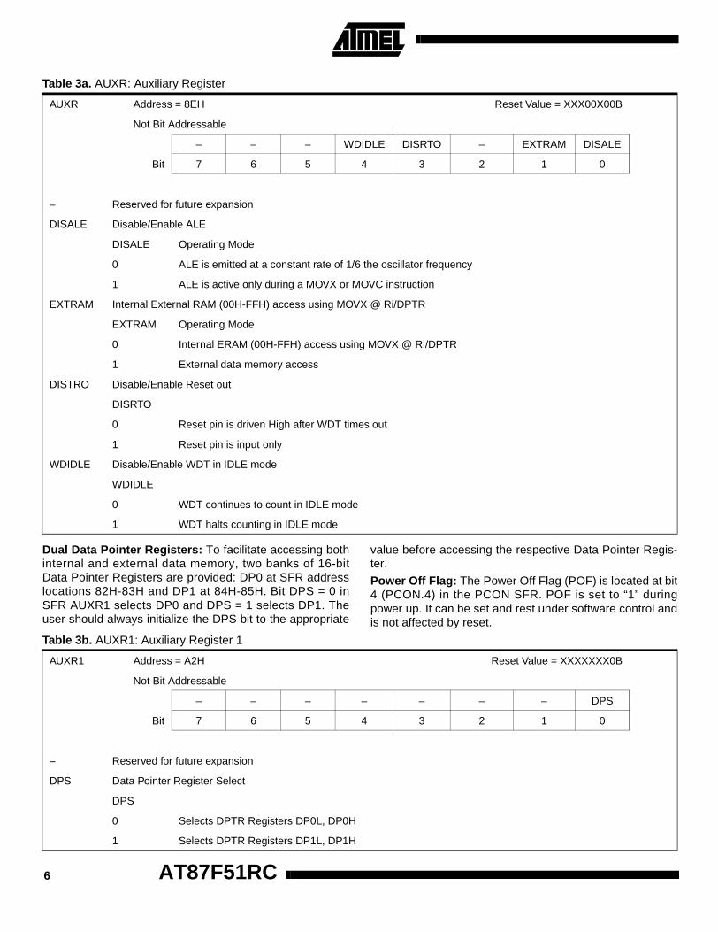
Dual Data Pointer Registers: To facilitate accessing bothinternal and external data memory, two banks of 16-bitData Pointer Registers are provided: DP0 at SFR addresslocations 82H-83H and DP1 at 84H-85H. Bit DPS = 0 inSFR AUXR1 selects DP0 and DPS = 1 selects DP1. Theuser should always initialize the DPS bit to the appropriate
value before accessing the respective Data Pointer Regis-ter.
Power Off Flag: The Power Off Flag (POF) is located at bit4 (PCON.4) in the PCON SFR. POF is set to “1” duringpower up. It can be set and rest under software control andis not affected by reset.
Table 3a. AUXR: Auxiliary Register
AUXR Address = 8EH Reset Value = XXX00X00B
Not Bit Addressable
– – – WDIDLE DISRTO – EXTRAM DISALE
Bit 7 6 5 4 3 2 1 0
– Reserved for future expansion
DISALE Disable/Enable ALE
DISALE Operating Mode
0 ALE is emitted at a constant rate of 1/6 the oscillator frequency
1 ALE is active only during a MOVX or MOVC instruction
EXTRAM Internal External RAM (00H-FFH) access using MOVX @ Ri/DPTR
EXTRAM Operating Mode
0 Internal ERAM (00H-FFH) access using MOVX @ Ri/DPTR
1 External data memory access
DISTRO Disable/Enable Reset out
DISRTO
0 Reset pin is driven High after WDT times out
1 Reset pin is input only
WDIDLE Disable/Enable WDT in IDLE mode
WDIDLE
0 WDT continues to count in IDLE mode
1 WDT halts counting in IDLE mode
Table 3b. AUXR1: Auxiliary Register 1
AUXR1 Address = A2H Reset Value = XXXXXXX0B
Not Bit Addressable
– – – – – – – DPS
Bit 7 6 5 4 3 2 1 0
– Reserved for future expansion
DPS Data Pointer Register Select
DPS
0 Selects DPTR Registers DP0L, DP0H
1 Selects DPTR Registers DP1L, DP1H
AT87F51RC6

AT87F51RC
Memory OrganizationMCS-51 devices have a separate address space for Pro-gram and Data Memory. Up to 64K bytes each of externalProgram and Data Memory can be addressed.
Program MemoryIf the EA pin is connected to GND, all program fetches aredirected to external memory.
On the AT87F51RC, if EA is connected to VCC, programfetches to addresses 0000H through 7FFFH are directed tointernal memory and fetches to addresses 8000H throughFFFFH are to external memory.
Data MemoryThe AT87F51RC has internal data memory that is mappedinto four separate segments: the lower 128 bytes of RAM,upper 128 bytes of RAM, 128 bytes special function regis-ter (SFR) and 256 bytes expanded RAM (ERAM).
The four segments are:
1. The Lower 128 bytes of RAM (addresses 00H to 7FH) are directly and indirectly addressable.
2. The Upper 128 bytes of RAM (addresses 80H to FFH) are indirectly addressable only.
3. The Special Function Registers, SFRs, (addresses 80H to FFH) are directly addressable only.
4. The 256-byte expanded RAM (ERAM, 00H-FFH) is indirectly accessed by MOVX instructions, and with the EXTRAM bit cleared.
The Lower 128 bytes can be accessed by either direct orindirect addressing. The Upper 128 bytes can be accessedby indirect addressing only. The Upper 128 bytes occupythe same address space as the SFR. This means theyhave the same address, but are physically separate fromthe SFR space.
When an instruction accesses an internal location aboveaddress 7FH, the CPU knows whether the access is to theupper 128 bytes of data RAM or to SFR space by theaddressing mode used in the instruction. Instructions thatuse direct addressing access SFR space. For example:
MOV 0A0H, # data
accesses the SFR at location 0S0H (which is P2). Instruc-tions that use indirect addressing access the Upper 128bytes of data RAM. For example:
MOV@R0, # data
where R0 contains 0A0H, accesses the data byte ataddress 0A0H, rather than P2 (whose address is 0A0H).
Note that stack operations are examples of indirectaddressing, so the upper 128 bytes of data RAM are avail-able as stack space.
The 256 bytes of ERAM can be accessed by indirectaddressing, with EXTRAM bit cleared and MOVX instruc-tions. This part of memory is physically located on-chip,logically occupying the first 256 bytes of external datamemory.
Figure 1. Internal and External Data Memory Address(with EXTRAM = 0)
With EXTRAM = 0, the ERAM is indirectly addressed,using the MOVX instruction in combination with any of theregisters R0, R1 of the selected bank or DPTR. An accessto ERAM will not affect ports P0, P2, P3.6 (WR), and P3.7(RD). For example, with EXTRAM = 0,
MOVX@R0, # data
where R0 contains 0A0H, accesses the ERAM at address0A0H rather than external memory. An access to externaldata memory locations higher than FFH (i.e. 0100H toFFFFH) will be performed with the MOVX DPTR instruc-tions in the same way as in the standard MCS-51, i.e., withP0 and P2 as data/address bus, and P3.6 and P3.7 aswrite and read timing signals. Refer to Figure 1.
With EXTRAM = 1, MOVX @ Ri and MOVX@DPTR will besimilar to the standard MCS-51. MOVX@Ri will provide an8-bit address multiplexed with data on Port 0 and any out-put port pins can be used to output higher-order addressbits. This is to provide the external paging capability.MOVX@DPTR will generate a 16-bit address. Port 2 out-puts the high-order 8 address bits (the contents of DP0H),while Port 0 multiplexes the low-order 8 address bits (thecontents o f DP0L) w i th da ta . MOVX@Ri andMOVX@DPTR will generate either read or write signals onP3.6 (WR) and P3.7 (RD).
The stack pointer (SP) may be located anywhere in the 256bytes RAM (lower and upper RAM) internal data memory.The stack may not be located in the ERAM.
ERAM256 BYTES
UPPER128 BYTESINTERNALRAM
LOWER128 BYTESINTERNALRAM
FF
00
FF
80
00
SPECIALFUNCTIONREGISTER
FF
80
EXTERNALDATAMEMORY
FF
01000000
7
Hardware Watchdog Timer (One-time Enabled with Reset-out)The WDT is intended as a recovery method in situationswhere the CPU may be subjected to software upsets. TheWDT consists of a 14-bit counter and the WatchDog TimerReset (WDTRST) SFR. The WDT is defaulted to disablefrom exiting reset. To enable the WDT, a user must write01EH and 0E1H in sequence to the WDTRST register(SFR location 0A6H). When the WDT is enabled, it willincrement every machine cycle while the oscillator is run-ning. There is no way to disable the WDT except throughreset (either hardware reset or WDT overflow reset). WhenWDT overflows, it will drive an output RESET HIGH pulseat the RST pin.
Using the WDTTo enable the WDT, a user must write 01EH and 0E1H insequence to the WDTRST register (SFR location 0A6H).When the WDT is enabled, the user needs to service it bywriting 01EH and 0E1H to WDTRST to avoid a WDT over-flow. The 14-bit counter overflows when it reaches 16383(3FFFH), and this will reset the device. When the WDT isenabled, it will increment every machine cycle while theoscillator is running. This means the user must reset theWDT at least every 16383 machine cycles. To reset theWDT the user must write 01EH and 0E1H to WDTRST.WDTRST is a write-only register. The WDT counter cannotbe read or written. When WDT overflows, it will generate anoutput RESET pulse at the RST pin. The RESET pulseduration is 98xTOSC, where TOSC=1/FOSC. To make thebest use of the WDT, it should be serviced in those sec-tions of code that will periodically be executed within thetime required to prevent a WDT reset.
WDT During Power-down and IdleIn power-down mode the oscillator stops, which means theWDT also stops. While in power-down mode, the user doesnot need to service the WDT. There are two methods ofexiting power-down mode: by a hardware reset or via alevel-activated external interrupt which is enabled prior toentering power-down mode. When power-down is exitedwith hardware reset, servicing the WDT should occur as itnormally does whenever the AT87F51RC is reset. Exitingpower-down with an interrupt is significantly different. Theinterrupt is held low long enough for the oscillator to stabi-lize. When the interrupt is brought high, the interrupt is ser-viced. To prevent the WDT from resetting the device whilethe interrupt pin is held low, the WDT is not started until theinterrupt is pulled high. It is suggested that the WDT bereset during the interrupt service for the interrupt used toexit power-down.
To ensure that the WDT does not overflow within a fewstates of exiting power-down, it is best to reset the WDTjust before entering power-down.
Before going into the IDLE mode, the WDIDLE bit in SFRAUXR is used to determine whether the WDT continues tocount if enabled. The WDT keeps counting during IDLE(WDIDLE bit = 0) as the default state. To prevent the WDTfrom resetting the AT87F51RC while in IDLE mode, theuser should always set up a timer that will periodically exitIDLE, service the WDT, and reenter IDLE mode.
With WDIDLE bit enabled, the WDT will stop to count inIDLE mode and resumes the count upon exit from IDLE.
UARTThe UART in the AT87F51RC operates the same way asthe UART in the AT89C51, AT89C52 and AT89C55. Forfurther information, see the December 1997 MicrocontrollerData Book, page 2-48, section titled, “Serial Interface”.
Timer 0 and 1Timer 0 and Timer 1 in the AT87F51RC operate the sameway as Timer 0 and Timer 1 in the AT87F51 and AT87F52.
Timer 2Timer 2 is a 16-bit Timer/Counter that can operate as eithera timer or an event counter. The type of operation isselected by bit C/T2 in the SFR T2CON (shown in Table 2).Timer 2 has three operating modes: capture, auto-reload(up or down counting), and baud rate generator. Themodes are selected by bits in T2CON, as shown in Table 4.
Timer 2 consists of two 8-bit registers, TH2 and TL2. In theTimer function, the TL2 register is incremented everymachine cycle. Since a machine cycle consists of 12 oscil-lator periods, the count rate is 1/12 of the oscillator fre-quency.
In the Counter function, the register is incremented inresponse to a 1-to-0 transition at its corresponding externalinput pin, T2. In this function, the external input is sampledduring S5P2 of every machine cycle. When the samplesshow a high in one cycle and a low in the next cycle, thecount is incremented. The new count value appears in theregister during S3P1 of the cycle following the one in which
Table 4. Timer 2 Operating Modes
RCLK +TCLK CP/RL2 TR2 MODE
0 0 1 16-bit Auto-reload
0 1 1 16-bit Capture
1 X 1 Baud Rate Generator
X X 0 (Off)
AT87F51RC8

AT87F51RC
the transition was detected. Since two machine cycles (24oscillator periods) are required to recognize a 1-to-0 transi-tion, the maximum count rate is 1/24 of the oscillator fre-quency. To ensure that a given level is sampled at leastonce before it changes, the level should be held for at leastone full machine cycle.
Capture ModeIn the capture mode, two options are selected by bitEXEN2 in T2CON. If EXEN2 = 0, Timer 2 is a 16-bit timeror counter which upon overflow sets bit TF2 in T2CON.This bit can then be used to generate an interrupt. IfEXEN2 = 1, Timer 2 performs the same operation, but a 1-to-0 transition at external input T2EX also causes the cur-
rent value in TH2 and TL2 to be captured into RCAP2H andRCAP2L, respectively. In addition, the transition at T2EXcauses bit EXF2 in T2CON to be set. The EXF2 bit, likeTF2, can generate an interrupt. The capture mode is illus-trated in Figure 2.
Auto-Reload (Up or Down Counter)Timer 2 can be programmed to count up or down whenconfigured in its 16-bit auto-reload mode. This feature isinvoked by the DCEN (Down Counter Enable) bit located inthe SFR T2MOD (see Table 5). Upon reset, the DCEN bitis set to 0 so that timer 2 will default to count up. WhenDCEN is set, Timer 2 can count up or down, depending onthe value of the T2EX pin.
Figure 2. Timer in Capture Mode
Figure 3 shows Timer 2 automatically counting up whenDCEN=0. In this mode, two options are selected by bitEXEN2 in T2CON. If EXEN2 = 0, Timer 2 counts up to0FFFFH and then sets the TF2 bit upon overflow. Theoverflow also causes the timer registers to be reloaded withthe 16-bit value in RCAP2H and RCAP2L. The values inTimer in Capture ModeRCAP2H and RCAP2L are presetby software. If EXEN2 = 1, a 16-bit reload can be triggeredeither by an overflow or by a 1-to-0 transition at externalinput T2EX. This transition also sets the EXF2 bit. Both theTF2 and EXF2 bits can generate an interrupt if enabled.
Setting the DCEN bit enables Timer 2 to count up or down,as shown in Figure 3. In this mode, the T2EX pin controls
the direction of the count. A logic 1 at T2EX makes Timer 2count up. The timer will overflow at 0FFFFH and set theTF2 bit. This overflow also causes the 16-bit value inRCAP2H and RCAP2L to be reloaded into the timer regis-ters, TH2 and TL2, respectively.
A logic 0 at T2EX makes Timer 2 count down. The timerunderflows when TH2 and TL2 equal the values stored inRCAP2H and RCAP2L. The underflow sets the TF2 bit andcauses 0FFFFH to be reloaded into the timer registers.
The EXF2 bit toggles whenever Timer 2 overflows orunderflows and can be used as a 17th bit of resolution. Inthis operating mode, EXF2 does not flag an interrupt.
OSC
EXF2T2EX PIN
T2 PIN
TR2
EXEN2
C/T2 = 0
C/T2 = 1
CONTROL
CAPTURE
OVERFLOW
CONTROL
TRANSITIONDETECTOR TIMER 2
INTERRUPT
÷12
RCAP2LRCAP2H
TH2 TL2 TF2
9

Figure 3. Timer 2 Auto Reload Mode (DCEN = 0)
OSC
EXF2
TF2
T2EX PIN
T2 PIN
TR2
EXEN2
C/T2 = 0
C/T2 = 1
CONTR OL
RELOAD
CONTROL
TRANSITIONDETECTOR
TIMER 2INTERRUPT
12
RCAP2LRCAP2H
TH2 TL2
OVERFLOW
Table 5. T2MOD—Timer 2 Mode Control Register
T2MOD Address = 0C9H Reset Value = XXXX XX00B
Not Bit Addressable
– – – – – – T2OE DCEN
Bit 7 6 5 4 3 2 1 0
Symbol Function
– Not implemented, reserved for future
T2OE Timer 2 Output Enable bit.
DCEN When set, this bit allows Timer 2 to be configured as an up/down counter.
AT87F51RC10

AT87F51RC
Figure 4. Timer 2 Auto Reload Mode (DCEN = 1)
Figure 5. Timer 2 in Baud Rate Generator Mode
OSC
EXF2
TF2
T2EX PIN
COUNTDIRECTION1=UP0=DO
T2 PIN
TR2CONTROL
OVERFLOW
TOGGLE
TIMER 2INTERRUPT
12
RCAP2LRCAP2H
0FFH0FFH
TH2 TL2
C/T2 = 0
C/T2 = 1
(DOWN COUNTING RELOAD VALUE)
(UP COUNTING RELOAD VALUE)
OSC
SMOD1
RCLK
TCLK
RxCLOCK
TxCLOCK
T2EX PIN
T2 PIN
TR2CONTROL
"1"
"1"
"1"
"0"
"0"
"0"
TIMER 1 OVERFLOW
NOTE: OSC. FREQ. IS DIVIDED BY 2, NOT 12
TIMER 2INTERRUPT
2
2
16
16
RCAP2LRCAP2H
TH2 TL2
C/T2 = 0
C/T2 = 1
EXF2
CONTROL
TRANSITIONDETECTOR
EXEN2
÷
÷
÷
÷
11

Baud Rate GeneratorTimer 2 is selected as the baud rate generator by settingTCLK and/or RCLK in T2CON (Table 2). Note that thebaud rates for transmit and receive can be different if Timer2 is used for the receiver or transmitter and Timer 1 is usedfor the other function. Setting RCLK and/or TCLK putsTimer 2 into its baud rate generator mode, as shown in Fig-ure 5.
The baud rate generator mode is similar to the auto-reloadmode, in that a rollover in TH2 causes the Timer 2 registersto be reloaded with the 16-bit value in registers RCAP2Hand RCAP2L, which are preset by software.
The baud rates in Modes 1 and 3 are determined by Timer2’s overflow rate according to the following equation.
The Timer can be configured for either timer or counteroperation. In most applications, it is configured for timeroperation (CP/T2 = 0). The timer operation is different forTimer 2 when it is used as a baud rate generator. Normally,as a timer, it increments every machine cycle (at 1/12 theoscillator frequency). As a baud rate generator, however, it
increments every state time (at 1/2 the oscillator fre-quency). The baud rate formula is given below.
where (RCAP2H, RCAP2L) is the content of RCAP2H andRCAP2L taken as a 16-bit unsigned integer.
Timer 2 as a baud rate generator is shown in Figure 5. Thisfigure is valid only if RCLK or TCLK = 1 in T2CON. Notethat a rollover in TH2 does not set TF2 and will not gener-ate an interrupt. Note too, that if EXEN2 is set, a 1-to-0transition in T2EX will set EXF2 but will not cause a reloadfrom (RCAP2H, RCAP2L) to (TH2, TL2). Thus when Timer2 is in use as a baud rate generator, T2EX can be used asan extra external interrupt.
Note that when Timer 2 is running (TR2 = 1) as a timer inthe baud rate generator mode, TH2 or TL2 should not beread from or written to. Under these conditions, the Timer isincremented every state time, and the results of a read orwrite may not be accurate. The RCAP2 registers may beread but should not be written to, because a write mightoverlap a reload and cause write and/or reload errors. Thetimer should be turned off (clear TR2) before accessing theTimer 2 or RCAP2 registers.
Figure 6. Timer 2 in Clock-Out Mode
Mdes 1 and 3 Baud Rates Timer 2 Overflow Rate16
------------------------------------------------------------=
Modes 1 and 3Baud Rate
--------------------------------------- Oscillator Frequency32 x [65536-RCAP2H,RCAP2L)]--------------------------------------------------------------------------------------=
OSC
EXF2
P1.0(T2)
P1.1(T2EX)
TR2
EXEN2
C/T2 BIT
TRANSITIONDETECTOR
TIMER 2INTERRUPT
T2OE (T2MOD.1)
2TL2
(8-BITS)
RCAP2L RCAP2H
TH2(8-BITS)
2
AT87F51RC12

AT87F51RC
Programmable Clock OutA 50% duty cycle clock can be programmed to come out onP1.0, as shown in Figure 6. This pin, besides being a regu-lar I/O pin, has two alternate functions. It can be pro-grammed to input the external clock for Timer/Counter 2 orto output a 50% duty cycle clock ranging from 61 Hz to 4MHz at a 16 MHz operating frequency.
To configure the Timer/Counter 2 as a clock generator, bitC/T2 (T2CON.1) must be cleared and bit T2OE (T2MOD.1)must be set. Bit TR2 (T2CON.2) starts and stops the timer.
The clock-out frequency depends on the oscillator fre-quency and the reload value of Timer 2 capture registers(RCAP2H, RCAP2L), as shown in the following equation.
In the clock-out mode, Timer 2 roll-overs will not generatean interrupt. This behavior is similar to when Timer 2 isused as a baud-rate generator. It is possible to use Timer 2as a baud-rate generator and a clock generator simulta-neously. Note, however, that the baud-rate and clock-outfrequencies cannot be determined independently from oneanother since they both use RCAP2H and RCAP2L.
Interrupts
The AT87F51RC has a total of six interrupt vectors: twoexternal interrupts (INT0 and INT1), three timer interrupts(Timers 0, 1, and 2), and the serial port interrupt. Theseinterrupts are all shown in Figure 7.
Each of these interrupt sources can be individually enabledor disabled by setting or clearing a bit in Special FunctionRegister IE. IE also contains a global disable bit, EA, whichdisables all interrupts at once.
Note that Table 5 shows that bit position IE.6 is unimple-mented. In the AT87F51RC, bit position IE.5 is also unim-plemented. User software should not write 1s to these bitpositions, since they may be used in future AT89 products.
Timer 2 interrupt is generated by the logical OR of bits TF2and EXF2 in register T2CON. Neither of these flags iscleared by hardware when the service routine is vectoredto. In fact, the service routine may have to determinewhether it was TF2 or EXF2 that generated the interrupt,and that bit will have to be cleared in software.
The Timer 0 and Timer 1 flags, TF0 and TF1, are set atS5P2 of the cycle in which the timers overflow. The valuesare then polled by the circuitry in the next cycle. However,
the Timer 2 flag, TF2, is set at S2P2 and is polled in thesame cycle in which the timer overflows.
Figure 7. Interrupt Sources
Clock-Out Frequency Oscillator Frequency4 x [65536-(RCAP2H,RCAP2L)]-------------------------------------------------------------------------------------=
Table 6. Interrupt Enable (IE) Register
(MSB) (LSB)
EA — ET2 ES ET1 EX1 ET0 EX0
Enable Bit = 1 enables the interrupt.
Enable Bit = 0 disables the interrupt.
Symbol Position Function
EA IE.7 Disables all interrupts. If EA = 0, no interrupt is acknowledged. If EA = 1, each interrupt source is individually enabled or disabled by setting or clearing its enable bit.
— IE.6 Reserved.
ET2 IE.5 Timer 2 interrupt enable bit.
ES IE.4 Serial Port interrupt enable bit.
ET1 IE.3 Timer 1 interrupt enable bit.
EX1 IE.2 External interrupt 1 enable bit.
ET0 IE.1 Timer 0 interrupt enable bit.
EX0 IE.0 External interrupt 0 enable bit.
User software should never write 1s to unimplemented bits, because they may be used in future AT89 products.
IE1
IE0
1
1
0
0
TF1
TF0
INT1
INT0
TIRI
TF2EXF2
13
Oscillator Characteristics XTAL1 and XTAL2 are the input and output, respectively,of an inverting amplifier that can be configured for use asan on-chip oscillator, as shown in Figure 8. Either a quartzcrystal or ceramic resonator may be used. To drive thedevice from an external clock source, XTAL2 should be leftunconnected while XTAL1 is driven, as shown in Figure 9.There are no requirements on the duty cycle of the externalclock signal, since the input to the internal clocking circuitryis through a divide-by-two flip-flop, but minimum and maxi-mum voltage high and low time specifications must beobserved.
Idle Mode In idle mode, the CPU puts itself to sleep while all the on-chip peripherals remain active. The mode is invoked bysoftware. The content of the on-chip RAM and all the spe-cial functions registers remain unchanged during thismode. The idle mode can be terminated by any enabledinterrupt or by a hardware reset.
Note that when idle mode is terminated by a hardwarereset, the device normally resumes program executionfrom where it left off, up to two machine cycles before theinternal reset algorithm takes control. On-chip hardwareinhibits access to internal RAM in this event, but access tothe port pins is not inhibited. To eliminate the possibility ofan unexpected write to a port pin when idle mode is termi-nated by a reset, the instruction following the one thatinvokes idle mode should not write to a port pin or to exter-nal memory.
Power-down Mode In the power down mode, the oscillator is stopped, and theinstruction that invokes power down is the last instructionexecuted. The on-chip RAM and Special Function Regis-ters retain their values until the power down mode is termi-nated. Exit from power down can be initiated either by ahardware reset or by an enabled external interrupt. Resetredefines the SFRs but does not change the on-chip RAM.The reset should not be activated before VCC is restored to
its normal operating level and must be held active longenough to allow the oscillator to restart and stabilize.
Figure 8. Oscillator Connections
Note: C1, C2 = 30 pF ± 10 pF for Crystals= 40 pF ± 10 pF for Ceramic Resonators
Figure 9. External Clock Drive Configuration
C2XTAL2
GND
XTAL1C1
XTAL2
XTAL1
GND
NC
EXTERNALOSCILLATOR
SIGNAL
Table 7. Status of External Pins During Idle and Power-down Modes
Mode Program Memory ALE PSEN PORT0 PORT1 PORT2 PORT3
Idle Internal 1 1 Data Data Data Data
Idle External 1 1 Float Data Address Data
Power-down Internal 0 0 Data Data Data Data
Power-down External 0 0 Float Data Data Data
AT87F51RC14

AT87F51RC
Program Memory Lock Bits The AT87F51RC has three lock bits that can be left unpro-grammed (U) or can be programmed (P) to obtain the addi-tional features listed in the following table.
When lock bit 1 is programmed, the logic level at the EA pinis sampled and latched during reset. If the device is pow-ered up without a reset, the latch initializes to a randomvalue and holds that value until reset is activated. Thelatched value of EA must agree with the current logic levelat that pin in order for the device to function properly.
Programming the QuickFlash The AT87F51RC is shipped with the on-chip QuickFlashmemory array ready to be programmed. The programminginterface needs a high-voltage (12-volt) program enablesignal and is compatible with conventional third-party Flashor EPROM programmers.
The AT87F51RC code memory array is programmed byte-by-byte.
Programming Algorithm: Before programming theAT87F51RC, the address, data, and control signals should
be set up according to the QuickFlash programming modetable and Figure 10 and Figure 11. To program theAT87F51RC, take the following steps:
1. Input the desired memory location on the address lines.
2. Input the appropriate data byte on the data lines.
3. Activate the correct combination of control signals.
4. Raise EA/VPP to 12V.
5. Pulse ALE/PROG once to program a byte in the QuickFlash array or the lock bits. The byte-write cycle is self-timed and typically takes no more than 50 µs. Repeat steps 1 through 5, changing the address and data for the entire array or until the end of the object file is reached.
Data Polling: The AT87F51RC features Data Polling toindicate the end of a write cycle. During a write cycle, anattempted read of the last byte written will result in the com-plement of the written data on P0.7. Once the write cyclehas been completed, true data is valid on all outputs, andthe next cycle may begin. Data Polling may begin any timeafter a write cycle has been initiated.
Ready/Busy: The progress of byte programming can alsobe monitored by the RDY/BSY output signal. P3.0 is pulledlow after ALE goes high during programming to indicateBUSY. P3.0 is pulled high again when programming isdone to indicate READY.
Program Verify: If lock bits LB1 and LB2 have not beenprogrammed, the programmed code data can be read backvia the address and data lines for verification. The lock bitscannot be verified directly. Verification of the lock bits isachieved by observing that their features are enabled.
Reading the Signature Bytes: The signature bytes areread by the same procedure as a normal verification oflocations 000H, 100H, and 200H, except that P3.6 andP3.7 must be pulled to a logic low. The values returned areas follows.
(000H) = 1EH indicates manufactured by Atmel(100H) = 87H indicates 87F family(200H) = 07H indicates 87F51RC
Table 8. Lock Bit Protection Modes
Program Lock Bits
LB1 LB2 LB3 Protection Type
1 U U U No program lock features.
2 P U U
MOVC instructions executed from external program memory are disabled from fetching code bytes from internal memory, EA is sampled and latched on reset, and further programming of the QuickFlash memory is disabled.
3 P P USame as mode 2, but verify is also disabled.
4 P P PSame as mode 3, but external execution is also disabled.
15
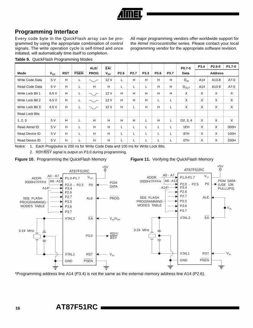
Programming InterfaceEvery code byte in the QuickFlash array can be pro-grammed by using the appropriate combination of controlsignals. The write operation cycle is self-timed and onceinitiated, will automatically time itself to completion.
All major programming vendors offer worldwide support forthe Atmel microcontroller series. Please contact your localprogramming vendor for the appropriate software revision.
Notes: 1. Each Prog/pulse is 200 ns for Write Code Data and 100 ms for Write Lock Bits.
2. RDY/BSY signal is output on P3.0 during programming.
Figure 10. Programming the QuickFlash Memory Figure 11. Verifying the QuickFlash Memory
*Programming address line A14 (P3.4) is not the same as the external memory address line A14 (P2.6).
Table 9. QuickFlash Programming Modes
Mode VCC RST PSEN
ALE/
PROG
EA/
VPP P2.6 P2.7 P3.3 P3.6 P3.7
P0.7-0
Data
P3.4 P2.5-0 P1.7-0
Address
Write Code Data 5 V H L 12 V L H H H H DIN A14 A13-8 A7-0
Read Code Data 5 V H L H H L L L H H DOUT A14 A13-8 A7-0
Write Lock Bit 1 6.5 V H L 12 V H H H H H X X X X
Write Lock Bit 2 6.5 V H L 12 V H H H L L X X X X
Write Lock Bit 3 6.5 V H L 12 V H L H H L X X X X
Read Lock Bits
1, 2, 3 5 V H L H H H H L H L D2, 3, 4 X X X
Read Atmel ID 5 V H L H H L L L L L 1EH X X 000H
Read Device ID 5 V H L H H L L L L L 87H X X 100H
Read Device ID 5 V H L H H L L L L L 07H X X 200H
P1.0-P1.7
P2.6
P3.6
P2.0 - P2.5
A0 - A7ADDR.
0000H/7FFFH
SEE FLASHPROGRAMMINGMODES TABLE
3-24 MHz
A14*P0
+5V
P2.7
PGMDATA
PROG
V /VIH PP
VIH
ALE
P3.7
XTAL2 EA
RST
PSEN
XTAL1
GND
VCC
AT87F51RC
P3.4
P3.3
P3.0RDY/BSY
A8 - A13P1.0-P1.7
P2.6
P3.6
P2.0 - P2.5
A0 - A7ADDR.
0000H/7FFFH
SEE FLASHPROGRAMMINGMODES TABLE
3-24 MHz
P0
+5V
P2.7
PGM DATA(USE 10KPULLUPS)
VIH
VIH
ALE
P3.7
XTAL2 EA
RST
PSEN
XTAL1
GND
VCC
A14*
AT87F51RC
P3.4
P3.3
A8 - A13
AT87F51RC16

AT87F51RC
QuickFlash Programming and Verification Waveforms
QuickFlash Programming and Verification CharacteristicsTA = 0°C to 70°C, VCC = 5.0 ± 10%
Symbol Parameter Min Max Units
VPP Programming Supply Voltage 11.5 12.0 V
IPP Programming Supply Current 10 mA
ICC VCC Supply Current 30 mA
1/tCLCL Oscillator Frequency 3 24 MHz
tAVGL Address Setup to PROG Low 48tCLCL
tGHAX Address Hold after PROG 48tCLCL
tDVGL Data Setup to PROG Low 48tCLCL
tGHDX Data Hold after PROG 48tCLCL
tEHSH P2.7 (ENABLE) High to VPP 48tCLCL
tSHGL VPP Setup to PROG Low 10 µs
tGHSL VPP Hold after PROG 10 µs
tGLGH PROG Width 0.2 1 µs
tAVQV Address to Data Valid 48tCLCL
tELQV ENABLE Low to Data Valid 48tCLCL
tEHQZ Data Float after ENABLE 0 48tCLCL
tGHBL PROG High to BUSY Low 1.0 µs
tWC Byte Write Cycle Time 80 µs
tGLGHtGHSL
tAVGL
tSHGL
tDVGLtGHAX
tAVQV
tGHDX
tEHSH tELQV
tWC
BUSY READY
tGHBL
tEHQZ
P1.0 - P1.7P2.0 - P2.5
P3.4
ALE/PROG
PORT 0
LOGIC 1LOGIC 0EA/VPP
VPP
P2.7(ENABLE)
P3.0(RDY/BSY)
PROGRAMMINGADDRESS
VERIFICATIONADDRESS
DATA IN DATA OUT
17

Notes: 1. Under steady state (non-transient) conditions, IOL must be externally limited as follows:Maximum IOL per port pin: 10 mAMaximum IOL per 8-bit port:Port 0: 26 mA Ports 1, 2, 3: 15 mAMaximum total IOL for all output pins: 71 mAIf IOL exceeds the test condition, VOL may exceed the related specification. Pins are not guaranteed to sink current greater than the listed test conditions.
2. Minimum VCC for Power-down is 2V.
Absolute Maximum Ratings*Operating Temperature.................................. -55°C to +125°C *NOTICE: Stresses beyond those listed under “Absolute
Maximum Ratings” may cause permanent dam-age to the device. This is a stress rating only and functional operation of the device at these or any other conditions beyond those indicated in the operational sections of this specification is not implied. Exposure to absolute maximum rating conditions for extended periods may affect device reliability.
Storage Temperature ..................................... -65°C to +150°C
Voltage on Any Pinwith Respect to Ground .....................................-1.0V to +7.0V
Maximum Operating Voltage ............................................ 6.6V
DC Output Current...................................................... 15.0 mA
DC CharacteristicsThe values shown in this table are valid for TA = -40°C to 85°C and VCC = 5.0V ± 20%, unless otherwise noted.
Symbol Parameter Condition Min Max Units
VIL Input Low-voltage (Except EA) -0.5 0.2 VCC-0.1 V
VIL1 Input Low-voltage (EA) -0.5 0.2 VCC-0.3 V
VIH Input High-voltage (Except XTAL1, RST) 0.2 VCC+0.9 VCC+0.5 V
VIH1 Input High-voltage (XTAL1, RST) 0.7 VCC VCC+0.5 V
VOL Output Low-voltage(1) (Ports 1,2,3) IOL = 1.6 mA 0.45 V
VOL1Output Low-voltage(1)
(Port 0, ALE, PSEN)IOL = 3.2 mA 0.45 V
VOHOutput High-voltage(Ports 1,2,3, ALE, PSEN)
IOH = -60 µA, VCC = 5V ± 10% 2.4 V
IOH = -25 µA 0.75 VCC V
IOH = -10 µA 0.9 VCC V
VOH1Output High-voltage(Port 0 in External Bus Mode)
IOH = -800 µA, VCC = 5V ± 10% 2.4 V
IOH = -300 µA 0.75 VCC V
IOH = -80 µA 0.9 VCC V
IIL Logical 0 Input Current (Ports 1,2,3) VIN = 0.45V -50 µA
ITLLogical 1 to 0 Transition Current (Ports 1,2,3)
VIN = 2V, VCC = 5V ± 10% -650 µA
ILI Input Leakage Current (Port 0, EA) 0.45 < VIN < VCC ±10 µA
RRST Reset Pull-down Resistor 50 300 KΩ
CIO Pin Capacitance Test Freq. = 1 MHz, TA = 25°C 10 pF
ICC
Power Supply CurrentActive Mode, 12 MHz 25 mA
Idle Mode, 12 MHz 6.5 mA
Power-down Mode(1)VCC = 6V 100 µA
VCC = 3V 40 µA
AT87F51RC18

AT87F51RC
AC Characteristics Under operating conditions, load capacitance for Port 0, ALE/PROG, and PSEN = 100 pF; load capacitance for all otheroutputs = 80 pF.
External Program and Data Memory Characteristics
Symbol Parameter
12 MHz Oscillator Variable Oscillator
UnitsMin Max Min Max
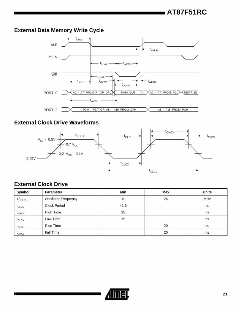
1/tCLCL Oscillator Frequency 0 24 MHz
tLHLL ALE Pulse Width 127 2tCLCL-40 ns
tAVLL Address Valid to ALE Low 43 tCLCL-13 ns
tLLAX Address Hold after ALE Low 48 tCLCL-20 ns
tLLIV ALE Low to Valid Instruction In 233 4tCLCL-65 ns
tLLPL ALE Low to PSEN Low 43 tCLCL-13 ns
tPLPH PSEN Pulse Width 205 3tCLCL-20 ns
tPLIV PSEN Low to Valid Instruction In 145 3tCLCL-45 ns
tPXIX Input Instruction Hold after PSEN 0 0 ns
tPXIZ Input Instruction Float after PSEN 59 tCLCL-10 ns
tPXAV PSEN to Address Valid 75 tCLCL-8 ns
tAVIV Address to Valid Instruction In 312 5tCLCL-55 ns
tPLAZ PSEN Low to Address Float 10 10 ns
tRLRH RD Pulse Width 400 6tCLCL-100 ns
tWLWH WR Pulse Width 400 6tCLCL-100 ns
tRLDV RD Low to Valid Data In 252 5tCLCL-90 ns
tRHDX Data Hold after RD 0 0 ns
tRHDZ Data Float after RD 97 2tCLCL-28 ns
tLLDV ALE Low to Valid Data In 517 8tCLCL-150 ns
tAVDV Address to Valid Data In 585 9tCLCL-165 ns
tLLWL ALE Low to RD or WR Low 200 300 3tCLCL-50 3tCLCL+50 ns
tAVWL Address to RD or WR Low 203 4tCLCL-75 ns
tQVWX Data Valid to WR Transition 23 tCLCL-20 ns
tQVWH Data Valid to WR High 433 7tCLCL-120 ns
tWHQX Data Hold after WR 33 tCLCL-20 ns
tRLAZ RD Low to Address Float 0 0 ns
tWHLH RD or WR High to ALE High 43 123 tCLCL-20 tCLCL+25 ns
19

External Program Memory Read Cycle
External Data Memory Read Cycle
tLHLL
tLLIV
tPLIV
tLLAXtPXIZ
tPLPH
tPLAZtPXAV
tAVLL tLLPL
tAVIV
tPXIX
ALE
PSEN
PORT 0
PORT 2 A8 - A15
A0 - A7 A0 - A7
A8 - A15
INSTR IN
tLHLL
tLLDV
tLLWL
tLLAX
tWHLH
tAVLL
tRLRH
tAVDV
tAVWL
tRLAZ tRHDX
tRLDV tRHDZ
A0 - A7 FROM RI OR DPL
ALE
PSEN
RD
PORT 0
PORT 2 P2.0 - P2.7 OR A8 - A15 FROM DPH
A0 - A7 FROM PCL
A8 - A15 FROM PCH
DATA IN INSTR IN
AT87F51RC20
AT87F51RC
External Data Memory Write Cycle
External Clock Drive Waveforms
tLHLL
tLLWL
tLLAX
tWHLH
tAVLL
tWLWH
tAVWL
tQVWXtQVWH
tWHQX
A0 - A7 FROM RI OR DPL
ALE
PSEN
WR
PORT 0
PORT 2 P2.0 - P2.7 OR A8 - A15 FROM DPH
A0 - A7 FROM PCL
A8 - A15 FROM PCH
DATA OUT INSTR IN
tCHCX
tCHCX
tCLCX
tCLCL
tCHCLtCLCHV - 0.5VCC
0.45V0.2 V - 0.1VCC
0.7 VCC
External Clock DriveSymbol Parameter Min Max Units
1/tCLCL Oscillator Frequency 0 24 MHz
tCLCL Clock Period 41.6 ns
tCHCX High Time 15 ns
tCLCX Low Time 15 ns
tCLCH Rise Time 20 ns
tCHCL Fall Time 20 ns
21

Shift Register Mode Timing Waveforms
AC Testing Input/Output Waveforms(1)
Note: 1. AC Inputs during testing are driven at VCC - 0.5V for a logic 1 and 0.45V for a logic 0. Timing mea-surements are made at VIH min. for a logic 1 and VIL max. for a logic 0.
Float Waveforms(1)
Note: 1. For timing purposes, a port pin is no longer floating when a 100 mV change from load voltage occurs. A port pin begins to float when a 100 mV change from the loaded VOH/VOL level occurs.
Serial Port Timing: Shift Register Mode Test ConditionsThe values in this table are valid for VCC = 5.0V ± 20% and Load Capacitance = 80 pF.
Symbol Parameter
12 MHz Osc Variable Oscillator
UnitsMin Max Min Max
tXLXL Serial Port Clock Cycle Time 1.0 12tCLCL µs
tQVXH Output Data Setup to Clock Rising Edge 700 10tCLCL-133 ns
tXHQX Output Data Hold after Clock Rising Edge 50 2tCLCL-117 ns
tXHDX Input Data Hold after Clock Rising Edge 0 0 ns
tXHDV Clock Rising Edge to Input Data Valid 700 10tCLCL-133 ns
tXHDV
tQVXH
tXLXL
tXHDX
tXHQX
ALE
INPUT DATA
CLEAR RI
OUTPUT DATA
WRITE TO SBUF
INSTRUCTION
CLOCK
0
0
1
1
2
2
3
3
4
4
5
5
6
6
7
7
SET TI
SET RI
8
VALID VALIDVALID VALIDVALID VALIDVALID VALID
0.45V
TEST POINTS
V - 0.5VCC 0.2 V + 0.9VCC
0.2 V - 0.1VCC
VLOAD+ 0.1V
Timing ReferencePoints
V
LOAD- 0.1V
LOAD
V VOL+ 0.1V
VOL- 0.1V
AT87F51RC22

AT87F51RC
Ordering InformationSpeed(MHz)
PowerSupply Ordering Code Package Operation Range
12 5V ± 20% AT87F51RC-12ACAT87F51RC-12JC
AT87F51RC-12PC
44A44J
40P6
Commercial(0° C to 70° C)
AT87F51RC-12AIAT87F51RC-12JIAT87F51RC-12PI
44A44J40P6
Industrial(-40° C to 85° C)
16 5V ± 20% AT87F51RC-16AC
AT87F51RC-16JCAT87F51RC-16PC
44A
44J40P6
Commercial
(0° C to 70° C)
AT87F51RC-16AIAT87F51RC-16JI
AT87F51RC-16PI
44A44J
40P6
Industrial(-40° C to 85° C)
20 5V ± 20% AT87F51RC-20ACAT87F51RC-20JCAT87F51RC-20PC
44A44J40P6
Commercial(0° C to 70° C)
AT87F51RC-20AI
AT87F51RC-20JIAT87F51RC-20PI
44A
44J44Q
Industrial
(-40° C to 85° C)
24 5V ± 20% AT87F51RC-24ACAT87F51RC-24JC
AT87F51RC-24PC
44A44J
40P6
Commercial(0° C to 70° C)
AT87F51RC-24AIAT87F51RC-24JIAT87F51RC-24PI
44A44J40P6
Industrial(-40° C to 85° C)
23
Package Type
44A 44-lead, Thin Plastic Gull Wing Quad Flatpack (TQFP)
44J 44-lead, Plastic J-Leaded Chip Carrier (PLCC)
40P6 40-lead, 0.600" Wide, Plastic Dual Inline Package (PDIP)

Packaging Information
*Controlling dimension: millimeters
1.20(0.047) MAX
10.10(0.394)9.90(0.386)
SQ
12.21(0.478)11.75(0.458)
SQ
0.75(0.030)0.45(0.018)
0.15(0.006)0.05(0.002)
0.20(.008)0.09(.003)
07
0.80(0.031) BSC
PIN 1 ID
0.45(0.018)0.30(0.012)
AT87F51RC24
.045(1.14) X 45° PIN NO. 1IDENTIFY
.045(1.14) X 30° - 45° .012(.305).008(.203)
.021(.533)
.013(.330)
.630(16.0)
.590(15.0)
.043(1.09)
.020(.508)
.120(3.05)
.090(2.29).180(4.57).165(4.19)
.500(12.7) REF SQ
.032(.813)
.026(.660)
.050(1.27) TYP
.022(.559) X 45° MAX (3X)
.656(16.7)
.650(16.5)
.695(17.7)
.685(17.4)SQ
SQ
2.07(52.6)2.04(51.8) PIN
1
.566(14.4)
.530(13.5)
.090(2.29)MAX
.005(.127)MIN
.065(1.65)
.015(.381)
.022(.559)
.014(.356).065(1.65).041(1.04)
015
REF
.690(17.5)
.610(15.5)
.630(16.0)
.590(15.0)
.012(.305)
.008(.203)
.110(2.79)
.090(2.29)
.161(4.09)
.125(3.18)
SEATINGPLANE
.220(5.59)MAX
1.900(48.26) REF
JEDEC STANDARD MS-011 AC
44A, 44-lead, Thin (1.0 mm) Plastic Gull Wing Quad Flat Package (TQFP)Dimensions in Millimeters and (Inches)*
44J, 44-lead, Plastic J-Leaded Chip Carrier (PLCC)Dimensions in Inches and (Millimeters)
40P6, 40-lead, 0.600" Wide, Plastic Dual Inline Package (PDIP)Dimensions in Inches and (Millimeters)

© Atmel Corporation 1998.Atmel Corporation makes no warranty for the use of its products, other than those expressly contained in the Company’s standard war-ranty which is detailed in Atmel’s Terms and Conditions located on the Company’s web site. The Company assumes no responsibility forany errors which may appear in this document, reserves the right to change devices or specifications detailed herein at any time withoutnotice, and does not make any commitment to update the information contained herein. No licenses to patents or other intellectual prop-erty of Atmel are granted by the Company in connection with the sale of Atmel products, expressly or by implication. Atmel’s products arenot authorized for use as critical components in life support devices or systems.
Atmel Headquarters Atmel Operations
Corporate Headquarters2325 Orchard ParkwaySan Jose, CA 95131TEL (408) 441-0311FAX (408) 487-2600
EuropeAtmel U.K., Ltd.Coliseum Business CentreRiverside WayCamberley, Surrey GU15 3YLEnglandTEL (44) 1276-686677FAX (44) 1276-686697
AsiaAtmel Asia, Ltd.Room 1219Chinachem Golden Plaza77 Mody RoadTsimshatsui EastKowloon, Hong KongTEL (852) 27219778FAX (852) 27221369
JapanAtmel Japan K.K.Tonetsu Shinkawa Bldg., 9F1-24-8 ShinkawaChuo-ku, Tokyo 104-0033JapanTEL (81) 3-3523-3551FAX (81) 3-3523-7581
Atmel Colorado Springs1150 E. Cheyenne Mtn. Blvd.Colorado Springs, CO 80906TEL (719) 576-3300FAX (719) 540-1759
Atmel RoussetZone Industrielle13106 Rousset Cedex, FranceTEL (33) 4 42 53 60 00FAX (33) 4 42 53 60 01
Fax-on-DemandNorth America:1-(800) 292-8635
International:1-(408) 441-0732
Web Sitehttp://www.atmel.com
BBS1-(408) 436-4309
Printed on recycled paper.
1106C–02/00/xM
Marks bearing ® and/or ™ are registered trademarks and trademarks of Atmel Corporation.
Terms and product names in this document may be trademarks of others.