
PDF (1.25 MB) - IOPscience
13
Journal of Physics: Conference Series OPEN ACCESS Dimensional measurement of 3D microstruture based on white light interferometer To cite this article: S C H Thian et al 2007 J. Phys.: Conf. Ser. 48 265 View the article online for updates and enhancements. You may also like Proper orthogonal decomposition and component mode synthesis in macromodel generation for the dynamic simulation of a complex MEMS device W Z Lin, K H Lee, S P Lim et al. - Rhombohedral and tetragonal nanotwin domains and thermally induced phase transformations in PZN–8%PT single crystals W S Chang, L C Lim, P Yang et al. - Structural phase transformations and nanotwin domains in 0.93Pb(Zn 1/3 Nb 2/3 )O 3 –0.07PbTiO 3 W S Chang, L C Lim, P Yang et al. - Recent citations Rapid characterization of nano-scale structures in large-scale ultra-precision surfaces Wenjun Yang et al - Surface Profile Measurement and Error Compensation of Triangular Microstructures Employing a Stylus Scanning System Qin Yin et al - Performance verification of a photogrammetric scanning system for micro-parts using a three-dimensional artifact: adjustment and calibration F. Lavecchia et al - This content was downloaded from IP address 187.95.60.227 on 23/12/2021 at 03:04
Transcript of PDF (1.25 MB) - IOPscience

Journal of Physics Conference Series
OPEN ACCESS
Dimensional measurement of 3D microstruturebased on white light interferometerTo cite this article S C H Thian et al 2007 J Phys Conf Ser 48 265
View the article online for updates and enhancements
You may also likeProper orthogonal decomposition andcomponent mode synthesis in macromodelgeneration for the dynamic simulation of acomplex MEMS deviceW Z Lin K H Lee S P Lim et al
-
Rhombohedral and tetragonal nanotwindomains and thermally induced phasetransformations in PZNndash8PT singlecrystalsW S Chang L C Lim P Yang et al
-
Structural phase transformationsand nanotwin domains in093Pb(Zn13Nb23)O3ndash007PbTiO3W S Chang L C Lim P Yang et al
-
Recent citationsRapid characterization of nano-scalestructures in large-scale ultra-precisionsurfacesWenjun Yang et al
-
Surface Profile Measurement and ErrorCompensation of TriangularMicrostructures Employing a StylusScanning SystemQin Yin et al
-
Performance verification of aphotogrammetric scanning system formicro-parts using a three-dimensionalartifact adjustment and calibrationF Lavecchia et al
-
This content was downloaded from IP address 1879560227 on 23122021 at 0304
Dimensional measurement of 3D microstruture based on white light interferometer
S C H Thian W Feng Y S Wong J Y H Fuh H T Loh K H Tee Y Tang and L Lu
Mechanical Engineering Department National University of Singapore 9 Engineering Drive 1 Singapore 117576
mpetchsnusedusg mpefengwnusedusg mpewysnusedusg mpefuhyhnusedusg mpelhtnusedusg u0204753nusedusg mpetyxnusedusg mpelulinusedusg
Abstract Dimensional metrology for micronano structure is crucial for addressing quality issues and understanding the performance of micro-fabricated products and micro-fabrication processes Most of the established methods are based on optical microscopy for planar dimensions and stylus profilometry for out-of-plane dimensions Contact profilers suffer from slow speed of measurement for three-dimensional profiles and are not suitable for delicate surfaces and parts Advanced systems using white light interferometer are equipped with CCD cameras and interfaced with a microscope to conduct an array of measurements ranging from two-dimensional to three-dimensional profiles and surface roughness analysis This paper presents a methodology based on white light interferometer for the dimensional measurement of 3D micro-structures demonstrated on micro-gears and moulds produced by UV lithography and vacuum casting respectively Physical artifacts such as gauge blocks are also utilized to verify and validate the measurements on the microcomponents
Keywords methodology microcomponents metrology surface roughness white light interferometer
Submit to Measurement Science and Technology
IOP Publishing Journal of Physics Conference Series 48 (2006) 1435ndash101doi1010881742-6596481265 International Symposium on Instrumentation Science and Technology
1435copy 2006 IOP Publishing Ltd
1 Introduction Many of the Micro-Electro-Mechanical-System (MEMS) processes developed from lithography-based microfabrication and micromachining techniques are commonly derived from the microelectronics industry and offer the potential of great cost reduction in batch fabrication processes for high-volume manufacturing [1]
To minimize errors a metrology system for MEMS must have sub-micron precision sub-millisecond sensing and reliable and robust performance in harsh environment and miniaturized hardware that can be easily integrated into existing systems [2] It is crucial for addressing quality issues of micromanufactured products and processes The quality issues may be divided into two equally important phases RampD and production From an RampD perspective metrology is essential for understanding the performance of newly developed products and processes From a production standpoint metrology is necessary to ensure that the products are fabricated correctly In due course the assurance of producing products that are in specification requires that the production process be controlled
In micromanufacturing dimensional metrology it is interesting to note that many of the inspections are still accomplished by optical microscopes or scanning electron microscopes (SEM) although SEM does not reflect accurate 3D dimensions and style contact profiler is not suitable for delicate surfaces may be damaged by the stylus Most published results and measurements are based on SEM with few from the white light interferometery (WLI) In view of these the main metrology equipment used in this paper as benchmark and comparison would be WLI systems which are the Veeco WYKOreg NT1100 [3] and the Zygo NewView 5000TM [4]
Optical profilers also known as WLI appears to be the leading metrology equipment for small 3D objects as WLI can image for 3D metrology based on interferometric measurements Other qualities include high-speed data acquisition wide measurement area large vertical range and sub-nanometer vertical resolution as well as the ability to measure 3D profiles in one measurement where in usual engineering surfaces the measurement field should cover an area of several square millimeters [5] This unique set of strengths supports a variety of metrology applications in RampD product and process development manufacturing and quality control Various 3D metrology techniques can be summarized in two categories contact and non-contact
11 Contact Method Conventional contact measurement in 3D surface profiling and roughness measurements has been a reliable method for hard sample surfaces and the contact methods are insensitive to optical properties of the surface such as transparency
The 4 common contact types of equipment are Contact Stylus Profiler Coordinate Measurement Machine (CMM) and Scanning Probe Microscopes (SPM)
111 Contact Stylus Profiler It is widely used to monitor chemical mechanical planarization (CMP) performance in electronics fabrication [6] and are typically used to measure step heights long-range planarity and long-range variations in local surface roughness in a single scan usually Inevitably the limits of the amplitude which can be measured and the limits on spatial wavelengths are restricted by the physical dimension of the stylus tip and its angle [7] In addition stylus profilers can measure step heights on vertical and near-vertical steps taller than those possible with the AFM such as a silicon micro-probe with a sharp tip used to measure the inner profile of high aspect-ratio microstructures [8]
112 Coordinate Measuring Machine (CMM) CMMs have revolutionized the dimensional metrology of virtually all types of manufactured components not only for their accuracy convenience and simplicity of operation but also because of the wide range of industries covering a broad array of applications [9] With several measuring sensors integrated with the equipment such as optical sensor it is capable to perform the same function as the microscope-based inspection systems contact tactile
1436
measurement head similar to that of contact stylus probe and a vision system that is used to aid in the positioning of the tactile probe [5] Takaya et al [10]-[11] developed a laser trapping probe for nano-CMM It can achieve a possible resolution of 10 nm and has a measuring force of 001mN which makes it possible to achieve nanometer sensitivity comparable to the AFM 113 Scanning Probe Microscopes (SPM) The big difference between SPM and the conventional stylus is that they rely for their signal on quantum-mechanical effects such as tunneling current for STM AFM and STM can measure deflections that are much less than 1 angstrom (Aring) Hence they are the most common method used for surface roughness measurement in the nano scale
The major advantage of these new-generation microscopes is their ability to measure more than one feature In STM by varying the voltage between the specimen and the probe tip the instrument can be used as a topographer and spectroscope widely used in the measurement and detection of growth in biological specimen the machining of substrates and the microfabrication
By utilizing this basic technique in STM to detect deflection in AFM cantilevers other varied techniques [12] evolved such as magnetic force microscopy (MFM) where the probe is magnetized electrostatic microscopy (EFM) where the probe has an electrostatic charge scanning thermal microscopy (SThM) where the probe acts as a thermocouple and near-field scanning optical microscopy (NSOM) where the probe is in fact a sub-micrometer aperture [13]
12 Non-contact method Non-contact measurement is of significant interest because it avoids deformation of the products and mechanical errors in the contact measurement Hence they are suitable for very delicate machined surfaces The basic principle of an active non-contact range finding system is to project a radio-wave ultrasonic or optical source onto an object and process the reflected signal to determine its range
The 4 common types of non-contact equipment are Confocal Scanning Optical Microscope (CSOM) White Light Interferometry (WLI) Scanning Electron Microscope (SEM) and Tunneling Electron Microscope (TEM)
121 Confocal Scanning Optical Microscope (CSOM) CSOM is primarily used to measure the topography of biological tissues and 2-D profiles [14] but has been introduced for 3-D measurement through reconstruction of a volume of the specimen and assembling a series of thin slices taken along the vertical axis [15] Udupa et al [16]-[17] applied CSOM to micro and macro surface irregularities and concluded that it was a useful tool for this purpose
122 White Light Interferometry (WLI) Interferometry is popular for surface profiling Generally this mode utilizes the coherent property of the light the interference between the light and that scattered from the test surface and from a reference surface such as a glass flat surface to produce fringes The fringe contours can then be examined through the contour pattern when viewed to derive a very clear picture of the general surface geometry If the fringes are sharpened up by means of multiple-beam interferometry the surface roughness can be measured Furthermore WLI does not involve phase shifting or complex algorithms and is theoretically unlimited in the vertical scan length which is only constrained by how far the reference mirror can move
The drawbacks of an interferometer are that it cannot read discontinuities of the object geometry as in the case of sharp edges and only works in relative coordinate space These sharp edges can produce misleading diffraction spikes which can be mistaken for real peaks and thus can be a major problem in calibration
123 Scanning Electron Microscope (SEM) SEM is the most common equipment being used to illustrate scale of the microstructures but the drawbacks of SEM are the distortion produced by sharp edges curvatures and slopes in the object which are qualitative in nature making calibration a problem Inevitably SEM is widely utilized in imaging rather than for metrology
1437
124 Tunneling Electron Microscope (TEM) TEM is generally well suited to thin samples where higher order of electron energy than SEM is used Moreover a high energy source means a smaller de Broglie wavelength and this implies a smaller feature or simply higher resolution up to atomic (angstrom)-level than SEM However TEM is not as important in surface metrology because most engineering surfaces are opaque and since the energy beam is traveling through the sample the sample bulk and not the surface is being imaged
Table 1 List some typical values for the instruments mentioned
Resolution Range Equipment Mode Lateral Vertical Vertical
Stylus Contact 01 μm 03nm 50μm
CMM Contact 10 μm 10 nm 10 mm
AFM Contact 05 nm 005 nm 6μm
STM Contact 25 nm 02 nm 100 nm
Confocal
Microscope Non contact 1 μm 01 μm 50 mm
WLI Non contact 045μm 01 nm 5 mm
SEM Non contact 10 nm 2 nm 2μm
TEM Non contact 2 nm to 1μm 2μm 100 nm
2 White Light Interferometery (WLI)
Figure 1 Basic configuration of white light scanning interferometry
Typically in an interferometer a beam of white light or monochromatic light source splits into two separate beams and is then recombined The resulting interference occurrence is subsequently recorded in the form of an interferogram [18] which is a discrete fringe pattern and is processed by
1438
the computer for data measurement and analysis using various phase mapping techniques such as phase-shifting interferometry (PSI) and vertical scanning interferometry (VSI) Data analysis of the sample such as average roughness peak-to-valley height 2D and 3D false-color height maps histograms bearing ratio curvature and volume analysis etc are eventually possible depending on the software applied Figure 1 shows a typical set up of the scanning interferometry of WLI
21 Principle of Operation Using the Veeco WYKO NT 1100 as an example the working principle of a WLI shown in figure 2 can be illustrated in the following steps
Figure 2 Typical microscope based white light interferometer
White light from the illuminator generated by a halogen lamp travels through the aperture stop
and field stop The aperture stop controls the focusing of the light while the field stop controls the field-of-view (FOV) on the charged-coupled-device (CCD) camera
Bypassing the field and aperture stop the light is reflected down to the interferometer (interfaced with a translator reference mirror and a microscope objective) by a beam splitter
Once the light reaches the objective another beam splitter separates the light into two beams One beam the reference beam reflects from a super smooth reference mirror inside the objective while the other (the test beam) reflects from the surface of the sample and back to the objective
If the surface of the sample is in focus as shown in figure 3 the two light beams will recombine to create bright and dark bands called ldquofringesrdquo that make up the interferogram Fringes like lines on a topographic map represent the topography of the object and can be used to gauge the surface roughness of the sample object The number of fringes and their spacing depend on the relative tilt between the sample and the reference mirror
Subsequently during the scanning the reference surface is translated relative to the test sample by the translator such that every point on the surface passes through the focus Throughout the scan a series of intensity of data frames which are shown as interferograms is recorded by the CCD detector and the data frame is forwarded to the computer for processing
Finally these frames are analyzed using various interferometric phase mapping programs such PSI for surfaces below 160nm and VSI for surfaces above 160nm [19] to determine the height of each point on the surface Using these data it is now possible to analyze the sample in details using appropriate software
1439
Figure 3 Images of interference fringe patterns (interferogram)
3 Metrology Samples and Equipments Prior to any part geometry validation it is crucial that the readings and measurements obtained from the measuring instrument are accurate and precise Hence it is necessary to conduct a preliminary analysis using metrology sample of calibrated dimensions to check the equipment accuracy and precision
To compare the limitation andor capability of the equipment a master micro-gear created by UV lithography and a cast micro-gear and micro moulds made by vacuum casting are measured and analyzed
31 Metrology Samples and Gage Blocks Several 1mm diameter micro-gear and micro-moulds samples (figure 4) together with the other test components of known dimensions which are the photo mask (figure 5) and gauge blocks are utilized to assess the capabilities and limitations of the metrology equipment based on benchmarking and performance measures with respect to various metrology criteria and principles
Gauge blocks are defined internationally by ISO specification [20] with flat and parallel opposing surfaces and are high-precision calibrated artifacts of known dimensions used as calibration gages in equipment performance validation and dimensional calibration A Grade 00 gauge block certified by ISO Standard 3650 is used for step height analysis while a photo mask (figure 5) is used for lateral comparison of geometric dimensions
(a) (b) (c) Figure 4 Micro-gear samples (a) Silicon micro-mould (b) Cast wax micro-gear (c) cast polyurethane (PU) micro-gear
Figure 5 Photo mask for photolithography
32 Metrology Aspects and Features of the Samples A set of measurements is defined to describe the micro-gear or micro-gear cavity shown in figure 6 and figure 7
Focused clear image (with fringes present)
Out of focus (without fringes present)
1440
For micro-gears made of SU-8 (by UV lithography) wax and polyurethane (by casting) the gear diameter hub diameter hub width gear height and surface roughness of the gear top surface are selected for this purpose For micro-gear cavities in the silicone rubber moulds similar features are measured
The difference between the gear pattern and cavity metrology features in the selected surfaces lies in the fact that the top surface of the gear is copied onto the mould as the bottom surface of the cavity
In addition the photo mask shares the same measurement features but the surface roughness and thickness are not considered
Figure 6 Out-of-plane surface metrology
Figure 7 In- plane lateral measurements
4 Results and Discussion
41 Gauge Block Analysis The measurements selected for gage block 5 10 20 30 and 40 μm each repeated 15 times Table 2 below shows the summarized tabulated results
Table 2 Results of 16 measurements for each of several Gage block step heights
Gage Block Thickness Metrology Equipment
5 μm 10 μm 20 μm 30 μm 40 μm
Veeco optical profiler
(5X Michelson
Objective)
5007 μm
plusmn 418 nm
10214 μm
plusmn 432 nm
20002 μm
plusmn 558 nm
30178 μm
plusmn 153 nm
40253 μm
plusmn 162 nm
Zygo optical profiler
(5X Michelson
Objective)
5529 μm
plusmn 316 nm
10260 μm
plusmn 342 nm
20254 μm
plusmn 444 nm
30247 μm
plusmn 428 nm
40214 μm
plusmn 226 nm
Height Surface
2X
1441
Talysurf -120 stylus
profiler
(tip radius 2μm)
5334 μm
plusmn 182 nm
10293 μm
plusmn 366 nm
20335 μm
plusmn 508 nm
30331 μm
plusmn 554 nm
40357 μm
plusmn 674 nm
Keyence digital
microscope
(450X objective)
501 μm
plusmn 1464 nm
1019 μm
plusmn 2828 nm
2019 μm
plusmn 3346 nm
3044 μm
plusmn 3574 nm
4037 μm
plusmn 3100 nm
Mahr OMS-400 CMM
(non-contact laser probe)
6 μm
plusmn 3492 nm
10 μm
plusmn 1962 nm
21 μm
plusmn 1500 nm
27 μm
plusmn 1438 nm
37 μm
plusmn 1544 nm
From table 2 it can be observed that both white light optical profiler and contact stylus have a standard deviation of less than 70nm or 007 μm as compared to the Keyence digital microscope and CMM laser probe of standard deviation greater than 1400nm up to 3000nm at 95 coverage
42 Micro-gear Samples Analysis The gear diameter (outer and inner) hub diameter hub width gear height and surface roughness of the gear top surface are measured by the equipment and compared accordingly Figure 8 shows a sample of the results taken from WLI (Veeco and Zygo optical profiler) CMM SEM and optical microscope respectively
(a) (b)
(c) (d)
(e) (f)
1442
Figure 8 Outer diameter measured by (a) Veeco and (b) Zygo optical profiler (c) CMM (d) SEM (e) Keyence digital microscope (f) Leica digital microscope
The outer diameter measured by both WLI are generated by the software (figure 8(a) 8(b) 8(e)
and 8f) while simple subtraction is need for CMM (figure 8(c)) The results clearly show that SEM could not give accurate dimension reading
The outer diameter for both the microgears and micro-cavities is defined as the average tooth-to-tooth distance of two oppositely-facing gear teeth As shown in figure 8(e) and 8(f) there are eight possible orientations by which the tooth-to-tooth distance can be measured Measurements were taken from these eight orientations to account for any non-uniformity or roundness in the gear The measurement at each orientation was repeated to reduce the operatorrsquos error and the error imposed by the equipment tolerance
43 Photo mask Analysis By using a photo mask for UV photolithography it is possible to validate the accuracy of the lateral pixel density assigned by the metrology equipment and also to verify the photo mask gear features Only selected equipment is used for analysis due to limitation to hold the photo mask Results of the analysis are illustrated in table 3 below
Table 3 Results for Photo mask analysis
Photo mask
Diameter
Metrology Equipment
Hub Width 100 μm
Outer 1000 μm
Inner 360 μm
Veeco Optical Profiler - 5X Michelson for diameter analysis - 50X Mirau for hub width analysis
9980 plusmn 0566 μm
99781 plusmn 196 μm
35944 plusmn 193 μm
Zygo Optical Profiler - 5X Michelson for diameter analysis - 50X Mirau for hub width analysis
10057 plusmn 169 μm
99800 plusmn 310 μm
35894 plusmn 322 μm
Leica Digital Microscope - 5X for outer diameter analysis - 20X for inner diameter and hub width analysis
9976 plusmn 0892 μm
99919 plusmn 156 μm
35960 plusmn 122 μm
Keyence Digital Microscope - 175X for outer diameter analysis - 450X for inner diameter and hub width analysis
10067 plusmn 0752 μm
105499 plusmn 140 μm
37167 plusmn 1185 μm
44 Surface Roughness Analysis Surface roughness is typically measured by AFM and contact profiler Here we compared the surface roughness of a PU microgear measured by 3 different types of equipments Table 4 summaries the results
2X
1443
Table 4 Surface roughness of PU microgear
Metrology Equipment Average Surface Roughness Ra (nm) of PU micro-gear
Optical Profiler (Veeco WKYO NT1100)
2053 plusmn 252
Optical Profiler (Zygo NewView 5000)
2685 plusmn 125
CMM (Mahr OMS-400 CMM)
NA
SEM (Jeol JSM-5500 SEM)
NA
Digital Microscope (Keyence VHX-100)
NA
Digital Microscope (Leica DC 300)
NA
Contact Profiler (Talysurf -120 stylus Profiler)
1164 plusmn 229
AFM (SPA-500 AFM)
785 plusmn 046
From the average roughness Ra Zygo optical profiler (2685nm) Veeco optical profiler (2053nm) Talysurf profiler (1164nm) and AFM (785nm) this serves to affirm the deduction regarding stylus which reduces the signal-to-noise ratio while the optics appears to increase the noise described by Whitehouse et al [21]
Contact profiler is not suitable for delicate surface and figure 9 illustrates the surface damage Hence the micro-indenting force lower reading is likely to cause the reading to be much lower
Figure 9 PU microgear surface before and after measurement by contact profiler WLI can generate 3D view of the micro-gear with several dimensional details such as height
surface roughness outer diameter etc in a single scan In addition it will not damage the delicate surface compared to contact profiler (figure 9)
5 Conclusion Until now most inspection that is currently done is accomplished using optical microscopes SEM and TEM Metrology with these microscopes is executed using images from the microscope in conjunction with calibrated markings which must be specially calibrated to make use of the scale markings [5] For both optical and electron microscopes the scale markings are generally intended to provide a ldquofeelrdquo for the size of the image rather than a precise tool for metrology
Although AFM system has the capability to resolve geometric features at the atomic level such resolution is too fine for most micro-component applications
Scratched surface after contact profiling
1444
As for the conventional tactile stylus profiler this equipment was mainly used for roughness measurements The disadvantages are the slow data acquisition by line scan and for many surface types the resolution of the equipment being significantly limited by the size of the stylus probes and the possible damage and scratching of soft adhesive samples such as the wax cast gear
Analysis and tests on the equipment show that both the optical profilers namely Veeco WYKOreg NT1100 [3] and the Zygo NewView 5000TM [4] demonstrate excellent repeatability and accuracy and the former has been selected as benchmark criterion in subsequent qualitative dimensional analysis of micro-manufactured structures
Four types of micro-manufactured components which require geometric analysis have been analyzed They are SU8 master gear pattern silicone rubber mould cavity PU-polyurethane cast microgears Through dimensional analysis of these micro-components it also leads to further deduction on some of the limitation and capabilities of the equipment for micro-metrology
In general stylus instruments reduce the signal-to-noise ratio while optical interferometer reduces the ratio as described by Whitehouse et al [21]
Furthermore stylus equipment could damage and cause inaccuracy due to the inherent micro-indenter asserting contact force between the probe tip and sample Secondly the scale marking provided on SEM is intended to provide a gauge for the size of the image rather than as a precise measurement for metrology Thirdly most microscopes serve as inspection tools only less used with calibrated optics The measurement range of most microscopes is limited andor high resolution is usually only obtainable within a small measurement range due to the limitation of the pixel size or length
Hence we believe that WLI is deemed to be much more suitable for measuring microstructures compared to existing methods in this case as it is capable of measuring the dimensions as well as the surface roughness without any damage to its surface in a single scan
6 References [1] Senturia S D 2002 Microsystem Design (Kluwer Academic Publishers) [2] Seitz P1999 ldquoReal-Time Optical Metrology for Microsystem Fabricationrdquo Proceedings of SPIE
3825 pp 104-110 June 15-19 [3] Veeco WYKO NT1100 interferometer wwwveecocom [4] Zygo NewView 5000 interferometer wwwzygocom [5] Thomas R Kurfess and Thom J Hodgson ldquoMetrology Sensors and Controlrsquo
httpwwwwtecorgmicromfghtml [6] Reilly J1994 ldquoStylus profiler monitors chemical mechanical planarization Performancerdquo
Advanced Semiconductor Manufacturing Conference and Workshop pp 320 -322 November 14-16
[7] Stedman M 1987 ldquoMapping the performance of surface-measuring instrumentsrdquo Proc SPIE 803 138ndash42
[8] Lebrasseur E J Pourciel T Bourouina M Ozaki T Masuzawa and H Fujita 2001 ldquoMicrosystem for Vertical Profile Measurement of High Aspect-ratio Microstructuresrdquo Transducers Munich Germany June 10-14
[9] Bosch J A 1995 ldquoCoordinate Measurement Machines and Systemsrdquo Marcel Dekker Inc New York NY
[10] Takaya Y Shimizu H Takahashi S and Miyoshi T 1999 ldquoFundamental study on the new probe technique for the nano-CMM based on the laser trapping and Mirau interferometerrdquo Measurement 25 pp9-18
[11] Takaya Y Takahashi S Miyoshi T and Saito K 1999 ldquoDevelopment of the nano- CMM probe based on laser trapping technologyrdquo CIRP Annals 48(1) pp 421 424
[12] Wickramasinghe H K Scanned probe microscopes1989 Sci Am Oct 74ndash81 [13] Guerra J M Photon tunneling microscopy 1990 Appl Opt 29 3741ndash52 [14] Gordon S K and Timothy R C 1989 ldquoConfocal scanning optical microscopyrdquo Physics Today
1445
pp 55-62 September [15] Migot J and Gorecki C 1983 ldquoMeasurent of surface roughness comparison between a defect-
of-focus optical technique and the classical stylus techniquerdquo Wear Vol 87 pp39-49 [16] Udupa G Singaperumel M Sirohl R S and M P Kothiyal 2000 ldquoCauterization of surface
topography by confocal microscopy I Principles and the measurement systemrdquo Measurement Science Technology 11 pp 305-314
[17] Udupa G Singaperumel M Sirohl R S and Kothiyal M P 2000 ldquoCauterization of surface topography by confocal microscopy II The micro and macro surface irregularitiesrdquo Measurement Science Technology 11 pp 315-329
[18] Larkin K G 1996 Efficient nonlinear algorithm for envelope detection in white light interferometry J Opt Soc Am A 13 832 ndash 843
[19] Hariharan P 1996 Interferometers in Handbook of Optics (McGraw-Hill Companies Inc New York ) Chapter 21
[20] International Standard 3650 1978 Gauge Blocks First Edition 1978-07-15 [21] Whitehouse D J 1996 ldquoOptical methods in surface metrologyrdquo Proc SPIE 129
1446
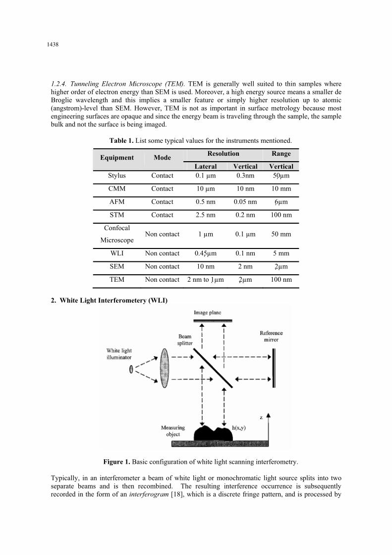