PCM Codec - Texas Instruments
40
TLV320AIC1110 SLAS359 – DECEMBER 2001 PCM CODEC 1 www.ti.com FEATURES D 2.7-V to 3.3-V Operation D Designed for Analog and Digital Wireless Handsets and Telecommunications Applications D Two Differential Microphone Inputs D Differential Earphone Outputs and One Single-Ended Earphone Output D Earphone and Microphone Mute D Programmable Transmit, Receive, and Sidetone Paths With Extended Gain and Attenuation Ranges D Programmable for 15-Bit Linear Data or 8-Bit Companded (µ-law and A-law) Mode D Supports PCM Clock Rates of 128 kHz and 2.048 MHz D Pulse Density Modulated (PDM) Buzzer Output D On-Chip I 2 C Bus, Which Provides Simple, Standard, Two-Wire Serial Interface With Digital ICs D Dual-Tone Multifrequency (DTMF) and Single-Tone Generator Capable of up to 8-kHz Tone With Three Selectable Resolutions of 7.8125 Hz, 15.625 Hz, and 31.25 Hz D 2-Channel Auxiliary Multiplexer (MUX) (Analog Switch) { D Capable of Driving 32 Ω Down to a 8-Ω Speaker D Programmable Power Down Modes D Pin Compatible to the TLV320AIC1103 and TLV320AIC1109 Devices for TQFP Only D Available in a 32-Pin Thin Quad Flatpack (TQFP) Package and MicroStar Juniort BGA APPLICATIONS D Digital Handset D Digital Headset D Cordless Phones D Digital PABX D Digital Voice Recording DESCRIPTION The TLV320AIC1110 provides extended gain and attenuation flexibility for transmit, receive, and sidetone paths. A differential earphone output is capable of driving speaker loads as low as 8 Ω for use in speaker phone applications. The single tone function on the TLV320AIC1110 generates a single tone output of up to 8 kHz. The resolution of the DTMF tone is also selectable to 7.8125 Hz, 15.625 Hz, or 31.25 Hz through the interface control. The analog switch provides more control capabilities for voice-band audio processor (PCM codec). This device contains circuits to protect its inputs and outputs against damage due to high static voltages or electrostatic fields. These circuits have been qualified to protect this device against electrostatic discharges (ESD) of up to 2 kV according to MIL-STD-883C, Method 3015; however, it is advised that precautions be taken to avoid application of any voltage higher than maximum-rated voltages to these high-impedance circuits. During storage or handling, the device leads should be shorted together or the device should be placed in conductive foam. In a circuit, unused inputs should always be connected to an appropriated logic voltage level, preferably either V CC or ground. Specific guidelines for handling devices of this type are contained in the publication Guidelines for Handling Electrostatic-Discharge-Sensitive (ESDS) Devices and Assemblies available from Texas Instruments. Please be aware that an important notice concerning availability, standard warranty, and use in critical applications of Texas Instruments semiconductor products and disclaimers thereto appears at the end of this data sheet. PRODUCTION DATA information is current as of publication date. Products conform to specifications per the terms of Texas Instruments standard warranty. Production processing does not necessarily include testing of all parameters. Copyright 2001, Texas Instruments Incorporated † These options are available on some devices. Please see the table of comparison for the last two generations of PCM codecs. MicroStar Junior is a trademark of Texas Instruments. All other trademarks are the property of their respective owners.
Transcript of PCM Codec - Texas Instruments

TLV320AIC1110
SLAS359 – DECEMBER 2001
PCM CODEC
1www.ti.com
FEATURES 2.7-V to 3.3-V Operation
Designed for Analog and Digital WirelessHandsets and TelecommunicationsApplications
Two Differential Microphone Inputs
Differential Earphone Outputs and OneSingle-Ended Earphone Output
Earphone and Microphone Mute
Programmable Transmit, Receive, andSidetone Paths With Extended Gain andAttenuation Ranges
Programmable for 15-Bit Linear Data or 8-BitCompanded (µ-law and A-law) Mode
Supports PCM Clock Rates of 128 kHz and2.048 MHz
Pulse Density Modulated (PDM) BuzzerOutput
On-Chip I2C Bus, Which Provides Simple,Standard, Two-Wire Serial Interface WithDigital ICs
Dual-Tone Multifrequency (DTMF) andSingle-Tone Generator Capable of up to 8-kHzTone With Three Selectable Resolutions of7.8125 Hz, 15.625 Hz, and 31.25 Hz
2-Channel Auxiliary Multiplexer (MUX) (AnalogSwitch)
Capable of Driving 32 Ω Down to a 8-ΩSpeaker
Programmable Power Down Modes
Pin Compatible to the TLV320AIC1103 andTLV320AIC1109 Devices for TQFP Only
Available in a 32-Pin Thin Quad Flatpack(TQFP) Package and MicroStar Junior BGA
APPLICATIONS Digital Handset
Digital Headset
Cordless Phones
Digital PABX
Digital Voice Recording
DESCRIPTION
The TLV320AIC1110 provides extended gain andattenuation flexibility for transmit, receive, and sidetonepaths. A differential earphone output is capable ofdriving speaker loads as low as 8 Ω for use in speakerphone applications. The single tone function on theTLV320AIC1110 generates a single tone output of up to8 kHz. The resolution of the DTMF tone is alsoselectable to 7.8125 Hz, 15.625 Hz, or 31.25 Hz throughthe interface control. The analog switch provides morecontrol capabilities for voice-band audio processor(PCM codec).
This device contains circuits to protect its inputs and outputs against damage due to high static voltages or electrostatic fields. Thesecircuits have been qualified to protect this device against electrostatic discharges (ESD) of up to 2 kV according to MIL-STD-883C,Method 3015; however, it is advised that precautions be taken to avoid application of any voltage higher than maximum-ratedvoltages to these high-impedance circuits. During storage or handling, the device leads should be shorted together or the deviceshould be placed in conductive foam. In a circuit, unused inputs should always be connected to an appropriated logic voltage level,preferably either VCC or ground. Specific guidelines for handling devices of this type are contained in the publication Guidelines forHandling Electrostatic-Discharge-Sensitive (ESDS) Devices and Assemblies available from Texas Instruments.
Please be aware that an important notice concerning availability, standard warranty, and use in critical applications ofTexas Instruments semiconductor products and disclaimers thereto appears at the end of this data sheet.
PRODUCTION DATA information is current as of publication date.Products conform to specifications per the terms of Texas Instrumentsstandard warranty. Production processing does not necessarily includetesting of all parameters.
Copyright 2001, Texas Instruments Incorporated
†These options are available on some devices. Please see the table of comparison for the last two generations of PCM codecs.MicroStar Junior is a trademark of Texas Instruments.All other trademarks are the property of their respective owners.

TLV320AIC1110
SLAS359 – DECEMBER 2001
2 www.ti.com
DESCRIPTION (Continued)
The PCM codec is an analog-digital interface for voice band signals designed with a combination of coders anddecoders (codecs) and filters. It is a low-power device with companding options and programming features, andit meets the requirements for communication systems, including the cellular phone. The device operates ineither the 15-bit linear or 8-bit companded (µ-law or A-Law) mode, which is selectable through the I2C interface.
A coder, an analog-to-digital converter or ADC, digitizes the analog voice signal, and a decoder, adigital-to-analog converter or DAC, converts the digital-voice signal to an analog output. The PCM codecprovides a companding option to overcome the bandwidth limitations of telephone networks without degradingthe sound quality. The human auditory system is a logarithmic system in which high amplitude signals requireless resolution than low amplitude signals. Therefore, an 8-bit code word with nonuniform quantization (µ-lawor A-law) has the same quality as 13-bit linear coding. The PCM codec provides better digital code words bygenerating a 15-bit linear coding option.
The human voice is effective from a frequency range of 300 Hz to 3300 Hz in telephony applications. In orderto eliminate unwanted signals, the PCM codec design has two types of filters that operate in both the transmitand receive path. A low-pass filter attenuates the signals over 4 kHz. A selectable high-pass filter cleans up thesignals under 100 Hz. This reduces noise that may have coupled in from 50/60-Hz power cables. The high-passfilter is bypassed by selecting the corresponding register bit.
The PCM codec has many programming features that are controlled using a 2-wire standard serial I2C interface.This allows the device to interface with many digital ICs such as a DSP or a microprocessor. The device hasseven registers: power control, mode control, transmit PGA, receive PGA, high DTMF, low DTMF, and auxiliarymode control. Some of the programmable features that can be controlled by I2C interface include:
Transmit amplifier gain
Receive amplifier gain
Sidetone gain
Volume control
Earphone control
PLL power control
Microphone selection
Transmit channel high-pass filter control
Receive channel high-pass filter control
Companding options and selection control
PCM loopback
DTMF control
Pulse density modulated control
The PCM codec is also capable of generating its own internal clocks from a 2.048-MHz master clock input.

TLV320AIC1110
SLAS359 – DECEMBER 2001
3www.ti.com
PBS PACKAGE(TOP VIEW)
31
3029
28
27
910
PCMOPCMIDVSSDVDDSCLSDAMUXOUT2MUXOUT1
PLLVDDEARVSSEAR1ONEARVDDEAR1OPEARVSSEAR2O
AVDD 32
26
11
12
13
14
15
MB
IAS
MIC
1PM
IC1N
MIC
2P
MU
XIN
1625
1 2 3 4 5 6 7 8
24 23 22 21 20 19 18 17
MIC
2NR
EX
T
AV
SS
MC
LK
PLL
VS
SV
SS
RE
SE
TP
WR
UP
SE
LB
UZ
ZC
ON
PC
MS
YN
PC
MC
LK

TLV320AIC1110
SLAS359 – DECEMBER 2001
4 www.ti.com
98765
A
B
C
D
E
F
321
G
H
J
4
AVDD
BUZZCON
PCMSYN
PCMCLK
PCMO
MUXIN
MBIAS
RESET
MCLK
PWRUPSEL
AVSS
MIC2P
MIC1P
MIC1N
REXT
MIC2N
NCNC
NC
NC
NC
NC
NC
NCNC NC NC NC
NC NC NC
NC NC NC
NC NC NC
NC NC
NC NC NC
VSSNCNCNC
NCNC
NC
NC
NCNC NC
NCNC NC
NC NC
NC
NC
NC
NC
NCNC
NC
PLL
VS
S
PLL
VD
D
EA
RV
SS
EA
R1O
N
EA
R1O
P
EA
RV
SS
EA
R2O
MU
XO
UT
1
MU
XO
UT
2
SD
A
SC
L
DV
DD
DV
SS
PC
MI
EA
RV
DD
MicroStar Junior (GQE) PACKAGE(TOP VIEW)

TLV320AIC1110
SLA
S359 – D
EC
EM
BE
R 20015
ww
w.ti.co
m
fun
ction
al blo
ck diag
ram
PCMIN
PCMSYN
PCMCLK
MIC1P
MIC1N
MIC2P
MIC2N
MICAmplifier
1g =
23.5 dB
MICAmplifier
2g = 6
or18 dB
AnalogModulator
TX Filterand PGA
g = –10 dBto
0 dB
PCMInterface
Sidetoneg = –24 db
to–12 dB
RX VolControl
g = –18 dBto
0 dB
RX Filterand PGAg = – 6 dB
to+6 dB
DigitalModulatorand Filter
EarAmp1
EarAmp2
DTMF
Generator
Control Bus
REF PLL
BuzzerControl
Power and RESET
SC
LK
SD
ATA
MB
IAS
RE
XT
MC
LK
RE
SE
T SS
EA
RV
DD
EA
RV S
SP
LLV
DD
PLLV S
SD
V
DD
DV
SS
AV
DD
AV S
SV P
WR
UP
SE
L
PCMOUT
EAR1OP
EAR1ON
EAR2O
BUZZCON
DTMFGAIN
DTMF
Voice0 dB
or6 dB
MUX
–12 to12 dBin 6dBSteps
I C
MUXINOUT
OUT
I/F
2

TLV320AIC1110
SLAS359 – DECEMBER 2001
6 www.ti.com
detailed description
power on/reset
The power for the various digital and analog circuits is separated to improve the noise performance of thedevice. An external reset must be applied to the active low RESET terminal to assure reset upon power on andto bring the device to an operational state. After the initial power-on sequence, the device can be functionallypowered up and powered down by writing to the power control register through the I2C interface. The devicehas a pin-selectable power up in the default mode option. The hardwired pin-selectable PWRUPSEL functionallows the PCM codec to power up in the default mode and to be used without a microcontroller.
reference
A precision band gap reference voltage is generated internally and supplies all required voltage references tooperate the transmit and receive channels. The reference system also supplies bias voltage for use with anelectret microphone at terminal MBIAS. An external precision resistor is required for reference current settingat terminal REXT.
I2C control interface
The I2C interface is a two-wire bidirectional serial interface. The I2C interface controls the PCM codec by writingdata to seven control registers:
Power control
Mode control
Transmit PGA and sidetone control
Receive PGA gain and volume control
DTMF routing
Tone selection control
Auxiliary control
There are two power-up modes which may be selected at the PWRUPSEL terminal: (1) The PWRUPSEL state(VDD at terminal 20) causes the device to power up in the default mode when power is applied. Without an I2Cinterface or controlling device, the programmable functions are fixed at the default gain levels, and functionssuch as the sidetone and DTMF are not accessible. (2) The PWRUPSEL state (ground at terminal 20) causesthe device to go to a power-down state when power is applied. In this mode, an I2C interface is required to powerup the device.
phase-locked loop (PLL)
The phase-lock loop generates the internal clock frequency required for digital filters and modulators by phaselocking to 2.048-MHz master clock input.
PCM interface
The PCM interface transmits and receives data at the PCMO and PCMI terminals respectively. The data istransmitted or received at the PCMCLK speed once every PCMSYN cycle. The PCMCLK can be tied directlyto the 128-kHz or 2.048-MHz master clock (MCLK). The PCMSYN can be driven by an external source orderived from the master clock and used as an interrupt to the host controller.
microphone amplifiers
The microphone input is a switchable interface for two differential microphone inputs. The first stage is alow-noise differential amplifier that provides a gain of 23.5 dB. The second-stage amplifier has a selectable gainof 6 dB or 18 dB.

TLV320AIC1110
SLAS359 – DECEMBER 2001
7www.ti.com
detailed description (continued)
analog modulator
The transmit channel modulator is a third-order sigma-delta design.
transmit filter and PGA
The transmit filter is a digital filter designed to meet CCITT G.714 requirements. The device operates either inthe 15-bit linear or 8-bit companded µ-law or in the A-law mode, which is selectable through the I2C interface.The transmit PGA defaults to 0 dB.
sidetone
A portion of the transmitted audio is attenuated and fed back to the receive channel through the sidetone path.The sidetone path defaults to the mute condition. The default gain of -12 dB is set in the sidetone control register.The sidetone path can be enabled by writing to the power control register.
receive volume control
The receive volume control block acts as an attenuator with a range of –18 dB to 0 dB in 2-dB steps for controlof the receive channel volume. The receive volume control gain defaults to 0 dB.
receive filter and PGA
The receive filter is a digital filter that meets CCITT G.714 requirements with a high-pass filter that is selectablethrough the I2C interface. The device operates either in the 15-bit linear or the 8-bit µ-law or the A-lawcompanded mode, which is selectable through the I2C interface. The gain defaults to –4 dB, representing a3-dBm level for a 32-Ω load impedance and the corresponding digital full scale PCMI code.
digital modulator and filter
The second-order digital modulator and filter convert the received digital PCM data to the analog output requiredby the earphone interface.
earphone amplifiers
The analog signal can be routed to either of two earphone amplifiers, one with differential output (EAR1ON andEAR1OP) and one with single-ended output (EAR2O). Clicks and pops are suppressed for EAR1 differentialoutput only.
tone generator
The tone generator provides generation of standard DTMF tones which are output to (1) the buzzer driver, asa PDM signal, (2) the receive path DAC for outputting through the earphone, or (3) as PCMO data. The integervalue is loaded into one of two 8-bit registers, the high-tone register (04), or the low-tone register (05) (see theRegister Map Addressing section). The tone output is 2 dB higher when applied to the high tone register (04).The high DTMF tones must be applied to the high-tone register, and the low DTMF tones to the low-tone register.The tone signals can be generated with three different resolutions at ∆F= 7.8125 Hz, 15.625 Hz, and 31.250 Hz.The resolution option can be selected by setting the register (06).
analog mux
The analog switch can be used to source an analog signal to two different loads. The output can be reselectedby setting the auxiliary register (06).

TLV320AIC1110
SLAS359 – DECEMBER 2001
8 www.ti.com
detailed description (continued)
DTMF gain MUX
The DTMF gain MUX selects the signal path and applies the appropriate gain setting. Therefore the device iseither in tone mode or in voice mode. When set in the voice mode, the gain is controlled by the auxiliary registerand is set to 0 dB or 6 dB. When set in the tone mode, the gain is from –12 dB to 12 dB in 6-dB steps whichis set by the volume control register. The gain setting is controlled by the RXPGA register. This will not createany control contention since the device is working in one mode at a time.
Terminal Functions
TERMINAL†
NAMENO. I/O DESCRIPTION
NAMEµBGA TQFP
I/O DESCRIPTION
AVDD A1 32 I Analog positive power supply
AVSS J1 8 I Analog negative power supply (use for ground connection)
BUZZCON F9 19 O Buzzer output, a pulse-density modulated signal to apply to external buzzer driver
DVDD J6 13 I Digital positive power supply
DVSS J7 14 I Digital negative power supply
EAR1ON A6 27 O Earphone 1 amplifier output (–)
EAR1OP A4 29 O Earphone 1 amplifier output (+)
EAR2O A2 31 O Earphone 2 amplifier output
EARVDD A5 28 I Analog positive power supply for the earphone amplifiers
EARVSS A3, A7 30, 26 I Analog negative power supply for the earphone amplifiers
MBIAS B1 1 O Microphone bias supply output, no decoupling capacitors
MCLK C9 22 I Master system clock input (2.048 MHz, digital)
MIC1P C1 2 I MIC1 input (+)
MIC1N D1 3 I MIC1 input (–)
MIC2P E1 4 I MIC2 input (+)
MIC2N F1 5 I MIC2 input (–)
MUXIN H1 7 I Analog MUX input
MUXOUT1 J2 9 I Analog MUX output
MUXOUT2 J3 10 I Analog MUX output
PCMI J8 15 I Receive PCM input
PCMO J9 16 O Transmit PCM output
PCMSYN G9 18 I PCM frame sync
PCMCLK H9 17 I PCM data clock
PLLVSS A9 24 I PLL negative power supply
PLLVDD A8 25 I PLL digital power supply
PWRUPSEL E9 20 I Selects the power-up default mode
REXT G1 6 I/O Internal reference current setting terminal (use precision 100-kΩ resistor and no filtering capacitors)
RESET D9 21 I Active low reset
SCL J5 12 I I2C-bus serial clock. This input is used to synchronize the data transfer from and to the PCM codec.
SDA J4 11 I/O I2C-bus serial address/data input/output. This is a bidirectional terminal used to transfer registercontrol addresses and data into and out of the codec. It is an open-drain terminal and thereforerequires a pullup resistor to VDD (typical 10 kΩ for 100 kHz).
VSS B9 23 I Ground return for bandgap internal reference (use for ground connection)
† All MicroStar Junior BGA pins that are not mentioned have no internal connection.

TLV320AIC1110
SLAS359 – DECEMBER 2001
9www.ti.com
absolute maximum ratings over operating free-air temperature range (unless otherwise noted)†
Supply voltage range, AVDD, DVDD, PLLVDD, EARVDD –0.5 V to 3.6 V. . . . . . . . . . . . . . . . . . . . . . . . . . . . . . . . . . . . . Output voltage range, VO –0.5 V to 3.6 V. . . . . . . . . . . . . . . . . . . . . . . . . . . . . . . . . . . . . . . . . . . . . . . . . . . . . . . . . . . . . . . Input voltage range, VI –0.5 V to 3.6 V. . . . . . . . . . . . . . . . . . . . . . . . . . . . . . . . . . . . . . . . . . . . . . . . . . . . . . . . . . . . . . . . . . Continuous total power dissipation See Dissipation Rating Table. . . . . . . . . . . . . . . . . . . . . . . . . . . . . . . . . . . . . . . . . . Operating free air temperature range (industrial temperature) –40°C to 85°C. . . . . . . . . . . . . . . . . . . . . . . . . . . . . . . . Storage temperature range, testing –65°C to 150°C. . . . . . . . . . . . . . . . . . . . . . . . . . . . . . . . . . . . . . . . . . . . . . . . . . . . . . Lead temperature 1,6 mm from case for 10 seconds 260°C. . . . . . . . . . . . . . . . . . . . . . . . . . . . . . . . . . . . . . . . . . . . . . . † Stresses beyond those listed under “absolute maximum ratings” may cause permanent damage to the device. These are stress ratings only, and
functional operation of the device at these or any other conditions beyond those indicated under “recommended operating conditions” is notimplied. Exposure to absolute-maximum-rated conditions for extended periods may affect device reliability.
DISSIPATION RATING TABLE
PACKAGETA ≤ 25°C
POWER RATINGDERATING FACTORABOVE TA = 25°C
TA = 85°CPOWER RATING COMMENTS
TQFP 702 mW 7.2 mW/°C 270 mW Low dissipation printedcircuit board (PCB)
MicroStar Junior BGA 660 mW 164 mW/°C 220 mW Low dissipation PCB
MicroStar Junior BGA 2.75 W 36 mW/°C 917 mW High dissipation PCB
recommended operating conditions (see Notes 1 and 2)
MIN NOM MAX UNIT
Supply voltage, AVDD, DVDD, PLLVDD, EARVDD 2.7 3.3 V
High-level input voltage, VIH 0.7xVDD V
Low-level input voltage, VIL 0.3xVDD V
Load impedance between EAR1OP and EAR1ON-RL 8 to 32 Ω
Load impedance for EAR2OP-RL 32 Ω
Operating free-air temperature, TA –40 85 C
NOTES: 1. To avoid possible damage and resulting reliability problems to these CMOS devices, follow the power-on initialization paragraph,described in the Principles of Operation.
2. Voltages are with respect to AVSS, DVSS, PLLVSS, and EARVSS.
electrical characteristics over recommended ranges of supply voltage and free-air temperature (unlessotherwise noted)
supply currentPARAMETER TEST CONDITIONS MIN TYP MAX UNIT
Operating, EAR1 selected, MicBias disabled 4.5 6 mA
Operating, EAR2 selected, MicBias disabled 4.5 6 mA
IDD Supply current from VDDPower down room temperature, VDD = 3 V, Reg 6 bit 7 = 1, MClknot present (see Note 3) 2 10 µA
Power down room temperature, VDD = 3 V, , Reg 6 bit 7 = 0,MClk not present (see Note 3) 10 30 µA
ton(i)Power-up time frompower down 5 10 ms
NOTE 3: VIHMIN = VDD, VILMAX = VSS.

TLV320AIC1110
SLAS359 – DECEMBER 2001
10 www.ti.com
electrical characteristics over recommended ranges of supply voltage and free-air temperature (unlessotherwise noted) (continued)
digital interfacePARAMETER TEST CONDITIONS MIN TYP MAX UNIT
VOH High-level output voltage PCMO (BUZZCON) IOH = –3.2 mA, VDD = 3 V DVDD–0.25 V
VOL Low-level output voltage PCMO IOL = 3.2 mA, VDD = 3 V 0.25 V
IIH High-level input current, any digital input VI = VDD 10 µA
IIL Low-level input current, any digital input VI = VSS 10 µA
Ci Input capacitance 10 pF
Co Output capacitance 20 pF
RL Load impedance (BUZZCON) 5 kΩ
microphone interfacePARAMETER TEST CONDITIONS MIN TYP MAX UNIT
VIO Input offset voltage at MIC1N, MIC2N See Note 4 –5 5 mV
IIB Input bias current at MIC1N, MIC2N –300 300 nA
Ci Input capacitance at MIC1N, MIC2N 5 pF
VnMicrophone input referred noise, psophometrically weighted,(C-message weighted is similar)
MIC amp 1 gain = 23.5 dBMIC amp 2 gain = 0 dB
3 4.7 µVrms
IOmax Output source current—MBIAS 1 1.2 mA
V(mbias) Microphone bias supply voltage (see Note 5) 2.3 2.5 2.65 V
MICMUTE –80 dB
Input impedance Fully differential 35 60 100 kΩ
NOTES: 4. Measured while MIC1P and MIC1N are connected together. Less than 0.5-mV offset results in 0 value code on PCMOUT.5. Not a JEDEC symbol.

TLV320AIC1110
SLAS359 – DECEMBER 2001
11www.ti.com
electrical characteristics over recommended ranges of supply voltage and free-air temperature (unlessotherwise noted) (continued)
speaker interfacePARAMETER TEST CONDITIONS MIN TYP MAX UNIT
VDD = 2.7 V, fully differential, 8-Ω load,3-dBm0 output, volume control = –3 dB,RXPGA = –4 dB level
161 200
Earphone AMP1 output power (see Note 6)VDD = 2.7 V, fully differential, 16-Ω load,3-dBm0 output, volume control = –3 dB,RXPGA = –2 dB level
128 160 mW
VDD = 2.7 V, fully differential, 32-Ω load,3-dBm0 output, volume control = –3 dB,RXPGA = –1 dB level
81 100
Earphone AMP2 output power (see Note 6)VDD = 2.7 V, single-ended, 32-Ω load,3-dBm0 output
10 12.5 mW
VOO Output offset voltage at EAR1 Fully differential ±5 ±30 mV
3-dBm0 input, 8-Ω load 141 178
I maxMaximum output current for EAR1 (rms) 3-dBm0 input, 16-Ω load 90 112
mAIOmaxMaximum out ut current for EAR1 (rms)
3-dBm0 input, 32-Ω load 50 63mA
Maximum output current for EAR2 (rms) 3-dBm0 input 17.7 22.1
EARMUTE –80 dB
NOTE 6: Maximum power is with a load impedance of –25%.
transmit gain and dynamic range, companded mode (µ-law or A-law) or linear mode selected, transmit slopefilter bypassed (see Notes 7 and 8)
PARAMETER TEST CONDITIONS MIN TYP MAX UNIT
Transmit reference-signal level (0 dB) Differential 87.5 mVpp
Overload signal level (3 dBm0)Differential, normal mode 124
mVOverload-signal level (3 dBm0)Differential, extended mode 31.5
mVpp
Absolute gain error 0-dBm0 input signal, VDD ±10% –1 1 dB
G i ith i t l l l ti t i tMIC1N, MIC1P to PCMO at 3 dBm0 to –30 dBm0 –0.5 0.5
Gain error with input level relative to gain at–10 dBm0 MIC1N MIC1P to PCMO
MIC1N, MIC1P to PCMO at –31 dBm0 to –45 dBm0 –1 1 dB–10 dBm0 MIC1N, MIC1P to PCMOMIC1N, MIC1P to PCMO at –46 dBm0 to –55 dBm0 –1.2 1.2
dB
NOTES: 7. Unless otherwise noted, the analog input is 0 dB, 1020-Hz sine wave, where 0 dB is defined as the zero-reference point of the channelunder test.
8. The reference signal level, which is input to the transmit channel, is defined as a value 3 dB below the full-scale value of 88-mVrms.
transmit gain and dynamic range, companded mode (µ-law or A-law) or linear mode selected, transmit slopefilter enabled (see Notes 7 and 8)
PARAMETER TEST CONDITIONS MIN TYP MAX UNIT
Transmit reference-signal level (0 dB) Differential 87.5 mVpp
Overload signal level (3 dBm0)Differential, normal mode 124
mVOverload-signal level (3 dBm0)Differential, extended mode 31.5
mVpp
Absolute gain error 0-dBm0 input signal, VDD ±10% –1 1 dB
G i ith i t l l l ti t i tMIC1N, MIC1P to PCMO at 3 dBm0 to –30 dBm0 –0.5 0.5
Gain error with input level relative to gain at–10 dBm0 MIC1N MIC1P to PCMO
MIC1N, MIC1P to PCMO at –31 dBm0 to –45 dBm0 –1 1 dB–10 dBm0 MIC1N, MIC1P to PCMOMIC1N, MIC1P to PCMO at –46 dBm0 to –55 dBm0 –1.2 1.2
dB
NOTES: 7. Unless otherwise noted, the analog input is 0 dB, 1020-Hz sine wave, where 0 dB is defined as the zero-reference point of thechannel under test.
8 The reference signal level, which is input to the transmit channel, is defined as a value 3 dB below the full-scale value of 88-mVrms.

TLV320AIC1110
SLAS359 – DECEMBER 2001
12 www.ti.com
electrical characteristics over recommended ranges of supply voltage and free-air temperature (unlessotherwise noted) (continued)
transmit filter transfer, companded mode (µ-law or A-law) or linear mode selected, transmit slope filterbypassed (MCLK = 2.048 MHz)
PARAMETER TEST CONDITIONS MIN TYP MAX UNIT
fMIC1 or fMIC2 <100 Hz –0.5 0.5
fMIC1 or fMIC2 = 200 Hz –0.5 0.5
G i l ti t i t i l i t 1020 H i t l hi hfMIC1 or fMIC2 = 300 Hz to 3 kHz –0.5 0.5
Gain relative to input signal gain at 1020 Hz, internal high-passfilter disabled
fMIC1 or fMIC2 = 3.4 kHz –1.5 0 dBfilter disabledfMIC1 or fMIC2 = 4 kHz –14
dB
fMIC1 or fMIC2 = 4.6 kHz –35
fMIC1 or fMIC2 = 8 kHz –47
Gain relative to input signal gain at 1020 Hz, internal high-pass fMIC1 or fMIC2 < 100 Hz –15dB
Gain relative to in ut signal gain at 1020 Hz, internal high assfilter enabled fMIC1 or fMIC2 = 200 Hz –5
dB
transmit filter transfer, companded mode (µ-law or A-law) or linear mode selected, transmit slope filterselected, transmit high-pass filter enabled (MCLK = 2.048 MHz) (see Note 9)
PARAMETER TEST CONDITIONS MIN TYP MAX UNIT
fMIC1 or f MIC2 =100 Hz –27 dB
fMIC1 or fMIC2 = 200 Hz –8 dB
fMIC1 or fMIC2 = 250 Hz –4 dB
fMIC1 or fMIC2 = 300 Hz –1.8 dB
fMIC1 or fMIC2 = 400 Hz –1.5 dB
fMIC1 or fMIC2 = 500 Hz –1.3 dB
fMIC1 or fMIC2 = 600 Hz –1.1 dB
fMIC1 or fMIC2 = 700 Hz –0.8 dB
fMIC1 or fMIC2 = 800 Hz –0.57 dB
fMIC1 or fMIC2 = 900 Hz –0.25 dB
Gain relative to input signal gain at 1.02 kHz, with slope filter fMIC1 or fMIC2 = 1000 Hz 0 dBGain relative to in ut signal gain at 1.02 kHz, with slo e filterselected fMIC1 or fMIC2 = 1500 Hz 1.8 dB
fMIC1 or fMIC2 = 2000 Hz 4.0 dB
fMIC1 or fMIC2 = 2500 Hz 6.5 dB
fMIC1 or fMIC2 = 3000 Hz 7.6 dB
fMIC1 or fMIC2 = 3100 Hz 7.7 dB
fMIC1 or fMIC2 = 3300 Hz 8 dB
fMIC1 or fMIC2 = 3500 Hz 6.48 dB
fMIC1 or fMIC2 = 4000 Hz –13 dB
fMIC1 or fMIC2 = 4500 Hz –35 dB
fMIC1 or fMIC2 = 5000 Hz –45 dB
fMIC1 or fMIC2 = 8000 Hz –50 dB
NOTE 9: The pass-band tolerance is ±0.25 dB from 300 Hz to 3500 Hz.

TLV320AIC1110
SLAS359 – DECEMBER 2001
13www.ti.com
electrical characteristics over recommended ranges of supply voltage and free-air temperature (unlessotherwise noted) (continued)
transmit idle channel noise and distortion, companded mode (µ-law or A-law) selected, slope filter bypassedPARAMETER TEST CONDITIONS MIN TYP MAX UNIT
Transmit idle channel noise, psophometricallyweighted
TXPGA gain= 0 dB, MIC Amp 1 gain = 23.5 dB,MIC Amp 2 gain = 6 dB
–83.5 –78 dBm0p
MIC1N, MIC1P to PCMO at 3 dBm0 27
MIC1N, MIC1P to PCMO at 0 dBm0 30
MIC1N, MIC1P to PCMO at –5 dBm0 33
Transmit signal-to-distortion ratio with MIC1N, MIC1P to PCMO at –10 dBm0 36dBm0
Transmit signal to distortion ratio with1020-Hz sine-wave input MIC1N, MIC1P to PCMO at –20 dBm0 35
dBm0
MIC1N, MIC1P to PCMO at – 30 dBm0 26
MIC1N, MIC1P to PCMO at – 40 dBm0 24
MIC1N, MIC1P to PCMO at – 45 dBm0 19
Intermodulation distortion, 2-tone CCITT method, CCITT G.712 (7.1), R2 49dB
Intermodulation distortion, 2 tone CCITT method,composite power level, –13 dBm0 CCITT G.712 (7.2), R2 51
dB
transmit idle channel noise and distortion, companded mode (µ-law or A-law) selected, slope filter enabledPARAMETER TEST CONDITIONS MIN TYP MAX UNIT
Transmit idle channel noise, psophometricallyweighted
TXPGA gain= 0 dB, MIC Amp 1 gain = 23.5 dB,MIC Amp 2 gain = 6 dB
–83.5 –78 dBm0p
MIC1N, MIC1P to PCMO at 3 dBm0 27
MIC1N, MIC1P to PCMO at 0 dBm0 30
MIC1N, MIC1P to PCMO at –5 dBm0 33
Transmit signal-to-total distortion ratio with 1020-Hz MIC1N, MIC1P to PCMO at –10 dBm0 36dBm0
Transmit signal to total distortion ratio with 1020 Hzsine-wave input MIC1N, MIC1P to PCMO at –20 dBm0 35
dBm0
MIC1N, MIC1P to PCMO at –30 dBm0 26
MIC1N, MIC1P to PCMO at –40 dBm0 24
MIC1N, MIC1P to PCMO at –45 dBm0 19
Intermodulation distortion, 2-tone CCITT method, CCITT G.712 (7.1), R2 49dB
Intermodulation distortion, 2 tone CCITT method, composite power level, –13 dBm0 CCITT G.712 (7.2), R2 51
dB
transmit idle channel noise and distortion, linear mode selected, slope filter bypassedPARAMETER TEST CONDITIONS MIN TYP MAX UNIT
Transmit idle channel noiseTXPGA gain = 0 dB, MIC Amp 1 gain = 23.5 dB,MIC Amp 2 gain = 6 dB
–83.5 –78 dBm0p
MIC1N, MIC1P to PCMO at 3 dBm0 50 50
MIC1N, MIC1P to PCMO at 0 dBm0 50 65
MIC1N, MIC1P to PCMO at –5 dBm0 52 61
Transmit signal-to-total distortion ratio with 1020-Hz MIC1N, MIC1P to PCMO at –10 dBm0 56 65dB
Transmit signal to total distortion ratio with 1020 Hzsine-wave input MIC1N, MIC1P to PCMO at –20 dBm0 50 59
dB
MIC1N, MIC1P to PCMO at –30 dBm0 51 63
MIC1N, MIC1P to PCMO at –40 dBm0 43 55
MIC1N, MIC1P to PCMO at –45 dBm0 38 52

TLV320AIC1110
SLAS359 – DECEMBER 2001
14 www.ti.com
electrical characteristics over recommended ranges of supply voltage and free-air temperature (unlessotherwise noted) (continued)
transmit idle channel noise and distortion, linear mode selected, slope filter enabledPARAMETER TEST CONDITIONS MIN TYP MAX UNIT
Transmit idle channel noiseTXPGA gain = 0 dB, MIC Amp 1 gain = 23.5 dB,MIC Amp 2 gain = 6 dB
–83.5 –78 dBm0p
MIC1N, MIC1P to PCMO at 3 dBm0 40 50
MIC1N, MIC1P to PCMO at 0 dBm0 50 65
MIC1N, MIC1P to PCMO at –5 dBm0 50 68
Transmit signal-to-total distortion ratio with MIC1N, MIC1P to PCMO at –10 dBm0 64 70dB
Transmit signal to total distortion ratio with1020-Hz sine-wave input MIC1N, MIC1P to PCMO at –20 dBm0 58 65
dB
MIC1N, MIC1P to PCMO at –30 dBm0 50 60
MIC1N, MIC1P to PCMO at –40 dBm0 38 50
MIC1N, MIC1P to PCMO at –45 dBm0 30 45
receive gain and dynamic range, EAR1 selected, linear or companded (µ-law or A-law) mode selected (seeNote 10)
PARAMETER TEST CONDITIONS MIN TYP MAX UNIT
8-Ω load RXPGA = –4 dB 3.2
Overload signal level (3 dB) 16-Ω load RXPGA = –4 dB 4.05 VppOverload signal level (3 dB)
32-Ω load RXPGA = –4 dB 4.54
V
Absolute gain error 0 dBm0 input signal, VDD ±10% –1 1 dB
G i ith t t l l l ti t iPCMIN to EAR1ON, EAR1OP at 3 dBm0 to –40 dBm0 –0.5 0.5
Gain error with output level relative to gainat –10 dBm0
PCMIN to EAR1ON, EAR1OP at –41 dBm0 to –50 dBm0 –1 1 dBat –10 dBm0PCMIN to EAR1ON, EAR1OP at –51 dBm0 to –55 dBm0 –1.2 1.2
dB
NOTE 10: RXPGA = –4 dB for 32 Ω , 16 Ω , or 8 Ω, RXVOL = 0 dB, 1020-Hz input signal at PCMI, output measured differentially between EAR1ONand EAR1OP
receive gain and dynamic range, EAR2 selected, linear or companded (µ-law or A-law) mode selected (seeNote 11)
PARAMETER TEST CONDITIONS MIN TYP MAX UNIT
Receive reference signal level (0 dB) 0 dBm0 PCM input signal 1.36 Vpp
Overload-signal level (3 dB) 1.925 Vpp
Absolute gain error 0 dBm0 input signal, VDD ±10% –1 1 dB
G i ith t t l l l ti t iPCMIN to EAR2O at 3 dBm0 to –40 dBm0 –0.5 0.5
Gain error with output level relative to gainat –10 dBm0
PCMIN to EAR2O at –41 dBm0 to –50 dBm0 –1 1 dBat –10 dBm0PCMIN to EAR2O at –51 dBm0 to –55 dBm0 –1.2 1.2
dB
NOTE 11: RXPGA = –1 dB, RXVOL = 0 dB
TLV320AIC1110
SLAS359 – DECEMBER 2001
15www.ti.com
electrical characteristics over recommended ranges of supply voltage and free-air temperature (unlessotherwise noted) (continued)
receive filter transfer, companded mode (µ-law or A-law) or linear mode selected (MCLK = 2.048 MHz) (seeNote 11)
PARAMETER TEST CONDITIONS MIN TYP MAX UNIT
fEAR1 or fEAR2 <100 Hz –0.5 0.5
fEAR1 or fEAR2 = 200 Hz –0.5 0.5
G i l ti t i t i l i t 1020 H i t lfEAR1 or fEAR2 = 300 Hz to 3 kHz –0.5 0.5
Gain relative to input signal gain at 1020 Hz, internalhigh-pass filter disabled
fEAR1 or fEAR2 = 3.4 kHz –1.5 0 dBhigh-pass filter disabledfEAR1 or fEAR2 = 4 kHz –14
dB
fEAR1 or fEAR2 = 4.6 kHz –35
fEAR1 or fEAR2 = 8 kHz –47
Gain relative to input signal gain at 1020 Hz, internal fEAR1 or fEAR2 <100 Hz –15dB
Gain relative to in ut signal gain at 1020 Hz, internalhigh-pass filter enabled fEAR1 or fEAR2 = 200 Hz –5
dB
NOTE 11. RXPGA = –1 dB, RXVOL = 0 dB
receive idle channel noise and distortion, EAR1 selected, companded mode (µ-law or A-law) selected (seeNote 10)
PARAMETER TEST CONDITIONS MIN TYP MAX UNIT
Receive noise, psophometrically weighted PCMIN = 11010101 (A-law) –89 –86 dBm0p
Receive noise, C-message weighted PCMIN = 11111111 (µ-law) 36 50 µVrmsPCMIN to EAR1ON, EAR1OP at 3 dBm0 21
PCMIN to EAR1ON, EAR1OP at 0 dBm0 25
PCMIN to EAR1ON, EAR1OP at –5 dBm0 36
Receive signal-to-distortion ratio with 1020-Hz PCMIN to EAR1ON, EAR1OP at –10 dBm0 43dB
Receive signal to distortion ratio with 1020 Hzsinewave input PCMIN to EAR1ON, EAR1OP at –20 dBm0 40
dB
PCMIN to EAR1ON, EAR1OP at –30 dBm0 38
PCMIN to EAR1ON, EAR1OP at –40 dBm0 28
PCMIN to EAR1ON, EAR1OP at –45 dBm0 23
NOTE 10: RXPGA = –4 dB for 32 Ω , RXVOL = 0 dB, 1020-Hz input signal at PCMI, output measured differentially between EAR1ON and EAR1OP.
receive idle channel noise and distortion, EAR1 selected, linear mode selected (see Note 10)PARAMETER TEST CONDITIONS MIN TYP MAX UNIT
Receive noise, (20-Hz to 20-kHz brickwall window) PCMIN = 000000000000000 –88 –83 dBm0
PCMIN to EAR1ON, EAR1OP at 3 dBm0 53 61
PCMIN to EAR1ON, EAR1OP at 0 dBm0 63 75
PCMIN to EAR1ON, EAR1OP at –5 dBm0 60 72
Receive signal-to-distortion ratio with 1020-Hz PCMIN to EAR1ON, EAR1OP at –10 dBm0 56 67dB
Receive signal to distortion ratio with 1020 Hz sine-wave input PCMIN to EAR1ON, EAR1OP at –20 dBm0 50 63
dB
PCMIN to EAR1ON, EAR1OP at –30 dBm0 45 50
PCMIN to EAR1ON, EAR1OP at –40 dBm0 40 51
PCMIN to EAR1ON, EAR1OP at –45 dBm0 38 49
Intermodulation distortion, 2-tone CCITT method, CCITT G.712 (7.1), R2 50dB
Intermodulation distortion, 2 tone CCITT method, composite power level, –13 dBm0 CCITT G.712 (7.2), R2 54
dB
NOTE 10: RXPGA = –4 dB for 32 Ω , RXVOL = 0 dB, 1020-Hz input signal at PCMI, output measured differentially between EAR1ON and EAR1OP.

TLV320AIC1110
SLAS359 – DECEMBER 2001
16 www.ti.com
electrical characteristics over recommended ranges of supply voltage and free-air temperature (unlessotherwise noted) (continued)
receive idle channel noise and distortion EAR2 selected, companded mode (µ-law or A-law) selected (see Note 11)
PARAMETER TEST CONDITIONS MIN TYP MAX UNIT
Receive noise, psophometrically weighted PCMIN = 11010101 (A-law) –82 –78 dBmop
Receive noise, C-message weighted PCMIN = 11111111 (µ-law) 36 50 µVrmsPCMIN to EAR2O at 3 dBm0 21
PCMIN to EAR2O at 0 dBm0 25
PCMIN to EAR2O at –5 dBm0 36
Receive signal to distortion ratio with 1020 Hz sinewave inputPCMIN to EAR2O at –10 dBm0 43
dBReceive signal-to-distortion ratio with 1020-Hz sinewave inputPCMIN to EAR2O at –20 dBm0 40
dB
PCMIN to EAR2O at –30 dBm0 38
PCMIN to EAR2O at –40 dBm0 28
PCMIN to EAR2O at –45 dBm0 23
NOTE 11. RXPGA = –1 dB, RXVOL = 0 dB
receive idle channel noise and distortion, EAR2 selected, linear mode selected (see Note 11)PARAMETER TEST CONDITIONS MIN TYP MAX UNIT
Receive noise, (20-Hz to 20-kHz brickwall window) PCMIN = 000000000000000 –83 –86 dBm0
PCMIN to EAR2O at 3 dBm0 53 60
PCMIN to EAR2O at 0 dBm0 60 65
PCMIN to EAR2O at –5 dBm0 58 62Receive signal-to-noise + distortion ratio with 1020-Hz sinewaveinput
PCMIN to EAR2O at –10 dBm0 55 60dBinput
PCMIN to EAR2O at –20 dBm0 53 60dB
PCMIN to EAR2O at –30 dBm0 51 58
PCMIN to EAR2O at –40 dBm0 50 57
PCMIN to EAR2O at –45 dBm0 48 52
Intermodulation distortion 2 tone CCITT methodCCITT G.712 (7.1), R2 50
dBIntermodulation distortion, 2-tone CCITT methodCCITT G.712 (7.2), R2 54
dB
NOTE 11: RXPGA = –1 dB, RXVOL = 0 dB
power supply rejection and crosstalk attenuationPARAMETER TEST CONDITIONS MIN TYP MAX UNIT
Supply voltage rejection, transmit channelMIC1N, MIC1P =0 V,VDD = 3 Vdc + 100 mVpeak to peak, f = 0 to 50 kHz
– 86 –70 dB
Supply voltage rejection, receive channel,EAR1 selected (differential)
PCM code = positive zero,VDD = 3 Vdc + 100 mVpeak to peak, f = 0 to 50 kHz
– 98 –70 dB
Crosstalk attenuation, transmit-to-receive(differential)
MIC1N, MIC1P = 0 dB, f = 300 to 3400 Hz measured differentially between EAR1ON and EAR1OP
70 dB
Crosstalk attenuation, receive-to-transmitPCMIN = 0 dBm0, f = 300 to 3400 Hz measured atPCMO, EAR1 amplifier
70 dB

TLV320AIC1110
SLAS359 – DECEMBER 2001
17www.ti.com
timing requirements
clock (2.048-MHz CLK)PARAMETER MIN NOM MAX UNIT
tt Transition time, MCLK 10 ns
f(mclk) MCLK frequency 2.048 MHz
MCLK jitter 37%
Number of PCMCLK clock cycles per PCMSYN frame 256 256 cycles
tc(PCMCLK) PCMCLK clock period 156 488 512 ns
Duty cycle, PCMCLK 45% 50% 68%
transmit (2.048-MHz CLK) (see Figure 1)PARAMETER MIN MAX UNIT
tsu(PCMSYN) Setup time, PCMSYN high before falling edge of PCMCLK 20 tc(PCMCLK)–20ns
th(PCMSYN) Hold time, PCMSYN high after falling edge of PCMCLK 20 tc(PCMCLK)–20ns
receive (2.048-MHz CLK) (see Figure 2)PARAMETER MIN MAX UNIT
tsu(PCSYN) Setup time, PCMSYN high before falling edge of PCMCLK 20 tc(PCMCLK)–20 ns
th(PCSYN) Hold time, PCMSYN high after falling edge of PCMCLK 20 tc(PCMCLK)–20 ns
tsu(PCMI) Setup time, PCMI high or low before falling edge of PCMCLK 20 ns
th(PCMI) Hold time, PCMI high or low after falling edge of PCMCLK 20 ns
clock (128-kHz CLK)PARAMETER MIN NOM MAX UNIT
tt Transition time, MCLK 10 ns
f(mclk) MCLK frequency 128 kHz
MCLK jitter 5%
Number of PCMCLK clock cycles per PCMSYN frame 16 16
tc(PCMCLK) PCMCLK clock period 742.19 781.25 820.31 ns
Duty cycle, PCMCLK 40% 50% 60%
tc(PCMSYN) PCMSYN clock period 125 µs
Duty cycle, PCMCLK 49.5% 50% 50.5%
transmit (128-kHz CLK) (see Figure 5)PARAMETER MIN MAX UNIT
tsu(PCMSYN) Setup time, PCMSYN high before PCMCLK↑ 20 tc(PCMCLK)/4ns
th(PCMSYN) Hold time, PCMSYN high after PCMCLK↓ 20 tc(PCMCLK)/4ns
tv(PCMO) Data valid time after the rising edge of PCMSYNC 50 ns
receive (128-kHz CLK) (see Figure 4)PARAMETER MIN MAX UNIT
tsu(PCSYN) Setup time, PCMSYN high before rising edge of PCMCLK 20 tc(PCMCLK)/4 ns
th(PCSYN) Hold time, PCMSYN high after falling edge of PCMCLK 20 tc(PCMCLK)/4 ns
tsu(PCMI) Setup time, PCMI high or low before falling edge of PCMCLK 20 ns
th(PCMI) Hold time, PCMI high or low after falling edge of PCMCLK 20 ns

TLV320AIC1110
SLAS359 – DECEMBER 2001
18 www.ti.com
timing requirements (continued)
I2C bus timing requirements (see Figure 3)
PARAMETER MIN MAX UNIT
SCL Clock frequency 400 kHz
tw(SCLH) Pulse duration, SCL high 600 ns
tw(SCLL) Pulse duration, SCL low 1300 ns
th(STA) Hold time, SCL high after SDA↓ (repeated START condition)† 600 ns
tsu(STA) Setup time, for SCL high before SDA↓ repeated START condition 600 ns
th(DAT) Hold time, SDA valid after SCL low 0 ns
tsu(DAT) Setup time, SDA valid before SCL↑ 100 ns
tsu(STO) Setup time, STOP condition 600 ns
tw(SDAT) Pulse duration, SDA high (bus free time) 1300 ns
tr Rise time (SDA and SCL) 300 ns
tf Fall time (SDA and SCL) 300 ns
† After this period, the first block pulse is generated.
switching characteristics over recommended ranges of supply voltages and operating free-airtemperature
propagation delay times, CL(max) = 10 pF (see Figure 1)
PARAMETER MIN MAX UNIT
tpd1 PCMCLK bit 1 high to PCMO bit 1 valid 35 ns
tpd2 PCMCLK high to PCMO valid, bits 2 to n 35 ns
tpd3 PCMCLK bit n low to PCMO bit n Hi-Z 30 ns
DTMF generatorPARAMETER TEST CONDITIONS MIN TYP MAX UNIT
DTMF high to low tone relative amplitude (preemphasis) 1.5 2 2.5 dB
Tone frequency accuracy (for DTMF) Resolution of 7.8125 Hz –1.5% 1.5%
Harmonic distortionMeasured from lower tone group tohighest parasitic
–20 dB
MICBIASPARAMETER TEST CONDITIONS MIN TYP MAX UNIT
Load impedance (bias mode) 5 kΩ

TLV320AIC1110
SLAS359 – DECEMBER 2001
19www.ti.com
PARAMETER MEASUREMENT INFORMATION
ÎÎÎÎÎÎÎÎÎÎÎÎ
ÎÎÎÎÎÎ
ÎÎÎÎÎÎ
0 1 2 3 4 N–2 N–1 N N+1
Transmit Time Slot
1 2 3 4 N–2 N–1 N
80%20%
tsu(PCMSYN)th(PCMSYN)
See Note A
See Note C
See Note Btpd2
tpd1 See Note D tsu(PCMO)
tpd3
80%20%PCMCLK
PCMSYN
PCMO
NOTES: A. This window is allowed for PCMSYN high.B. This window is allowed for PCMSYN low (th(PCMSYN) max determined by data collision considerations).C. Transitions are measured at 50%.D. Bit 1 = MSB, Bit N = LSB
Figure 1. Transmit Timing Diagram (2.048 MHz)
80%20%
See Note CPCMI
PCMSYN
PCMCLK
0 1 2 3 4 N –2 N –1 N N +1
20%80%
ÎÎÎÎÎÎÎÎÎÎ
ÎÎÎÎÎÎÎÎÎÎÎÎÎÎ
1 2 3 4 N –2 N –1 N
See Note D
th(PCMSYN)tsu(PCMSYN)
See Note A
tsu(PCMI)
th(PCMI)
See Note B
Receive Time Slot
NOTES: A. This window is allowed for PCMSYN high.B. This window is allowed for PCMSYN low.C. Transitions are measured at 50%.D. Bit 1 = MSB, Bit N = LSB
Figure 2. Receive Timing Diagram (2.048 MHz)
thd(STA)
tw(SCLH) tr tf
th(DAT)
tw(SCLH)tsu(DAT)
tsu(STA)
th(STA)
tsu(STO)
STO STA STA STO
SDA
SCL
tw(SDAH)
Figure 3. I2C-Bus Timing Diagram

TLV320AIC1110
SLAS359 – DECEMBER 2001
20 www.ti.com
PARAMETER MEASUREMENT INFORMATION
PCMSYNC
PCMI
PCMCLK
tsu(PCMSYN)
tsu(PCMI)
th(PCMSYN)
th(PCMI)
MSB LSB
Figure 4. Receive Timing Diagram, 128 kHz
PCMSYNC
PCMO
PCMCLK
tsu(PCMSYN)
tv(PCMO)
th(PCMSYN)
MSB LSB
Figure 5. Transmit Timing Diagram, 128 kHz
tc(PCMSYNC)
Figure 6. PCMSYNC Timing, 128 kHz

TLV320AIC1110
SLAS359 – DECEMBER 2001
21www.ti.com
PARAMETER MEASUREMENT INFORMATION
NOTE: SLAVE = Voice Codec
A6 A5 A4 A0 R/W
0
ACK
0
R7 R6 R5 R0 ACK
0
D7 D6 D5 D0 ACK
0
StopSlave Address Register Address Data
SCL
SDA
Start
Figure 7. I2C-Bus Write to Voice Codec
NOTE: SLAVE = Voice Codec
MasterDrives
ACK and Stop
A6 A5 A0 R/W ACK
0 0
R7 R6 R0 ACK A6 A0 R/W ACK
1 0
D7 D6 D0 ACK
Slave Address Register Address Slave Address Slave DrivesThe Data
RepeatedStart
SCL
SDA
Start Stop
Figure 8. I2C Read From Voice Codec: Protocol A
NOTE: SLAVE = Voice Codec
A6 A5 A0 R/W ACK R7
0 0
R6 R0 ACK A6 A5 A0 R/W ACK D7 D0 ACK
MasterDrives
ACK and Stop
Slave Address Register Address Slave AddressSlave Drives
The Data
StopStop Start
SCL
SDA
Start
Figure 9. I2C Read From Voice Codec: Protocol B
TLV320AIC1110
SLAS359 – DECEMBER 2001
22 www.ti.com
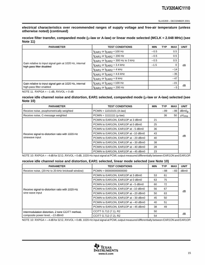
TYPICAL CHARACTERISTICS
0
5
10
15
20
25
30
35
40
45
–50 0 50 1000
5
10
15
20
25
30
–50 0 50 100
SUPPLY CURRENTvs
FREE-AIR TEMPERATURE(Detector OFF)
SUPPLY CURRENTvs
FREE-AIR TEMPERATURE(Detector ON)
DD
IS
up
ply
Cu
rren
t –
–A
µ
DD
IS
up
ply
Cu
rren
t –
–A
µ
TA – Free-Air Temperature – °C TA – Free-Air Temperature – °C
VDD = 3.3 V
VDD = 3.0 V
VDD = 3.3 V
VDD = 3.0 V
VDD = 2.7 V VDD = 2.7 V
–30
–25
–20
–15
–10
–5
0
5
100 1k
Rel
ativ
e G
ain
– d
B
–100
–80
–60
–40
–20
0
20
100 1k 10k
Rel
ativ
e G
ain
– d
B
RELATIVE GAINvs
FREQUENCY
RELATIVE GAINvs
FREQUENCY
f – Frequency – Hz f – Frequency – Hz
Both FiltersDisabled
High-PassFilter and
Slope FilterSelected
High-PassFilter Selected
and Slope FilterDisabled
Both FiltersDisabled
High-PassFilter Selectedand Slope FilterDisabled
High-PassFilter andSlope FilterSelected
Figure 10. Transmit Gain Response With Respect to Gain of 1-kHz Tone

TLV320AIC1110
SLAS359 – DECEMBER 2001
23www.ti.com
TYPICAL CHARACTERISTICS
–10
–15
–20
–25
10 100 1k 10k
Rel
ativ
e G
ain
– d
B–5
0
f – Frequency – Hz
RELATIVE GAIN RESPONSEvs
FREQUENCY
5
–30
–35
Figure 11. Receive Gain Response With Respect to Gain of 1-kHz Tone With High-Pass Filter Selected and High-Pass Filter Disabled

TLV320AIC1110
SLAS359 – DECEMBER 2001
24 www.ti.com
PRINCIPLES OF OPERATION
power-on initialization
An external reset with a minimum pulse width of 500 ns must be applied to the active low RESET terminal toassure reset upon power on. All registers are set with default values upon external reset initialization.
The desired selection for all programmable functions can be initialized prior to a power-up command using thecontrol interface.
Table 1. Power-Up and Power-Down Procedures (VDD = 2.7 V, earphone amplifier unloaded)
DEVICE STATUS PROCEDUREMAXIMUM POWER
CONSUMPTION
Power upSet bit 1 = 1 in power control register, EAR1 enabled 16.2 mW
Power upSet bit 1 = 0 in power control register, EAR2 enabled 14.6 mW
Power downSet bit 7 = 1 in TXPGA control register and bit 0 = 0 1.35 µW
Power downSet bit 7 = 0 in TXPGA control register and bit 0 = 0 67.5 µW
In addition to resetting the power down bit in the power control register, loss of MCLK (no transition detected)automatically enters the device into a power-down state with PCMO in the high impedance state. If during apulse code modulation (PCM) data transmit cycle an asynchronous power down occurs, the PCM interfaceremains powered up until the PCM data is completely transferred.
An additional power-down mode overrides the MCLK detection function. This allows the device to enter thepower down state without regard to MCLK. Setting bit 7 of the TXPGA sidetone register to logic high enablesthis function.
internal reference current setting terminal
Use a 100-kΩ precision resistor to connect the REXT pin to GND.
conversion laws
The device can be programmed for either a 15-bit linear or and 8-bit (µ-law or A-law) companding mode. Thecompanding operation approximates the CCITT G.711 recommendation. The linear mode operation uses a15-bit twos-complement format.
transmit operation
microphone input
The microphone input stage is a low-noise differential amplifier that provides a preamplifier gain of 23.5 dB. Itis recommended that a microphone capacitively connected to the MIC1N and MIC1P inputs, while the MIC2Nand MIC2P inputs can be used to capacitively connect a second microphone or an auxiliary audio circuit.

TLV320AIC1110
SLAS359 – DECEMBER 2001
25www.ti.com
PRINCIPLES OF OPERATION
transmit operation (continued)
_
+
_
+
Vref
510 kΩ
510 kΩ
34 kΩ
34 kΩ
Ci MIC1N
Ci MIC1P
MIC
Rmic
Rmic
MBIAS
Figure 12. Typical Microphone Interface
microphone mute function
Transmit channel muting provides 80-dB attenuation of the input microphone signal. The MICMUTE functioncan be selected by setting bit 6 of the power control register through the I2C interface.
transmit channel gain control
The values in the transmit PGA control registers control the gain in the transmit path. The total TX channel gaincan vary from 41.5 dB to 19.5 dB. The default total TX channel gain is 23.5 dB.
Table 2. Transmit Gain Control
BIT NAME MIC AMP1 MIC AMP2 TX PGAGAINMODE TOTAL TX GAIN
TP3 TP2 TP1 TP0 GAIN GAIN GAIN MIN TYP MAX UNIT
0 0 0 0 23.5 18 0 Extended 41.3 41.5 41.7 dB
0 0 0 1 23.5 18 –2 Extended 39.3 39.5 39.7 dB
0 0 1 0 23.5 18 –4 Extended 37.3 37.5 37.7 dB
0 0 1 1 23.5 18 –6 Extended 35.3 35.5 35.7 dB
0 1 0 0 23.5 18 –8 Extended 33.3 33.5 33.7 dB
0 1 0 1 23.5 18 –10 Extended 31.3 31.5 31.7 dB
1 0 0 0 23.5 6 0 Normal 29.3 29.5 29.7 dB
1 0 0 1 23.5 6 –2 Normal 27.3 27.5 27.7 dB
1 0 1 0 23.5 6 –4 Normal 25.3 25.5 25.7 dB
1 0 1 1 23.5 6 –6 Normal 23.3 23.5 23.7 dB
1 1 0 0 23.5 6 –8 Normal 21.3 21.5 21.7 dB
1 1 0 1 23.5 6 –10 Normal 19.3 19.5 19.7 dB

TLV320AIC1110
SLAS359 – DECEMBER 2001
26 www.ti.com
PRINCIPLES OF OPERATION
receive operation
receive channel gain control
The values in the receive PGA control registers control the gain in the receive path. PGA gain is set from – 6 dB to 6 dB in 1-dB steps through the I2C interface. The default receive channel gain is –4 dB.
Table 3. Receive PGA Gain Control
BIT NAME RELATIVE GAIN, VOICE MODEDTMF GAIN TONE NODE
RP3 RP2 RP1 RP0 MIN TYP MAX UNITDTMF GAIN, TONE NODE
0 0 0 0 5.8 6 6.2 dB 12
0 0 0 1 4.8 5 5.2 dB 12
0 0 1 0 3.8 4 4.2 dB 12
0 0 1 1 2.8 3 3.2 dB 6
0 1 0 0 1.8 2 2.2 dB 6
0 1 0 1 0.8 1 1.2 dB 6
0 1 1 0 –0.2 0 0.2 dB 0
0 1 1 1 –1.2 –1 –0.8 dB 0
1 0 0 0 –2.2 –2 –1.8 dB 0
1 0 0 1 –3.2 –3 –2.8 dB –6
1 0 1 0 –4.2 –4 –3.8 dB –6
1 0 1 1 –5.2 –5 –4.8 dB –6
1 1 0 0 –6.2 –6 –5.8 dB –12
1 1 0 1 X dB –12
1 1 1 0 X dB –12
sidetone gain control
The values in the sidetone PGA control registers control the sidetone gain. Sidetone gain is set from –12 dBto –24 dB in 2-dB steps through the I2C interface. Sidetone can be muted by setting bit 7 of the power controlregister. The default sidetone gain is –12 dB.
Table 4. Sidetone Gain Control
BIT NAME RELATIVE GAIN
ST2 ST1 ST0 MIN TYP MAX UNIT
0 0 0 –12.2 –12 –11.8 dB
0 0 1 –14.2 –14 –13.8 dB
0 1 0 –16.2 –16 –15.8 dB
0 1 1 –18.2 –18 –17.8 dB
1 0 0 –20.2 –20 –19.8 dB
1 0 1 –22.2 –22 –21.8 dB
1 1 0 –24.2 –24 –23.8 dB

TLV320AIC1110
SLAS359 – DECEMBER 2001
27www.ti.com
PRINCIPLES OF OPERATION
receive operation (continued)
receive volume control
The values in the volume control PGA control registers provide volume control for the earphone. Volume controlgain is set from 0 dB to –18 dB in 2-dB steps through the I2C interface. The default RX volume control gainis 0 dB.
Table 5. RX Volume Control
BIT NAME RELATIVE GAIN
RV3 RV2 RV1 RV0 MIN TYP MAX UNIT
0 0 0 0 –0.2 0 0.2 dB
0 0 0 1 –2.2 –2 –1.8 dB
0 0 1 0 –4.2 –4 –3.8 dB
0 0 1 1 –6.2 –6 –5.8 dB
0 1 0 0 –8.2 –8 –7.8 dB
0 1 0 1 –10.2 –10 –9.8 dB
0 1 1 0 –12.2 –12 –11.8 dB
0 1 1 1 –14.2 –14 –13.8 dB
1 0 0 0 –16.2 –16 –15.8 dB
1 0 0 1 –18.2 –18 –17.8 dB
earphone amplifier
The analog signal can be routed to either of two earphone amplifiers: one with a differential output (EAR1ONand EAR1OP) capable of driving a 8-Ω load, or one with a single-ended output (EAR2O) capable of driving a8-Ω load.
earphone mute function
Muting can be selected by setting bit 3 of the power control register through the I2C interface.
receive PCM data format
Companded mode: 8 bits are received, the most significant (MSB) first.
Linear mode: 15 bits are received, MSB first.

TLV320AIC1110
SLAS359 – DECEMBER 2001
28 www.ti.com
PRINCIPLES OF OPERATION
receive operation (continued)
Table 6. Receive-Data Bit Definitions
BIT NO. COMPANDEDMODE
LINEARMODE
1 CD7 LD14
2 CD6 LD13
3 CD5 LD12
4 CD4 LD11
5 CD3 LD10
6 CD2 LD9
7 CD1 LD8
8 CD0 LD7
9 – LD6
10 – LD5
11 – LD4
12 – LD3
13 – LD2
14 – LD1
15 – LD0
16 – ––
Transmit channel gain control bits always follow the PCM data in time:
CD7-CD0 = data word in companded mode
LD14-LD0 = data word in linear mode
DTMF generator operation and interface
The DTMF circuit generates the summed DTMF tones for push button dialing and provides the PDM output forthe BUZZCON user-alert tone. The integer value is determined by the formula round tone [Freq (Hz)/resolution(Hz)]. The integer value is loaded into one of two 8-bit registers, high-tone register (04) or low-tone register (05).The tone output is 2 dB higher when applied to the high-tone register (04). When generating DTMF tones, thehigh-frequency value must be applied to the high tone register (04) and the low DTMF value to the low-toneregister.
The DTMF frequency resolution is controlled by the auxiliary register (06) bits 2, 3, 4, and 5. When the resolutionis set to 7.8125 Hz, the frequency range can be up to 1992.2 Hz. A wider range can be accomplished (forexample, 2x or 4x) by selecting lower resolutions of 15.625 Hz or 31.250 Hz. The gain setting is controlled bythe RXPGA gain control. This register applies the required gain to obtain MUX control during tone modeoperation. Table 3 shows the relationship of the two gain settings.

TLV320AIC1110
SLAS359 – DECEMBER 2001
29www.ti.com
PRINCIPLES OF OPERATION
DTMF generator operation and interface (continued)
Table 7. Typical DTMF and Single Tone Control
DT7 DT6 DT5 DT4 DT3 DT2 DT1 DT0INTEGER
VALUETONE
FUNCTION TONE/HZ
0 1 0 1 1 0 0 1 89 DTMF Low 697
0 1 1 0 0 0 1 1 99 DTMF Low 770
0 1 1 0 1 1 0 1 109 DTMF Low 852
0 1 1 1 1 0 0 0 120 DTMF Low 941
1 0 0 1 1 0 1 1 155 DTMF HIgh 1209
1 0 1 0 1 0 1 1 171 DTMF HIgh 1336
1 0 1 1 1 1 0 1 189 DTMF HIgh 1477
1 1 0 1 0 0 0 1 209 DTMF HIgh 1633
Tones from the DTMF generator block are present at all outputs and are controlled by enabling or disabling theindividual output ports. The values that determine the tone frequency are loaded into the tone registers (highand low) as two separate values.
The values loaded into the tone registers initiate an iterative table look-up function, placing a 6-bit or 7-bit intwos-complement value into the the tone registers. There is a 2-dB difference in the resulting output of the tworegisters, the high-tone register having the greater result.
In the case of low-tone signal, the tone generator outputs a 6-bit integer with a maximum code of 31 (011111).However, the DTMF output is an 8-bit integer. Therefore, two zeros are padded to the MSB position, whichresults in 31 (00011111). On the other hand, the receive channel requires a 15-bit integer, the input 3968(000111110000000). Since the maximum digital value of receive channel is 16383 (011111111111111), themaximum low-tone signal is designed to be –12.32 dB below the full digital scale.
20 log 396816383
2 –12.32 dB
In the case of high-tone signal, the tone generator outputs a 7-bit integer with a maximum code of 39 (0100111).The DTMF, therefore, pads a zero to the MSB and generates an 8-bit integer (00100111). In order to send thedigital code to receive channel, it is converted to a 15-bit integer with seven more zeros padded to LSB positionand biased as 4992 (001001110000000). Therefore, the maximum high-tone signal is designed to be –10.32 dBbelow the full digital scale.
20 log 499216383
2 –10.32 dB
In the case of DTMF output, the tone generator outputs an 8-bit integer with the maximum code level of 70(01000110). This output is converted to a 15-bit code with the value of 8960 (010001100000000). Therefore,the maximum output of DTMF is designed to be –5.24 dB below the full digital scale.
20 log 896016383
2 –5.24 dB
(1)
(2)
(3)

TLV320AIC1110
SLAS359 – DECEMBER 2001
30 www.ti.com
PRINCIPLES OF OPERATION
buzzer logic section
The single-ended output BUZZCON is a PDM signal intended to drive a buzzer through an external drivertransistor. The PDM begins as a selected DTMF tone, generated and passed through the receive D/A channeland fed back to the transmit channel analog modulator, where a PDM signal is generated and routed to theBUZZCON output.
Buzzcon
DTMFDTMFGainMux
DigitalModulator
andFilter
AnalogModulator
BuzzerControl
Figure 13. Buzzer Driver System Architecture
support section
The clock generator and control circuit use the master clock input (MCLK) to generate internal clocks to driveinternal counters, filters, and convertors. Register control data is written into and read back from the PCM codecregisters via the control interface.
I2C-bus protocols
The PCM codec serial interface is designed to be I2C bus-compatible and operates in the slave mode when CEis high. This interface consists of the following terminals:
SCL: I2C-bus serial clock. This input synchronizes the control data transfer to and from the codec.
SDA: I2C-bus serial address/data input/output. This is a bidirectional terminal that transfers registercontrol addresses and data into and out of the codec. It is an open drain terminal and thereforerequires a pullup resistor to VCC (typical 10 kΩ for 100 kHz).
TLV320AIC1110 has a fixed device select address of (E2)HEX for write mode and (E3)HEX for read mode.
For normal data transfer, SDA is allowed to change only when SCL is low. Changes when SCL is high arereserved for indicating the start and stop conditions.
Data transfer may be initiated only when the bus is not busy. During data transfer, the data line must remainstable whenever the clock line is at high. Changes in the data line while the clock line is at high are interpretedas a start or stop condition.
Table 8. I2C-Bus Conditions
CONDITION STATUS DESCRIPTION
A Bus not busy Both data and clock lines remain at high.
B Start data transferA high to low transition of the SDA line while the clock (SCL) is high determines a start condition.All commands must proceed from a start condition.
C Stop data transferA low to high transition of the SDA line while the clock (SCL) is high determines a stop condition.All operations must end with a stop condition.
D Data validThe state of the data line represents valid data when, after a start condition, the data line is stablefor the duration of the high period of the clock signal.
The data on the line must be changed during the low period of the clock signal. There is one clock pulse perbit of data.
TLV320AIC1110
SLAS359 – DECEMBER 2001
31www.ti.com
PRINCIPLES OF OPERATION
I2C-bus protocols (continued)
Each data transfer is initiated with a start condition and terminated with a stop condition. The number of databytes, transferred between the start and stop conditions, is determined by the master device (microprocessor).
When addressed, the PCM codec generates an acknowledge after the reception of each byte. The masterdevice must generate an extra clock pulse that is associated with this acknowledge bit.
The PCM codec must pull down the SDA line during the acknowledge clock pulse so that the SDA line is at stablelow state during the high period of the acknowledge related clock pulse. Setup and hold times must be takeninto account. During read operations, the master device must signal an end of data to the slave by not generatingan acknowledge bit on the last byte that was clocked out of the slave. In this case, the slave (PCM codec) mustleave the data line high to enable the master device to generate the stop condition.
clock frequencies and sample rates
A fixed PCMSYN rate of 8 kHz determines the sampling rate.
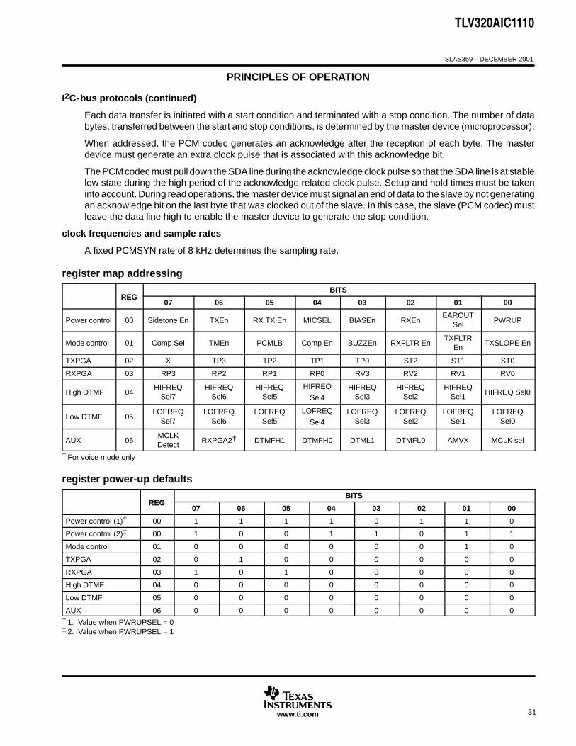
register map addressing
REGBITS
REG07 06 05 04 03 02 01 00
Power control 00 Sidetone En TXEn RX TX En MICSEL BIASEn RXEnEAROUT
SelPWRUP
Mode control 01 Comp Sel TMEn PCMLB Comp En BUZZEn RXFLTR EnTXFLTR
EnTXSLOPE En
TXPGA 02 X TP3 TP2 TP1 TP0 ST2 ST1 ST0
RXPGA 03 RP3 RP2 RP1 RP0 RV3 RV2 RV1 RV0
High DTMF 04HIFREQ
Sel7HIFREQ
Sel6HIFREQ
Sel5HIFREQ
Sel4HIFREQ
Sel3HIFREQ
Sel2HIFREQ
Sel1HIFREQ Sel0
Low DTMF 05LOFREQ
Sel7LOFREQ
Sel6LOFREQ
Sel5LOFREQ
Sel4LOFREQ
Sel3LOFREQ
Sel2LOFREQ
Sel1LOFREQ
Sel0
AUX 06MCLKDetect
RXPGA2† DTMFH1 DTMFH0 DTML1 DTMFL0 AMVX MCLK sel
† For voice mode only
register power-up defaults
REGBITS
REG07 06 05 04 03 02 01 00
Power control (1)† 00 1 1 1 1 0 1 1 0
Power control (2)‡ 00 1 0 0 1 1 0 1 1
Mode control 01 0 0 0 0 0 0 1 0
TXPGA 02 0 1 0 0 0 0 0 0
RXPGA 03 1 0 1 0 0 0 0 0
High DTMF 04 0 0 0 0 0 0 0 0
Low DTMF 05 0 0 0 0 0 0 0 0
AUX 06 0 0 0 0 0 0 0 0† 1. Value when PWRUPSEL = 0‡ 2. Value when PWRUPSEL = 1
TLV320AIC1110
SLAS359 – DECEMBER 2001
32 www.ti.com
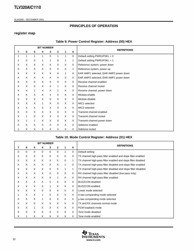
PRINCIPLES OF OPERATION
register map
Table 9. Power Control Register: Address (00) HEX
BIT NUMBERDEFINITIONS
7 6 5 4 3 2 1 0DEFINITIONS
1 1 1 1 0 1 1 0 Default setting PWRUPSEL = 0
1 0 0 1 1 0 1 1 Default setting PWRUPSEL = 1
X X X X X X X 0 Reference system, power down
X X X X X X X 1 Reference system, power up
X X X X X X 1 X EAR AMP1 selected, EAR AMP2 power down
X X X X X X 0 X EAR AMP2 selected, EAR AMP1 power down
X X X X X 0 X X Receive channel enabled
X X 0 X X 1 X X Receive channel muted
X X 1 X X 1 X 0 Receive channel, power down
X X X X 1 X X X Micbias enable
X X X X 0 X X X Micbias disable
X X X 1 X X X X MIC1 selected
X X X 0 X X X X MIC2 selected
X 0 X X X X X X Transmit channel enabled
X 1 0 X X X X X Transmit channel muted
X 1 1 X X X X X Transmit channel power down
0 X X X X X X X Sidetone enabled
1 X X X X X X X Sidetone muted
Table 10. Mode Control Register: Address (01) HEX
BIT NUMBERDEFINITIONS
7 6 5 4 3 2 1 0DEFINITIONS
0 0 0 0 0 0 1 0 Default setting
X X X X X X 0 0 TX channel high-pass filter enabled and slope filter enabled
X X X X X X 0 1 TX channel high-pass filter enabled and slope filter disabled
X X X X X X 1 0 TX channel high-pass filter disabled and slope filter enabled
X X X X X X 1 1 TX channel high-pass filter disabled and slope filter disabled
X X X X X 0 X X RX channel high-pass filter disabled (low pass only)
X X X X X 1 X X RX channel high-pass filter enabled
X X X X 0 X X X BUZZCON disabled
X X X X 1 X X X BUZZCON enabled
X X X 0 X X X X Linear mode selected
1 X X 1 X X X X A-law companding mode selected
0 X X 1 X X X X µ-law companding mode selected
X X 0 X X X X X TX and RX channels normal mode
X X 1 X X X X X PCM loopback mode
X 0 X X X X X X Tone mode disabled
X 1 X X X X X X Tone mode enabled

TLV320AIC1110
SLAS359 – DECEMBER 2001
33www.ti.com
PRINCIPLES OF OPERATION
register map (continued)
Transmit PGA and sidetone control register: Address (02)HEX
Bit definitions:
7 6 5 4 3 2 1 0 DEFINITION
X TP3 TP2 TP1 TP0 ST2 ST1 ST0 See Table 2 and Table 4
0 1 0 0 0 0 0 0 Default setting
Receive volume control register: Address (03)HEX
Bit definitions:
7 6 5 4 3 2 1 0 DEFINITION
RP3 RP2 RP1 RP0 RV3 RV2 RV1 RV0 See Table 3 and Table 5
1 0 1 0 0 0 0 0 Default setting
High tone selection control register: Address (04)HEX
Bit definitions:
7 6 5 4 3 2 1 0 DEFINITION
X X X X X X X X DTMF (see Table 7)
0 0 0 0 0 0 0 0 Default setting
Low tone selection control register: Address (05)HEX
Bit definitions :
7 6 5 4 3 2 1 0 DEFINITION
X X X X X X X X DTMF (see Table 7)
0 0 0 0 0 0 0 0 Default setting
Auxiliary register: Address (06)HEX
Bit definitions:
7 6 5 4 3 2 1 0 DEFINITION
0 0 0 0 0 0 0 0 Default
X X X X X X X 0 MCLK is set to 2.048 MHz
X X X X X X X 1 MCLK is set to 128 MHz
X X X X X X 0 X Analog switch output is set to OUT2
X X X X X X 1 X Analog switch output is set to OUT1
X X X X 0 0 X X Low tone frequency resolution is set to 7.8125 Hz
X X X X 0 1 X X Low tone frequency resolution is set to 15.625 Hz
X X X X 1 0 X X Low tone frequency resolution is set to 31.250 Hz
X X 0 0 X X X X High tone frequency resolution is set to 7.8125 Hz
X X 0 1 X X X X High tone frequency resolution is set to 15.625 Hz
X X 1 0 X X X X High tone frequency resolution is set to 31.250 Hz
X 0 X X X X X X Receiver channel gain, RXPGA2 is equal to 0 dB, voice mode only
X 1 X X X X X X Receiver channel gain, RXPGA2 is equal to 6 dB, voice mode only
0 X X X X X X X MCLK detector is powered ON
1 X X X X X X X MCLK detector is powered OFF

TLV320AIC1110
SLAS359 – DECEMBER 2001
34 www.ti.com
PRINCIPLES OF OPERATION
using PCM codec as a general-purpose PCM codec
In situations when a general-purpose PCM codec is needed and programming features are not necessary, thereceive and transmit channels can be enabled for voice mode only by setting the powerup select pin to VCC level.
When set to default, the following features are activated:
REF is powered up
Ear amp1 selected, Ear amp 2 = OFF
Receive channel enabled
MIC bias enabled
MIC 2 selected
Transmit channel enabled
Side tone enabled, Gain = –12 dB
TX channel high pass filter disabled
TX channel slope filter enabled
RX channel HP filter disabled (low pass only)
Buzzcon disabled
Linear mode only
TX and RX channel normal mode (no loopback)
Tone mode disabled (voice mode only)
MIC amp 1 gain = 23.5 dBMIC amp 2 gain = 6 dBTX PGA gain = 0 dBTotal TX gain = 29.5 dB
Receive PGA = –4 dBReceive PGA 2 = 0 dBVolume = 0 dBTotal RX gain = –4 dB
Clock = 2.048 MHz

TLV320AIC1110
SLAS359 – DECEMBER 2001
35www.ti.com
PRINCIPLES OF OPERATION
PCM codec device comparisons
TLV320AIC1103 TLV320AIC1110
Single tone frequency range To 2 kHz To 8 kHz
Transmit channel gain range 13.5 dB to 35.5 dB 19.5 dB to 41.5 dB
Receive channel gain range – 24 dB to 6 dB – 24 dB to 12 dB
PCMCLK rate 2.048 MHz 128 kHz or 2.048 MHz
Device pin out Backward compatible (TQFP)
Control registers Backward compatible
Number of registers 6 7
Control interface I2C I2C
Analog switch No Yes
Earout driving impedance 32 Ω 8-32 Ω
DTMF Yes Yes
Tone resolution (Hz) 7.81257.812515.62531.25
Packages TQFP TQFP,MicroStar Junior BGA

PACKAGE OPTION ADDENDUM
www.ti.com 10-Jun-2014
Addendum-Page 1
PACKAGING INFORMATION
Orderable Device Status(1)
Package Type PackageDrawing
Pins PackageQty
Eco Plan(2)
Lead/Ball Finish(6)
MSL Peak Temp(3)
Op Temp (°C) Device Marking(4/5)
Samples
TLV320AIC1110GQER LIFEBUY BGAMICROSTAR
JUNIOR
GQE 80 TBD Call TI Call TI -40 to 85 AIC1110
TLV320AIC1110PBS ACTIVE TQFP PBS 32 250 Green (RoHS& no Sb/Br)
CU NIPDAU Level-3-260C-168 HR -40 to 85 AIC1110
TLV320AIC1110PBSG4 ACTIVE TQFP PBS 32 250 Green (RoHS& no Sb/Br)
CU NIPDAU Level-3-260C-168 HR -40 to 85 AIC1110
TLV320AIC1110PBSR ACTIVE TQFP PBS 32 1000 Green (RoHS& no Sb/Br)
CU NIPDAU Level-3-260C-168 HR -40 to 85 AIC1110
TLV320AIC1110ZQER ACTIVE BGAMICROSTAR
JUNIOR
ZQE 80 2500 Green (RoHS& no Sb/Br)
SNAGCU Level-3-260C-168 HR -40 to 85 AIC1110
(1) The marketing status values are defined as follows:ACTIVE: Product device recommended for new designs.LIFEBUY: TI has announced that the device will be discontinued, and a lifetime-buy period is in effect.NRND: Not recommended for new designs. Device is in production to support existing customers, but TI does not recommend using this part in a new design.PREVIEW: Device has been announced but is not in production. Samples may or may not be available.OBSOLETE: TI has discontinued the production of the device.
(2) Eco Plan - The planned eco-friendly classification: Pb-Free (RoHS), Pb-Free (RoHS Exempt), or Green (RoHS & no Sb/Br) - please check http://www.ti.com/productcontent for the latest availabilityinformation and additional product content details.TBD: The Pb-Free/Green conversion plan has not been defined.Pb-Free (RoHS): TI's terms "Lead-Free" or "Pb-Free" mean semiconductor products that are compatible with the current RoHS requirements for all 6 substances, including the requirement thatlead not exceed 0.1% by weight in homogeneous materials. Where designed to be soldered at high temperatures, TI Pb-Free products are suitable for use in specified lead-free processes.Pb-Free (RoHS Exempt): This component has a RoHS exemption for either 1) lead-based flip-chip solder bumps used between the die and package, or 2) lead-based die adhesive used betweenthe die and leadframe. The component is otherwise considered Pb-Free (RoHS compatible) as defined above.Green (RoHS & no Sb/Br): TI defines "Green" to mean Pb-Free (RoHS compatible), and free of Bromine (Br) and Antimony (Sb) based flame retardants (Br or Sb do not exceed 0.1% by weightin homogeneous material)
(3) MSL, Peak Temp. - The Moisture Sensitivity Level rating according to the JEDEC industry standard classifications, and peak solder temperature.
(4) There may be additional marking, which relates to the logo, the lot trace code information, or the environmental category on the device.
(5) Multiple Device Markings will be inside parentheses. Only one Device Marking contained in parentheses and separated by a "~" will appear on a device. If a line is indented then it is a continuationof the previous line and the two combined represent the entire Device Marking for that device.

PACKAGE OPTION ADDENDUM
www.ti.com 10-Jun-2014
Addendum-Page 2
(6) Lead/Ball Finish - Orderable Devices may have multiple material finish options. Finish options are separated by a vertical ruled line. Lead/Ball Finish values may wrap to two lines if the finishvalue exceeds the maximum column width.
Important Information and Disclaimer:The information provided on this page represents TI's knowledge and belief as of the date that it is provided. TI bases its knowledge and belief on informationprovided by third parties, and makes no representation or warranty as to the accuracy of such information. Efforts are underway to better integrate information from third parties. TI has taken andcontinues to take reasonable steps to provide representative and accurate information but may not have conducted destructive testing or chemical analysis on incoming materials and chemicals.TI and TI suppliers consider certain information to be proprietary, and thus CAS numbers and other limited information may not be available for release.
In no event shall TI's liability arising out of such information exceed the total purchase price of the TI part(s) at issue in this document sold by TI to Customer on an annual basis.

TAPE AND REEL INFORMATION
*All dimensions are nominal
Device PackageType
PackageDrawing
Pins SPQ ReelDiameter
(mm)
ReelWidth
W1 (mm)
A0(mm)
B0(mm)
K0(mm)
P1(mm)
W(mm)
Pin1Quadrant
TLV320AIC1110PBSR TQFP PBS 32 1000 330.0 16.4 7.2 7.2 1.5 12.0 16.0 Q2
TLV320AIC1110ZQER BGA MI CROSTA
R JUNI OR
ZQE 80 2500 330.0 12.4 5.3 5.3 1.5 8.0 12.0 Q1
PACKAGE MATERIALS INFORMATION
www.ti.com 10-Oct-2012
Pack Materials-Page 1

*All dimensions are nominal
Device Package Type Package Drawing Pins SPQ Length (mm) Width (mm) Height (mm)
TLV320AIC1110PBSR TQFP PBS 32 1000 367.0 367.0 38.0
TLV320AIC1110ZQER BGA MICROSTARJUNIOR
ZQE 80 2500 338.1 338.1 20.6
PACKAGE MATERIALS INFORMATION
www.ti.com 10-Oct-2012
Pack Materials-Page 2

IMPORTANT NOTICETexas Instruments Incorporated and its subsidiaries (TI) reserve the right to make corrections, enhancements, improvements and otherchanges to its semiconductor products and services per JESD46, latest issue, and to discontinue any product or service per JESD48, latestissue. Buyers should obtain the latest relevant information before placing orders and should verify that such information is current andcomplete. All semiconductor products (also referred to herein as “components”) are sold subject to TI’s terms and conditions of salesupplied at the time of order acknowledgment.TI warrants performance of its components to the specifications applicable at the time of sale, in accordance with the warranty in TI’s termsand conditions of sale of semiconductor products. Testing and other quality control techniques are used to the extent TI deems necessaryto support this warranty. Except where mandated by applicable law, testing of all parameters of each component is not necessarilyperformed.TI assumes no liability for applications assistance or the design of Buyers’ products. Buyers are responsible for their products andapplications using TI components. To minimize the risks associated with Buyers’ products and applications, Buyers should provideadequate design and operating safeguards.TI does not warrant or represent that any license, either express or implied, is granted under any patent right, copyright, mask work right, orother intellectual property right relating to any combination, machine, or process in which TI components or services are used. Informationpublished by TI regarding third-party products or services does not constitute a license to use such products or services or a warranty orendorsement thereof. Use of such information may require a license from a third party under the patents or other intellectual property of thethird party, or a license from TI under the patents or other intellectual property of TI.Reproduction of significant portions of TI information in TI data books or data sheets is permissible only if reproduction is without alterationand is accompanied by all associated warranties, conditions, limitations, and notices. TI is not responsible or liable for such altereddocumentation. Information of third parties may be subject to additional restrictions.Resale of TI components or services with statements different from or beyond the parameters stated by TI for that component or servicevoids all express and any implied warranties for the associated TI component or service and is an unfair and deceptive business practice.TI is not responsible or liable for any such statements.Buyer acknowledges and agrees that it is solely responsible for compliance with all legal, regulatory and safety-related requirementsconcerning its products, and any use of TI components in its applications, notwithstanding any applications-related information or supportthat may be provided by TI. Buyer represents and agrees that it has all the necessary expertise to create and implement safeguards whichanticipate dangerous consequences of failures, monitor failures and their consequences, lessen the likelihood of failures that might causeharm and take appropriate remedial actions. Buyer will fully indemnify TI and its representatives against any damages arising out of the useof any TI components in safety-critical applications.In some cases, TI components may be promoted specifically to facilitate safety-related applications. With such components, TI’s goal is tohelp enable customers to design and create their own end-product solutions that meet applicable functional safety standards andrequirements. Nonetheless, such components are subject to these terms.No TI components are authorized for use in FDA Class III (or similar life-critical medical equipment) unless authorized officers of the partieshave executed a special agreement specifically governing such use.Only those TI components which TI has specifically designated as military grade or “enhanced plastic” are designed and intended for use inmilitary/aerospace applications or environments. Buyer acknowledges and agrees that any military or aerospace use of TI componentswhich have not been so designated is solely at the Buyer's risk, and that Buyer is solely responsible for compliance with all legal andregulatory requirements in connection with such use.TI has specifically designated certain components as meeting ISO/TS16949 requirements, mainly for automotive use. In any case of use ofnon-designated products, TI will not be responsible for any failure to meet ISO/TS16949.Products ApplicationsAudio www.ti.com/audio Automotive and Transportation www.ti.com/automotiveAmplifiers amplifier.ti.com Communications and Telecom www.ti.com/communicationsData Converters dataconverter.ti.com Computers and Peripherals www.ti.com/computersDLP® Products www.dlp.com Consumer Electronics www.ti.com/consumer-appsDSP dsp.ti.com Energy and Lighting www.ti.com/energyClocks and Timers www.ti.com/clocks Industrial www.ti.com/industrialInterface interface.ti.com Medical www.ti.com/medicalLogic logic.ti.com Security www.ti.com/securityPower Mgmt power.ti.com Space, Avionics and Defense www.ti.com/space-avionics-defenseMicrocontrollers microcontroller.ti.com Video and Imaging www.ti.com/videoRFID www.ti-rfid.comOMAP Applications Processors www.ti.com/omap TI E2E Community e2e.ti.comWireless Connectivity www.ti.com/wirelessconnectivity
Mailing Address: Texas Instruments, Post Office Box 655303, Dallas, Texas 75265Copyright © 2014, Texas Instruments Incorporated