
LNICST 154 - Implementation of DVB-S2X Super-Frame Format ...

HUAWEI LGA Module
PCM Audio Design Guide
Issue 04
Date 2016-12-12
Copyright © Huawei Technologies Co., Ltd. 2016. All rights reserved.
No part of this manual may be reproduced or transmitted in any form or by any means without prior written
consent of Huawei Technologies Co., Ltd. and its affiliates ("Huawei").
The product described in this manual may include copyrighted software of Huawei and possible licensors.
Customers shall not in any manner reproduce, distribute, modify, decompile, disassemble, decrypt, extract,
reverse engineer, lease, assign, or sublicense the said software, unless such restrictions are prohibited by
applicable laws or such actions are approved by respective copyright holders.
Trademarks and Permissions
, , and are trademarks or registered trademarks of Huawei Technologies Co., Ltd.
Other trademarks, product, service and company names mentioned may be the property of their respective
owners.
Notice
Some features of the product and its accessories described herein rely on the software installed, capacities
and settings of local network, and therefore may not be activated or may be limited by local network
operators or network service providers.
Thus, the descriptions herein may not exactly match the product or its accessories which you purchase.
Huawei reserves the right to change or modify any information or specifications contained in this manual
without prior notice and without any liability.
DISCLAIMER
ALL CONTENTS OF THIS MANUAL ARE PROVIDED “AS IS”. EXCEPT AS REQUIRED BY APPLICABLE
LAWS, NO WARRANTIES OF ANY KIND, EITHER EXPRESS OR IMPLIED, INCLUDING BUT NOT
LIMITED TO, THE IMPLIED WARRANTIES OF MERCHANTABILITY AND FITNESS FOR A PARTICULAR
PURPOSE, ARE MADE IN RELATION TO THE ACCURACY, RELIABILITY OR CONTENTS OF THIS
MANUAL.
TO THE MAXIMUM EXTENT PERMITTED BY APPLICABLE LAW, IN NO EVENT SHALL HUAWEI BE
LIABLE FOR ANY SPECIAL, INCIDENTAL, INDIRECT, OR CONSEQUENTIAL DAMAGES, OR LOSS OF
PROFITS, BUSINESS, REVENUE, DATA, GOODWILL SAVINGS OR ANTICIPATED SAVINGS
REGARDLESS OF WHETHER SUCH LOSSES ARE FORSEEABLE OR NOT.
THE MAXIMUM LIABILITY (THIS LIMITATION SHALL NOT APPLY TO LIABILITY FOR PERSONAL
INJURY TO THE EXTENT APPLICABLE LAW PROHIBITS SUCH A LIMITATION) OF HUAWEI ARISING
FROM THE USE OF THE PRODUCT DESCRIBED IN THIS MANUAL SHALL BE LIMITED TO THE
AMOUNT PAID BY CUSTOMERS FOR THE PURCHASE OF THIS PRODUCT.
Import and Export Regulations
Customers shall comply with all applicable export or import laws and regulations and be responsible to
obtain all necessary governmental permits and licenses in order to export, re-export or import the product
mentioned in this manual including the software and technical data therein.
Privacy Policy
To better understand how we protect your personal information, please see the privacy policy at
http://consumer.huawei.com/privacy-policy.
HUAWEI LGA Module PCM Audio Design Guide About This Document
Issue 04 (2016-12-12) Huawei Proprietary and Confidential
Copyright © Huawei Technologies Co., Ltd. 3
About This Document
Revision History
Document Version
Date Chapter Descriptions
01 2011-05-04 Creation
02 2015-02-10 2 Updated chapter 2 PCM Interface
3 Deleted chapter 3 Timing in issue 01
3 Updated chapter 3 Reference Design
5 Deleted chapter 5 Audio Application of PCM in issue 01
03 2015-08-06 3.1 Deleted the description about TLV320AIC1106
3.2.1 Deleted the chapter of TLV320AIC1106
04 2016-12-12 All Deleted the description related to MU609
Scope MU509 series
MC509 series
MU709 series
ME909u-521

HUAWEI LGA Module PCM Audio Design Guide Contents
Issue 04 (2016-12-12) Huawei Proprietary and Confidential
Copyright © Huawei Technologies Co., Ltd. 4
Contents
1 Introduction ........................................................................................................................... 5
2 PCM Interface ........................................................................................................................ 6
2.1 Definitions of Pins ........................................................................................................................... 6
2.2 Configuration Modes ....................................................................................................................... 6
2.2.1 PCM Working Mode................................................................................................................ 6
2.2.2 PCM Data Format ................................................................................................................... 7
2.2.3 PCM Clock Signal ................................................................................................................... 7
2.2.4 PCM SYNC Frame Format ..................................................................................................... 8
2.2.5 PCM Offset Setting ................................................................................................................. 9
2.2.6 PCM DATA Polarity ................................................................................................................. 9
2.2.7 PCM DATA Length ................................................................................................................ 10
2.2.8 PCM SYNC Frequency ......................................................................................................... 10
2.2.9 PCM Master Output Data Format ......................................................................................... 10
3 Reference Design ................................................................................................................. 12
3.1 System Block ................................................................................................................................ 12
3.2 Reference Schematic and Software Configuration........................................................................ 13
3.2.1 TLV320AIC3204 ................................................................................................................... 13
3.2.2 NAU8814 .............................................................................................................................. 16
HUAWEI LGA Module PCM Audio Design Guide Introduction
Issue 04 (2016-12-12) Huawei Proprietary and Confidential
Copyright © Huawei Technologies Co., Ltd. 5
1 Introduction
The purpose of this document is to describe some hardware specification which is useful to develop a product with Huawei LGA module supporting PCM (Pulse-Coded Modulation). This document is intended for customers who are integrators and about to implement their applications by using Huawei LGA module.
Huawei LGA module supports the PCM, which can be used for the module to
transmit and receive digital audio data, and uses the PCM interface as part of the audio front end; therefore an external codec is easily allowed to be used instead of the internal codec. For example, through the PCM you could connect Huawei LGA module to a Bluetooth device.
Huawei LGA module has one PCM port. Please refer to the hardware guide of the
module that you are in use to know the pin number of the PCM port.

HUAWEI LGA Module PCM Audio Design Guide PCM Interface
Issue 04 (2016-12-12) Huawei Proprietary and Confidential
Copyright © Huawei Technologies Co., Ltd. 6
2 PCM Interface
2.1 Definitions of Pins Definitions of pins on the PCM interface of Huawei LGA module is as shown in Table 2-1 .
Table 2-1 Definitions of pins on the PCM interface
Pin No. Pin Name I/O Description
Normal MUX
5 PCM_SYNC GPIO I/O PCM interface sync
6 PCM_DIN GPIO I PCM I/F data in
7 PCM_DOUT GPIO O PCM I/F data out
8 PCM_CLK GPIO I/O PCM interface clock
When Huawei LGA module works on the master mode, PCM_CLK and PCM_SYNC pins
are in the output status; when it works on the slave mode, PCM_CLK and PCM_SYNC pins are in the input status.
Each module has two editions: Data only or Telematics. Data only does not support the PCM function.
Following configurations in section 2.2 , except PCM data polarity, can be modified by AT^CPCM command.
2.2 Configuration Modes
2.2.1 PCM Working Mode
Huawei LGA module supports three PCM working modes, including MASTER_PRIM mode, MASTER_AUX mode and SLAVE mode.

HUAWEI LGA Module PCM Audio Design Guide PCM Interface
Issue 04 (2016-12-12) Huawei Proprietary and Confidential
Copyright © Huawei Technologies Co., Ltd. 7
PCM working mode Description
MASTER_PRIM mode In this mode, the PCM_CLK and PCM_SYNC signal clocks are generated by the module. And the frame format is short frame.
MASTER_AUX mode In this mode, the PCM_CLK and PCM_SYNC signal clocks are generated by the module. And the frame format is long frame.
SLAVE mode In this mode, the PCM_CLK and PCM_SYNC signal
clocks are generated by the external CODEC chip.
Each module supports different PCM working modes, as shown in Table 2-2 .
Table 2-2 PCM working modes supported by different modules
Module MASTER_PRIM mode MASTER_AUX mode SLAVE mode
MU509 series Support (default) Not support Not support
MC509 series Support (default) Not support Not support
MU709 series Support (default) Not support Support
ME909u-521 Support (default) Not support Not support
2.2.2 PCM Data Format
Huawei LGA module supports three PCM data formats, including Linear, u-law and
A-law. And each module supports different PCM data formats, as shown in Table 2-3 .
Table 2-3 PCM data formats supported by different modules
Module Linear u-law A-law
MU509 series Support (default) Support Not support
MC509 series Support (default) Support Not support
MU709 series Support (default) Not support Not support
ME909u-521 Support (default) Not support Not support
2.2.3 PCM Clock Signal
In MASTER_PRIM mode, the PCM bit clock supported by Huawei LGA module is 2.048 MHz only, except ME909u-521 also supports 4.096 MHz, as shown in Table 2-4 .

HUAWEI LGA Module PCM Audio Design Guide PCM Interface
Issue 04 (2016-12-12) Huawei Proprietary and Confidential
Copyright © Huawei Technologies Co., Ltd. 8
Table 2-4 PCM bit clocks supported by different modules in MASTER_PRIM mode
Module 2.048 Mhz 1.024 MHz 512 kHz 256 kHz 4.096 MHz
MU509
series
Support (default)
Not support Not support Not support Not support
MC509
series
Support
(default)
Not support Not support Not support Not support
MU709
series
Support (default)
Not support Not support Not support Not support
ME909u-521
Support (default)
Not support Not support Not support Support
2.2.4 PCM SYNC Frame Format
PCM_SYNC supports long frame format and short frame format.
Short frame: PCM_SYNC only keeps one clock time high.
Long frame: PCM_SYNC keeps more than one clock time high.
The two timing sequences above are not real, but used to describe the short and long frames.
Table 2-5 PCM SYNC frame formats supported by different modules
Module Short frame Long frame
MU509 series Support (default) Not support
MC509 series Support (default) Not support
MU709 series Support (default) Not support
ME909u-521 Support (default) Not support

HUAWEI LGA Module PCM Audio Design Guide PCM Interface
Issue 04 (2016-12-12) Huawei Proprietary and Confidential
Copyright © Huawei Technologies Co., Ltd. 9
2.2.5 PCM Offset Setting
Huawei LGA module supports three PCM offset settings, including offset cleared, short sync offset set and long sync offset set.
PCM offset setting Description
Offset cleared The sync launched is aligned to the rising edge of the PCM_CLK.
Short sync offset set The short sync sent to the external world in MASTER_PRIM mode is launched 1/4 cycle after the rising edge of the PCM_CLK.
Long sync offset set The long sync sent to the external world in MASTER_AUX mode is launched 1/4 cycle ahead of the rising edge of PCM_CLK.
Table 2-6 PCM offset settings supported by different modules
Module Offset cleared Short sync offset set Long sync offset set
MU509 series Support (default) Support Not support
MC509 series Support (default) Support Not support
MU709 series Support (default) Not support Not support
ME909u-521 Support (default) Not support Not support
2.2.6 PCM DATA Polarity
Huawei LGA module supports two PCM data polarity settings, including falling edge and rising edge.
PCM data polarity Description
Falling edge The data input or output is followed the falling edge of PCM_CLK.
Rising edge The data input or output is followed the rising edge of PCM_CLK.
Each module supports different PCM data polarity settings, as shown in Table 2-7 . And the setting cannot be modified by AT^CPCM command.
Table 2-7 PCM data polarity settings supported by different modules
Module Falling edge Rising edge
MU509 series Support (default) Not support
HUAWEI LGA Module PCM Audio Design Guide PCM Interface
Issue 04 (2016-12-12) Huawei Proprietary and Confidential
Copyright © Huawei Technologies Co., Ltd. 10
Module Falling edge Rising edge
MC509 series Support (default) Not support
MU709 series Support (default) Not support
ME909u-521 Support (default) Not support
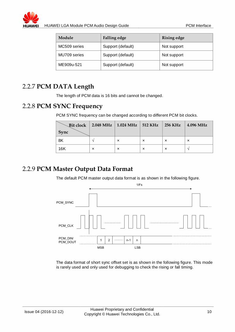
2.2.7 PCM DATA Length
The length of PCM data is 16 bits and cannot be changed.
2.2.8 PCM SYNC Frequency
PCM SYNC frequency can be changed according to different PCM bit clocks.
Bit clock
Sync
2.048 MHz 1.024 MHz 512 KHz 256 KHz 4.096 MHz
8K √ × × × ×
16K × × × × √
2.2.9 PCM Master Output Data Format
The default PCM master output data format is as shown in the following figure.
The data format of short sync offset set is as shown in the following figure. This mode is rarely used and only used for debugging to check the rising or fall timing.

HUAWEI LGA Module PCM Audio Design Guide PCM Interface
Issue 04 (2016-12-12) Huawei Proprietary and Confidential
Copyright © Huawei Technologies Co., Ltd. 11

HUAWEI LGA Module PCM Audio Design Guide Reference Design
Issue 04 (2016-12-12) Huawei Proprietary and Confidential
Copyright © Huawei Technologies Co., Ltd. 12
3 Reference Design
3.1 System Block It is recommended that Huawei LGA module should work in PCM master mode. It means PCM_CLK and PCM_SYNC are generated by Huawei LGA module.
The codec of TLV320AIC3204 and NAU8814 are recommended to be used.
If customers have the I2C or SPI communication bus, TLV320AIC3204 or NAU8814 is recommended to be used. The recommended connections of TLV320AIC3204 are as shown in the following figure.
LGA
Module
PCM_SYNC
PCM_DIN
PCM_DOUT
Codec:
TLV320AIC3204
PCM_SYNC
PCM_DIN
PCM_DOUT
5
6
7
I2C_DATA
I2C_CLK
MCU
I2C_DATA
I2C_CLK
PCM_CLK PCM_CLK
8
If customers have the communication bus and want to use NAU8814, the I2C of Huawei LGA module can be used. The module (MU709) can control NAU8814 by its I2C and does not need MCU anymore. In addition, Huawei LGA module provides AT^CPCM command to control NAU8814.

HUAWEI LGA Module PCM Audio Design Guide Reference Design
Issue 04 (2016-12-12) Huawei Proprietary and Confidential
Copyright © Huawei Technologies Co., Ltd. 13
The recommended connections of NAU8814 are as shown in the following figure. This solution needs the support of Huawei LGA module's software. If customers want to use this function, you should connect us for more information.
LGA
Module
PCM_SYNC
PCM_DIN
PCM_DOUT
PCM_CLK
Codec:
NAU8814
PCM_SYNC
PCM_DIN
PCM_DOUT
PCM_CLK
5
6
7
8
I2C_DATA
I2C_CLK
I2C_DATA
I2C_CLK60
61
PCM_MCLK
3.2 Reference Schematic and Software Configuration
3.2.1 TLV320AIC3204
HUAWEI LGA Module PCM Audio Design Guide Reference Design
Issue 04 (2016-12-12) Huawei Proprietary and Confidential
Copyright © Huawei Technologies Co., Ltd. 14
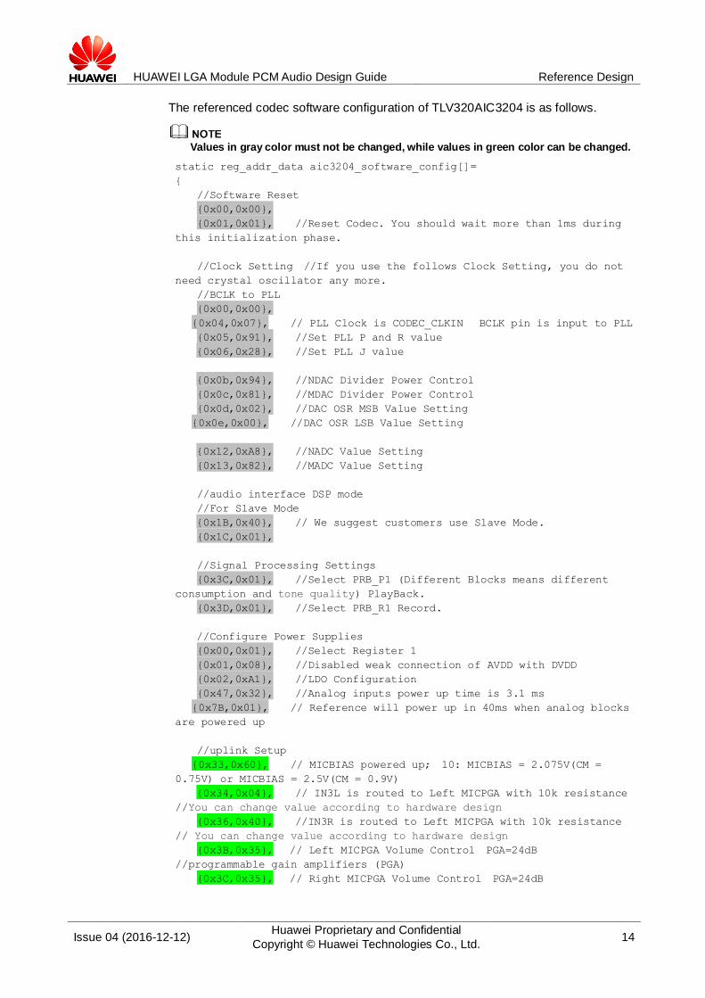
The referenced codec software configuration of TLV320AIC3204 is as follows.
Values in gray color must not be changed, while values in green color can be changed.
static reg_addr_data aic3204_software_config[]=
{
//Software Reset
{0x00,0x00},
{0x01,0x01}, //Reset Codec. You should wait more than 1ms during
this initialization phase.
//Clock Setting //If you use the follows Clock Setting, you do not
need crystal oscillator any more.
//BCLK to PLL
{0x00,0x00},
{0x04,0x07}, // PLL Clock is CODEC_CLKIN BCLK pin is input to PLL
{0x05,0x91}, //Set PLL P and R value
{0x06,0x28}, //Set PLL J value
{0x0b,0x94}, //NDAC Divider Power Control
{0x0c,0x81}, //MDAC Divider Power Control
{0x0d,0x02}, //DAC OSR MSB Value Setting
{0x0e,0x00}, //DAC OSR LSB Value Setting
{0x12,0xA8}, //NADC Value Setting
{0x13,0x82}, //MADC Value Setting
//audio interface DSP mode
//For Slave Mode
{0x1B,0x40}, // We suggest customers use Slave Mode.
{0x1C,0x01},
//Signal Processing Settings
{0x3C,0x01}, //Select PRB_P1 (Different Blocks means different
consumption and tone quality) PlayBack.
{0x3D,0x01}, //Select PRB_R1 Record.
//Configure Power Supplies
{0x00,0x01}, //Select Register 1
{0x01,0x08}, //Disabled weak connection of AVDD with DVDD
{0x02,0xA1}, //LDO Configuration
{0x47,0x32}, //Analog inputs power up time is 3.1 ms
{0x7B,0x01}, // Reference will power up in 40ms when analog blocks
are powered up
//uplink Setup
{0x33,0x60}, // MICBIAS powered up; 10: MICBIAS = 2.075V(CM =
0.75V) or MICBIAS = 2.5V(CM = 0.9V)
{0x34,0x04}, // IN3L is routed to Left MICPGA with 10k resistance
//You can change value according to hardware design
{0x36,0x40}, //IN3R is routed to Left MICPGA with 10k resistance
// You can change value according to hardware design
{0x3B,0x35}, // Left MICPGA Volume Control PGA=24dB
//programmable gain amplifiers (PGA)
{0x3C,0x35}, // Right MICPGA Volume Control PGA=24dB
HUAWEI LGA Module PCM Audio Design Guide Reference Design
Issue 04 (2016-12-12) Huawei Proprietary and Confidential
Copyright © Huawei Technologies Co., Ltd. 15
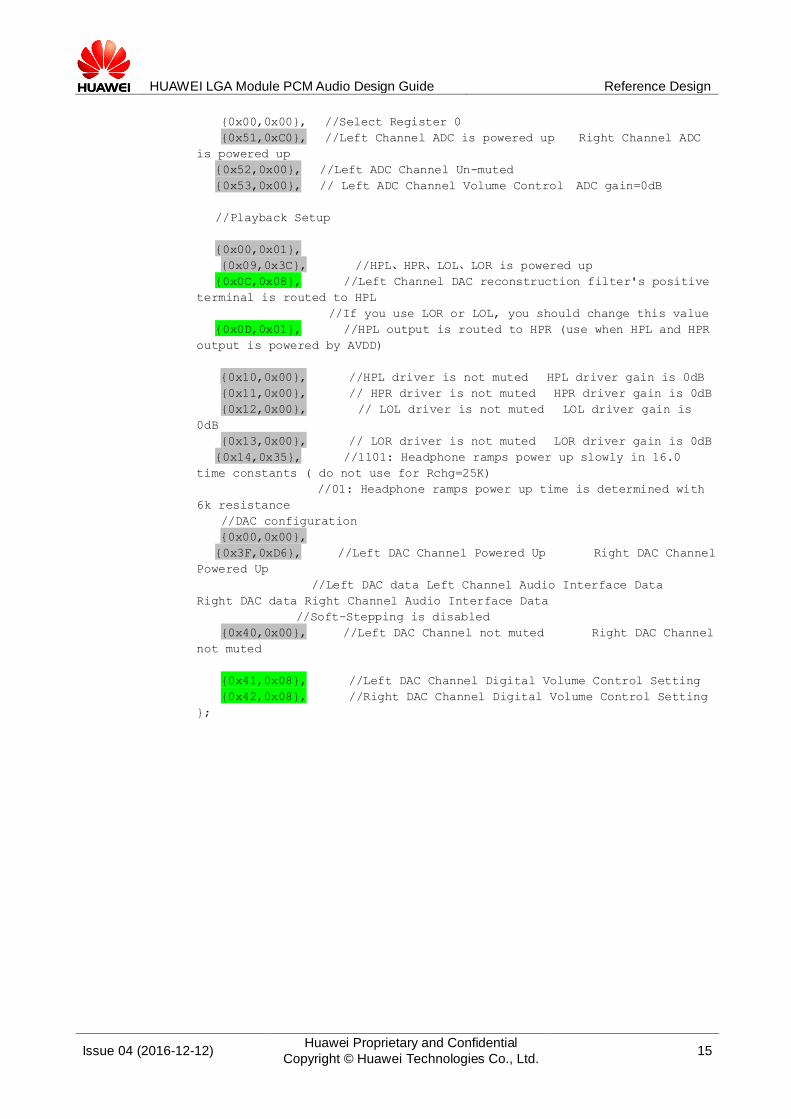
{0x00,0x00}, //Select Register 0
{0x51,0xC0}, //Left Channel ADC is powered up Right Channel ADC
is powered up
{0x52,0x00}, //Left ADC Channel Un-muted
{0x53,0x00}, // Left ADC Channel Volume Control ADC gain=0dB
//Playback Setup
{0x00,0x01},
{0x09,0x3C}, //HPL、HPR、LOL、LOR is powered up
{0x0C,0x08}, //Left Channel DAC reconstruction filter's positive
terminal is routed to HPL
//If you use LOR or LOL, you should change this value
{0x0D,0x01}, //HPL output is routed to HPR (use when HPL and HPR
output is powered by AVDD)
{0x10,0x00}, //HPL driver is not muted HPL driver gain is 0dB
{0x11,0x00}, // HPR driver is not muted HPR driver gain is 0dB
{0x12,0x00}, // LOL driver is not muted LOL driver gain is
0dB
{0x13,0x00}, // LOR driver is not muted LOR driver gain is 0dB
{0x14,0x35}, //1101: Headphone ramps power up slowly in 16.0
time constants ( do not use for Rchg=25K)
//01: Headphone ramps power up time is determined with
6k resistance
//DAC configuration
{0x00,0x00},
{0x3F,0xD6}, //Left DAC Channel Powered Up Right DAC Channel
Powered Up
//Left DAC data Left Channel Audio Interface Data
Right DAC data Right Channel Audio Interface Data
//Soft-Stepping is disabled
{0x40,0x00}, //Left DAC Channel not muted Right DAC Channel
not muted
{0x41,0x08}, //Left DAC Channel Digital Volume Control Setting
{0x42,0x08}, //Right DAC Channel Digital Volume Control Setting
};

HUAWEI LGA Module PCM Audio Design Guide Reference Design
Issue 04 (2016-12-12) Huawei Proprietary and Confidential
Copyright © Huawei Technologies Co., Ltd. 16
AT^CPCM is the AT command for the configuration of PCM. For the details, please refer to the module's AT command interface specification. If using the codec configuration above, you cannot change parameter values of AT^CPCM, but you can run AT^CPCM=0,0,0,0,0 to set them to default values.
3.2.2 NAU8814
The referenced design of NAU8814 is as shown in the following figure. For details,
please refer to NAU8814 official website.
SPI_Select
IN1_R
IN2_R
IN3_R
IN3_L
IN2_L
IN1_L
ZS
S/L
CS
Left
ADC
DRC
tplLeft
DAC
AGC
ADC
Signal
Proc.
DAC
Signal
Proc.
Right
ADC
DRC
tprRightDAC
AGC
ADC
Signal
Proc.
DAC
Signal
Proc.
Vol. Ctrl
Vol . Ctrl
Data
Interface
Gain Adj.
Gain Adj.
0…
+47.5 dB
0…+47.5 dB
0.5 dB
steps
-6...+29dB
-6...+29dB
-6...+29dB
-6...+29dB
SPI / I2C Secondary
I2
Primary
I2
Digital
Mic.
Interrupt
Ctrl
ALDO
DLDO
PLL
Mic
Bias
Ref
MicBias
Ref
tc
ele
SO
DL
Supplies
niO
DL
HPVdd
dd
VD
dd
VA
dd
VOI
ss
VA
ss
VD
ss
VOI
IS
OM/
AD
S
OSI
M
KL
CS
KL
CM
OIP
G
TU
OD
NID
KL
CB
KL
CW
miniDSP miniDSP
HPL
LOL
HPR
LOR
Reset
-30...0 dB
-30...0 dB
-72...0dB
-72...0dB

HUAWEI LGA Module PCM Audio Design Guide Reference Design
Issue 04 (2016-12-12) Huawei Proprietary and Confidential
Copyright © Huawei Technologies Co., Ltd. 17
LGA
Module
PCM_SYNC
PCM_DIN
PCM_DOUT
PCM_CLK
Codec:
NAU8814
FS
DACIN
ADCOUT
BCLK
SDIN
SCLK
I2C_DATA
I2C_CLK
MCLK
9
7
8
10
11
5
6
7
8
61
60
14
13
15
12
MODE
CSb/GPIO
VDDA
VDDC
VDDB
VSSA
VREF
VDDSPK
VSSD
25
4
36
22
20
18VSSSPK
3.3V32VCC_EXT1
4.7uF
1.8V
3.3V
4.7uF
4.7uF
4.7uF
1 24
23
21
19
17
16
MIC
BIA
S
MIC
-
MIC
+
AU
X
SP
KO
UT
-
SP
KO
UT
+ MO
UT
SPKMIC
1.2k
1uF 1uF
1.2k
33pF
33pF
33pF 33pF
1uF
AUX
1uF
MOUT
4.7uF
1.2k 1.2k
The referenced codec software configuration of NAU8814 is as follows.
static REGISTER_SETTING_T sNA8814_CODEC_SETTING[]=
{
{0x01,0x001d},
{0x02,0x0015},
{0x03,0x0065},
{0x04,0x0118},
{0x06,0x0000},
{0x07,0x000A},
{0x0E,0x01B8},
{0x2d,0x00b0},
{0x36,0x003f}
};

HUAWEI LGA Module PCM Audio Design Guide Reference Design
Issue 04 (2016-12-12) Huawei Proprietary and Confidential
Copyright © Huawei Technologies Co., Ltd. 18
AT^CPCM is the AT command for the configuration of PCM. For the details, please refer to the module's AT command interface specification.
If using the codec configuration above, you need to keep parameter values of AT^CPCM as default values.
If you want to use the module’s I2C to control NAU8814, please run
AT^CODECPOW=1 firstly and then dial others.


