
PCIE-1813 User Manual Ed.2 FINAL - Advantech
62
User Manual PCIE-1813 38.4 kS/s, 26-Bit, 4-Ch, Simultaneous Sampling, Universal Bridge Input, Multifunction PCI Express Card
Transcript of PCIE-1813 User Manual Ed.2 FINAL - Advantech

User Manual
PCIE-1813
38.4 kS/s, 26-Bit, 4-Ch, Simultaneous Sampling, Universal Bridge Input,Multifunction PCI Express Card

PCIE-1813 User Manual ii
CopyrightThis documentation and the software included with this product are copyrighted 2020by Advantech Co., Ltd. All rights are reserved. Advantech Co., Ltd. reserves the rightto improve the products described in this manual at any time without notice. No partof this manual may be reproduced, copied, translated, or transmitted in any form orby any means without the prior written permission of Advantech Co., Ltd. The infor-mation provided in this manual is intended to be accurate and reliable. However,Advantech Co., Ltd. assumes no responsibility for its use, nor for any infringementsof the rights of third parties that may result from its use.
AcknowledgmentsIntel and Pentium are trademarks of Intel Corporation.Microsoft Windows and MS-DOS are registered trademarks of Microsoft Corp.All other product names or trademarks are properties of their respective owners.
Product Warranty (2 years)Advantech warrants the original purchaser that each of its products will be free fromdefects in materials and workmanship for two years from the date of purchase. This warranty does not apply to any products that have been repaired or altered bypersons other than repair personnel authorized by Advantech, or products that havebeen subject to misuse, abuse, accident, or improper installation. Advantechassumes no liability under the terms of this warranty as a consequence of suchevents.Because of Advantech’s high quality-control standards and rigorous testing, mostcustomers never need to use our repair service. If an Advantech product is defective,it will be repaired or replaced at no charge during the warranty period. For out-of-war-ranty repairs, users are billed according to the cost of replacement materials, servicetime, and freight. Consult your dealer for more details.If you suspect that your product is defective, follow the steps outlined below:1. Collect all the information about the problem encountered. (For example, CPU
speed, Advantech products used, other hardware and software used, etc.) Note anything abnormal and list any on-screen messages displayed when the prob-lem occurs.
2. Call your dealer and describe the problem. Have your manual, product, and any helpful information readily available.
3. If your product is diagnosed as defective, obtain an return merchandise authori-zation (RMA) number from your dealer. This allows us to process your return more quickly.
4. Carefully pack the defective product, a completed Repair and Replacement Order Card and a proof of purchase date (such as a photocopy of your sales receipt) into a shippable container. Products returned without a proof of pur-chase date are not eligible for warranty service.
5. Write the RMA number clearly on the outside of the packaging and ship the package prepaid to your dealer.
Part No. 2001181311 Edition 2Printed in Taiwan May 2020

iii PCIE-1813 User Manual
CEThis product has passed the CE test for environmental specifications when shieldedcables are used for external wiring. We recommend the use of shielded cables. Suchcables are available from Advantech. Please contact your local supplier for orderinginformation.
Technical Support and Assistance1. Visit the Advantech website at http://support.advantech.com.tw/ to obtain the
latest product information.2. Contact your distributor, sales representative, or Advantech's customer service
center for technical support if you need additional assistance. Have the follow-ing information ready before you call:– Product name and serial number– Description of your peripheral attachments– Description of your software (operating system, version, application software,
etc.)– A comprehensive description of the problem– The exact wording of any error messages
Packing ListBefore setting up the system, check that the items listed below are included and ingood condition. If any of the items are missing or damaged, contact your dealerimmediately. 1 x PCIE-1813 DA&C card 1 x user manual 1 x DVD-ROM with DAQ Navi drivers
Safety Precautions - Static ElectricityFollow the simple precautions below to protect yourself from harm and the productsfrom damage.1. To avoid electrical shock, always disconnect the power from the PC chassis
before manual handling. Do not touch any components on the CPU card or other cards when the PC is powered on.
2. Disconnect the power before implementing any configuration changes. The sud-den rush of power after connecting a jumper or installing a card may damage sensitive electronic components.

PCIE-1813 User Manual iv

v PCIE-1813 User Manual
ContentsChapter 1 Introduction..........................................1
1.1 Features .................................................................................................... 21.2 Applications............................................................................................... 31.3 Installation Guide ...................................................................................... 3
Figure 1.1 Installation flowchart ................................................... 41.4 Software Overview.................................................................................... 51.5 DAQNavi Device Driver Programming Roadmap ..................................... 51.6 Accessories............................................................................................... 6
Chapter 2 Installation............................................72.1 Unpacking ................................................................................................. 82.2 Driver Installation ...................................................................................... 9
Figure 2.1 Advantech automation software setup screen............ 9Figure 2.2 The various options for driver setup ......................... 10
2.3 Hardware Installation ............................................................................. 102.4 Device Setup and Configuration ............................................................. 11
Figure 2.3 PCIE-1813 device settings ....................................... 11Figure 2.4 Device settings page ................................................ 12Figure 2.5 PCIE-1813 device testing ......................................... 12
Chapter 3 Signal Connections ...........................133.1 Overview ................................................................................................. 143.2 Switch and Jumper Settings.................................................................... 14
Figure 3.1 Connector and switch locations................................ 143.2.1 Board ID (SW1)........................................................................... 15
Table 3.1: Board ID Setting (SW1) ............................................ 153.2.2 Power On Configuration (JP1) .................................................... 15
Table 3.2: Power on Configuration after Hot Reset (JP1) ......... 153.3 Signal Connections ................................................................................. 16
Figure 3.2 100-pin I/O connector pin assignments .................... 163.3.1 I/O Connector Signal Description................................................ 17
3.4 Analog Input ............................................................................................ 193.4.1 Analog Input Overview................................................................ 193.4.2 Connecting Signals ..................................................................... 20
Figure 3.3 Basic Wheatstone bridge circuit diagram ................. 203.4.3 Strain Gauge Sensor Configurations .......................................... 21
Figure 3.4 Quarter-bridge type I measuring axial and bending strain......................................................................... 21
Figure 3.5 Quarter-bridge type I circuit diagram........................ 21Figure 3.6 Quarter-bridge type II measuring axial and bending
strain......................................................................... 22Figure 3.7 Quarter-bridge type I circuit diagram........................ 22Figure 3.8 Half-bridge type I measuring axial and bending strain .
23Figure 3.9 Half-bridge type I circuit diagram.............................. 23Figure 3.10Half-bridge type II rejecting axial and measuring bend-
ing strain ................................................................... 24Figure 3.11Half-bridge type II circuit diagram............................. 24Figure 3.12Full-bridge type I rejecting axial and measuring bending
strain......................................................................... 25Figure 3.13Full-bridge type I circuit diagram .............................. 25

PCIE-1813 User Manual vi
Figure 3.14Full-bridge type II rejecting axial and measuring bend-ing strain................................................................... 26
Figure 3.15Full-bridge type II circuit diagram ............................. 26Figure 3.16Full-bridge type III rejecting axial and measuring bend-
ing strain................................................................... 27Figure 3.17Full-bridge type III circuit diagram ............................ 27Figure 3.18Full-bridge type III circuit diagram ............................ 28Figure 3.19External clock source connection............................. 29Figure 3.20External digital trigger source connection ................ 29Figure 3.21External analog trigger source connection ............... 30Figure 3.22Analog output connections ....................................... 31Figure 3.23External clock source connection............................. 32Figure 3.24External digital trigger source connection ................ 32
3.4.4 Digital Signal Connections.......................................................... 33Figure 3.25Wet and dry contacts................................................ 33Figure 3.26Digital input wet signal connection ........................... 33Figure 3.27Digital input dry signal connection............................ 33Figure 3.28Digital output channel connections........................... 34
3.5 Field Wiring Considerations .................................................................... 34
Appendix A Specifications.................................... 35A.1 Function Block ........................................................................................ 36A.2 Analog Input............................................................................................ 37A.3 Analog Output ......................................................................................... 38A.4 Digital Input/Output ................................................................................. 38A.5 Counter/Timer ......................................................................................... 39A.6 General ................................................................................................... 39
Appendix B Operation Theory .............................. 41B.1 Analog Input Operation ........................................................................... 42
B.1.1 AI Hardware Structure ................................................................ 42B.1.2 Analog Input Ranges and Gains................................................. 42
Table B.1: Gains and Analog Input Range ................................ 42B.1.3 AI Trigger Modes ........................................................................ 43B.1.4 AI CONV Clock Source............................................................... 45B.1.5 AI Trigger Source........................................................................ 46
Table B.2: Analog Input Data Format ........................................ 46Table B.3: Full-Scale Values for Input Voltage Ranges............. 46
B.2 PCIE-1813 Analog Output Operation...................................................... 46B.2.1 Analog Output Ranges ............................................................... 47B.2.2 Analog Output Operation Modes ................................................ 47B.2.3 AO Clock Sources ...................................................................... 48B.2.4 AO Trigger Sources.................................................................... 48
Table B.4: Analog Output Data Format ..................................... 48Table B.5: Full-Scale Values for Output Voltage Ranges.......... 48
B.3 Digital Input/Output Operation ................................................................ 49B.4 Counter Input and PWM Input/Output..................................................... 49

Chapter 11 IntroductionThis chapter introduces PCIE-1813 and its typical applications.
FeaturesApplications Installation GuideSoftware OverviewRoadmapAccessories

PCIE-1813 User Manual 2
The PCIE-1813 is a 26-bit high-resolution multi-function data acquisition PCI Expresscard which integrates 4-ch analog inputs, 2-ch analog outputs, 32-ch digital I/Os, and4 encoder (or general purpose) counters. 26-bit AI conversion (voltage and universal bridge input) 16-bit AO conversion Digital input Digital output Encoder counter/ TimerPCIE-1813 is an advanced high-performance multifunction card based on the PCIex1 Bus. With a large FIFO of 1K Sample, the maximum sampling rate of PCIE-1813is up to 38.4 KS/s with 4 A/D converters simultaneously sampling on each channel.The PCIE-1813 has two 16-bit D/A output channels, 32 digital input/output channels,and four 32-bit Time/counter channels so that it can provide specific functions for dif-ferent application requirements.
1.1 Features Four differential simultaneous sampling voltage and universal inputs 26-bit AI converter, up to 38.4 kS/s sampling rate for each channel Start-, Delay to Start-, Delay to Stop-, Stop-event trigger capable Programmable gain for each input channel 1K and 8K onboard buffer for analog input and analog output respectively Two independent 16-bit analog output channels with continuous waveform out-
put function of maximum 3 MHz throughput rate Auto-calibration for analog input and output channels System calibration for bridge input signals 32 digital Input or output channels, TTL compatible Four 32-bit independent encoder (or general purpose) counters BoardID switch
PCIE-1813 offers the following main features: PCIe-Bus Plug & Play The PCIE-1813 card uses a PCIe controller to interface the card to the PCI Expressbus. The controller fully implements the PCI Express Base Specification v1.1. All con-figurations related to the bus, such as base address and interrupt assignment, areautomatically controlled by software. No jumper or switch is required for user configu-ration.
Four A/D Converters for Simultaneous SamplingPCIE-1813 card is capable of simultaneous sampling with dedicated A/D convertercircuit for each analog input channel.
Onboard Buffer Memory There are 1K and 8K sample buffers for AI and AO respectively on PCIE-1813. Thisis an important feature for faster data transfer and more predictable performanceunder Windows systems.

3 PCIE-1813 User Manual
Chapter 1
Introduction
Onboard Programmable Encoder (or General Purpose) CountersThe PCIE-1813 features four 32-bit encoder (or general purpose) counters to provideencoder input, encoder compare output, one shot output, PWM output, periodic inter-rupt output, time-delay output, and the measurement of frequency and pulse width. BoardID Switch The PCIE-1813 has a built-in DIP switch that helps define each card’s ID when multi-ple PCIE-1813 cards have been installed on the same PC chassis. The BoardID set-ting function is very useful when building a system with multiple PCIE-1813 cards.With the correct BoardID settings, you can easily identify and access each cardduring hardware configuration and software programming.
1.2 Applications Load cell and strain gauge measurements Waveform acquisition and analysis Process control and monitoring
1.3 Installation Guide Before you install your PCIE-1813 card, please make sure you have the followingnecessary components: PCIE-1813 DA&C card PCIE-1813 User Manual Driver software Advantech DAQNavi software (included in the companion DVD-
ROM) Personal computer or workstation with a PCI Express interface (running
Windows 10, 8 and 7) Shielded Cable PCL-101100R (optional) Wiring Board ADAM-39100 (optional)
Other optional components are also available for enhanced operation: DAQ Navi, LabView or other 3rd-party software
After you get the necessary components and maybe some of the accessories forenhanced operation of your multifunction card, you can then begin the installationprocedure. Figure 1.1 on the next page provides the broad installation steps:
Note! For detailed specifications and operations of PCIE-1813, please refer to Appendices A and B.

PCIE-1813 User Manual 4
Figure 1.1 Installation flowchart

5 PCIE-1813 User Manual
Chapter 1
Introduction
1.4 Software Overview Advantech offers a rich set of DLL drivers, third-party driver support, and applicationsoftware to help fully exploit the functions of your PCIE-1813 card: Device Drivers (on the companion DVD-ROM) LabVIEW driver Advantech DAQNavi Data logger
Programming Choices for DA&C Cards You may use Advantech application software such as Advantech Device Drivers. Onthe other hand, advanced users can use register-level programming, although this isnot recommended due to its laborious and time-consuming nature.
DAQNavi SoftwareAdvantech DAQNavi software includes device drivers and an SDK, which features acomplete I/O function library to help boost your application performance. This soft-ware is included in the companion DVD-ROM at no extra charge and comes with allAdvantech DA&C cards. The Advantech DAQNavi software for Windows XP/7/8 (desktop mode) works seamlessly with development tools such as Visual Studio.NET, Visual C++, Visual Basic and Borland Delphi.
1.5 DAQNavi Device Driver Programming Roadmap This section will provide you with a roadmap to demonstrate how to build an applica-tion from scratch using Advantech DAQNavi Device Driver with your favorite devel-opment tools such as Visual Studio .NET, Visual C++, Visual Basic, Delphi, and C++Builder. The step-by-step instructions on how to build your own applications usingeach development tool is given in the Device Drivers Manual. A rich set of examplesource code is also provided for your reference.
Programming Tools Programmers can develop application programs with their favorite developmenttools: Visual Studio .NET Visual C++ and Visual Basic Delphi C++ Builder For instructions on how to begin programming work in each development tool,Advantech offers a Tutorial Chapter in the DAQNavi SDK Manual for your reference.Please refer to the corresponding sections in this chapter on the DAQNavi SDK Man-ual to begin your programming effort. You can also look at the example source codeprovided for each programming tool; examples can help jump-start a project. The DAQNavi SDK Manual can be found on the companion DVD-ROM. Alternatively,if you have already installed the Device Drivers on your system, The DAQNavi SDKManual can be readily accessed through the Start button: Start/Programs/Advantech Automation/DAQNavi/DAQNavi Manuals/DAQNaviSDK ManualThe example source code can be found under the corresponding installation foldersuch as the default installation path: \Advantech\DAQNavi\Examples

PCIE-1813 User Manual 6
For information about using other function groups or other development tools, pleaserefer to the Using DAQNavi SDK chapter in the DAQNavi SDK Manual, or the videotutorials in the Advantech Navigator.
Programming with DAQNavi Device Drivers Function Library Advantech DAQNavi Device Drivers offer a rich function library that can be utilized invarious application programs. This function library consists of numerous APIs thatsupport many development tools, such as Visual Studio .NET, Visual C++, VisualBasic, Delphi and C++ Builder. According to their functions or services, APIs can be categorized into several functiongroups: Analog Input Function Group Analog Output Function Group Digital Input/Output Function Group Counter Function Group Port Function Group (direct I/O) Event Function Group For the usage and parameters of each function, please refer to the Using DAQNaviSDK chapter in the DAQNavi SDK Manual.
Troubleshooting DAQNavi Device Drivers Error Driver functions will return a status code when they are called to perform a certaintask for the application. When a function returns a code that is not zero, it means thefunction has failed to perform its designated function. To troubleshoot the DeviceDrivers error, you can pass the error, you can check the error code and error descrip-tion within the Error Control of each function in the DAQNavi SDK Manual.
1.6 Accessories Advantech offers a complete set of accessory products to support the PCIE-1813card. These accessories include: Wiring Cables PCL-101100R-1E 100-pin SCSI (ribbon type) shielded cable, 1m PCL-101100R-2E 100-pin SCSI (ribbon type) shielded cable, 2m
Wiring Boards ADAM-39100-AE 100-pin DIN-rail SCSI wiring board PCLD-8813-AE 100-pin DIN-rail SCSI wiring board with isolation

Chapter 22 InstallationThis chapter provides a packing item checklist, proper instructions for unpacking, and step-by-step procedures for both driver and card installation.
UnpackingDriver InstallationHardware InstallationDevice Setup and Configuration
PCIE-1813 User Manual 8
2.1 UnpackingAfter receiving your PCIE-1813 package, inspect the contents. The package shouldinclude the following items: PCIE-1813 card Companion DVD-ROM (Device Drivers included) Startup Manual
The PCIE-1813 card has certain electronic components vulnerable to electrostaticdischarge (ESD). ESD can easily damage the integrated circuits and certain compo-nents if preventive measures are ignored.
Before removing the card from the anti-static plastic bag, you should take followingprecautions to ward off possible ESD damage: Touch the metal part of your computer chassis with your hand to discharge the
static electricity accumulated on your body. Alternatively, one can also use a grounding strap.
Touch the anti-static bag to a metal part of your computer chassis before open-ing the bag.
Take hold of the card only by the metal bracket when removing it from the bag. After taking out the card, you should first: Inspect the card for any possible signs of external damage (loose or damaged
components, etc.). If the card is visibly damaged, please notify our service department or our local sales representative immediately. Do not install a dam-aged card into your system.
Also pay extra attention to the following to ensure a proper installation: Avoid physical contact with materials that could hold static electricity such as
plastic, vinyl and styrofoam. Whenever you handle the card, grasp it only by its edges. DO NOT TOUCH the
exposed metal pins of the connector or the electronic components.
Note! Keep the anti-static bag for future use. You might need the original bag to store the card if you have to remove the card from a PC or transport it elsewhere.

9 PCIE-1813 User Manual
Chapter 2
Installation
2.2 Driver InstallationWe recommend you install the driver before you install the PCIE-1813 card into yoursystem, since this will guarantee a smooth installation process. The Advantech DAQNavi Device Drivers Setup program for the PCIE-1813 card isincluded in the companion DVD-ROM that is shipped with your DA&C card package.Please follow the steps below to install the driver software: 1. Insert the companion DVD-ROM into the DVD-ROM drive.2. The Setup program should launch automatically if you have the autoplay func-
tion enabled on your system. When the Setup Program is launched, you will see the following Setup Screen.
Figure 2.1 Advantech automation software setup screen
3. Select the Installation option.4. Select the Legacy SDK and Drivers option to install. 5. Select the Individual Drivers option. 6. Select the PCIe series and the specific device then follow the installation
instructions step by step to complete your device driver installation and setup.7. Press the Back button and select the Windows SDK and Drivers and install the
Advantech Navigator.
Note! If the autoplay function is not enabled on your computer, use Windows Explorer or Windows Run command to execute autorun.exe on the companion DVD-ROM.

PCIE-1813 User Manual 10
Figure 2.2 The various options for driver setupFor further information on driver-related issues, an online version of the DAQNaviSDK Manual is available by accessing the following path: Start/Programs/Advantech Automation/DAQNavi/DAQNavi Manuals/DAQNavi SDKManual
2.3 Hardware Installation
After installing the device drivers, install the PCIE-1813 card in the computer. How-ever, it is suggested that you refer to the computer’s user manual or related docu-mentation if you have any doubts. Please follow the steps below to install the card inyour system. 1. Power off your computer and unplug the power cord and cables. Do this before
installing or removing any components on the computer. 2. Remove the cover of your computer. 3. Remove the slot cover on the back panel of your computer. 4. Touch the metal part on the surface of your computer to neutralize any static
electricity that might be on your body. 5. Insert the PCIE-1813 card into the PCI Express interface. Hold the card only by
its edges and carefully align it with the slot. Insert the card firmly into place. Use of excessive force must be avoided; otherwise, the card might be damaged.
6. Connect appropriate accessories (100-pin SCSI shielded cable, wiring termi-nals, etc., if necessary) to the card.
7. Replace the cover of your computer chassis. Re-connect the cables you removed in step 1.
8. Plug in the power cord and turn on the computer.
Note! Make sure you have installed the driver first before you install the card (refer to 2.2 Driver Installation)

11 PCIE-1813 User Manual
Chapter 2
Installation
After your card is properly installed on your system, you can now configure yourdevice using the Advantech Navigator Program that has itself already been installedon your system during driver setup. A complete device installation procedure shouldinclude device setup, configuration and testing. The following sections will guide youthrough the Setup, Configuration and Testing of your device.
2.4 Device Setup and Configuration The Advantech Navigator program is a utility that allows you to set up, configure andtest your device, and later stores your settings on the system registry. These settingswill be used when you call the APIs of Advantech Device Drivers. Take the followingPCIE-1813 details as an example.
Setting Up the Device1. To install the I/O device for your card, first run the Advantech Navigator program
(by accessing Start/Programs/Advantech Automation/Navigator for DN4). 2. You can then view the device(s) already installed on your system (if any) in the
Installed Devices list box. If the software and hardware installation are com-pleted, you will see PCIE-1813 card in the Installed Devices list.
Figure 2.3 PCIE-1813 device settings

PCIE-1813 User Manual 12
Configuring the Device 3. Go to Device Setting to configure your device. Here you can configure not only
the Analog Input/Output of PCIE-1813 but also Digital Input/Output.
Figure 2.4 Device settings page
4. After your card is properly installed and configured, you can go to the Device Test page to test the hardware using the testing utility supplied.
Figure 2.5 PCIE-1813 device testing
For more detailed information, please refer to the DAQNavi SDK manual or the userinterface manual in the Advantech Navigator.

Chapter 33 Signal ConnectionsThis chapter provides useful information about how to connect input and output signals to the PCIE-1813 card via the I/O con-nector.
Overview Board ID Settings Signal Connections Analog Input Field Wiring Considerations

PCIE-1813 User Manual 14
3.1 Overview Maintaining signal connections is one of the most important factors in ensuring thatyour application system is sending and receiving data correctly. A good signal con-nection can avoid unnecessary and costly damage to your PC and other hardwaredevices. This chapter provides useful information about how to connect input andoutput signals to the PCIE-1813 card via the I/O connector.
3.2 Switch and Jumper Settings Please refer to Figure 3.1 for jumper and switch locations on PCIE-1813.
Figure 3.1 Connector and switch locations

15 PCIE-1813 User Manual
Chapter 3
Signal Connections
3.2.1 Board ID (SW1)The PCIE-1813 has a built-in DIP switch (SW1), which is used to define each card’sboard ID. When there are multiple cards on the same chassis, this board ID switch isused to set each card’s device number.After setting each PCIE-1813, you can identify each card in system with differentdevice numbers. The default value of board ID is 0 and if you need to adjust it toother value, set the SW1 by referring to Table 3.1.
Default Setting is 0
3.2.2 Power On Configuration (JP1)Default configuration after power on, and hardware reset is to set all the digital outputand analog output channels to open status (output voltage equals zero) so that exter-nal devices will not be damaged when the system starts or resets. When the systemis hot reset, then the status of isolated digital output channels are selected by jumperJP1. Table 3.2 shows the possible configurations of jumper JP1.
Table 3.1: Board ID Setting (SW1) SW1 Position 1 Position 2 Position 3 Position 4BoardID Bit0 Bit1 Bit2 Bit30 ON ON ON ON1 ON ON ON OFF 2 ON ON OFF ON3 ON ON OFF OFF 4 ON OFF ON OFF 5 ON OFF ON OFF 6 ON OFF OFF ON7 ON OFF OFF OFF 8 OFF ON ON ON9 OFF ON ON OFF 10 OFF ON OFF ON11 OFF ON OFF OFF 12 OFF OFF ON ON13 OFF OFF ON OFF 14 OFF OFF OFF ON15 OFF OFF OFF OFF
Table 3.2: Power on Configuration after Hot Reset (JP1)JP1 Power on configuration after hot reset 1
Keep same status as before reset
1Default configuration (DO status low)

PCIE-1813 User Manual 16
3.3 Signal Connections Pin Assignments The I/O connector on the PCIE-1813 is a 100-pin connector that enables you to con-nect to accessories with the PCL-101100R shielded cable.Figure 3.2 shows the pin assignments for the 100-pin I/O connector on PCIE-1813,and its I/O connector signal description.
Figure 3.2 100-pin I/O connector pin assignments

17 PCIE-1813 User Manual
Chapter 3
Signal Connections
3.3.1 I/O Connector Signal Description
Pin Name Type Pin# Description
Analog InputAI0+ I 100 Positive terminal of analog input channel 0AI0- I 50 Negative terminal of analog input channel 0RS0+ I 99 Positive remote sensing terminal of AI 0RS0- I 49 Negative remote sensing terminal of AI 0EX0+ O 98 Positive excitation voltage terminal of AI 0EX0- O 48 Negative excitation voltage terminal of AI 0QTR/SC0 - 97 Quarter bridge completion/shunt calibration terminal of AI 0QTR/SC1 - 47 Quarter bridge completion/shunt calibration terminal of AI 1AI1+ I 96 Positive terminal of analog input channel 1AI1- I 46 Negative terminal of analog input channel 1RS1+ I 95 Positive remote sensing terminal of AI 1RS1- I 45 Negative remote sensing terminal of AI 1EX1+ O 94 Positive excitation voltage terminal of AI 1EX1- O 44 Negative excitation voltage terminal of AI 1AI2+ I 93 Positive terminal of analog input channel 2AI2- I 43 Negative terminal of analog input channel 2RS2+ I 92 Positive remote sensing terminal of AI 2RS2- I 42 Negative remote sensing terminal of AI 2EX2+ O 91 Positive excitation voltage terminal of AI 2EX2- O 41 Negative excitation voltage terminal of AI 2QTR/SC2 - 90 Quarter bridge completion/shunt calibration terminal of AI 2QTR/SC3 - 40 Quarter bridge completion/shunt calibration terminal of AI 3AI3+ I 89 Positive terminal of analog input channel 3AI3- I 39 Negative terminal of analog input channel 3RS3+ I 88 Positive remote sensing terminal of AI 3RS3- I 38 Negative remote sensing terminal of AI 3EX3+ O 87 Positive excitation voltage terminal of AI 3EX3- O 37 Negative excitation voltage terminal of AI 3Analog OutputAO0_REF I 86 External reference voltage input for analog output channel 0AO0_OUT O 85 Voltage output of analog output channel 0AO1_REF I 36 External reference voltage input for analog output channel 1AO1_OUT O 35 Voltage output of analog output channel 1Timing Signals
ATRG0 I 83 Analog threshold trigger input channel 0
ATRG1 I 33 Analog threshold trigger input channel 1DTRG0 I 82 Digital trigger input channel 0DTRG1 I 32 Digital trigger input channel 1AI_CONV I 31 External analog input conversion clockAO_CONV I 30 External analog output conversion clockDigital Input/OutputDIO0 I/O 78 Digital input/output channel 0

PCIE-1813 User Manual 18
DIO1 I/O 28 Digital input/output channel 1DIO2 I/O 77 Digital input/output channel 2DIO3 I/O 27 Digital input/output channel 3DIO4 I/O 76 Digital input/output channel 4DIO5 I/O 26 Digital input/output channel 5DIO6 I/O 75 Digital input/output channel 6DIO7 I/O 25 Digital input/output channel 7DIO8 I/O 74 Digital input/output channel 8DIO9 I/O 24 Digital input/output channel 9DIO10 I/O 73 Digital input/output channel 10DIO11 I/O 23 Digital input/output channel 11DIO12 I/O 72 Digital input/output channel 12DIO13 I/O 22 Digital input/output channel 13DIO14 I/O 71 Digital input/output channel 14DIO15 I/O 21 Digital input/output channel 15DIO16 I/O 70 Digital input/output channel 16DIO17 I/O 20 Digital input/output channel 17DIO18 I/O 69 Digital input/output channel 18DIO19 I/O 19 Digital input/output channel 19DIO20 I/O 68 Digital input/output channel 20DIO21 I/O 18 Digital input/output channel 21DIO22 I/O 67 Digital input/output channel 22DIO23 I/O 17 Digital input/output channel 23DIO24 I/O 66 Digital input/output channel 24DIO25 I/O 16 Digital input/output channel 25DIO26 I/O 65 Digital input/output channel 26DIO27 I/O 15 Digital input/output channel 27DIO28 I/O 64 Digital input/output channel 28DIO29 I/O 14 Digital input/output channel 29DIO30 I/O 63 Digital input/output channel 30DIO31 I/O 13 Digital input/output channel 31Counter
CNT0_CLK/A I 61 Clock input (general purpose counter) or signal A input (encoder counter) of counter channel 0
CNT0_ B I 60 Signal B input (encoder counter) of counter channel 0
CNT0_GATE/Z I 59 Gate input (general purpose counter) or signal Z input (encoder counter) of counter channel 0
CNT0_SCLK/L I 58 Sample clock input (general purpose counter) orlatch input (encoder counter) of counter channel 0
CNT0_OUT O 57 Output of counter channel 0
CNT1_CLK/A I 11 Clock input (general purpose counter) or signal A input (encoder counter) of counter channel 1
CNT1_B I 10 Signal B input (encoder counter) of counter channel 1
CNT1_GATE/Z I 9 Gate input (general purpose counter) or signal Z input (encoder counter) of counter channel 1
CNT1_SCLK/L I 8 Sample clock input (general purpose counter) orlatch input (encoder counter) of counter channel 1
CNT1_OUT O 7 Output of counter channel 1

19 PCIE-1813 User Manual
Chapter 3
Signal Connections
3.4 Analog Input 3.4.1 Analog Input Overview
The analog input function of the PCIE-1813 has 26-bit resolution and supports sam-ple rates up to 38.4 kS/s.You can configure all settings on every single channel basis in software. The chan-nels support the following features: Voltage and ratio metric (mV/V) measurements. Connecting sensors of all bridge configurations, including quarter-, half-, and
full-bridge. DC voltage excitation between 0.5 V and 10V. Programmatic system calibration. Analog and digital filtering to reject out-of-band signals. Remote sense of bridge excitation.
CNT2_CLK/A I 56 Clock input (general purpose counter) or signal A input (encoder counter) of counter channel 2
CNT2_ B I 55 Signal B input (encoder counter) of counter channel 2
CNT2_GATE/Z I 54 Gate input (general purpose counter) or signal Z input (encoder counter) of counter channel 2
CNT2_SCLK/L I 53 Sample clock input (general purpose counter) orlatch input (encoder counter) of counter channel 2
CNT2_OUT O 52 Output of counter channel 2
CNT3_CLK/A I 6 Clock input (general purpose counter) or signal A input (encoder counter) of counter channel 3
CNT3_B I 5 Signal B input (encoder counter) of counter channel 3
CNT3_GATE/Z I 4 Gate input (general purpose counter) or signal Z input (encoder counter) of counter channel 3
CNT3_SCLK/L I 3 Sample clock input (general purpose counter) orlatch input (encoder counter) of counter channel 3
CNT3_OUT O 2 Output of counter channel 3Power and Ground
AGND -
34, 38, 40, 42, 45, 47, 49, 84
Analog ground. Reference for all analog signals.
DGND - 12, 29, 62, 79 Digital ground. Reference for all digital signals.
+12V - 51 +12 V power supply for external use+5V - 1 +5 V power supply for external useOthersRSV - 80, 81 Reserved. Do not connect.

PCIE-1813 User Manual 20
3.4.2 Connecting SignalsPCIE-1813 is adopted Wheatstone bridge, and this section discusses how to connectthe signals of supported strain-gauge configuration types.
Wheatstone BridgeMany sensors, including strain-gauges, load cells, pressure sensors, and torque sen-sors are based on the concept of a Wheatstone bridge. There are four elements, orlegs, in a Wheatstone bridge. In general, these elements can be resistive or reactive,but in the majority of bridge based sensors, the elements are resistive. Most Wheat-stone bridge based sensors use all four legs of the bridge as active sensing ele-ments. However, common strain gauge configurations include one, two or four activesensing elements. Figure 1-1 shows a resistive Wheatstone bridge circuit diagram.
Figure 3.3 Basic Wheatstone bridge circuit diagram
The Wheatstone bridge is the electrical equivalent of two parallel voltage divider cir-cuits. R1 and R2 compose one voltage divider circuit, and R4 and R3 compose thesecond voltage divider circuit. The output of a Wheatstone bridge is measuredbetween the middle nodes of the two voltage dividers. A physical phenomena, suchas a change in strain or temperature applied to a specimen, changes the resistanceof the sensing elements in the Wheatstone bridge, resulting in a bridge output voltagethat is proportional to the physical phenomena. The output voltage of the bridgescales with the excitation voltage. However, the ratio of the bridge output (VCH) andthe excitation voltage (VEX) remains fixed over variations in excitation voltage, and itis this unitless ratio (VCH/VEX) that is of interest. To accurately measure the ratio-metric output of a bridge based sensor, both the bridge output voltage (VCH) and theexcitation voltage (VEX) must be known. Determination of the excitation voltage canbe accomplished by either using an accurate voltage source or by measuring it. ThePCIE-1813 uses circuitry that continuously measures the excitation voltage and pliesit as a reference to its analog-to-digital converter (ADC). In this way the PCIE-1813compensates for variations in the excitation voltage, and the card returns data as aratio of the bridge output voltage to the excitation voltage.

21 PCIE-1813 User Manual
Chapter 3
Signal Connections
3.4.3 Strain Gauge Sensor ConfigurationsThis section describes the configurations and signal connection of various supportedstrain-gauge configuration types.Quarter-Bridge Type IThis section provides information for the quarter-bridge strain-gauge configurationtype I. The quarter-bridge type I measures either axial or bending strain. Figure 3.4shows how to position a strain-gauge resistor in axial and bending configurations.Figure 3.5 shows the quarter-bridge type I circuit wiring diagram.
Figure 3.4 Quarter-bridge type I measuring axial and bending strain
A quarter-bridge type I configuration has the following characteristics: A single active strain-gauge element is mounted in the principal direction of axial
or bending strain A passive quarter-bridge completion resistor (R3) is required in addition to half-
bridge completion resistors (R1 and R2). These resistors are provided by the PCIE-1813.
The shunt calibration resistor (RSC) and switch are provided by the PCIE-1813. Sensitivity ≈ 0.5 μV/V per με, for GF = 2.0.
Figure 3.5 Quarter-bridge type I circuit diagram
PCIE-1813 User Manual 22
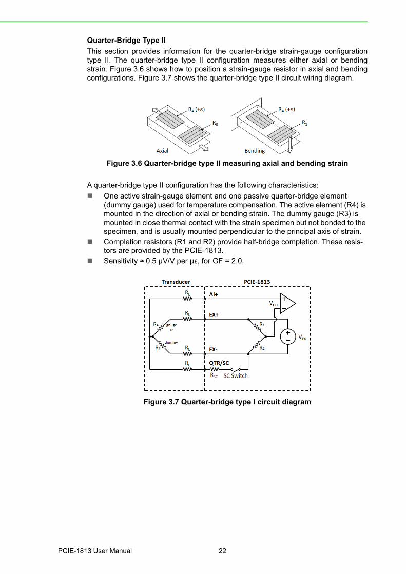
Quarter-Bridge Type IIThis section provides information for the quarter-bridge strain-gauge configurationtype II. The quarter-bridge type II configuration measures either axial or bendingstrain. Figure 3.6 shows how to position a strain-gauge resistor in axial and bendingconfigurations. Figure 3.7 shows the quarter-bridge type II circuit wiring diagram.
Figure 3.6 Quarter-bridge type II measuring axial and bending strain
A quarter-bridge type II configuration has the following characteristics: One active strain-gauge element and one passive quarter-bridge element
(dummy gauge) used for temperature compensation. The active element (R4) is mounted in the direction of axial or bending strain. The dummy gauge (R3) is mounted in close thermal contact with the strain specimen but not bonded to the specimen, and is usually mounted perpendicular to the principal axis of strain.
Completion resistors (R1 and R2) provide half-bridge completion. These resis-tors are provided by the PCIE-1813.
Sensitivity ≈ 0.5 μV/V per με, for GF = 2.0.
Figure 3.7 Quarter-bridge type I circuit diagram

23 PCIE-1813 User Manual
Chapter 3
Signal Connections
Half-Bridge Type IThis section provides information for the half-bridge strain-gauge configuration type I.The half-bridge type I configuration measures either axial or bending strain. Figure3.8 shows how to position a strain-gauge resistor in axial and bending configurations.Figure 3.9 shows the quarter-bridge type II circuit wiring diagram.
Figure 3.8 Half-bridge type I measuring axial and bending strain
A half-bridge type I configuration has the following characteristics: Two active strain-gauge elements. One strain-gauge element is mounted in the
direction of axial strain while the other acts as a Poisson gauge and is mounted perpendicular to the principal axis of strain.
Half-bridge completion resistors (R1 and R2) are provided by the PCIE-1813. Sensitive to both axial and bending strain. Sensitivity ≈ 0.65 μV/V per με, for GF = 2.0.
Figure 3.9 Half-bridge type I circuit diagram
PCIE-1813 User Manual 24
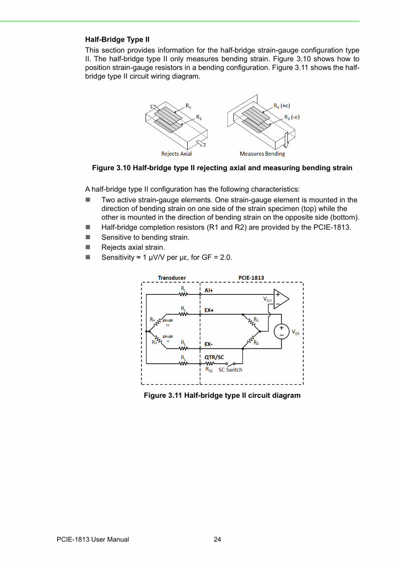
Half-Bridge Type IIThis section provides information for the half-bridge strain-gauge configuration typeII. The half-bridge type II only measures bending strain. Figure 3.10 shows how toposition strain-gauge resistors in a bending configuration. Figure 3.11 shows the half-bridge type II circuit wiring diagram.
Figure 3.10 Half-bridge type II rejecting axial and measuring bending strain
A half-bridge type II configuration has the following characteristics: Two active strain-gauge elements. One strain-gauge element is mounted in the
direction of bending strain on one side of the strain specimen (top) while the other is mounted in the direction of bending strain on the opposite side (bottom).
Half-bridge completion resistors (R1 and R2) are provided by the PCIE-1813. Sensitive to bending strain. Rejects axial strain. Sensitivity ≈ 1 μV/V per με, for GF = 2.0.
Figure 3.11 Half-bridge type II circuit diagram

25 PCIE-1813 User Manual
Chapter 3
Signal Connections
Full-Bridge Type IThis section provides information for the full-bridge strain-gauge configuration type I.The full-bridge type I only measures bending strain. Figure 3.12 shows how to posi-tion strain-gauge resistors in a bending configuration. Figure 3.13 show the full-bridge type I circuit wiring diagram.
Figure 3.12 Full-bridge type I rejecting axial and measuring bending strain
A full-bridge type I configuration has the following characteristics: Four active strain-gauge elements. Two strain-gauge elements are mounted in
the direction of bending strain on one side of the strain specimen (top) while the other two are mounted in the direction of bending strain on the opposite side (bottom).
Highly sensitive to bending strain. Rejects axial strain. Sensitivity ≈ 2 μV/V per με, for GF = 2.0.
Figure 3.13 Full-bridge type I circuit diagram

PCIE-1813 User Manual 26
Full-Bridge Type IIThis section provides information for the full-bridge strain-gauge configuration type II.The full-bridge type II only measures bending strain. Figure 3.14 shows how to posi-tion strain-gauge resistors in a bending configuration. Figure 3.15 show the full-bridge type II circuit wiring diagram.
Figure 3.14 Full-bridge type II rejecting axial and measuring bending strain
A full-bridge type II configuration has the following characteristics: Four active strain-gauge elements. Two strain-gauge elements are mounted in
the direction of bending strain with one on one side of the strain specimen (top) and the other on the opposite side (bottom). The other two act together as a Poisson gauge and are mounted transverse (perpendicular) to the principal axis of strain with one on one side of the strain specimen (top) and the other on the opposite side (bottom).
Sensitive to bending strain. Rejects axial strain. Sensitivity ≈ 1.3 μV/V per με, for GF = 2.0.
Figure 3.15 Full-bridge type II circuit diagram

27 PCIE-1813 User Manual
Chapter 3
Signal Connections
Full-Bridge Type IIIThis section provides information for the full-bridge strain-gauge configuration typeIII. The full-bridge type III only measures axial strain. Figure 3.16 shows how to posi-tion strain-gauge resistors in a bending configuration. Figure 3.17 show the full-bridge type III circuit wiring diagram.
Figure 3.16 Full-bridge type III rejecting axial and measuring bending strain
A full-bridge type III configuration has the following characteristics: Four active strain-gauge elements. Two strain-gauge elements are mounted in
the direction of axial strain with one on one side of the strain specimen (top) and the other on the opposite side (bottom). The other two act together as a Poisson gauge and are mounted transverse (perpendicular) to the principal axis of strain with one on one side of the strain specimen (top) and the other on the opposite side (bottom).
Sensitive to axial strain. Rejects bending strain. Sensitivity ≈ 1.3 μV/V per με, for GF = 2.0.
Figure 3.17 Full-bridge type III circuit diagram

PCIE-1813 User Manual 28
Force, Pressure, and Torque Sensor ConfigurationsThe PCIE-1813 can be used with force sensors (such as load cells), pressure sen-sors, or torque sensors that have the following characteristics: Wheatstone bridge based (Note 1) Unamplified mV/V or V/V output (Note 2)
These sensors typically use a full-bridge configuration with a 350 Ω nominal bridgeresistance, but other configurations and nominal bridge resistances can be used. Fig-ure 3.18 shows the force, pressure, torque sensor circuit diagram.
Figure 3.18 Full-bridge type III circuit diagram
AI Sample Clock Sources Connections Internal AI Sample ClockThe internal AI sample clock uses a 100 MHz time base. Conversions start on the ris-ing edge of the counter output. You can use software to specify the clock source asinternal and the sampling frequency to pace the operation. The minimum frequencyis 0.024 S/s, the maximum frequency is 38.4 KS/s. According to the sampling theory(Nyquist Theorem), you must specify a frequency that is at least twice as fast as theinput’s highest frequency component to achieve a valid sampling. For example, toaccurately sample a 20 kHz signal, you have to specify a sampling frequency of atleast 40 kHz. This consideration can avoid an error condition often know as aliasing,in which high frequency input components appear erroneously as lower frequencieswhen sampling.
29 PCIE-1813 User Manual
Chapter 3
Signal Connections
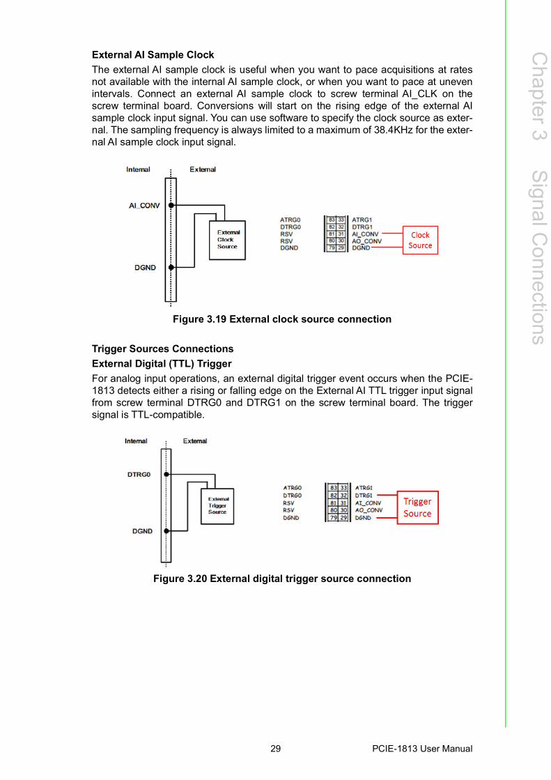
External AI Sample ClockThe external AI sample clock is useful when you want to pace acquisitions at ratesnot available with the internal AI sample clock, or when you want to pace at unevenintervals. Connect an external AI sample clock to screw terminal AI_CLK on thescrew terminal board. Conversions will start on the rising edge of the external AIsample clock input signal. You can use software to specify the clock source as exter-nal. The sampling frequency is always limited to a maximum of 38.4KHz for the exter-nal AI sample clock input signal.
Figure 3.19 External clock source connection
Trigger Sources ConnectionsExternal Digital (TTL) TriggerFor analog input operations, an external digital trigger event occurs when the PCIE-1813 detects either a rising or falling edge on the External AI TTL trigger input signalfrom screw terminal DTRG0 and DTRG1 on the screw terminal board. The triggersignal is TTL-compatible.
Figure 3.20 External digital trigger source connection

PCIE-1813 User Manual 30
Analog Threshold TriggerFor analog input operations, an analog trigger event occurs when the PCIE-1813detects a transition from above a threshold level to below a threshold level (fallingedge), or a transition from below a threshold level to above a threshold level (risingedge). User should connect analog signal from an external device or analog outputchannel on board to external input signal ATRG0 and ATRG1. On the PCIE-1813, thethreshold level is set using a dedicated 16-bit DAC. By software, you can programthe threshold level by writing a voltage value to this DAC; this value can range from -10V to +10V.
Figure 3.21 External analog trigger source connection
Analog Output Connection The PCIE-1813 provides two AO output channels. You can use the internal precision-5 V or -10 V reference to generate 0 to +5 V or 0 to +10 V AO output. Use an exter-nal reference for other AO output ranges. The maximum reference input voltage is±10 V and maximum output scaling is ±10 V. Loading current for AO outputs shouldnot exceed 5 mA. Figure 3.8 shows how to make analog output and external reference input connec-tions on the PCIE-1813.
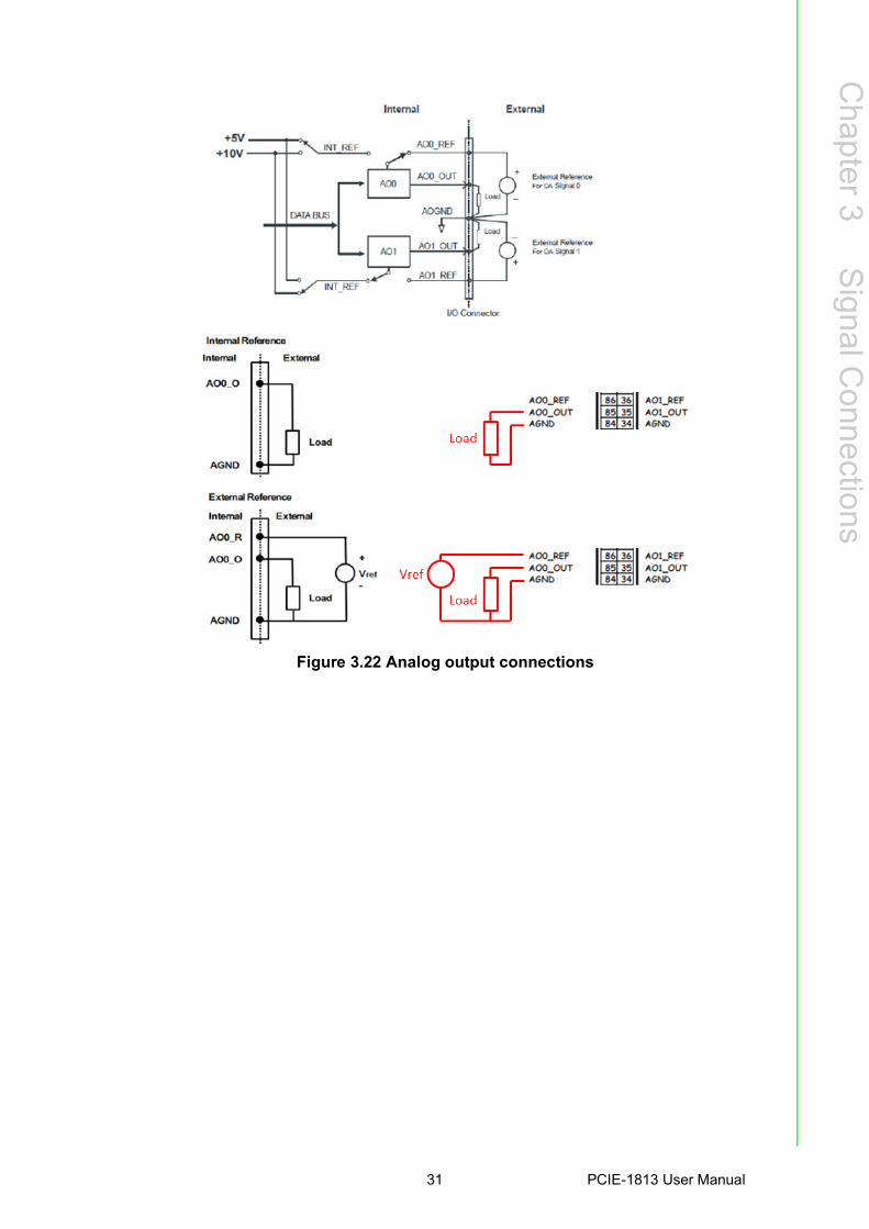
31 PCIE-1813 User Manual
Chapter 3
Signal Connections
Figure 3.22 Analog output connections

PCIE-1813 User Manual 32
AO Sample Clock Sources ConnectionsInternal AO Output ClockThe internal AO output clock applies a 100MHz time base divided by a 32-bit counter.Conversions start on the rising edges of counter output. Through software, user canspecify the clock source and clock frequency to pace the analog output operation.The maximum frequency is 3.030303MS/s.
External AO Output ClockThe external AO output clock is useful when you want to pace analog output opera-tions at rates not available with the internal AO output clock, or when you want topace at uneven intervals. Connect an external AO output clock to the pin and thenthe conversions will start on input signal's rising edge. You can use software to spec-ify the clock source as external. The maximum input clock frequency is 3MS/s.
Figure 3.23 External clock source connection
Trigger Sources ConnectionsExternal Digital (TTL) TriggerThe PCIE-1813 supports external digital (TTL) trigger to activate AO conversions forcontinuous output mode. An external digital trigger event occurs when the PCIE-1813 detects either a rising or falling edge on the External AO TTL trigger input signalfrom the pin of connector. User can define the type of trigger source as rising-edge orfalling-edge by software. The trigger signal is TTL-compatible.
Figure 3.24 External digital trigger source connection

33 PCIE-1813 User Manual
Chapter 3
Signal Connections
3.4.4 Digital Signal Connections The PCIE-1813 has 32 digital input/output channels and they can be configured asinput or output channels. The digital I/O levels are TTL compatible. Digital Input ConnectionsEach digital input channel accepts either dry contact or 0 ~ 5 VDC wet contact inputs.Dry contact capability allows the channel to respond to change in external circuitwhen no voltage exists.
Figure 3.25 Wet and dry contacts
Figure 3.26 Digital input wet signal connection
Figure 3.27 Digital input dry signal connection

PCIE-1813 User Manual 34
Digital Output ConnectionsPCIE-1813 also has TTL digital output.
Figure 3.28 Digital output channel connections
3.5 Field Wiring Considerations When you use PCIE-1813 cards to acquire data from outside, noises in the environ-ment might significantly affect the accuracy of your measurements if due cautions arenot taken. The following measures will be helpful to reduce possible interference run-ning signal wires between signal sources and the PCIE-1813 card.
The signal cables must be kept away from strong electromagnetic sources such as power lines, large electric motors, circuit breakers or welding machines, since they may cause strong electromagnetic interference. Keep the analog sig-nal cables away from any video monitor, since it can significantly affect a data acquisition system.
If the cable travels through an area with significant electromagnetic interference, you should adopt individually shielded, twisted-pair wires as the analog input cable. This type of cable has its signal wires twisted together and shielded with a metal mesh. The metal mesh should only be connected to one point at the sig-nal source ground.
Avoid running the signal cables through any conduit that might have power lines in it.
If you have to place your signal cable parallel to a power line that has a high voltage or high current running through it, try to keep a safe distance between them. Alternatively, you can place the signal cable at a right angle to the power line to minimize the undesirable effect.
The signals transmitted on the cable will be directly affected by the quality of the cable. In order to ensure better signal quality, we recommend that you use PCL-101100R shielded cable.

Appendix AA Specifications

PCIE-1813 User Manual 36
A.1 Function Block

37 PCIE-1813 User Manual
Appendix ASpecifications
A.2 Analog Input
Channels 4 differential, can be enabled/disabled for each channelResolution 26-bitBuild-in memory 1K samplesSampling Rate 38.4 KS/s for each channel
Voltage Input
Input range Bipolar ±10 ±5 ±2.5 ±1.25 ±0.625 ± 0.3125
Absolute accuracyOffset error ±0.1 mVGain error ±0.01% of full-scale range
Temperature driftOffset 25 ppm/ °CGain 15 ppm/ °C
Input Impedance 1GΩ / 350pF Bridge Input
Input Range (V) ±1 V/V ±500 mV/V
±250 mV/V
±125 mV/V
±62.5 mV/V
±31.25 mV/V
Bridge completion Full, half, quarter
Half-bridgeTolerance ±500 μV/V max.Stability 2.5 μV/V per °C max.
Quarter-bridge completion
Values 120 Ω, 350 Ω, 1 kΩ
Tolerance ±0.1% max.
Stability 10 ppm/ °C max.
Shunt Calibration
Values 33.333 kΩ, 50 kΩ, 100 kΩTolerance ±0.1% max.Stability 10 ppm/ °C max.
Excitation char-acteristics
Values120 Ω bridge: 0 ~ +3 V350 Ω bridge: 0 ~ +10 V1 kΩ bridge: 0 ~ +10 V
Tolerance ±2% max.
AccuracyOffset error ±0.1 mVGain error ±0.15% of full-scale range
DriftOffset drift 25 ppm/ °CGain drift 15 ppm/ °C

PCIE-1813 User Manual 38
A.3 Analog Output
A.4 Digital Input/Output
Channels 2
Resolution 16-bit
Memory Size 8K samples
Update Rate 3 MS/s
Output Range Internal Reference 0V~5V, 0V~10V, ±5V, ±10VExternal Reference 0V~xV, -xV~+xV (10 ≤ x ≤ 10)
Accuracy Relative ±1 LSB Differential Non-Linearity ±1 LSB (monotonic)
Slew Rate 20 V/us
Gain Error Adjustable to zero
Drift 30 ppm/ °C
Driving Capability 5 mA
Update Mode static update, waveform
Output Impedance max. 0.1 Ω
Channels 32 (shared)
Input VoltageLow 1.5 V max.High 3.5 V min.
Output VoltageLow 0.5 V max.@ +20 mA (sink)High 4.5 V min.@ -20 mA (source)
Input Load 50KΩ pull-high resistor connect to 5V
Digital Input Filter 1.28 us, 10.24 us, 163.84 us, or 1.31 ms (Each channel individually enable/disable)
Interrupt DI interrupt (rising, falling, or both edge), DI status change detect, DI pat-tern match detect (4 ports independently)

39 PCIE-1813 User Manual
Appendix ASpecifications
A.5 Counter/Timer
A.6 General
Channels 4 channels (independent)Resolution 32-bit
Digital Input Filter 1.28 us, 10.24 us, 163.84 us, or 1.31 ms (Each channel individually enable/disable)
Counter Measurements Event counting, frequency measurement, pulse width measurement
Position Measurements Quadrature encoding (X1, X2, and X4; Channel Z reload), two pulse encod-ing, signed pulse encoding
Output Applications One shot, timer/pulse, pulse width modulation, position comparisonCompatibility * TTL level
Base Clock Internal 20MHz or external clock (10 MHz max.).Selected by software
Output Frequency Max. 10MHz
Clock Input Low 1.5 V max.High 3.5 V min.
Gate Input Low 1.5 V max.High 3.5 V min.
Counter Output Low 0.5 V max. @+15mAHigh 4.5 V min. @-15mA
Error in Advanced Functions
Frequency Mea-surement 0.1% when input signal frequency ≥ 20KHz
Pulse Width Mea-surement 0.1% when input signal frequency ≥ 20KHz
Pulse Output within 2% when output frequency > 20Hz PWM Output within 2% when output frequency > 20Hz
* PCIE-1813 only supports single-ended signal. For differential line driver output encoders,a PCLD-8813 signal conditioning board is required.
Note! When performing advanced functions, like frequency measurement and pulse output, there will be errors. And the error will vary depending on the parameter selections and the OS performance.
I/O Connector Type 100-pin SCSI femaleDimensions 167 x 100 mm (6.57 x 3.93 in)
Power Consumption Typical 3.3 V @ 200 mA, 12 V @ 310 mAMax. 3.3 V @ 450 mA, 12 V @ 650 mA
Temperature Operating 0 ~ 6 0 °C (32 ~ 140 °F) Storage -40 ~ 70 °C (-40 ~ 158 °F)
Relative Humidity Operating 5~85%RH non-condensingStorage 5~95%RH non-condensing
Certifications CE/FCC certified

PCIE-1813 User Manual 40

Appendix BB Operation Theory

PCIE-1813 User Manual 42
B.1 Analog Input Operation This section describes the following features of analog input operation theory thatcan help you realize how to configure the functions and parameters to match variousapplications. AI Hardware Structure Analog input ranges and gains Analog data acquisition mechanism Analog input acquisition modes AI CONV clock source AI trigger sources Analog input data format
B.1.1 AI Hardware Structure The AI conversion hardware structure includes four major parts: PGIA (Programmable Gain Instrument Amplifier) rectifies the input range and
amplify/alleviate input signal to match the input range of A/ D converter. AI converter conceives the rectified voltage from PGIA and transfers it into the
corresponding digital data format. Trigger/Clock control logic enables/disables the whole process and deter-
mines acquisition timing interval.
B.1.2 Analog Input Ranges and Gains The PCIE-1813 can measure bipolar analog input signals. A bipolar signal can rangefrom 0 to ±10 V FSR (Full Scale Range). The PCIE-1813 provides various program-mable gain levels and each channel is allowed to set its own input range individually.Table B.1 lists the effective ranges supported by the PCIE-1813 with gains.
For each channel, choose the gain level providing the most optimal range that canaccommodate the signal range you want to measure.
Table B.1: Gains and Analog Input RangeBipolar Analog Input Range ±10 V ±5 V ±2.5 V ±1.25 V ±0.625 V ±0.3125 V

43 PCIE-1813 User Manual
Appendix BO
peration Theory
B.1.3 AI Trigger ModesThe PCIE-1813 supports four trigger modes and pause function. User can start orstop the operation by trigger mode selection. An extra 24-bit counter is dedicated todelay-trigger mode and about-trigger mode. Figure shows the four different triggermodes.
Start Trigger Acquisition Mode Start trigger acquisition starts when the PCIE-1813 detects the trigger event and stops when you stop the operation. The CONV CLKs before Trigger will be blocked out. You can set post-trigger acquisition mode by software.

PCIE-1813 User Manual 44
Delay to Start Trigger Acquisition Mode In delay to start trigger mode, data acquisition will be activated after a preset delay number of CONV CLKs has been taken after the trigger event. User can set the delay number of CONV CLKs by a 24-bit counter. Delay to start trigger acquisition starts when the PCIE-1813 detects the trigger event and stops when you stop the operation.
Delay to Stop Trigger Acquisition Mode If you want to acquire data after a specific trigger event occurs, then you can take advantage of the delay to stop trigger mode. First designate the size of the allocated memory and the amount of samples to be snatched after the trigger event happens. The about trigger acquisition starts when the first CONV CLK signal comes in. Once a trigger event happens, the on-going data acquisition will continue until the designated amount of CONV CLKs have been reached. When the PCIE-1813 detects the selected about-trigger event, the card keeps acquiring the preset number of samples, and keeps them on the buffer.
Stop Trigger Acquisition Mode Stop trigger mode is a particular application of about-trigger mode. Use pre-trig-ger acquisition mode when you want to acquire data before a specific trigger event occurs. Stop-trigger acquisition starts when you start the operation and stops when the trigger event happens.

45 PCIE-1813 User Manual
Appendix BO
peration Theory
B.1.4 AI CONV Clock Source The PCIE-1813 can adopt both internal and external clock sources to accomplishpacer acquisition. You can set the clock and trigger sources conveniently by soft-ware. The figure can help you understand the routing route of clock and trigger gen-eration.
CONV Clock – Internal AI CONV clock derived from 32-bit divider– External AI CONV clock from terminal board
Internal AI CONV Clock The internal AI CONV clock applies 100 MHz time base accompanied with 32-bit divider. The maximum frequency is 250 KS/s. According to the sampling the-ory (Nyquist Theorem), you must specify a frequency that is at least twice as fast as the input’s highest frequency component to achieve a valid sampling. For example, to accurately sample a 20 kHz signal, you have to specify a sampling frequency of at least 40 kHz. This consideration can avoid an error condition often know as aliasing, in which high frequency input components appear erro-neously as lower frequencies when sampling.
External AI CONV Clock The external AI CONV Clock is convenient in uneven sampling internal. AI con-version will start by each arriving rising edge. The sampling frequency is always limited to a maximum of 250 KHz.
PCIE-1813 User Manual 46
B.1.5 AI Trigger Source The PCIE-1813 supports the following trigger sources for start, delay to start, delay tostop, stop trigger acquisition modes: External digital (TTL) trigger Analog threshold trigger With PCIE-1813, user can also define the type of trigger source as rising-edge or fall-ing-edge. These following sections describe these trigger sources in more detail. External Digital (TTL) Trigger For analog input operations, an external digital trigger event occurs when the PCIE-1813 detects either a rising or falling edge on the External AI TTL trigger input. Thetrigger signal is TTL compatible. Analog Threshold Trigger For analog input operations, an analog trigger event occurs when the PCIE-1813detects a transition from above a threshold level to below a threshold level (fallingedge), or a transition from below a threshold level to above a threshold level (risingedge). User should connect analog signals from external device or analog outputchannel on board to external input signal ATRG0/1. On the PCIE-1813, the thresholdlevel is set using a dedicated 16-bit DAC. By software, you can program the thresh-old level by writing a voltage value to this DAC; this value can range from -10 V to+10 V.
B.2 PCIE-1813 Analog Output Operation The PCIE-1813 card provides two 16-bit multi-range analog output (D/ A) channels.This section describes the following features: Analog output ranges Analog output operation modes Synchronous Analog output waveform AO clock sources AO Trigger sources Analog Output Data Format
Table B.2: Analog Input Data FormatAI Code Mapping Voltage Hex. Dec. Unipolar Bipolar 0000 h 0 d 0 - FS/2 7FFF h 32767 d FS/2 - 1 LSB - 1LSB 8000 h 32768 d FS/2 0 FFFF h 65535 d FS - 1 LSB FS/2 - 1 LSB1 LSB FS/65536 FS/65536
Table B.3: Full-Scale Values for Input Voltage Ranges
Gain Unipolar Bipolar Range FS Range FS
0.5 N/A N/A ± 10 V 20 1 0 ~ 10 V 10 ± 5 V 10 2 0 ~ 5 V 5 ± 2.5 V 5 4 0 ~ 2.5 V 2.5 ± 1.25 V 2.5 8 0 ~ 1.25 V 1.25 ± 0.625 V 1.25

47 PCIE-1813 User Manual
Appendix BO
peration Theory
B.2.1 Analog Output Ranges The PCIE-1813 provides two 16-bit analog output channels, both of which can beconfigured internally to be applicable within 0 ~ 5 V, 0 ~ 10 V, ± 5 V, ± 10 V outputvoltage range. Otherwise, users can use external reference voltage to apply 0 ~ x Vor ± x V output range, where the value x is from -10 to +10. Users can configure theoutput range during driver installation or in software programming.
B.2.2 Analog Output Operation Modes Single Value Operation Mode The single value conversion mode is the simplest way for analog output operation.Users can set the mode of each channel individually. Then users just need to usesoftware to write output data to specific register. The analog output channels will out-put the corresponding voltage immediately. In the single value operation mode, usersneed not set any clock source and trigger source, but only output voltage range. Waveform Mode In waveform mode, all AO channels can change output voltage at the same time.Users can accurately control the update rate (up to 3 MS/s) between conversions ofindividual analog output channels, and takes full advantage of the PCIE-1813. In thismode you can specify a clock and trigger source and either of the two analog outputchannels to work in this mode. Before operating in this mode, users need to set the clock and trigger source first,and then generate the output data stored in the memory buffers of host PC. The hostcomputer then transfers those data to the DACs’ buffers on PCIE-1813. When PCIE-1813 detects a trigger, it outputs the values stored in its buffer. When the buffer’sstorage decreases, the card sends an interrupt request to the host PC which in turnsends samples to the buffer. This output operation will repeat until either all the datais sent from the buffers or until you stop the operation. If the two AO channels areboth operating in continuous output mode, the data in buffer will be sent in an inter-laced manner, i.e. the “Even-Address” samples in the buffer are sent to AO channel0, while the “Odd-Address” samples to AO channel 1.

PCIE-1813 User Manual 48
B.2.3 AO Clock Sources The PCIE-1813 can adopt both internal and external clock sources for pacing theanalog output of each channel: Internal AO output clock with 32-bit Divider External AO output clock from connector
The internal and external AO output clocks are described in more detail as follows: Internal AO Output ClockThe internal AO output clock applies a 100 MHz time base divided by a 32-bitcounter. Conversions start on the rising edges of counter output. Through software,user can specify the clock source and clock frequency to pace the analog outputoperation. The maximum frequency is 3 MS/s. External AO Output Clock The external AO output clock is useful when you want to pace analog output opera-tions at rates not available with the internal AO output clock, or when you want topace at uneven intervals. Connect an external AO output clock to the pin and thenthe conversions will start on input signal’s rising edge. You can use software to spec-ify the clock source as external. The maximum input clock frequency is 3 MS/s.
B.2.4 AO Trigger Sources The PCIE-1813 supports External digital (TTL) trigger to activate AO conversions forwaveform mode. An external digital trigger event occurs when the PCIE-1813 detectseither a rising or falling edge on the External AO TTL trigger input signal from the pinof connector. User can define the type of trigger source as rising-edge or falling-edgeby software. The trigger signal is TTL-compatible.
Table B.4: Analog Output Data FormatAO Code Mapping Voltage Hex. Dec. Unipolar Bipolar 0000 h 0 d 0 - FS/2 7FFF h 32767 d FS/2 - 1 LSB - 1LSB 8000 h 32768 d FS/2 0 FFFF h 65535 d FS - 1 LSB FS/2 - 1 LSB1 LSB FS/65536 FS/65536
Table B.5: Full-Scale Values for Output Voltage RangesReferenceSource
Unipolar Bipolar Range FS Range FS
Internal0 ~ 5 V 5 ± 5 V 10
20 0 ~ 10 V 10 ± 10 V External 0 ~ x V x ± x V 2x

49 PCIE-1813 User Manual
Appendix BO
peration Theory
B.3 Digital Input/Output Operation The PCIE-1813 supports 32 digital I/O channels. You can use each byte as either aninput port or an output port by configuring the corresponding parameter; and all fourchannels of the byte have the same configuration. You do not need to specify the clock source or trigger source. To output the data, youjust need to write it to the digital output channel directly. In the same way, you candirectly read back data from digital input channel. The default configuration afterreset sets all the digital I/O channels to logic-low so users don’t need to worry aboutdamaging external devices during system start up or reset.
B.4 Counter Input and PWM Input/OutputPCIE-1813 offer four 32-bit counters inputs which can perform event counting, fre-quency measurement, pulse width measurement, and encoder counter with compareoutput.Counters on PCIE-1813 have a counter value match interrupt function. When thisinterrupt function is enabled, an interrupt signal will be generated if the counter valuereaches a pre-set counter match value. The counter will continue to count until anoverflow occurs, then it will go back to its reset value zero and continue the countingprocess. A user can set each individual counter channel to count either falling edge(high-to-low) or rising edge (low-to-high) signals.Except measurement functionality, counter input channels can combine with PWMoutput channels to generate single pulse, pulse train or PWM (pulse-width modu-lated) output signal. A pulse-width modulated waveform is created when the Highand Low periods of a periodic rectangular signal are varied. Using PCIE-1813, usercan individually set each PWM channel’s High and Low periods for from 2 to (232 -1)units (1 unit = 50 ns), depending on his needs.1. Event Counter Connection
PCIE-1813 built-in counter can calculate how many pulse are sent into the input channel.

PCIE-1813 User Manual 50
2. Frequency Measurement ConnectionPCIE-1813 built-in counter can measure the frequency value of the signal con-nected to counter input. The measurable maximum frequency is 20 KHz with a frequency error smaller than 1%.
3. Pulse Width Measurement ConnectionPCIE-1813 built-in counter can measure the pulse width value of the signal con-nected to counter input. The measurable range is 50 ns to 107 seconds. You can measure both the logic high time and logic low time within the measurable range.

51 PCIE-1813 User Manual
Appendix BO
peration Theory
4. Pulse Output with Timer InterruptPCIE-1813 counter has internal clock that you can produce periodic output sig-nal with interrupt generated at the same time. PCIE-1813 counter will use inter-nal clock as time base, to fulfill the frequency you want to set. See the figure below as example, the desired frequency is 5 MHz. The internal clock is 20 MHz, so PCIE-1813 will periodically generate output signal and interrupt every 4 pulses of the internal clock. (20 MHz / 5 MHz = 4). Available output frequency range is 0.005 Hz ~ 5 MHz.
5. Delay Pulse Generation Using PCIE-1813 internal clock, you can change the logic level within a specific period, starting from a trigger signal connecting to counter gate input. For exam-ple, if you define the count equals to 3 (as figure below), a counter output will change its status after 3 pulses of internal clock signals pass, after a trigger sig-nal from counter gate becomes high.

PCIE-1813 User Manual 52
6. PWM Output: PCIE-1813 can generate PWM (pulse width modulation) signal which you can configure its logic high time and logic low time as figure below. The available period range for logic high time and logic low time is 100 ns ~ 214 second.
7. Measurements Using Quadrature EncodersThe counters can perform measurements of quadrature encoders that use X1, X2, or X4 encoding. A quadrature encoder can have up to three channels: chan-nels A (Source), B (Aux), and Z (Gate).
– X1 Encoding: When channel A leads channel B in a quadrature cycle, the counter increments. When channel B leads channel A in a quadrature cycle, the counter decrements. The amount of increments and decrements per cycle depends on the type of encoding (X1, X2, or X4).Below figure shows a quadrature cycle and the resulting increments and dec-rements for X1 encoding. When channel A leads channel B, the increment occurs on the rising edge of channel A. When channel B leads channel A, the decrement occurs on the rising edge of channel A.
––––––

53 PCIE-1813 User Manual
Appendix BO
peration Theory
– X2 Encoding: The same behavior holds for X2 encoding except the counter increments or decrements on each edge of channel A, depending on which channel leads the other. Each cycle results in two increments or decrements, as shown in following figure.
– X4 Encoding: Similarly, counter increments or decrements on each edge of channel A and B for X4 encoding. Whether the counter increments or decre-ments depends on which channel leads the other. Each cycle results in four increments or decrements, as shown in below figure.
Some quadrature encoders have a third channel, channel Z, which is also referred to as the index channel. According to the configuration, a rising or falling edge of channel Z causes the counter to be reloaded with a specified value. After the reload occurs, the counter continues to count as before. The following figure illustrates channel Z rising edge reload with X2 encoding.
8. Measurements Using Two Pulse EncodersThe counter supports two pulse encoders that have two channels: channels A (Source) and B (Aux).The counter increments on each active edge of channel A. The counter decre-ments on each active edge of channel B, as shown in below.

PCIE-1813 User Manual 54
9. Measurements Using Signed Pulse EncodersThe counter supports signed pulse encoders that have two channels: channels A (Source) and B (Aux).The counter increments on each active edge of channel A when channel B is low. The counter decrements on each active edge of channel A when channel B is high. This is shown in below.
10. Position ComparisonThis function compares the counter value to a predetermined value. It generates a pulse at Counter Output signal when the counter value becomes equal to the predetermined value. You can define multiple values to be compared and store them in the FIFO. When the counter value becomes equal to the first value in the FIFO, a pulse is generated. In addition, the second value in the FIFO becomes the value to be compared next time.You can program the width of the generated pulse. The range of the pulse width is from 10 ns to 42.94967295 s in step of 10 ns.The following figure shows an example of position comparison using quadratu-reX4 encoding.

55 PCIE-1813 User Manual
Appendix BO
peration Theory

www.advantech.comPlease verify specifications before quoting. This guide is intended for referencepurposes only.All product specifications are subject to change without notice.No part of this publication may be reproduced in any form or by any means,such as electronically, by photocopying, recording or otherwise, without priorwritten permission from the publisher.All brand and product names are trademarks or registered trademarks of theirrespective companies.© Advantech Co., Ltd. 2020