PCG-01014-2.8 © 2018 Intel Corporation....Cyclone® V Device Family Pin Connection Guidelines...
70
Cyclone® V Device Family Pin Connection Guidelines PCG-01014-2.8 Intel recommends that you create a Quartus® Prime design, enter your device I/O assignments, and compile the design. The Quartus Prime design will check your pin connections according to I/O assignments and placement rules. The rules differ from one device to another based on device density, package, I/O assignments, voltage assignments, and other factors that are not fully described in this document or the device handbook. PCG-01014-2.8 © 2018 Intel Corporation. Disclaimer © 2018 Intel Corporation. All rights reserved. Intel, the Intel logo, Altera, Arria, Cyclone, Enpirion, MAX, Megacore, NIOS, Quartus Prime and Stratix words and logos are trademarks of Intel Corporation in the US and/or other countries. Other marks and brands may be claimed as the property of others. Intel warrants performance of its FPGA and semiconductor products to current specifications in accordance with Intel's standard warranty, but reserves the right to make changes to any products and services at any time without notice. Intel assumes no responsibility or liability arising out of the application or use of any information, product, or service described herein except as expressly agreed to in writing by Intel. Intel customers are advised to obtain the latest version of device specifications before relying on any published information and before placing orders for products or services. These pin connection guidelines, and your use thereof, are subject to and governed by Intel’s terms and conditions below. By using these pin connection guidelines, you indicate your acceptance of all such terms and conditions. If you do not agree with such terms and conditions, you may not use the pin connection guidelines, and you are required to promptly and irrevocably destroy the pin connection guidelines and any copies or portions thereof in your possession or under your control. Terms and Conditions: 1. These pin connection guidelines are provided as examples only, and should not be deemed to be technical specifications or recommendations. The use of the pin connection guidelines for any particular design should be verified for device operation with the applicable datasheet and Intel. 2. Subject to these terms and conditions, Intel grants to you the use of these pin connection guidelines as examples of possible pin connections of an Intel programmable logic device-based design. You may not use these pin connection guidelines for any other purpose except as expressly permitted in these terms and conditions. Intel does not recommend, suggest, or require that these pin connection guidelines be used in conjunction or combination with any other software or product, and makes no representations, warranties or guaranties, implied or express as well as any warranties arising from course of performance, course of dealing, or usage in trade including but not limited to the accuracy, completeness or genuineness thereof. 3. Intel will not be liable for any lost revenue, lost profits, or other consequential, indirect, or special damages caused by your use of these pin connection guidelines even if advised of the possibility of such damages occurring. 4. This agreement shall be governed in all respects by the laws of the State of Delaware, without regard to conflict of law or choice of law principles. You agree to submit to the exclusive jurisdiction of the federal and state courts in the State of Delaware for the resolution of any dispute or claim arising out of or relating to these terms of use.
Transcript of PCG-01014-2.8 © 2018 Intel Corporation....Cyclone® V Device Family Pin Connection Guidelines...
Cyclone® V Device Family Pin Connection Guidelines PCG-01014-2.8
Intel recommends that you create a Quartus® Prime design, enter your device I/O assignments, and compile the design. The Quartus Prime design will check your pin connections according to I/O assignments and placement rules. The rules differ from one device to another based on device density, package, I/O assignments, voltage assignments, and other factors that are not fully described in this document or the device handbook.
PCG-01014-2.8 © 2018 Intel Corporation.
Disclaimer © 2018 Intel Corporation. All rights reserved. Intel, the Intel logo, Altera, Arria, Cyclone, Enpirion, MAX, Megacore, NIOS, Quartus Prime and Stratix words and logos are trademarks of Intel Corporation in the US and/or other countries. Other marks and brands may be claimed as the property of others. Intel warrants performance of its FPGA and semiconductor products to current specifications in accordance with Intel's standard warranty, but reserves the right to make changes to any products and services at any time without notice. Intel assumes no responsibility or liability arising out of the application or use of any information, product, or service described herein except as expressly agreed to in writing by Intel. Intel customers are advised to obtain the latest version of device specifications before relying on any published information and before placing orders for products or services.
These pin connection guidelines, and your use thereof, are subject to and governed by Intel’s terms and conditions below. By using these pin connection guidelines, you indicate your acceptance of all such terms and conditions. If you do not agree with such terms and conditions, you may not use the pin connection guidelines, and you are required to promptly and irrevocably destroy the pin connection guidelines and any copies or portions thereof in your possession or under your control.
Terms and Conditions:
1. These pin connection guidelines are provided as examples only, and should not be deemed to be technical specifications or recommendations. The use of the pin connection guidelines for any particular design should be verified for device operation with the applicable datasheet and Intel.
2. Subject to these terms and conditions, Intel grants to you the use of these pin connection guidelines as examples of possible pin connections of an Intel programmable logic device-based design. You may not use these pin connection guidelines for any other purpose except as expressly permitted in these terms and conditions. Intel does not recommend, suggest, or require that these pin connection guidelines be used in conjunction or combination with any other software or product, and makes no representations, warranties or guaranties, implied or express as well as any warranties arising from course of performance, course of dealing, or usage in trade including but not limited to the accuracy, completeness or genuineness thereof.
3. Intel will not be liable for any lost revenue, lost profits, or other consequential, indirect, or special damages caused by your use of these pin connection guidelines even if advised of the possibility of such damages occurring.
4. This agreement shall be governed in all respects by the laws of the State of Delaware, without regard to conflict of law or choice of law principles. You agree to submit to the exclusive jurisdiction of the federal and state courts in the State of Delaware for the resolution of any dispute or claim arising out of or relating to these terms of use.
Cyclone® V Device Family Pin Connection Guidelines PCG-01014-2.8
Intel recommends that you create a Quartus® Prime design, enter your device I/O assignments, and compile the design. The Quartus Prime design will check your pin connections according to I/O assignments and placement rules. The rules differ from one device to another based on device density, package, I/O assignments, voltage assignments, and other factors that are not fully described in this document or the device handbook.
PCG-01014-2.8 © 2018 Intel Corporation.
Pin Connection Guidelines
Cyclone V Pin Name Pin Type (1st
and 2nd Function)
Pin Description Connection Guidelines
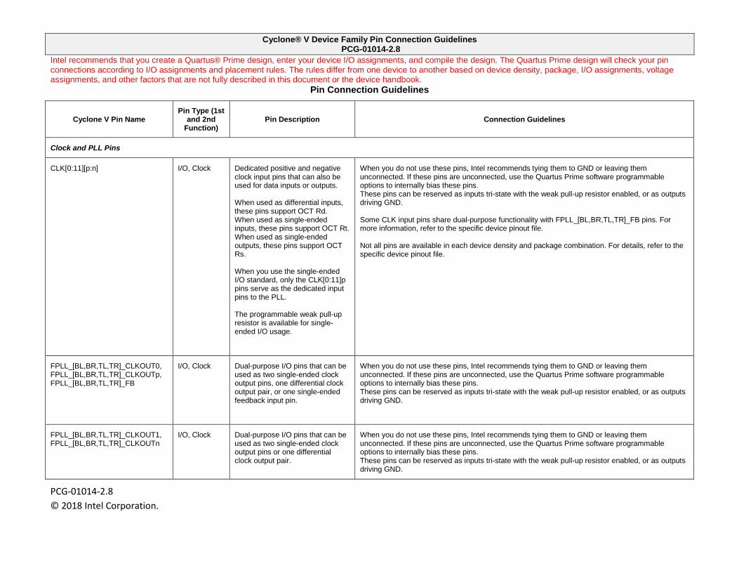
Clock and PLL Pins
CLK[0:11][p:n] I/O, Clock Dedicated positive and negative clock input pins that can also be used for data inputs or outputs. When used as differential inputs, these pins support OCT Rd. When used as single-ended inputs, these pins support OCT Rt. When used as single-ended outputs, these pins support OCT Rs. When you use the single-ended I/O standard, only the CLK[0:11]p pins serve as the dedicated input pins to the PLL. The programmable weak pull-up resistor is available for single-ended I/O usage.
When you do not use these pins, Intel recommends tying them to GND or leaving them unconnected. If these pins are unconnected, use the Quartus Prime software programmable options to internally bias these pins. These pins can be reserved as inputs tri-state with the weak pull-up resistor enabled, or as outputs driving GND. Some CLK input pins share dual-purpose functionality with FPLL_[BL,BR,TL,TR]_FB pins. For more information, refer to the specific device pinout file. Not all pins are available in each device density and package combination. For details, refer to the specific device pinout file.
FPLL_[BL,BR,TL,TR]_CLKOUT0, FPLL_[BL,BR,TL,TR]_CLKOUTp, FPLL_[BL,BR,TL,TR]_FB
I/O, Clock Dual-purpose I/O pins that can be used as two single-ended clock output pins, one differential clock output pair, or one single-ended feedback input pin.
When you do not use these pins, Intel recommends tying them to GND or leaving them unconnected. If these pins are unconnected, use the Quartus Prime software programmable options to internally bias these pins. These pins can be reserved as inputs tri-state with the weak pull-up resistor enabled, or as outputs driving GND.
FPLL_[BL,BR,TL,TR]_CLKOUT1, FPLL_[BL,BR,TL,TR]_CLKOUTn
I/O, Clock Dual-purpose I/O pins that can be used as two single-ended clock output pins or one differential clock output pair.
When you do not use these pins, Intel recommends tying them to GND or leaving them unconnected. If these pins are unconnected, use the Quartus Prime software programmable options to internally bias these pins. These pins can be reserved as inputs tri-state with the weak pull-up resistor enabled, or as outputs driving GND.
Cyclone® V Device Family Pin Connection Guidelines PCG-01014-2.8
Intel recommends that you create a Quartus® Prime design, enter your device I/O assignments, and compile the design. The Quartus Prime design will check your pin connections according to I/O assignments and placement rules. The rules differ from one device to another based on device density, package, I/O assignments, voltage assignments, and other factors that are not fully described in this document or the device handbook.
PCG-01014-2.8 © 2018 Intel Corporation.
Cyclone V Pin Name Pin Type (1st
and 2nd Function)
Pin Description Connection Guidelines
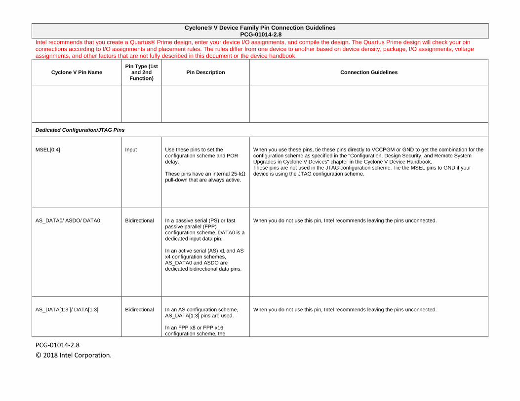
Dedicated Configuration/JTAG Pins
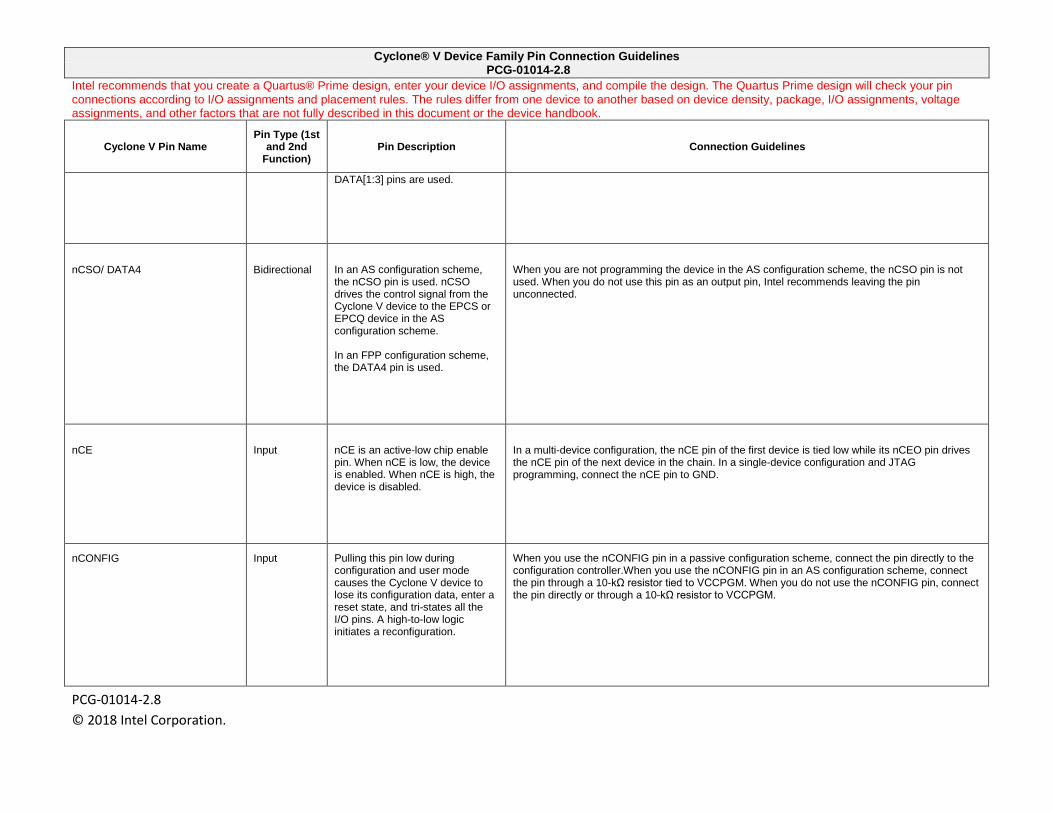
MSEL[0:4] Input Use these pins to set the configuration scheme and POR delay. These pins have an internal 25-kΩ pull-down that are always active.
When you use these pins, tie these pins directly to VCCPGM or GND to get the combination for the configuration scheme as specified in the "Configuration, Design Security, and Remote System Upgrades in Cyclone V Devices" chapter in the Cyclone V Device Handbook. These pins are not used in the JTAG configuration scheme. Tie the MSEL pins to GND if your device is using the JTAG configuration scheme.
AS_DATA0/ ASDO/ DATA0 Bidirectional In a passive serial (PS) or fast passive parallel (FPP) configuration scheme, DATA0 is a dedicated input data pin. In an active serial (AS) x1 and AS x4 configuration schemes, AS_DATA0 and ASDO are dedicated bidirectional data pins.
When you do not use this pin, Intel recommends leaving the pins unconnected.
AS_DATA[1:3 ]/ DATA[1:3] Bidirectional In an AS configuration scheme, AS_DATA[1:3] pins are used. In an FPP x8 or FPP x16 configuration scheme, the
When you do not use this pin, Intel recommends leaving the pins unconnected.
Cyclone® V Device Family Pin Connection Guidelines PCG-01014-2.8
Intel recommends that you create a Quartus® Prime design, enter your device I/O assignments, and compile the design. The Quartus Prime design will check your pin connections according to I/O assignments and placement rules. The rules differ from one device to another based on device density, package, I/O assignments, voltage assignments, and other factors that are not fully described in this document or the device handbook.
PCG-01014-2.8 © 2018 Intel Corporation.
Cyclone V Pin Name Pin Type (1st
and 2nd Function)
Pin Description Connection Guidelines
DATA[1:3] pins are used.
nCSO/ DATA4 Bidirectional In an AS configuration scheme, the nCSO pin is used. nCSO drives the control signal from the Cyclone V device to the EPCS or EPCQ device in the AS configuration scheme. In an FPP configuration scheme, the DATA4 pin is used.
When you are not programming the device in the AS configuration scheme, the nCSO pin is not used. When you do not use this pin as an output pin, Intel recommends leaving the pin unconnected.
nCE Input nCE is an active-low chip enable pin. When nCE is low, the device is enabled. When nCE is high, the device is disabled.
In a multi-device configuration, the nCE pin of the first device is tied low while its nCEO pin drives the nCE pin of the next device in the chain. In a single-device configuration and JTAG programming, connect the nCE pin to GND.
nCONFIG Input Pulling this pin low during configuration and user mode causes the Cyclone V device to lose its configuration data, enter a reset state, and tri-states all the I/O pins. A high-to-low logic initiates a reconfiguration.
When you use the nCONFIG pin in a passive configuration scheme, connect the pin directly to the configuration controller.When you use the nCONFIG pin in an AS configuration scheme, connect the pin through a 10-kΩ resistor tied to VCCPGM. When you do not use the nCONFIG pin, connect the pin directly or through a 10-kΩ resistor to VCCPGM.
Cyclone® V Device Family Pin Connection Guidelines PCG-01014-2.8
Intel recommends that you create a Quartus® Prime design, enter your device I/O assignments, and compile the design. The Quartus Prime design will check your pin connections according to I/O assignments and placement rules. The rules differ from one device to another based on device density, package, I/O assignments, voltage assignments, and other factors that are not fully described in this document or the device handbook.
PCG-01014-2.8 © 2018 Intel Corporation.
Cyclone V Pin Name Pin Type (1st
and 2nd Function)
Pin Description Connection Guidelines
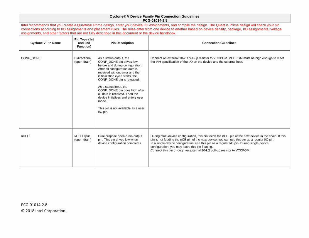
CONF_DONE Bidirectional (open-drain)
As a status output, the CONF_DONE pin drives low before and during configuration. After all configuration data is received without error and the initialization cycle starts, the CONF_DONE pin is released. As a status input, the CONF_DONE pin goes high after all data is received. Then the device initializes and enters user mode. This pin is not available as a user I/O pin.
Connect an external 10-kΩ pull-up resistor to VCCPGM. VCCPGM must be high enough to meet the VIH specification of the I/O on the device and the external host.
nCEO I/O, Output (open-drain)
Dual-purpose open-drain output pin. This pin drives low when device configuration completes.
During multi-device configuration, this pin feeds the nCE pin of the next device in the chain. If this pin is not feeding the nCE pin of the next device, you can use this pin as a regular I/O pin. In a single-device configuration, use this pin as a regular I/O pin. During single-device configuration, you may leave this pin floating. Connect this pin through an external 10-kΩ pull-up resistor to VCCPGM.
Cyclone® V Device Family Pin Connection Guidelines PCG-01014-2.8
Intel recommends that you create a Quartus® Prime design, enter your device I/O assignments, and compile the design. The Quartus Prime design will check your pin connections according to I/O assignments and placement rules. The rules differ from one device to another based on device density, package, I/O assignments, voltage assignments, and other factors that are not fully described in this document or the device handbook.
PCG-01014-2.8 © 2018 Intel Corporation.
Cyclone V Pin Name Pin Type (1st
and 2nd Function)
Pin Description Connection Guidelines
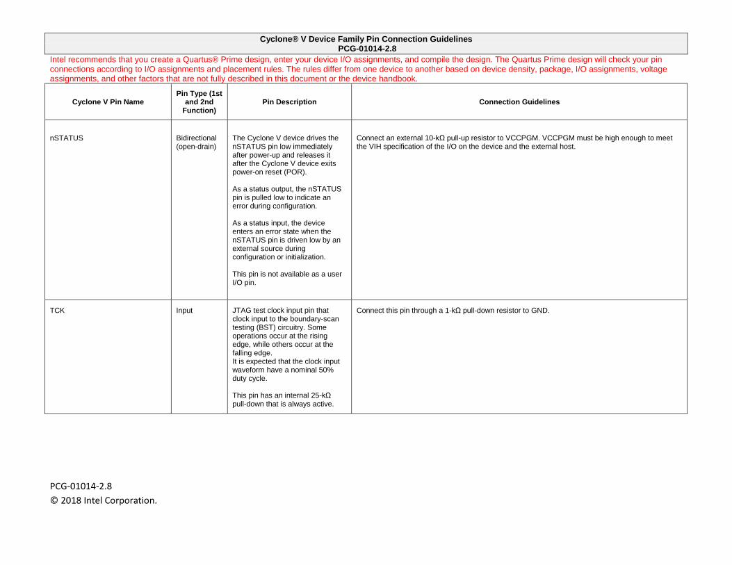
nSTATUS Bidirectional (open-drain)
The Cyclone V device drives the nSTATUS pin low immediately after power-up and releases it after the Cyclone V device exits power-on reset (POR). As a status output, the nSTATUS pin is pulled low to indicate an error during configuration. As a status input, the device enters an error state when the nSTATUS pin is driven low by an external source during configuration or initialization. This pin is not available as a user I/O pin.
Connect an external 10-kΩ pull-up resistor to VCCPGM. VCCPGM must be high enough to meet the VIH specification of the I/O on the device and the external host.
TCK Input JTAG test clock input pin that clock input to the boundary-scan testing (BST) circuitry. Some operations occur at the rising edge, while others occur at the falling edge. It is expected that the clock input waveform have a nominal 50% duty cycle. This pin has an internal 25-kΩ pull-down that is always active.
Connect this pin through a 1-kΩ pull-down resistor to GND.
Cyclone® V Device Family Pin Connection Guidelines PCG-01014-2.8
Intel recommends that you create a Quartus® Prime design, enter your device I/O assignments, and compile the design. The Quartus Prime design will check your pin connections according to I/O assignments and placement rules. The rules differ from one device to another based on device density, package, I/O assignments, voltage assignments, and other factors that are not fully described in this document or the device handbook.
PCG-01014-2.8 © 2018 Intel Corporation.
Cyclone V Pin Name Pin Type (1st
and 2nd Function)
Pin Description Connection Guidelines
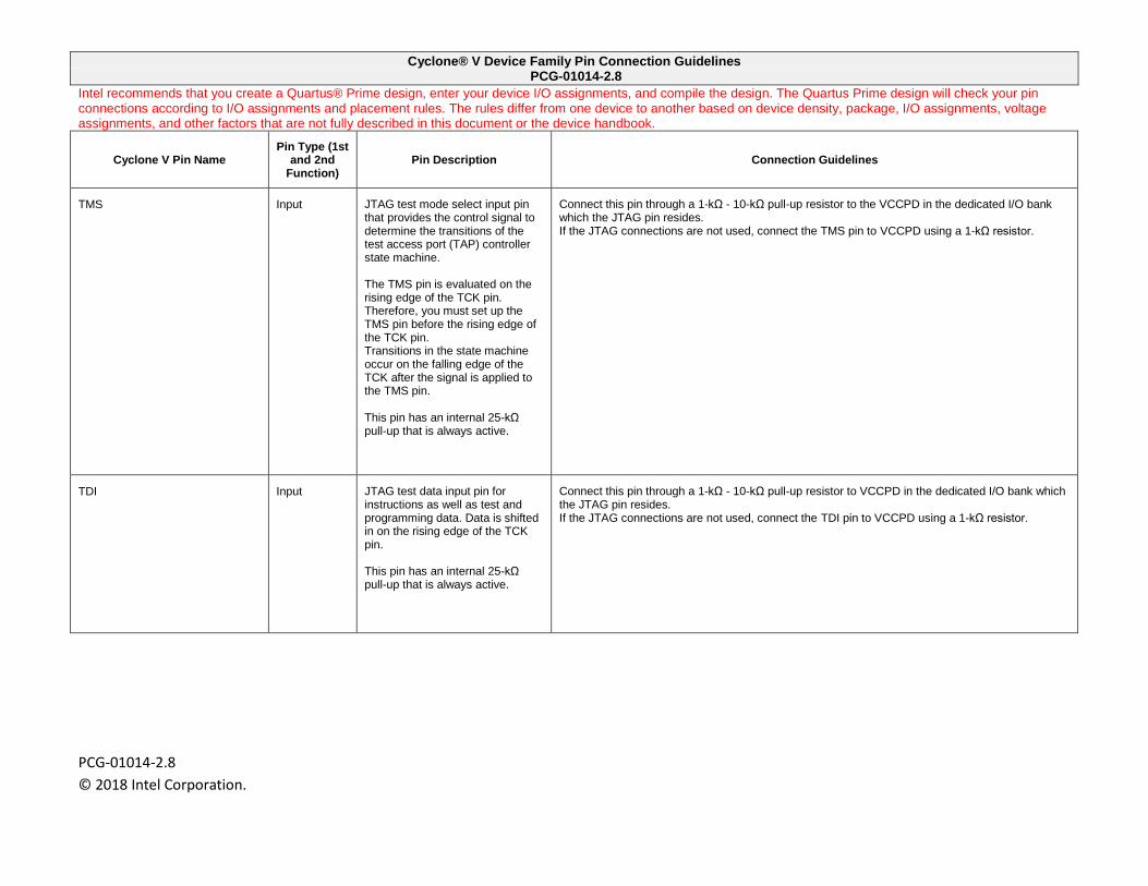
TMS Input JTAG test mode select input pin that provides the control signal to determine the transitions of the test access port (TAP) controller state machine. The TMS pin is evaluated on the rising edge of the TCK pin. Therefore, you must set up the TMS pin before the rising edge of the TCK pin. Transitions in the state machine occur on the falling edge of the TCK after the signal is applied to the TMS pin. This pin has an internal 25-kΩ pull-up that is always active.
Connect this pin through a 1-kΩ - 10-kΩ pull-up resistor to the VCCPD in the dedicated I/O bank which the JTAG pin resides. If the JTAG connections are not used, connect the TMS pin to VCCPD using a 1-kΩ resistor.
TDI Input JTAG test data input pin for instructions as well as test and programming data. Data is shifted in on the rising edge of the TCK pin. This pin has an internal 25-kΩ pull-up that is always active.
Connect this pin through a 1-kΩ - 10-kΩ pull-up resistor to VCCPD in the dedicated I/O bank which the JTAG pin resides. If the JTAG connections are not used, connect the TDI pin to VCCPD using a 1-kΩ resistor.
Cyclone® V Device Family Pin Connection Guidelines PCG-01014-2.8
Intel recommends that you create a Quartus® Prime design, enter your device I/O assignments, and compile the design. The Quartus Prime design will check your pin connections according to I/O assignments and placement rules. The rules differ from one device to another based on device density, package, I/O assignments, voltage assignments, and other factors that are not fully described in this document or the device handbook.
PCG-01014-2.8 © 2018 Intel Corporation.
Cyclone V Pin Name Pin Type (1st
and 2nd Function)
Pin Description Connection Guidelines
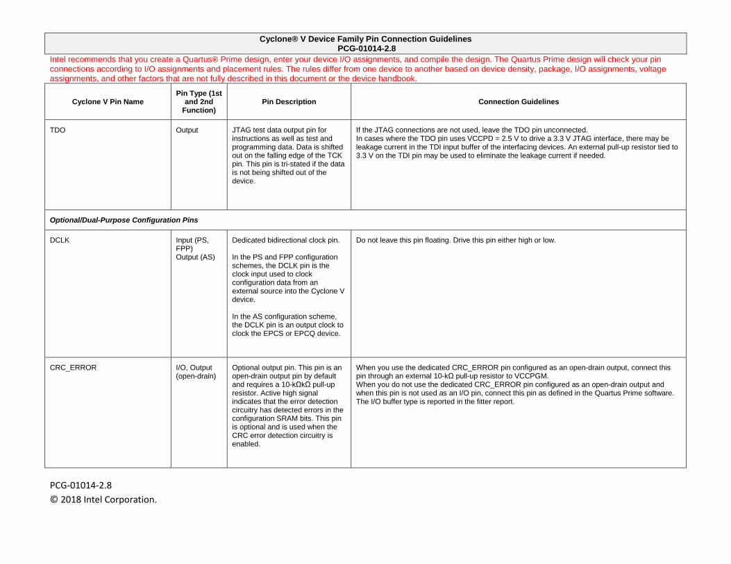
TDO Output JTAG test data output pin for instructions as well as test and programming data. Data is shifted out on the falling edge of the TCK pin. This pin is tri-stated if the data is not being shifted out of the device.
If the JTAG connections are not used, leave the TDO pin unconnected. In cases where the TDO pin uses VCCPD = 2.5 V to drive a 3.3 V JTAG interface, there may be leakage current in the TDI input buffer of the interfacing devices. An external pull-up resistor tied to 3.3 V on the TDI pin may be used to eliminate the leakage current if needed.
Optional/Dual-Purpose Configuration Pins
DCLK Input (PS, FPP) Output (AS)
Dedicated bidirectional clock pin. In the PS and FPP configuration schemes, the DCLK pin is the clock input used to clock configuration data from an external source into the Cyclone V device. In the AS configuration scheme, the DCLK pin is an output clock to clock the EPCS or EPCQ device.
Do not leave this pin floating. Drive this pin either high or low.
CRC_ERROR I/O, Output (open-drain)
Optional output pin. This pin is an open-drain output pin by default and requires a 10-kΩkΩ pull-up resistor. Active high signal indicates that the error detection circuitry has detected errors in the configuration SRAM bits. This pin is optional and is used when the CRC error detection circuitry is enabled.
When you use the dedicated CRC_ERROR pin configured as an open-drain output, connect this pin through an external 10-kΩ pull-up resistor to VCCPGM. When you do not use the dedicated CRC_ERROR pin configured as an open-drain output and when this pin is not used as an I/O pin, connect this pin as defined in the Quartus Prime software. The I/O buffer type is reported in the fitter report.
Cyclone® V Device Family Pin Connection Guidelines PCG-01014-2.8
Intel recommends that you create a Quartus® Prime design, enter your device I/O assignments, and compile the design. The Quartus Prime design will check your pin connections according to I/O assignments and placement rules. The rules differ from one device to another based on device density, package, I/O assignments, voltage assignments, and other factors that are not fully described in this document or the device handbook.
PCG-01014-2.8 © 2018 Intel Corporation.
Cyclone V Pin Name Pin Type (1st
and 2nd Function)
Pin Description Connection Guidelines
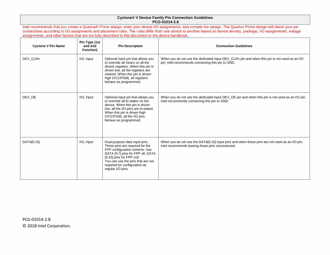
DEV_CLRn I/O, Input Optional input pin that allows you to override all clears on all the device registers. When this pin is driven low, all the registers are cleared. When this pin is driven high (VCCPGM), all registers behave as programmed.
When you do not use the dedicated input DEV_CLRn pin and when this pin is not used as an I/O pin, Intel recommends connecting this pin to GND.
DEV_OE I/O, Input Optional input pin that allows you to override all tri-states on the device. When this pin is driven low, all the I/O pins are tri-stated. When this pin is driven high (VCCPGM), all the I/O pins behave as programmed.
When you do not use the dedicated input DEV_OE pin and when this pin is not used as an I/O pin, Intel recommends connecting this pin to GND.
DATA[5:15] I/O, Input Dual-purpose data input pins. These pins are required for the FPP configuration scheme. Use DATA [5:7] pins for FPP x8, DATA [5:15] pins for FPP x16. You can use the pins that are not required for configuration as regular I/O pins.
When you do not use the DATA[5:15] input pins and when these pins are not used as an I/O pin, Intel recommends leaving these pins unconnected.
Cyclone® V Device Family Pin Connection Guidelines PCG-01014-2.8
Intel recommends that you create a Quartus® Prime design, enter your device I/O assignments, and compile the design. The Quartus Prime design will check your pin connections according to I/O assignments and placement rules. The rules differ from one device to another based on device density, package, I/O assignments, voltage assignments, and other factors that are not fully described in this document or the device handbook.
PCG-01014-2.8 © 2018 Intel Corporation.
Cyclone V Pin Name Pin Type (1st
and 2nd Function)
Pin Description Connection Guidelines
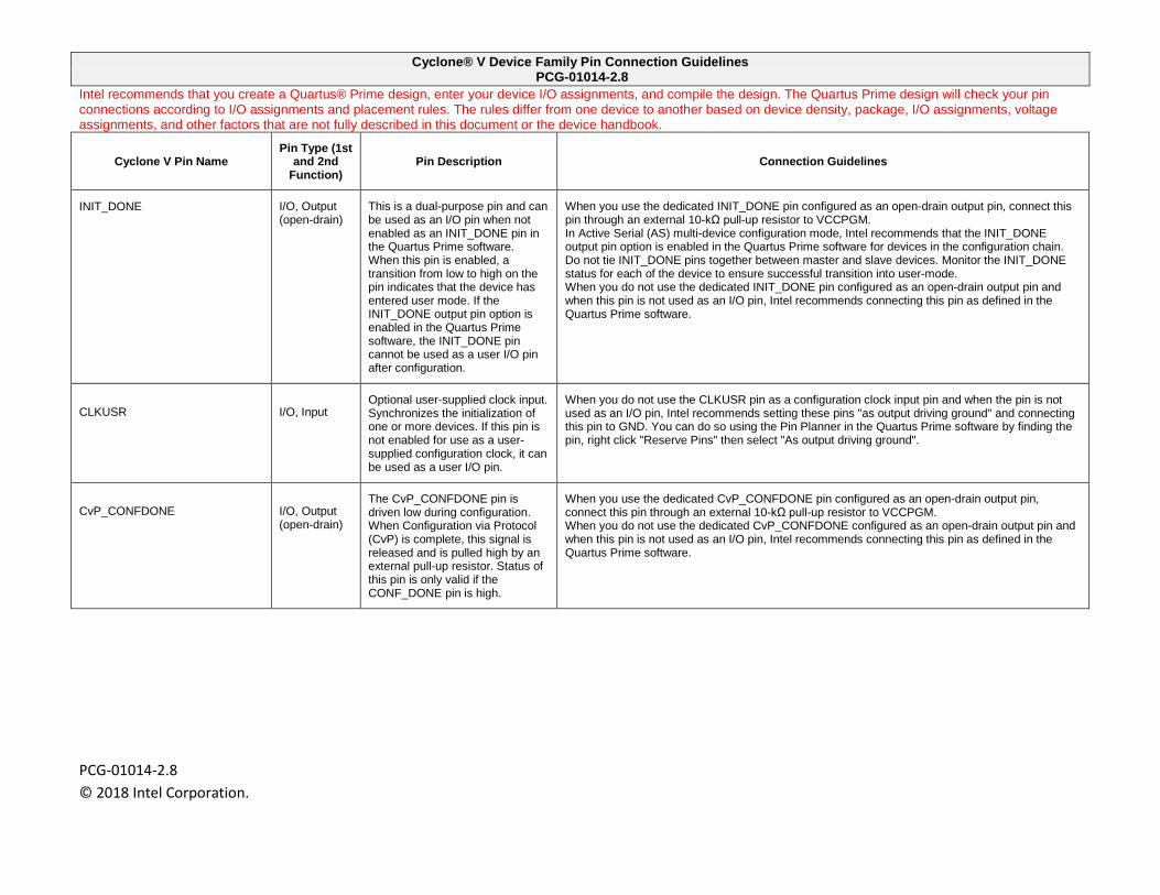
INIT_DONE I/O, Output (open-drain)
This is a dual-purpose pin and can be used as an I/O pin when not enabled as an INIT_DONE pin in the Quartus Prime software. When this pin is enabled, a transition from low to high on the pin indicates that the device has entered user mode. If the INIT_DONE output pin option is enabled in the Quartus Prime software, the INIT_DONE pin cannot be used as a user I/O pin after configuration.
When you use the dedicated INIT_DONE pin configured as an open-drain output pin, connect this pin through an external 10-kΩ pull-up resistor to VCCPGM. In Active Serial (AS) multi-device configuration mode, Intel recommends that the INIT_DONE output pin option is enabled in the Quartus Prime software for devices in the configuration chain. Do not tie INIT_DONE pins together between master and slave devices. Monitor the INIT_DONE status for each of the device to ensure successful transition into user-mode. When you do not use the dedicated INIT_DONE pin configured as an open-drain output pin and when this pin is not used as an I/O pin, Intel recommends connecting this pin as defined in the Quartus Prime software.
CLKUSR I/O, Input Optional user-supplied clock input. Synchronizes the initialization of one or more devices. If this pin is not enabled for use as a user-supplied configuration clock, it can be used as a user I/O pin.
When you do not use the CLKUSR pin as a configuration clock input pin and when the pin is not used as an I/O pin, Intel recommends setting these pins "as output driving ground" and connecting this pin to GND. You can do so using the Pin Planner in the Quartus Prime software by finding the pin, right click "Reserve Pins" then select "As output driving ground".
CvP_CONFDONE I/O, Output (open-drain)
The CvP_CONFDONE pin is driven low during configuration. When Configuration via Protocol (CvP) is complete, this signal is released and is pulled high by an external pull-up resistor. Status of this pin is only valid if the CONF_DONE pin is high.
When you use the dedicated CvP_CONFDONE pin configured as an open-drain output pin, connect this pin through an external 10-kΩ pull-up resistor to VCCPGM. When you do not use the dedicated CvP_CONFDONE configured as an open-drain output pin and when this pin is not used as an I/O pin, Intel recommends connecting this pin as defined in the Quartus Prime software.
Cyclone® V Device Family Pin Connection Guidelines PCG-01014-2.8
Intel recommends that you create a Quartus® Prime design, enter your device I/O assignments, and compile the design. The Quartus Prime design will check your pin connections according to I/O assignments and placement rules. The rules differ from one device to another based on device density, package, I/O assignments, voltage assignments, and other factors that are not fully described in this document or the device handbook.
PCG-01014-2.8 © 2018 Intel Corporation.
Cyclone V Pin Name Pin Type (1st
and 2nd Function)
Pin Description Connection Guidelines
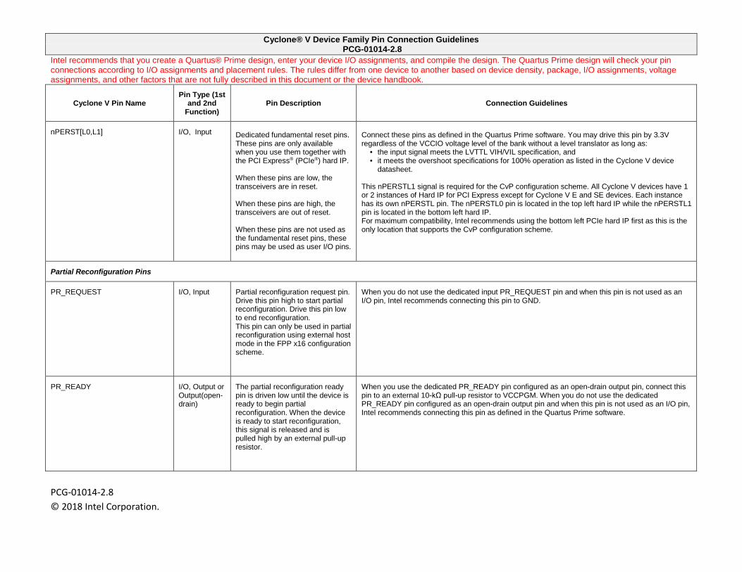
nPERST[L0,L1] I/O, Input Dedicated fundamental reset pins. These pins are only available when you use them together with the PCI Express® (PCIe®) hard IP. When these pins are low, the transceivers are in reset. When these pins are high, the transceivers are out of reset. When these pins are not used as the fundamental reset pins, these pins may be used as user I/O pins.
Connect these pins as defined in the Quartus Prime software. You may drive this pin by 3.3V regardless of the VCCIO voltage level of the bank without a level translator as long as:
• the input signal meets the LVTTL VIH/VIL specification, and • it meets the overshoot specifications for 100% operation as listed in the Cyclone V device
datasheet.
This nPERSTL1 signal is required for the CvP configuration scheme. All Cyclone V devices have 1 or 2 instances of Hard IP for PCI Express except for Cyclone V E and SE devices. Each instance has its own nPERSTL pin. The nPERSTL0 pin is located in the top left hard IP while the nPERSTL1 pin is located in the bottom left hard IP. For maximum compatibility, Intel recommends using the bottom left PCIe hard IP first as this is the only location that supports the CvP configuration scheme.
Partial Reconfiguration Pins
PR_REQUEST I/O, Input Partial reconfiguration request pin. Drive this pin high to start partial reconfiguration. Drive this pin low to end reconfiguration. This pin can only be used in partial reconfiguration using external host mode in the FPP x16 configuration scheme.
When you do not use the dedicated input PR_REQUEST pin and when this pin is not used as an I/O pin, Intel recommends connecting this pin to GND.
PR_READY I/O, Output or Output(open-drain)
The partial reconfiguration ready pin is driven low until the device is ready to begin partial reconfiguration. When the device is ready to start reconfiguration, this signal is released and is pulled high by an external pull-up resistor.
When you use the dedicated PR_READY pin configured as an open-drain output pin, connect this pin to an external 10-kΩ pull-up resistor to VCCPGM. When you do not use the dedicated PR_READY pin configured as an open-drain output pin and when this pin is not used as an I/O pin, Intel recommends connecting this pin as defined in the Quartus Prime software.
Cyclone® V Device Family Pin Connection Guidelines PCG-01014-2.8
Intel recommends that you create a Quartus® Prime design, enter your device I/O assignments, and compile the design. The Quartus Prime design will check your pin connections according to I/O assignments and placement rules. The rules differ from one device to another based on device density, package, I/O assignments, voltage assignments, and other factors that are not fully described in this document or the device handbook.
PCG-01014-2.8 © 2018 Intel Corporation.
Cyclone V Pin Name Pin Type (1st
and 2nd Function)
Pin Description Connection Guidelines
PR_ERROR I/O, Output, or Output (open-drain)
The partial reconfiguration error pin is driven low during partial reconfiguration unless the device detects an error. If an error is detected, this signal is released and pulled high by an external pull-up resistor.
When you use the dedicated PR_ERROR pin configured as an open-drain output pin, connect this pin through an external 10-kΩ pull-up resistor to VCCPGM. When you do not use the dedicated PR_ERROR pin configured as an open-drain output pin and when this pin is not used as an I/O pin, Intel recommends connecting this pin as defined in the Quartus Prime software.
PR_DONE I/O, Output or Output (open-drain)
The partial reconfiguration done pin is driven low until the partial reconfiguration is complete. When the reconfiguration is complete, this signal is released and is pulled high by an external pull-up resistor.
When you use the dedicated PR_DONE pin configured as an open-drain output pin, connect this pin through an external 10-kΩ pull-up resistor to VCCPGM. When you do not use the dedicated PR_DONE configured as an open-drain output pin and when this pin is not used as an I/O pin, Intel recommends connecting this pin as defined in the Quartus Prime software.
Differential I/O Pins
DIFFIO_RX_[B,T,R][#:#]p, DIFFIO_RX_[B,T,R][#:#]n
I/O, RX channel
These are true LVDS receiver channels on row and column I/O banks. Pins with a "p" suffix carry the positive signal for the differential channel. Pins with an "n" suffix carry the negative signal for the differential channel. If not used for differential signaling, these pins are available as user I/O pins. OCT Rd is supported on all the DIFFIO_RX pins.
Connect unused pins as defined in the Quartus Prime software.
For design compiled with Quartus II 13.1 onwards, refer to KDB - rd10102013_979 for guideline in reducing percentage of crosstalk and Simulatneous Switching Noise (SSN).
Cyclone® V Device Family Pin Connection Guidelines PCG-01014-2.8
Intel recommends that you create a Quartus® Prime design, enter your device I/O assignments, and compile the design. The Quartus Prime design will check your pin connections according to I/O assignments and placement rules. The rules differ from one device to another based on device density, package, I/O assignments, voltage assignments, and other factors that are not fully described in this document or the device handbook.
PCG-01014-2.8 © 2018 Intel Corporation.
Cyclone V Pin Name Pin Type (1st
and 2nd Function)
Pin Description Connection Guidelines
DIFFIO_TX_[B,T,R][#:#]p, DIFFIO_TX_[B,T,R][#:#]n
I/O, TX channel
These are true LVDS transmitter channels on row and column I/O banks. Pins with a "p" suffix carry the positive signal for the differential channel. Pins with an "n" suffix carry the negative signal for the differential channel. If not used for differential signaling, these pins are available as user I/O pins.
Connect unused pins as defined in the Quartus Prime software.
For design compiled with Quartus II 13.1 onwards, refer to KDB - rd10102013_979 for guideline in reducing percentage of crosstalk and Simulatneous Switching Noise (SSN).
DIFFOUT_[B,T,R][#:#]p, DIFFOUT_[B,T,R][#:#]n
I/O, TX channel
These are emulated LVDS output channels. All the user I/Os, including I/Os with true LVDS input buffers, can be configured as emulated LVDS output buffers. External resistor network is needed for emulated LVDS output buffers. Pins with a "p" suffix carry the positive signal for the differential channel. Pins with an "n" suffix carry the negative signal for the differential channel. If not used for differential signaling, these pins are available as user I/O pins.
Connect unused pins as defined in the Quartus Prime software.
For design compiled with Quartus II 13.1 onwards, refer to KDB - rd10102013_979 for guideline in reducing percentage of crosstalk and Simulatneous Switching Noise (SSN).
External Memory Interface Pins
DQS[#][B,R,T] I/O, bidirectional
Optional data strobe signal for use in external memory interfacing. These pins drive to dedicated DQS phase shift circuitry. The shifted DQS signal can also drive
Connect unused pins as defined in the Quartus Prime software.
Cyclone® V Device Family Pin Connection Guidelines PCG-01014-2.8
Intel recommends that you create a Quartus® Prime design, enter your device I/O assignments, and compile the design. The Quartus Prime design will check your pin connections according to I/O assignments and placement rules. The rules differ from one device to another based on device density, package, I/O assignments, voltage assignments, and other factors that are not fully described in this document or the device handbook.
PCG-01014-2.8 © 2018 Intel Corporation.
Cyclone V Pin Name Pin Type (1st
and 2nd Function)
Pin Description Connection Guidelines
to internal logic.
DQSn[#][B,R,T] I/O, bidirectional
Optional complementary data strobe signal for use in external memory interfacing. These pins drive to dedicated DQS phase shift circuitry.
Connect unused pins as defined in the Quartus Prime software.
DQ[#][B,R,T] I/O, bidirectional
Optional data signal for use in external memory interfacing. The order of the DQ bits within a designated DQ bus is not important; however, use caution when making pin assignments if you plan on migrating to a different memory interface that has a different DQ bus width. Analyze the available DQ pins across all pertinent DQS columns in the pin list.
Connect unused pins as defined in the Quartus Prime software.
Hard Memory PHY Pins
[B,T]_DQS_[#] I/O, bidirectional
Optional data strobe signal for use in external memory interfacing. These pins drive to dedicated DQS phase shift circuitry. The shifted DQS signal can also drive to internal logic.
If hard memory PHY is used, connection to memory device DQS pin must start from [B,T]_DQS_0 pin. For details, refer to the specific device pinout file. Connect unused pins as defined in the Quartus Prime software.
Cyclone® V Device Family Pin Connection Guidelines PCG-01014-2.8
Intel recommends that you create a Quartus® Prime design, enter your device I/O assignments, and compile the design. The Quartus Prime design will check your pin connections according to I/O assignments and placement rules. The rules differ from one device to another based on device density, package, I/O assignments, voltage assignments, and other factors that are not fully described in this document or the device handbook.
PCG-01014-2.8 © 2018 Intel Corporation.
Cyclone V Pin Name Pin Type (1st
and 2nd Function)
Pin Description Connection Guidelines
[B,T]_DQS#_[#] I/O, bidirectional
Optional complementary data strobe signal for use in external memory interfacing. These pins drive to dedicated DQS phase shift circuitry.
If hard memory PHY is used, connection to memory device DQSn pin must start from [B,T]_DQS#_0 pin. For details, refer to the specific device pinout file. Connect unused pins as defined in the Quartus Prime software.
[B,T]_DQ_[#] I/O, bidirectional
Optional data signal for use in external memory interfacing. Use caution when making pin assignments if you plan on migrating to a different memory interface that has a different DQ bus width. Analyze the available DQ pins across all pertinent DQS columns in the pin list.
If hard memory PHY is used, connection to memory device DQ pin must start from [B,T]_DQ_0 pin. For details, refer to the specific device pinout file.Connect unused pins as defined in the Quartus Prime software.
[B,T]_DM_[#] I/O, Output Optional write data mask, edge-aligned to DQ during write.
Connect unused pins as defined in the Quartus Prime software.
[B,T]_WE# I/O, Output Write enable. Write-enable input for DDR2 and DDR3 SDRAM.
Connect unused pins as defined in the Quartus Prime software.
[B,T]_CAS# I/O, Output Column address strobe for DDR2 and DDR3 SDRAM.
Connect unused pins as defined in the Quartus Prime software.
[B,T]_RAS# I/O, Output Row address strobe for DDR2 and DDR3 SDRAM.
Connect unused pins as defined in the Quartus Prime software.
[B,T]_RESET# IO, Output Active low reset signal. Connect unused pins as defined in the Quartus Prime software.
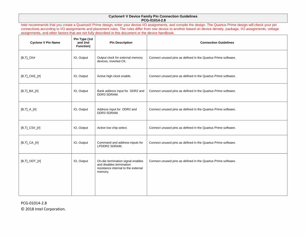
[B,T]_CK IO, Output Output clock for external memory devices.
Connect unused pins as defined in the Quartus Prime software.
Cyclone® V Device Family Pin Connection Guidelines PCG-01014-2.8
Intel recommends that you create a Quartus® Prime design, enter your device I/O assignments, and compile the design. The Quartus Prime design will check your pin connections according to I/O assignments and placement rules. The rules differ from one device to another based on device density, package, I/O assignments, voltage assignments, and other factors that are not fully described in this document or the device handbook.
PCG-01014-2.8 © 2018 Intel Corporation.
Cyclone V Pin Name Pin Type (1st
and 2nd Function)
Pin Description Connection Guidelines
[B,T]_CK# IO, Output Output clock for external memory devices, inverted CK.
Connect unused pins as defined in the Quartus Prime software.
[B,T]_CKE_[#] IO, Output Active high clock enable. Connect unused pins as defined in the Quartus Prime software.
[B,T]_BA_[#] IO, Output Bank address input for DDR2 and DDR3 SDRAM.
Connect unused pins as defined in the Quartus Prime software.
[B,T]_A_[#] IO, Output Address input for DDR2 and DDR3 SDRAM.
Connect unused pins as defined in the Quartus Prime software.
[B,T]_CS#_[#] IO, Output Active low chip select. Connect unused pins as defined in the Quartus Prime software.
[B,T]_CA_[#] IO, Output Command and address inputs for LPDDR2 SDRAM.
Connect unused pins as defined in the Quartus Prime software.
[B,T]_ODT_[#] IO, Output On-die termination signal enables and disables termination resistance internal to the external memory.
Connect unused pins as defined in the Quartus Prime software.
Cyclone® V Device Family Pin Connection Guidelines PCG-01014-2.8
Intel recommends that you create a Quartus® Prime design, enter your device I/O assignments, and compile the design. The Quartus Prime design will check your pin connections according to I/O assignments and placement rules. The rules differ from one device to another based on device density, package, I/O assignments, voltage assignments, and other factors that are not fully described in this document or the device handbook.
PCG-01014-2.8 © 2018 Intel Corporation.
Cyclone V Pin Name Pin Type (1st
and 2nd Function)
Pin Description Connection Guidelines
Reference Pins
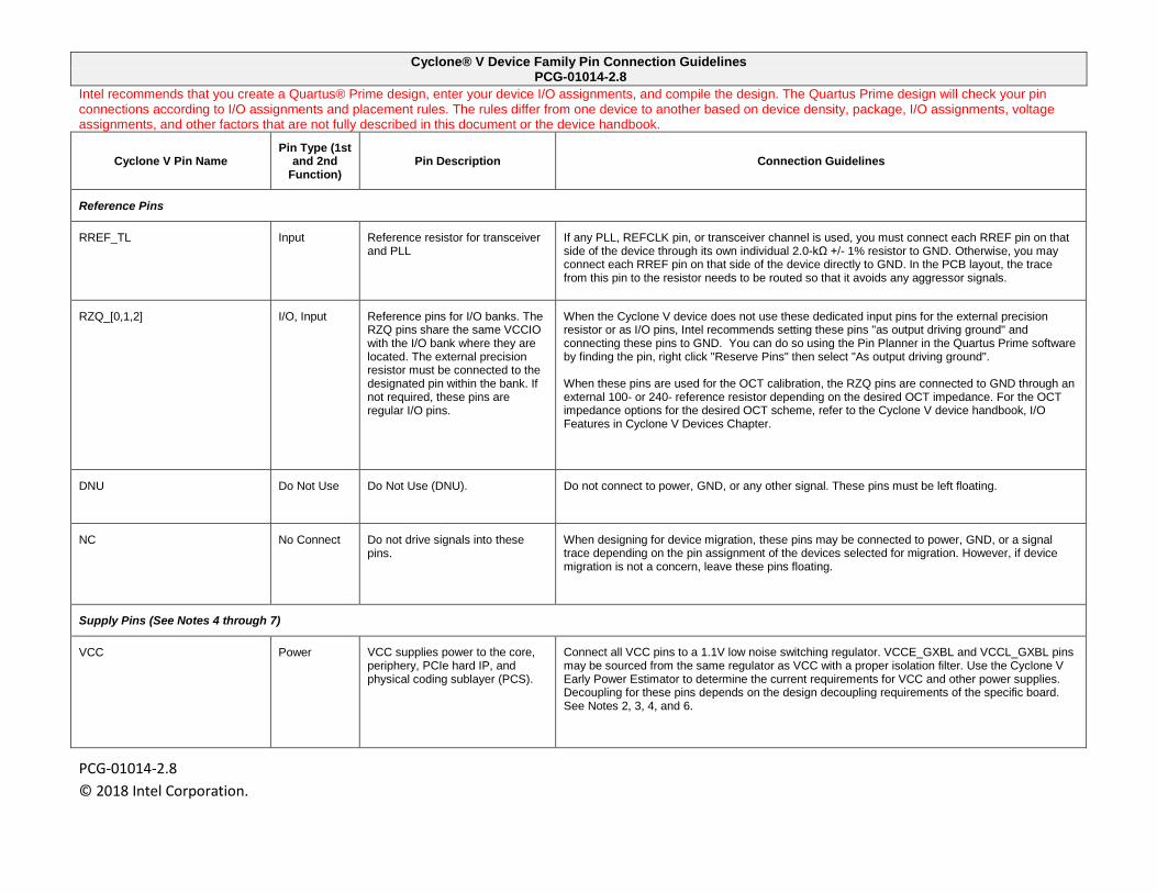
RREF_TL Input Reference resistor for transceiver and PLL
If any PLL, REFCLK pin, or transceiver channel is used, you must connect each RREF pin on that side of the device through its own individual 2.0-kΩ +/- 1% resistor to GND. Otherwise, you may connect each RREF pin on that side of the device directly to GND. In the PCB layout, the trace from this pin to the resistor needs to be routed so that it avoids any aggressor signals.
RZQ_[0,1,2] I/O, Input Reference pins for I/O banks. The RZQ pins share the same VCCIO with the I/O bank where they are located. The external precision resistor must be connected to the designated pin within the bank. If not required, these pins are regular I/O pins.
When the Cyclone V device does not use these dedicated input pins for the external precision resistor or as I/O pins, Intel recommends setting these pins "as output driving ground" and connecting these pins to GND. You can do so using the Pin Planner in the Quartus Prime software by finding the pin, right click "Reserve Pins" then select "As output driving ground". When these pins are used for the OCT calibration, the RZQ pins are connected to GND through an external 100- or 240- reference resistor depending on the desired OCT impedance. For the OCT impedance options for the desired OCT scheme, refer to the Cyclone V device handbook, I/O Features in Cyclone V Devices Chapter.
DNU Do Not Use Do Not Use (DNU). Do not connect to power, GND, or any other signal. These pins must be left floating.
NC No Connect Do not drive signals into these pins.
When designing for device migration, these pins may be connected to power, GND, or a signal trace depending on the pin assignment of the devices selected for migration. However, if device migration is not a concern, leave these pins floating.
Supply Pins (See Notes 4 through 7)
VCC Power VCC supplies power to the core, periphery, PCIe hard IP, and physical coding sublayer (PCS).
Connect all VCC pins to a 1.1V low noise switching regulator. VCCE_GXBL and VCCL_GXBL pins may be sourced from the same regulator as VCC with a proper isolation filter. Use the Cyclone V Early Power Estimator to determine the current requirements for VCC and other power supplies. Decoupling for these pins depends on the design decoupling requirements of the specific board. See Notes 2, 3, 4, and 6.
Cyclone® V Device Family Pin Connection Guidelines PCG-01014-2.8
Intel recommends that you create a Quartus® Prime design, enter your device I/O assignments, and compile the design. The Quartus Prime design will check your pin connections according to I/O assignments and placement rules. The rules differ from one device to another based on device density, package, I/O assignments, voltage assignments, and other factors that are not fully described in this document or the device handbook.
PCG-01014-2.8 © 2018 Intel Corporation.
Cyclone V Pin Name Pin Type (1st
and 2nd Function)
Pin Description Connection Guidelines
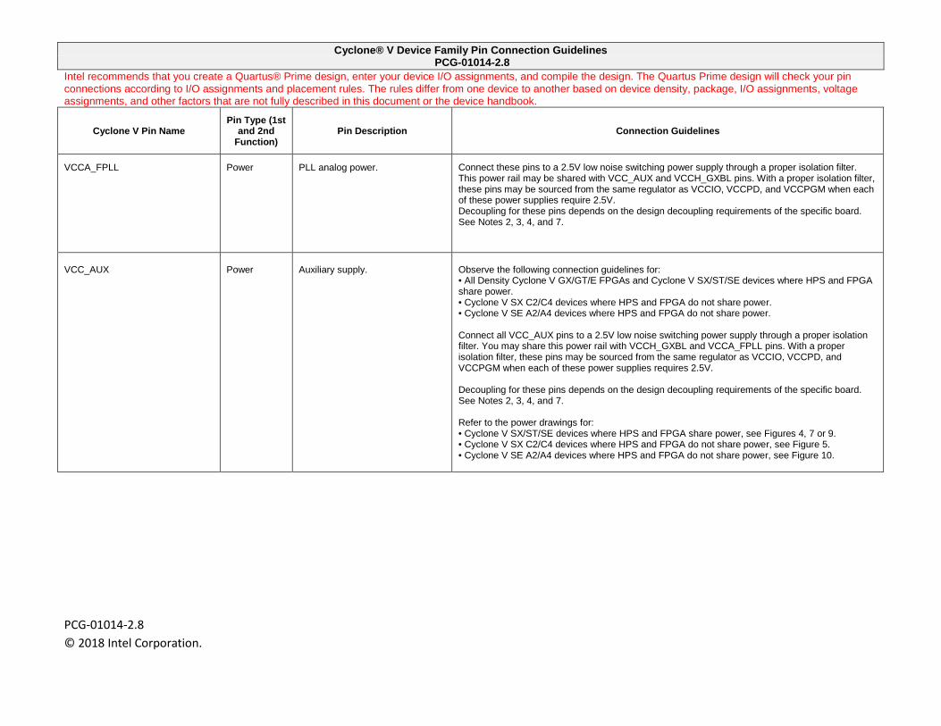
VCCA_FPLL Power PLL analog power. Connect these pins to a 2.5V low noise switching power supply through a proper isolation filter. This power rail may be shared with VCC_AUX and VCCH_GXBL pins. With a proper isolation filter, these pins may be sourced from the same regulator as VCCIO, VCCPD, and VCCPGM when each of these power supplies require 2.5V. Decoupling for these pins depends on the design decoupling requirements of the specific board. See Notes 2, 3, 4, and 7.
VCC_AUX
Power
Auxiliary supply.
Observe the following connection guidelines for: • All Density Cyclone V GX/GT/E FPGAs and Cyclone V SX/ST/SE devices where HPS and FPGA share power. • Cyclone V SX C2/C4 devices where HPS and FPGA do not share power. • Cyclone V SE A2/A4 devices where HPS and FPGA do not share power. Connect all VCC_AUX pins to a 2.5V low noise switching power supply through a proper isolation filter. You may share this power rail with VCCH_GXBL and VCCA_FPLL pins. With a proper isolation filter, these pins may be sourced from the same regulator as VCCIO, VCCPD, and VCCPGM when each of these power supplies requires 2.5V. Decoupling for these pins depends on the design decoupling requirements of the specific board. See Notes 2, 3, 4, and 7. Refer to the power drawings for: • Cyclone V SX/ST/SE devices where HPS and FPGA share power, see Figures 4, 7 or 9. • Cyclone V SX C2/C4 devices where HPS and FPGA do not share power, see Figure 5. • Cyclone V SE A2/A4 devices where HPS and FPGA do not share power, see Figure 10.
Cyclone® V Device Family Pin Connection Guidelines PCG-01014-2.8
Intel recommends that you create a Quartus® Prime design, enter your device I/O assignments, and compile the design. The Quartus Prime design will check your pin connections according to I/O assignments and placement rules. The rules differ from one device to another based on device density, package, I/O assignments, voltage assignments, and other factors that are not fully described in this document or the device handbook.
PCG-01014-2.8 © 2018 Intel Corporation.
Cyclone V Pin Name Pin Type (1st
and 2nd Function)
Pin Description Connection Guidelines
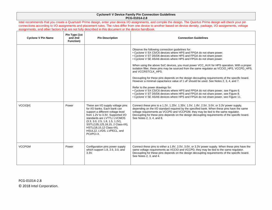
Observe the following connection guidelines for: • Cyclone V SX C5/C6 devices where HPS and FPGA do not share power. • Cyclone V ST D5/D6 devices where HPS and FPGA do not share power. • Cyclone V SE A5/A6 devices where HPS and FPGA do not share power. When using the above SoC devices, you must power VCC_AUX for HPS operation. With a proper isolation filter, these pins may be sourced from the same regulator as VCCIO_HPS, VCCPD_HPS, and VCCRSTCLK_HPS. Decoupling for these pins depends on the design decoupling requirements of the specific board. However a minimal capacitance value of 1 uF should be used. See Notes 2, 3, 4, and 7. Refer to the power drawings for: • Cyclone V SX C5/C6 devices where HPS and FPGA do not share power, see Figure 6. • Cyclone V ST D5/D6 devices where HPS and FPGA do not share power, see Figure 8. • Cyclone V SE A5/A6 devices where HPS and FPGA do not share power, see Figure 11.
VCCIO[#] Power These are I/O supply voltage pins for I/O banks. Each bank can support a different voltage level from 1.2V to 3.3V. Supported I/O standards are LVTTL/ LVCMOS (3.3, 3.0, 2.5, 1.8, 1.5, 1.2V), SSTL(135,125,18,15, 2 Class-I/II), HSTL(18,15,12 Class-I/II), HSUL12, LVDS, LVPECL, and PCI/PCI-X.
Connect these pins to a 1.2V, 1.25V, 1.35V, 1.5V, 1.8V, 2.5V, 3.0V, or 3.3V power supply, depending on the I/O standard required by the specified bank. When these pins have the same voltage requirements as VCCPD and VCCPGM, they may be tied to the same regulator. Decoupling for these pins depends on the design decoupling requirements of the specific board. See Notes 2, 3, 4, and 8.
VCCPGM Power Configuration pins power supply which support 1.8, 2.5, 3.0, and 3.3V.
Connect these pins to either a 1.8V, 2.5V, 3.0V, or 3.3V power supply. When these pins have the same voltage requirements as VCCIO and VCCPD, they may be tied to the same regulator. Decoupling for these pins depends on the design decoupling requirements of the specific board. See Notes 2, 3, and 4.
Cyclone® V Device Family Pin Connection Guidelines PCG-01014-2.8
Intel recommends that you create a Quartus® Prime design, enter your device I/O assignments, and compile the design. The Quartus Prime design will check your pin connections according to I/O assignments and placement rules. The rules differ from one device to another based on device density, package, I/O assignments, voltage assignments, and other factors that are not fully described in this document or the device handbook.
PCG-01014-2.8 © 2018 Intel Corporation.
Cyclone V Pin Name Pin Type (1st
and 2nd Function)
Pin Description Connection Guidelines
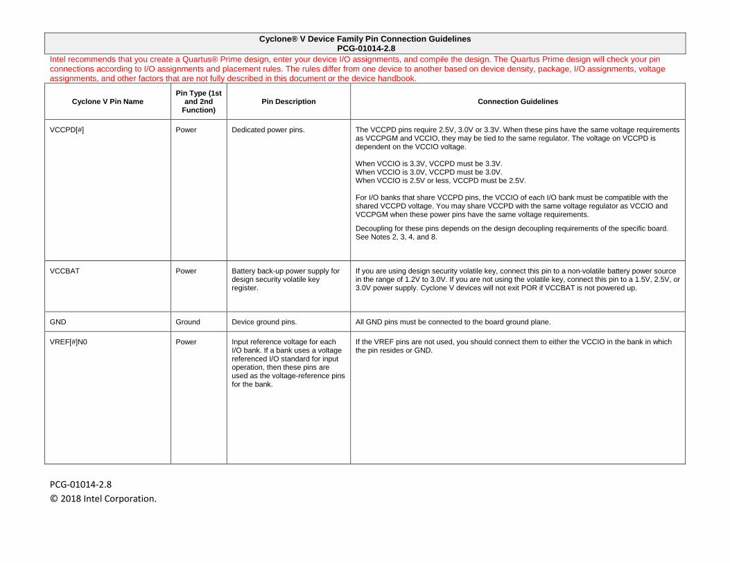
VCCPD[#] Power Dedicated power pins. The VCCPD pins require 2.5V, 3.0V or 3.3V. When these pins have the same voltage requirements as VCCPGM and VCCIO, they may be tied to the same regulator. The voltage on VCCPD is dependent on the VCCIO voltage. When VCCIO is 3.3V, VCCPD must be 3.3V. When VCCIO is 3.0V, VCCPD must be 3.0V. When VCCIO is 2.5V or less, VCCPD must be 2.5V. For I/O banks that share VCCPD pins, the VCCIO of each I/O bank must be compatible with the shared VCCPD voltage. You may share VCCPD with the same voltage regulator as VCCIO and VCCPGM when these power pins have the same voltage requirements.
Decoupling for these pins depends on the design decoupling requirements of the specific board. See Notes 2, 3, 4, and 8.
VCCBAT Power Battery back-up power supply for design security volatile key register.
If you are using design security volatile key, connect this pin to a non-volatile battery power source in the range of 1.2V to 3.0V. If you are not using the volatile key, connect this pin to a 1.5V, 2.5V, or 3.0V power supply. Cyclone V devices will not exit POR if VCCBAT is not powered up.
GND Ground Device ground pins. All GND pins must be connected to the board ground plane.
VREF[#]N0 Power Input reference voltage for each I/O bank. If a bank uses a voltage referenced I/O standard for input operation, then these pins are used as the voltage-reference pins for the bank.
If the VREF pins are not used, you should connect them to either the VCCIO in the bank in which the pin resides or GND.
Cyclone® V Device Family Pin Connection Guidelines PCG-01014-2.8
Intel recommends that you create a Quartus® Prime design, enter your device I/O assignments, and compile the design. The Quartus Prime design will check your pin connections according to I/O assignments and placement rules. The rules differ from one device to another based on device density, package, I/O assignments, voltage assignments, and other factors that are not fully described in this document or the device handbook.
PCG-01014-2.8 © 2018 Intel Corporation.
Cyclone V Pin Name Pin Type (1st
and 2nd Function)
Pin Description Connection Guidelines
Transceiver Pins (See Notes 4 through 10)
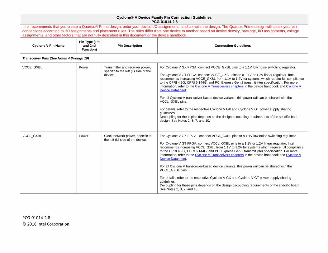
VCCE_GXBL Power Transmitter and receiver power, specific to the left (L) side of the device.
For Cyclone V GX FPGA, connect VCCE_GXBL pins to a 1.1V low noise switching regulator. For Cyclone V GT FPGA, connect VCCE_GXBL pins to a 1.1V or 1.2V linear regulator. Intel recommends increasing VCCE_GXBL from 1.1V to 1.2V for systems which require full compliance to the CPRI 4.9G, CPRI 6.144G, and PCI Express Gen 2 transmit jitter specification. For more information, refer to the Cyclone V Transceivers chapters in the device handbook and Cyclone V Device Datasheet. For all Cyclone V transceiver-based device variants, this power rail can be shared with the VCCL_GXBL pins. For details, refer to the respective Cyclone V GX and Cyclone V GT power supply sharing guidelines. Decoupling for these pins depends on the design decoupling requirements of the specific board design. See Notes 2, 3, 7, and 10.
VCCL_GXBL Power Clock network power, specific to the left (L) side of the device.
For Cyclone V GX FPGA , connect VCCL_GXBL pins to a 1.1V low noise switching regulator. For Cyclone V GT FPGA, connect VCCL_GXBL pins to a 1.1V or 1.2V linear regulator. Intel recommends increasing VCCL_GXBL from 1.1V to 1.2V for systems which require full compliance to the CPRI 4.9G, CPRI 6.144G, and PCI Express Gen 2 transmit jitter specification. For more information, refer to the Cyclone V Transceivers chapters in the device handbook and Cyclone V Device Datasheet. For all Cyclone V transceiver-based device variants, this power rail can be shared with the VCCE_GXBL pins. For details, refer to the respective Cyclone V GX and Cyclone V GT power supply sharing guidelines. Decoupling for these pins depends on the design decoupling requirements of the specific board. See Notes 2, 3, 7, and 10.
https://www.altera.com/content/dam/altera-www/global/en_US/pdfs/literature/hb/cyclone-v/cv_51002.pdf
https://www.altera.com/content/dam/altera-www/global/en_US/pdfs/literature/hb/cyclone-v/cv_51002.pdf
Cyclone® V Device Family Pin Connection Guidelines PCG-01014-2.8
Intel recommends that you create a Quartus® Prime design, enter your device I/O assignments, and compile the design. The Quartus Prime design will check your pin connections according to I/O assignments and placement rules. The rules differ from one device to another based on device density, package, I/O assignments, voltage assignments, and other factors that are not fully described in this document or the device handbook.
PCG-01014-2.8 © 2018 Intel Corporation.
Cyclone V Pin Name Pin Type (1st
and 2nd Function)
Pin Description Connection Guidelines
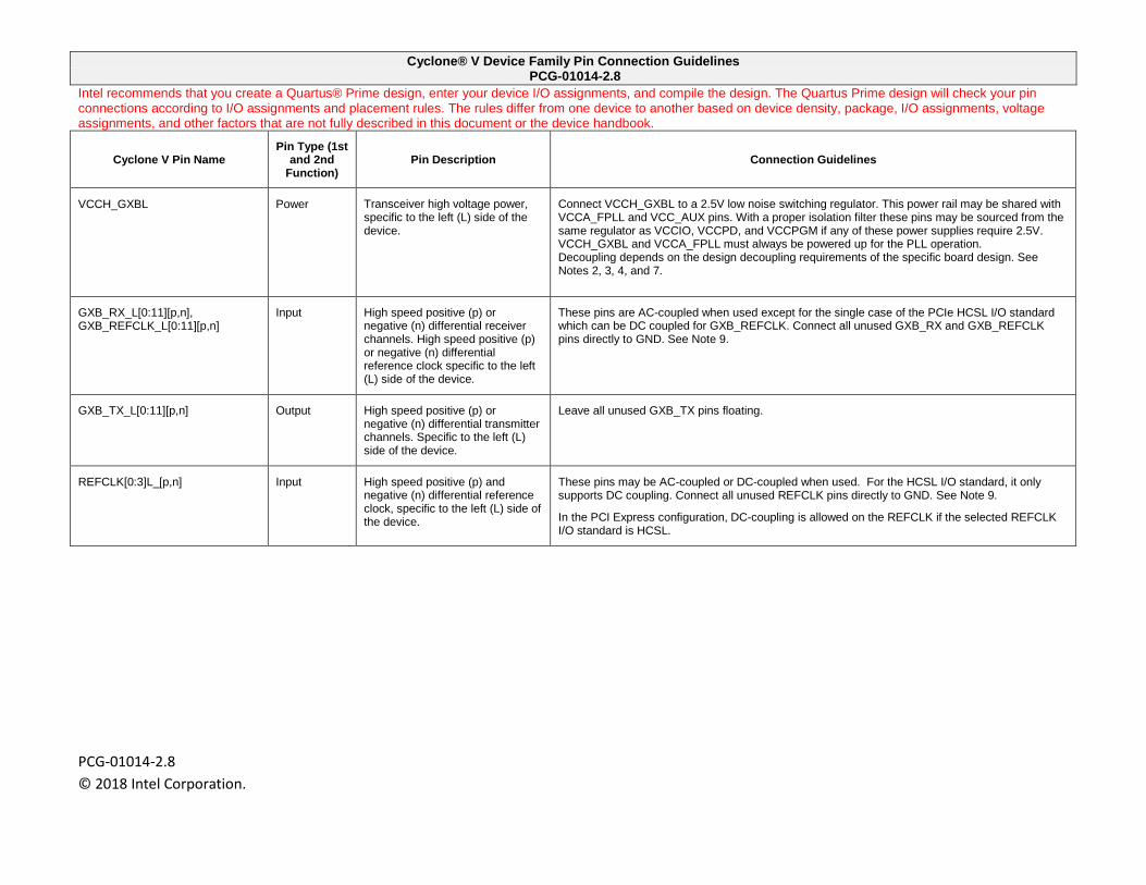
VCCH_GXBL Power Transceiver high voltage power, specific to the left (L) side of the device.
Connect VCCH_GXBL to a 2.5V low noise switching regulator. This power rail may be shared with VCCA_FPLL and VCC_AUX pins. With a proper isolation filter these pins may be sourced from the same regulator as VCCIO, VCCPD, and VCCPGM if any of these power supplies require 2.5V. VCCH_GXBL and VCCA_FPLL must always be powered up for the PLL operation. Decoupling depends on the design decoupling requirements of the specific board design. See Notes 2, 3, 4, and 7.
GXB_RX_L[0:11][p,n], GXB_REFCLK_L[0:11][p,n]
Input High speed positive (p) or negative (n) differential receiver channels. High speed positive (p) or negative (n) differential reference clock specific to the left (L) side of the device.
These pins are AC-coupled when used except for the single case of the PCIe HCSL I/O standard which can be DC coupled for GXB_REFCLK. Connect all unused GXB_RX and GXB_REFCLK pins directly to GND. See Note 9.
GXB_TX_L[0:11][p,n] Output High speed positive (p) or negative (n) differential transmitter channels. Specific to the left (L) side of the device.
Leave all unused GXB_TX pins floating.
REFCLK[0:3]L_[p,n] Input High speed positive (p) and negative (n) differential reference clock, specific to the left (L) side of the device.
These pins may be AC-coupled or DC-coupled when used. For the HCSL I/O standard, it only supports DC coupling. Connect all unused REFCLK pins directly to GND. See Note 9.
In the PCI Express configuration, DC-coupling is allowed on the REFCLK if the selected REFCLK I/O standard is HCSL.
Cyclone® V Device Family Pin Connection Guidelines PCG-01014-2.8
Intel recommends that you create a Quartus® Prime design, enter your device I/O assignments, and compile the design. The Quartus Prime design will check your pin connections according to I/O assignments and placement rules. The rules differ from one device to another based on device density, package, I/O assignments, voltage assignments, and other factors that are not fully described in this document or the device handbook.
PCG-01014-2.8 © 2018 Intel Corporation.
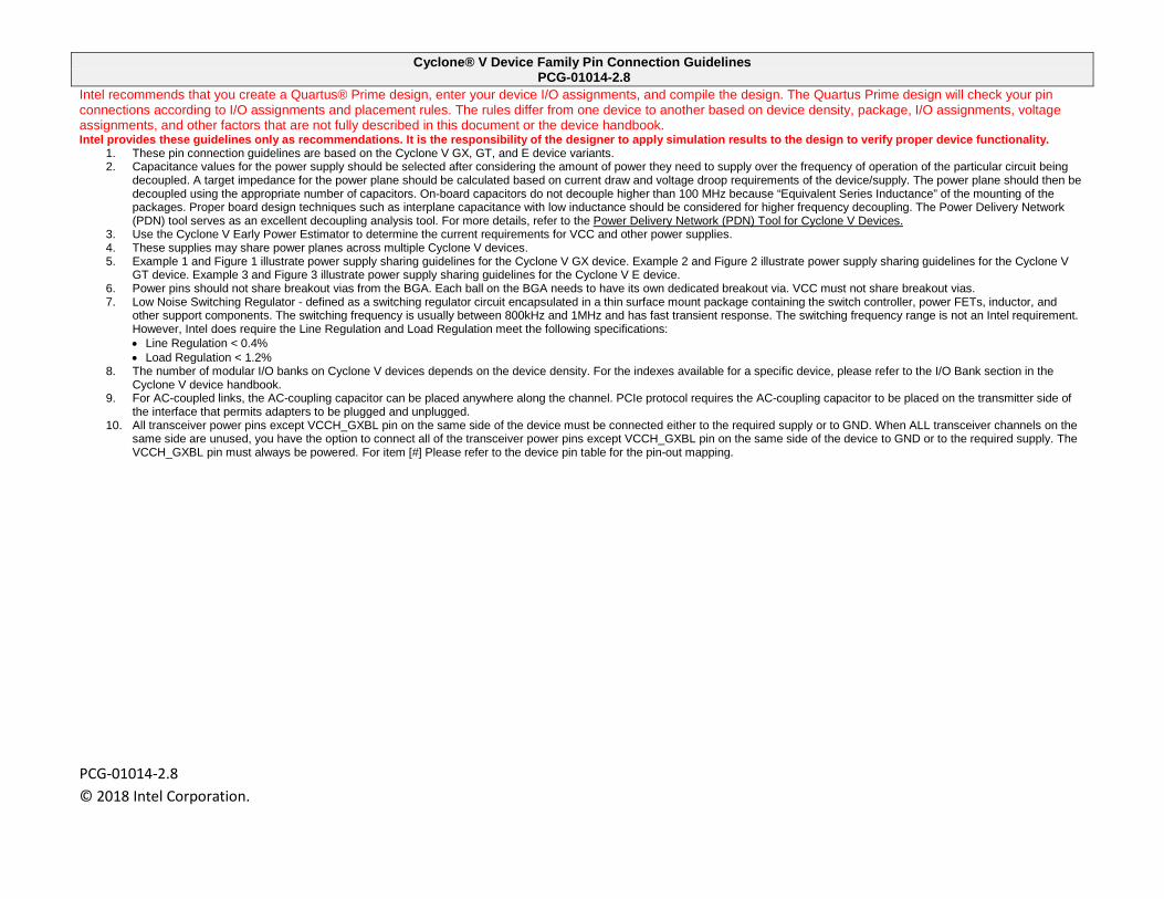
Intel provides these guidelines only as recommendations. It is the responsibility of the designer to apply simulation results to the design to verify proper device functionality. 1. These pin connection guidelines are based on the Cyclone V GX, GT, and E device variants. 2. Capacitance values for the power supply should be selected after considering the amount of power they need to supply over the frequency of operation of the particular circuit being
decoupled. A target impedance for the power plane should be calculated based on current draw and voltage droop requirements of the device/supply. The power plane should then be decoupled using the appropriate number of capacitors. On-board capacitors do not decouple higher than 100 MHz because “Equivalent Series Inductance” of the mounting of the packages. Proper board design techniques such as interplane capacitance with low inductance should be considered for higher frequency decoupling. The Power Delivery Network (PDN) tool serves as an excellent decoupling analysis tool. For more details, refer to the Power Delivery Network (PDN) Tool for Cyclone V Devices.
3. Use the Cyclone V Early Power Estimator to determine the current requirements for VCC and other power supplies. 4. These supplies may share power planes across multiple Cyclone V devices. 5. Example 1 and Figure 1 illustrate power supply sharing guidelines for the Cyclone V GX device. Example 2 and Figure 2 illustrate power supply sharing guidelines for the Cyclone V
GT device. Example 3 and Figure 3 illustrate power supply sharing guidelines for the Cyclone V E device. 6. Power pins should not share breakout vias from the BGA. Each ball on the BGA needs to have its own dedicated breakout via. VCC must not share breakout vias. 7. Low Noise Switching Regulator - defined as a switching regulator circuit encapsulated in a thin surface mount package containing the switch controller, power FETs, inductor, and
other support components. The switching frequency is usually between 800kHz and 1MHz and has fast transient response. The switching frequency range is not an Intel requirement. However, Intel does require the Line Regulation and Load Regulation meet the following specifications: • Line Regulation < 0.4% • Load Regulation < 1.2%
8. The number of modular I/O banks on Cyclone V devices depends on the device density. For the indexes available for a specific device, please refer to the I/O Bank section in the Cyclone V device handbook.
9. For AC-coupled links, the AC-coupling capacitor can be placed anywhere along the channel. PCIe protocol requires the AC-coupling capacitor to be placed on the transmitter side of the interface that permits adapters to be plugged and unplugged.
10. All transceiver power pins except VCCH_GXBL pin on the same side of the device must be connected either to the required supply or to GND. When ALL transceiver channels on the same side are unused, you have the option to connect all of the transceiver power pins except VCCH_GXBL pin on the same side of the device to GND or to the required supply. The VCCH_GXBL pin must always be powered. For item [#] Please refer to the device pin table for the pin-out mapping.
Cyclone® V Device Family Pin Connection Guidelines PCG-01014-2.8
Intel recommends that you create a Quartus® Prime design, enter your device I/O assignments, and compile the design. The Quartus Prime design will check your pin connections according to I/O assignments and placement rules. The rules differ from one device to another based on device density, package, I/O assignments, voltage assignments, and other factors that are not fully described in this document or the device handbook.
PCG-01014-2.8 © 2018 Intel Corporation.
HPS Pin Connection Guidelines
Cyclone V HPS Pin Name
Pin Type (1st and
2nd Function)
Pin Description Connection Guidelines
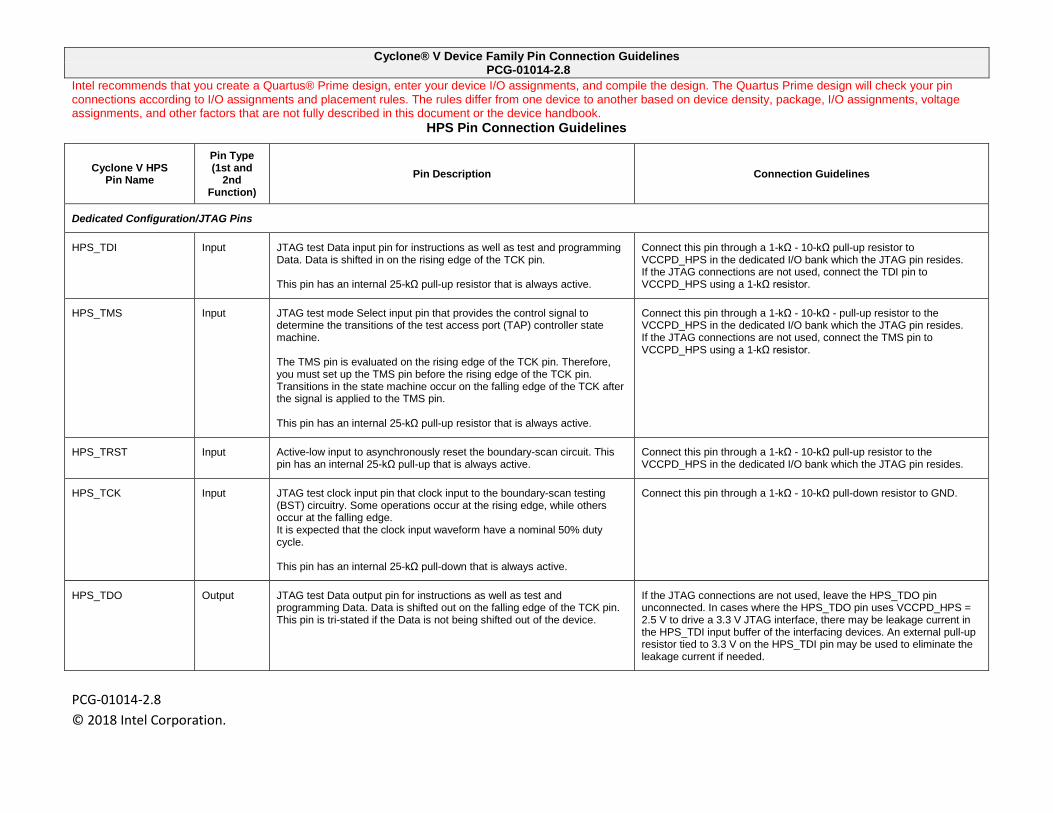
Dedicated Configuration/JTAG Pins
HPS_TDI Input JTAG test Data input pin for instructions as well as test and programming Data. Data is shifted in on the rising edge of the TCK pin. This pin has an internal 25-kΩ pull-up resistor that is always active.
Connect this pin through a 1-kΩ - 10-kΩ pull-up resistor to VCCPD_HPS in the dedicated I/O bank which the JTAG pin resides. If the JTAG connections are not used, connect the TDI pin to VCCPD_HPS using a 1-kΩ resistor.
HPS_TMS Input JTAG test mode Select input pin that provides the control signal to determine the transitions of the test access port (TAP) controller state machine. The TMS pin is evaluated on the rising edge of the TCK pin. Therefore, you must set up the TMS pin before the rising edge of the TCK pin. Transitions in the state machine occur on the falling edge of the TCK after the signal is applied to the TMS pin. This pin has an internal 25-kΩ pull-up resistor that is always active.
Connect this pin through a 1-kΩ - 10-kΩ - pull-up resistor to the VCCPD_HPS in the dedicated I/O bank which the JTAG pin resides. If the JTAG connections are not used, connect the TMS pin to VCCPD_HPS using a 1-kΩ resistor.
HPS_TRST Input Active-low input to asynchronously reset the boundary-scan circuit. This pin has an internal 25-kΩ pull-up that is always active.
Connect this pin through a 1-kΩ - 10-kΩ pull-up resistor to the VCCPD_HPS in the dedicated I/O bank which the JTAG pin resides.
HPS_TCK Input JTAG test clock input pin that clock input to the boundary-scan testing (BST) circuitry. Some operations occur at the rising edge, while others occur at the falling edge. It is expected that the clock input waveform have a nominal 50% duty cycle. This pin has an internal 25-kΩ pull-down that is always active.
Connect this pin through a 1-kΩ - 10-kΩ pull-down resistor to GND.
HPS_TDO Output JTAG test Data output pin for instructions as well as test and programming Data. Data is shifted out on the falling edge of the TCK pin. This pin is tri-stated if the Data is not being shifted out of the device.
If the JTAG connections are not used, leave the HPS_TDO pin unconnected. In cases where the HPS_TDO pin uses VCCPD_HPS = 2.5 V to drive a 3.3 V JTAG interface, there may be leakage current in the HPS_TDI input buffer of the interfacing devices. An external pull-up resistor tied to 3.3 V on the HPS_TDI pin may be used to eliminate the leakage current if needed.
Cyclone® V Device Family Pin Connection Guidelines PCG-01014-2.8
Intel recommends that you create a Quartus® Prime design, enter your device I/O assignments, and compile the design. The Quartus Prime design will check your pin connections according to I/O assignments and placement rules. The rules differ from one device to another based on device density, package, I/O assignments, voltage assignments, and other factors that are not fully described in this document or the device handbook.
PCG-01014-2.8 © 2018 Intel Corporation.
Cyclone V HPS Pin Name
Pin Type (1st and
2nd Function)
Pin Description Connection Guidelines
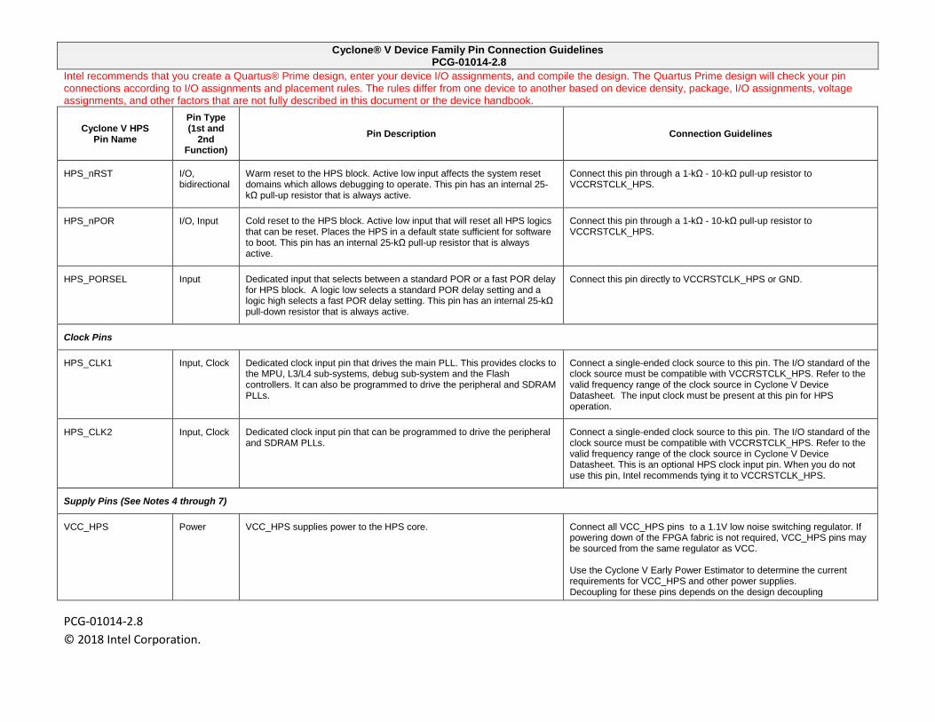
HPS_nRST I/O, bidirectional
Warm reset to the HPS block. Active low input affects the system reset domains which allows debugging to operate. This pin has an internal 25-kΩ pull-up resistor that is always active.
Connect this pin through a 1-kΩ - 10-kΩ pull-up resistor to VCCRSTCLK_HPS.
HPS_nPOR I/O, Input Cold reset to the HPS block. Active low input that will reset all HPS logics that can be reset. Places the HPS in a default state sufficient for software to boot. This pin has an internal 25-kΩ pull-up resistor that is always active.
Connect this pin through a 1-kΩ - 10-kΩ pull-up resistor to VCCRSTCLK_HPS.
HPS_PORSEL Input Dedicated input that selects between a standard POR or a fast POR delay for HPS block. A logic low selects a standard POR delay setting and a logic high selects a fast POR delay setting. This pin has an internal 25-kΩ pull-down resistor that is always active.
Connect this pin directly to VCCRSTCLK_HPS or GND.
Clock Pins
HPS_CLK1 Input, Clock Dedicated clock input pin that drives the main PLL. This provides clocks to the MPU, L3/L4 sub-systems, debug sub-system and the Flash controllers. It can also be programmed to drive the peripheral and SDRAM PLLs.
Connect a single-ended clock source to this pin. The I/O standard of the clock source must be compatible with VCCRSTCLK_HPS. Refer to the valid frequency range of the clock source in Cyclone V Device Datasheet. The input clock must be present at this pin for HPS operation.
HPS_CLK2 Input, Clock Dedicated clock input pin that can be programmed to drive the peripheral and SDRAM PLLs.
Connect a single-ended clock source to this pin. The I/O standard of the clock source must be compatible with VCCRSTCLK_HPS. Refer to the valid frequency range of the clock source in Cyclone V Device Datasheet. This is an optional HPS clock input pin. When you do not use this pin, Intel recommends tying it to VCCRSTCLK_HPS.
Supply Pins (See Notes 4 through 7)
VCC_HPS Power VCC_HPS supplies power to the HPS core. Connect all VCC_HPS pins to a 1.1V low noise switching regulator. If powering down of the FPGA fabric is not required, VCC_HPS pins may be sourced from the same regulator as VCC. Use the Cyclone V Early Power Estimator to determine the current requirements for VCC_HPS and other power supplies. Decoupling for these pins depends on the design decoupling
Cyclone® V Device Family Pin Connection Guidelines PCG-01014-2.8
Intel recommends that you create a Quartus® Prime design, enter your device I/O assignments, and compile the design. The Quartus Prime design will check your pin connections according to I/O assignments and placement rules. The rules differ from one device to another based on device density, package, I/O assignments, voltage assignments, and other factors that are not fully described in this document or the device handbook.
PCG-01014-2.8 © 2018 Intel Corporation.
Cyclone V HPS Pin Name
Pin Type (1st and
2nd Function)
Pin Description Connection Guidelines
requirements of the specific board. See Notes 2, 3, 4, and 6.
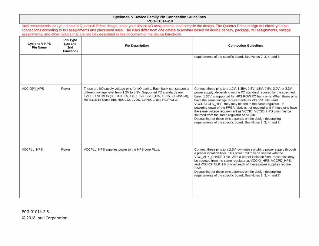
VCCIO[#]_HPS Power These are I/O supply voltage pins for I/O banks. Each bank can support a different voltage level from 1.2V to 3.3V. Supported I/O standards are LVTTL/ LVCMOS (3.3, 3.0, 2.5, 1.8, 1.5V), SSTL(135, 18,15, 2 Class-I/II), HSTL(18,15 Class-I/II), HSUL12, LVDS, LVPECL, and PCI/PCI-X.
Connect these pins to a 1.2V, 1.35V, 1.5V, 1.8V, 2.5V, 3.0V, or 3.3V power supply, depending on the I/O standard required by the specified bank. 1.35V is supported for HPS ROW I/O bank only. When these pins have the same voltage requirements as VCCPD_HPS and VCCRSTCLK_HPS, they may be tied to the same regulator. If powering down of the FPGA fabric is not required and if these pins have the same voltage requirement as VCCIO, VCCIO_HPS pins may be sourced from the same regulator as VCCIO. Decoupling for these pins depends on the design decoupling requirements of the specific board. See Notes 2, 3, 4, and 8.
VCCPLL_HPS Power VCCPLL_HPS supplies power to the HPS core PLLs. Connect these pins to a 2.5V low noise switching power supply through a proper isolation filter. This power rail may be shared with the VCC_AUX_SHARED pin. With a proper isolation filter, these pins may be sourced from the same regulator as VCCIO_HPS, VCCPD_HPS, and VCCRSTCLK_HPS when each of these power supplies require 2.5V. Decoupling for these pins depends on the design decoupling requirements of the specific board. See Notes 2, 3, 4, and 7.
Cyclone® V Device Family Pin Connection Guidelines PCG-01014-2.8
Intel recommends that you create a Quartus® Prime design, enter your device I/O assignments, and compile the design. The Quartus Prime design will check your pin connections according to I/O assignments and placement rules. The rules differ from one device to another based on device density, package, I/O assignments, voltage assignments, and other factors that are not fully described in this document or the device handbook.
PCG-01014-2.8 © 2018 Intel Corporation.
Cyclone V HPS Pin Name
Pin Type (1st and
2nd Function)
Pin Description Connection Guidelines
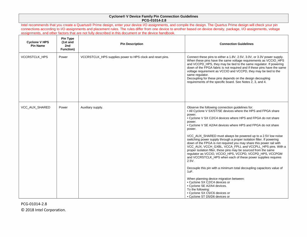
VCCRSTCLK_HPS Power VCCRSTCLK_HPS supplies power to HPS clock and reset pins. Connect these pins to either a 1.8V, 2.5V, 3.0V, or 3.3V power supply. When these pins have the same voltage requirements as VCCIO_HPS and VCCPD_HPS, they may be tied to the same regulator. If powering down of the FPGA fabric is not required and if these pins have the same voltage requirement as VCCIO and VCCPD, they may be tied to the same regulator. Decoupling for these pins depends on the design decoupling requirements of the specific board. See Notes 2, 3, and 4.
VCC_AUX_SHARED
Power
Auxiliary supply.
Observe the following connection guidelines for: • All Cyclone V SX/ST/SE devices where the HPS and FPGA share power. • Cyclone V SX C2/C4 devices where HPS and FPGA do not share power. • Cyclone V SE A2/A4 devices where HPS and FPGA do not share power. VCC_AUX_SHARED must always be powered up to a 2.5V low noise switching power supply through a proper isolation filter. If powering down of the FPGA is not required you may share this power rail with VCC_AUX, VCCH_GXBL, VCCA_FPLL and VCCPLL_HPS pins. With a proper isolation filter, these pins may be sourced from the same regulator as VCCIO, VCCIO_HPS, VCCPD, VCCPD_HPS, VCCPGM and VCCRSTCLK_HPS when each of these power supplies requires 2.5V. Decouple this pin with a minimum total decoupling capacitors value of 1uF. When planning device migration between: • Cyclone SX C2/C4 devices or • Cyclone SE A2/A4 devices. To the following: • Cyclone SX C5/C6 devices or • Cyclone ST D5/D6 devices or
Cyclone® V Device Family Pin Connection Guidelines PCG-01014-2.8
Intel recommends that you create a Quartus® Prime design, enter your device I/O assignments, and compile the design. The Quartus Prime design will check your pin connections according to I/O assignments and placement rules. The rules differ from one device to another based on device density, package, I/O assignments, voltage assignments, and other factors that are not fully described in this document or the device handbook.
PCG-01014-2.8 © 2018 Intel Corporation.
Cyclone V HPS Pin Name
Pin Type (1st and
2nd Function)
Pin Description Connection Guidelines
• Cyclone SE A5/A6 devices. You must follow the power supply sharing guidelines for: • Cyclone SX C5/C6 devices or • Cyclone ST D5/D6 devices or • Cyclone SE A5/A6 devices. See Notes 2, 3, 4, and 7. Refer to the power drawings for: • Cyclone V SX/ST/SE devices where HPS and FPGA share power, see Figures 4, 7 or 9. • Cyclone V SX C2/C4 devices where HPS and FPGA do not share power, see Figure 5. • Cyclone V SE A2/A4 devices where HPS and FPGA do not share power, see Figure 10. Observe the following connection guidelines for: • Cyclone V SX C5/C6 devices where HPS and FPGA do not share power. • Cyclone V ST D5/D6 devices where HPS and FPGA do not share power. • Cyclone V SE A5/A6 devices where HPS and FPGA do not share power. If powering down the FPGA fabric is required, connect this pin through a separate isolation filter to 2.5V. The filter consists of an EMI Suppression Ferrite Bead along with a minimum decoupling capacitors value of 1 uF. The ferrite bead should have an impedance of not less than 30 ohms at 100 MHz and a max impedance of 65 ohms at 1000 MHz. The bead is connected to 2.5V at one end and the other end is connected to the VCC_AUX_SHARED pin. The capacitor should connect between the VCC_AUX_SHARED pin and ground. Both components should be placed close to the VCC_AUX_SHARED pin. Refer to AN583: Designing Power Isolation Filters with Ferrite Beads for Intel FPGAs for further guidance. With this filter you may source VCC_AUX_SHARED from the same regulator as VCCIO_HPS, VCCPD_HPS and VCCRSTCLK_HPS.
Cyclone® V Device Family Pin Connection Guidelines PCG-01014-2.8
Intel recommends that you create a Quartus® Prime design, enter your device I/O assignments, and compile the design. The Quartus Prime design will check your pin connections according to I/O assignments and placement rules. The rules differ from one device to another based on device density, package, I/O assignments, voltage assignments, and other factors that are not fully described in this document or the device handbook.
PCG-01014-2.8 © 2018 Intel Corporation.
Cyclone V HPS Pin Name
Pin Type (1st and
2nd Function)
Pin Description Connection Guidelines
See Notes 2, 3, 4, and 7. Refer to the power drawings for: • Cyclone V SX C5/C6 devices where HPS and FPGA do not share power, see Figure 6. • Cyclone V ST D5/D6 devices where HPS and FPGA do not share power, see Figure 8. • Cyclone V SE A5/A6 devices where HPS and FPGA do not share power, see Figure 11.
VCCPD[#]_HPS Power Dedicated power pins. The VCCPD_HPS pins require 2.5V, 3.0V or 3.3V. When these pins have the same voltage requirements as VCCRSTCLK_HPS and VCCIO_HPS, they may be tied to the same regulator. The voltage on VCCPD_HPS is dependent on the VCCIO_HPS voltage. If powering down of the FPGA fabric is not required and if these pins have the same voltage requirement as VCCPD, they may be tied to the same regulator.When VCCIO_HPS is 3.3V, VCCPD_HPS must be 3.3V.When VCCIO_HPS is 3.0V, VCCPD_HPS must be 3.0V.When VCCIO_HPS is 2.5V or less, VCCPD_HPS must be 2.5V.Decoupling for these pins depends on the design decoupling requirements of the specific board. See Notes 2, 3, 4, and 8.
VREFB[#]N0_HPS I/O, Power Input reference voltage for each I/O bank. If a bank uses a voltage referenced I/O standard for input operation, then these pins are used as the voltage-reference pins for the bank.
VREF pins will source current and the regulator used for VREF pins should have the capability to sink and source current.
If the VREF pins are not used, you should connect them to either the VCCIO in the bank in which the pin resides or GND.
Hard Memory PHY Pins
HPS_DQ[#] I/O, bidirectional
Optional data signal for use in external memory interfacing. Use caution when making pin assignments if you plan on migrating to a different memory interface that has a different HPS_DQ bus width. Analyze the available HPS_DQ pins across all pertinent HPS_DQS columns in the pin list.
If hard memory PHY is used, connection to memory device DQ pin must start from [B,T]_DQ_0 pin. For details, refer to the specific device pinout file. Connect unused pins as defined in the Quartus Prime software.
Cyclone® V Device Family Pin Connection Guidelines PCG-01014-2.8
Intel recommends that you create a Quartus® Prime design, enter your device I/O assignments, and compile the design. The Quartus Prime design will check your pin connections according to I/O assignments and placement rules. The rules differ from one device to another based on device density, package, I/O assignments, voltage assignments, and other factors that are not fully described in this document or the device handbook.
PCG-01014-2.8 © 2018 Intel Corporation.
Cyclone V HPS Pin Name
Pin Type (1st and
2nd Function)
Pin Description Connection Guidelines
HPS_DQS_[#] I/O, bidirectional
Optional data strobe signal for use in external memory interfacing. These pins drive to dedicated HPS_DQS phase shift circuitry. The shifted DQS signal can also drive to internal logic.
If hard memory PHY is used, connection to memory device DQS pin must start from [B,T]_DQS_0 pin. For details, refer to the specific device pinout file. Connect unused pins as defined in the Quartus Prime software.
HPS_DQS#_[#] I/O, bidirectional
Optional complementary data strobe signal for use in external memory interfacing. These pins drive to dedicated HPS_DQS phase shift circuitry.
If hard memory PHY is used, connection to memory device DQSn pin must start from [B,T]_DQS#_0 pin. For details, refer to the specific device pinout file. Connect unused pins as defined in the Quartus Prime software.
HPS_DM_[#] I/O, Output Optional write data mask, edge-aligned to HPS_DQ during write. Connect unused pins as defined in the Quartus Prime software.
HPS_WE# I/O, Output Write-Enable input for DDR2 andDDR3 SDRAM. Connect unused pins as defined in the Quartus Prime software.
HPS_CAS# I/O, Output Column address strobe for DDR2 and DDR3 SDRAM. Connect unused pins as defined in the Quartus Prime software.
HPS_RAS# I/O, Output Row address strobe for DDR2 and DDR3 SDRAM. Connect unused pins as defined in the Quartus Prime software.
HPS_RESET# I/O, Output Active low reset signal. Connect unused pins as defined in the Quartus Prime software.
HPS_CK I/O, Output Output clock for external memory devices. Connect unused pins as defined in the Quartus Prime software.
HPS_CK# I/O, Output Output clock for external memory devices, inverted CK. Connect unused pins as defined in the Quartus Prime software.
Cyclone® V Device Family Pin Connection Guidelines PCG-01014-2.8
Intel recommends that you create a Quartus® Prime design, enter your device I/O assignments, and compile the design. The Quartus Prime design will check your pin connections according to I/O assignments and placement rules. The rules differ from one device to another based on device density, package, I/O assignments, voltage assignments, and other factors that are not fully described in this document or the device handbook.
PCG-01014-2.8 © 2018 Intel Corporation.
Cyclone V HPS Pin Name
Pin Type (1st and
2nd Function)
Pin Description Connection Guidelines
HPS_CKE_[#] I/O, Output Active high clock Enable. Connect unused pins as defined in the Quartus Prime software.
HPS_BA_[#] I/O, Output Bank address input for DDR2 and DDR3 SDRAM. Connect unused pins as defined in the Quartus Prime software.
HPS_A_[#] I/O, Output Address input for DDR2 and DDR3 SDRAM. Connect unused pins as defined in the Quartus Prime software.
HPS_CA_[#] I/O, Output Command and address inputs for LPDDR and LPDDR2 SDRAM. Connect unused pins as defined in the Quartus Prime software.
HPS_CS#_[#] I/O, Output Active low chip Select. Connect unused pins as defined in the Quartus Prime software.
HPS_ODT_[#] I/O, Output On-die termination signal enables and disables termination resistance internal to the external memory.
Connect unused pins as defined in the Quartus Prime software.
Reference Pins
HPS_RZQ_0 I/O, Input Reference pins for I/O banks. The HPS_RZQ_0 pins shares the same HPS_VCCIO with the I/O bank where it is located. The external precision resistor must be connected to the designated pin within the bank. If not required, these pins are regular I/O pins.
When the Cyclone V SoC device does not use these dedicated input pins for the external precision resistor or as I/O pins, Intel recommends connecting these pins to GND. When these pins are used for the OCT calibration, the HPS_RZQ_0 pin is connected to GND through an external 100-Ω or 240-Ω reference resistor depending on the desired OCT impedance. For the OCT impedance options for the desired OCT scheme, refer to the Cyclone V device handbook, I/O Features in Cyclone V Devices Chapter.
General Purpose Input Pins (See Note 13)
HPS_GPI# Input General purpose inputs signals in the SDRAM bank These pins use the same VCCIO_HPS as the other HPS SDRAM pins. If unused, program them in Quartus as an input with a weak pull-up.
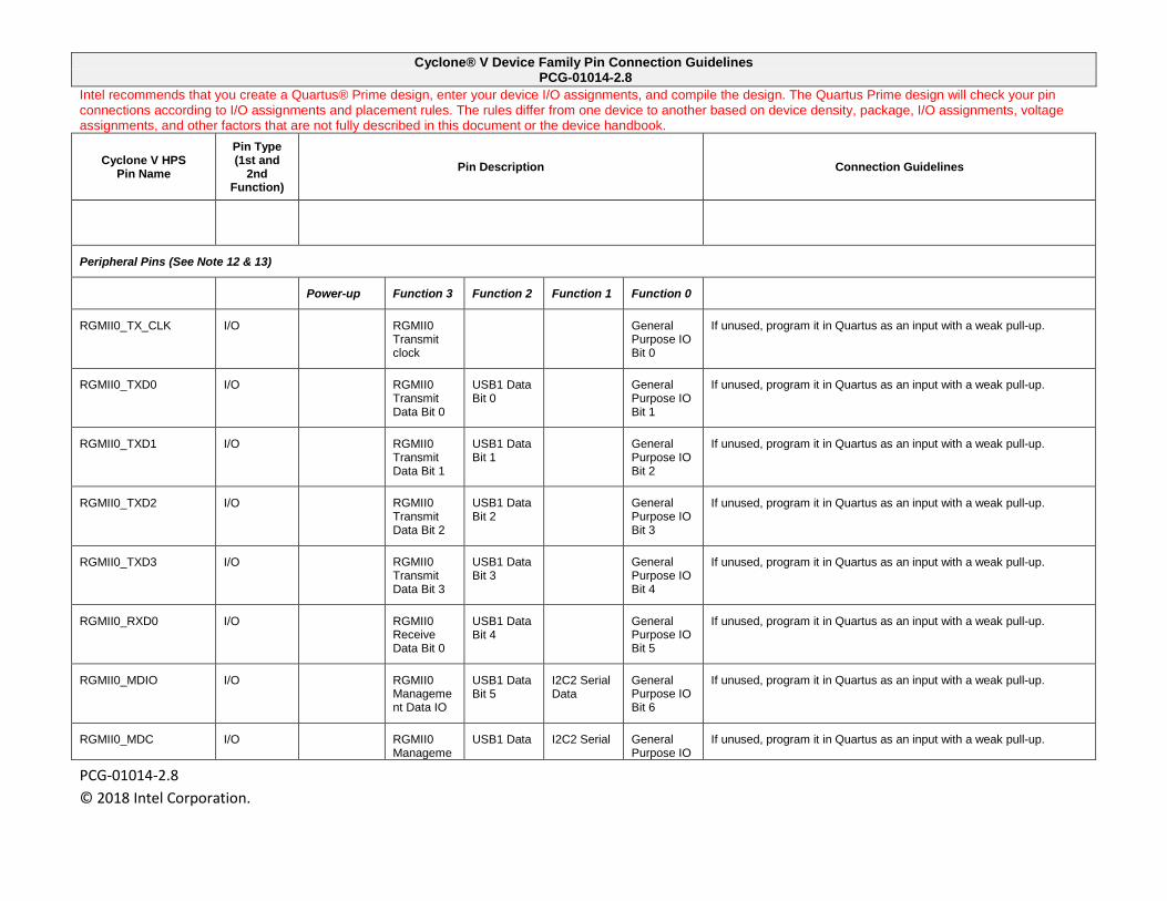
Cyclone® V Device Family Pin Connection Guidelines PCG-01014-2.8
Intel recommends that you create a Quartus® Prime design, enter your device I/O assignments, and compile the design. The Quartus Prime design will check your pin connections according to I/O assignments and placement rules. The rules differ from one device to another based on device density, package, I/O assignments, voltage assignments, and other factors that are not fully described in this document or the device handbook.
PCG-01014-2.8 © 2018 Intel Corporation.
Cyclone V HPS Pin Name
Pin Type (1st and
2nd Function)
Pin Description Connection Guidelines
Peripheral Pins (See Note 12 & 13)
Power-up Function 3 Function 2 Function 1 Function 0
RGMII0_TX_CLK I/O RGMII0 Transmit clock
General Purpose IO Bit 0
If unused, program it in Quartus as an input with a weak pull-up.
RGMII0_TXD0 I/O RGMII0 Transmit Data Bit 0
USB1 Data Bit 0
General Purpose IO Bit 1
If unused, program it in Quartus as an input with a weak pull-up.
RGMII0_TXD1 I/O RGMII0 Transmit Data Bit 1
USB1 Data Bit 1
General Purpose IO Bit 2
If unused, program it in Quartus as an input with a weak pull-up.
RGMII0_TXD2 I/O RGMII0 Transmit Data Bit 2
USB1 Data Bit 2
General Purpose IO Bit 3
If unused, program it in Quartus as an input with a weak pull-up.
RGMII0_TXD3 I/O RGMII0 Transmit Data Bit 3
USB1 Data Bit 3
General Purpose IO Bit 4
If unused, program it in Quartus as an input with a weak pull-up.
RGMII0_RXD0 I/O RGMII0 Receive Data Bit 0
USB1 Data Bit 4
General Purpose IO Bit 5
If unused, program it in Quartus as an input with a weak pull-up.
RGMII0_MDIO I/O RGMII0 Management Data IO
USB1 Data Bit 5
I2C2 Serial Data
General Purpose IO Bit 6
If unused, program it in Quartus as an input with a weak pull-up.
RGMII0_MDC I/O RGMII0 Manageme
USB1 Data I2C2 Serial General Purpose IO
If unused, program it in Quartus as an input with a weak pull-up.
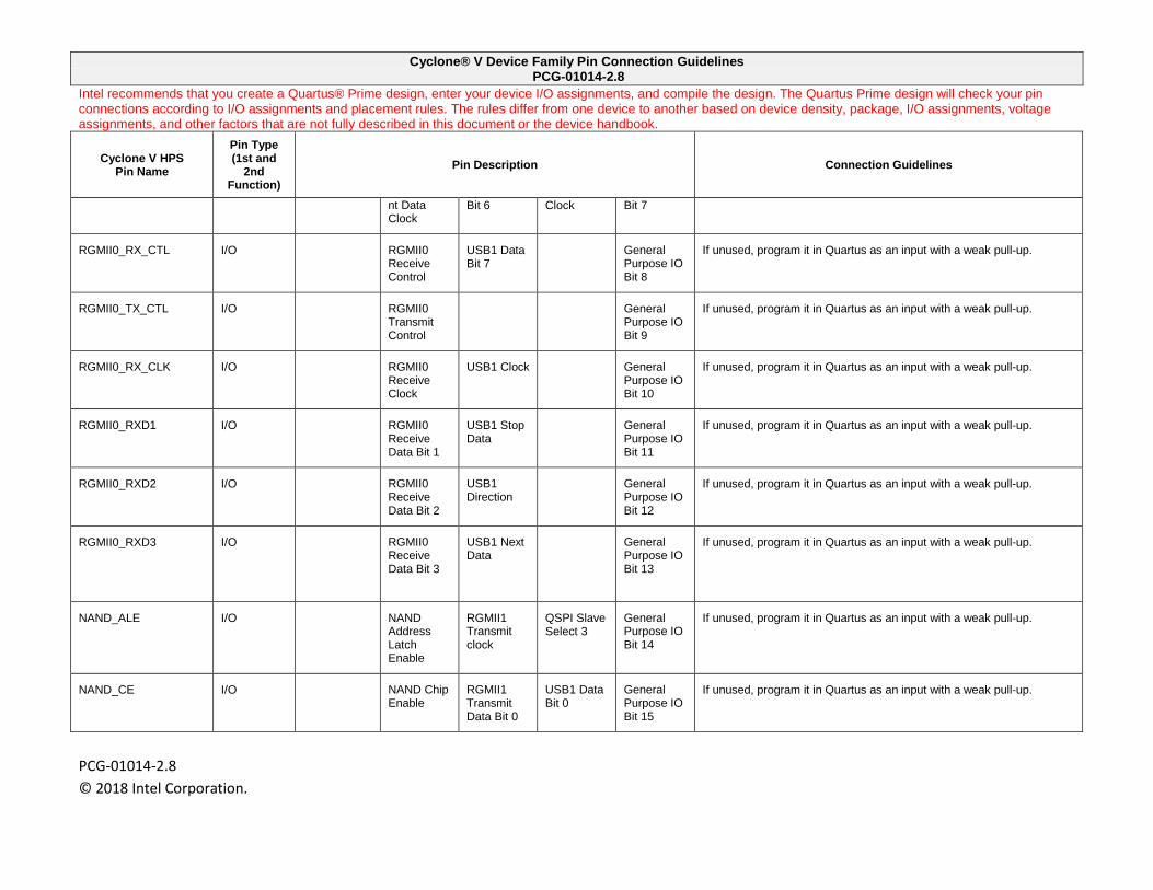
Cyclone® V Device Family Pin Connection Guidelines PCG-01014-2.8
Intel recommends that you create a Quartus® Prime design, enter your device I/O assignments, and compile the design. The Quartus Prime design will check your pin connections according to I/O assignments and placement rules. The rules differ from one device to another based on device density, package, I/O assignments, voltage assignments, and other factors that are not fully described in this document or the device handbook.
PCG-01014-2.8 © 2018 Intel Corporation.
Cyclone V HPS Pin Name
Pin Type (1st and
2nd Function)
Pin Description Connection Guidelines
nt Data Clock
Bit 6 Clock Bit 7
RGMII0_RX_CTL I/O RGMII0 Receive Control
USB1 Data Bit 7
General Purpose IO Bit 8
If unused, program it in Quartus as an input with a weak pull-up.
RGMII0_TX_CTL I/O RGMII0 Transmit Control
General Purpose IO Bit 9
If unused, program it in Quartus as an input with a weak pull-up.
RGMII0_RX_CLK I/O RGMII0 Receive Clock
USB1 Clock General Purpose IO Bit 10
If unused, program it in Quartus as an input with a weak pull-up.
RGMII0_RXD1 I/O RGMII0 Receive Data Bit 1
USB1 Stop Data
General Purpose IO Bit 11
If unused, program it in Quartus as an input with a weak pull-up.
RGMII0_RXD2 I/O RGMII0 Receive Data Bit 2
USB1 Direction
General Purpose IO Bit 12
If unused, program it in Quartus as an input with a weak pull-up.
RGMII0_RXD3 I/O RGMII0 Receive Data Bit 3
USB1 Next Data
General Purpose IO Bit 13
If unused, program it in Quartus as an input with a weak pull-up.
NAND_ALE I/O NAND Address Latch Enable
RGMII1 Transmit clock
QSPI Slave Select 3
General Purpose IO Bit 14
If unused, program it in Quartus as an input with a weak pull-up.
NAND_CE I/O NAND Chip Enable
RGMII1 Transmit Data Bit 0
USB1 Data Bit 0
General Purpose IO Bit 15
If unused, program it in Quartus as an input with a weak pull-up.
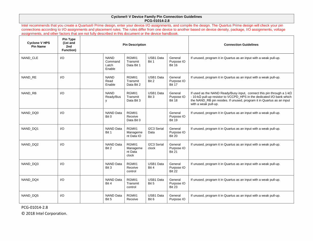
Cyclone® V Device Family Pin Connection Guidelines PCG-01014-2.8
Intel recommends that you create a Quartus® Prime design, enter your device I/O assignments, and compile the design. The Quartus Prime design will check your pin connections according to I/O assignments and placement rules. The rules differ from one device to another based on device density, package, I/O assignments, voltage assignments, and other factors that are not fully described in this document or the device handbook.
PCG-01014-2.8 © 2018 Intel Corporation.
Cyclone V HPS Pin Name
Pin Type (1st and
2nd Function)
Pin Description Connection Guidelines
NAND_CLE I/O NAND Command Latch Enable
RGMII1 Transmit Data Bit 1
USB1 Data Bit 1
General Purpose IO Bit 16
If unused, program it in Quartus as an input with a weak pull-up.
NAND_RE I/O NAND Read Enable
RGMII1 Transmit Data Bit 2
USB1 Data Bit 2
General Purpose IO Bit 17
If unused, program it in Quartus as an input with a weak pull-up.
NAND_RB I/O NAND Ready/Busy
RGMII1 Transmit Data Bit 3
USB1 Data Bit 3
General Purpose IO Bit 18
If used as the NAND Ready/Busy input, connect this pin through a 1-kΩ - 10-kΩ pull-up resistor to VCCPD_HPS in the dedicated I/O bank which the NAND_RB pin resides. If unused, program it in Quartus as an input with a weak pull-up.
NAND_DQ0 I/O NAND Data Bit 0
RGMII1 Receive Data Bit 0
General Purpose IO Bit 19
If unused, program it in Quartus as an input with a weak pull-up.
NAND_DQ1 I/O NAND Data Bit 1
RGMII1 Management Data IO
I2C3 Serial Data
General Purpose IO Bit 20
If unused, program it in Quartus as an input with a weak pull-up.
NAND_DQ2 I/O NAND Data Bit 2
RGMII1 Management Data clock
I2C3 Serial clock
General Purpose IO Bit 21
If unused, program it in Quartus as an input with a weak pull-up.
NAND_DQ3 I/O NAND Data Bit 3
RGMII1 Receive control
USB1 Data Bit 4
General Purpose IO Bit 22
If unused, program it in Quartus as an input with a weak pull-up.
NAND_DQ4 I/O NAND Data Bit 4
RGMII1 Transmit control
USB1 Data Bit 5
General Purpose IO Bit 23
If unused, program it in Quartus as an input with a weak pull-up.
NAND_DQ5 I/O NAND Data Bit 5
RGMII1 Receive
USB1 Data Bit 6
General Purpose IO
If unused, program it in Quartus as an input with a weak pull-up.
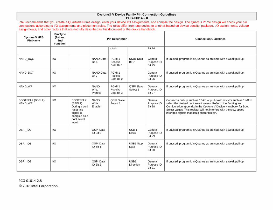
Cyclone® V Device Family Pin Connection Guidelines PCG-01014-2.8
Intel recommends that you create a Quartus® Prime design, enter your device I/O assignments, and compile the design. The Quartus Prime design will check your pin connections according to I/O assignments and placement rules. The rules differ from one device to another based on device density, package, I/O assignments, voltage assignments, and other factors that are not fully described in this document or the device handbook.
PCG-01014-2.8 © 2018 Intel Corporation.
Cyclone V HPS Pin Name
Pin Type (1st and
2nd Function)
Pin Description Connection Guidelines
clock Bit 24
NAND_DQ6 I/O NAND Data Bit 6
RGMII1 Receive Data Bit 1
USB1 Data Bit 7
General Purpose IO Bit 25
If unused, program it in Quartus as an input with a weak pull-up.
NAND_DQ7 I/O NAND Data Bit 7
RGMII1 Receive Data Bit 2
General Purpose IO Bit 26
If unused, program it in Quartus as an input with a weak pull-up.
NAND_WP I/O NAND Write Protect
RGMII1 Receive Data Bit 3
QSPI Slave Select 2
General Purpose IO Bit 27
If unused, program it in Quartus as an input with a weak pull-up.
BOOTSEL2 (BSEL2)/ NAND_WE
I/O BOOTSEL2 (BSEL2) During a cold reset this signal is sampled as a boot select input.
NAND Write Enable
QSPI Slave Select 1
General Purpose IO Bit 28
Connect a pull-up such as 10-kΩ or pull-down resistor such as 1-kΩ to select the desired boot select values. Refer to the Booting and Configuration appendix in the Cyclone V Device Handbook for Boot Select values. This resistor will not interfere with the slow speed interface signals that could share this pin.
QSPI_IO0 I/O QSPI Data IO Bit 0
USB 1 Clock
General Purpose IO Bit 29
If unused, program it in Quartus as an input with a weak pull-up.
QSPI_IO1 I/O QSPI Data IO Bit 1
USB1 Stop Data
General Purpose IO Bit 30
If unused, program it in Quartus as an input with a weak pull-up.
QSPI_IO2 I/O QSPI Data IO Bit 2
USB1 Direction
General Purpose IO Bit 31
If unused, program it in Quartus as an input with a weak pull-up.
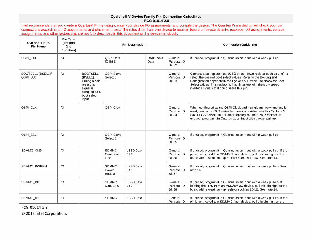
Cyclone® V Device Family Pin Connection Guidelines PCG-01014-2.8
Intel recommends that you create a Quartus® Prime design, enter your device I/O assignments, and compile the design. The Quartus Prime design will check your pin connections according to I/O assignments and placement rules. The rules differ from one device to another based on device density, package, I/O assignments, voltage assignments, and other factors that are not fully described in this document or the device handbook.
PCG-01014-2.8 © 2018 Intel Corporation.
Cyclone V HPS Pin Name
Pin Type (1st and
2nd Function)
Pin Description Connection Guidelines
QSPI_IO3 I/O QSPI Data IO Bit 3
USB1 Next Data
General Purpose IO Bit 32
If unused, program it in Quartus as an input with a weak pull-up.
BOOTSEL1 (BSEL1)/ QSPI_SS0
I/O BOOTSEL1 (BSEL1) During a cold reset this signal is sampled as a boot select input.
QSPI Slave Select 0
General Purpose IO Bit 33
Connect a pull-up such as 10-kΩ or pull-down resistor such as 1-kΩ to select the desired boot select values. Refer to the Booting and Configuration appendix in the Cyclone V Device Handbook for Boot Select values. This resistor will not interfere with the slow speed interface signals that could share this pin.
QSPI_CLK I/O QSPI Clock General Purpose IO Bit 34
When configured as the QSPI Clock and if single memory topology is used, connect a 50 Ω series termination resistor near this Cyclone V SoC FPGA device pin.For other topologies use a 25 Ω resistor. If unused, program it in Quartus as an input with a weak pull-up.
QSPI_SS1 I/O QSPI Slave Select 1
General Purpose IO Bit 35
If unused, program it in Quartus as an input with a weak pull-up.
SDMMC_CMD I/O SDMMC Command Line
USB0 Data Bit 0
General Purpose IO Bit 36
If unused, program it in Quartus as an input with a weak pull-up. If the pin is connected to a SD/MMC flash device, pull this pin high on the board with a weak pull-up resistor such as 10-kΩ. See note 14.
SDMMC_PWREN I/O SDMMC Power Enable
USB0 Data Bit 1
General Purpose IO Bit 37
If unused, program it in Quartus as an input with a weak pull-up. See note 14.
SDMMC_D0 I/O SDMMC Data Bit 0
USB0 Data Bit 2
General Purpose IO Bit 38
If unused, program it in Quartus as an input with a weak pull-up. If booting the HPS from an MMC/eMMC device, pull this pin high on the board with a weak pull-up resistor such as 10-kΩ. See note 14.
SDMMC_D1 I/O SDMMC USB0 Data General Purpose IO
If unused, program it in Quartus as an input with a weak pull-up. If the pin is connected to a SD/MMC flash device, pull this pin high on the
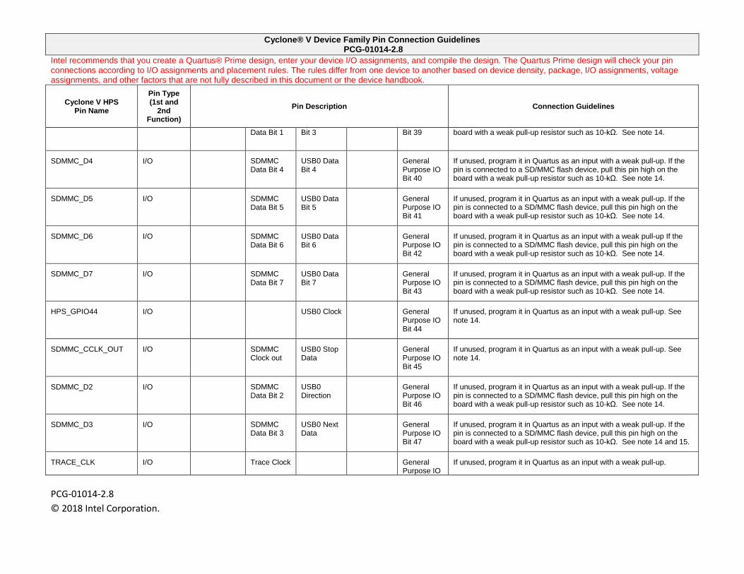
Cyclone® V Device Family Pin Connection Guidelines PCG-01014-2.8
Intel recommends that you create a Quartus® Prime design, enter your device I/O assignments, and compile the design. The Quartus Prime design will check your pin connections according to I/O assignments and placement rules. The rules differ from one device to another based on device density, package, I/O assignments, voltage assignments, and other factors that are not fully described in this document or the device handbook.
PCG-01014-2.8 © 2018 Intel Corporation.
Cyclone V HPS Pin Name
Pin Type (1st and
2nd Function)
Pin Description Connection Guidelines
Data Bit 1 Bit 3 Bit 39 board with a weak pull-up resistor such as 10-kΩ. See note 14.
SDMMC_D4 I/O SDMMC Data Bit 4
USB0 Data Bit 4
General Purpose IO Bit 40
If unused, program it in Quartus as an input with a weak pull-up. If the pin is connected to a SD/MMC flash device, pull this pin high on the board with a weak pull-up resistor such as 10-kΩ. See note 14.
SDMMC_D5 I/O SDMMC Data Bit 5
USB0 Data Bit 5
General Purpose IO Bit 41
If unused, program it in Quartus as an input with a weak pull-up. If the pin is connected to a SD/MMC flash device, pull this pin high on the board with a weak pull-up resistor such as 10-kΩ. See note 14.
SDMMC_D6 I/O SDMMC Data Bit 6
USB0 Data Bit 6
General Purpose IO Bit 42
If unused, program it in Quartus as an input with a weak pull-up If the pin is connected to a SD/MMC flash device, pull this pin high on the board with a weak pull-up resistor such as 10-kΩ. See note 14.
SDMMC_D7 I/O SDMMC Data Bit 7
USB0 Data Bit 7
General Purpose IO Bit 43
If unused, program it in Quartus as an input with a weak pull-up. If the pin is connected to a SD/MMC flash device, pull this pin high on the board with a weak pull-up resistor such as 10-kΩ. See note 14.
HPS_GPIO44 I/O USB0 Clock General Purpose IO Bit 44
If unused, program it in Quartus as an input with a weak pull-up. See note 14.
SDMMC_CCLK_OUT I/O SDMMC Clock out
USB0 Stop Data
General Purpose IO Bit 45
If unused, program it in Quartus as an input with a weak pull-up. See note 14.
SDMMC_D2 I/O SDMMC Data Bit 2
USB0 Direction
General Purpose IO Bit 46
If unused, program it in Quartus as an input with a weak pull-up. If the pin is connected to a SD/MMC flash device, pull this pin high on the board with a weak pull-up resistor such as 10-kΩ. See note 14.
SDMMC_D3 I/O SDMMC Data Bit 3
USB0 Next Data
General Purpose IO Bit 47
If unused, program it in Quartus as an input with a weak pull-up. If the pin is connected to a SD/MMC flash device, pull this pin high on the board with a weak pull-up resistor such as 10-kΩ. See note 14 and 15.
TRACE_CLK I/O Trace Clock General Purpose IO
If unused, program it in Quartus as an input with a weak pull-up.
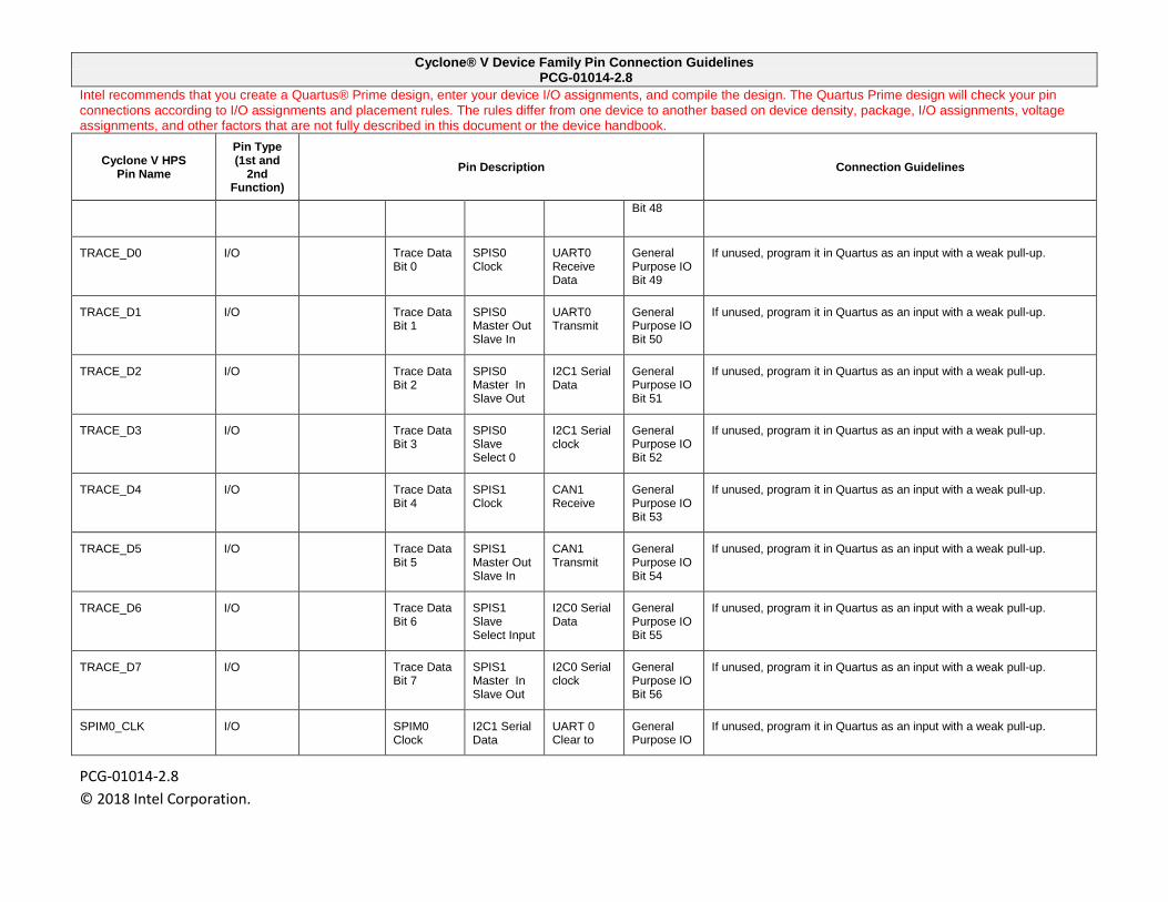
Cyclone® V Device Family Pin Connection Guidelines PCG-01014-2.8
Intel recommends that you create a Quartus® Prime design, enter your device I/O assignments, and compile the design. The Quartus Prime design will check your pin connections according to I/O assignments and placement rules. The rules differ from one device to another based on device density, package, I/O assignments, voltage assignments, and other factors that are not fully described in this document or the device handbook.
PCG-01014-2.8 © 2018 Intel Corporation.
Cyclone V HPS Pin Name
Pin Type (1st and
2nd Function)
Pin Description Connection Guidelines
Bit 48
TRACE_D0 I/O Trace Data Bit 0
SPIS0 Clock
UART0 Receive Data
General Purpose IO Bit 49
If unused, program it in Quartus as an input with a weak pull-up.
TRACE_D1 I/O Trace Data Bit 1
SPIS0 Master Out Slave In
UART0 Transmit
General Purpose IO Bit 50
If unused, program it in Quartus as an input with a weak pull-up.
TRACE_D2 I/O Trace Data Bit 2
SPIS0 Master In Slave Out
I2C1 Serial Data
General Purpose IO Bit 51
If unused, program it in Quartus as an input with a weak pull-up.
TRACE_D3 I/O Trace Data Bit 3
SPIS0 Slave Select 0
I2C1 Serial clock
General Purpose IO Bit 52
If unused, program it in Quartus as an input with a weak pull-up.
TRACE_D4 I/O Trace Data Bit 4
SPIS1 Clock
CAN1 Receive
General Purpose IO Bit 53
If unused, program it in Quartus as an input with a weak pull-up.
TRACE_D5 I/O Trace Data Bit 5
SPIS1 Master Out Slave In
CAN1 Transmit
General Purpose IO Bit 54
If unused, program it in Quartus as an input with a weak pull-up.
TRACE_D6 I/O Trace Data Bit 6
SPIS1 Slave Select Input
I2C0 Serial Data
General Purpose IO Bit 55
If unused, program it in Quartus as an input with a weak pull-up.
TRACE_D7 I/O Trace Data Bit 7
SPIS1 Master In Slave Out
I2C0 Serial clock
General Purpose IO Bit 56
If unused, program it in Quartus as an input with a weak pull-up.
SPIM0_CLK I/O SPIM0 Clock
I2C1 Serial Data
UART 0 Clear to
General Purpose IO
If unused, program it in Quartus as an input with a weak pull-up.
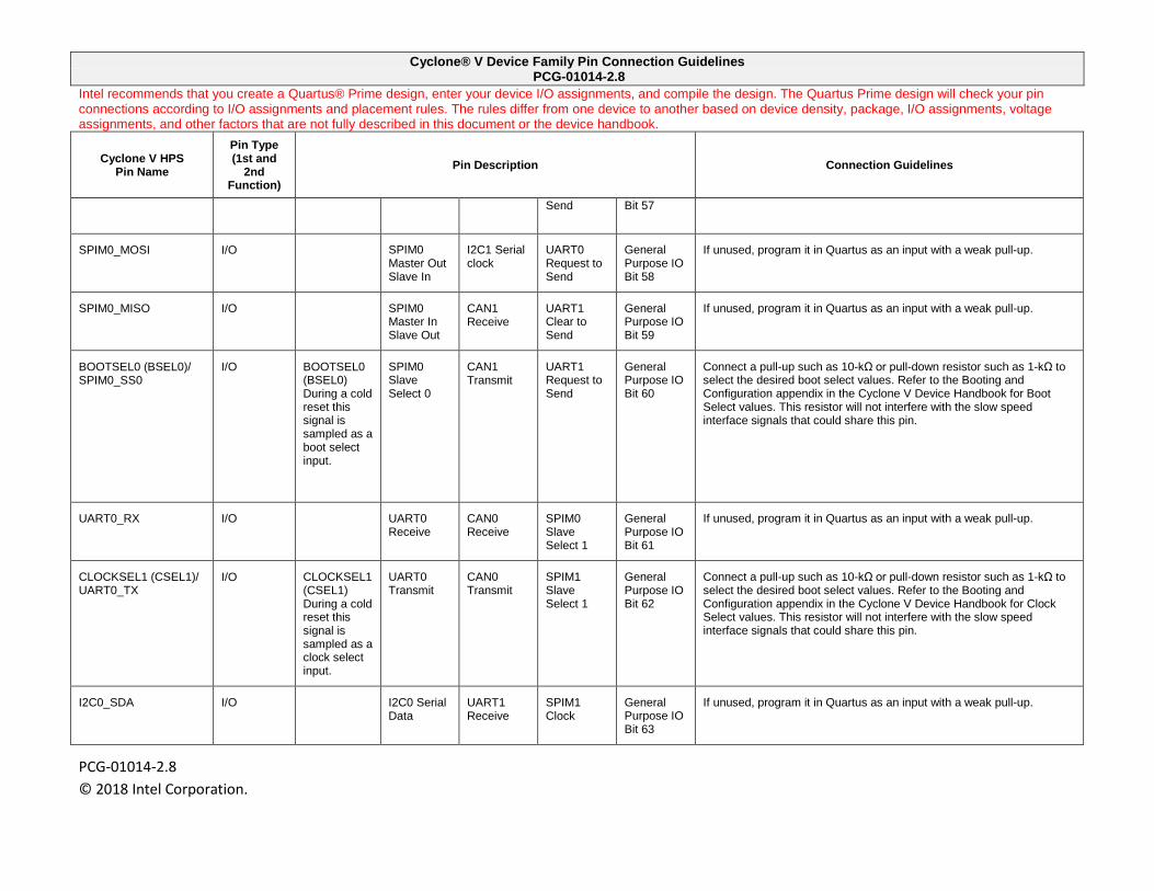
Cyclone® V Device Family Pin Connection Guidelines PCG-01014-2.8
Intel recommends that you create a Quartus® Prime design, enter your device I/O assignments, and compile the design. The Quartus Prime design will check your pin connections according to I/O assignments and placement rules. The rules differ from one device to another based on device density, package, I/O assignments, voltage assignments, and other factors that are not fully described in this document or the device handbook.
PCG-01014-2.8 © 2018 Intel Corporation.
Cyclone V HPS Pin Name
Pin Type (1st and
2nd Function)
Pin Description Connection Guidelines
Send Bit 57
SPIM0_MOSI I/O SPIM0 Master Out Slave In
I2C1 Serial clock
UART0 Request to Send
General Purpose IO Bit 58
If unused, program it in Quartus as an input with a weak pull-up.
SPIM0_MISO I/O SPIM0 Master In Slave Out
CAN1 Receive
UART1 Clear to Send
General Purpose IO Bit 59
If unused, program it in Quartus as an input with a weak pull-up.
BOOTSEL0 (BSEL0)/ SPIM0_SS0
I/O BOOTSEL0 (BSEL0) During a cold reset this signal is sampled as a boot select input.
SPIM0 Slave Select 0
CAN1 Transmit
UART1 Request to Send
General Purpose IO Bit 60
Connect a pull-up such as 10-kΩ or pull-down resistor such as 1-kΩ to select the desired boot select values. Refer to the Booting and Configuration appendix in the Cyclone V Device Handbook for Boot Select values. This resistor will not interfere with the slow speed interface signals that could share this pin.
UART0_RX I/O UART0 Receive
CAN0 Receive
SPIM0 Slave Select 1
General Purpose IO Bit 61
If unused, program it in Quartus as an input with a weak pull-up.
CLOCKSEL1 (CSEL1)/ UART0_TX
I/O CLOCKSEL1(CSEL1) During a cold reset this signal is sampled as a clock select input.
UART0 Transmit
CAN0 Transmit
SPIM1 Slave Select 1
General Purpose IO Bit 62
Connect a pull-up such as 10-kΩ or pull-down resistor such as 1-kΩ to select the desired boot select values. Refer to the Booting and Configuration appendix in the Cyclone V Device Handbook for Clock Select values. This resistor will not interfere with the slow speed interface signals that could share this pin.
I2C0_SDA I/O I2C0 Serial Data
UART1 Receive
SPIM1 Clock
General Purpose IO Bit 63
If unused, program it in Quartus as an input with a weak pull-up.
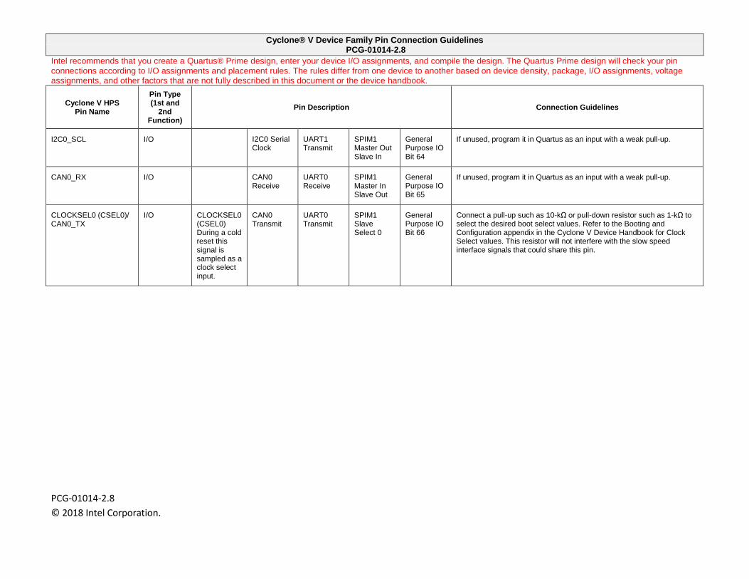
Cyclone® V Device Family Pin Connection Guidelines PCG-01014-2.8
Intel recommends that you create a Quartus® Prime design, enter your device I/O assignments, and compile the design. The Quartus Prime design will check your pin connections according to I/O assignments and placement rules. The rules differ from one device to another based on device density, package, I/O assignments, voltage assignments, and other factors that are not fully described in this document or the device handbook.
PCG-01014-2.8 © 2018 Intel Corporation.
Cyclone V HPS Pin Name
Pin Type (1st and
2nd Function)
Pin Description Connection Guidelines
I2C0_SCL I/O I2C0 Serial Clock
UART1 Transmit
SPIM1 Master Out Slave In
General Purpose IO Bit 64
If unused, program it in Quartus as an input with a weak pull-up.
CAN0_RX I/O CAN0 Receive
UART0 Receive
SPIM1 Master In Slave Out
General Purpose IO Bit 65
If unused, program it in Quartus as an input with a weak pull-up.
CLOCKSEL0 (CSEL0)/ CAN0_TX
I/O CLOCKSEL0(CSEL0) During a cold reset this signal is sampled as a clock select input.
CAN0 Transmit
UART0 Transmit
SPIM1 Slave Select 0
General Purpose IO Bit 66
Connect a pull-up such as 10-kΩ or pull-down resistor such as 1-kΩ to select the desired boot select values. Refer to the Booting and Configuration appendix in the Cyclone V Device Handbook for Clock Select values. This resistor will not interfere with the slow speed interface signals that could share this pin.
Cyclone® V Device Family Pin Connection Guidelines PCG-01014-2.8
Intel recommends that you create a Quartus® Prime design, enter your device I/O assignments, and compile the design. The Quartus Prime design will check your pin connections according to I/O assignments and placement rules. The rules differ from one device to another based on device density, package, I/O assignments, voltage assignments, and other factors that are not fully described in this document or the device handbook.
PCG-01014-2.8 © 2018 Intel Corporation.
Intel provides these guidelines only as recommendations. It is the responsibility of the designer to apply simulation results to the design to verify proper device functionality. 1. These pin connection guidelines are based on the Cyclone V SX, ST, and SE device variants. 2. Capacitance values for the power supply should be selected after considering the amount of power they need to supply over the frequency of operation of the particular circuit being
decoupled. A target impedance for the power plane should be calculated based on current draw and voltage droop requirements of the device/supply. The power plane should then be decoupled using the appropriate number of capacitors. On-board capacitors do not decouple higher than 100 MHz because “Equivalent Series Inductance” of the mounting of the packages. Proper board design techniques such as interplane capacitance with low inductance should be considered for higher frequency decoupling. The Power Delivery Network (PDN) tool serves as an excellent decoupling analysis tool. For more details, refer to the
3. Use the Cyclone V Early Power Estimator to determine the current requirements for VCC and other power supplies. 4. These supplies may share power planes across multiple Cyclone V devices. 5. Example 4, Figure 4, Example 5, Figure 5, Example 6, and Figure 6 illustrate power supply sharing guidelines for the Cyclone V SX device.
Example 7, Figure 7, Example 8, and Figure 8 illustrate power supply sharing guidelines for the Cyclone V ST device. Example 9, Figure 9, Example 10, Figure 10, Example 11, and Figure 11 illustrate power supply sharing guidelines for the Cyclone V SE device.
6. Power pins should not share breakout vias from the BGA. Each ball on the BGA needs to have its own dedicated breakout via. VCC must not share breakout vias. 7. Low Noise Switching Regulator - defined as a switching regulator circuit encapsulated in a thin surface mount package containing the switch controller, power FETs, inductor, and
other support components. The switching frequency is usually between 800kHz and 1MHz and has fast transient response. The switching frequency range is not an Intel requirement. However, Intel does require the Line Regulation and Load Regulation meet the following specifications: • Line Regulation < 0.4% • Load Regulation < 1.2%
8. The number of modular I/O banks on Cyclone V devices depends on the device density. For the indexes available for a specific device, please refer to the I/O Bank section in the Cyclone V device handbook.
9. For AC-coupled links, the AC-coupling capacitor can be placed anywhere along the channel. PCIe protocol requires the AC-coupling capacitor to be placed on the transmitter side of the interface that permits adapters to be plugged and unplugged.
10. All transceiver power pins except VCCH_GXBL pin on the same side of the device must be connected either to the required supply or to GND. When ALL transceiver channels on the same side are unused, you have the option to connect all of the transceiver power pins except VCCH_GXBL pin on the same side of the device to GND or to the required supply. The VCCH_GXBL pin must always be powered.
11. For item [#] Please refer to the device pin table for the pin-out mapping. 12. The peripheral pins are programmable through pin multiplexers. Each pin may have up to four functions. Configuration of each pin is done during HPS configuration. 13. Peripheral I/O pins and GPIO pins that are configured as Loan I/O drives '1' before FPGA is being configured. 14. USB0 is not available in U19 package with 484 pin count. 15. When using SD card, there is an existing 50-kΩ pull-up on SDMMC Data Bit 3 that can be disabled using SET_CLR_CARD_DETECT (ACMD42) command. This does not apply to
eMMC flash.
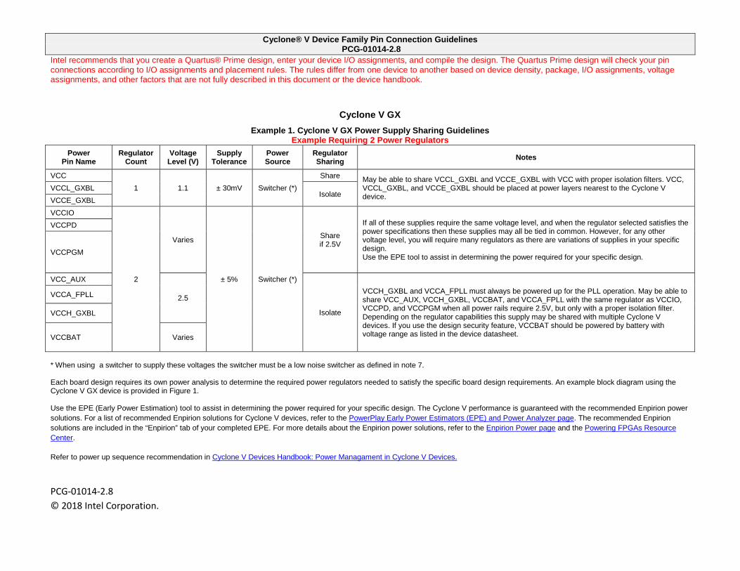
Cyclone® V Device Family Pin Connection Guidelines PCG-01014-2.8
Intel recommends that you create a Quartus® Prime design, enter your device I/O assignments, and compile the design. The Quartus Prime design will check your pin connections according to I/O assignments and placement rules. The rules differ from one device to another based on device density, package, I/O assignments, voltage assignments, and other factors that are not fully described in this document or the device handbook.
PCG-01014-2.8 © 2018 Intel Corporation.
Cyclone V GX Example 1. Cyclone V GX Power Supply Sharing Guidelines
Example Requiring 2 Power Regulators Power
Pin Name Regulator
Count Voltage
Level (V) Supply
Tolerance Power Source
Regulator Sharing Notes
VCC 1 1.1 ± 30mV Switcher (*)
Share May be able to share VCCL_GXBL and VCCE_GXBL with VCC with proper isolation filters. VCC, VCCL_GXBL, and VCCE_GXBL should be placed at power layers nearest to the Cyclone V device.
VCCL_GXBL Isolate
VCCE_GXBL VCCIO
2
Varies
± 5% Switcher (*)
Share if 2.5V
If all of these supplies require the same voltage level, and when the regulator selected satisfies the power specifications then these supplies may all be tied in common. However, for any other voltage level, you will require many regulators as there are variations of supplies in your specific design. Use the EPE tool to assist in determining the power required for your specific design.
VCCPD
VCCPGM
VCC_AUX
2.5
Isolate
VCCH_GXBL and VCCA_FPLL must always be powered up for the PLL operation. May be able to share VCC_AUX, VCCH_GXBL, VCCBAT, and VCCA_FPLL with the same regulator as VCCIO, VCCPD, and VCCPGM when all power rails require 2.5V, but only with a proper isolation filter. Depending on the regulator capabilities this supply may be shared with multiple Cyclone V devices. If you use the design security feature, VCCBAT should be powered by battery with voltage range as listed in the device datasheet.
VCCA_FPLL
VCCH_GXBL
VCCBAT Varies
* When using a switcher to supply these voltages the switcher must be a low noise switcher as defined in note 7. Each board design requires its own power analysis to determine the required power regulators needed to satisfy the specific board design requirements. An example block diagram using the Cyclone V GX device is provided in Figure 1. Use the EPE (Early Power Estimation) tool to assist in determining the power required for your specific design. The Cyclone V performance is guaranteed with the recommended Enpirion power solutions. For a list of recommended Enpirion solutions for Cyclone V devices, refer to the PowerPlay Early Power Estimators (EPE) and Power Analyzer page. The recommended Enpirion solutions are included in the “Enpirion” tab of your completed EPE. For more details about the Enpirion power solutions, refer to the Enpirion Power page and the Powering FPGAs Resource Center.
Refer to power up sequence recommendation in Cyclone V Devices Handbook: Power Managament in Cyclone V Devices.
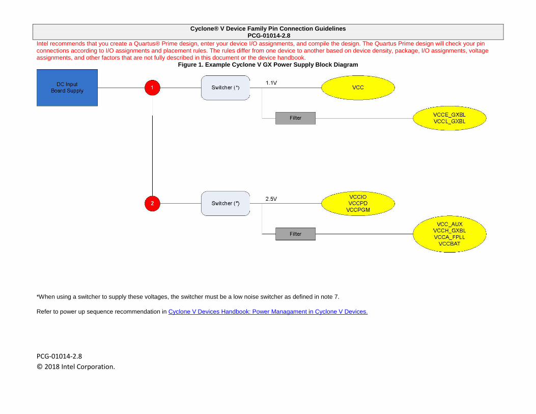
Cyclone® V Device Family Pin Connection Guidelines PCG-01014-2.8
Intel recommends that you create a Quartus® Prime design, enter your device I/O assignments, and compile the design. The Quartus Prime design will check your pin connections according to I/O assignments and placement rules. The rules differ from one device to another based on device density, package, I/O assignments, voltage assignments, and other factors that are not fully described in this document or the device handbook.
PCG-01014-2.8 © 2018 Intel Corporation.
Figure 1. Example Cyclone V GX Power Supply Block Diagram
*When using a switcher to supply these voltages, the switcher must be a low noise switcher as defined in note 7.
Refer to power up sequence recommendation in Cyclone V Devices Handbook: Power Managament in Cyclone V Devices.
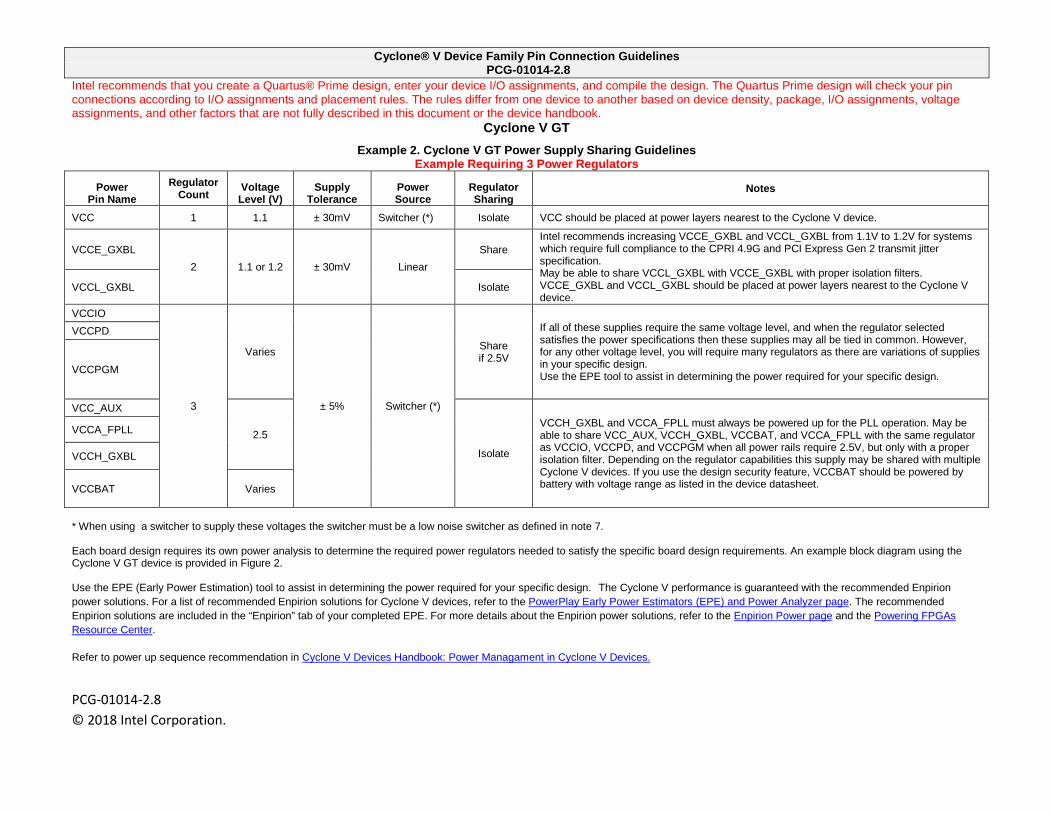
Cyclone® V Device Family Pin Connection Guidelines PCG-01014-2.8
Intel recommends that you create a Quartus® Prime design, enter your device I/O assignments, and compile the design. The Quartus Prime design will check your pin connections according to I/O assignments and placement rules. The rules differ from one device to another based on device density, package, I/O assignments, voltage assignments, and other factors that are not fully described in this document or the device handbook.
PCG-01014-2.8 © 2018 Intel Corporation.
Cyclone V GT Example 2. Cyclone V GT Power Supply Sharing Guidelines
Example Requiring 3 Power Regulators
Power Pin Name
Regulator Count Voltage
Level (V) Supply
Tolerance Power Source
Regulator Sharing
Notes
VCC 1 1.1 ± 30mV Switcher (*) Isolate VCC should be placed at power layers nearest to the Cyclone V device.
VCCE_GXBL 2 1.1 or 1.2 ± 30mV Linear
Share Intel recommends increasing VCCE_GXBL and VCCL_GXBL from 1.1V to 1.2V for systems which require full compliance to the CPRI 4.9G and PCI Express Gen 2 transmit jitter specification. May be able to share VCCL_GXBL with VCCE_GXBL with proper isolation filters. VCCE_GXBL and VCCL_GXBL should be placed at power layers nearest to the Cyclone V device.
VCCL_GXBL Isolate
VCCIO
3
Varies
± 5% Switcher (*)
Share if 2.5V
If all of these supplies require the same voltage level, and when the regulator selected satisfies the power specifications then these supplies may all be tied in common. However, for any other voltage level, you will require many regulators as there are variations of supplies in your specific design. Use the EPE tool to assist in determining the power required for your specific design.
VCCPD
VCCPGM
VCC_AUX
2.5
Isolate
VCCH_GXBL and VCCA_FPLL must always be powered up for the PLL operation. May be able to share VCC_AUX, VCCH_GXBL, VCCBAT, and VCCA_FPLL with the same regulator as VCCIO, VCCPD, and VCCPGM when all power rails require 2.5V, but only with a proper isolation filter. Depending on the regulator capabilities this supply may be shared with multiple Cyclone V devices. If you use the design security feature, VCCBAT should be powered by battery with voltage range as listed in the device datasheet.
VCCA_FPLL
VCCH_GXBL
VCCBAT Varies
* When using a switcher to supply these voltages the switcher must be a low noise switcher as defined in note 7. Each board design requires its own power analysis to determine the required power regulators needed to satisfy the specific board design requirements. An example block diagram using the Cyclone V GT device is provided in Figure 2. Use the EPE (Early Power Estimation) tool to assist in determining the power required for your specific design. The Cyclone V performance is guaranteed with the recommended Enpirion power solutions. For a list of recommended Enpirion solutions for Cyclone V devices, refer to the PowerPlay Early Power Estimators (EPE) and Power Analyzer page. The recommended Enpirion solutions are included in the “Enpirion” tab of your completed EPE. For more details about the Enpirion power solutions, refer to the Enpirion Power page and the Powering FPGAs Resource Center.
Refer to power up sequence recommendation in Cyclone V Devices Handbook: Power Managament in Cyclone V Devices.
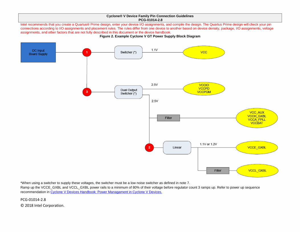
Cyclone® V Device Family Pin Connection Guidelines PCG-01014-2.8
Intel recommends that you create a Quartus® Prime design, enter your device I/O assignments, and compile the design. The Quartus Prime design will check your pin connections according to I/O assignments and placement rules. The rules differ from one device to another based on device density, package, I/O assignments, voltage assignments, and other factors that are not fully described in this document or the device handbook.
PCG-01014-2.8 © 2018 Intel Corporation.
Figure 2. Example Cyclone V GT Power Supply Block Diagram
*When using a switcher to supply these voltages, the switcher must be a low noise switcher as defined in note 7. Ramp up the VCCE_GXBL and VCCL_GXBL power rails to a minimum of 80% of their voltage before regulator count 3 ramps up. Refer to power up sequence recommendation in Cyclone V Devices Handbook: Power Managament in Cyclone V Devices.
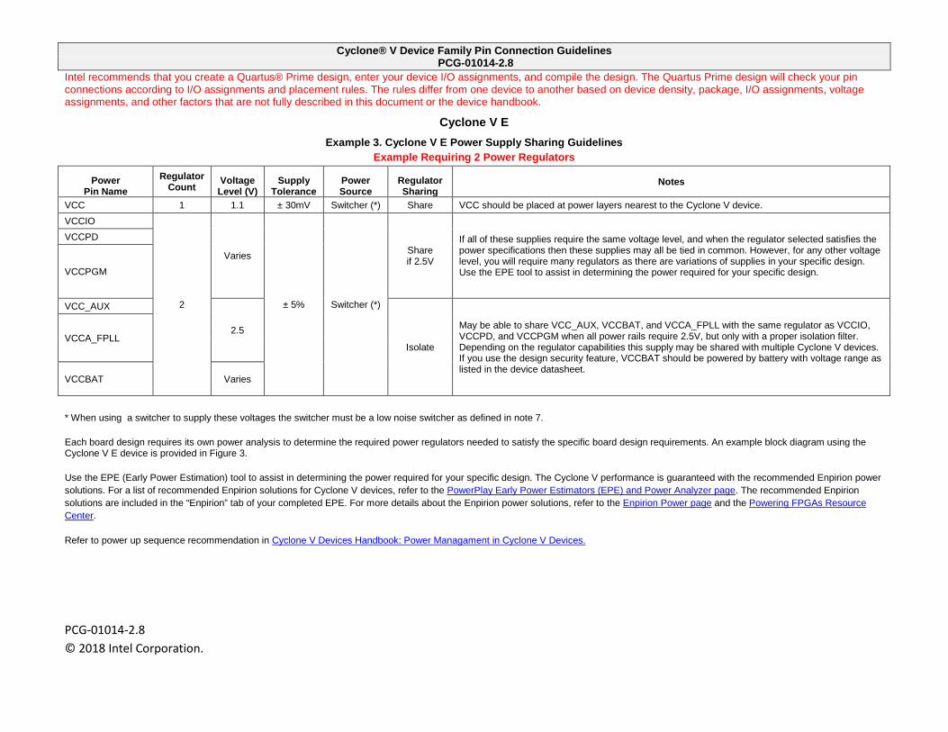
Cyclone® V Device Family Pin Connection Guidelines PCG-01014-2.8
Intel recommends that you create a Quartus® Prime design, enter your device I/O assignments, and compile the design. The Quartus Prime design will check your pin connections according to I/O assignments and placement rules. The rules differ from one device to another based on device density, package, I/O assignments, voltage assignments, and other factors that are not fully described in this document or the device handbook.
PCG-01014-2.8 © 2018 Intel Corporation.
Cyclone V E Example 3. Cyclone V E Power Supply Sharing Guidelines
Example Requiring 2 Power Regulators
Power Pin Name
Regulator Count Voltage
Level (V) Supply
Tolerance Power Source
Regulator Sharing
Notes
VCC 1 1.1 ± 30mV Switcher (*) Share VCC should be placed at power layers nearest to the Cyclone V device. VCCIO
2
Varies
± 5% Switcher (*)
Share if 2.5V
If all of these supplies require the same voltage level, and when the regulator selected satisfies the power specifications then these supplies may all be tied in common. However, for any other voltage level, you will require many regulators as there are variations of supplies in your specific design. Use the EPE tool to assist in determining the power required for your specific design.
VCCPD
VCCPGM
VCC_AUX
2.5
Isolate
May be able to share VCC_AUX, VCCBAT, and VCCA_FPLL with the same regulator as VCCIO, VCCPD, and VCCPGM when all power rails require 2.5V, but only with a proper isolation filter. Depending on the regulator capabilities this supply may be shared with multiple Cyclone V devices. If you use the design security feature, VCCBAT should be powered by battery with voltage range as listed in the device datasheet.
VCCA_FPLL
VCCBAT Varies
* When using a switcher to supply these voltages the switcher must be a low noise switcher as defined in note 7. Each board design requires its own power analysis to determine the required power regulators needed to satisfy the specific board design requirements. An example block diagram using the Cyclone V E device is provided in Figure 3. Use the EPE (Early Power Estimation) tool to assist in determining the power required for your specific design. The Cyclone V performance is guaranteed with the recommended Enpirion power solutions. For a list of recommended Enpirion solutions for Cyclone V devices, refer to the PowerPlay Early Power Estimators (EPE) and Power Analyzer page. The recommended Enpirion solutions are included in the “Enpirion” tab of your completed EPE. For more details about the Enpirion power solutions, refer to the Enpirion Power page and the Powering FPGAs Resource Center.
Refer to power up sequence recommendation in Cyclone V Devices Handbook: Power Managament in Cyclone V Devices.
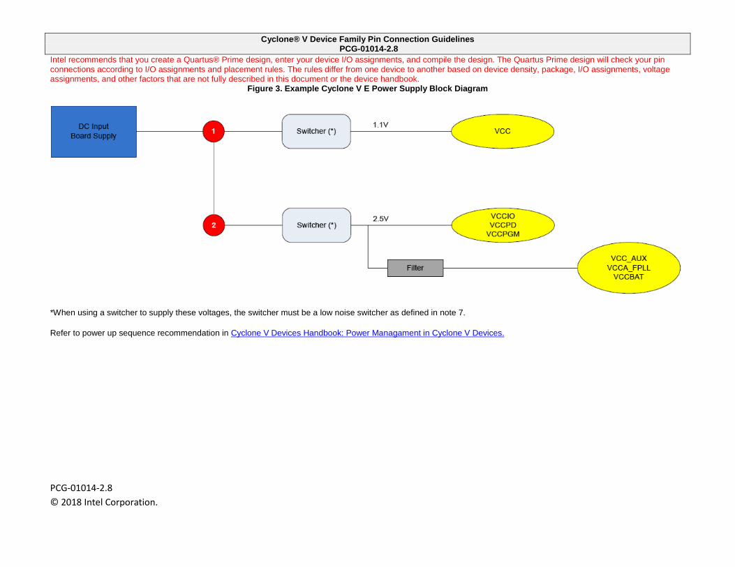
Cyclone® V Device Family Pin Connection Guidelines PCG-01014-2.8
Intel recommends that you create a Quartus® Prime design, enter your device I/O assignments, and compile the design. The Quartus Prime design will check your pin connections according to I/O assignments and placement rules. The rules differ from one device to another based on device density, package, I/O assignments, voltage assignments, and other factors that are not fully described in this document or the device handbook.
PCG-01014-2.8 © 2018 Intel Corporation.
Figure 3. Example Cyclone V E Power Supply Block Diagram
*When using a switcher to supply these voltages, the switcher must be a low noise switcher as defined in note 7.
Refer to power up sequence recommendation in Cyclone V Devices Handbook: Power Managament in Cyclone V Devices.
Cyclone® V Device Family Pin Connection Guidelines PCG-01014-2.8
Intel recommends that you create a Quartus® Prime design, enter your device I/O assignments, and compile the design. The Quartus Prime design will check your pin connections according to I/O assignments and placement rules. The rules differ from one device to another based on device density, package, I/O assignments, voltage assignments, and other factors that are not fully described in this document or the device handbook.
PCG-01014-2.8 © 2018 Intel Corporation.
Cyclone V SX Example 4. Cyclone V SX Power Supply Sharing Guidelines
Example Requiring 2 Power Regulators (FPGA & HPS share power) Power
Pin Name Regulator
Count Voltage Level (V)
Supply Tolerance
Power Source
Regulator Sharing Notes
VCC
1 1.1 ± 30mV Switcher (*)
Share May be able to share VCCL_GXBL and VCCE_GXBL with VCC and VCC_HPS with proper isolation filters. VCC, VCC_HPS, VCCL_GXBL, and VCCE_GXBL should be placed at power layers nearest to the Cyclone V device.
VCC_HPS VCCE_GXBL
Isolate VCCL_GXBL
VCCIO
2
Varies
± 5% Switcher (*)
Share if 2.5V
If all of these supplies require the same voltage level, and when the regulator selected satisfies the power specifications, then these supplies may all be tied in common. However, for any other voltage level, you will require many regulators as there are variations of supplies in your specific design. Use the EPE tool to assist in determining the power required for your specific design.
VCCIO_HPS VCCPD VCCPD_HPS VCCPGM VCCRSTCLK_HPS VCC_AUX
2.5
Isolate
VCC_AUX, VCCA_FPLL, VCCH_GXBL and VCCPLL_HPS must always be powered up for the PLL operation. VCC_AUX_SHARED must always be powered up for the HPS operation. May be able to share VCC_AUX, VCCA_FPLL, VCCH_GXBL, VCCPLL_HPS VCC_AUX_SHARED and VCCBAT with the same regulator as VCCIO, VCCIO_HPS, VCCPD, VCCPD_HPS, VCCPGM and VCCRSTCLK_HPS when all power rails require 2.5V, but only with proper isolation filters. Depending on the regulator capabilities this supply may be shared with multiple Cyclone V devices. If you use the design security feature, VCCBAT should be powered by battery with voltage range as listed in the device datasheet.
VCC_AUX_SHARED VCCA_FPLL VCCH_GXBL
VCCPLL_HPS
VCCBAT Varies
* When using a switcher to supply these voltages the switcher must be a low noise switcher as defined in note 7. Each board design requires its own power analysis to determine the required power regulators needed to satisfy the specific board design requirements. An example block diagram using the Cyclone V SX device is provided in Figure 4. Use the EPE (Early Power Estimation) tool to assist in determining the power required for your specific design. The Cyclone V performance is guaranteed with the recommended Enpirion power solutions. For a list of recommended Enpirion solutions for Cyclone V devices, refer to the PowerPlay Early Power Estimators (EPE) and Power Analyzer page. The recommended Enpirion solutions are included in the “Enpirion” tab of your completed EPE. For more details about the Enpirion power solutions, refer to the Enpirion Power page and the Powering FPGAs Resource Center.
Refer to power up sequence recommendation in Cyclone V Devices Handbook: Power Managament in Cyclone V Devices.
Cyclone® V Device Family Pin Connection Guidelines PCG-01014-2.8
Intel recommends that you create a Quartus® Prime design, enter your device I/O assignments, and compile the design. The Quartus Prime design will check your pin connections according to I/O assignments and placement rules. The rules differ from one device to another based on device density, package, I/O assignments, voltage assignments, and other factors that are not fully described in this document or the device handbook.
PCG-01014-2.8 © 2018 Intel Corporation.
Figure 4. Example Cyclone V SX Power Supply Block Diagram (FPGA and HPS share power)
*When using a switcher to supply these voltages, the switcher must be a low noise switcher as defined in note 7.
Refer to power up sequence recommendation in Cyclone V Devices Handbook: Power Managament in Cyclone V Devices.
Cyclone® V Device Family Pin Connection Guidelines PCG-01014-2.8
Intel recommends that you create a Quartus® Prime design, enter your device I/O assignments, and compile the design. The Quartus Prime design will check your pin connections according to I/O assignments and placement rules. The rules differ from one device to another based on device density, package, I/O assignments, voltage assignments, and other factors that are not fully described in this document or the device handbook.
PCG-01014-2.8 © 2018 Intel Corporation.
Example 5. Cyclone V SX C2/C4 Power Supply Sharing Guidelines Example Requiring 4 Power Regulators (FPGA & HPS do not share power)
Power Pin Name
Regulator Count
Voltage Level (V)
Supply Tolerance
Power Source
Regulator Sharing Notes
VCC 1 1.1 ± 30mV Switcher (*)
Share May be able to share VCCL_GXBL and VCCE_GXBL with VCC with proper isolation filters. VCC, VCCL_GXBL, and VCCE_GXBL should be placed at power layers nearest to the Cyclone V device. VCCE_GXBL
Isolate VCCL_GXBL VCCIO
2
Varies
± 5% Switcher (*)
Share if 2.5V
If all of these supplies require the same voltage level, and when the regulator selected satisfies the power specifications then these supplies may all be tied in common. However, for any other voltage level, you will require many regulators as there are variations of supplies in your specific design. Use the EPE tool to assist in determining the power required for your specific design.
VCCPD
VCCPGM
VCC_AUX
2.5 Isolate
VCC_AUX, VCCH_GXBL and VCCA_FPLL must always be powered up for the PLL operation. May be able to share VCCH_GXBL, VCCA_FPLL and VCCBAT with the same regulator as VCCIO, VCCPD, and VCCPGM when all power rails require 2.5V, but only with a proper isolation filter. Depending on the regulator capabilities this supply may be shared with multiple Cyclone V devices. If you use the design security feature, VCCBAT should be powered by battery with voltage range as listed in the device datasheet.
VCCH_GXBL
VCCA_FPLL
VCCBAT Varies
VCC_HPS 3 1.1 ± 30mV Switcher (*) Isolate Separate regulator allows the FPGA to be powered off while the HPS is powered on. VCC_HPS should be placed at power layers nearest to the Cyclone V device.
VCCIO_HPS
4
Varies
± 5% Switcher (*)
Share if 2.5V
If all of these supplies require the same voltage level, and when the regulator selected satisfies the power specifications then these supplies may all be tied in common. However, for any other voltage level, you will require many regulators as there are variations of supplies in your specific design. Use the EPE tool to assist in determining the power required for your specific design.
VCCPD_HPS
VCCRSTCLK_HPS
VCCPLL_HPS
2.5 Isolate
VCC_AUX_SHARED and VCCPLL_HPS must always be powered up for the PLL operation. May be able to share VCC_AUX_SHARED and VCCPLL_HPS with the same regulator as VCCIO_HPS, VCCPD_HPS, and VCCRSTCLK_HPS when all power rails require 2.5V, but only with a proper isolation filter.
VCC_AUX_SHARED
* When using a switcher to supply these voltages the switcher must be a low noise switcher as defined in note 7. Each board design requires its own power analysis to determine the required power regulators needed to satisfy the specific board design requirements. An example block diagram using the Cyclone V SX C2/C4 device is provided in Figure 5.
Use the EPE (Early Power Estimation) tool to assist in determining the power required for your specific design. The Cyclone V performance is guaranteed with the recommended Enpirion power solutions. For a list of recommended Enpirion solutions for Cyclone V devices, refer to the PowerPlay Early Power Estimators (EPE) and Power Analyzer page. The recommended Enpirion solutions are included in the “Enpirion” tab of your completed EPE. For more details about the Enpirion power solutions, refer to the Enpirion Power page and the Powering FPGAs Resource Center.
Refer to power up sequence recommendation in Cyclone V Devices Handbook: Power Managament in Cyclone V Devices.
Cyclone® V Device Family Pin Connection Guidelines PCG-01014-2.8
Intel recommends that you create a Quartus® Prime design, enter your device I/O assignments, and compile the design. The Quartus Prime design will check your pin connections according to I/O assignments and placement rules. The rules differ from one device to another based on device density, package, I/O assignments, voltage assignments, and other factors that are not fully described in this document or the device handbook.
PCG-01014-2.8 © 2018 Intel Corporation.
Figure 5. Example Cyclone V SX C2/C4 Power Supply Block Diagram (FPGA & HPS do not share power)
*When using a switcher to supply these voltages, the switcher must be a low noise switcher as defined in note 7. Refer to power up sequence recommendation in Cyclone V Devices Handbook: Power Managament in Cyclone V Devices.
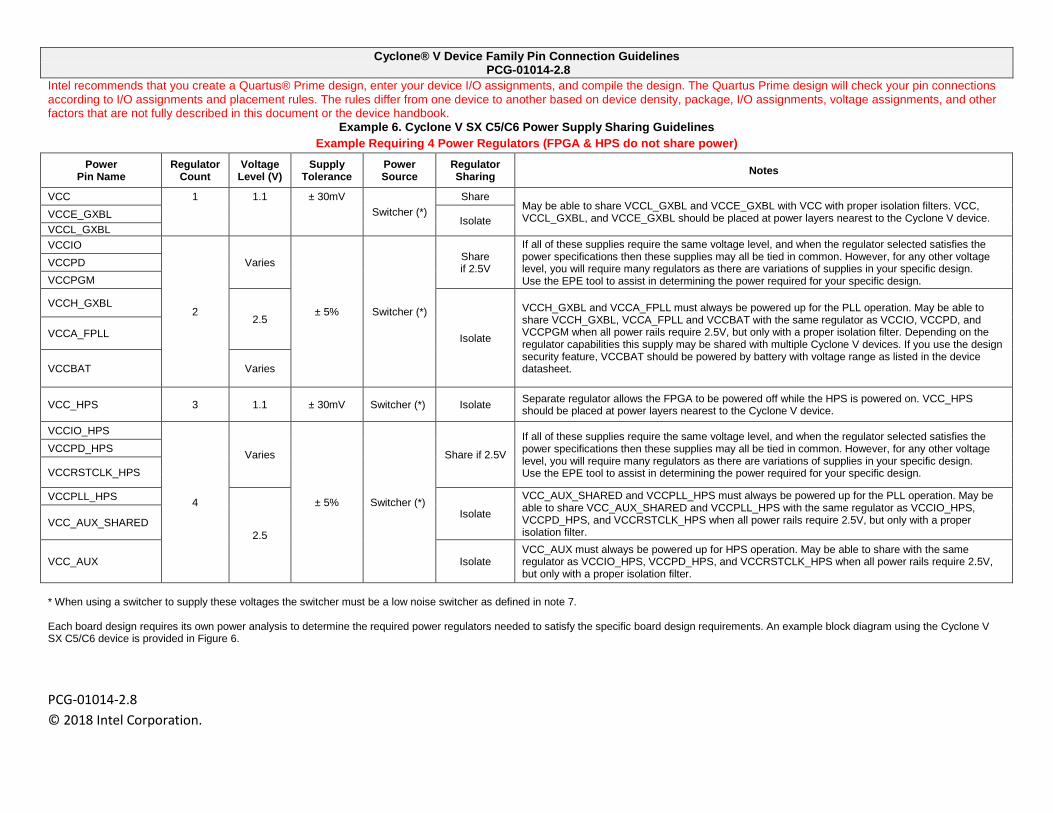
Cyclone® V Device Family Pin Connection Guidelines PCG-01014-2.8
Intel recommends that you create a Quartus® Prime design, enter your device I/O assignments, and compile the design. The Quartus Prime design will check your pin connections according to I/O assignments and placement rules. The rules differ from one device to another based on device density, package, I/O assignments, voltage assignments, and other factors that are not fully described in this document or the device handbook.
PCG-01014-2.8 © 2018 Intel Corporation.
Example 6. Cyclone V SX C5/C6 Power Supply Sharing Guidelines Example Requiring 4 Power Regulators (FPGA & HPS do not share power)
Power Pin Name
Regulator Count
Voltage Level (V)
Supply Tolerance
Power Source
Regulator Sharing Notes
VCC 1 1.1 ± 30mV Switcher (*)
Share May be able to share VCCL_GXBL and VCCE_GXBL with VCC with proper isolation filters. VCC, VCCL_GXBL, and VCCE_GXBL should be placed at power layers nearest to the Cyclone V device. VCCE_GXBL Isolate
VCCL_GXBL VCCIO
2
Varies
± 5% Switcher (*)
Share if 2.5V
If all of these supplies require the same voltage level, and when the regulator selected satisfies the power specifications then these supplies may all be tied in common. However, for any other voltage level, you will require many regulators as there are variations of supplies in your specific design. Use the EPE tool to assist in determining the power required for your specific design.
VCCPD VCCPGM
VCCH_GXBL 2.5
Isolate
VCCH_GXBL and VCCA_FPLL must always be powered up for the PLL operation. May be able to share VCCH_GXBL, VCCA_FPLL and VCCBAT with the same regulator as VCCIO, VCCPD, and VCCPGM when all power rails require 2.5V, but only with a proper isolation filter. Depending on the regulator capabilities this supply may be shared with multiple Cyclone V devices. If you use the design security feature, VCCBAT should be powered by battery with voltage range as listed in the device datasheet.
VCCA_FPLL
VCCBAT Varies
VCC_HPS 3 1.1 ± 30mV Switcher (*) Isolate Separate regulator allows the FPGA to be powered off while the HPS is powered on. VCC_HPS should be placed at power layers nearest to the Cyclone V device.
VCCIO_HPS
4
Varies
± 5% Switcher (*)
Share if 2.5V
If all of these supplies require the same voltage level, and when the regulator selected satisfies the power specifications then these supplies may all be tied in common. However, for any other voltage level, you will require many regulators as there are variations of supplies in your specific design. Use the EPE tool to assist in determining the power required for your specific design.
VCCPD_HPS
VCCRSTCLK_HPS
VCCPLL_HPS
2.5
Isolate
VCC_AUX_SHARED and VCCPLL_HPS must always be powered up for the PLL operation. May be able to share VCC_AUX_SHARED and VCCPLL_HPS with the same regulator as VCCIO_HPS, VCCPD_HPS, and VCCRSTCLK_HPS when all power rails require 2.5V, but only with a proper isolation filter.
VCC_AUX_SHARED
VCC_AUX Isolate VCC_AUX must always be powered up for HPS operation. May be able to share with the same regulator as VCCIO_HPS, VCCPD_HPS, and VCCRSTCLK_HPS when all power rails require 2.5V, but only with a proper isolation filter.
* When using a switcher to supply these voltages the switcher must be a low noise switcher as defined in note 7. Each board design requires its own power analysis to determine the required power regulators needed to satisfy the specific board design requirements. An example block diagram using the Cyclone V SX C5/C6 device is provided in Figure 6.
Cyclone® V Device Family Pin Connection Guidelines PCG-01014-2.8
Intel recommends that you create a Quartus® Prime design, enter your device I/O assignments, and compile the design. The Quartus Prime design will check your pin connections according to I/O assignments and placement rules. The rules differ from one device to another based on device density, package, I/O assignments, voltage assignments, and other factors that are not fully described in this document or the device handbook.
PCG-01014-2.8 © 2018 Intel Corporation.
Use the EPE (Early Power Estimation) tool to assist in determining the power required for your specific design. The Cyclone V performance is guaranteed with the recommended Enpirion power solutions. For a list of recommended Enpirion solutions for Cyclone V devices, refer to the PowerPlay Early Power Estimators (EPE) and Power Analyzer page. The recommended Enpirion solutions are included in the “Enpirion” tab of your completed EPE. For more details about the Enpirion power solutions, refer to the Enpirion Power page and the Powering FPGAs Resource Center. Refer to power up sequence recommendation in Cyclone V Devices Handbook: Power Managament in Cyclone V Devices.
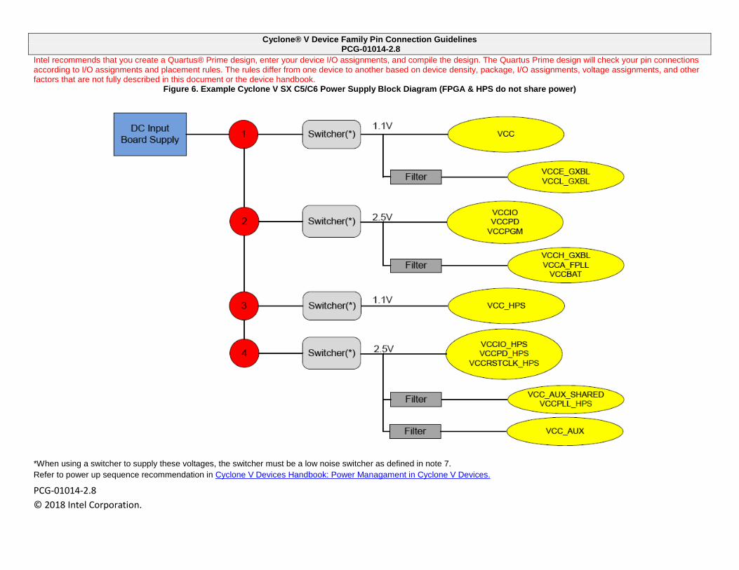
Cyclone® V Device Family Pin Connection Guidelines PCG-01014-2.8
Intel recommends that you create a Quartus® Prime design, enter your device I/O assignments, and compile the design. The Quartus Prime design will check your pin connections according to I/O assignments and placement rules. The rules differ from one device to another based on device density, package, I/O assignments, voltage assignments, and other factors that are not fully described in this document or the device handbook.
PCG-01014-2.8 © 2018 Intel Corporation.
Figure 6. Example Cyclone V SX C5/C6 Power Supply Block Diagram (FPGA & HPS do not share power)
*When using a switcher to supply these voltages, the switcher must be a low noise switcher as defined in note 7. Refer to power up sequence recommendation in Cyclone V Devices Handbook: Power Managament in Cyclone V Devices.
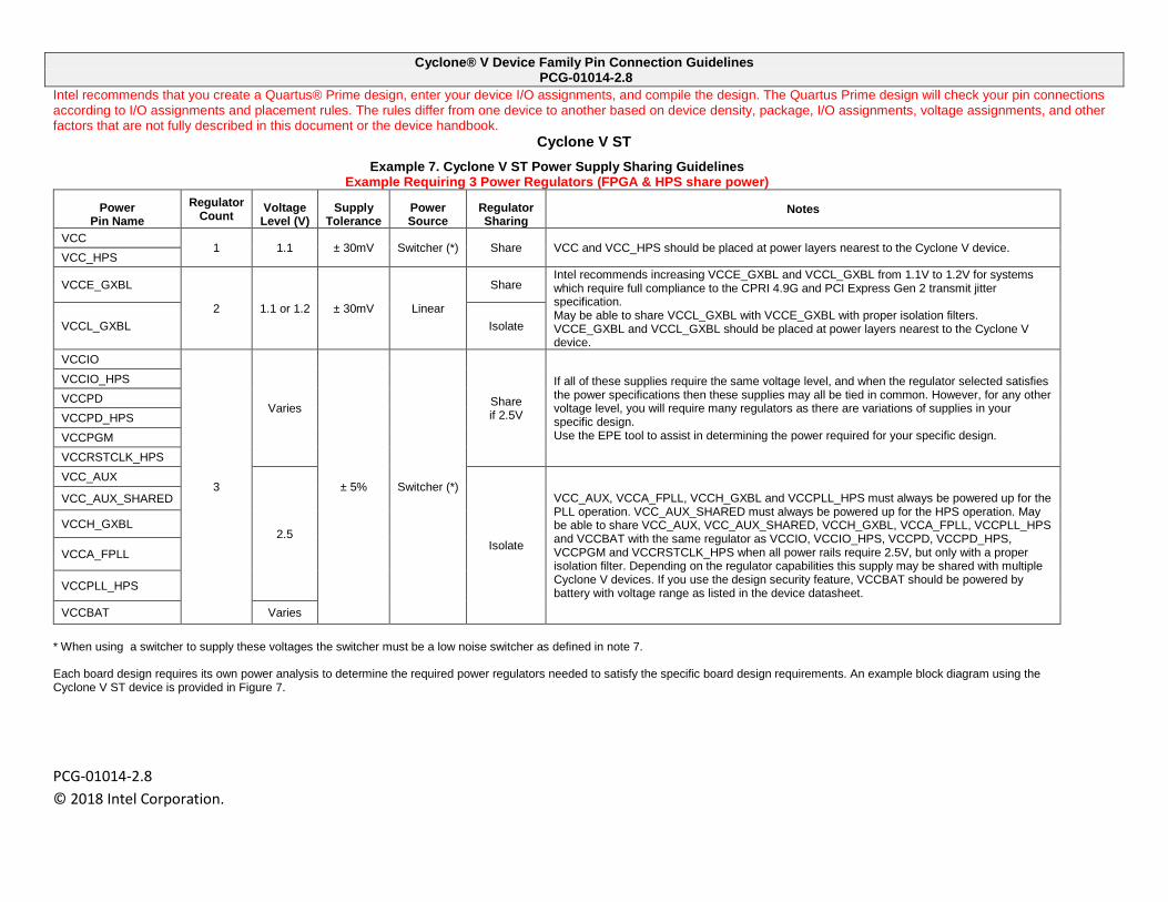
Cyclone® V Device Family Pin Connection Guidelines PCG-01014-2.8
Intel recommends that you create a Quartus® Prime design, enter your device I/O assignments, and compile the design. The Quartus Prime design will check your pin connections according to I/O assignments and placement rules. The rules differ from one device to another based on device density, package, I/O assignments, voltage assignments, and other factors that are not fully described in this document or the device handbook.
PCG-01014-2.8 © 2018 Intel Corporation.
Cyclone V ST Example 7. Cyclone V ST Power Supply Sharing Guidelines
Example Requiring 3 Power Regulators (FPGA & HPS share power)
Power Pin Name
Regulator Count Voltage
Level (V) Supply
Tolerance Power Source
Regulator Sharing
Notes
VCC 1 1.1 ± 30mV Switcher (*) Share VCC and VCC_HPS should be placed at power layers nearest to the Cyclone V device.
VCC_HPS
VCCE_GXBL
2 1.1 or 1.2 ± 30mV Linear
Share Intel recommends increasing VCCE_GXBL and VCCL_GXBL from 1.1V to 1.2V for systems which require full compliance to the CPRI 4.9G and PCI Express Gen 2 transmit jitter specification. May be able to share VCCL_GXBL with VCCE_GXBL with proper isolation filters. VCCE_GXBL and VCCL_GXBL should be placed at power layers nearest to the Cyclone V device.
VCCL_GXBL Isolate
VCCIO
3
Varies
± 5% Switcher (*)
Share if 2.5V
If all of these supplies require the same voltage level, and when the regulator selected satisfies the power specifications then these supplies may all be tied in common. However, for any other voltage level, you will require many regulators as there are variations of supplies in your specific design. Use the EPE tool to assist in determining the power required for your specific design.
VCCIO_HPS VCCPD VCCPD_HPS VCCPGM VCCRSTCLK_HPS VCC_AUX
2.5 Isolate
VCC_AUX, VCCA_FPLL, VCCH_GXBL and VCCPLL_HPS must always be powered up for the PLL operation. VCC_AUX_SHARED must always be powered up for the HPS operation. May be able to share VCC_AUX, VCC_AUX_SHARED, VCCH_GXBL, VCCA_FPLL, VCCPLL_HPS and VCCBAT with the same regulator as VCCIO, VCCIO_HPS, VCCPD, VCCPD_HPS, VCCPGM and VCCRSTCLK_HPS when all power rails require 2.5V, but only with a proper isolation filter. Depending on the regulator capabilities this supply may be shared with multiple Cyclone V devices. If you use the design security feature, VCCBAT should be powered by battery with voltage range as listed in the device datasheet.
VCC_AUX_SHARED
VCCH_GXBL
VCCA_FPLL
VCCPLL_HPS
VCCBAT Varies * When using a switcher to supply these voltages the switcher must be a low noise switcher as defined in note 7. Each board design requires its own power analysis to determine the required power regulators needed to satisfy the specific board design requirements. An example block diagram using the Cyclone V ST device is provided in Figure 7.
Cyclone® V Device Family Pin Connection Guidelines PCG-01014-2.8
Intel recommends that you create a Quartus® Prime design, enter your device I/O assignments, and compile the design. The Quartus Prime design will check your pin connections according to I/O assignments and placement rules. The rules differ from one device to another based on device density, package, I/O assignments, voltage assignments, and other factors that are not fully described in this document or the device handbook.
PCG-01014-2.8 © 2018 Intel Corporation.
Use the EPE (Early Power Estimation) tool to assist in determining the power required for your specific design. The Cyclone V performance is guaranteed with the recommended Enpirion power solutions. For a list of recommended Enpirion solutions for Cyclone V devices, refer to the PowerPlay Early Power Estimators (EPE) and Power Analyzer page. The recommended Enpirion solutions are included in the “Enpirion” tab of your completed EPE. For more details about the Enpirion power solutions, refer to the Enpirion Power page and the Powering FPGAs Resource Center. Refer to power up sequence recommendation in Cyclone V Devices Handbook: Power Managament in Cyclone V Devices.
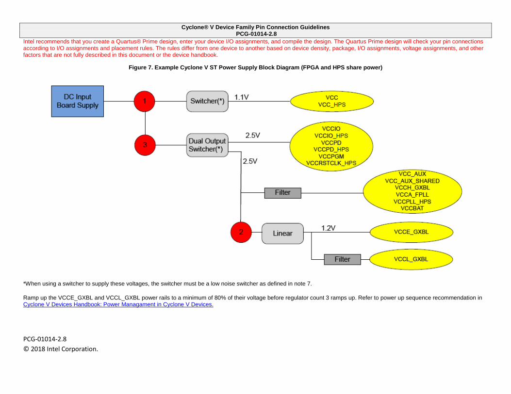
Cyclone® V Device Family Pin Connection Guidelines PCG-01014-2.8
Intel recommends that you create a Quartus® Prime design, enter your device I/O assignments, and compile the design. The Quartus Prime design will check your pin connections according to I/O assignments and placement rules. The rules differ from one device to another based on device density, package, I/O assignments, voltage assignments, and other factors that are not fully described in this document or the device handbook.
PCG-01014-2.8 © 2018 Intel Corporation.
Figure 7. Example Cyclone V ST Power Supply Block Diagram (FPGA and HPS share power)
*When using a switcher to supply these voltages, the switcher must be a low noise switcher as defined in note 7.
Ramp up the VCCE_GXBL and VCCL_GXBL power rails to a minimum of 80% of their voltage before regulator count 3 ramps up. Refer to power up sequence recommendation in Cyclone V Devices Handbook: Power Managament in Cyclone V Devices.
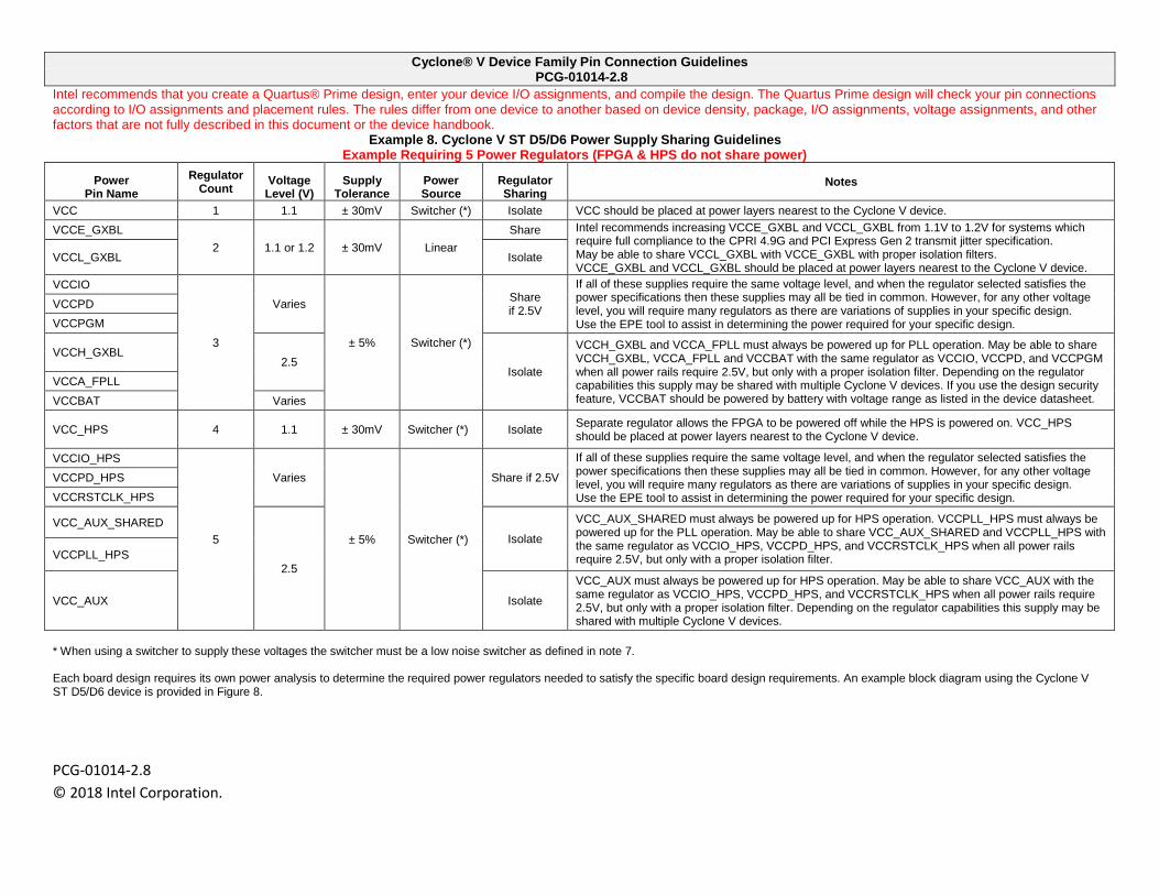
Cyclone® V Device Family Pin Connection Guidelines PCG-01014-2.8
Intel recommends that you create a Quartus® Prime design, enter your device I/O assignments, and compile the design. The Quartus Prime design will check your pin connections according to I/O assignments and placement rules. The rules differ from one device to another based on device density, package, I/O assignments, voltage assignments, and other factors that are not fully described in this document or the device handbook.
PCG-01014-2.8 © 2018 Intel Corporation.
Example 8. Cyclone V ST D5/D6 Power Supply Sharing Guidelines Example Requiring 5 Power Regulators (FPGA & HPS do not share power)
Power Pin Name
Regulator Count Voltage
Level (V) Supply
Tolerance Power Source
Regulator Sharing
Notes
VCC 1 1.1 ± 30mV Switcher (*) Isolate VCC should be placed at power layers nearest to the Cyclone V device. VCCE_GXBL
2 1.1 or 1.2 ± 30mV Linear Share Intel recommends increasing VCCE_GXBL and VCCL_GXBL from 1.1V to 1.2V for systems which
require full compliance to the CPRI 4.9G and PCI Express Gen 2 transmit jitter specification. May be able to share VCCL_GXBL with VCCE_GXBL with proper isolation filters. VCCE_GXBL and VCCL_GXBL should be placed at power layers nearest to the Cyclone V device.
VCCL_GXBL Isolate
VCCIO
3
Varies
± 5% Switcher (*)
Share if 2.5V
If all of these supplies require the same voltage level, and when the regulator selected satisfies the power specifications then these supplies may all be tied in common. However, for any other voltage level, you will require many regulators as there are variations of supplies in your specific design. Use the EPE tool to assist in determining the power required for your specific design.
VCCPD VCCPGM
VCCH_GXBL 2.5
Isolate
VCCH_GXBL and VCCA_FPLL must always be powered up for PLL operation. May be able to share VCCH_GXBL, VCCA_FPLL and VCCBAT with the same regulator as VCCIO, VCCPD, and VCCPGM when all power rails require 2.5V, but only with a proper isolation filter. Depending on the regulator capabilities this supply may be shared with multiple Cyclone V devices. If you use the design security feature, VCCBAT should be powered by battery with voltage range as listed in the device datasheet.
VCCA_FPLL VCCBAT Varies
VCC_HPS 4 1.1 ± 30mV Switcher (*) Isolate Separate regulator allows the FPGA to be powered off while the HPS is powered on. VCC_HPS should be placed at power layers nearest to the Cyclone V device.
VCCIO_HPS
5
Varies
± 5% Switcher (*)
Share if 2.5V
If all of these supplies require the same voltage level, and when the regulator selected satisfies the power specifications then these supplies may all be tied in common. However, for any other voltage level, you will require many regulators as there are variations of supplies in your specific design. Use the EPE tool to assist in determining the power required for your specific design.
VCCPD_HPS VCCRSTCLK_HPS
VCC_AUX_SHARED
2.5
Isolate
VCC_AUX_SHARED must always be powered up for HPS operation. VCCPLL_HPS must always be powered up for the PLL operation. May be able to share VCC_AUX_SHARED and VCCPLL_HPS with the same regulator as VCCIO_HPS, VCCPD_HPS, and VCCRSTCLK_HPS when all power rails require 2.5V, but only with a proper isolation filter. VCCPLL_HPS
VCC_AUX Isolate
VCC_AUX must always be powered up for HPS operation. May be able to share VCC_AUX with the same regulator as VCCIO_HPS, VCCPD_HPS, and VCCRSTCLK_HPS when all power rails require 2.5V, but only with a proper isolation filter. Depending on the regulator capabilities this supply may be shared with multiple Cyclone V devices.
* When using a switcher to supply these voltages the switcher must be a low noise switcher as defined in note 7. Each board design requires its own power analysis to determine the required power regulators needed to satisfy the specific board design requirements. An example block diagram using the Cyclone V ST D5/D6 device is provided in Figure 8.
Cyclone® V Device Family Pin Connection Guidelines PCG-01014-2.8
Intel recommends that you create a Quartus® Prime design, enter your device I/O assignments, and compile the design. The Quartus Prime design will check your pin connections according to I/O assignments and placement rules. The rules differ from one device to another based on device density, package, I/O assignments, voltage assignments, and other factors that are not fully described in this document or the device handbook.
PCG-01014-2.8 © 2018 Intel Corporation.
Use the EPE (Early Power Estimation) tool to assist in determining the power required for your specific design. The Cyclone V performance is guaranteed with the recommended Enpirion power solutions. For a list of recommended Enpirion solutions for Cyclone V devices, refer to the PowerPlay Early Power Estimators (EPE) and Power Analyzer page. The recommended Enpirion solutions are included in the “Enpirion” tab of your completed EPE. For more details about the Enpirion power solutions, refer to the Enpirion Power page and the Powering FPGAs Resource Center.
Refer to power up sequence recommendation in Cyclone V Devices Handbook: Power Managament in Cyclone V Devices.
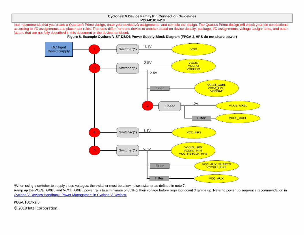
Cyclone® V Device Family Pin Connection Guidelines PCG-01014-2.8
Intel recommends that you create a Quartus® Prime design, enter your device I/O assignments, and compile the design. The Quartus Prime design will check your pin connections according to I/O assignments and placement rules. The rules differ from one device to another based on device density, package, I/O assignments, voltage assignments, and other factors that are not fully described in this document or the device handbook.
PCG-01014-2.8 © 2018 Intel Corporation.
Figure 8. Example Cyclone V ST D5/D6 Power Supply Block Diagram (FPGA & HPS do not share power)
*When using a switcher to supply these voltages, the switcher must be a low noise switcher as defined in note 7. Ramp up the VCCE_GXBL and VCCL_GXBL power rails to a minimum of 80% of their voltage before regulator count 3 ramps up. Refer to power up sequence recommendation in Cyclone V Devices Handbook: Power Managament in Cyclone V Devices.
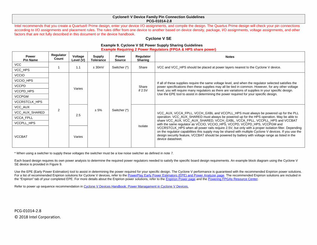
Cyclone® V Device Family Pin Connection Guidelines PCG-01014-2.8
Intel recommends that you create a Quartus® Prime design, enter your device I/O assignments, and compile the design. The Quartus Prime design will check your pin connections according to I/O assignments and placement rules. The rules differ from one device to another based on device density, package, I/O assignments, voltage assignments, and other factors that are not fully described in this document or the device handbook.
PCG-01014-2.8 © 2018 Intel Corporation.
Cyclone V SE Example 9. Cyclone V SE Power Supply Sharing Guidelines Example Requiring 2 Power Regulators (FPGA & HPS share power)
Power Pin Name
Regulator Count Voltage
Level (V) Supply
Tolerance Power Source
Regulator Sharing
Notes
VCC 1 1.1 ± 30mV Switcher (*) Share VCC and VCC_HPS should be placed at power layers nearest to the Cyclone V device.
VCC_HPS VCCIO
2
Varies
± 5% Switcher (*)
Share if 2.5V
If all of these supplies require the same voltage level, and when the regulator selected satisfies the power specifications then these supplies may all be tied in common. However, for any other voltage level, you will require many regulators as there are variations of supplies in your specific design. Use the EPE tool to assist in determining the power required for your specific design.
VCCIO_HPS VCCPD VCCPD_HPS VCCPGM VCCRSTCLK_HPS VCC_AUX
2.5
Isolate
VCC_AUX, VCCA_FPLL, VCCH_GXBL and VCCPLL_HPS must always be powered up for the PLL operation. VCC_AUX_SHARED must always be powered up for the HPS operation. May be able to share VCC_AUX, VCC_AUX_SHARED, VCCH_GXBL, VCCA_FPLL, VCCPLL_HPS and VCCBAT with the same regulator as VCCIO, VCCIO_HPS, VCCPD, VCCPD_HPS, VCCPGM and VCCRSTCLK_HPS when all power rails require 2.5V, but only with a proper isolation filter. Depending on the regulator capabilities this supply may be shared with multiple Cyclone V devices. If you use the design security feature, VCCBAT should be powered by battery with voltage range as listed in the device datasheet.
VCC_AUX_SHARED VCCA_FPLL VCCPLL_HPS
VCCBAT Varies
* When using a switcher to supply these voltages the switcher must be a low noise switcher as defined in note 7. Each board design requires its own power analysis to determine the required power regulators needed to satisfy the specific board design requirements. An example block diagram using the Cyclone V SE device is provided in Figure 9. Use the EPE (Early Power Estimation) tool to assist in determining the power required for your specific design. The Cyclone V performance is guaranteed with the recommended Enpirion power solutions. For a list of recommended Enpirion solutions for Cyclone V devices, refer to the PowerPlay Early Power Estimators (EPE) and Power Analyzer page. The recommended Enpirion solutions are included in the “Enpirion” tab of your completed EPE. For more details about the Enpirion power solutions, refer to the Enpirion Power page and the Powering FPGAs Resource Center. Refer to power up sequence recommendation in Cyclone V Devices Handbook: Power Managament in Cyclone V Devices.
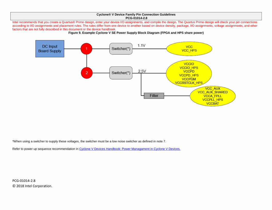
Cyclone® V Device Family Pin Connection Guidelines PCG-01014-2.8
Intel recommends that you create a Quartus® Prime design, enter your device I/O assignments, and compile the design. The Quartus Prime design will check your pin connections according to I/O assignments and placement rules. The rules differ from one device to another based on device density, package, I/O assignments, voltage assignments, and other factors that are not fully described in this document or the device handbook.
PCG-01014-2.8 © 2018 Intel Corporation.
Figure 9. Example Cyclone V SE Power Supply Block Diagram (FPGA and HPS share power)
*When using a switcher to supply these voltages, the switcher must be a low noise switcher as defined in note 7.
Refer to power up sequence recommendation in Cyclone V Devices Handbook: Power Managament in Cyclone V Devices.
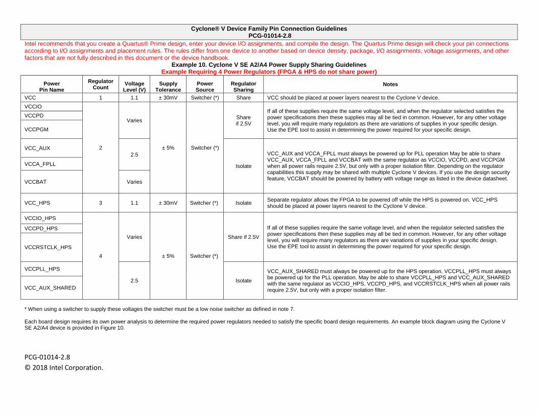
Cyclone® V Device Family Pin Connection Guidelines PCG-01014-2.8
Intel recommends that you create a Quartus® Prime design, enter your device I/O assignments, and compile the design. The Quartus Prime design will check your pin connections according to I/O assignments and placement rules. The rules differ from one device to another based on device density, package, I/O assignments, voltage assignments, and other factors that are not fully described in this document or the device handbook.
PCG-01014-2.8 © 2018 Intel Corporation.
Example 10. Cyclone V SE A2/A4 Power Supply Sharing Guidelines Example Requiring 4 Power Regulators (FPGA & HPS do not share power)
Power Pin Name
Regulator Count Voltage
Level (V) Supply
Tolerance Power Source
Regulator Sharing
Notes
VCC 1 1.1 ± 30mV Switcher (*) Share VCC should be placed at power layers nearest to the Cyclone V device. VCCIO
2
Varies
± 5% Switcher (*)
Share if 2.5V
If all of these supplies require the same voltage level, and when the regulator selected satisfies the power specifications then these supplies may all be tied in common. However, for any other voltage level, you will require many regulators as there are variations of supplies in your specific design. Use the EPE tool to assist in determining the power required for your specific design.
VCCPD
VCCPGM
VCC_AUX 2.5
Isolate
VCC_AUX and VCCA_FPLL must always be powered up for PLL operation May be able to share VCC_AUX, VCCA_FPLL and VCCBAT with the same regulator as VCCIO, VCCPD, and VCCPGM when all power rails require 2.5V, but only with a proper isolation filter. Depending on the regulator capabilities this supply may be shared with multiple Cyclone V devices. If you use the design security feature, VCCBAT should be powered by battery with voltage range as listed in the device datasheet.
VCCA_FPLL
VCCBAT Varies
VCC_HPS 3 1.1 ± 30mV Switcher (*) Isolate Separate regulator allows the FPGA to be powered off while the HPS is powered on. VCC_HPS should be placed at power layers nearest to the Cyclone V device.
VCCIO_HPS
4
Varies
± 5% Switcher (*)
Share if 2.5V
If all of these supplies require the same voltage level, and when the regulator selected satisfies the power specifications then these supplies may all be tied in common. However, for any other voltage level, you will require many regulators as there are variations of supplies in your specific design. Use the EPE tool to assist in determining the power required for your specific design.
VCCPD_HPS
VCCRSTCLK_HPS
VCCPLL_HPS
2.5 Isolate
VCC_AUX_SHARED must always be powered up for the HPS operation. VCCPLL_HPS must always be powered up for the PLL operation. May be able to share VCCPLL_HPS and VCC_AUX_SHARED with the same regulator as VCCIO_HPS, VCCPD_HPS, and VCCRSTCLK_HPS when all power rails require 2.5V, but only with a proper isolation filter. VCC_AUX_SHARED
* When using a switcher to supply these voltages the switcher must be a low noise switcher as defined in note 7. Each board design requires its own power analysis to determine the required power regulators needed to satisfy the specific board design requirements. An example block diagram using the Cyclone V SE A2/A4 device is provided in Figure 10.
Cyclone® V Device Family Pin Connection Guidelines PCG-01014-2.8
Intel recommends that you create a Quartus® Prime design, enter your device I/O assignments, and compile the design. The Quartus Prime design will check your pin connections according to I/O assignments and placement rules. The rules differ from one device to another based on device density, package, I/O assignments, voltage assignments, and other factors that are not fully described in this document or the device handbook.
PCG-01014-2.8 © 2018 Intel Corporation.
Use the EPE (Early Power Estimation) tool to assist in determining the power required for your specific design. The Cyclone V performance is guaranteed with the recommended Enpirion power solutions. For a list of recommended Enpirion solutions for Cyclone V devices, refer to the PowerPlay Early Power Estimators (EPE) and Power Analyzer page. The recommended Enpirion solutions are included in the “Enpirion” tab of your completed EPE. For more details about the Enpirion power solutions, refer to the Enpirion Power page and the Powering FPGAs Resource Center.
Refer to power up sequence recommendation in Cyclone V Devices Handbook: Power Managament in Cyclone V Devices.
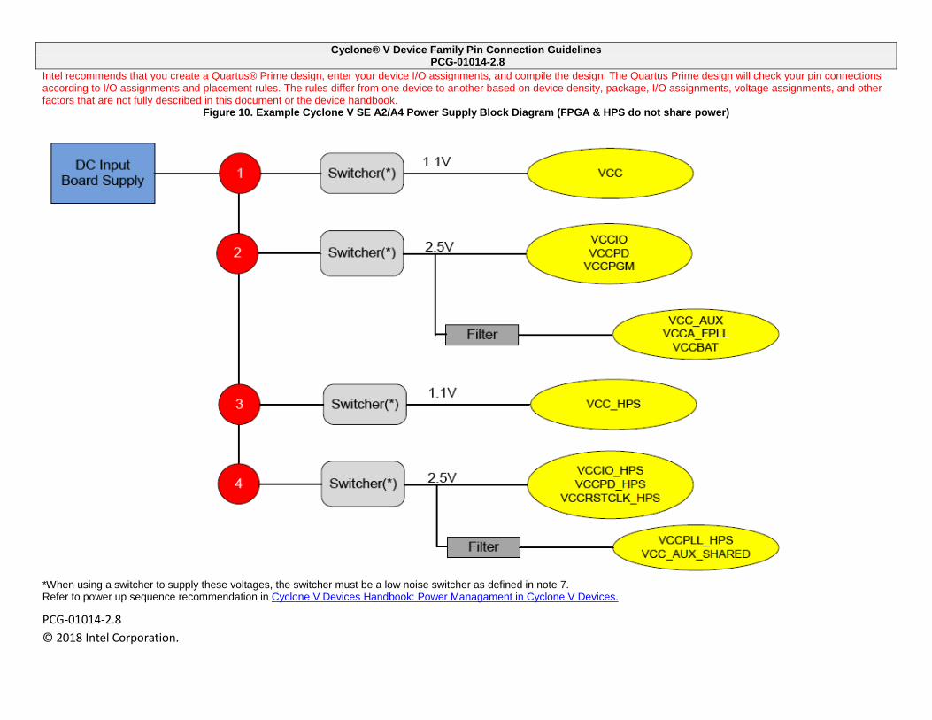
Cyclone® V Device Family Pin Connection Guidelines PCG-01014-2.8
Intel recommends that you create a Quartus® Prime design, enter your device I/O assignments, and compile the design. The Quartus Prime design will check your pin connections according to I/O assignments and placement rules. The rules differ from one device to another based on device density, package, I/O assignments, voltage assignments, and other factors that are not fully described in this document or the device handbook.
PCG-01014-2.8 © 2018 Intel Corporation.
Figure 10. Example Cyclone V SE A2/A4 Power Supply Block Diagram (FPGA & HPS do not share power)
*When using a switcher to supply these voltages, the switcher must be a low noise switcher as defined in note 7. Refer to power up sequence recommendation in Cyclone V Devices Handbook: Power Managament in Cyclone V Devices.
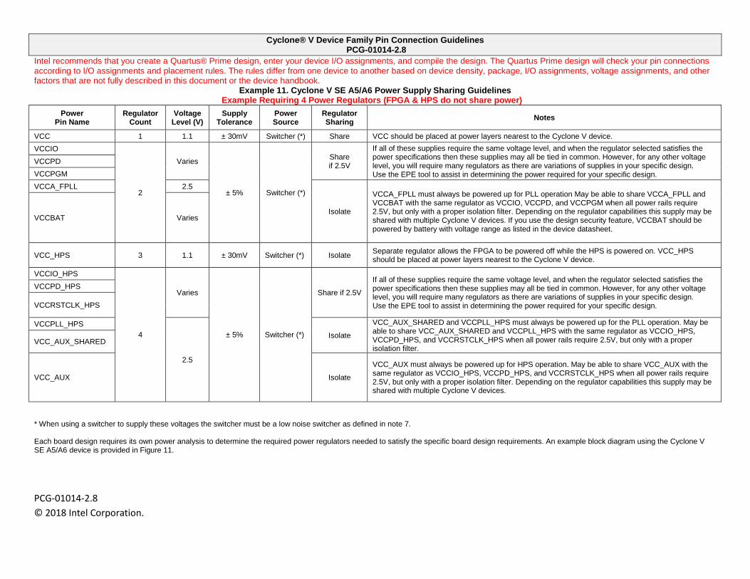
Cyclone® V Device Family Pin Connection Guidelines PCG-01014-2.8
Intel recommends that you create a Quartus® Prime design, enter your device I/O assignments, and compile the design. The Quartus Prime design will check your pin connections according to I/O assignments and placement rules. The rules differ from one device to another based on device density, package, I/O assignments, voltage assignments, and other factors that are not fully described in this document or the device handbook.
PCG-01014-2.8 © 2018 Intel Corporation.
Example 11. Cyclone V SE A5/A6 Power Supply Sharing Guidelines Example Requiring 4 Power Regulators (FPGA & HPS do not share power)
Power Pin Name
Regulator Count
Voltage Level (V)
Supply Tolerance
Power Source
Regulator Sharing Notes
VCC 1 1.1 ± 30mV Switcher (*) Share VCC should be placed at power layers nearest to the Cyclone V device. VCCIO
2
Varies
± 5% Switcher (*)
Share if 2.5V
If all of these supplies require the same voltage level, and when the regulator selected satisfies the power specifications then these supplies may all be tied in common. However, for any other voltage level, you will require many regulators as there are variations of supplies in your specific design. Use the EPE tool to assist in determining the power required for your specific design.
VCCPD VCCPGM VCCA_FPLL 2.5
Isolate
VCCA_FPLL must always be powered up for PLL operation May be able to share VCCA_FPLL and VCCBAT with the same regulator as VCCIO, VCCPD, and VCCPGM when all power rails require 2.5V, but only with a proper isolation filter. Depending on the regulator capabilities this supply may be shared with multiple Cyclone V devices. If you use the design security feature, VCCBAT should be powered by battery with voltage range as listed in the device datasheet.
VCCBAT Varies
VCC_HPS 3 1.1 ± 30mV Switcher (*) Isolate Separate regulator allows the FPGA to be powered off while the HPS is powered on. VCC_HPS should be placed at power layers nearest to the Cyclone V device.
VCCIO_HPS
4
Varies
± 5% Switcher (*)
Share if 2.5V
If all of these supplies require the same voltage level, and when the regulator selected satisfies the power specifications then these supplies may all be tied in common. However, for any other voltage level, you will require many regulators as there are variations of supplies in your specific design. Use the EPE tool to assist in determining the power required for your specific design.
VCCPD_HPS
VCCRSTCLK_HPS
VCCPLL_HPS
2.5
Isolate
VCC_AUX_SHARED and VCCPLL_HPS must always be powered up for the PLL operation. May be able to share VCC_AUX_SHARED and VCCPLL_HPS with the same regulator as VCCIO_HPS, VCCPD_HPS, and VCCRSTCLK_HPS when all power rails require 2.5V, but only with a proper isolation filter.
VCC_AUX_SHARED
VCC_AUX Isolate
VCC_AUX must always be powered up for HPS operation. May be able to share VCC_AUX with the same regulator as VCCIO_HPS, VCCPD_HPS, and VCCRSTCLK_HPS when all power rails require 2.5V, but only with a proper isolation filter. Depending on the regulator capabilities this supply may be shared with multiple Cyclone V devices.
* When using a switcher to supply these voltages the switcher must be a low noise switcher as defined in note 7. Each board design requires its own power analysis to determine the required power regulators needed to satisfy the specific board design requirements. An example block diagram using the Cyclone V SE A5/A6 device is provided in Figure 11.

Cyclone® V Device Family Pin Connection Guidelines PCG-01014-2.8
Intel recommends that you create a Quartus® Prime design, enter your device I/O assignments, and compile the design. The Quartus Prime design will check your pin connections according to I/O assignments and placement rules. The rules differ from one device to another based on device density, package, I/O assignments, voltage assignments, and other factors that are not fully described in this document or the device handbook.
PCG-01014-2.8 © 2018 Intel Corporation.
Use the EPE (Early Power Estimation) tool to assist in determining the power required for your specific design. The Cyclone V performance is guaranteed with the recommended Enpirion power solutions. For a list of recommended Enpirion solutions for Cyclone V devices, refer to the PowerPlay Early Power Estimators (EPE) and Power Analyzer page. The recommended Enpirion solutions are included in the “Enpirion” tab of your completed EPE. For more details about the Enpirion power solutions, refer to the Enpirion Power page and the Powering FPGAs Resource Center.
Refer to power up sequence recommendation in Cyclone V Devices Handbook: Power Managament in Cyclone V Devices.
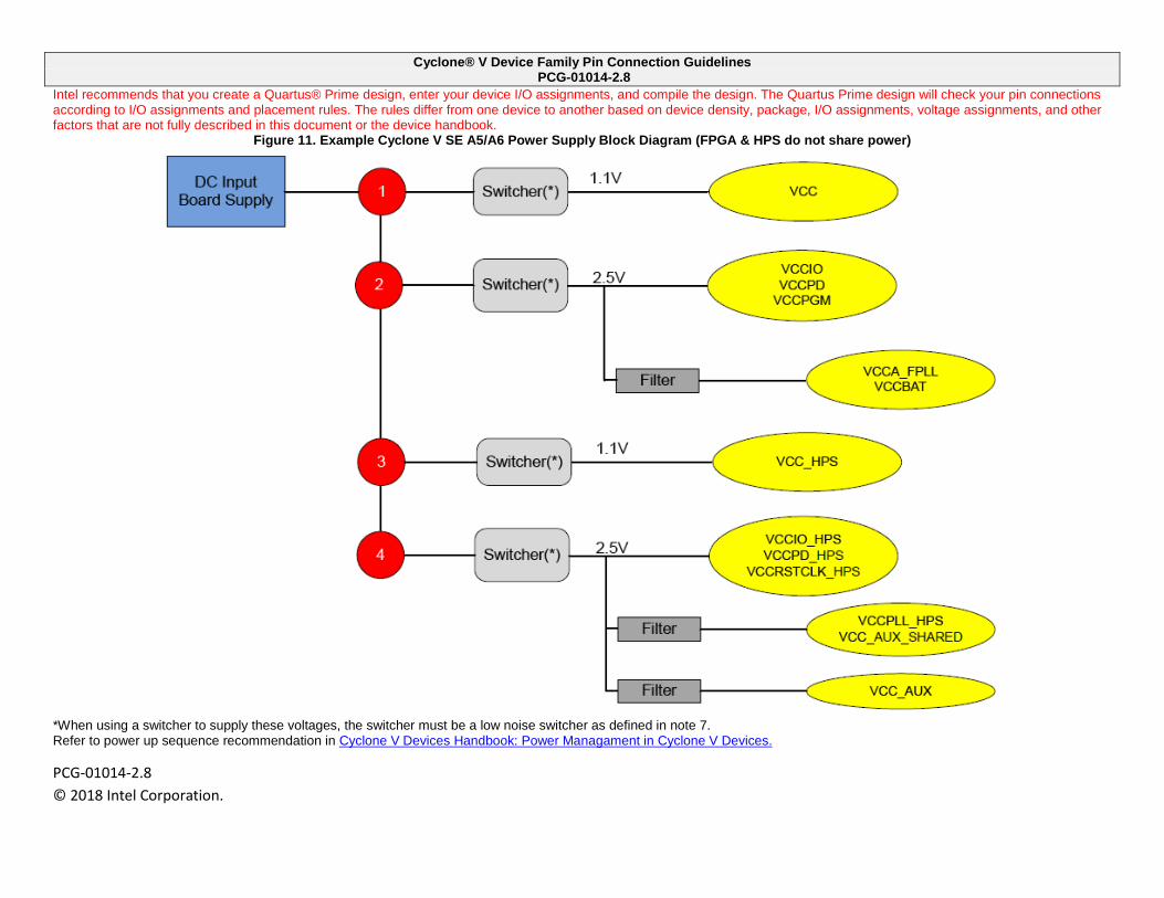
Cyclone® V Device Family Pin Connection Guidelines PCG-01014-2.8
Intel recommends that you create a Quartus® Prime design, enter your device I/O assignments, and compile the design. The Quartus Prime design will check your pin connections according to I/O assignments and placement rules. The rules differ from one device to another based on device density, package, I/O assignments, voltage assignments, and other factors that are not fully described in this document or the device handbook.
PCG-01014-2.8 © 2018 Intel Corporation.
Figure 11. Example Cyclone V SE A5/A6 Power Supply Block Diagram (FPGA & HPS do not share power)
*When using a switcher to supply these voltages, the switcher must be a low noise switcher as defined in note 7. Refer to power up sequence recommendation in Cyclone V Devices Handbook: Power Managament in Cyclone V Devices.
Cyclone® V Device Family Pin Connection Guidelines PCG-01014-2.8
Intel recommends that you create a Quartus® Prime design, enter your device I/O assignments, and compile the design. The Quartus Prime design will check your pin connections according to I/O assignments and placement rules. The rules differ from one device to another based on device density, package, I/O assignments, voltage assignments, and other factors that are not fully described in this document or the device handbook.
PCG-01014-2.8 © 2018 Intel Corporation.
Revision History Revision Description of Changes Date
1.0 Initial Release. 11/25/2011 1.1 Updated VCCA_FPLL and VCCH_GXBL power-up requirements. 3/29/2012 1.2 Added power supply sharing guidelines for Cyclone V GT and E devices, updated the pull-down requirement for unused transceiver receivers and
REFCLK pins, and updated the INIT_DONE pin connection guidelines. 6/13/2012
1.3 Updated the power sharing guidelines for Cyclone V GT devices and updated the VCCE_GXBL, VCCL_GXBL, and nPERST[L0,L1] connection guidelines.
10/16/2012
1.4 • Added HPS Pin Connection Guidelines. • Added power supply sharing guidelines for Cyclone V SX, ST, and SE devices. • Added [B,T]_DQS_[#], [B,T]_DQS#_[#], and [B,T]_DQ_[#] pins. • Updated pin description and connection guidelines for the VREF pin. • Updated connection guidelines for the RREF pin. • Updated pin description for the DIFFIO_TX pin.
11/19/2012
1.5 • Updated Connection Guidelines for HPS_CLK1 and HPS_CLK2 with 'VCCRSTCLK_HPS'. • Updated Pin Description for DIFFIO_TX_[B,T,R][#:#]p, DIFFIO_TX_[B,T,R][#:#]n with 'transmitter'. • Updated Connection Guidelines where 'If powering down the FPGA fabric is required, tie this pin to 2.5V' is removed and "See Notes 2,3,4, and
7." is added • Updated Pin Description for NAND_DQ0, NAND_DQ3 and NAND_DQ5 with 'Receive'. • Updated Pin Description for TRACE_D3 with 'Slave'. • Updated Note 7) with 'The switching frequency range is not an Altera requirement. However, Altera does require the Line Regulation and Load
Regulation meet the following specifications:' • Added VREFB[#]N0_HPS pin.
1/22/2013
1.6 • Updated Connection Guidelines for VCC_AUX. • Updated Connection Guidlines for VCC_AUX_SHARED. • Updated Connection Guidelines for HPS_GPI#. • Added power diagrams for Cyclone SX/ST/SE devices supporting FPGA split power. • Added BSEL and CSEL mnemonics to HPS Boot Select and Clock Select signals • Updated BSEL and CSEL as primary function. • Added the exception that GXB_REFCLK can be DC coupled for the single case of the PCIe HCSL I/O standard. • Updated Connection Guidelines for HPS_CLK2. • Updated Connection Guidelines for RREF_TL for consistency. • Updated Connection Guidelines for VCCIO[#]_HPS by removing 1.25V and 1.35V support. • Updated Pin Description for VCCIO[#]_HPS by removing 135, 125. • Added Notes 12. and 13. for Differential I/O pins. • Updated Connection Guidelines for CLKUSR and RZQ. • Added CPRI 6.144G and link to transceiver chapters and datasheet for VCCE_GXBL and VCCL_GXBL. • Added Example 5, Figure 5, Example 6, Figure 6, Example 8, Figure 8, Example 10, Figure 10, Example 11 and Figure 11.
5/15/2013
1.7 Updated Connection Guidelines for REFCLK. 5/17/2013 1.8 Updated Note 13. with the restriction guidelines that are applicable for the Cyclone V LVDS transmitters. 9/4/2013 1.9 • Updated Connection Guidelines for TMS, HPS_TMS, TDI, HPS_TDI, TDO, HPS_TDO, nPERST, VCCIO_HPS, SDMMC_CMD, and
SDMMC_D0. 10/9/2013
Cyclone® V Device Family Pin Connection Guidelines PCG-01014-2.8
Intel recommends that you create a Quartus® Prime design, enter your device I/O assignments, and compile the design. The Quartus Prime design will check your pin connections according to I/O assignments and placement rules. The rules differ from one device to another based on device density, package, I/O assignments, voltage assignments, and other factors that are not fully described in this document or the device handbook.
PCG-01014-2.8 © 2018 Intel Corporation.
• Updated Note (10) for both Pin Connection Guidelines and HPS Pin Connection Guidelines. 2.0 • Updated Pin Description for RREF_TL.
• Updated Connection Guidelines for VCCBAT. • Removed notes 11, 12 and 13 I/O rules for DIFFIO_TX, DIFFIO_RX and DIFFOUT pins. • Added KDB reference to DIFFIO_TX, DIFFIO_RX and DIFFOUT pins guidelines. • Added note to VREFB[#]N0_HPS. • Add note to power supply sharing guidelines for Enpirion solutions. • Changed pull-down resistor values for BSEL/CSEL pins to 1K ohm. • Changed figure 2, 7 and 8.
12/15/2014
2.1 • Added links referring to Cyclone V Device Handbook: Power Management in Cyclone V Devices for all power sharing guidelines tables and figures.
• Updated content in the Disclaimer section. • Added Note 13 for HPS Peripheral Pins and General Purpose Input Pins.
6/5/2015
2.2 • Added a note (14) to HPS peripheral pins that uses USB0 interface. 10/8/2015 2.3 • Clarified that Cyclone V E and SE devices do not have Hard IP for PCI Express instances and nPERSTL pins. 12/17/2015 2.4 • Changed nCSO/DATA4 pin type from output to bidirectional 4/14/2016 2.5 • Removed SDMMC_FB_CLK_IN pin.
• Added HPS_GPIO44 pin as General Purpose I/O bit 44. • Removed 1.2 LVTTL/LVCMOS and HSTL 12 support for VCCIO[#]_HPS pin.
10/28/2016
2.6 • Changed 10-kW to 10-kΩ for CRC_ERROR pin. 2/2/2017 2.7 • Added a note (15) to SDMMC_D3 pin.
• Added guideline to pull-up SDMMC_D1, SDMMC_D2, SDMMC_D3, SDMMC_D4, SDMMC_D5, SDMMC_D6, and SDMMC_D7 pins when booting HPS from an MMC/eMMC device.
• Added guideline for shared VCCPD pins across I/O banks.
11/17/2017
2.8 • Removed note “During JTAG programming, the nCONFIG status is ignored” for nCONFIG pin. 4/20/2018