PCF8579 LCD column driver for dot matrix graphic displays · 1. General description The PCF8579 is...
41
1. General description The PCF8579 is a low power CMOS 1 LCD column driver, designed to drive dot matrix graphic displays at multiplex rates of 1:8, 1:16, 1:24 or 1:32. The device has 40 outputs and can drive 32 × 40 dots in a 32 row multiplexed LCD. Up to 16 PCF8579s can be cascaded and up to 32 devices may be used on the same I 2 C-bus (using the two slave addresses). The device is optimized for use with the PCF8578 LCD row/column driver. Together these devices form a general purpose LCD dot matrix driver chip set, capable of driving displays of up to 40960 dots. The PCF8579 is compatible with most microcontrollers and communicates via a two-line bidirectional bus (I 2 C-bus). To allow partial V DD shutdown the ESD protection system of the SCL and SDA pins does not use a diode connected to V DD . Communication overhead is minimized by a display RAM with auto-incremented addressing and display bank switching. 2. Features ■ LCD column driver ■ Used in conjunction with the PCF8578, this device forms part of a chip set capable of driving up to 40960 dots ■ 40 column outputs ■ Selectable multiplex rates; 1:8, 1:16, 1:24 or 1:32 ■ Externally selectable bias configuration, 5 or 6 levels ■ Easily cascadable for large applications (up to 32 devices) ■ 1280-bit RAM for display data storage ■ Display memory bank switching ■ Auto-incremented data loading across hardware subaddress boundaries (with PCF8578) ■ Power-On Reset (POR) blanks display ■ Logic voltage supply range 2.5 V to 6 V ■ Maximum LCD supply voltage 9 V ■ Low power consumption ■ I 2 C-bus interface ■ Compatible with most microcontrollers ■ Optimized pinning for single plane wiring in multiple device applications (with PCF8578) ■ Space saving 56-lead small outline package and 64-pin quad flat pack PCF8579 LCD column driver for dot matrix graphic displays Rev. 05 — 11 May 2009 Product data sheet 1. The definition of the abbreviations and acronyms used in this data sheet can be found in Section 15.
Transcript of PCF8579 LCD column driver for dot matrix graphic displays · 1. General description The PCF8579 is...
1. General description
The PCF8579 is a low power CMOS1 LCD column driver, designed to drive dot matrixgraphic displays at multiplex rates of 1:8, 1:16, 1:24 or 1:32. The device has 40 outputsand can drive 32 × 40 dots in a 32 row multiplexed LCD. Up to 16 PCF8579s can becascaded and up to 32 devices may be used on the same I2C-bus (using the two slaveaddresses). The device is optimized for use with the PCF8578 LCD row/column driver.Together these devices form a general purpose LCD dot matrix driver chip set, capable ofdriving displays of up to 40960 dots. The PCF8579 is compatible with mostmicrocontrollers and communicates via a two-line bidirectional bus (I2C-bus). To allowpartial VDD shutdown the ESD protection system of the SCL and SDA pins does not use adiode connected to VDD. Communication overhead is minimized by a display RAM withauto-incremented addressing and display bank switching.
2. Features
n LCD column driver
n Used in conjunction with the PCF8578, this device forms part of a chip set capable ofdriving up to 40960 dots
n 40 column outputs
n Selectable multiplex rates; 1:8, 1:16, 1:24 or 1:32
n Externally selectable bias configuration, 5 or 6 levels
n Easily cascadable for large applications (up to 32 devices)
n 1280-bit RAM for display data storage
n Display memory bank switching
n Auto-incremented data loading across hardware subaddress boundaries (withPCF8578)
n Power-On Reset (POR) blanks display
n Logic voltage supply range 2.5 V to 6 V
n Maximum LCD supply voltage 9 V
n Low power consumption
n I2C-bus interface
n Compatible with most microcontrollers
n Optimized pinning for single plane wiring in multiple device applications (withPCF8578)
n Space saving 56-lead small outline package and 64-pin quad flat pack
PCF8579LCD column driver for dot matrix graphic displaysRev. 05 — 11 May 2009 Product data sheet
1. The definition of the abbreviations and acronyms used in this data sheet can be found in Section 15.
NXP Semiconductors PCF8579LCD column driver for dot matrix graphic displays
3. Applications
n Automotive information systems
n Telecommunication systems
n Point-of-sale terminals
n Industrial computer terminals
n Instrumentation
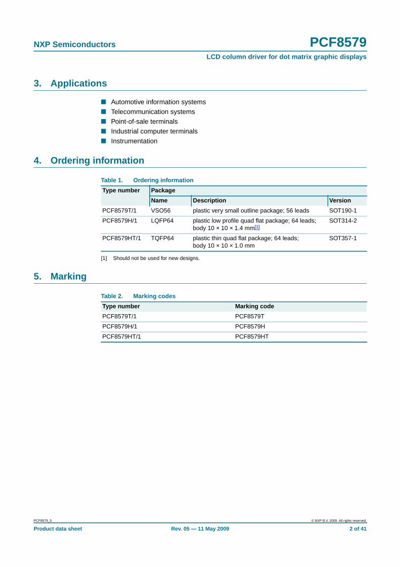
4. Ordering information
[1] Should not be used for new designs.
5. Marking
Table 1. Ordering information
Type number Package
Name Description Version
PCF8579T/1 VSO56 plastic very small outline package; 56 leads SOT190-1
PCF8579H/1 LQFP64 plastic low profile quad flat package; 64 leads;body 10 × 10 × 1.4 mm[1]
SOT314-2
PCF8579HT/1 TQFP64 plastic thin quad flat package; 64 leads;body 10 × 10 × 1.0 mm
SOT357-1
Table 2. Marking codes
Type number Marking code
PCF8579T/1 PCF8579T
PCF8579H/1 PCF8579H
PCF8579HT/1 PCF8579HT
PCF8579_5 © NXP B.V. 2009. All rights reserved.
Product data sheet Rev. 05 — 11 May 2009 2 of 41
NXP Semiconductors PCF8579LCD column driver for dot matrix graphic displays
6. Block diagram
(1) Operates at LCD voltage levels, all other blocks operate at logic levels.
Fig 1. Block diagram
C39 - C0
msa919
VDD
PCF8579
VLCD
V3
V4
OUTPUTCONTROLLER
COLUMN(1)
DRIVERS
Y DECODERAND SENSING
AMPLIFIERS
32 × 40 BITDISPLAY RAM
X DECODER
DISPLAYDECODER
RAM DATA POINTERSUBADDRESSCOUNTER
TIMINGGENERATOR
I2C-BUSCONTROLLER
INPUTFILTERS
COMMANDDECODER
POWER-ONRESET
TEST
SCL
SDA
n.c. SA0
CLK
SYNC
Y X
A3A2A1A0
VSS
PCF8579_5 © NXP B.V. 2009. All rights reserved.
Product data sheet Rev. 05 — 11 May 2009 3 of 41
NXP Semiconductors PCF8579LCD column driver for dot matrix graphic displays
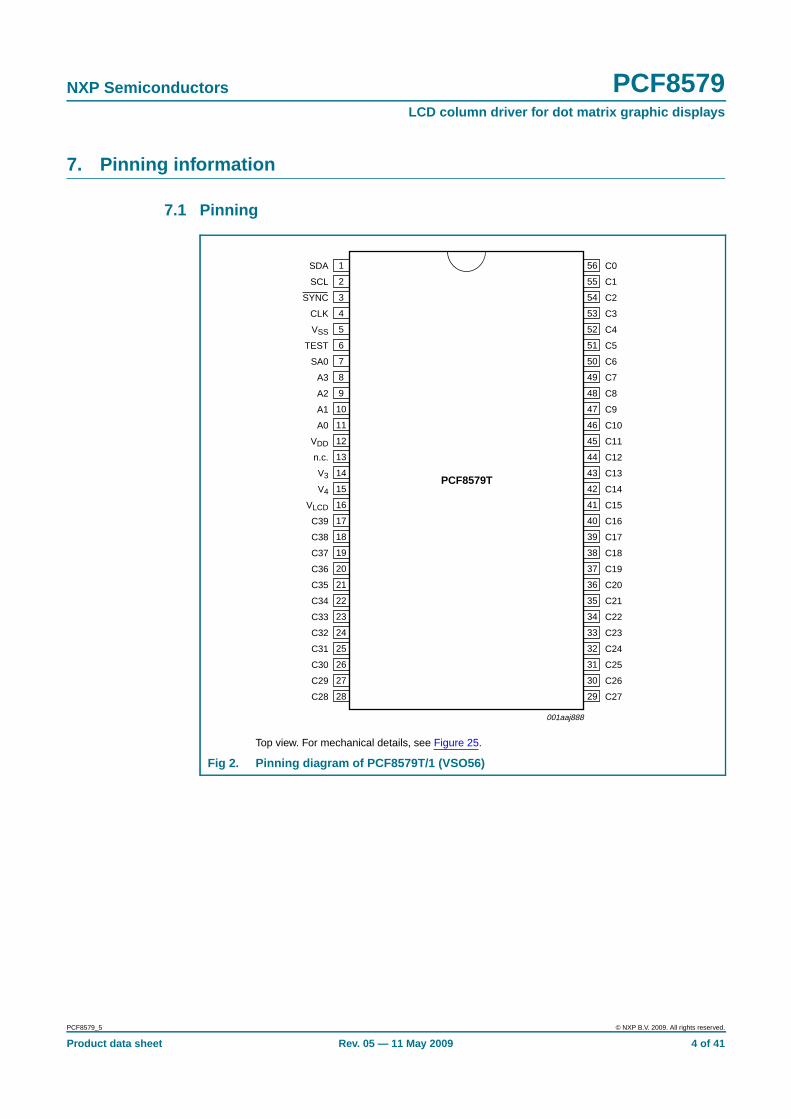
7. Pinning information
7.1 Pinning
Top view. For mechanical details, see Figure 25.
Fig 2. Pinning diagram of PCF8579T/1 (VSO56)
PCF8579T
SDA C0
SCL C1
SYNC C2
CLK C3
VSS C4
TEST C5
SA0 C6
A3 C7
A2 C8
A1 C9
A0 C10
VDD C11
n.c. C12
V3 C13
V4 C14
VLCD C15
C39 C16
C38 C17
C37 C18
C36 C19
C35 C20
C34 C21
C33 C22
C32 C23
C31 C24
C30 C25
C29 C26
C28 C27
001aaj888
1
2
3
4
5
6
7
8
9
10
11
12
13
14
15
16
17
18
19
20
21
22
23
24
25
26
27
28
56
55
54
53
52
51
50
49
48
47
46
45
44
43
42
41
40
39
38
37
36
35
34
33
32
31
30
29
PCF8579_5 © NXP B.V. 2009. All rights reserved.
Product data sheet Rev. 05 — 11 May 2009 4 of 41

NXP Semiconductors PCF8579LCD column driver for dot matrix graphic displays
Top view. For mechanical details, see Figure 26.
Fig 3. Pinning diagram of PCF8579H/1 (LQFP64)
PCF8579H
C5 C22
C4 C23
C3 C24
C2 C25
C1 C26
C0 C27
SDA C28
SCL C29
SYNC C30
CLK C31
VSS C32
TEST C33
SA0 C34
A3 C35
n.c. n.c.
A2 C36
A1
C6
A0
C7
n.c.
C8
VD
DC
9
n.c.
C10
V3
C11
V4
C12
VLC
DC
13
n.c.
C14
n.c.
C15
n.c.
C16
n.c.
C17
n.c.
C18
C39
C19
C38
C20
C37
C21
001aaj954
1
2
3
4
5
6
7
8
9
10
11
12
13
14
15
16
48
47
46
45
44
43
42
41
40
39
38
37
36
35
34
33
17 18 19 20 21 22 23 24 25 26 27 28 29 30 31 32
64 63 62 61 60 59 58 57 56 55 54 53 52 51 50 49
PCF8579_5 © NXP B.V. 2009. All rights reserved.
Product data sheet Rev. 05 — 11 May 2009 5 of 41
NXP Semiconductors PCF8579LCD column driver for dot matrix graphic displays
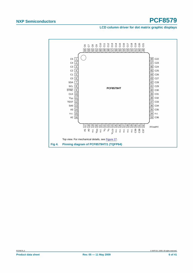
Top view. For mechanical details, see Figure 27.
Fig 4. Pinning diagram of PCF8579HT/1 (TQFP64)
PCF8579HT
C5 C22
C4 C23
C3 C24
C2 C25
C1 C26
C0 C27
SDA C28
SCL C29
SYNC C30
CLK C31
VSS C32
TEST C33
SA0 C34
A3 C35
n.c. n.c.
A2 C36
A1
C6
A0
C7
n.c.
C8
VD
DC
9
n.c.
C10
V3
C11
V4
C12
VLC
DC
13
n.c.
C14
n.c.
C15
n.c.
C16
n.c.
C17
n.c.
C18
C39
C19
C38
C20
C37
C21
001aaj841
1
2
3
4
5
6
7
8
9
10
11
12
13
14
15
16
48
47
46
45
44
43
42
41
40
39
38
37
36
35
34
33
17 18 19 20 21 22 23 24 25 26 27 28 29 30 31 32
64 63 62 61 60 59 58 57 56 55 54 53 52 51 50 49
PCF8579_5 © NXP B.V. 2009. All rights reserved.
Product data sheet Rev. 05 — 11 May 2009 6 of 41
NXP Semiconductors PCF8579LCD column driver for dot matrix graphic displays
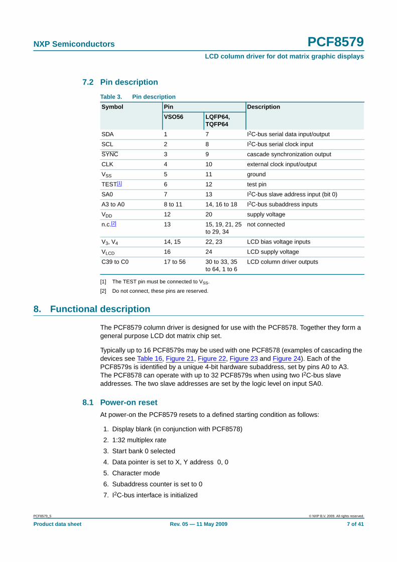
7.2 Pin description
[1] The TEST pin must be connected to VSS.
[2] Do not connect, these pins are reserved.
8. Functional description
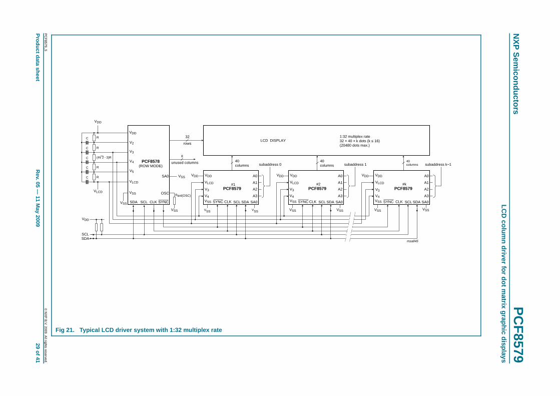
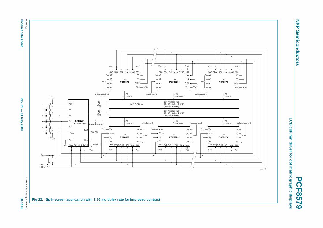
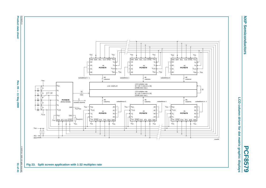
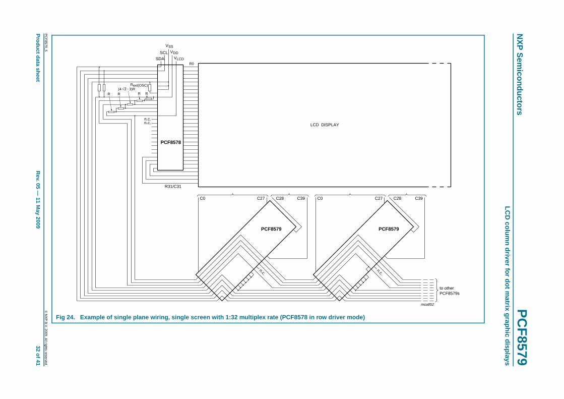
The PCF8579 column driver is designed for use with the PCF8578. Together they form ageneral purpose LCD dot matrix chip set.
Typically up to 16 PCF8579s may be used with one PCF8578 (examples of cascading thedevices see Table 16, Figure 21, Figure 22, Figure 23 and Figure 24). Each of thePCF8579s is identified by a unique 4-bit hardware subaddress, set by pins A0 to A3.The PCF8578 can operate with up to 32 PCF8579s when using two I2C-bus slaveaddresses. The two slave addresses are set by the logic level on input SA0.
8.1 Power-on resetAt power-on the PCF8579 resets to a defined starting condition as follows:
1. Display blank (in conjunction with PCF8578)
2. 1:32 multiplex rate
3. Start bank 0 selected
4. Data pointer is set to X, Y address 0, 0
5. Character mode
6. Subaddress counter is set to 0
7. I2C-bus interface is initialized
Table 3. Pin description
Symbol Pin Description
VSO56 LQFP64,TQFP64
SDA 1 7 I2C-bus serial data input/output
SCL 2 8 I2C-bus serial clock input
SYNC 3 9 cascade synchronization output
CLK 4 10 external clock input/output
VSS 5 11 ground
TEST[1] 6 12 test pin
SA0 7 13 I2C-bus slave address input (bit 0)
A3 to A0 8 to 11 14, 16 to 18 I2C-bus subaddress inputs
VDD 12 20 supply voltage
n.c.[2] 13 15, 19, 21, 25to 29, 34
not connected
V3, V4 14, 15 22, 23 LCD bias voltage inputs
VLCD 16 24 LCD supply voltage
C39 to C0 17 to 56 30 to 33, 35to 64, 1 to 6
LCD column driver outputs
PCF8579_5 © NXP B.V. 2009. All rights reserved.
Product data sheet Rev. 05 — 11 May 2009 7 of 41
NXP Semiconductors PCF8579LCD column driver for dot matrix graphic displays
Remark: Do not transfer data on the I2C-bus for at least 1 ms after power-on to allow thereset action to complete.
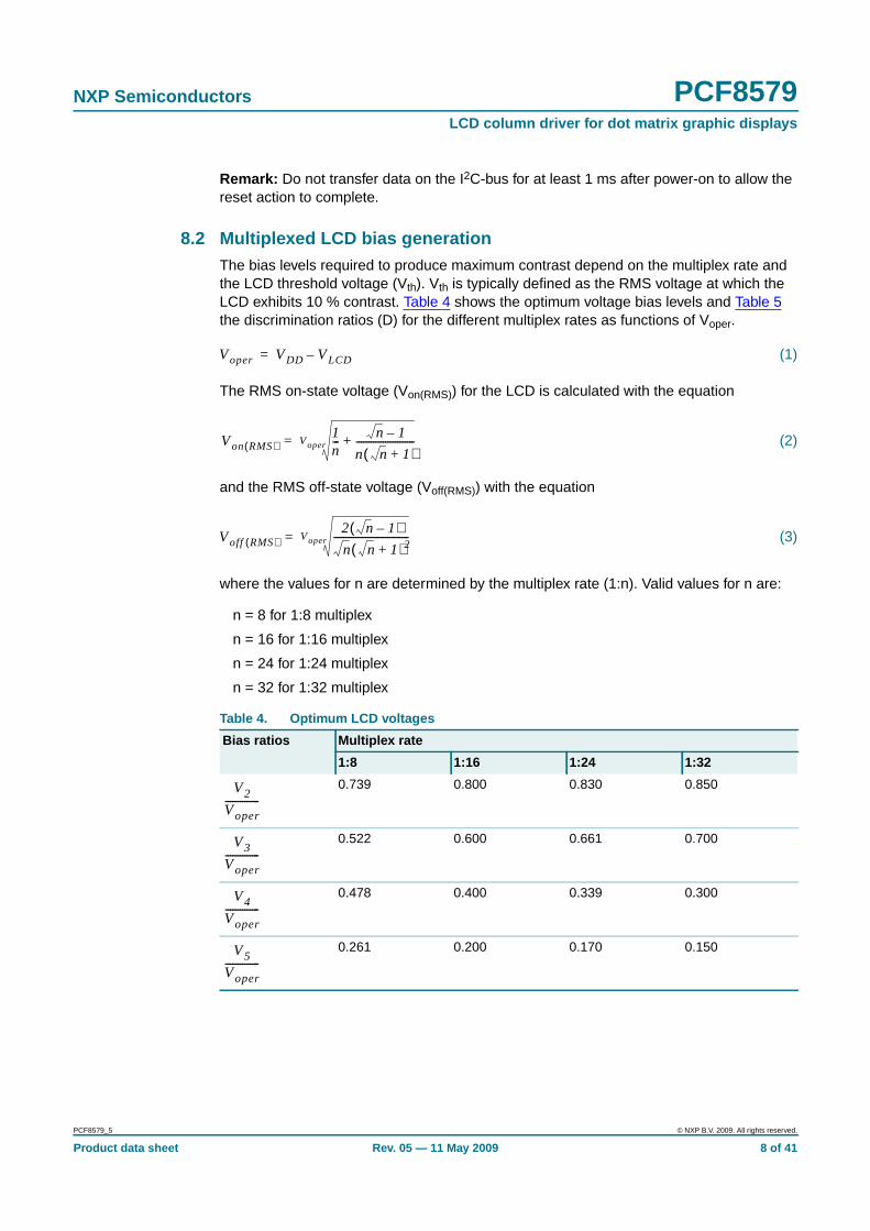
8.2 Multiplexed LCD bias generationThe bias levels required to produce maximum contrast depend on the multiplex rate andthe LCD threshold voltage (Vth). Vth is typically defined as the RMS voltage at which theLCD exhibits 10 % contrast. Table 4 shows the optimum voltage bias levels and Table 5the discrimination ratios (D) for the different multiplex rates as functions of Voper.
(1)
The RMS on-state voltage (Von(RMS)) for the LCD is calculated with the equation
(2)
and the RMS off-state voltage (Voff(RMS)) with the equation
(3)
where the values for n are determined by the multiplex rate (1:n). Valid values for n are:
n = 8 for 1:8 multiplex
n = 16 for 1:16 multiplex
n = 24 for 1:24 multiplex
n = 32 for 1:32 multiplex
Table 4. Optimum LCD voltages
Bias ratios Multiplex rate
1:8 1:16 1:24 1:32
0.739 0.800 0.830 0.850
0.522 0.600 0.661 0.700
0.478 0.400 0.339 0.300
0.261 0.200 0.170 0.150
Voper VDD VLCD–=
Von RMS( )1n---
n 1–
n n 1+( )------------------------+Voper=
Voff RMS( )2 n 1–( )n n 1+( )2
-------------------------------Voper=
V2
Voper--------------
V3
Voper--------------
V4
Voper--------------
V5
Voper--------------
PCF8579_5 © NXP B.V. 2009. All rights reserved.
Product data sheet Rev. 05 — 11 May 2009 8 of 41
NXP Semiconductors PCF8579LCD column driver for dot matrix graphic displays
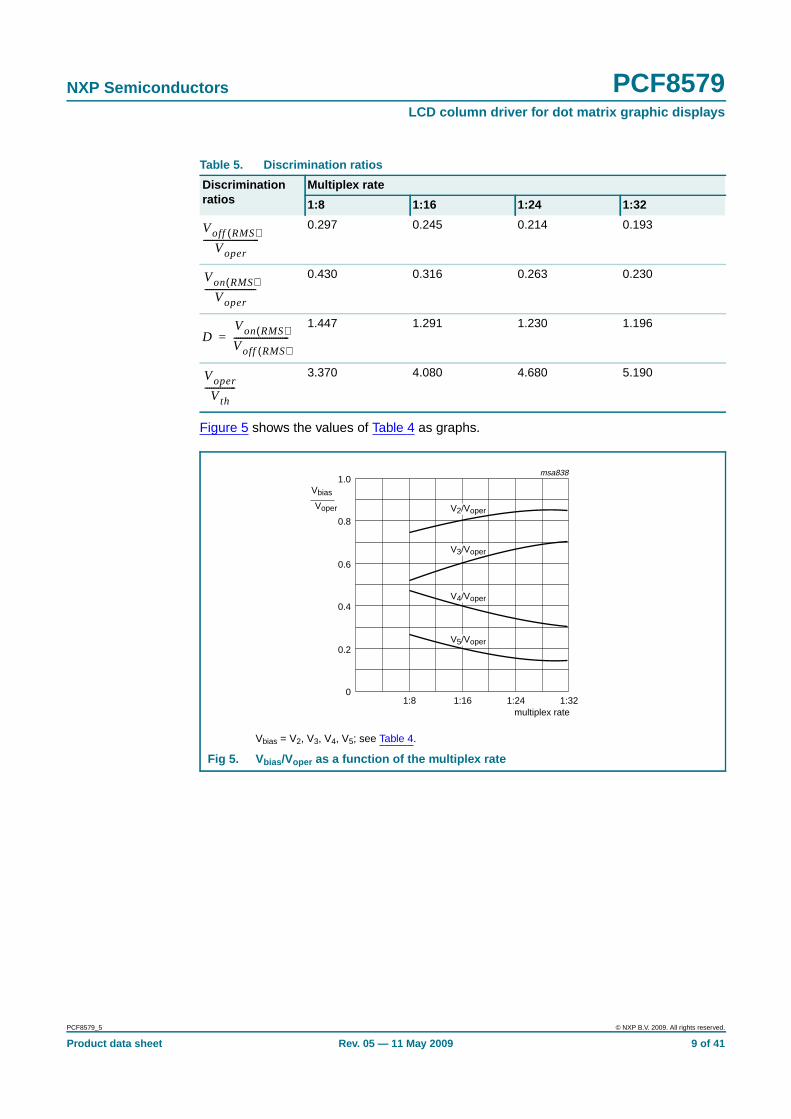
Figure 5 shows the values of Table 4 as graphs.
Table 5. Discrimination ratios
Discriminationratios
Multiplex rate
1:8 1:16 1:24 1:32
0.297 0.245 0.214 0.193
0.430 0.316 0.263 0.230
1.447 1.291 1.230 1.196
3.370 4.080 4.680 5.190
Vbias = V2, V3, V4, V5; see Table 4.
Fig 5. Vbias /Voper as a function of the multiplex rate
Voff RMS( )Voper
-------------------------
Von RMS( )Voper
-----------------------
DVon RMS( )Voff RMS( )-------------------------=
Voper
Vth--------------
1:8 1:16 1:32
1.0
0
0.8
msa838
1:24
0.6
0.4
0.2
multiplex rate
Vbias
Voper V2/Voper
V3/Voper
V4/Voper
V5/Voper
PCF8579_5 © NXP B.V. 2009. All rights reserved.
Product data sheet Rev. 05 — 11 May 2009 9 of 41
NXP Semiconductors PCF8579LCD column driver for dot matrix graphic displays
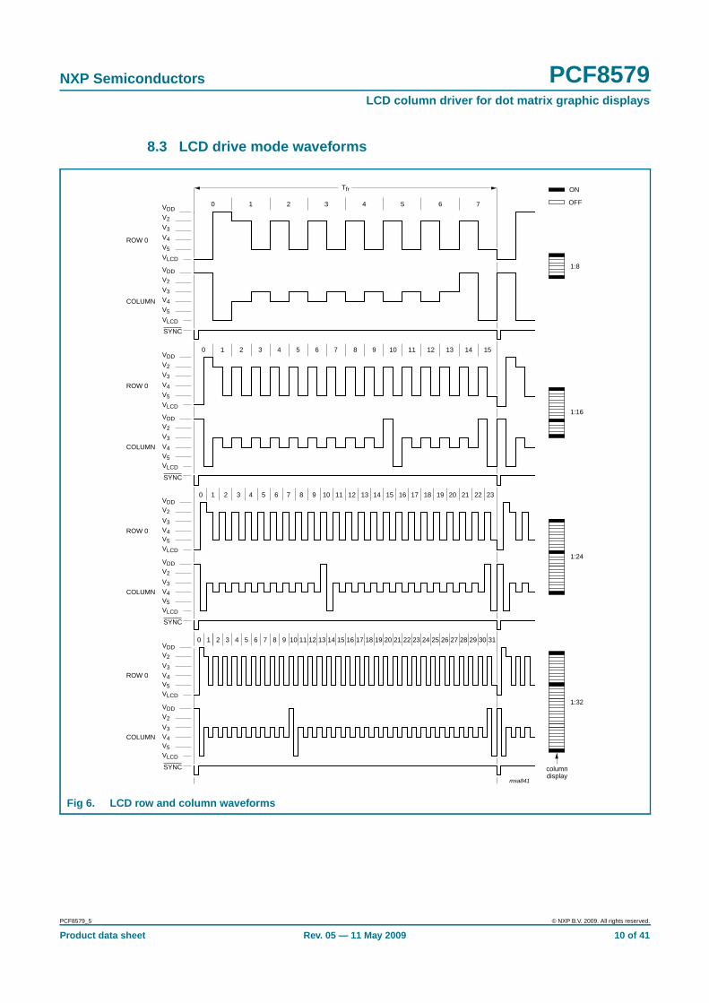
8.3 LCD drive mode waveforms
Fig 6. LCD row and column waveforms
msa841
Tfr
COLUMN
SYNC
ROW 0
0 1 2 3 4 5 6 7 8 9 10 11 12 13 14 15 16 17 18 19 20 21 22 23 24 25 26 27 28 29 30 31
SYNC
COLUMN
ROW 0
23222120191817161514131211109876543210
SYNC
COLUMN
ROW 0
15
SYNC
14131211109876543210
COLUMN
ROW 0
0 1 2 3 4 5 6 7
ON
OFF
1:8
1:16
1:24
1:32
columndisplay
VDD
V2
V3
V4
V5
VLCD
VDD
V2
V3
V4
V5
VLCD
VDD
V2
V3
V4
V5
VLCD
VDDV2
V3
V4V5VLCD
VDDV2
V3V4V5VLCD
VDDV2
V3V4V5VLCD
VDDV2
V3V4V5VLCD
VDDV2
V3V4V5VLCD
PCF8579_5 © NXP B.V. 2009. All rights reserved.
Product data sheet Rev. 05 — 11 May 2009 10 of 41
NXP Semiconductors PCF8579LCD column driver for dot matrix graphic displays
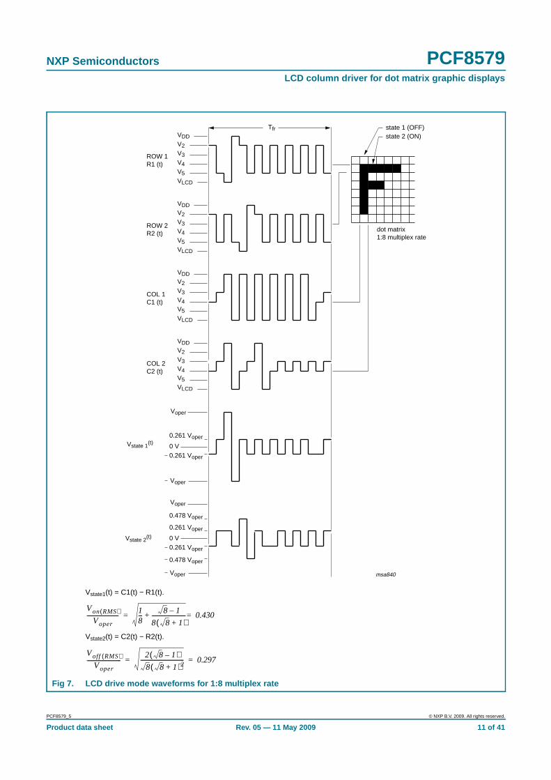
Vstate1(t) = C1(t) − R1(t).
Vstate2(t) = C2(t) − R2(t).
Fig 7. LCD drive mode waveforms for 1:8 multiplex rate
msa840
ROW 1R1 (t)
ROW 2R2 (t)
COL 1C1 (t)
COL 2C2 (t)
dot matrix1:8 multiplex rate
0.261 Voper
0.261 Voper
0 V
0.261 Voper
0.261 Voper
0 V
Voper
0.478 Voper
0.478 Voper
state 1 (OFF)state 2 (ON)VDD
V2V3V4V5VLCD
VDDV2V3V4V5VLCD
VDDV2V3V4V5VLCD
VDDV2V3V4V5VLCD
Tfr
Voper
Voper
Voper
Vstate 1(t)
Vstate 2(t)
Von RMS( )Voper
-----------------------18---
8 1–
8 8 1+( )------------------------+ 0.430==
Voff RMS( )Voper
------------------------2 8 1–( )8 8 1+( )2
------------------------------- 0.297= =
PCF8579_5 © NXP B.V. 2009. All rights reserved.
Product data sheet Rev. 05 — 11 May 2009 11 of 41

NXP Semiconductors PCF8579LCD column driver for dot matrix graphic displays
Vstate1(t) = C1(t) − R1(t).
Vstate2(t) = C2(t) − R2(t).
Fig 8. LCD drive mode waveform for 1:16 multiplex rate
msa836
VDDV2V3V4V5VLCD
VDDV2V3V4V5VLCD
VDDV2V3V4V5VLCD
VDDV2V3V4V5VLCD
Tfr
ROW 1R1 (t)
ROW 2R2 (t)
COL 1C1 (t)
COL 2C2 (t)
dot matrix1:16 multiplex rate
state 1 (OFF)state 2 (ON)
0.2 Voper
0.2 Voper
0 V
Voper
Voper
Vstate 1(t)
Vstate 2(t)
0.2 Voper
0.2 Voper
0 V
Voper
Voper
0.6 Voper
0.6 Voper
Von RMS( )Voper
-----------------------116------
16 1–
16 16 1+( )------------------------------+ 0.316==
Voff RMS( )Voper
------------------------2 16 1–( )16 16 1+( )2
------------------------------------- 0.254= =
PCF8579_5 © NXP B.V. 2009. All rights reserved.
Product data sheet Rev. 05 — 11 May 2009 12 of 41
NXP Semiconductors PCF8579LCD column driver for dot matrix graphic displays
8.4 Timing generatorThe timing generator of the PCF8579 organizes the internal data flow from the RAM to thedisplay drivers. An external synchronization pulse SYNC is received from the PCF8578.This signal maintains the correct timing relationship between cascaded devices.
8.5 Column driversOutputs C0 to C39 are column drivers which must be connected to the LCD. Unusedoutputs should be left open-circuit.
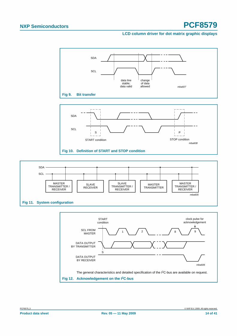
8.6 Characteristics of the I 2C-busThe I2C-bus is for bidirectional, two-line communication between different ICs or modules.The two lines are a Serial Data Line (SDA) and a Serial Clock Line (SCL) which must beconnected to a positive supply via a pull-up resistor. Data transfer may be initiated onlywhen the bus is not busy.
8.6.1 Bit transfer
One data bit is transferred during each clock pulse. The data on the SDA line must remainstable during the HIGH period of the clock pulse as changes in the data line at thismoment will be interpreted as control signals.
8.6.2 START and STOP conditions
Both data and clock lines remain HIGH when the bus is not busy. A HIGH-to-LOWtransition of the data line, while the clock is HIGH, is defined as the START condition (S).A LOW-to-HIGH transition of the data line while the clock is HIGH, is defined as the STOPcondition (P).
8.6.3 System configuration
A device transmitting a message is a transmitter, a device receiving a message is thereceiver. The device that controls the message flow is the master and the devices whichare controlled by the master are the slaves.
8.6.4 Acknowledge
The number of data bytes transferred between the START and STOP conditions fromtransmitter to receiver is unlimited. Each data byte of eight bits is followed by oneacknowledge bit. The acknowledge bit is a HIGH level put on the bus by the transmitter,whereas the master generates an extra acknowledge related clock pulse. A slave receiverwhich is addressed must generate an acknowledge after the reception of each byte. Alsoa master must generate an acknowledge after the reception of each byte that has beenclocked out of the slave transmitter. The device that acknowledges must pull down theSDA line during the acknowledge clock pulse, so that the SDA line is stable LOW duringthe HIGH period of the acknowledge related clock pulse (set-up and hold times must betaken into consideration). A master receiver must signal the end of a data transmission tothe transmitter by not generating an acknowledge on the last byte that has been clockedout of the slave. In this event the transmitter must leave the data line HIGH to enable themaster to generate a STOP condition.
PCF8579_5 © NXP B.V. 2009. All rights reserved.
Product data sheet Rev. 05 — 11 May 2009 13 of 41
NXP Semiconductors PCF8579LCD column driver for dot matrix graphic displays
Fig 9. Bit transfer
Fig 10. Definition of START and STOP condition
mba607
data linestable;
data valid
changeof dataallowed
SDA
SCL
mba608
SDA
SCLP
STOP condition
S
START condition
Fig 11. System configuration
mba605
MASTERTRANSMITTER /
RECEIVER
SLAVERECEIVER
SLAVETRANSMITTER /
RECEIVER
MASTERTRANSMITTER
MASTERTRANSMITTER /
RECEIVER
SDA
SCL
The general characteristics and detailed specification of the I2C-bus are available on request.
Fig 12. Acknowledgement on the I 2C-bus
mba606
STARTcondition
S
SCL FROMMASTER
DATA OUTPUTBY TRANSMITTER
DATA OUTPUTBY RECEIVER
clock pulse foracknowledgement
1 2 8 9
PCF8579_5 © NXP B.V. 2009. All rights reserved.
Product data sheet Rev. 05 — 11 May 2009 14 of 41

NXP Semiconductors PCF8579LCD column driver for dot matrix graphic displays
8.6.5 I2C-bus controller
The I2C-bus controller detects the I2C-bus protocol, slave address, commands and displaydata bytes. It performs the conversion of the data input (serial-to-parallel) and the dataoutput (parallel-to-serial). The PCF8579 acts as an I2C-bus slave transmitter/receiver.Device selection depends on the I2C-bus slave address, the hardware subaddress andthe commands transmitted.
8.6.6 Input filters
To enhance noise immunity in electrically adverse environments, RC low-pass filters areprovided on the SDA and SCL lines.
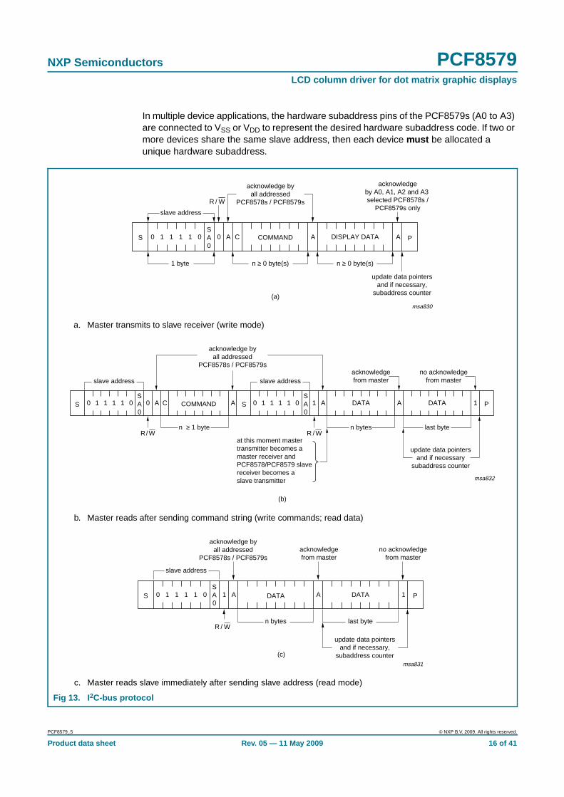
8.6.7 I2C-bus protocol
Two 7-bit slave addresses (0111100 and 0111101) are reserved for both the PCF8578and PCF8579. The least significant bit of the slave address is set by connecting input SA0to either logic 0 (VSS) or logic 1 (VDD). Therefore, two types of PCF8578 or PCF8579 canbe distinguished on the same I2C-bus which allows:
1. One PCF8578 to operate with up to 32 PCF8579s on the same I2C-bus for very largeapplications (see Table 16).
2. The use of two types of LCD multiplex schemes on the same I2C-bus.
In most applications the PCF8578 will have the same slave address as the PCF8579.
The I2C-bus protocol is shown in Figure 13. All communications are initiated with a STARTcondition (S) from the I2C-bus master, which is followed by the desired slave address andread/write bit. All devices with this slave address acknowledge in parallel. All other devicesignore the bus transfer.
In WRITE mode (indicated by setting the read/write bit LOW) one or more commandsfollow the slave address acknowledgement. The commands are also acknowledged by alladdressed devices on the bus. The last command must clear the continuation bit C.After the last command a series of data bytes may follow. The acknowledgement aftereach byte is made only by the (A0, A1, A2 and A3) addressed PCF8579 or PCF8578 withits implicit subaddress 0. After the last data byte has been acknowledged, the I2C-busmaster issues a STOP condition (P).
In READ mode, indicated by setting the read/write bit HIGH, data bytes may be read fromthe RAM following the slave address acknowledgement. After this acknowledgement themaster transmitter becomes a master receiver and the PCF8579 becomes a slavetransmitter. The master receiver must acknowledge the reception of each byte in turn. Themaster receiver must signal an end of data to the slave transmitter, by not generating anacknowledge on the last byte clocked out of the slave. The slave transmitter then leavesthe data line HIGH, enabling the master to generate a STOP condition (P).
Display bytes are written into, or read from the RAM at the address specified by the datapointer and subaddress counter. Both the data pointer and subaddress counter areautomatically incremented, enabling a stream of data to be transferred either to, or fromthe intended devices.
PCF8579_5 © NXP B.V. 2009. All rights reserved.
Product data sheet Rev. 05 — 11 May 2009 15 of 41
NXP Semiconductors PCF8579LCD column driver for dot matrix graphic displays
In multiple device applications, the hardware subaddress pins of the PCF8579s (A0 to A3)are connected to VSS or VDD to represent the desired hardware subaddress code. If two ormore devices share the same slave address, then each device must be allocated aunique hardware subaddress.
a. Master transmits to slave receiver (write mode)
b. Master reads after sending command string (write commands; read data)
c. Master reads slave immediately after sending slave address (read mode)
Fig 13. I2C-bus protocol
msa830
SA0
S 0 1 1 1 1 0 0 A C COMMAND A PADISPLAY DATA
slave address
/R W
acknowledge byall addressed
PCF8578s / PCF8579s
acknowledgeby A0, A1, A2 and A3 selected PCF8578s /
PCF8579s only
n ≥ 0 byte(s)n ≥ 0 byte(s)1 byte
update data pointersand if necessary,
subaddress counter(a)
msa832
SA0
S 0 1 1 1 1 0 0 A C COMMAND A
slave address
/R W
acknowledge byall addressed
PCF8578s / PCF8579s
n ≥ 1 byte
(b)
ADATASA0
S 0 1 1 1 1 0 1 A
slave address
/R W
P1DATA
n bytes last byte
update data pointersand if necessary
subaddress counter
acknowledgefrom master
no acknowledgefrom master
at this moment mastertransmitter becomes amaster receiver andPCF8578/PCF8579 slavereceiver becomes aslave transmitter
msa831
SA0
S 0 1 1 1 1 0 1 A DATA A P1DATA
slave address
/R W
acknowledge byall addressed
PCF8578s / PCF8579s
last byten bytes
update data pointersand if necessary,
subaddress counter(c)
acknowledgefrom master
no acknowledgefrom master
PCF8579_5 © NXP B.V. 2009. All rights reserved.
Product data sheet Rev. 05 — 11 May 2009 16 of 41
NXP Semiconductors PCF8579LCD column driver for dot matrix graphic displays
8.7 Display RAMThe PCF8579 contains a 32 × 40-bit static RAM which stores the display data. The RAMis divided into 4 banks of 40 bytes (4 × 8 × 40 bits). During RAM access, data istransferred to or from the RAM via the I2C-bus.
8.7.1 Data pointer
The addressing mechanism for the display RAM is realized using the data pointer. Thisallows an individual data byte or a series of data bytes to be written into, or read from, thedisplay RAM, controlled by commands sent on the I2C-bus.
8.7.2 Subaddress counter
The storage and retrieval of display data is dependent on the content of the subaddresscounter. Storage and retrieval take place only when the contents of the subaddresscounter matches with the hardware subaddress at pins A0, A1, A2 and A3.
8.8 Command decoderThe command decoder identifies command bytes that arrive on the I2C-bus.
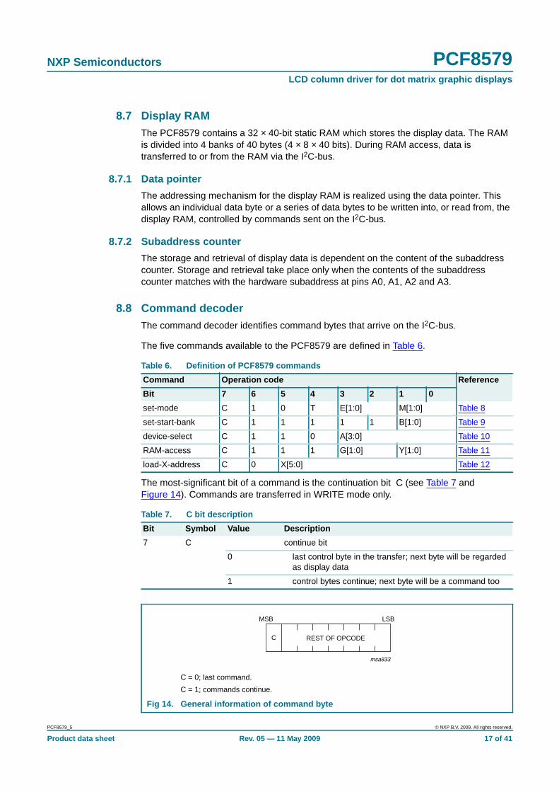
The five commands available to the PCF8579 are defined in Table 6.
The most-significant bit of a command is the continuation bit C (see Table 7 andFigure 14). Commands are transferred in WRITE mode only.
Table 6. Definition of PCF8579 commands
Command Operation code Reference
Bit 7 6 5 4 3 2 1 0
set-mode C 1 0 T E[1:0] M[1:0] Table 8
set-start-bank C 1 1 1 1 1 B[1:0] Table 9
device-select C 1 1 0 A[3:0] Table 10
RAM-access C 1 1 1 G[1:0] Y[1:0] Table 11
load-X-address C 0 X[5:0] Table 12
Table 7. C bit description
Bit Symbol Value Description
7 C continue bit
0 last control byte in the transfer; next byte will be regardedas display data
1 control bytes continue; next byte will be a command too
C = 0; last command.
C = 1; commands continue.
Fig 14. General information of command byte
msa833
REST OF OPCODEC
MSB LSB
PCF8579_5 © NXP B.V. 2009. All rights reserved.
Product data sheet Rev. 05 — 11 May 2009 17 of 41
NXP Semiconductors PCF8579LCD column driver for dot matrix graphic displays
[1] Useful for scrolling, pseudo-motion and background preparation of new display content.
[1] Values shown in decimal.
Table 8. Set-mode - command bit description
Bit Symbol Value Description
7 C 0, 1 see Table 7
6, 5 - 10 fixed value
4 T display mode
0 PCF8578 row only
1 PCF8578 mixed mode
3, 2 E[1:0] display status
00 blank
01 normal
10 all segments on
11 inverse video
1, 0 M[1:0] LCD drive mode
01 1:8 MUX (8 rows)
10 1:16 MUX (16 rows)
11 1:24 MUX (24 rows)
00 1:32 MUX (32 rows)
Table 9. Set-start-bank - command bit description
Bit Symbol Value Description
7 C 0, 1 see Table 7
6 to 2 - 11111 fixed value
1, 0 B[1:0] start bank pointer (see Figure 18)[1]
00 bank 0
01 bank 1
10 bank 2
11 bank 3
Table 10. Device-select - command bit description
Bit Symbol Value Description
7 C 0, 1 see Table 7
6 to 4 - 110 fixed value
3 to 0 A[3:0] 0 to 15[1] hardware subaddress;
4 bit binary value; transferred to the subaddresscounter to define one of sixteen hardwaresubaddresses
PCF8579_5 © NXP B.V. 2009. All rights reserved.
Product data sheet Rev. 05 — 11 May 2009 18 of 41
NXP Semiconductors PCF8579LCD column driver for dot matrix graphic displays
[1] See operation code for set-start-bank in Table 9.
[2] Values shown in decimal.
[1] Values shown in decimal.
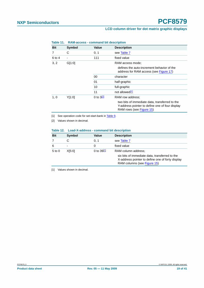
Table 11. RAM-access - command bit description
Bit Symbol Value Description
7 C 0, 1 see Table 7
6 to 4 - 111 fixed value
3, 2 G[1:0] RAM access mode;
defines the auto-increment behavior of theaddress for RAM access (see Figure 17)
00 character
01 half-graphic
10 full-graphic
11 not allowed[1]
1, 0 Y[1:0] 0 to 3[2] RAM row address;
two bits of immediate data, transferred to theY-address pointer to define one of four displayRAM rows (see Figure 15)
Table 12. Load-X-address - command bit description
Bit Symbol Value Description
7 C 0, 1 see Table 7
6 - 0 fixed value
5 to 0 X[5:0] 0 to 39[1] RAM column address;
six bits of immediate data, transferred to theX-address pointer to define one of forty displayRAM columns (see Figure 15)
PCF8579_5 © NXP B.V. 2009. All rights reserved.
Product data sheet Rev. 05 — 11 May 2009 19 of 41
NXP Semiconductors PCF8579LCD column driver for dot matrix graphic displays
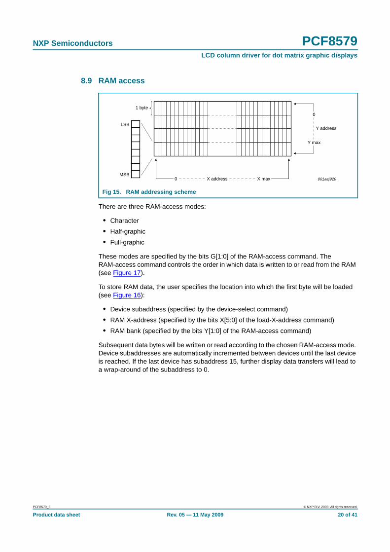
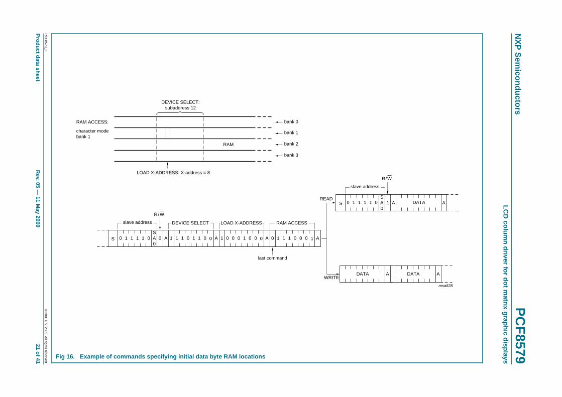
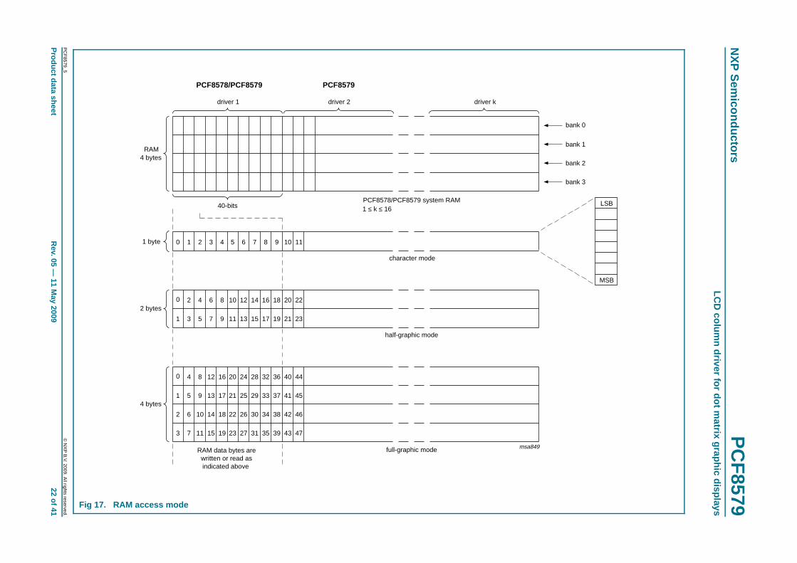
8.9 RAM access
There are three RAM-access modes:
• Character
• Half-graphic
• Full-graphic
These modes are specified by the bits G[1:0] of the RAM-access command. TheRAM-access command controls the order in which data is written to or read from the RAM(see Figure 17).
To store RAM data, the user specifies the location into which the first byte will be loaded(see Figure 16):
• Device subaddress (specified by the device-select command)
• RAM X-address (specified by the bits X[5:0] of the load-X-address command)
• RAM bank (specified by the bits Y[1:0] of the RAM-access command)
Subsequent data bytes will be written or read according to the chosen RAM-access mode.Device subaddresses are automatically incremented between devices until the last deviceis reached. If the last device has subaddress 15, further display data transfers will lead toa wrap-around of the subaddress to 0.
Fig 15. RAM addressing scheme
001aaj920
LSB
1 byte
0 X address X max
0
Y max
Y address
MSB
PCF8579_5 © NXP B.V. 2009. All rights reserved.
Product data sheet Rev. 05 — 11 May 2009 20 of 41
xxxxxxxxxxxxxxxxxxxxx xxxxxxxxxxxxxxxxxxxxxxxxxx xxxxxxx x x x xxxxxxxxxxxxxxxxxxxxxxxxxxxxxx xxxxxxxxxxxxxxxxxxx xx xxxxxxx xxxxxxxxxxxxxxxxxxxxxxxxxxx xxxxxxxxxxxxxxxxxxx xxxxxx xxxxxxxxxxxxxxxxxxxxxxxxxxxxxxxxxxx xxxxxxxxxxxx x xxxxxxxxxxxxxxxxxxxxxx xxxxxxxxxxxxxxxxxxxxxxxxxxxxxx xxxxx xxxxxxxxxxxxxxxxxxxxxxxxxxxxxxxxxxxxxxxxxxxxxxxxxx xxxxxxxxxxxxxxxxxxxxxxxxxxxxxxxxx xxxxxxxxxxxxxxxxxxxx xxx
PC
F8579_5
Product data shee
NX
P S
emiconductors
PC
F8579
LCD
column driver for dot m
atrix graphic displays
msa835
SA0
0 1 A
ress
/R W
DATA A
A DATA A
© N
XP
B.V. 2009. A
ll rights reserved.
tR
ev. 05 — 11 M
ay 200921 of 41 Fig 16. Example of commands specifying initial data byte RAM locations
SA0
S 0 1 1 1 1 0 0 A
slave address
/R W
01 1 0 1 1 0 A
DEVICE SELECT
1 00 0 0 1 0 0 A
LOAD X-ADDRESS
1 11 1 1 0 0 0 A
RAM ACCESS
0
last command
S 0 1 1 1 1
slave add
READ
WRITEDATA
DEVICE SELECT:subaddress 12
RAM ACCESS:
character modebank 1
LOAD X-ADDRESS: X-address = 8
RAM
bank 0
bank 1
bank 2
bank 3
xxxxxxxxxxxxxxxxxxxxx xxxxxxxxxxxxxxxxxxxxxxxxxx xxxxxxx x x x xxxxxxxxxxxxxxxxxxxxxxxxxxxxxx xxxxxxxxxxxxxxxxxxx xx xxxxxxx xxxxxxxxxxxxxxxxxxxxxxxxxxx xxxxxxxxxxxxxxxxxxx xxxxxx xxxxxxxxxxxxxxxxxxxxxxxxxxxxxxxxxxx xxxxxxxxxxxx x xxxxxxxxxxxxxxxxxxxxxx xxxxxxxxxxxxxxxxxxxxxxxxxxxxxx xxxxx xxxxxxxxxxxxxxxxxxxxxxxxxxxxxxxxxxxxxxxxxxxxxxxxxx xxxxxxxxxxxxxxxxxxxxxxxxxxxxxxxxx xxxxxxxxxxxxxxxxxxxx xxx
PC
F8579_5
Product data shee
NX
P S
emiconductors
PC
F8579
LCD
column driver for dot m
atrix graphic displays
a849
LSB
MSB
bank 0
bank 1
bank 2
bank 3
driver 1 driver 2 driver k
PCF8578/PCF8579 PCF8579
© N
XP
B.V. 2009. A
ll rights reserved.
tR
ev. 05 — 11 M
ay 200922 of 41 Fig 17. RAM access mode
ms
0 1 2 3 4 5 6 7 8 9 10 11
0 2 4 6 8 10 12 14 16 18 20 22
1 3 5 7 9 11 13 15 17 19 21 23
0 4 8 12 16 20 24 28 32 36 40 44
1 5 9 13 17 21 25 29 33 37 41 45
2 6 10 14 18 22 26 30 34 38 42 46
3 7 11 15 19 23 27 31 35 39 43 47
RAM data bytes arewritten or read asindicated above
full-graphic mode
PCF8578/PCF8579 system RAM1 ≤ k ≤ 16
half-graphic mode
character mode
1 byte
4 bytesRAM
2 bytes
4 bytes
40-bits
NXP Semiconductors PCF8579LCD column driver for dot matrix graphic displays
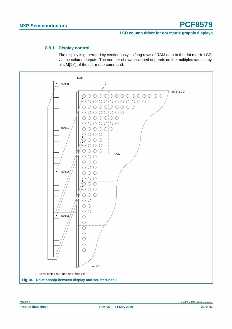
8.9.1 Display control
The display is generated by continuously shifting rows of RAM data to the dot matrix LCDvia the column outputs. The number of rows scanned depends on the multiplex rate set bybits M[1:0] of the set-mode command.
1:32 multiplex rate and start bank = 2.
Fig 18. Relationship between display and set-start-bank
msa851
bank 0
top of LCD
bank 1
bank 2
bank 3
LCD
RAM
PCF8579_5 © NXP B.V. 2009. All rights reserved.
Product data sheet Rev. 05 — 11 May 2009 23 of 41
NXP Semiconductors PCF8579LCD column driver for dot matrix graphic displays
The display status (all dots on or off and normal or inverse video) is set by the bits E[1:0]of the set-mode command. For bank switching, the RAM bank corresponding to the top ofthe display is set by the bits B[1:0] of the set-start-bank command. This is shown inFigure 18. This feature is useful when scrolling in alphanumeric applications.
9. Limiting values
[1] According to the NXP store and transport conditions (document SNW-SQ-623) the devices have to bestored at a temperature of +5 °C to +45 °C and a humidity of 25 % to 75 %.
Table 13. Limiting valuesIn accordance with the Absolute Maximum Rating System (IEC 60134).
Symbol Parameter Conditions Min Max Unit
VDD supply voltage −0.5 +8.0 V
VLCD LCD supply voltage VDD − 11 +8.0 V
VI input voltage VDD related;
on pins SDA, SCL,CLK, TEST, SA0and OSC
−0.5 +8.0 V
VLCD related;
V3 and V4
VDD − 11 +8.0 V
VO output voltage VDD related;
SYNC and CLK
−0.5 +8.0 V
VLCD related;
R0 to R7, R8/C8 toR31/C31 and C32to C39
VDD − 11 +8.0 V
II input current −10 +10 mA
IO output current −10 +10 mA
IDD supply current −50 +50 mA
IDD(LCD) LCD supply current −50 +50 mA
ISS ground supply current −50 +50 mA
Ptot total power dissipation per package - 400 mW
Po output power - 100 mW
Tstg storage temperature [1] −65 +150 °C
PCF8579_5 © NXP B.V. 2009. All rights reserved.
Product data sheet Rev. 05 — 11 May 2009 24 of 41
NXP Semiconductors PCF8579LCD column driver for dot matrix graphic displays
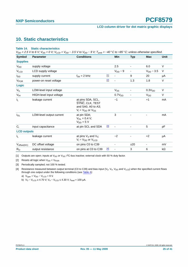
10. Static characteristics
[1] Outputs are open; inputs at VDD or VSS; I2C-bus inactive; external clock with 50 % duty factor.
[2] Resets all logic when VDD < VPOR.
[3] Periodically sampled; not 100 % tested.
[4] Resistance measured between output terminal (C0 to C39) and bias input (V3, V4, VDD and VLCD) when the specified current flowsthrough one output under the following conditions (see Table 4):
a) Voper = VDD − VLCD = 9 V.
b) V3 − VLCD ≥ 4.70 V; V4 − VLCD ≤ 4.30 V; Iload = 100 µA.
Table 14. Static characteristicsVDD = 2.5 V to 6 V; VSS = 0 V; VLCD = VDD − 3.5 V to VDD − 9 V; Tamb = −40 °C to +85 °C; unless otherwise specified.
Symbol Parameter Conditions Min Typ Max Unit
Supplies
VDD supply voltage 2.5 - 6.0 V
VLCD LCD supply voltage VDD − 9 - VDD − 3.5 V
IDD supply current fclk = 2 kHz [1] - 9 20 µA
VPOR power-on reset voltage [2] - 1.3 1.8 V
Logic
VIL LOW-level input voltage VSS - 0.3VDD V
VIH HIGH-level input voltage 0.7VDD - VDD V
IL leakage current at pins SDA, SCL,SYNC, CLK, TESTand SA0, A0 to A3;Vi = VDD or VSS
−1 - +1 mA
IOL LOW-level output current at pin SDA;VOL = 0.4 V;VDD = 5 V
3 - - mA
Ci input capacitance at pin SCL and SDA [3] - - 5 pF
LCD outputs
IL leakage current at pins V3 and V4;Vi = VDD or VLCD
−2 - +2 µA
Voffset(DC) DC offset voltage on pins C0 to C39 - ±20 - mV
RO output resistance on pins at C0 to C39 [4] - 3 6 kΩ
PCF8579_5 © NXP B.V. 2009. All rights reserved.
Product data sheet Rev. 05 — 11 May 2009 25 of 41
NXP Semiconductors PCF8579LCD column driver for dot matrix graphic displays
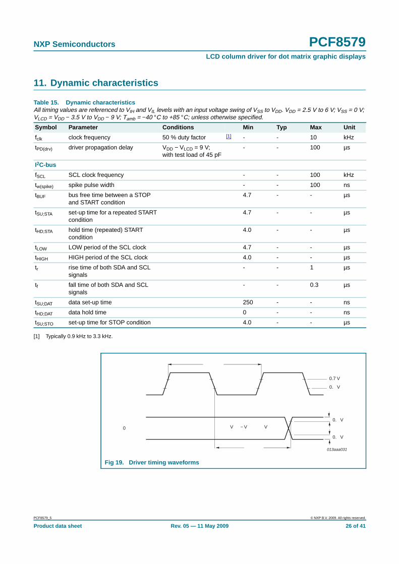
11. Dynamic characteristics
[1] Typically 0.9 kHz to 3.3 kHz.
Table 15. Dynamic characteristicsAll timing values are referenced to VIH and VIL levels with an input voltage swing of VSS to VDD. VDD = 2.5 V to 6 V; VSS = 0 V;VLCD = VDD − 3.5 V to VDD − 9 V; Tamb = −40 °C to +85 °C; unless otherwise specified.
Symbol Parameter Conditions Min Typ Max Unit
fclk clock frequency 50 % duty factor [1] - - 10 kHz
tPD(drv) driver propagation delay VDD − VLCD = 9 V;with test load of 45 pF
- - 100 µs
I2C-bus
fSCL SCL clock frequency - - 100 kHz
tw(spike) spike pulse width - - 100 ns
tBUF bus free time between a STOPand START condition
4.7 - - µs
tSU;STA set-up time for a repeated STARTcondition
4.7 - - µs
tHD;STA hold time (repeated) STARTcondition
4.0 - - µs
tLOW LOW period of the SCL clock 4.7 - - µs
tHIGH HIGH period of the SCL clock 4.0 - - µs
tr rise time of both SDA and SCLsignals
- - 1 µs
tf fall time of both SDA and SCLsignals
- - 0.3 µs
tSU;DAT data set-up time 250 - - ns
tHD;DAT data hold time 0 - - ns
tSU;STO set-up time for STOP condition 4.0 - - µs
Fig 19. Driver timing waveforms
013aaa031
0.7 VDD
0.3 V DD
1/ f clk
CLK
0.5 V
0.5 V
tPD(drv)
C0 to C39 (VDD − VLCD = 9 V)
PCF8579_5 © NXP B.V. 2009. All rights reserved.
Product data sheet Rev. 05 — 11 May 2009 26 of 41
NXP Semiconductors PCF8579LCD column driver for dot matrix graphic displays
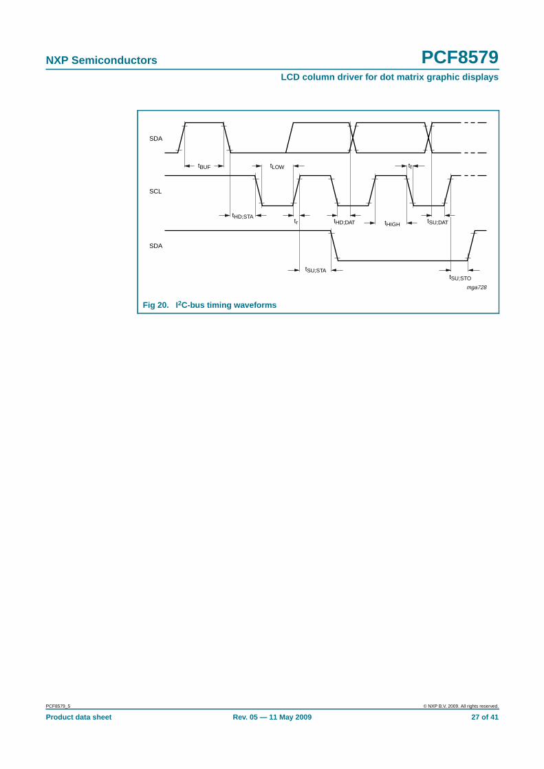
Fig 20. I2C-bus timing waveforms
SDA
mga728
SDA
SCL
tSU;STAtSU;STO
tHD;STA
tBUF tLOW
tHD;DAT tHIGHtr
tf
tSU;DAT
PCF8579_5 © NXP B.V. 2009. All rights reserved.
Product data sheet Rev. 05 — 11 May 2009 27 of 41
NXP Semiconductors PCF8579LCD column driver for dot matrix graphic displays
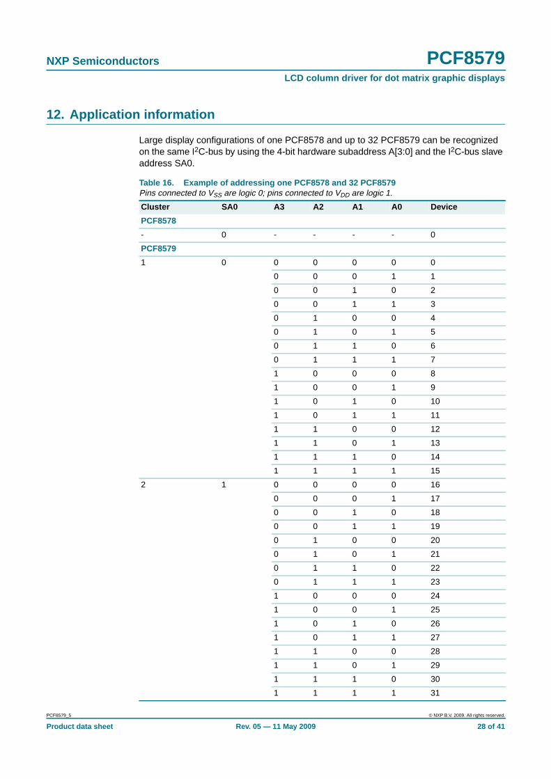
12. Application information
Large display configurations of one PCF8578 and up to 32 PCF8579 can be recognizedon the same I2C-bus by using the 4-bit hardware subaddress A[3:0] and the I2C-bus slaveaddress SA0.
Table 16. Example of addressing one PCF8578 and 32 PCF8579Pins connected to VSS are logic 0; pins connected to VDD are logic 1.
Cluster SA0 A3 A2 A1 A0 Device
PCF8578
- 0 - - - - 0
PCF8579
1 0 0 0 0 0 0
0 0 0 1 1
0 0 1 0 2
0 0 1 1 3
0 1 0 0 4
0 1 0 1 5
0 1 1 0 6
0 1 1 1 7
1 0 0 0 8
1 0 0 1 9
1 0 1 0 10
1 0 1 1 11
1 1 0 0 12
1 1 0 1 13
1 1 1 0 14
1 1 1 1 15
2 1 0 0 0 0 16
0 0 0 1 17
0 0 1 0 18
0 0 1 1 19
0 1 0 0 20
0 1 0 1 21
0 1 1 0 22
0 1 1 1 23
1 0 0 0 24
1 0 0 1 25
1 0 1 0 26
1 0 1 1 27
1 1 0 0 28
1 1 0 1 29
1 1 1 0 30
1 1 1 1 31
PCF8579_5 © NXP B.V. 2009. All rights reserved.
Product data sheet Rev. 05 — 11 May 2009 28 of 41
xxxxxxxxxxxxxxxxxxxxx xxxxxxxxxxxxxxxxxxxxxxxxxx xxxxxxx x x x xxxxxxxxxxxxxxxxxxxxxxxxxxxxxx xxxxxxxxxxxxxxxxxxx xx xxxxxxx xxxxxxxxxxxxxxxxxxxxxxxxxxx xxxxxxxxxxxxxxxxxxx xxxxxx xxxxxxxxxxxxxxxxxxxxxxxxxxxxxxxxxxx xxxxxxxxxxxx x xxxxxxxxxxxxxxxxxxxxxx xxxxxxxxxxxxxxxxxxxxxxxxxxxxxx xxxxx xxxxxxxxxxxxxxxxxxxxxxxxxxxxxxxxxxxxxxxxxxxxxxxxxx xxxxxxxxxxxxxxxxxxxxxxxxxxxxxxxxx xxxxxxxxxxxxxxxxxxxx xxx
PC
F8579_5
Product data shee
NX
P S
emiconductors
PC
F8579
LCD
column driver for dot m
atrix graphic displays
VLCD
VDD
VSS
VSS
VSS
V3
V4
SCL SDA SA0CLKSYNC
A0
A1
A2
A3
PCF8579#k
40columns subaddress k−1
≤ 16)
msa845
© N
XP
B.V. 2009. A
ll rights reserved.
tR
ev. 05 — 11 M
ay 200929 of 41
Fig 21. Typical LCD driver system with 1:32 multiplex rate
Rext(OSC)OSC
SCL SDA SA0CLKSYNC
A0
A1
A2
A3
PCF8579#1
40columns subaddress 0
SCLSDA
SA0
CLK SYNC
PCF8578(ROW MODE)
VDD
VDD
VLCD
VLCD VLCD VLCD
VDD
VDD VDD VDD VDD VDD
VSS
VSS
VSS VSS VSS VSS VSS
VSS
VSS
VSS
V2
V3
V3
V4
V4
V3
V4
V5
unused columns
8
SCLSDA
32
rows
R
R
R
R
C
C
C
C
C
SCL SDA SA0CLKSYNC
A0
A1
A2
A3
PCF8579#2
40columns subaddress 1
1:32 multiplex rate32 × 40 × k dots (k(20480 dots max.)
LCD DISPLAY
(4 2 3)R
xxxxxxxxxxxxxxxxxxxxx xxxxxxxxxxxxxxxxxxxxxxxxxx xxxxxxx x x x xxxxxxxxxxxxxxxxxxxxxxxxxxxxxx xxxxxxxxxxxxxxxxxxx xx xxxxxxx xxxxxxxxxxxxxxxxxxxxxxxxxxx xxxxxxxxxxxxxxxxxxx xxxxxx xxxxxxxxxxxxxxxxxxxxxxxxxxxxxxxxxxx xxxxxxxxxxxx x xxxxxxxxxxxxxxxxxxxxxx xxxxxxxxxxxxxxxxxxxxxxxxxxxxxx xxxxx xxxxxxxxxxxxxxxxxxxxxxxxxxxxxxxxxxxxxxxxxxxxxxxxxx xxxxxxxxxxxxxxxxxxxxxxxxxxxxxxxxx xxxxxxxxxxxxxxxxxxxx xxx
PC
F8579_5
Product data shee
NX
P S
emiconductors
PC
F8579
LCD
column driver for dot m
atrix graphic displays
SCLSDA CLK SYNC
PCF8579#1
40columns
SCL SDA SA0CLKSYNC
A0
A1
A2
A3
PCF8579#k
40columns subaddress k 1
msa847
V3
V4
VDD VDD
VSS
VSS
VLCD
VSS
© N
XP
B.V. 2009. A
ll rights reserved.
tR
ev. 05 — 11 M
ay 200930 of 41
Fig 22. Split screen application with 1:16 multiplex rate for improved contrast
OSC
SCL SDA SA0CLKSYNC
A0
A1
A2
A3
PCF8579#1
40columns subaddress 0
SCLSDA
SA0
CLK SYNC
PCF8578(ROW MODE) unused columns
16
8
rows
SCLSDA
1:16 multiplex rate16 × 40 × k dots (k ≤ 16)(10240 dots max.)
16
rows
R
R
R
R
R
C
C
C
C
C
SA0
A0
A1
A2
A3
subaddress 0
SCLSDASA0 CLK SYNC
A0
A1
A2
A3
PCF8579
40columns
subaddress k 1
#k
SCL SDA SA0CLKSYNC
A0
A1
A2
A3
PCF8579#2
40columns subaddress 1
1:16 multiplex rate16 × 40 × k dots (k ≤ 16)(10240 dots max.)
LCD DISPLAY
SCLSDASA0 CLK SYNC
A0
A1
A2
A3
PCF8579#2
40columns
subaddress 1
Rext(OSC)
V3
V4
VDD
VDD VDD
VSS
VSS
VLCD
V3
V4
VDD
VDD VDD
VSS
VSS
VLCD
VDD
V3
V4
VDDVDD
VSS
VSS
VLCD
V3
V4
VDDVDD
VSS
VSS
VSS
VLCD
V3
V4
VDDVDD
VSS
VSS
VSS
VLCD
V3
V2
V4
V5
VDD
VDD
VDD
VSS
VSS
VSS/VDD
VSS
VLCD
VLCD
xxxxxxxxxxxxxxxxxxxxx xxxxxxxxxxxxxxxxxxxxxxxxxx xxxxxxx x x x xxxxxxxxxxxxxxxxxxxxxxxxxxxxxx xxxxxxxxxxxxxxxxxxx xx xxxxxxx xxxxxxxxxxxxxxxxxxxxxxxxxxx xxxxxxxxxxxxxxxxxxx xxxxxx xxxxxxxxxxxxxxxxxxxxxxxxxxxxxxxxxxx xxxxxxxxxxxx x xxxxxxxxxxxxxxxxxxxxxx xxxxxxxxxxxxxxxxxxxxxxxxxxxxxx xxxxx xxxxxxxxxxxxxxxxxxxxxxxxxxxxxxxxxxxxxxxxxxxxxxxxxx xxxxxxxxxxxxxxxxxxxxxxxxxxxxxxxxx xxxxxxxxxxxxxxxxxxxx xxx
PC
F8579_5
Product data shee
NX
P S
emiconductors
PC
F8579
LCD
column driver for dot m
atrix graphic displays
SCLSDA CLK SYNC
PCF8579#1
40columns
V3
V4
VDD VDD
VSS
VSS
VLCD
VSS
SCL SDA SA0CLKSYNC
A0
A1
A2
A3
PCF8579#k
40columns subaddress k 1
32
msa846
© N
XP
B.V. 2009. A
ll rights reserved.
tR
ev. 05 — 11 M
ay 200931 of 41
Fig 23. Split screen application with 1:32 multiplex rate
Rext(OSC)
OSC
SCL SDA SA0CLKSYNC
A0
A1
A2
A3
PCF8579#1
40columns subaddress 0
SCLSDA
SA0
CLK SYNC
PCF8578(ROW MODE) unused columns
8
SCLSDA
1:32 multiplex rate32 × 40 × k dots (k ≤ 16)(20480 dots max.)
32
rows
R
R
R
R
C
C
C
C
C
SA0
A0
A1
A2
A3
subaddress 0
SCLSDASA0 CLK SYNC
V3
V4
A0
A1
A2
A3
PCF8579
40columns
VDD
VDD VDD
VSS
VSS
VLCD
V3
V4
VDD
VDD VDD
VSS
VSS
VLCD
VDD
V3
V4
VDDVDD
VSS
VSS
VLCD
V3
V4
VDDVDD
VSS
VSS
VSS
VLCD
V3
V4
VDDVDD
VSS
VSS
VSS
VLCD
V3
V2
V4
V5
VDD
VDD
VDD
VSS
VSS
VSS/VDD
VSS
VLCD
VLCD
subaddress k 1
#k
SCL SDA SA0CLKSYNC
A0
A1
A2
A3
PCF8579#2
40columns subaddress 1
1:32 multiplex rate32 × 40 × k dots (k ≤ 16)(20480 dots max.)
LCD DISPLAY
SCLSDASA0 CLK SYNC
A0
A1
A2
A3
PCF8579#2
40columns
subaddress 1
(4 2 3)R
xxxxxxxxxxxxxxxxxxxxx xxxxxxxxxxxxxxxxxxxxxxxxxx xxxxxxx x x x xxxxxxxxxxxxxxxxxxxxxxxxxxxxxx xxxxxxxxxxxxxxxxxxx xx xxxxxxx xxxxxxxxxxxxxxxxxxxxxxxxxxx xxxxxxxxxxxxxxxxxxx xxxxxx xxxxxxxxxxxxxxxxxxxxxxxxxxxxxxxxxxx xxxxxxxxxxxx x xxxxxxxxxxxxxxxxxxxxxx xxxxxxxxxxxxxxxxxxxxxxxxxxxxxx xxxxx xxxxxxxxxxxxxxxxxxxxxxxxxxxxxxxxxxxxxxxxxxxxxxxxxx xxxxxxxxxxxxxxxxxxxxxxxxxxxxxxxxx xxxxxxxxxxxxxxxxxxxx xxx
PC
F8579_5
Product data shee
NX
P S
emiconductors
PC
F8579
LCD
column driver for dot m
atrix graphic displaysSDA VLCD
SCL
VSS
VDD
msa852
R0
n.c.
C27 C28 C39
PCF8579
to otherPCF8579s
© N
XP
B.V. 2009. A
ll rights reserved.
tR
ev. 05 — 11 M
ay 200932 of 41
Fig 24. Example of single plane wiring, single screen with 1:32 multiplex rate (PCF8578 in row driver mode)
PCF8578
LCD DISPLAY
Rext(OSC)
n.c.n.c.
R31/C31
RRRR(4 2 3)R
n.c.
C0 C27 C28 C39
PCF8579
C0
NXP Semiconductors PCF8579LCD column driver for dot matrix graphic displays
13. Package outline
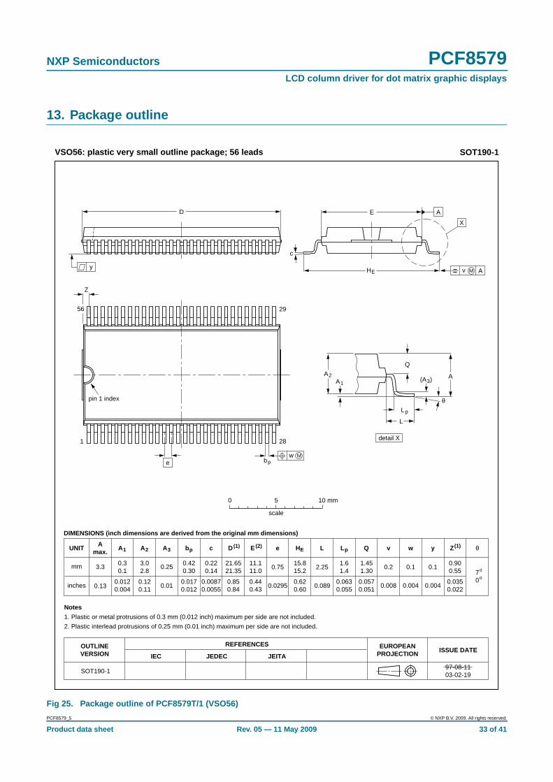
Fig 25. Package outline of PCF8579T/1 (VSO56)
UNIT A1 A2 A3 bp c D (1) E(2) (1)e HE L L p Q Zywv θ
REFERENCESOUTLINEVERSION
EUROPEANPROJECTION ISSUE DATE
IEC JEDEC JEITA
mm
inches
0.30.1
3.02.8
0.250.420.30
0.220.14
21.6521.35
11.111.0
0.7515.815.2
1.451.30
0.900.55 7
0
o
o
0.1 0.1
DIMENSIONS (inch dimensions are derived from the original mm dimensions)
1.61.4
SOT190-197-08-1103-02-19
w M
θ
AA1
A2
bp
D
HE
Lp
Q
detail X
E
Z
e
c
L
v M A
X
(A )3
A
y
56 29
281
pin 1 index
0.0120.004
0.120.11
0.0170.012
0.00870.0055
0.850.84
0.440.43
0.0295
2.25
0.0890.620.60
0.0570.051
0.0350.022
0.004
0.2
0.008 0.0040.0630.055
0.01
0 5 10 mm
scale
VSO56: plastic very small outline package; 56 leads SOT190-1
Amax.
3.3
0.13
Notes
1. Plastic or metal protrusions of 0.3 mm (0.012 inch) maximum per side are not included.
2. Plastic interlead protrusions of 0.25 mm (0.01 inch) maximum per side are not included.
PCF8579_5 © NXP B.V. 2009. All rights reserved.
Product data sheet Rev. 05 — 11 May 2009 33 of 41
NXP Semiconductors PCF8579LCD column driver for dot matrix graphic displays
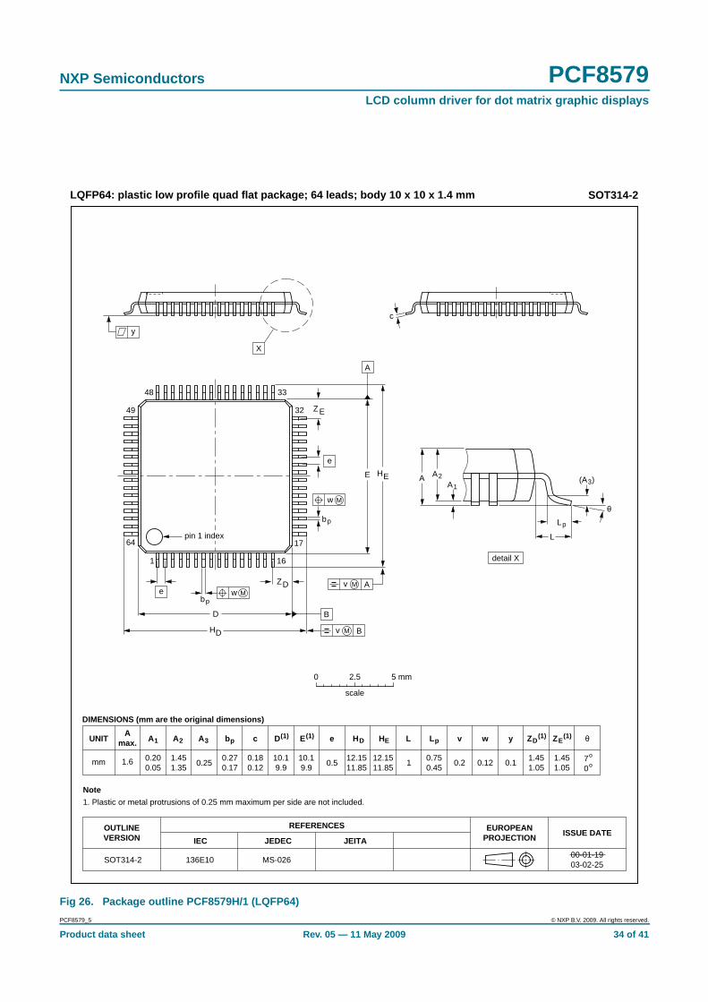
Fig 26. Package outline PCF8579H/1 (LQFP64)
UNITA
max. A1 A2 A3 bp c E(1) e HE L L p Zywv θ
REFERENCESOUTLINEVERSION
EUROPEANPROJECTION ISSUE DATE
IEC JEDEC JEITA
mm 1.6 0.200.05
1.451.35
0.250.270.17
0.180.12
10.19.9
0.512.1511.85
1.451.05
70
o
o0.12 0.11 0.2
DIMENSIONS (mm are the original dimensions)
Note
1. Plastic or metal protrusions of 0.25 mm maximum per side are not included.
0.750.45
SOT314-2 MS-026136E1000-01-1903-02-25
D(1) (1)(1)
10.19.9
HD
12.1511.85
EZ
1.451.05
D
bpe
θ
EA1
A
Lp
detail X
L
(A )3
B
16
c
DH
bp
EH A2
v M B
D
ZD
A
ZE
e
v M A
X
1
64
49
48 33
32
17
y
pin 1 index
w M
w M
0 2.5 5 mm
scale
LQFP64: plastic low profile quad flat package; 64 leads; body 10 x 10 x 1.4 mm SOT314-2
PCF8579_5 © NXP B.V. 2009. All rights reserved.
Product data sheet Rev. 05 — 11 May 2009 34 of 41
NXP Semiconductors PCF8579LCD column driver for dot matrix graphic displays
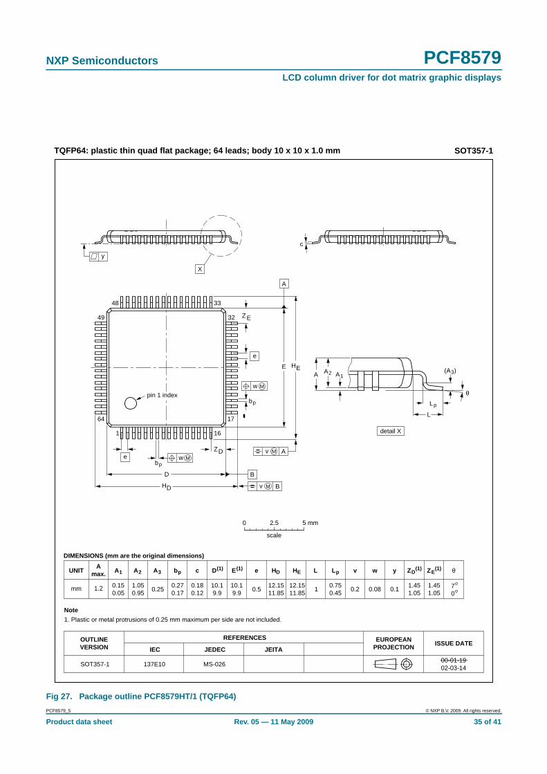
Fig 27. Package outline PCF8579HT/1 (TQFP64)
UNITA
max. A1 A2 A3 bp c E(1) e HE L L p Zywv θ
REFERENCESOUTLINEVERSION
EUROPEANPROJECTION ISSUE DATE
IEC JEDEC JEITA
mm 1.2 0.150.05
1.050.95
0.250.270.17
0.180.12
10.19.9
0.512.1511.85
1.451.05
70
o
o0.08 0.11 0.2
DIMENSIONS (mm are the original dimensions)
Note
1. Plastic or metal protrusions of 0.25 mm maximum per side are not included.
0.750.45
SOT357-1 137E10 MS-02600-01-1902-03-14
D(1) (1)(1)
10.19.9
HD
12.1511.85
EZ
1.451.05
D
bpe
θ
EA1A
Lp
detail X
L
(A )3
B
16
c
DH
bp
EHA2
v M B
D
ZD
A
ZE
e
v M A
X
1
64
49
48 33
32
17
y
pin 1 index
w M
w M
0 2.5 5 mm
scale
TQFP64: plastic thin quad flat package; 64 leads; body 10 x 10 x 1.0 mm SOT357-1
PCF8579_5 © NXP B.V. 2009. All rights reserved.
Product data sheet Rev. 05 — 11 May 2009 35 of 41
NXP Semiconductors PCF8579LCD column driver for dot matrix graphic displays
14. Soldering of SMD packages
This text provides a very brief insight into a complex technology. A more in-depth accountof soldering ICs can be found in Application Note AN10365 “Surface mount reflowsoldering description”.
14.1 Introduction to solderingSoldering is one of the most common methods through which packages are attached toPrinted Circuit Boards (PCBs), to form electrical circuits. The soldered joint provides boththe mechanical and the electrical connection. There is no single soldering method that isideal for all IC packages. Wave soldering is often preferred when through-hole andSurface Mount Devices (SMDs) are mixed on one printed wiring board; however, it is notsuitable for fine pitch SMDs. Reflow soldering is ideal for the small pitches and highdensities that come with increased miniaturization.
14.2 Wave and reflow solderingWave soldering is a joining technology in which the joints are made by solder coming froma standing wave of liquid solder. The wave soldering process is suitable for the following:
• Through-hole components
• Leaded or leadless SMDs, which are glued to the surface of the printed circuit board
Not all SMDs can be wave soldered. Packages with solder balls, and some leadlesspackages which have solder lands underneath the body, cannot be wave soldered. Also,leaded SMDs with leads having a pitch smaller than ~0.6 mm cannot be wave soldered,due to an increased probability of bridging.
The reflow soldering process involves applying solder paste to a board, followed bycomponent placement and exposure to a temperature profile. Leaded packages,packages with solder balls, and leadless packages are all reflow solderable.
Key characteristics in both wave and reflow soldering are:
• Board specifications, including the board finish, solder masks and vias
• Package footprints, including solder thieves and orientation
• The moisture sensitivity level of the packages
• Package placement
• Inspection and repair
• Lead-free soldering versus SnPb soldering
14.3 Wave solderingKey characteristics in wave soldering are:
• Process issues, such as application of adhesive and flux, clinching of leads, boardtransport, the solder wave parameters, and the time during which components areexposed to the wave
• Solder bath specifications, including temperature and impurities
PCF8579_5 © NXP B.V. 2009. All rights reserved.
Product data sheet Rev. 05 — 11 May 2009 36 of 41
NXP Semiconductors PCF8579LCD column driver for dot matrix graphic displays
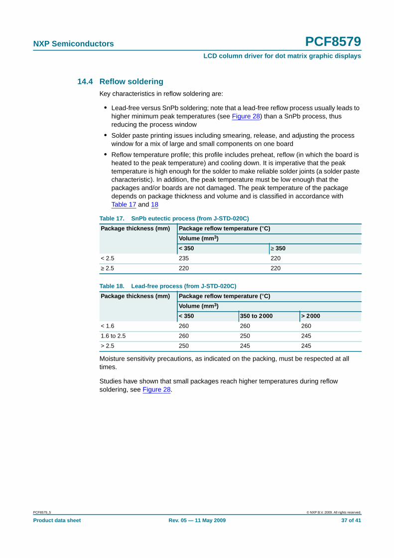
14.4 Reflow solderingKey characteristics in reflow soldering are:
• Lead-free versus SnPb soldering; note that a lead-free reflow process usually leads tohigher minimum peak temperatures (see Figure 28) than a SnPb process, thusreducing the process window
• Solder paste printing issues including smearing, release, and adjusting the processwindow for a mix of large and small components on one board
• Reflow temperature profile; this profile includes preheat, reflow (in which the board isheated to the peak temperature) and cooling down. It is imperative that the peaktemperature is high enough for the solder to make reliable solder joints (a solder pastecharacteristic). In addition, the peak temperature must be low enough that thepackages and/or boards are not damaged. The peak temperature of the packagedepends on package thickness and volume and is classified in accordance withTable 17 and 18
Moisture sensitivity precautions, as indicated on the packing, must be respected at alltimes.
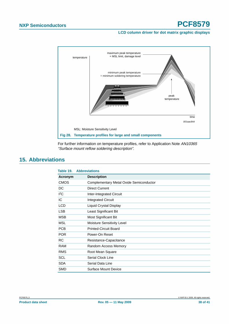
Studies have shown that small packages reach higher temperatures during reflowsoldering, see Figure 28.
Table 17. SnPb eutectic process (from J-STD-020C)
Package thickness (mm) Package reflow temperature ( °C)
Volume (mm 3)
< 350 ≥ 350
< 2.5 235 220
≥ 2.5 220 220
Table 18. Lead-free process (from J-STD-020C)
Package thickness (mm) Package reflow temperature ( °C)
Volume (mm 3)
< 350 350 to 2000 > 2000
< 1.6 260 260 260
1.6 to 2.5 260 250 245
> 2.5 250 245 245
PCF8579_5 © NXP B.V. 2009. All rights reserved.
Product data sheet Rev. 05 — 11 May 2009 37 of 41
NXP Semiconductors PCF8579LCD column driver for dot matrix graphic displays
For further information on temperature profiles, refer to Application Note AN10365“Surface mount reflow soldering description”.
15. Abbreviations
MSL: Moisture Sensitivity Level
Fig 28. Temperature profiles for large and small components
001aac844
temperature
time
minimum peak temperature= minimum soldering temperature
maximum peak temperature= MSL limit, damage level
peak temperature
Table 19. Abbreviations
Acronym Description
CMOS Complementary Metal Oxide Semiconductor
DC Direct Current
I2C Inter-Integrated Circuit
IC Integrated Circuit
LCD Liquid Crystal Display
LSB Least Significant Bit
MSB Most Significant Bit
MSL Moisture Sensitivity Level
PCB Printed-Circuit Board
POR Power-On Reset
RC Resistance-Capacitance
RAM Random Access Memory
RMS Root Mean Square
SCL Serial Clock Line
SDA Serial Data Line
SMD Surface Mount Device
PCF8579_5 © NXP B.V. 2009. All rights reserved.
Product data sheet Rev. 05 — 11 May 2009 38 of 41
NXP Semiconductors PCF8579LCD column driver for dot matrix graphic displays
16. Revision history
Table 20. Revision history
Document ID Release date Data sheet status Change notice Supersedes
PCF8579_5 20090511 Product data sheet - PCF8579_4
Modifications: • The format of this data sheet has been redesigned to comply with the new identityguidelines of NXP Semiconductors.
• Legal texts have been adapted to the new company name where appropriate.
• Added package type TQFP64
• Removed bare die types
• Rearranged information in data sheet
• Changed letter symbols to NXP approved symbols
• Added RAM addressing scheme (Figure 15)
• Added addressing example (Table 16)
PCF8579_4 20030901 Product data sheet - PCF8579_3
PCF8579_3 19970401 Product data sheet - PCF8579_2
PCF8579_2 19961025 Product data sheet - PCF8579_1
PCF8579_1 19940125 Product data sheet - -
PCF8579_5 © NXP B.V. 2009. All rights reserved.
Product data sheet Rev. 05 — 11 May 2009 39 of 41
NXP Semiconductors PCF8579LCD column driver for dot matrix graphic displays
17. Legal information
17.1 Data sheet status
[1] Please consult the most recently issued document before initiating or completing a design.
[2] The term ‘short data sheet’ is explained in section “Definitions”.
[3] The product status of device(s) described in this document may have changed since this document was published and may differ in case of multiple devices. The latest product statusinformation is available on the Internet at URL http://www.nxp.com.
17.2 Definitions
Draft — The document is a draft version only. The content is still underinternal review and subject to formal approval, which may result inmodifications or additions. NXP Semiconductors does not give anyrepresentations or warranties as to the accuracy or completeness ofinformation included herein and shall have no liability for the consequences ofuse of such information.
Short data sheet — A short data sheet is an extract from a full data sheetwith the same product type number(s) and title. A short data sheet is intendedfor quick reference only and should not be relied upon to contain detailed andfull information. For detailed and full information see the relevant full datasheet, which is available on request via the local NXP Semiconductors salesoffice. In case of any inconsistency or conflict with the short data sheet, thefull data sheet shall prevail.
17.3 Disclaimers
General — Information in this document is believed to be accurate andreliable. However, NXP Semiconductors does not give any representations orwarranties, expressed or implied, as to the accuracy or completeness of suchinformation and shall have no liability for the consequences of use of suchinformation.
Right to make changes — NXP Semiconductors reserves the right to makechanges to information published in this document, including withoutlimitation specifications and product descriptions, at any time and withoutnotice. This document supersedes and replaces all information supplied priorto the publication hereof.
Suitability for use — NXP Semiconductors products are not designed,authorized or warranted to be suitable for use in medical, military, aircraft,space or life support equipment, nor in applications where failure ormalfunction of an NXP Semiconductors product can reasonably be expectedto result in personal injury, death or severe property or environmental
damage. NXP Semiconductors accepts no liability for inclusion and/or use ofNXP Semiconductors products in such equipment or applications andtherefore such inclusion and/or use is at the customer’s own risk.
Applications — Applications that are described herein for any of theseproducts are for illustrative purposes only. NXP Semiconductors makes norepresentation or warranty that such applications will be suitable for thespecified use without further testing or modification.
Limiting values — Stress above one or more limiting values (as defined inthe Absolute Maximum Ratings System of IEC 60134) may cause permanentdamage to the device. Limiting values are stress ratings only and operation ofthe device at these or any other conditions above those given in theCharacteristics sections of this document is not implied. Exposure to limitingvalues for extended periods may affect device reliability.
Terms and conditions of sale — NXP Semiconductors products are soldsubject to the general terms and conditions of commercial sale, as publishedat http://www.nxp.com/profile/terms, including those pertaining to warranty,intellectual property rights infringement and limitation of liability, unlessexplicitly otherwise agreed to in writing by NXP Semiconductors. In case ofany inconsistency or conflict between information in this document and suchterms and conditions, the latter will prevail.
No offer to sell or license — Nothing in this document may be interpretedor construed as an offer to sell products that is open for acceptance or thegrant, conveyance or implication of any license under any copyrights, patentsor other industrial or intellectual property rights.
Export control — This document as well as the item(s) described hereinmay be subject to export control regulations. Export might require a priorauthorization from national authorities.
17.4 TrademarksNotice: All referenced brands, product names, service names and trademarksare the property of their respective owners.
I2C-bus — logo is a trademark of NXP B.V.
18. Contact information
For more information, please visit: http://www .nxp.com
For sales office addresses, please send an email to: salesad [email protected]
Document status [1] [2] Product status [3] Definition
Objective [short] data sheet Development This document contains data from the objective specification for product development.
Preliminary [short] data sheet Qualification This document contains data from the preliminary specification.
Product [short] data sheet Production This document contains the product specification.
PCF8579_5 © NXP B.V. 2009. All rights reserved.
Product data sheet Rev. 05 — 11 May 2009 40 of 41
NXP Semiconductors PCF8579LCD column driver for dot matrix graphic displays
19. Contents
1 General description . . . . . . . . . . . . . . . . . . . . . . 12 Features . . . . . . . . . . . . . . . . . . . . . . . . . . . . . . . 13 Applications . . . . . . . . . . . . . . . . . . . . . . . . . . . . 24 Ordering information . . . . . . . . . . . . . . . . . . . . . 25 Marking . . . . . . . . . . . . . . . . . . . . . . . . . . . . . . . . 26 Block diagram . . . . . . . . . . . . . . . . . . . . . . . . . . 37 Pinning information . . . . . . . . . . . . . . . . . . . . . . 47.1 Pinning . . . . . . . . . . . . . . . . . . . . . . . . . . . . . . . 47.2 Pin description . . . . . . . . . . . . . . . . . . . . . . . . . 78 Functional description . . . . . . . . . . . . . . . . . . . 78.1 Power-on reset . . . . . . . . . . . . . . . . . . . . . . . . . 78.2 Multiplexed LCD bias generation . . . . . . . . . . . 88.3 LCD drive mode waveforms . . . . . . . . . . . . . . 108.4 Timing generator. . . . . . . . . . . . . . . . . . . . . . . 138.5 Column drivers . . . . . . . . . . . . . . . . . . . . . . . . 138.6 Characteristics of the I2C-bus. . . . . . . . . . . . . 138.6.1 Bit transfer . . . . . . . . . . . . . . . . . . . . . . . . . . . 138.6.2 START and STOP conditions . . . . . . . . . . . . . 138.6.3 System configuration . . . . . . . . . . . . . . . . . . . 138.6.4 Acknowledge . . . . . . . . . . . . . . . . . . . . . . . . . 138.6.5 I2C-bus controller . . . . . . . . . . . . . . . . . . . . . . 158.6.6 Input filters . . . . . . . . . . . . . . . . . . . . . . . . . . . 158.6.7 I2C-bus protocol . . . . . . . . . . . . . . . . . . . . . . . 158.7 Display RAM . . . . . . . . . . . . . . . . . . . . . . . . . . 178.7.1 Data pointer . . . . . . . . . . . . . . . . . . . . . . . . . . 178.7.2 Subaddress counter . . . . . . . . . . . . . . . . . . . . 178.8 Command decoder . . . . . . . . . . . . . . . . . . . . . 178.9 RAM access . . . . . . . . . . . . . . . . . . . . . . . . . . 208.9.1 Display control . . . . . . . . . . . . . . . . . . . . . . . . 239 Limiting values. . . . . . . . . . . . . . . . . . . . . . . . . 2410 Static characteristics. . . . . . . . . . . . . . . . . . . . 2511 Dynamic characteristics . . . . . . . . . . . . . . . . . 2612 Application information. . . . . . . . . . . . . . . . . . 2813 Package outline . . . . . . . . . . . . . . . . . . . . . . . . 3314 Soldering of SMD packages . . . . . . . . . . . . . . 3614.1 Introduction to soldering . . . . . . . . . . . . . . . . . 3614.2 Wave and reflow soldering . . . . . . . . . . . . . . . 3614.3 Wave soldering . . . . . . . . . . . . . . . . . . . . . . . . 3614.4 Reflow soldering . . . . . . . . . . . . . . . . . . . . . . . 3715 Abbreviations . . . . . . . . . . . . . . . . . . . . . . . . . . 3816 Revision history . . . . . . . . . . . . . . . . . . . . . . . . 3917 Legal information. . . . . . . . . . . . . . . . . . . . . . . 4017.1 Data sheet status . . . . . . . . . . . . . . . . . . . . . . 4017.2 Definitions . . . . . . . . . . . . . . . . . . . . . . . . . . . . 4017.3 Disclaimers . . . . . . . . . . . . . . . . . . . . . . . . . . . 40
17.4 Trademarks . . . . . . . . . . . . . . . . . . . . . . . . . . 4018 Contact information . . . . . . . . . . . . . . . . . . . . 4019 Contents. . . . . . . . . . . . . . . . . . . . . . . . . . . . . . 41
© NXP B.V. 2009. All rights reserved.For more information, please visit: http://www.nxp.comFor sales office addresses, please send an email to: [email protected]
Date of release: 11 May 2009
Document identifier: PCF8579_5
Please be aware that important notices concerning this document and the product(s)described herein, have been included in section ‘Legal information’.