PCA9685 16-channel, 12-bit PWM Fm+ I2C-bus LED...
50
1. General description The PCA9685 is an I 2 C-bus controlled 16-channel LED controller optimized for LCD Red/Green/Blue/Amber (RGBA) color backlighting applications. Each LED output has its own 12-bit resolution (4096 steps) fixed frequency individual PWM controller that operates at a programmable frequency from a typical of 40 Hz to 1000 Hz with a duty cycle that is adjustable from 0 % to 100 % to allow the LED to be set to a specific brightness value. All outputs are set to the same PWM frequency. Each LED output can be off or on (no PWM control), or set at its individual PWM controller value. The LED output driver is programmed to be either open-drain with a 25 mA current sink capability at 5 V or totem pole with a 25 mA sink, 10 mA source capability at 5 V. The PCA9685 operates with a supply voltage range of 2.3 V to 5.5 V and the inputs and outputs are 5.5 V tolerant. LEDs can be directly connected to the LED output (up to 25 mA, 5.5 V) or controlled with external drivers and a minimum amount of discrete components for larger current or higher voltage LEDs. The PCA9685 is in the new Fast-mode Plus (Fm+) family. Fm+ devices offer higher frequency (up to 1 MHz) and more densely populated bus operation (up to 4000 pF). Although the PCA9635 and PCA9685 have many similar features, the PCA9685 has some unique features that make it more suitable for applications such as LCD backlighting and Ambilight: • The PCA9685 allows staggered LED output on and off times to minimize current surges. The on and off time delay is independently programmable for each of the 16 channels. This feature is not available in PCA9635. • The PCA9685 has 4096 steps (12-bit PWM) of individual LED brightness control. The PCA9635 has only 256 steps (8-bit PWM). • When multiple LED controllers are incorporated in a system, the PWM pulse widths between multiple devices may differ if PCA9635s are used. The PCA9685 has a programmable prescaler to adjust the PWM pulse widths of multiple devices. • The PCA9685 has an external clock input pin that will accept user-supplied clock (50 MHz max.) in place of the internal 25 MHz oscillator. This feature allows synchronization of multiple devices. The PCA9635 does not have external clock input feature. • Like the PCA9635, PCA9685 also has a built-in oscillator for the PWM control. However, the frequency used for PWM control in the PCA9685 is adjustable from about 40 Hz to 1000 Hz as compared to the typical 97.6 kHz frequency of the PCA9635. This allows the use of PCA9685 with external power supply controllers. All bits are set at the same frequency. • The Power-On Reset (POR) default state of LEDn output pins is LOW in the case of PCA9685. It is HIGH for PCA9635. PCA9685 16-channel, 12-bit PWM Fm+ I 2 C-bus LED controller Rev. 02 — 16 July 2009 Product data sheet
Transcript of PCA9685 16-channel, 12-bit PWM Fm+ I2C-bus LED...

1. General description
The PCA9685 is an I2C-bus controlled 16-channel LED controller optimized for LCDRed/Green/Blue/Amber (RGBA) color backlighting applications. Each LED output has itsown 12-bit resolution (4096 steps) fixed frequency individual PWM controller that operatesat a programmable frequency from a typical of 40 Hz to 1000 Hz with a duty cycle that isadjustable from 0 % to 100 % to allow the LED to be set to a specific brightness value.All outputs are set to the same PWM frequency.
Each LED output can be off or on (no PWM control), or set at its individual PWM controllervalue. The LED output driver is programmed to be either open-drain with a 25 mA currentsink capability at 5 V or totem pole with a 25 mA sink, 10 mA source capability at 5 V. ThePCA9685 operates with a supply voltage range of 2.3 V to 5.5 V and the inputs andoutputs are 5.5 V tolerant. LEDs can be directly connected to the LED output (up to25 mA, 5.5 V) or controlled with external drivers and a minimum amount of discretecomponents for larger current or higher voltage LEDs.
The PCA9685 is in the new Fast-mode Plus (Fm+) family. Fm+ devices offer higherfrequency (up to 1 MHz) and more densely populated bus operation (up to 4000 pF).
Although the PCA9635 and PCA9685 have many similar features, the PCA9685 hassome unique features that make it more suitable for applications such as LCD backlightingand Ambilight:
• The PCA9685 allows staggered LED output on and off times to minimize currentsurges. The on and off time delay is independently programmable for each of the16 channels. This feature is not available in PCA9635.
• The PCA9685 has 4096 steps (12-bit PWM) of individual LED brightness control. ThePCA9635 has only 256 steps (8-bit PWM).
• When multiple LED controllers are incorporated in a system, the PWM pulse widthsbetween multiple devices may differ if PCA9635s are used. The PCA9685 has aprogrammable prescaler to adjust the PWM pulse widths of multiple devices.
• The PCA9685 has an external clock input pin that will accept user-supplied clock(50 MHz max.) in place of the internal 25 MHz oscillator. This feature allowssynchronization of multiple devices. The PCA9635 does not have external clock inputfeature.
• Like the PCA9635, PCA9685 also has a built-in oscillator for the PWM control.However, the frequency used for PWM control in the PCA9685 is adjustable fromabout 40 Hz to 1000 Hz as compared to the typical 97.6 kHz frequency of thePCA9635. This allows the use of PCA9685 with external power supply controllers. Allbits are set at the same frequency.
• The Power-On Reset (POR) default state of LEDn output pins is LOW in the case ofPCA9685. It is HIGH for PCA9635.
PCA968516-channel, 12-bit PWM Fm+ I 2C-bus LED controllerRev. 02 — 16 July 2009 Product data sheet

NXP Semiconductors PCA968516-channel, 12-bit PWM Fm+ I 2C-bus LED controller
The active LOW Output Enable input pin (OE) allows asynchronous control of the LEDoutputs and can be used to set all the outputs to a defined I2C-bus programmable logicstate. The OE can also be used to externally ‘pulse width modulate’ the outputs, which isuseful when multiple devices need to be dimmed or blinked together using softwarecontrol.
Software programmable LED All Call and three Sub Call I2C-bus addresses allow all ordefined groups of PCA9685 devices to respond to a common I2C-bus address, allowingfor example, all red LEDs to be turned on or off at the same time or marquee chasingeffect, thus minimizing I2C-bus commands. Six hardware address pins allow up to62 devices on the same bus.
The Software Reset (SWRST) General Call allows the master to perform a reset of thePCA9685 through the I2C-bus, identical to the Power-On Reset (POR) that initializes theregisters to their default state causing the outputs to be set LOW. This allows an easy andquick way to reconfigure all device registers to the same condition via software.
2. Features
n 16 LED drivers. Each output programmable at:
u Off
u On
u Programmable LED brightness
u Programmable LED turn-on time to help reduce EMI
n 1 MHz Fast-mode Plus compatible I2C-bus interface with 30 mA high drive capabilityon SDA output for driving high capacitive buses
n 4096-step (12-bit) linear programmable brightness per LED output varying from fullyoff (default) to maximum brightness
n LED output frequency (all LEDs) typically varies from 40 Hz to 1000 Hz (Default of 1Ehin PRE_SCALE register results in a 200 Hz refresh rate with oscillator clock of25 MHz.)
n Sixteen totem pole outputs (sink 25 mA and source 10 mA at 5 V) with softwareprogrammable open-drain LED outputs selection (default at totem pole). No inputfunction.
n Output state change programmable on the Acknowledge or the STOP Command toupdate outputs byte-by-byte or all at the same time (default to ‘Change on STOP’).
n Active LOW Output Enable (OE) input pin. LEDn outputs programmable to logic 1,logic 0 (default at power-up) or ‘high-impedance’ when OE is HIGH.
n 6 hardware address pins allow 62 PCA9685 devices to be connected to the sameI2C-bus
n Toggling OE allows for hardware LED blinking
n 4 software programmable I2C-bus addresses (one LED All Call address and three LEDSub Call addresses) allow groups of devices to be addressed at the same time in anycombination (for example, one register used for ‘All Call’ so that all the PCA9685s onthe I2C-bus can be addressed at the same time and the second register used for threedifferent addresses so that 1⁄3 of all devices on the bus can be addressed at the sametime in a group). Software enable and disable for these I2C-bus address.
n Software Reset feature (SWRST General Call) allows the device to be reset throughthe I2C-bus
PCA9685_2 © NXP B.V. 2009. All rights reserved.
Product data sheet Rev. 02 — 16 July 2009 2 of 50

NXP Semiconductors PCA968516-channel, 12-bit PWM Fm+ I 2C-bus LED controller
n 25 MHz typical internal oscillator requires no external components
n External 50 MHz (max.) clock input
n Internal power-on reset
n Noise filter on SDA/SCL inputs
n Edge rate control on outputs
n No output glitches on power-up
n Supports hot insertion
n Low standby current
n Operating power supply voltage range of 2.3 V to 5.5 V
n 5.5 V tolerant inputs
n −40 °C to +85 °C operation
n ESD protection exceeds 2000 V HBM per JESD22-A114, 200 V MM perJESD22-A115 and 1000 V CDM per JESD22-C101
n Latch-up testing is done to JEDEC Standard JESD78 which exceeds 100 mA
n Packages offered: TSSOP28, HVQFN28
3. Applications
n RGB or RGBA LED drivers
n LED status information
n LED displays
n LCD backlights
n Keypad backlights for cellular phones or handheld devices
4. Ordering information
[1] PCA9685PW/Q900 is AEC-Q100 compliant. Contact [email protected] for PPAP.
Table 1. Ordering information
Type number Topside mark Package
Name Description Version
PCA9685PW PCA9685PW TSSOP28 plastic thin shrink small outline package;28 leads; body width 4.4 mm
SOT361-1
PCA9685PW/Q900[1] PCA9685PW TSSOP28 plastic thin shrink small outline package;28 leads; body width 4.4 mm
SOT361-1
PCA9685BS PCA9685BS HVQFN28 plastic thermal enhanced very thin quad flatpackage; no leads; 28 terminals;body 6 × 6 × 0.85 mm
SOT788-1
PCA9685_2 © NXP B.V. 2009. All rights reserved.
Product data sheet Rev. 02 — 16 July 2009 3 of 50

NXP Semiconductors PCA968516-channel, 12-bit PWM Fm+ I 2C-bus LED controller
5. Block diagram
Remark: Only one LED output shown for clarity.
Fig 1. Block diagram of PCA9685
A0 A1 A2 A3 A4 A5
002aac824
I2C-BUSCONTROL
INPUT FILTER
PCA9685
POWER-ONRESET
SCL
SDA
VDD
VSSLED
STATESELECT
REGISTER
PWMREGISTER XBRIGHTNESS
CONTROL
MUX/CONTROL
OE
'0' – permanently OFF'1' – permanently ON
VDD
LEDnPRESCALE
25 MHzOSCILLATOR CLOCK
SWITCHEXTCLK
PCA9685_2 © NXP B.V. 2009. All rights reserved.
Product data sheet Rev. 02 — 16 July 2009 4 of 50

NXP Semiconductors PCA968516-channel, 12-bit PWM Fm+ I 2C-bus LED controller
6. Pinning information
6.1 Pinning
6.2 Pin description
Fig 2. Pin configuration for TSSOP28 Fig 3. Pin configuration for HVQFN28
PCA9685PWPCA9685PW/Q900
A0 VDD
A1 SDA
A2 SCL
A3 EXTCLK
A4 A5
LED0 OE
LED1 LED15
LED2 LED14
LED3 LED13
LED4 LED12
LED5 LED11
LED6 LED10
LED7 LED9
VSS LED8
002aac825
1
2
3
4
5
6
7
8
9
10
11
12
13
14
16
15
18
17
20
19
22
21
24
23
26
25
28
27
002aad236
PCA9685BS
LED11
LED3
LED4
LED12
LED2 LED13
LED1 LED14
LED0 LED15
A4 OE
A3 A5
LED
5
LED
6
LED
7
VS
S
LED
8
LED
9
LED
10
A2
A1
A0
VD
D
SD
A
SC
L
EX
TC
LK
Transparent top view
7 15
6 16
5 17
4 18
3 19
2 20
1 21
8 9 10 11 12 13 14
28 27 26 25 24 23 22
terminal 1index area
Table 2. Pin description
Symbol Pin Type Description
TSSOP28 HVQFN28
A0 1 26 I address input 0
A1 2 27 I address input 1
A2 3 28 I address input 2
A3 4 1 I address input 3
A4 5 2 I address input 4
LED0 6 3 O LED driver 0
LED1 7 4 O LED driver 1
LED2 8 5 O LED driver 2
LED3 9 6 O LED driver 3
LED4 10 7 O LED driver 4
LED5 11 8 O LED driver 5
LED6 12 9 O LED driver 6
LED7 13 10 O LED driver 7
VSS 14 11[1] power supply supply ground
LED8 15 12 O LED driver 8
LED9 16 13 O LED driver 9
LED10 17 14 O LED driver 10
LED11 18 15 O LED driver 11
PCA9685_2 © NXP B.V. 2009. All rights reserved.
Product data sheet Rev. 02 — 16 July 2009 5 of 50

NXP Semiconductors PCA968516-channel, 12-bit PWM Fm+ I 2C-bus LED controller
[1] HVQFN28 package die supply ground is connected to both VSS pin and exposed center pad. VSS pin mustbe connected to supply ground for proper device operation. For enhanced thermal, electrical, and boardlevel performance, the exposed pad needs to be soldered to the board using a corresponding thermal padon the board and for proper heat conduction through the board, thermal vias need to be incorporated in thePCB in the thermal pad region.
[2] This pin must be grounded when this feature is not used.
7. Functional description
Refer to Figure 1 “Block diagram of PCA9685”.
7.1 Device addressesFollowing a START condition, the bus master must output the address of the slave it isaccessing.
There are a maximum of 64 possible programmable addresses using the 6 hardwareaddress pins. Two of these addresses, Software Reset and LED All Call, cannot be usedbecause their default power-up state is ON, leaving a maximum of 62 addresses. Usingother reserved addresses, as well as any other subcall address, will reduce the totalnumber of possible addresses even further.
7.1.1 Regular I 2C-bus slave address
The I2C-bus slave address of the PCA9685 is shown in Figure 4. To conserve power, nointernal pull-up resistors are incorporated on the hardware selectable address pins andthey must be pulled HIGH or LOW.
Remark: Using reserved I2C-bus addresses will interfere with other devices, but only if thedevices are on the bus and/or the bus will be open to other I2C-bus systems at some laterdate. In a closed system where the designer controls the address assignment theseaddresses can be used since the PCA9685 treats them like any other address. TheLED All Call, Software Reset and PCA9564 or PCA9665 slave address (if on the bus) cannever be used for individual device addresses.
• PCA9685 LED All Call address (1110 000) and Software Reset (0000 0110) whichare active on start-up
LED12 19 16 O LED driver 12
LED13 20 17 O LED driver 13
LED14 21 18 O LED driver 14
LED15 22 19 O LED driver 15
OE 23 20 I active LOW output enable
A5 24 21 I address input 5
EXTCLK 25 22 I external clock input[2]
SCL 26 23 I serial clock line
SDA 27 24 I/O serial data line
VDD 28 25 power supply supply voltage
Table 2. Pin description …continued
Symbol Pin Type Description
TSSOP28 HVQFN28
PCA9685_2 © NXP B.V. 2009. All rights reserved.
Product data sheet Rev. 02 — 16 July 2009 6 of 50

NXP Semiconductors PCA968516-channel, 12-bit PWM Fm+ I 2C-bus LED controller
• PCA9564 (0000 000) or PCA9665 (1110 000) slave address which is active onstart-up
• ‘reserved for future use’ I2C-bus addresses (0000 011, 1111 1XX)
• slave devices that use the 10-bit addressing scheme (1111 0XX)
• slave devices that are designed to respond to the General Call address (0000 000)which is used as the software reset address
• High-speed mode (Hs-mode) master code (0000 1XX)
The last bit of the address byte defines the operation to be performed. When set to logic 1a read is selected, while a logic 0 selects a write operation.
7.1.2 LED All Call I 2C-bus address
• Default power-up value (ALLCALLADR register): E0h or 1110 000X
• Programmable through I2C-bus (volatile programming)
• At power-up, LED All Call I2C-bus address is enabled. PCA9685 sends an ACK whenE0h (R/W = 0) or E1h (R/W = 1) is sent by the master.
See Section 7.3.7 “ALLCALLADR, LED All Call I2C-bus address” for more detail.
Remark: The default LED All Call I2C-bus address (E0h or 1110 000X) must not be usedas a regular I2C-bus slave address since this address is enabled at power-up. All thePCA9685s on the I2C-bus will acknowledge the address if sent by the I2C-bus master.
7.1.3 LED Sub Call I 2C-bus addresses
• 3 different I2C-bus addresses can be used
• Default power-up values:
– SUBADR1 register: E2h or 1110 001X
– SUBADR2 register: E4h or 1110 010X
– SUBADR3 register: E8h or 1110 100X
• Programmable through I2C-bus (volatile programming)
• At power-up, Sub Call I2C-bus addresses are disabled. PCA9685 does not send anACK when E2h (R/W = 0) or E3h (R/W = 1), E4h (R/W = 0) or E5h (R/W = 1), orE8h (R/W = 0) or E9h (R/W = 1) is sent by the master.
See Section 7.3.6 “SUBADR1 to SUBADR3, I2C-bus subaddress 1 to 3” for more detail.
Remark: The default LED Sub Call I2C-bus addresses may be used as regular I2C-busslave addresses as long as they are disabled.
Fig 4. Slave address
R/W
002aad168
1 A5 A4 A3 A2 A1 A0
hardware selectable
slave address
fixed
PCA9685_2 © NXP B.V. 2009. All rights reserved.
Product data sheet Rev. 02 — 16 July 2009 7 of 50
NXP Semiconductors PCA968516-channel, 12-bit PWM Fm+ I 2C-bus LED controller
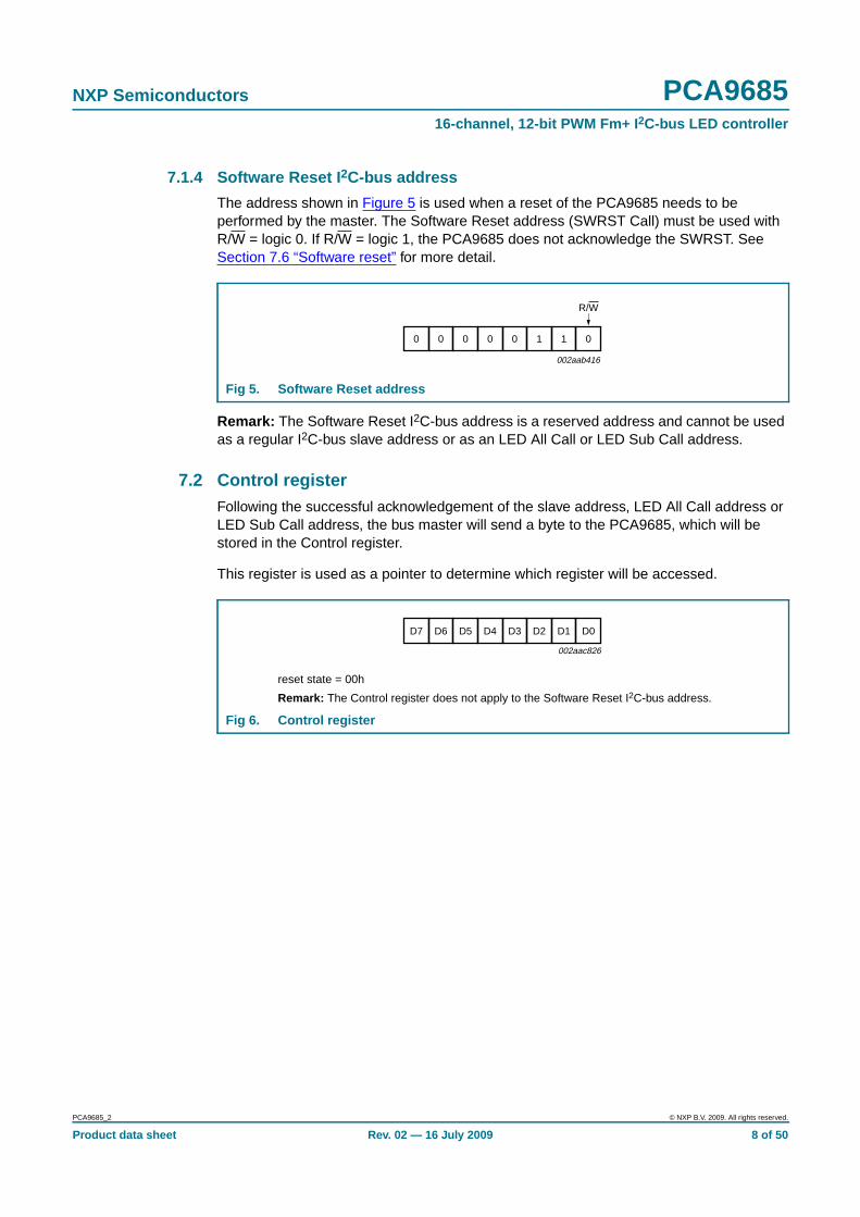
7.1.4 Software Reset I 2C-bus address
The address shown in Figure 5 is used when a reset of the PCA9685 needs to beperformed by the master. The Software Reset address (SWRST Call) must be used withR/W = logic 0. If R/W = logic 1, the PCA9685 does not acknowledge the SWRST. SeeSection 7.6 “Software reset” for more detail.
Remark: The Software Reset I2C-bus address is a reserved address and cannot be usedas a regular I2C-bus slave address or as an LED All Call or LED Sub Call address.
7.2 Control registerFollowing the successful acknowledgement of the slave address, LED All Call address orLED Sub Call address, the bus master will send a byte to the PCA9685, which will bestored in the Control register.
This register is used as a pointer to determine which register will be accessed.
Fig 5. Software Reset address
0
002aab416
0 0 0 0 0 1 1
R/W
reset state = 00h
Remark: The Control register does not apply to the Software Reset I2C-bus address.
Fig 6. Control register
002aac826
D7 D6 D5 D4 D3 D2 D1 D0
PCA9685_2 © NXP B.V. 2009. All rights reserved.
Product data sheet Rev. 02 — 16 July 2009 8 of 50

NXP Semiconductors PCA968516-channel, 12-bit PWM Fm+ I 2C-bus LED controller
7.3 Register definitions
Table 3. Register summary
Register#(decimal)
Register# (hex)
D7 D6 D5 D4 D3 D2 D1 D0 Name Type Function
0 00 0 0 0 0 0 0 0 0 MODE1 read/write Mode register 1
1 01 0 0 0 0 0 0 0 1 MODE2 read/write Mode register 2
2 02 0 0 0 0 0 0 1 0 SUBADR1 read/write I2C-bus subaddress 1
3 03 0 0 0 0 0 0 1 1 SUBADR2 read/write I2C-bus subaddress 2
4 04 0 0 0 0 0 1 0 0 SUBADR3 read/write I2C-bus subaddress 3
5 05 0 0 0 0 0 1 0 1 ALLCALLADR read/write LED All Call I2C-busaddress
6 06 0 0 0 0 0 1 1 0 LED0_ON_L read/write LED0 output andbrightness control byte 0
7 07 0 0 0 0 0 1 1 1 LED0_ON_H read/write LED0 output andbrightness control byte 1
8 08 0 0 0 0 1 0 0 0 LED0_OFF_L read/write LED0 output andbrightness control byte 2
9 09 0 0 0 0 1 0 0 1 LED0_OFF_H read/write LED0 output andbrightness control byte 3
10 0A 0 0 0 0 1 0 1 0 LED1_ON_L read/write LED1 output andbrightness control byte 0
11 0B 0 0 0 0 1 0 1 1 LED1_ON_H read/write LED1 output andbrightness control byte 1
12 0C 0 0 0 0 1 1 0 0 LED1_OFF_L read/write LED1 output andbrightness control byte 2
13 0D 0 0 0 0 1 1 0 1 LED1_OFF_H read/write LED1 output andbrightness control byte 3
14 0E 0 0 0 0 1 1 1 0 LED2_ON_L read/write LED2 output andbrightness control byte 0
15 0F 0 0 0 0 1 1 1 1 LED2_ON_H read/write LED2 output andbrightness control byte 1
16 10 0 0 0 1 0 0 0 0 LED2_OFF_L read/write LED2 output andbrightness control byte 2
17 11 0 0 0 1 0 0 0 1 LED2_OFF_H read/write LED2 output andbrightness control byte 3
18 12 0 0 0 1 0 0 1 0 LED3_ON_L read/write LED3 output andbrightness control byte 0
19 13 0 0 0 1 0 0 1 1 LED3_ON_H read/write LED3 output andbrightness control byte 1
20 14 0 0 0 1 0 1 0 0 LED3_OFF_L read/write LED3 output andbrightness control byte 2
21 15 0 0 0 1 0 1 0 1 LED3_OFF_H read/write LED3 output andbrightness control byte 3
PCA9685_2 © NXP B.V. 2009. All rights reserved.
Product data sheet Rev. 02 — 16 July 2009 9 of 50

NXP Semiconductors PCA968516-channel, 12-bit PWM Fm+ I 2C-bus LED controller
22 16 0 0 0 1 0 1 1 0 LED4_ON_L read/write LED4 output andbrightness control byte 0
23 17 0 0 0 1 0 1 1 1 LED4_ON_H read/write LED4 output andbrightness control byte 1
24 18 0 0 0 1 1 0 0 0 LED4_OFF_L read/write LED4 output andbrightness control byte 2
25 19 0 0 0 1 1 0 0 1 LED4_OFF_H read/write LED4 output andbrightness control byte 3
26 1A 0 0 0 1 1 0 1 0 LED5_ON_L read/write LED5 output andbrightness control byte 0
27 1B 0 0 0 1 1 0 1 1 LED5_ON_H read/write LED5 output andbrightness control byte 1
28 1C 0 0 0 1 1 1 0 0 LED5_OFF_L read/write LED5 output andbrightness control byte 2
29 1D 0 0 0 1 1 1 0 1 LED5_OFF_H read/write LED5 output andbrightness control byte 3
30 1E 0 0 0 1 1 1 1 0 LED6_ON_L read/write LED6 output andbrightness control byte 0
31 1F 0 0 0 1 1 1 1 1 LED6_ON_H read/write LED6 output andbrightness control byte 1
32 20 0 0 1 0 0 0 0 0 LED6_OFF_L read/write LED6 output andbrightness control byte 2
33 21 0 0 1 0 0 0 0 1 LED6_OFF_H read/write LED6 output andbrightness control byte 3
34 22 0 0 1 0 0 0 1 0 LED7_ON_L read/write LED7 output andbrightness control byte 0
35 23 0 0 1 0 0 0 1 1 LED7_ON_H read/write LED7 output andbrightness control byte 1
36 24 0 0 1 0 0 1 0 0 LED7_OFF_L read/write LED7 output andbrightness control byte 2
37 25 0 0 1 0 0 1 0 1 LED7_OFF_H read/write LED7 output andbrightness control byte 3
38 26 0 0 1 0 0 1 1 0 LED8_ON_L read/write LED8 output andbrightness control byte 0
39 27 0 0 1 0 0 1 1 1 LED8_ON_H read/write LED8 output andbrightness control byte 1
40 28 0 0 1 0 1 0 0 0 LED8_OFF_L read/write LED8 output andbrightness control byte 2
41 29 0 0 1 0 1 0 0 1 LED8_OFF_H read/write LED8 output andbrightness control byte 3
Table 3. Register summary …continued
Register#(decimal)
Register# (hex)
D7 D6 D5 D4 D3 D2 D1 D0 Name Type Function
PCA9685_2 © NXP B.V. 2009. All rights reserved.
Product data sheet Rev. 02 — 16 July 2009 10 of 50

NXP Semiconductors PCA968516-channel, 12-bit PWM Fm+ I 2C-bus LED controller
42 2A 0 0 1 0 1 0 1 0 LED9_ON_L read/write LED9 output andbrightness control byte 0
43 2B 0 0 1 0 1 0 1 1 LED9_ON_H read/write LED9 output andbrightness control byte 1
44 2C 0 0 1 0 1 1 0 0 LED9_OFF_L read/write LED9 output andbrightness control byte 2
45 2D 0 0 1 0 1 1 0 1 LED9_OFF_H read/write LED9 output andbrightness control byte 3
46 2E 0 0 1 0 1 1 1 0 LED10_ON_L read/write LED10 output andbrightness control byte 0
47 2F 0 0 1 0 1 1 1 1 LED10_ON_H read/write LED10 output andbrightness control byte 1
48 30 0 0 1 1 0 0 0 0 LED10_OFF_L read/write LED10 output andbrightness control byte 2
49 31 0 0 1 1 0 0 0 1 LED10_OFF_H read/write LED10 output andbrightness control byte 3
50 32 0 0 1 1 0 0 1 0 LED11_ON_L read/write LED11 output andbrightness control byte 0
51 33 0 0 1 1 0 0 1 1 LED11_ON_H read/write LED11 output andbrightness control byte 1
52 34 0 0 1 1 0 1 0 0 LED11_OFF_L read/write LED11 output andbrightness control byte 2
53 35 0 0 1 1 0 1 0 1 LED11_OFF_H read/write LED11 output andbrightness control byte 3
54 36 0 0 1 1 0 1 1 0 LED12_ON_L read/write LED12 output andbrightness control byte 0
55 37 0 0 1 1 0 1 1 1 LED12_ON_H read/write LED12 output andbrightness control byte 1
56 38 0 0 1 1 1 0 0 0 LED12_OFF_L read/write LED12 output andbrightness control byte 2
57 39 0 0 1 1 1 0 0 1 LED12_OFF_H read/write LED12 output andbrightness control byte 3
58 3A 0 0 1 1 1 0 1 0 LED13_ON_L read/write LED13 output andbrightness control byte 0
59 3B 0 0 1 1 1 0 1 1 LED13_ON_H read/write LED13 output andbrightness control byte 1
60 3C 0 0 1 1 1 1 0 0 LED13_OFF_L read/write LED13 output andbrightness control byte 2
61 3D 0 0 1 1 1 1 0 1 LED13_OFF_H read/write LED13 output andbrightness control byte 3
Table 3. Register summary …continued
Register#(decimal)
Register# (hex)
D7 D6 D5 D4 D3 D2 D1 D0 Name Type Function
PCA9685_2 © NXP B.V. 2009. All rights reserved.
Product data sheet Rev. 02 — 16 July 2009 11 of 50

NXP Semiconductors PCA968516-channel, 12-bit PWM Fm+ I 2C-bus LED controller
[1] Writes to PRE_SCALE register are blocked when SLEEP bit is logic 0 (MODE 1).
[2] Reserved. Writes to this register may cause unpredictable results.
Remark: Auto Increment past register 69 will point to MODE1 register (register 0).Auto Increment also works from register 250 to register 254, then rolls over to register 0.
62 3E 0 0 1 1 1 1 1 0 LED14_ON_L read/write LED14 output andbrightness control byte 0
63 3F 0 0 1 1 1 1 1 1 LED14_ON_H read/write LED14 output andbrightness control byte 1
64 40 0 1 0 0 0 0 0 0 LED14_OFF_L read/write LED14 output andbrightness control byte 2
65 41 0 1 0 0 0 0 0 1 LED14_OFF_H read/write LED14 output andbrightness control byte 3
66 42 0 1 0 0 0 0 1 0 LED15_ON_L read/write LED15 output andbrightness control byte 0
67 43 0 1 0 0 0 0 1 1 LED15_ON_H read/write LED15 output andbrightness control byte 1
68 44 0 1 0 0 0 1 0 0 LED15_OFF_L read/write LED15 output andbrightness control byte 2
69 45 0 1 0 0 0 1 0 1 LED15_OFF_H read/write LED15 output andbrightness control byte 3
... reserved for future use
250 FA 1 1 1 1 1 0 1 0 ALL_LED_ON_L write/readzero
load all the LEDn_ONregisters, byte 0
251 FB 1 1 1 1 1 0 1 1 ALL_LED_ON_H write/readzero
load all the LEDn_ONregisters, byte 1
252 FC 1 1 1 1 1 1 0 0 ALL_LED_OFF_L write/readzero
load all the LEDn_OFFregisters, byte 0
253 FD 1 1 1 1 1 1 0 1 ALL_LED_OFF_H write/readzero
load all the LEDn_OFFregisters, byte 1
254 FE 1 1 1 1 1 1 1 0 PRE_SCALE[1] read/write prescaler for outputfrequency
255 FF 1 1 1 1 1 1 1 1 TestMode[2] read/write defines the test mode tobe entered
... All further addresses are reserved for future use; reserved addresses will not be acknowledged.
Table 3. Register summary …continued
Register#(decimal)
Register# (hex)
D7 D6 D5 D4 D3 D2 D1 D0 Name Type Function
PCA9685_2 © NXP B.V. 2009. All rights reserved.
Product data sheet Rev. 02 — 16 July 2009 12 of 50

NXP Semiconductors PCA968516-channel, 12-bit PWM Fm+ I 2C-bus LED controller
7.3.1 Mode register 1, MODE1
[1] When the Auto Increment flag is set, AI = 1, the Control register is automatically incremented after a read or write. This allows the userto program the registers sequentially.
[2] It takes 500 µs max. for the oscillator to be up and running once SLEEP bit has been set to logic 0. Timings on LEDn outputs are notguaranteed if PWM control registers are accessed within the 500 µs window. There is no start-up delay required when using theEXTCLK pin as the PWM clock.
[3] No PWM control is possible when the oscillator is off.
[4] When the oscillator is off (Sleep mode) the LEDn outputs cannot be turned on, off or dimmed/blinked.
Table 4. MODE1 - Mode register 1 (address 00h) bit descriptionLegend: * default value.
Bit Symbol Access Value Description
7 RESTART R Shows state of RESTART logic. See Section 7.3.1.1 for detail.
W User writes logic 1 to this bit to clear it to logic 0. A user write of logic 0 will have noeffect. See Section 7.3.1.1 for detail.
0* Restart disabled.
1 Restart enabled.
6 EXTCLK R/W To use the EXTCLK pin, this bit must be set by the following sequence:
1. Set the SLEEP bit in MODE1. This turns off the internal oscillator.
2. Write logic 1s to both the SLEEP and EXTCLK bits in MODE1. The switch isnow made. The external clock can be active during the switch because theSLEEP bit is set.
This bit is a ‘sticky bit’, that is, it cannot be cleared by writing a logic 0 to it. TheEXTCLK bit can only be cleared by a power cycle or software reset.
EXTCLK range is DC to 50 MHz.
0* Use internal clock.
1 Use EXTCLK pin clock.
5 AI R/W 0* Register Auto-Increment disabled[1].
1 Register Auto-Increment enabled.
4 SLEEP R/W 0 Normal mode[2].
1* Low power mode. Oscillator off[3][4].
3 SUB1 R/W 0* PCA9685 does not respond to I2C-bus subaddress 1.
1 PCA9685 responds to I2C-bus subaddress 1.
2 SUB2 R/W 0* PCA9685 does not respond to I2C-bus subaddress 2.
1 PCA9685 responds to I2C-bus subaddress 2.
1 SUB3 R/W 0* PCA9685 does not respond to I2C-bus subaddress 3.
1 PCA9685 responds to I2C-bus subaddress 3.
0 ALLCALL R/W 0 PCA9685 does not respond to LED All Call I2C-bus address.
1* PCA9685 responds to LED All Call I2C-bus address.
refresh_rateEXTCLK
4096 prescale 1+( )×-------------------------------------------------------=
PCA9685_2 © NXP B.V. 2009. All rights reserved.
Product data sheet Rev. 02 — 16 July 2009 13 of 50

NXP Semiconductors PCA968516-channel, 12-bit PWM Fm+ I 2C-bus LED controller
7.3.1.1 Restart mode
If the PCA9685 is operating and the user decides to put the chip to sleep (setting MODE1bit 4) without stopping any of the PWM channels, the RESTART bit (MODE1 bit 7) will beset to logic 1 at the end of the PWM refresh cycle. The contents of each PWM register areheld valid when the clock is off.
To restart all of the previously active PWM channels with a few I2C-bus cycles do thefollowing steps:
1. Read MODE1 register.
2. Check that bit 7 (RESTART) is a logic 1. If it is, clear bit 4 (SLEEP). Allow time foroscillator to stabilize (500 µs).
3. Write logic 1 to bit 7 of MODE1 register. All PWM channels will restart and theRESTART bit will clear.
Remark: The SLEEP bit must be logic 0 for at least 500 µs, before a logic 1 is written intothe RESTART bit.
Other actions that will clear the RESTART bit are:
1. Power cycle.
2. I2C Software Reset command.
3. If the MODE2 OCH bit is logic 0, write to any PWM register then issue an I2C-busSTOP.
4. If the MODE2 OCH bit is logic 1, write to all four PWM registers in any PWM channel.
Likewise, if the user does an orderly shutdown1 of all the PWM channels before setting theSLEEP bit, the RESTART bit will be cleared. If this is done the contents of all PWMregisters are invalidated and must be reloaded before reuse.
An example of the use of the RESTART bit would be the restoring of a customer’s laptopLCD backlight intensity coming out of Standby to the level it was before going intoStandby.
1. Two methods can be used to do an orderly shutdown. The fastest is to write a logic 1 to bit 4 in register ALL_LED_OFF_H. Theother method is to write logic 1 to bit 4 in each active PWM channel LEDn_OFF_H register.
PCA9685_2 © NXP B.V. 2009. All rights reserved.
Product data sheet Rev. 02 — 16 July 2009 14 of 50

NXP Semiconductors PCA968516-channel, 12-bit PWM Fm+ I 2C-bus LED controller
7.3.2 Mode register 2, MODE2
[1] See Section 7.7 “Using the PCA9685 with and without external drivers” for more details. Normal LEDs can be driven directly in eithermode. Some newer LEDs include integrated Zener diodes to limit voltage transients, reduce EMI, protect the LEDs and these must bedriven only in the open-drain mode to prevent overheating the IC.
[2] Change of the outputs at the STOP command allows synchronizing outputs of more than one PCA9685. Applicable to registers from06h (LED0_ON_L) to 45h (LED15_OFF_H) only. 1 or more registers can be written, in any order, before STOP.
[3] Update on ACK requires all 4 PWM channel registers to be loaded before outputs will change on the last ACK.
[4] See Section 7.4 “Active LOW output enable input” for more details.
7.3.3 LED output and PWM control
The turn-on time of each LED driver output and the duty cycle of PWM can be controlledindependently using the LEDn_ON and LEDn_OFF registers.
There will be two 12-bit registers per LED output. These registers will be programmed bythe user. Both registers will hold a value from 0 to 4095. One 12-bit register will hold avalue for the ON time and the other 12-bit register will hold the value for the OFF time. TheON and OFF times are compared with the value of a 12-bit counter that will be runningcontinuously from 0000h to 0FFFh (0 to 4095 decimal).
Update on ACK requires all 4 PWM channel registers to be loaded before outputs willchange on the last ACK.
The ON time, which is programmable, will be the time the LED output will be asserted andthe OFF time, which is also programmable, will be the time when the LED output will benegated. In this way, the phase shift becomes completely programmable. The resolutionfor the phase shift is 1⁄4096 of the target frequency. Table 6 lists these registers.
The following two examples illustrate how to calculate values to be loaded into theseregisters.
Table 5. MODE2 - Mode register 2 (address 01h) bit descriptionLegend: * default value.
Bit Symbol Access Value Description
7 to 5 - read only 000* reserved
4 INVRT[1] R/W 0* Output logic state not inverted. Value to use when external driver used.Applicable when OE = 0.
1 Output logic state inverted. Value to use when no external driver used.Applicable when OE = 0.
3 OCH R/W 0* Outputs change on STOP command[2].
1 Outputs change on ACK[3].
2 OUTDRV[1] R/W 0 The 16 LEDn outputs are configured with an open-drain structure.
1* The 16 LEDn outputs are configured with a totem pole structure.
1 to 0 OUTNE[1:0][4] R/W 00* When OE = 1 (output drivers not enabled), LEDn = 0.
01 When OE = 1 (output drivers not enabled):
LEDn = 1 when OUTDRV = 1
LEDn = high-impedance when OUTDRV = 0 (same as OUTNE[1:0] = 10)
1X When OE = 1 (output drivers not enabled), LEDn = high-impedance.
PCA9685_2 © NXP B.V. 2009. All rights reserved.
Product data sheet Rev. 02 — 16 July 2009 15 of 50

NXP Semiconductors PCA968516-channel, 12-bit PWM Fm+ I 2C-bus LED controller
Example 1: (assumes that the LED0 output is used and(delay time) + (PWM duty cycle) ≤ 100 %)
Delay time = 10 %; PWM duty cycle = 20 % (LED on time = 20 %; LED off time = 80 %).
Delay time = 10 % = 409.6 ~ 410 counts = 19Ah.
Since the counter starts at 0 and ends at 4095, we will subtract 1, so delay time = 199hcounts.
LED0_ON_H = 1h; LED0_ON_L = 99h
LED on time = 20 % = 819.2 ~ 819 counts.
Off time = 4CCh (decimal 410 + 819 − 1 = 1228)
LED0_OFF_H = 4h; LED0_OFF_L = CCh
Example 2: (assumes that the LED4 output is used and(delay time) + (PWM duty cycle > 100 %)
Delay time = 90 %; PWM duty cycle = 90 % (LED on time = 90 %; LED off time = 10 %).
Delay time = 90 % = 3686.4 ~ 3686 counts − 1 = 3685 = E65h.
LED4_ON_H = Eh; LED4_ON_L = 65h
LED on time = 90 % = 3686 counts.
Since the delay time and LED on period of the duty cycle is greater than 4096 counts,the LEDn_OFF count will occur in the next frame. Therefore, 4096 is subtracted fromthe LEDn_OFF count to get the correct LEDn_OFF count. See Figure 9, Figure 10 andFigure 11.
Off time = 4CBh (decimal 3685 + 3686 = 7372 − 4096 = 3275)
LED4_OFF_H = 4h; LED4_OFF_L = CBh
Fig 7. LED output, example 1
0STOP
example 1
LEDn_ON
LEDn_OFF
4095 0
819
1228
4095 0 4095 0
002aad812
819
1228
819
1228
819
1228
Fig 8. LED output, example 2
0STOP
example 2
LEDn_ON
LEDn_OFF
4095 0
3686
4095 0 4095 0
002aad813
32753686
32753686
PCA9685_2 © NXP B.V. 2009. All rights reserved.
Product data sheet Rev. 02 — 16 July 2009 16 of 50

NXP Semiconductors PCA968516-channel, 12-bit PWM Fm+ I 2C-bus LED controller
Example 1: LEDn_ON < LEDn_OFF
Example 2: LEDn_ON > LEDn_OFF
Example 3: LEDn_ON[12] = 1; LEDn_ON[11:0] = 1022; LEDn_OFF[12] = 0; LEDn_OFF[11:0] = don’t care
Example 4: LEDn_ON[12] = 0; LEDn_OFF[12] = 0; LEDn_ON[11:0] = LEDn_OFF[11:0]
Fig 9. Output example
0STOP
example 1
LEDn_ONLEDn_OFF
4095 0
5113071
5113071
4095 0
5113071
4095 0
LEDn_ONLEDn_OFF
2047 2047767
example 2
2047767
002aad193
LEDn_ON
example 3
LEDn_ONLEDn_OFF
example 4
1023
off
10231023
PCA9685_2 © NXP B.V. 2009. All rights reserved.
Product data sheet Rev. 02 — 16 July 2009 17 of 50

NXP Semiconductors PCA968516-channel, 12-bit PWM Fm+ I 2C-bus LED controller
Example 1: LEDn_ON unchanged and LEDn_OFF decreased.
Example 2: LEDn_ON increased and LEDn_OFF decreased.
Example 3: LEDn_ON made > LEDn_OFF.
Example 4: LEDn_OFF[12] set to 1.
Fig 10. Update examples when LEDn_ON < LEDn_OFF
0STOP
example 1
LEDn_ONLEDn_OFF
4095 0
5113071
5111023
4095 0
511
4095 0
LEDn_ONLEDn_OFF
767
example 2
767
002aad194
LEDn_ON
example 3
LEDn_ONLEDn_OFF
example 4 off
register(s) updated in this cycle
5113071 1023
5113071
5113071
1023
3071
1023
1023LEDn_OFF
output(s) updated in this cycle
PCA9685_2 © NXP B.V. 2009. All rights reserved.
Product data sheet Rev. 02 — 16 July 2009 18 of 50

xxxxxxxxxxxxxxxxxxxxx xxxxxxxxxxxxxxxxxxxxxxxxxx xxxxxxx x x x xxxxxxxxxxxxxxxxxxxxxxxxxxxxxx xxxxxxxxxxxxxxxxxxx xx xxxxxxx xxxxxxxxxxxxxxxxxxxxxxxxxxx xxxxxxxxxxxxxxxxxxx xxxxxx xxxxxxxxxxxxxxxxxxxxxxxxxxxxxxxxxxx xxxxxxxxxxxx x xxxxxxxxxxxxxxxxxxxxxx xxxxxxxxxxxxxxxxxxxxxxxxxxxxxx xxxxx xxxxxxxxxxxxxxxxxxxxxxxxxxxxxxxxxxxxxxxxxxxxxxxxxx xxxxxxxxxxxxxxxxxxxxxxxxxxxxxxxxx xxxxxxxxxxxxxxxxxxxx xxx
PC
A9685_2
Product data shee
NX
P S
emiconductors
PC
A9685
16-channel, 12-bit PW
M F
m+ I
2C-bus LE
D controller
0STOP
example 1
4095 0 4095 0
511
4095 0
002aad195
register(s) updated in this cycle output(s) updated in this cycle
4095 0
5113413
511
30713413
© N
XP
B.V. 2009. A
ll rights reserved.
tR
ev. 02 — 16 July 2009
19 of 50
Example 1: LEDn_ON unchanged and LEDn_OFF decreased, but delay still > LEDn_OFF
Example 2: LEDn_ON changed and LEDn_OFF changed, but delay still > LEDn_OFF
Example 3: LEDn_ON unchanged and LEDn_OFF increased where LEDn_ON < LEDn_OFF
Example 4: LEDn_ON[12] = 1 and LEDn_OFF[12] changed from 0 to 1
Fig 11. Update examples when LEDn_ON > LEDn_OFF
LEDn_ONLEDn_OFF
30711023
LEDn_ONLEDn_OFF
example 2
3413
LEDn_ON
example 3
LEDn_ONLEDn_OFF
example 4 off
30711023
3071LEDn_OFF
on1023
3071
30713413

NXP Semiconductors PCA968516-channel, 12-bit PWM Fm+ I 2C-bus LED controller
Table 6. LED_ON, LED_OFF control registers (address 06h to 45h) bit descriptionLegend: * default value.
Address Register Bit Symbol Access Value Description
06h LED0_ON_L 7:0 LED0_ON_L[7:0] R/W 0000 0000* LEDn_ON count for LED0, 8 LSBs
07h LED0_ON_H 7:5 reserved R 000* non-writable
4 LED0_ON_H[4] R/W 0* LED0 full ON
3:0 LED0_ON_H[3:0] R/W 0000* LEDn_ON count for LED0, 4 MSBs
08h LED0_OFF_L 7:0 LED0_OFF_L[7:0] R/W 0000 0000* LEDn_OFF count for LED0, 8 LSBs
09h LED0_OFF_H 7:5 reserved R 000* non-writable
4 LED0_OFF_H[4] R/W 1* LED0 full OFF
3:0 LED0_OFF_H[3:0] R/W 0000*
0Ah LED1_ON_L 7:0 LED1_ON_L[7:0] R/W 0000 0000* LEDn_ON count for LED1, 8 LSBs
0Bh LED1_ON_H 7:5 reserved R 000* non-writable
4 LED1_ON_H[4] R/W 0* LED1 full ON
3:0 LED1_ON_H[3:0] R/W 0000* LEDn_ON count for LED1, 4 MSBs
0Ch LED1_OFF_L 7:0 LED1_OFF_L[7:0] R/W 0000 0000* LEDn_OFF count for LED1, 8 LSBs
0Dh LED1_OFF_H 7:5 reserved R 000* non-writable
4 LED1_OFF_H[4] R/W 1* LED1 full OFF
3:0 LED1_OFF_H[3:0] R/W 0000* LEDn_OFF count for LED1, 4 MSBs
0Eh LED2_ON_L 7:0 LED2_ON_L[7:0] R/W 0000 0000* LEDn_ON count for LED2, 8 LSBs
0Fh LED2_ON_H 7:5 reserved R 000* non-writable
4 LED2_ON_H[4] R/W 0* LED2 full ON
3:0 LED2_ON_H[3:0] R/W 0000* LEDn_ON count for LED2, 4 MSBs
10h LED2_OFF_L 7:0 LED2_OFF_L[7:0] R/W 0000 0000* LEDn_OFF count for LED2, 8 LSBs
11h LED2_OFF_H 7:5 reserved R 000* non-writable
4 LED2_OFF_H[4] R/W 1* LED2 full OFF
3:0 LED2_OFF_H[3:0] R/W 0000* LEDn_OFF count for LED2, 4 MSBs
12h LED3_ON_L 7:0 LED3_ON_L[7:0] R/W 0000 0000* LEDn_ON count for LED3, 8 LSBs
13h LED3_ON_H 7:5 reserved R 000* non-writable
4 LED3_ON_H[4] R/W 0* LED3 full ON
3:0 LED3_ON_H[3:0] R/W 0000* LEDn_ON count for LED3, 4 MSBs
14h LED3_OFF_L 7:0 LED3_OFF_L[7:0] R/W 0000 0000* LEDn_OFF count for LED3, 8 LSBs
15h LED3_OFF_H 7:5 reserved R 000* non-writable
4 LED3_OFF_H[4] R/W 1* LED3 full OFF
3:0 LED3_OFF_H[3:0] R/W 0000* LEDn_OFF count for LED3, 4 MSBs
16h LED4_ON_L 7:0 LED4_ON_L[7:0] R/W 0000 0000* LEDn_ON count for LED4, 8 LSBs
17h LED4_ON_H 7:5 reserved R 000* non-writable
4 LED4_ON_H[4] R/W 0* LED4 full ON
3:0 LED4_ON_H[3:0] R/W 0000* LEDn_ON count for LED4, 4 MSBs
PCA9685_2 © NXP B.V. 2009. All rights reserved.
Product data sheet Rev. 02 — 16 July 2009 20 of 50

NXP Semiconductors PCA968516-channel, 12-bit PWM Fm+ I 2C-bus LED controller
18h LED4_OFF_L 7:0 LED4_OFF_L[7:0] R/W 0000 0000* LEDn_OFF count for LED4, 8 LSBs
19h LED4_OFF_H 7:5 reserved R 000* non-writable
4 LED4_OFF_H[4] R/W 1* LED4 full OFF
3:0 LED4_OFF_H[3:0] R/W 0000* LEDn_OFF count for LED4, 4 MSBs
1Ah LED5_ON_L 7:0 LED5_ON_L[7:0] R/W 0000 0000* LEDn_ON count for LED5, 8 LSBs
1Bh LED5_ON_H 7:5 reserved R 000* non-writable
4 LED5_ON_H[4] R/W 0* LED5 full ON
3:0 LED5_ON_H[3:0] R/W 0000* LEDn_ON count for LED5, 4 MSBs
1Ch LED5_OFF_L 7:0 LED5_OFF_L[7:0] R/W 0000 0000* LEDn_OFF count for LED5, 8 LSBs
1Dh LED5_OFF_H 7:5 reserved R 000* non-writable
4 LED5_OFF_H[4] R/W 1* LED5 full OFF
3:0 LED5_OFF_H[3:0] R/W 0000* LEDn_OFF count for LED5, 4 MSBs
1Eh LED6_ON_L 7:0 LED6_ON_L[7:0] R/W 0000 0000* LEDn_ON count for LED6, 8 LSBs
1Fh LED6_ON_H 7:5 reserved R 000* non-writable
4 LED6_ON_H[4] R/W 0* LED6 full ON
3:0 LED6_ON_H[3:0] R/W 0000* LEDn_ON count for LED6, 4 MSBs
20h LED6_OFF_L 7:0 LED6_OFF_L[7:0] R/W 0000 0000* LEDn_OFF count for LED6, 8 LSBs
21h LED6_OFF_H 7:5 reserved R 000* non-writable
4 LED6_OFF_H[4] R/W 1* LED6 full OFF
3:0 LED6_OFF_H[3:0] R/W 0000* LEDn_OFF count for LED6, 4 MSBs
22h LED7_ON_L 7:0 LED7_ON_L[7:0] R/W 0000 0000* LEDn_ON count for LED7, 8 LSBs
23h LED7_ON_H 7:5 reserved R 000* non-writable
4 LED7_ON_H[4] R/W 0* LED7 full ON
3:0 LED7_ON_H[3:0] R/W 0000* LEDn_ON count for LED7, 4 MSBs
24h LED7_OFF_L 7:0 LED7_OFF_L[7:0] R/W 0000 0000* LEDn_OFF count for LED7, 8 LSBs
25h LED7_OFF_H 7:5 reserved R 000* non-writable
4 LED7_OFF_H[4] R/W 1* LED7 full OFF
3:0 LED7_OFF_H[3:0] R/W 0000* LEDn_OFF count for LED7, 4 MSBs
26h LED8_ON_L 7:0 LED8_ON_L[7:0] R/W 0000 0000* LEDn_ON count for LED8, 8 LSBs
27h LED8_ON_H 7:5 reserved R 000* non-writable
4 LED8_ON_H[4] R/W 0* LED8 full ON
3:0 LED8_ON_H[3:0] R/W 0000* LEDn_ON count for LED8, 4 MSBs
28h LED8_OFF_L 7:0 LED8_OFF_L[7:0] R/W 0000 0000* LEDn_OFF count for LED8, 8 LSBs
29h LED8_OFF_H 7:5 reserved R 000* non-writable
4 LED8_OFF_H[4] R/W 1* LED8 full OFF
3:0 LED8_OFF_H[3:0] R/W 0000* LEDn_OFF count for LED8, 4 MSBs
Table 6. LED_ON, LED_OFF control registers (address 06h to 45h) bit description …continuedLegend: * default value.
Address Register Bit Symbol Access Value Description
PCA9685_2 © NXP B.V. 2009. All rights reserved.
Product data sheet Rev. 02 — 16 July 2009 21 of 50

NXP Semiconductors PCA968516-channel, 12-bit PWM Fm+ I 2C-bus LED controller
2Ah LED9_ON_L 7:0 LED9_ON_L[7:0] R/W 0000 0000* LEDn_ON count for LED9, 8 LSBs
2Bh LED9_ON_H 7:5 reserved R 000* non-writable
4 LED9_ON_H[4] R/W 0* LED9 full ON
3:0 LED9_ON_H[3:0] R/W 0000* LEDn_ON count for LED9, 4 MSBs
2Ch LED9_OFF_L 7:0 LED9_OFF_L[7:0] R/W 0000 0000* LEDn_OFF count for LED9, 8 LSBs
2Dh LED9_OFF_H 7:5 reserved R 000* non-writable
4 LED9_OFF_H[4] R/W 1* LED9 full OFF
3:0 LED9_OFF_H[3:0] R/W 0000* LEDn_OFF count for LED9, 4 MSBs
2Eh LED10_ON_L 7:0 LED10_ON_L[7:0] R/W 0000 0000* LEDn_ON count for LED10, 8 LSBs
2Fh LED10_ON_H 7:5 reserved R 000* non-writable
4 LED10_ON_H[4] R/W 0* LED10 full ON
3:0 LED10_ON_H[3:0] R/W 0000* LEDn_ON count for LED10, 4 MSBs
30h LED10_OFF_L 7:0 LED10_OFF_L[7:0] R/W 0000 0000* LEDn_OFF count for LED10, 8 LSBs
31h LED10_OFF_H 7:5 reserved R 000* non-writable
4 LED10_OFF_H[4] R/W 1* LED10 full OFF
3:0 LED10_OFF_H[3:0] R/W 0000* LEDn_OFF count for LED10, 4 MSBs
32h LED11_ON_L 7:0 LED11_ON_L[7:0] R/W 0000 0000* LEDn_ON count for LED11, 8 LSBs
33h LED11_ON_H 7:5 reserved R 000* non-writable
4 LED11_ON_H[4] R/W 0* LED11 full ON
3:0 LED11_ON_H[3:0] R/W 0000* LEDn_ON count for LED11, 4 MSBs
34h LED11_OFF_L 7:0 LED11_OFF_L[7:0] R/W 0000 0000* LEDn_OFF count for LED11, 8 LSBs
35h LED11_OFF_H 7:5 reserved R 000* non-writable
4 LED11_OFF_H[4] R/W 1* LED11 full OFF
3:0 LED11_OFF_H[3:0] R/W 0000* LEDn_OFF count for LED11, 4 MSBs
36h LED12_ON_L 7:0 LED12_ON_L[7:0] R/W 0000 0000* LEDn_ON count for LED12, 8 LSBs
37h LED12_ON_H 7:5 reserved R 000* non-writable
4 LED12_ON_H[4] R/W 0* LED12 full ON
3:0 LED12_ON_H[3:0] R/W 0000* LEDn_ON count for LED12, 4 MSBs
38h LED12_OFF_L 7:0 LED12_OFF_L[7:0] R/W 0000 0000* LEDn_OFF count for LED12, 8 LSBs
39h LED12_OFF_H 7:5 reserved R 000* non-writable
4 LED12_OFF_H[4] R/W 1* LED12 full OFF
3:0 LED12_OFF_H[3:0] R/W 0000* LEDn_OFF count for LED12, 4 MSBs
3Ah LED13_ON_L 7:0 LED13_ON_L[7:0] R/W 0000 0000* LEDn_ON count for LED13, 8 LSBs
3Bh LED13_ON_H 7:5 reserved R 000* non-writable
4 LED13_ON_H[4] R/W 0* LED13 full ON
3:0 LED13_ON_H[3:0] R/W 0000* LEDn_ON count for LED13, 4 MSBs
Table 6. LED_ON, LED_OFF control registers (address 06h to 45h) bit description …continuedLegend: * default value.
Address Register Bit Symbol Access Value Description
PCA9685_2 © NXP B.V. 2009. All rights reserved.
Product data sheet Rev. 02 — 16 July 2009 22 of 50

NXP Semiconductors PCA968516-channel, 12-bit PWM Fm+ I 2C-bus LED controller
The LEDn_ON_H output control bit 4, when set to logic 1, causes the output to be alwaysON. The turning ON of the LED is delayed by the amount in the LEDn_ON registers.LEDn_OFF[11:0] are ignored. When this bit = 0, then the LEDn_ON and LEDn_OFFregisters are used according to their normal definition.
The LEDn_OFF_H output control bit 4, when set to logic 1, causes the output to bealways OFF. In this case the values in the LEDn_ON registers are ignored.
Remark: When all LED outputs are configured as ‘always OFF’, the prescale counter andall associated PWM cycle timing logic are disabled. If LEDn_ON_H[4] andLEDn_OFF_H[4] are set at the same time, the LEDn_OFF_H[4] function takesprecedence.
3Ch LED13_OFF_L 7:0 LED13_OFF_L[7:0] R/W 0000 0000* LEDn_OFF count for LED13, 8 LSBs
3Dh LED13_OFF_H 7:5 reserved R 000* non-writable
4 LED13_OFF_H[4] R/W 1* LED13 full OFF
3:0 LED13_OFF_H[3:0] R/W 0000* LEDn_OFF count for LED13, 4 MSBs
3Eh LED14_ON_L 7:0 LED14_ON_L[7:0] R/W 0000 0000* LEDn_ON count for LED14, 8 LSBs
3Fh LED14_ON_H 7:5 reserved R 000* non-writable
4 LED14_ON_H[4] R/W 0* LED14 full ON
3:0 LED14_ON_H[3:0] R/W 0000* LEDn_ON count for LED14, 4 MSBs
40h LED14_OFF_L 7:0 LED14_OFF_L[7:0] R/W 0000 0000* LEDn_OFF count for LED14, 8 LSBs
41h LED14_OFF_H 7:5 reserved R 000* non-writable
4 LED14_OFF_H[4] R/W 1* LED14 full OFF
3:0 LED14_OFF_H[3:0] R/W 0000* LEDn_OFF count for LED14, 4 MSBs
42h LED15_ON_L 7:0 LED15_ON_L[7:0] R/W 0000 0000* LEDn_ON count for LED15, 8 LSBs
43h LED15_ON_H 7:5 reserved R 000* non-writable
4 LED15_ON_H[4] R/W 0* LED15 full ON
3:0 LED15_ON_H[3:0] R/W 0000* LEDn_ON count for LED15, 4 MSBs
44h LED15_OFF_L 7:0 LED15_OFF_L[7:0] R/W 0000 0000* LEDn_OFF count for LED15, 8 LSBs
45h LED15_OFF_H 7:5 reserved R 000* non-writable
4 LED15_OFF_H[4] R/W 1* LED15 full OFF
3:0 LED15_OFF_H[3:0] R/W 0000* LEDn_OFF count for LED15, 4 MSBs
Table 6. LED_ON, LED_OFF control registers (address 06h to 45h) bit description …continuedLegend: * default value.
Address Register Bit Symbol Access Value Description
PCA9685_2 © NXP B.V. 2009. All rights reserved.
Product data sheet Rev. 02 — 16 July 2009 23 of 50

NXP Semiconductors PCA968516-channel, 12-bit PWM Fm+ I 2C-bus LED controller
7.3.4 ALL_LED_ON and ALL_LED_OFF control
The ALL_LED_ON and ALL_LED_OFF registers allow just four I2C-bus write sequencesto fill all the ON and OFF registers with the same patterns.
The LEDn_ON and LEDn_OFF counts can vary from 0 to 4095. The LEDn_ON andLEDn_OFF count registers should never be programmed with the same values.
Because the loading of the LEDn_ON and LEDn_OFF registers is via the I2C-bus, andasynchronous to the internal oscillator, we want to ensure that we do not see any visualartifacts of changing the ON and OFF values. This is achieved by updating the changes atthe end of the LOW cycle.
7.3.5 PWM frequency PRE_SCALE
The hardware forces a minimum value that can be loaded into the PRE_SCALE register at‘3’. The PRE_SCALE register defines the frequency at which the outputs modulate. Theprescale value is determined with the formula shown in Equation 1:
(1)
where the update rate is the output modulation frequency required. For example, for anoutput frequency of 200 Hz with an oscillator clock frequency of 25 MHz:
(2)
The PRE_SCALE register can only be set when the SLEEP bit of MODE1 register is setto logic 1.
Table 7. ALL_LED_ON and ALL_LED_OFF control registers (address FAh to FEh) bit descriptionLegend: * default value.
Address Register Bit Symbol Access Value Description
FAh ALL_LED_ON_L 7:0 ALL_LED_ON_L[7:0] W only 0000 0000* LEDn_ON count for ALL_LED, 8 MSBs
FBh ALL_LED_ON_H 7:5 reserved R 000* non-writable
4 ALL_LED_ON_H[4] W only 1* ALL_LED full ON
3:0 ALL_LED_ON_H[3:0] W only 0000* LEDn_ON count for ALL_LED, 4 MSBs
FCh ALL_LED_OFF_L 7:0 ALL_LED_OFF_L[7:0] W only 0000 0000* LEDn_OFF count for ALL_LED,8 MSBs
FDh ALL_LED_OFF_H 7:5 reserved R 000* non-writable
4 ALL_LED_OFF_H[4] W only 1* ALL_LED full OFF
3:0 ALL_LED_OFF_H[3:0] W only 0000* LEDn_OFF count for ALL_LED,4 MSBs
FEh PRE_SCALE 7:0 PRE_SCALE[7:0] R/W 0001 1110* prescaler to program the outputfrequency
prescale value roundosc_clock
4096 update_rate×-------------------------------------------------- 1–=
prescale value round25 MHz
4096 200×--------------------------- 1– 30==
PCA9685_2 © NXP B.V. 2009. All rights reserved.
Product data sheet Rev. 02 — 16 July 2009 24 of 50

NXP Semiconductors PCA968516-channel, 12-bit PWM Fm+ I 2C-bus LED controller
7.3.6 SUBADR1 to SUBADR3, I 2C-bus subaddress 1 to 3
Subaddresses are programmable through the I2C-bus. Default power-up values are E2h,E4h, E8h, and the device(s) will not acknowledge these addresses right after power-up(the corresponding SUBx bit in MODE1 register is equal to 0).
Once subaddresses have been programmed to their right values, SUBx bits need to beset to logic 1 in order to have the device acknowledging these addresses (MODE1register).
Only the 7 MSBs representing the I2C-bus subaddress are valid. The LSB in SUBADRxregister is a read-only bit (0).
When SUBx is set to logic 1, the corresponding I2C-bus subaddress can be used duringeither an I2C-bus read or write sequence.
7.3.7 ALLCALLADR, LED All Call I 2C-bus address
The LED All Call I2C-bus address allows all the PCA9685s in the bus to be programmedat the same time (ALLCALL bit in register MODE1 must be equal to 1 (power-up defaultstate)). This address is programmable through the I2C-bus and can be used during eitheran I2C-bus read or write sequence. The register address can also be programmed as aSub Call.
Only the 7 MSBs representing the All Call I2C-bus address are valid. The LSB inALLCALLADR register is a read-only bit (0).
If ALLCALL bit = 0, the device does not acknowledge the address programmed in registerALLCALLADR.
Table 8. SUBADR1 to SUBADR3 - I 2C-bus subaddress registers 0 to 3 (address 02h to 04h)bit description
Legend: * default value.
Address Register Bit Symbol Access Value Description
02h SUBADR1 7:1 A1[7:1] R/W 1110 001* I2C-bus subaddress 1
0 A1[0] R only 0* reserved
03h SUBADR2 7:1 A2[7:1] R/W 1110 010* I2C-bus subaddress 2
0 A2[0] R only 0* reserved
04h SUBADR3 7:1 A3[7:1] R/W 1110 100* I2C-bus subaddress 3
0 A3[0] R only 0* reserved
Table 9. ALLCALLADR - LED All Call I 2C-bus address register (address 05h) bitdescription
Legend: * default value.
Address Register Bit Symbol Access Value Description
05h ALLCALLADR 7:1 AC[7:1] R/W 1110 000* ALLCALL I2C-busaddress register
0 AC[0] R only 0* reserved
PCA9685_2 © NXP B.V. 2009. All rights reserved.
Product data sheet Rev. 02 — 16 July 2009 25 of 50

NXP Semiconductors PCA968516-channel, 12-bit PWM Fm+ I 2C-bus LED controller
7.4 Active LOW output enable inputThe active LOW output enable (OE) pin, allows to enable or disable all the LED outputs atthe same time.
• When a LOW level is applied to OE pin, all the LED outputs are enabled and follow theoutput state defined in the LEDn_ON and LEDn_OFF registers with the polaritydefined by INVRT bit (MODE2 register).
• When a HIGH level is applied to OE pin, all the LED outputs are programmed to thevalue that is defined by OUTNE[1:0] in the MODE2 register.
The OE pin can be used as a synchronization signal to switch on/off several PCA9685devices at the same time. This requires an external clock reference that provides blinkingperiod and the duty cycle.
The OE pin can also be used as an external dimming control signal. The frequency of theexternal clock must be high enough not to be seen by the human eye, and the duty cyclevalue determines the brightness of the LEDs.
7.5 Power-on resetWhen power is applied to VDD, an internal power-on reset holds the PCA9685 in a resetcondition until VDD has reached VPOR. At this point, the reset condition is released and thePCA9685 registers and I2C-bus state machine are initialized to their default states.Thereafter, VDD must be lowered below 0.2 V to reset the device.
Table 10. LED outputs when OE = 1
OUTNE1 OUTNE0 LED outputs
0 0 0
0 1 1 if OUTDRV = 1, high-impedance if OUTDRV = 0
1 0 high-impedance
1 1 high-impedance
PCA9685_2 © NXP B.V. 2009. All rights reserved.
Product data sheet Rev. 02 — 16 July 2009 26 of 50

NXP Semiconductors PCA968516-channel, 12-bit PWM Fm+ I 2C-bus LED controller
7.6 Software resetThe Software Reset Call (SWRST Call) allows all the devices in the I2C-bus to be reset tothe power-up state value through a specific formatted I2C-bus command. To be performedcorrectly, it implies that the I2C-bus is functional and that there is no device hanging thebus.
The SWRST Call function is defined as the following:
1. A START command is sent by the I2C-bus master.
2. The reserved SWRST I2C-bus address ‘0000 000’ with the R/W bit set to ‘0’ (write) issent by the I2C-bus master.
3. The PCA9685 device(s) acknowledge(s) after seeing the General Call address‘0000 0000’ (00h) only. If the R/W bit is set to ‘1’ (read), no acknowledge is returned tothe I2C-bus master.
4. Once the General Call address has been sent and acknowledged, the master sends1 byte with 1 specific value (SWRST data byte 1):
a. Byte 1 = 06h: the PCA9685 acknowledges this value only. If byte 1 is not equal to06h, the PCA9685 does not acknowledge it.
If more than 1 byte of data is sent, the PCA9685 does not acknowledge any more.
5. Once the correct byte (SWRST data byte 1) has been sent and correctlyacknowledged, the master sends a STOP command to end the SWRST Call: thePCA9685 then resets to the default value (power-up value) and is ready to beaddressed again within the specified bus free time (tBUF).
The I2C-bus master must interpret a non-acknowledge from the PCA9685 (at any time) asa ‘SWRST Call Abort’. The PCA9685 does not initiate a reset of its registers. Thishappens only when the format of the SWRST Call sequence is not correct.
Fig 12. SWRST Call
0 0 0 0 0 0 0 AS 0
General Call address
START condition acknowledgefrom slave
002aac900
SWRST data byte 1
A
acknowledgefrom slave
P
STOPcondition
0 0 0 0 1 1 00
PCA9685_2 © NXP B.V. 2009. All rights reserved.
Product data sheet Rev. 02 — 16 July 2009 27 of 50
NXP Semiconductors PCA968516-channel, 12-bit PWM Fm+ I 2C-bus LED controller
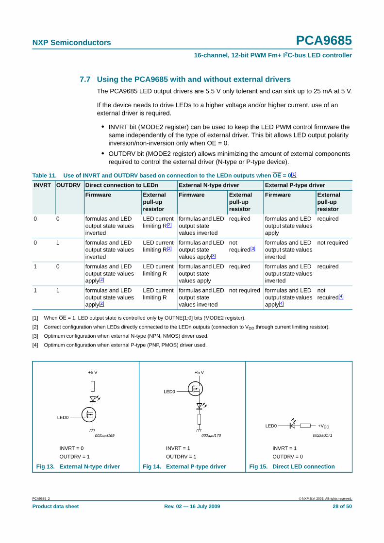
7.7 Using the PCA9685 with and without external driversThe PCA9685 LED output drivers are 5.5 V only tolerant and can sink up to 25 mA at 5 V.
If the device needs to drive LEDs to a higher voltage and/or higher current, use of anexternal driver is required.
• INVRT bit (MODE2 register) can be used to keep the LED PWM control firmware thesame independently of the type of external driver. This bit allows LED output polarityinversion/non-inversion only when OE = 0.
• OUTDRV bit (MODE2 register) allows minimizing the amount of external componentsrequired to control the external driver (N-type or P-type device).
[1] When OE = 1, LED output state is controlled only by OUTNE[1:0] bits (MODE2 register).
[2] Correct configuration when LEDs directly connected to the LEDn outputs (connection to VDD through current limiting resistor).
[3] Optimum configuration when external N-type (NPN, NMOS) driver used.
[4] Optimum configuration when external P-type (PNP, PMOS) driver used.
Table 11. Use of INVRT and OUTDRV based on connection to the LEDn outputs when OE = 0[1]
INVRT OUTDRV Direct connection to LEDn External N-type driver External P-type driver
Firmware Externalpull-upresistor
Firmware Externalpull-upresistor
Firmware Externalpull-upresistor
0 0 formulas and LEDoutput state valuesinverted
LED currentlimiting R[2]
formulas and LEDoutput statevalues inverted
required formulas and LEDoutput state valuesapply
required
0 1 formulas and LEDoutput state valuesinverted
LED currentlimiting R[2]
formulas and LEDoutput statevalues apply[3]
notrequired[3]
formulas and LEDoutput state valuesinverted
not required
1 0 formulas and LEDoutput state valuesapply[2]
LED currentlimiting R
formulas and LEDoutput statevalues apply
required formulas and LEDoutput state valuesinverted
required
1 1 formulas and LEDoutput state valuesapply[2]
LED currentlimiting R
formulas and LEDoutput statevalues inverted
not required formulas and LEDoutput state valuesapply[4]
notrequired[4]
INVRT = 0
OUTDRV = 1
INVRT = 1
OUTDRV = 1
INVRT = 1
OUTDRV = 0
Fig 13. External N-type driver Fig 14. External P-type driver Fig 15. Direct LED connection
LED0
+5 V
002aad169
LED0
+5 V
002aad170
LED0 +VDD
002aad171
PCA9685_2 © NXP B.V. 2009. All rights reserved.
Product data sheet Rev. 02 — 16 July 2009 28 of 50

NXP Semiconductors PCA968516-channel, 12-bit PWM Fm+ I 2C-bus LED controller
8. Characteristics of the I 2C-bus
The I2C-bus is for 2-way, 2-line communication between different ICs or modules. The twolines are a serial data line (SDA) and a serial clock line (SCL). Both lines must beconnected to a positive supply via a pull-up resistor when connected to the output stagesof a device. Data transfer may be initiated only when the bus is not busy.
8.1 Bit transferOne data bit is transferred during each clock pulse. The data on the SDA line must remainstable during the HIGH period of the clock pulse as changes in the data line at this timewill be interpreted as control signals (see Figure 16).
8.1.1 START and STOP conditions
Both data and clock lines remain HIGH when the bus is not busy. A HIGH-to-LOWtransition of the data line while the clock is HIGH is defined as the START condition (S). ALOW-to-HIGH transition of the data line while the clock is HIGH is defined as the STOPcondition (P) (see Figure 17).
8.2 System configurationA device generating a message is a ‘transmitter’; a device receiving is the ‘receiver’. Thedevice that controls the message is the ‘master’ and the devices which are controlled bythe master are the ‘slaves’ (see Figure 18).
Fig 16. Bit transfer
mba607
data linestable;
data valid
changeof dataallowed
SDA
SCL
Fig 17. Definition of START and STOP conditions
mba608
SDA
SCLP
STOP condition
S
START condition
PCA9685_2 © NXP B.V. 2009. All rights reserved.
Product data sheet Rev. 02 — 16 July 2009 29 of 50

NXP Semiconductors PCA968516-channel, 12-bit PWM Fm+ I 2C-bus LED controller
8.3 AcknowledgeThe number of data bytes transferred between the START and the STOP conditions fromtransmitter to receiver is not limited. Each byte of eight bits is followed by oneacknowledge bit. The acknowledge bit is a HIGH level put on the bus by the transmitter,whereas the master generates an extra acknowledge related clock pulse.
A slave receiver which is addressed must generate an acknowledge after the reception ofeach byte. Also a master must generate an acknowledge after the reception of each bytethat has been clocked out of the slave transmitter. The device that acknowledges has topull down the SDA line during the acknowledge clock pulse, so that the SDA line is stableLOW during the HIGH period of the acknowledge related clock pulse; set-up time and holdtime must be taken into account.
A master receiver must signal an end of data to the transmitter by not generating anacknowledge on the last byte that has been clocked out of the slave. In this event, thetransmitter must leave the data line HIGH to enable the master to generate a STOPcondition.
Fig 18. System configuration
002aaa966
MASTERTRANSMITTER/
RECEIVER
SLAVERECEIVER
SLAVETRANSMITTER/
RECEIVER
MASTERTRANSMITTER
MASTERTRANSMITTER/
RECEIVER
SDA
SCL
I2C-BUSMULTIPLEXER
SLAVE
Fig 19. Acknowledgement on the I 2C-bus
002aaa987
S
STARTcondition
9821
clock pulse foracknowledgement
not acknowledge
acknowledge
data outputby transmitter
data outputby receiver
SCL from master
PCA9685_2 © NXP B.V. 2009. All rights reserved.
Product data sheet Rev. 02 — 16 July 2009 30 of 50

NXP Semiconductors PCA968516-channel, 12-bit PWM Fm+ I 2C-bus LED controller
9. Bus transactions
(1) See Table 3 for register definition.
Fig 20. Write to a specific register
A5 A4 A3 A2 A1 A0 0 AS 1
slave address
START condition R/W acknowledgefrom slave
002aac829
data for register D[7:0](1)
D6 D5 D4 D3 D2 D1 D0D7
control register
A
acknowledgefrom slave
A
acknowledgefrom slave
P
STOPcondition
Fig 21. Write to all registers using the Auto-Increment feature; AI initially clear
A5 A4 A3 A2 A1 A0 0 AS 1
slave address
START condition R/W
002aad187
MODE1 register
0 0 0 0 0 0 00
control register = MODE1 register
A
acknowledgefrom slave
A
acknowledgefrom slave
P
STOPcondition
(cont.)
(cont.)
MODE2 register
A
acknowledgefrom slave
LED15_OFF_L register
A
acknowledgefrom slave
LED15_OFF_H register
A
acknowledgefrom slave
acknowledgefrom slave
1
AI bit set
PCA9685_2 © NXP B.V. 2009. All rights reserved.
Product data sheet Rev. 02 — 16 July 2009 31 of 50

NXP Semiconductors PCA968516-channel, 12-bit PWM Fm+ I 2C-bus LED controller
Fig 22. Read all registers using the Auto-Increment feature; AI initially clear
A5 A4 A3 A2 A1 A0 0 AS 1
slave address
START condition R/W
002aad188
MODE1 register
0 0 0 0 0 0 00
control register = MODE1 register
A
acknowledgefrom slave
A
acknowledgefrom slave
P
STOPcondition
(cont.)
(cont.)
data from MODE1
A
acknowledgefrom master
data from LED15_OFF_H register
A
not acknowledgefrom master
acknowledgefrom slave
1
AI bit set
Sr
ReSTARTcondition
A5 A4 A3 A2 A1 A0 11
slave address
R/W
A
acknowledgefrom slave
data from MODE2
A
acknowledgefrom master
Fig 23. Write to ALL_LED_ON and ALL_LED_OFF registers using the Auto-Increment feature; AI initially set
A5 A4 A3 A2 A1 A0 0 AS 1
slave address
START condition R/W
002aad189
ALL_LED_ON_L register
1 1 1 1 0 1 01
control register = ALL_LED_ON_L register
A
acknowledgefrom slave
A
acknowledgefrom slave
P
STOP condition
(cont.)
(cont.)
ALL_LED_ON_H register
A
acknowledgefrom slave
ALL_LED_OFF_L register
A
acknowledgefrom slave
ALL_LED_OFF_H register
A
acknowledgefrom slave
acknowledgefrom slave
Fig 24. Write to ALL_LED_OFF_H to turn OFF all PWMs
A5 A4 A3 A2 A1 A0 0 AS 1
slave address
START condition R/W
002aad190
1 1 1 1 1 0 11
control register = ALL_LED_OFF_H register
A
acknowledgefrom slave
P
STOPcondition
acknowledgefrom slave
0 0 1 X X X X0
ALL_LED_OFF_H register
A
acknowledgefrom slave
PCA9685_2 © NXP B.V. 2009. All rights reserved.
Product data sheet Rev. 02 — 16 July 2009 32 of 50

NXP Semiconductors PCA968516-channel, 12-bit PWM Fm+ I 2C-bus LED controller
(1) In this example, several PCA9685s are used and the same sequences (A) and (B) above are sent to each of them.
(2) Acknowledge from all the slave devices configured for the new LED All Call I2C-bus address in sequence (B).
Fig 25. LED All Call I 2C-bus address programming and LED All Call sequence example
A5 A4 A3 A2 A1 A0 0 AS 1
slave address
START condition R/W
acknowledgefrom slave
002aad192
0 0 0 0 0 0 00
control register
A
acknowledgefrom slave
MODE1register selection
0 1 0 0 1 1 10
data for MODE1 register
P
STOPcondition
A
acknowledgefrom slave
A5 A4 A3 A2 A1 A0 0 AS 1
slave address
START condition R/W
acknowledgefrom slave
0 0 0 0 1 0 10
control register
A
acknowledgefrom slave
ALLCALLADRregister selection
0 1 0 1 0 1 X1
new LEDALLCALL I2C-bus address
P
STOPcondition
A
acknowledgefrom slave
sequence (A)(1)
sequence (B)(1)
0 1 0 1 0 1 0 AS 1
LEDALLCALL I2C-bus address
START condition R/W
acknowledge(2) from all the devices configured for the new LEDALLCALL I2C-bus address
1 1 1 1 0 1 01
control register
A
acknowledge(2)
from slave
ALL_LED_ON_Lregister selection
0 0 0 0 0 0 00
data for control registerALL_LED_ON_L
P
STOPcondition
A
acknowledge(2)
from slave
sequence (C) (cont.)
(cont.) 0 0 0 0 0 0 0 A0 0 0 0 0 0 0 00 A
acknowledge(2)
from slave
data for ALL_LED_OFF_Lcontrol register
0 0 0 1 0 0 00 A
acknowledge(2)
from slave
ALL_LED_ON_Hcontrol register
acknowledge(2)
from slave
AI on enable ALL CALL
ALL_LED_OFF_H
PCA9685_2 © NXP B.V. 2009. All rights reserved.
Product data sheet Rev. 02 — 16 July 2009 33 of 50

NXP Semiconductors PCA968516-channel, 12-bit PWM Fm+ I 2C-bus LED controller
10. Application design-in information
I2C-bus address = 1010 101x.
All 16 of the LEDn outputs configurable as either open-drain or totem pole. Mixing of configuration is not possible.
Remark: Set INVRT = 0, OUTDRV = 1, OUTNE = 01 (MODE2 register bits)
(1) Resistor value should be chosen by referencing section 7 of UM10204, “I2C-bus specification and user manual”.
(2) OE requires pull-up resistor if control signal from the master is open-drain.
Fig 26. Typical application
PCA9685
LED0
LED1
SDA
SCL
OE
VDD = 2.5 V, 3.3 V or 5.0 V
I2C-BUS/SMBusMASTER
002aac827
SDA
SCL
(1)
OE
(1)
LED2
LED3
A0
A1
A2
VDD
A3
A4
A5
VSS
5 V
10 kΩ(2)
12 V
LED4
LED8
LED9
LED10
LED11
LED12
LED13
LED14
LED15
EXTCLK
5 V12 V
LED5
LED6
LED7
5 V12 V
5 V12 V
PCA9685_2 © NXP B.V. 2009. All rights reserved.
Product data sheet Rev. 02 — 16 July 2009 34 of 50

NXP Semiconductors PCA968516-channel, 12-bit PWM Fm+ I 2C-bus LED controller
Question 1: What kind of edge rate control is there on the outputs?
• The typical edge rates depend on the output configuration, supply voltage, and theapplied load. The outputs can be configured as either open-drain NMOS or totem poleoutputs. If the customer is using the part to directly drive LEDs, they should be using itin an open-drain NMOS, if they are concerned about the maximum ISS and groundbounce. The edge rate control was designed primarily to slow down the turn-on of theoutput device; it turns off rather quickly (~1.5 ns). In simulation, the typical turn-ontime for the open-drain NMOS was ~14 ns (VDD = 3.6 V; CL = 50 pF; RPU = 500 Ω).
Question 2: Is ground bounce possible?
• Ground bounce is a possibility, especially if all 16 outputs are changed at full current(25 mA each). There is a fair amount of decoupling capacitance on chip (~50 pF),which is intended to suppress some of the ground bounce. The customer will need todetermine if additional decoupling capacitance externally placed as close asphysically possible to the device is required.
Question 3: Can I really sink 400 mA through the single ground pin on the package andwill this cause any ground bounce problem due to the PWM of the LEDs?
• Yes, you can sink 400 mA through a single ground pin on the package . Although thepackage only has one ground pin, there are two ground pads on the die itselfconnected to this one pin. Although some ground bounce is likely, it will not disrupt theoperation of the part and would be reduced by the external decoupling capacitance.
Question 4: I can’t turn the LEDs on or off, but their registers are set properly. Why?
• Check the MODE1 register SLEEP (bit 4) setting. The bit needs to be 0 in order toenable the clocking. If both clock sources (internal osc and EXTCLK) are turned OFF(bit 4 = 1), the LEDs cannot be dimmed or blinked.
Question 5: I’m using LEDs with integrated Zener diodes and the IC is getting very hot.Why?
• The IC outputs can be set to either open-drain or push-pull and default to push-pulloutputs. In this application with the Zener diodes, they need to be set to open-drainsince in the push-pull architecture there is a low resistance path to GND through theZener and this is causing the IC to overheat.
PCA9685_2 © NXP B.V. 2009. All rights reserved.
Product data sheet Rev. 02 — 16 July 2009 35 of 50

NXP Semiconductors PCA968516-channel, 12-bit PWM Fm+ I 2C-bus LED controller
I2C-bus address = 1010 101x.
Remark: Set INVRT = 0, OUTDRV = 1, OUTNE = 01 (MODE2 register bits) for this configuration.
(1) Resistor value should be chosen by referencing Section 7 of UM10204, “I2C-bus specification anduser manual”.
(2) OE requires pull-up resistor if control signal from the master is open-drain.
Fig 27. LCD backlighting application
PCA9685
LED0
LED1
SDA
SCL
OE
VDD = 2.5 V, 3.3 V or 5.0 V
ASIC/MICRO
002aac828
SDA
SCL
(1)
OE
(1)
LED2
LED3
A0
A1
A2
VDD
A3
A4
A5
VSS
10 kΩ(2)
LED4
LED5
LED6
LED7
LED8
LED9
LED10
LED11
LED12
LED13
LED14
LED15
CONSTANTCURRENT
SWITCH MODEREGULATOR
FB
OUTVIN
Iconstant
LIGHTSENSOR
LED supply
Rsense
LEDstring
EXTCLK
PCA9685_2 © NXP B.V. 2009. All rights reserved.
Product data sheet Rev. 02 — 16 July 2009 36 of 50

NXP Semiconductors PCA968516-channel, 12-bit PWM Fm+ I 2C-bus LED controller
11. Limiting values
12. Static characteristics
Table 12. Limiting valuesIn accordance with the Absolute Maximum Rating System (IEC 60134).
Symbol Parameter Conditions Min Max Unit
VDD supply voltage −0.5 +6.0 V
VI/O voltage on an input/output pin VSS − 0.5 5.5 V
IO(LEDn) output current on pin LEDn - 25 mA
ISS ground supply current - 400 mA
Ptot total power dissipation - 400 mW
Tstg storage temperature −65 +150 °C
Tamb ambient temperature operating −40 +85 °C
Table 13. Static characteristicsVDD = 2.3 V to 5.5 V; VSS = 0 V; Tamb = −40 °C to +85 °C; unless otherwise specified.
Symbol Parameter Conditions Min Typ Max Unit
Supply
VDD supply voltage 2.3 - 5.5 V
IDD supply current operating mode; no load;fSCL = 1 MHz; VDD = 2.3 V to 5.5 V
- 6 10 mA
Istb standby current no load; fSCL = 0 Hz; VI = VDD or VSS;VDD = 2.3 V to 5.5 V
- 2.2 15.5 µA
VPOR power-on reset voltage no load; VI = VDD or VSS[1] - 1.70 2.0 V
Input SCL; input/output SDA
VIL LOW-level input voltage −0.5 - +0.3VDD V
VIH HIGH-level input voltage 0.7VDD - 5.5 V
IOL LOW-level output current VOL = 0.4 V; VDD = 2.3 V 20 28 - mA
VOL = 0.4 V; VDD = 5.0 V 30 40 - mA
IL leakage current VI = VDD or VSS −1 - +1 µA
Ci input capacitance VI = VSS - 6 10 pF
LED driver outputs
IOL LOW-level output current VOL = 0.5 V; VDD = 2.3 V to 4.5 V [2] 12 25 - mA
IOL(tot) total LOW-level output current VOL = 0.5 V; VDD = 4.5 V [2] - - 400 mA
IOH HIGH-level output current open-drain; VOH = VDD −10 - +10 µA
VOH HIGH-level output voltage IOH = −10 mA; VDD = 2.3 V 1.6 - - V
IOH = −10 mA; VDD = 3.0 V 2.3 - - V
IOH = −10 mA; VDD = 4.5 V 4.0 - - V
IOZ OFF-state output current 3-state; VOH = VDD or VSS −10 - +10 µA
Co output capacitance - 5 8 pF
PCA9685_2 © NXP B.V. 2009. All rights reserved.
Product data sheet Rev. 02 — 16 July 2009 37 of 50

NXP Semiconductors PCA968516-channel, 12-bit PWM Fm+ I 2C-bus LED controller
[1] VDD must be lowered to 0.2 V in order to reset part.
[2] Each bit must be limited to a maximum of 25 mA and the total package limited to 400 mA due to internal busing limits.
Address inputs; OE input; EXTCLK
VIL LOW-level input voltage −0.5 - +0.3VDD V
VIH HIGH-level input voltage 0.7VDD - 5.5 V
ILI input leakage current −1 - +1 µA
Ci input capacitance - 3 5 pF
Table 13. Static characteristics …continuedVDD = 2.3 V to 5.5 V; VSS = 0 V; Tamb = −40 °C to +85 °C; unless otherwise specified.
Symbol Parameter Conditions Min Typ Max Unit
Fig 28. IDD typical values with OSC on andfSCL = 1 MHz versus temperature
Fig 29. IOL typical drive (LEDn outputs) versustemperature
Fig 30. Standby supply current versus temperature
002aad877
Tamb (°C)−50 100500
4
6
2
8
10IDD
(mA)
0
VDD = 5.5 V
3.3 V
2.3 V
−50 100500
002aad878
20
40
60
IOL(mA)
0
Tamb (°C)
VDD = 4.5 V
3.0 V
2.3 V
002aad879
Tamb (°C)−50 100500
2
3
1
4
5Istb(µA)
0
VDD = 5.5 V
3.3 V
2.3 V
PCA9685_2 © NXP B.V. 2009. All rights reserved.
Product data sheet Rev. 02 — 16 July 2009 38 of 50

xxxx xxxxxxxxxxxxxxxxxxxxxxxxxxxxxx x xxxxxxxxxxxxxx xxxxxxxxxx xxx xxxxxx xxxxxxxxxxxxxxxxxxxxxxx xxxxxxxxxxxxxxxxxxxxxxxxxxx xxxxxx xx xxxxxxxxxxxxxxxxxxxxxxxxxxxxx xxxxxxxxxxxxxxxxxxxxxx xxxxxxxxxxx xxxxxxx xxxxxxxxxxxxxxxxxxxxxxxxxxxxxxxxxxx xxxxxxxxxxxxxx xxxxxx xx xxxxxxxxxxxxxxxxxxxxxxxxxxxxxxxx xxxxxxxxxxxxxxxxxxxxxxxx xxxxxxxxxxxxxxxxxxxxxxxxxxxxxxxxxxxxxxxxxxxxxxxxxxxxx xxxxxxxxxxx xxxxx x x
PC
A9685_2
Product data shee
NX
P S
emiconducto
13.D
ynamic cha
Table 14. Dynamic characteristics
Symbol Parameter Conditions Standard-modeI2C-bus
Fast-mode I 2C-bus Fast-mode PlusI2C-bus
Unit
Min Max Min Max Min Max
400 0 1000 kHz
50 DC 50 MHz
- 0.5 - µs
t fSCL SCL clock frequency [1] 0 100 0
fEXTCLK frequency on pin EXTCLK DC 50 DC
tBUF bus free time between a STOP 4.7 - 1.3
rsP
CA
968516-channel, 12-bit P
WM
Fm
+ I2C
-bus LED
controller
racteristics
- 0.26 - µs
- 0.26 - µs
- 0.26 - µs
- 0 - ns
0.9 0.05 0.45 µs
0.9 0.05 0.45 µs
- 50 - ns
- 0.5 - µs
- 0.26 - µs
300 - 120 ns
300 - 120 ns
50 - 50 ns
40 - 40 ns
60 - 60 ns
60 - 60 ns
© N
XP
B.V. 2009. A
ll rights reserved.
Rev. 02 —
16 July 200939 of 50
and START condition
tHD;STA hold time (repeated) STARTcondition
4.0 - 0.6
tSU;STA set-up time for a repeatedSTART condition
4.7 - 0.6
tSU;STO set-up time for STOP condition 4.0 - 0.6
tHD;DAT data hold time 0 - 0
tVD;ACK data valid acknowledge time [2] 0.3 3.45 0.1
tVD;DAT data valid time [3] 0.3 3.45 0.1
tSU;DAT data set-up time 250 - 100
tLOW LOW period of the SCL clock 4.7 - 1.3
tHIGH HIGH period of the SCL clock 4.0 - 0.6
tf fall time of both SDA and SCLsignals
[4][5] - 300 20 + 0.1Cb[6]
tr rise time of both SDA and SCLsignals
- 1000 20 + 0.1Cb[6]
tSP pulse width of spikes that mustbe suppressed by the input filter
[7] - 50 -
tPLZ LOW to OFF-state propagationdelay
OE to LEDn;OUTNE[1:0] = 10 or 11in MODE2 register
- 40 -
tPZL OFF-state to LOW propagationdelay
OE to LEDn;OUTNE[1:0] = 10 or 11in MODE2 register
- 60 -
tPHZ HIGH to OFF-state propagationdelay
OE to LEDn;OUTNE[1:0] = 10 or 11in MODE2 register
- 60 -

xxxxxxxxxxxxxxxxxxxxx xxxxxxxxxxxxxxxxxxxxxxxxxx xxxxxxx x x x xxxxxxxxxxxxxxxxxxxxxxxxxxxxxx xxxxxxxxxxxxxxxxxxx xx xxxxxxx xxxxxxxxxxxxxxxxxxxxxxxxxxx xxxxxxxxxxxxxxxxxxx xxxxxx xxxxxxxxxxxxxxxxxxxxxxxxxxxxxxxxxxx xxxxxxxxxxxx x xxxxxxxxxxxxxxxxxxxxxx xxxxxxxxxxxxxxxxxxxxxxxxxxxxxx xxxxx xxxxxxxxxxxxxxxxxxxxxxxxxxxxxxxxxxxxxxxxxxxxxxxxxx xxxxxxxxxxxxxxxxxxxxxxxxxxxxxxxxx xxxxxxxxxxxxxxxxxxxx xxx
PC
A9685_2
Product data shee
NX
P S
emiconductors
PC
A9685
16-channel, 12-bit PW
M F
m+ I
2C-bus LE
D controller
ld LOW for a minimum of 25 ms. Disable bus
to bridge the undefined region of SCL’s falling
ed at 250 ns. This allows series protectiond tf.
40 - 40 ns
40 - 40 ns
60 - 60 ns
Table 14. Dynamic characteristics …continued
Symbol Parameter Conditions Standard-modeI2C-bus
Fast-mode I 2C-bus Fast-mode PlusI2C-bus
Unit
Min Max Min Max Min Max
© N
XP
B.V. 2009. A
ll rights reserved.
tR
ev. 02 — 16 July 2009
40 of 50
[1] Minimum SCL clock frequency is limited by the bus time-out feature, which resets the serial bus interface if either SDA or SCL is hetime-out feature for DC operation.
[2] tVD;ACK = time for Acknowledgement signal from SCL LOW to SDA (out) LOW.
[3] tVD;DAT = minimum time for SDA data out to be valid following SCL LOW.
[4] A master device must internally provide a hold time of at least 300 ns for the SDA signal (refer to the VIL of the SCL signal) in orderedge.
[5] The maximum tf for the SDA and SCL bus lines is specified at 300 ns. The maximum fall time (tf) for the SDA output stage is specifiresistors to be connected between the SDA and the SCL pins and the SDA/SCL bus lines without exceeding the maximum specifie
[6] Cb = total capacitance of one bus line in pF.
[7] Input filters on the SDA and SCL inputs suppress noise spikes less than 50 ns.
tPZH OFF-state to HIGH propagationdelay
OE to LEDn;OUTNE[1:0] = 10 or 11in MODE2 register
- 40 -
tPLH LOW to HIGH propagation delay OE to LEDn;OUTNE[1:0] = 01in MODE2 register
- 40 -
tPHL HIGH to LOW propagation delay OE to LEDn;OUTNE[1:0] = 00in MODE2 register
- 60 -

NXP Semiconductors PCA968516-channel, 12-bit PWM Fm+ I 2C-bus LED controller
Fig 31. Definition of timing
tSPtBUF
tHD;STA
PP S
tLOW
tr
tHD;DAT
tf
tHIGH tSU;DAT
tSU;STA
Sr
tHD;STA
tSU;STO
SDA
SCL
002aaa986
Rise and fall times refer to VIL and VIH.
Fig 32. I2C-bus timing diagram
Fig 33. t PLZ, tPZL and t PHZ, tPZH times
SCL
SDA
tHD;STA tSU;DAT tHD;DAT
tftBUF
tSU;STA tLOW tHIGH
tVD;ACK
002aab285
tSU;STO
protocolSTART
condition(S)
bit 7MSB(A7)
bit 6(A6)
bit 1(D1)
bit 0(D0)
1 / fSCL
tr
tVD;DAT
acknowledge(A)
STOPcondition
(P)
002aad810
tPLZ
tPHZ
outputsdisabled
outputsenabled
outputsenabled
LEDn outputLOW-to-OFFOFF-to-LOW
LEDn outputHIGH-to-OFFOFF-to-HIGH
OE input
VI
VOL
VOH
VDD
VM
VM
VX
VY
VM
VSStPZL
tPZH
VM
VSS
PCA9685_2 © NXP B.V. 2009. All rights reserved.
Product data sheet Rev. 02 — 16 July 2009 41 of 50

NXP Semiconductors PCA968516-channel, 12-bit PWM Fm+ I 2C-bus LED controller
14. Test information
RL = Load resistor for LEDn.
CL = Load capacitance includes jig and probe capacitance.
RT = Termination resistance should be equal to the output impedance Zo of the pulse generators.
Fig 34. Test circuitry for switching times
RL = Load resistor for LEDn.
CL = Load capacitance includes jig and probe capacitance.
RT = Termination resistance should be equal to the output impedance Zo of the pulse generators.
Test data are given in Table 15.
Fig 35. Test circuitry for switching times for enable/disable
Table 15. Test data for enable/disable switching times
Test Load Switch
CL RL
tPD 50 pF 500 Ω open
tPLZ, tPZL 50 pF 500 Ω VDD × 2
tPHZ, tPZH 50 pF 500 Ω VSS
PULSEGENERATOR
VO
CL50 pF
RL500 Ω
002aab880
RT
VI
VDD
DUT
VDDopenVSS
PULSEGENERATOR
VO
CL50 pF
RL500 Ω
002aad811
RT
VI
VDD
DUT
RL500 Ω
VDD × 2openVSS
S1
PCA9685_2 © NXP B.V. 2009. All rights reserved.
Product data sheet Rev. 02 — 16 July 2009 42 of 50

NXP Semiconductors PCA968516-channel, 12-bit PWM Fm+ I 2C-bus LED controller
15. Package outline
Fig 36. Package outline SOT361-1 (TSSOP28)
UNIT A1 A2 A3 bp c D (1) E (2) (1)e HE L L p Q Zywv θ
REFERENCESOUTLINEVERSION
EUROPEANPROJECTION ISSUE DATE
IEC JEDEC JEITA
mm 0.150.05
0.950.80
0.300.19
0.20.1
9.89.6
4.54.3
0.656.66.2
0.40.3
0.80.5
80
o
o0.13 0.10.21
DIMENSIONS (mm are the original dimensions)
Notes
1. Plastic or metal protrusions of 0.15 mm maximum per side are not included.
2. Plastic interlead protrusions of 0.25 mm maximum per side are not included.
0.750.50
SOT361-1 MO-15399-12-2703-02-19
0.25
w Mbp
Z
e
1 14
28 15
pin 1 index
θ
AA1
A2
Lp
Q
detail X
L
(A )3
HE
E
c
v M A
XAD
y
0 2.5 5 mm
scale
TSSOP28: plastic thin shrink small outline package; 28 leads; body width 4.4 mm SOT361-1
Amax.
1.1
PCA9685_2 © NXP B.V. 2009. All rights reserved.
Product data sheet Rev. 02 — 16 July 2009 43 of 50

NXP Semiconductors PCA968516-channel, 12-bit PWM Fm+ I 2C-bus LED controller
Fig 37. Package outline SOT788-1 (HVQFN28)
0.651
A1 Ehb cUNIT ye
REFERENCESOUTLINEVERSION
EUROPEANPROJECTION ISSUE DATE
IEC JEDEC JEITA
mm 6.15.9
6.15.9
Dh
4.253.95
y1
4.253.95
e1
3.9
e2
3.90.350.25
0.050.00
0.2 0.05 0.1
DIMENSIONS (mm are the original dimensions)
SOT788-1 MO-220- - - - - -
0.750.50
L
0.1
v
0.05
w
0 2.5 5 mm
scale
SOT788-1HVQFN28: plastic thermal enhanced very thin quad flat package; no leads;28 terminals; body 6 x 6 x 0.85 mm
A(1)
max.
A A1c
detail X
yy1 Ce
L
Eh
Dh
e
e1
b8 14
28 22
21
157
1
X
D
E
C
B A
e2
02-10-22
terminal 1index area
terminal 1index area
ACC
Bv M
w M
Note
1. Plastic or metal protrusions of 0.075 mm maximum per side are not included.
D(1) E(1)
PCA9685_2 © NXP B.V. 2009. All rights reserved.
Product data sheet Rev. 02 — 16 July 2009 44 of 50

NXP Semiconductors PCA968516-channel, 12-bit PWM Fm+ I 2C-bus LED controller
16. Handling information
All input and output pins are protected against ElectroStatic Discharge (ESD) undernormal handling. When handling ensure that the appropriate precautions are taken asdescribed in JESD625-A or equivalent standards.
17. Soldering of SMD packages
This text provides a very brief insight into a complex technology. A more in-depth accountof soldering ICs can be found in Application Note AN10365 “Surface mount reflowsoldering description”.
17.1 Introduction to solderingSoldering is one of the most common methods through which packages are attached toPrinted Circuit Boards (PCBs), to form electrical circuits. The soldered joint provides boththe mechanical and the electrical connection. There is no single soldering method that isideal for all IC packages. Wave soldering is often preferred when through-hole andSurface Mount Devices (SMDs) are mixed on one printed wiring board; however, it is notsuitable for fine pitch SMDs. Reflow soldering is ideal for the small pitches and highdensities that come with increased miniaturization.
17.2 Wave and reflow solderingWave soldering is a joining technology in which the joints are made by solder coming froma standing wave of liquid solder. The wave soldering process is suitable for the following:
• Through-hole components
• Leaded or leadless SMDs, which are glued to the surface of the printed circuit board
Not all SMDs can be wave soldered. Packages with solder balls, and some leadlesspackages which have solder lands underneath the body, cannot be wave soldered. Also,leaded SMDs with leads having a pitch smaller than ~0.6 mm cannot be wave soldered,due to an increased probability of bridging.
The reflow soldering process involves applying solder paste to a board, followed bycomponent placement and exposure to a temperature profile. Leaded packages,packages with solder balls, and leadless packages are all reflow solderable.
Key characteristics in both wave and reflow soldering are:
• Board specifications, including the board finish, solder masks and vias
• Package footprints, including solder thieves and orientation
• The moisture sensitivity level of the packages
• Package placement
• Inspection and repair
• Lead-free soldering versus SnPb soldering
17.3 Wave solderingKey characteristics in wave soldering are:
PCA9685_2 © NXP B.V. 2009. All rights reserved.
Product data sheet Rev. 02 — 16 July 2009 45 of 50

NXP Semiconductors PCA968516-channel, 12-bit PWM Fm+ I 2C-bus LED controller
• Process issues, such as application of adhesive and flux, clinching of leads, boardtransport, the solder wave parameters, and the time during which components areexposed to the wave
• Solder bath specifications, including temperature and impurities
17.4 Reflow solderingKey characteristics in reflow soldering are:
• Lead-free versus SnPb soldering; note that a lead-free reflow process usually leads tohigher minimum peak temperatures (see Figure 38) than a SnPb process, thusreducing the process window
• Solder paste printing issues including smearing, release, and adjusting the processwindow for a mix of large and small components on one board
• Reflow temperature profile; this profile includes preheat, reflow (in which the board isheated to the peak temperature) and cooling down. It is imperative that the peaktemperature is high enough for the solder to make reliable solder joints (a solder pastecharacteristic). In addition, the peak temperature must be low enough that thepackages and/or boards are not damaged. The peak temperature of the packagedepends on package thickness and volume and is classified in accordance withTable 16 and 17
Moisture sensitivity precautions, as indicated on the packing, must be respected at alltimes.
Studies have shown that small packages reach higher temperatures during reflowsoldering, see Figure 38.
Table 16. SnPb eutectic process (from J-STD-020C)
Package thickness (mm) Package reflow temperature ( °C)
Volume (mm 3)
< 350 ≥ 350
< 2.5 235 220
≥ 2.5 220 220
Table 17. Lead-free process (from J-STD-020C)
Package thickness (mm) Package reflow temperature ( °C)
Volume (mm 3)
< 350 350 to 2000 > 2000
< 1.6 260 260 260
1.6 to 2.5 260 250 245
> 2.5 250 245 245
PCA9685_2 © NXP B.V. 2009. All rights reserved.
Product data sheet Rev. 02 — 16 July 2009 46 of 50

NXP Semiconductors PCA968516-channel, 12-bit PWM Fm+ I 2C-bus LED controller
For further information on temperature profiles, refer to Application Note AN10365“Surface mount reflow soldering description”.
18. Abbreviations
MSL: Moisture Sensitivity Level
Fig 38. Temperature profiles for large and small components
001aac844
temperature
time
minimum peak temperature= minimum soldering temperature
maximum peak temperature= MSL limit, damage level
peak temperature
Table 18. Abbreviations
Acronym Description
CDM Charged-Device Model
DUT Device Under Test
EMI ElectroMagnetic Interference
ESD ElectroStatic Discharge
HBM Human Body Model
I2C-bus Inter-Integrated Circuit bus
LCD Liquid Crystal Display
LED Light Emitting Diode
LSB Least Significant Bit
MM Machine Model
MSB Most Significant Bit
NMOS Negative-channel Metal-Oxide Semiconductor
PCB Printed-Circuit Board
PMOS Positive-channel Metal-Oxide Semiconductor
POR Power-On Reset
PWM Pulse Width Modulation; Pulse Width Modulator
RGB Red/Green/Blue
RGBA Red/Green/Blue/Amber
SMBus System Management Bus
PCA9685_2 © NXP B.V. 2009. All rights reserved.
Product data sheet Rev. 02 — 16 July 2009 47 of 50

NXP Semiconductors PCA968516-channel, 12-bit PWM Fm+ I 2C-bus LED controller
19. Revision history
Table 19. Revision history
Document ID Release date Data sheet status Change notice Supersedes
PCA9685_2 20090716 Product data sheet - PCA9685_1
Modifications: • Table 1 “Ordering information”:
– added type number PCA9685PW/Q900
– added Table note [1]
• Figure 2 “Pin configuration for TSSOP28”: added type number PCA9685PW/Q900
PCA9685_1 20080724 Product data sheet - -
PCA9685_2 © NXP B.V. 2009. All rights reserved.
Product data sheet Rev. 02 — 16 July 2009 48 of 50

NXP Semiconductors PCA968516-channel, 12-bit PWM Fm+ I 2C-bus LED controller
20. Legal information
20.1 Data sheet status
[1] Please consult the most recently issued document before initiating or completing a design.
[2] The term ‘short data sheet’ is explained in section “Definitions”.
[3] The product status of device(s) described in this document may have changed since this document was published and may differ in case of multiple devices. The latest product statusinformation is available on the Internet at URL http://www.nxp.com.
20.2 Definitions
Draft — The document is a draft version only. The content is still underinternal review and subject to formal approval, which may result inmodifications or additions. NXP Semiconductors does not give anyrepresentations or warranties as to the accuracy or completeness ofinformation included herein and shall have no liability for the consequences ofuse of such information.
Short data sheet — A short data sheet is an extract from a full data sheetwith the same product type number(s) and title. A short data sheet is intendedfor quick reference only and should not be relied upon to contain detailed andfull information. For detailed and full information see the relevant full datasheet, which is available on request via the local NXP Semiconductors salesoffice. In case of any inconsistency or conflict with the short data sheet, thefull data sheet shall prevail.
20.3 Disclaimers
General — Information in this document is believed to be accurate andreliable. However, NXP Semiconductors does not give any representations orwarranties, expressed or implied, as to the accuracy or completeness of suchinformation and shall have no liability for the consequences of use of suchinformation.
Right to make changes — NXP Semiconductors reserves the right to makechanges to information published in this document, including withoutlimitation specifications and product descriptions, at any time and withoutnotice. This document supersedes and replaces all information supplied priorto the publication hereof.
Suitability for use — NXP Semiconductors products are not designed,authorized or warranted to be suitable for use in medical, military, aircraft,space or life support equipment, nor in applications where failure ormalfunction of an NXP Semiconductors product can reasonably be expectedto result in personal injury, death or severe property or environmental
damage. NXP Semiconductors accepts no liability for inclusion and/or use ofNXP Semiconductors products in such equipment or applications andtherefore such inclusion and/or use is at the customer’s own risk.
Applications — Applications that are described herein for any of theseproducts are for illustrative purposes only. NXP Semiconductors makes norepresentation or warranty that such applications will be suitable for thespecified use without further testing or modification.
Limiting values — Stress above one or more limiting values (as defined inthe Absolute Maximum Ratings System of IEC 60134) may cause permanentdamage to the device. Limiting values are stress ratings only and operation ofthe device at these or any other conditions above those given in theCharacteristics sections of this document is not implied. Exposure to limitingvalues for extended periods may affect device reliability.
Terms and conditions of sale — NXP Semiconductors products are soldsubject to the general terms and conditions of commercial sale, as publishedat http://www.nxp.com/profile/terms, including those pertaining to warranty,intellectual property rights infringement and limitation of liability, unlessexplicitly otherwise agreed to in writing by NXP Semiconductors. In case ofany inconsistency or conflict between information in this document and suchterms and conditions, the latter will prevail.
No offer to sell or license — Nothing in this document may be interpretedor construed as an offer to sell products that is open for acceptance or thegrant, conveyance or implication of any license under any copyrights, patentsor other industrial or intellectual property rights.
Export control — This document as well as the item(s) described hereinmay be subject to export control regulations. Export might require a priorauthorization from national authorities.
20.4 TrademarksNotice: All referenced brands, product names, service names and trademarksare the property of their respective owners.
I2C-bus — logo is a trademark of NXP B.V.
21. Contact information
For more information, please visit: http://www .nxp.com
For sales office addresses, please send an email to: salesad [email protected]
Document status [1] [2] Product status [3] Definition
Objective [short] data sheet Development This document contains data from the objective specification for product development.
Preliminary [short] data sheet Qualification This document contains data from the preliminary specification.
Product [short] data sheet Production This document contains the product specification.
PCA9685_2 © NXP B.V. 2009. All rights reserved.
Product data sheet Rev. 02 — 16 July 2009 49 of 50

NXP Semiconductors PCA968516-channel, 12-bit PWM Fm+ I 2C-bus LED controller
22. Contents
1 General description . . . . . . . . . . . . . . . . . . . . . . 12 Features . . . . . . . . . . . . . . . . . . . . . . . . . . . . . . . 23 Applications . . . . . . . . . . . . . . . . . . . . . . . . . . . . 34 Ordering information . . . . . . . . . . . . . . . . . . . . . 35 Block diagram . . . . . . . . . . . . . . . . . . . . . . . . . . 46 Pinning information . . . . . . . . . . . . . . . . . . . . . . 56.1 Pinning . . . . . . . . . . . . . . . . . . . . . . . . . . . . . . . 56.2 Pin description . . . . . . . . . . . . . . . . . . . . . . . . . 57 Functional description . . . . . . . . . . . . . . . . . . . 67.1 Device addresses . . . . . . . . . . . . . . . . . . . . . . . 67.1.1 Regular I2C-bus slave address . . . . . . . . . . . . . 67.1.2 LED All Call I2C-bus address . . . . . . . . . . . . . . 77.1.3 LED Sub Call I2C-bus addresses . . . . . . . . . . . 77.1.4 Software Reset I2C-bus address . . . . . . . . . . . 87.2 Control register . . . . . . . . . . . . . . . . . . . . . . . . . 87.3 Register definitions . . . . . . . . . . . . . . . . . . . . . . 97.3.1 Mode register 1, MODE1 . . . . . . . . . . . . . . . . 137.3.1.1 Restart mode . . . . . . . . . . . . . . . . . . . . . . . . . 147.3.2 Mode register 2, MODE2 . . . . . . . . . . . . . . . . 157.3.3 LED output and PWM control . . . . . . . . . . . . . 157.3.4 ALL_LED_ON and ALL_LED_OFF control. . . 247.3.5 PWM frequency PRE_SCALE . . . . . . . . . . . . 247.3.6 SUBADR1 to SUBADR3, I2C-bus
subaddress 1 to 3 . . . . . . . . . . . . . . . . . . . . . . 257.3.7 ALLCALLADR, LED All Call I2C-bus
address . . . . . . . . . . . . . . . . . . . . . . . . . . . . . . 257.4 Active LOW output enable input . . . . . . . . . . . 267.5 Power-on reset . . . . . . . . . . . . . . . . . . . . . . . . 267.6 Software reset. . . . . . . . . . . . . . . . . . . . . . . . . 277.7 Using the PCA9685 with and without
external drivers . . . . . . . . . . . . . . . . . . . . . . . . 288 Characteristics of the I 2C-bus. . . . . . . . . . . . . 298.1 Bit transfer . . . . . . . . . . . . . . . . . . . . . . . . . . . 298.1.1 START and STOP conditions . . . . . . . . . . . . . 298.2 System configuration . . . . . . . . . . . . . . . . . . . 298.3 Acknowledge . . . . . . . . . . . . . . . . . . . . . . . . . 309 Bus transactions . . . . . . . . . . . . . . . . . . . . . . . 3110 Application design-in information . . . . . . . . . 3411 Limiting values. . . . . . . . . . . . . . . . . . . . . . . . . 3712 Static characteristics. . . . . . . . . . . . . . . . . . . . 3713 Dynamic characteristics . . . . . . . . . . . . . . . . . 3914 Test information . . . . . . . . . . . . . . . . . . . . . . . . 4215 Package outline . . . . . . . . . . . . . . . . . . . . . . . . 4316 Handling information. . . . . . . . . . . . . . . . . . . . 4517 Soldering of SMD packages . . . . . . . . . . . . . . 45
17.1 Introduction to soldering. . . . . . . . . . . . . . . . . 4517.2 Wave and reflow soldering . . . . . . . . . . . . . . . 4517.3 Wave soldering. . . . . . . . . . . . . . . . . . . . . . . . 4517.4 Reflow soldering. . . . . . . . . . . . . . . . . . . . . . . 4618 Abbreviations . . . . . . . . . . . . . . . . . . . . . . . . . 4719 Revision history . . . . . . . . . . . . . . . . . . . . . . . 4820 Legal information . . . . . . . . . . . . . . . . . . . . . . 4920.1 Data sheet status . . . . . . . . . . . . . . . . . . . . . . 4920.2 Definitions . . . . . . . . . . . . . . . . . . . . . . . . . . . 4920.3 Disclaimers. . . . . . . . . . . . . . . . . . . . . . . . . . . 4920.4 Trademarks . . . . . . . . . . . . . . . . . . . . . . . . . . 4921 Contact information . . . . . . . . . . . . . . . . . . . . 4922 Contents. . . . . . . . . . . . . . . . . . . . . . . . . . . . . . 50
© NXP B.V. 2009. All rights reserved.For more information, please visit: http://www.nxp.comFor sales office addresses, please send an email to: [email protected]
Date of release: 16 July 2009
Document identifier: PCA9685_2
Please be aware that important notices concerning this document and the product(s)described herein, have been included in section ‘Legal information’.