PC/104-Plus Specification
27
PC/104-Plus Specification Version 2.2 January 2007 Please Note This specification is subject to change without notice. While every effort has been made to ensure the accuracy of the material contained within this document, the PC/104 Embedded Consortium shall under no circumstances be liable for incidental or consequential damages or related expenses resulting from the use of this specification. If errors are found, please notify the PC/104 Embedded Consortium. PC/104, PC/104-Plus, and PCI-104 are trademarks of the PC/104 Embedded Consortium. All other marks are the property of their respective companies. Copyright 1992-2007, PC/104 Embedded Consortium
Transcript of PC/104-Plus Specification

PC/104-Plus Specification
Version 2.2
January 2007
Please Note This specification is subject to change without notice. While every effort has been made to ensure the accuracy of the material contained within this document, the PC/104 Embedded Consortium shall under no circumstances be liable for incidental or consequential damages or related expenses resulting from the use of this specification. If errors are found, please notify the PC/104 Embedded Consortium. PC/104, PC/104-Plus, and PCI-104 are trademarks of the PC/104 Embedded Consortium. All other marks are the property of their respective companies.
Copyright 1992-2007, PC/104 Embedded Consortium

PC/104-Plus Specification Version — Page i
REVISION HISTORY Draft 0.7, November 20, 1996 - Preliminary Draft a. Formatted to meet the requirements of the PC/104 Consortium. b. Modify the component restrictions across and to each side of the PC/104 connectors (three sides, .400“ from each
edge, 4.35" top clearance, .100" bottom clearance). Draft 0.8, December 16, 1996 - Cleanup for Release a. Correct general typos. b. Correct word reference error. c. Add QuickSwitch part number and clarify Mux requirements. d. Change PCI ONLY to PCI-Only and add note. e. Correct Figure 4 and Figure 5 errors. f. Correct typo in Table 3. Draft 0.9, January 10, 1997 - Cleanup for Release a. Cleanup minor grammatical errors. Version 1.0, February 1997 - Initial Release a. Grammatical changes and cleanup per review recommendations. b. Change Footnote 1 on Page 4 to show future support for the M66EN (66MHz Enable) signal. c. Add signals PRSNT[1:2]# and CLKRUN# to Figure 2 to encompass all unused PCI signals. d. Moved the Mechanical section after the Electrical section. e. Clarified the KEY pin usage for universal modules and defined them as ground connections. f. Clarified pin 1 for the PC/104-Plus connectors on Figure 6. g. Added an example manufacturer and part No. for the PCI connector (Figure 7) and Shroud (Figure 8). h. Modified , Table 1, and some text under Section 3.2 to add routing recommendations for the PCI interrupt lines
INTA - INTD. Version 1.1, June 1997 - Minor Editorial Corrections a. Correct errors in the Table of Figures and Table of Tables. b. Correct dimensions on the PCI connector (Figure 5). c. Correct part number and dimensions on the shroud (Figure 6). d. Correct general typos and update reference information. Version 1.2, April 2001 a. Added PCI Connector Specifications and PCI-104 name for “PCI Only”. b. Added PC/104 8-Bit and 16-Bit Connector Specification. c. Removed specific company references. d. Corrected PCISIG and consortium addresses and phone numbers.

PC/104-Plus Specification Version — Page ii
Version 2.0, November, 2003 a. Chapter 1. Introduction and contact information updated b. Chapter 2. PCI Signal Definition
1. All PCI signal names have been updated to reflect the PCI Specification Version 2.2 2. Signals SBO* and SDONE have been removed to reflect PCI Version 2.2 3. “(Not Supported)” has been placed under the Present signal in Figure 2 4. PCI signal descriptions in section 2.1 have been updated to reflect the PCI Specification Version 2.2 5. Section 2.2 has been updated with additional figures and descriptions to help clarify the purpose for signal
selection on the expansion modules. Figure 2 and Table 1 reflect the addition of a 4th GNT# and REQ# pair to allow for a 4th bus mastering expansion module on a PC/104-Plus stack. The “ID Address” column has been removed from table 1 since this is dependent on the PCI Host module.
c. Chapter 3. Electrical Specification 1. References to PCI specification Version 2.1 have been change to PCI Specification Version 2.2 2. Section 3.2.4 “Key Locations has been eliminated. Description for the identification of the PCI signaling type
has been moved to the “Mechanical Specification” chapter 3. Note 1 of Table 2 has been changed to reflect that the Host board does not need to supply 3.3V to the PCI bus
if it is using 3.3V PCI signaling. As with 5V PCI signaling Host cards, it is up to the user to supply 3.3V to the stack.
4. New section on PCI Signaling Voltage (VI/O) Requirements was added. This section discusses 3.3V, 5V, and Universal Add-In Cards
d. Chapter 4. Levels of Conformance 1. PCI-104 section was removed since it will be covered in its own Specification Manual
e. Chapter 5. Mechanical Specifications 1. Section on clock trace lengths was added 2. A section has been added “Board Identifier” which describes how to label a board to indicate its PCI signaling
voltage level capabilities. This replaces the keying of the PCI connector. f. Appendix A. Mechanical Dimensions
1. Figure 4 has been redone in AutoCAD showing both English and Metric units. The shroud keep out region was also added. So was an area for connector overhang at the lower right hand side of the ISA bus.
2. Figure 5: Note 1 “DIN 41612 Part 5 “ has been removed since this does not apply to the PCI connector 3. Contact finish female interface changed from 20 micoinches minimum to 15 microinches in Figures 9 & 11 4. Mechanical performance withdrawal force changed from 1 ounce minimum average to 1 ounce per pin
minimum in Figures 9 & 11 g. Appendix B. Bus Signal Assignments
1. Pin B30 (Reserved) replaced with REQ3# 2. Pin C30 (Reserved) replaced with GNT3# 3. Pin C9 (SBO*) replaced with Reserved to reflect the PCI Local Bus Specification Revision 2.2 4. Pin D10 (SDONE) replaced with Reserved to reflect the PCI Local Bus Specification Revision 2.2 5. Note 2 at the bottom of Table 3 has been removed
h. Specification has been reformatted and updated 1. Chapter 2 “PCI Signal Definition” is now Chapter 3. 2. Chapter 3 “Electrical Specification” is now Chapter 4. 3. Chapter 4 “Levels of Conformance” is now Chapter 5. 4. Chapter 5 “Mechanical Specifications” is now Chapter 6. 5. Chapter 6 “Typical Stack” is now Chapter 2
Version 2.1, November, 2006 a. Chapter 1. Introduction
1. PC/104 Embedded Consortium contact information has been updated. b. Chapter 3. PCI Signal Definition
1. Figure 4: “INTE#” corrected to “INTA#”. Version 2.2, January, 2007 a. Figure 4. Added “complementary” to description of Rotary Switch.
PC/104-Plus Specification Version — Page iii
TABLE OF CONTENTS
1. INTRODUCTION.............................................................................................................................1 1.1 SUMMARY OF KEY DIFFERENCES FROM PC/104 SPECIFICATION:...............................................1 1.2 SUMMARY OF KEY DIFFERENCES (120-PIN PCI AND PCI LOCAL BUS SPECIFICATION) .............1 1.3 REFERENCES.................................................................................................................................2
2. A POSSIBLE MODULE STACK CONFIGURATION ................................................................3
3. PCI SIGNAL DEFINITION ............................................................................................................4 3.1 PCI BUS SIGNAL DESCRIPTION ....................................................................................................5
3.1.1 Address and Data.................................................................................................................5 3.1.2 Interface Control Pins..........................................................................................................5 3.1.3 Error Reporting....................................................................................................................5 3.1.4 Arbitration (Bus Masters Only)...........................................................................................5 3.1.5 System .................................................................................................................................6 3.1.6 Interrupts .............................................................................................................................6
3.2 SIGNAL GROUPING .......................................................................................................................7 4. ELECTRICAL SPECIFICATION................................................................................................10
4.1 ISA BUSES..................................................................................................................................10 4.2 PCI BUS......................................................................................................................................10
4.2.1 Signal Definitions..............................................................................................................10 4.2.2 Signal Assignments ...........................................................................................................10 4.2.3 Power and Ground Pins .....................................................................................................10 4.2.4 AC/DC Signal Specifications ............................................................................................10
4.3 MODULE POWER REQUIREMENTS..............................................................................................11 4.4 PCI SIGNALING VOLTAGE (VI/O) REQUIREMENTS....................................................................11
4.4.1 PCI Host Module...............................................................................................................11 4.4.2 Add-In Modules ................................................................................................................11
5. LEVELS OF CONFORMANCE ...................................................................................................12 5.1 PC/104-PLUS "COMPLIANT"......................................................................................................12 5.2 PC/104-PLUS "BUS-COMPATIBLE" ............................................................................................12
6. MECHANICAL SPECIFICATION..............................................................................................13 6.1 ISA CONNECTOR ........................................................................................................................13 6.2 PCI CONNECTOR ........................................................................................................................13
6.2.1 Clock Trace Lengths..........................................................................................................13 6.2.2 Module Dimensions...........................................................................................................13 6.2.3 Connector and Shroud .......................................................................................................13 6.2.4 Board Identifier .................................................................................................................13
APPENDICES
A. MECHANICAL DIMENSIONS ...................................................................................................... A-1
B. BUS SIGNAL ASSIGNMENTS ........................................................................................................B-1

PC/104-Plus Specification Version — Page iv
TABLE OF FIGURES
FIGURE 1: A POSSIBLE MODULE STACK CONFIGURATION................................................................ 3
FIGURE 2: PCI PIN LIST.................................................................................................................... 4
FIGURE 3: INTERRUPT ROUTING FOR A DESKTOP PC......................................................................... 7
FIGURE 4: SIGNAL SELECT ON AN EXPANSION BOARD ..................................................................... 8
FIGURE 5: INT# SELECT................................................................................................................... 9
FIGURE 6: PC/104-PLUS MODULE DIMENSIONS...........................................................................A-2
FIGURE 7: PCI CONNECTOR .........................................................................................................A-3
FIGURE 8: PCI CONNECTOR SHROUD ...........................................................................................A-3
FIGURE 9: PCI CONNECTOR SPECIFICATIONS ...............................................................................A-4
FIGURE 10: 8-BIT AND 16-BIT ISA CONNECTOR (REFERENCE ONLY)..........................................A-5
FIGURE 11: 8-BIT AND 16-BIT ISA CONNECTOR SPECIFICATION (REFERENCE ONLY) .................A-6
TABLE OF TABLES
TABLE 1: ROTARY SWITCH SETTINGS .............................................................................................. 9
TABLE 2: MODULE POWER REQUIREMENTS ................................................................................... 11
TABLE 3: PCI BUS SIGNAL ASSIGNMENTS ................................................................................... B-2
TABLE 4: ISA BUS (REFERENCE ONLY) ....................................................................................... B-3

PC/104-Plus Specification Version 2.2 — Page 1
PC/104-Plus SPECIFICATION Version 2.2
1. INTRODUCTION
The ISA architecture bus has long been a popular choice for embedded applications. With the publication of the PC/104 standard in 1992, this bus architecture was available on a small, rugged form factor which has since become an industry standard. As technological requirements advanced, a need began to arise for a higher performance bus throughput. This is especially true when it comes to graphics devices as well as other high-speed I/O devices such as networks. The PC/104 Consortium met this challenge by incorporating a PCI bus on the PC/104 form factor, which became to be known as PC/104-Plus. This architecture provides a link to versatile legacy hardware while meeting the high-speed requirements for present and future hardware. This document supplies the mechanical and electrical specifications for the “PC/104-Plus” and incorporates all of the PC/104 features, with the added advantage of the high speed PCI bus. The physical size, mounting configuration and electrical interconnect portion of the PC/104 specification shall remain unchanged.
1.1 Summary of Key Differences From PC/104 Specification:
A third connector opposite the ISA connectors supports the PCI bus. The component height on the topside has been reduced from 0.435" to 0.345" and the bottom
has been increased from 0.100" to 0.190" to increase the flexibility of the module. Control logic added to handle the requirements for the high-speed bus.
1.2 Summary of Key Differences (120-pin PCI and PCI Local Bus Specification)
The PCI bus connector is a 4x30 (120-pin) 2mm pitch stack-through connector as opposed to the 124-pin edge connector on standard 32-bit PCI Local Bus.
The 120-pin PCI does not support 64-bit Extensions, JTAG, PRSNT, or CLKRUN signals.

PC/104-Plus Specification Version 2.2 — Page 2
1.3 References
This document covers the addition of the PCI functions. The following documents should be used as reference for a detailed understanding of the overall system requirements: PC/104 Specification -- Version 2.5 PCI Local Bus Specification Revision 2.2
Contact the PCI Special Interest Group office for the latest revision of the PCI specification:
PCI Special Interest Group 5440 SW Westgate Dr., #217
Portland, OR 97221 Phone: 503.291.2569 Fax: 503.297.1090
Email: [email protected] Website: http://www.pcisig.com
If errors are found in this document, please send a written copy of the suggested corrections to:
PC/104 Embedded Consortium 505 Beach Street, Suite 130
San Francisco, CA 94133 USA Tel: 415.674.4504 / Fax: 415.674.4539
E-mail: [email protected] / Website: http://www.pc104.org

PC/104-Plus Specification Version 2.2 — Page 3
2. A POSSIBLE MODULE STACK CONFIGURATION
Figure 1 shows a typical module stack with two PC/104-Plus modules, one PC/104 16-bit module, and one PC/104 8-bit module. The maximum configuration for the PCI bus of PC/104-Plus modules is four plus the Host Board. If standard PC/104 modules are used in the stack, they must be the top module(s) because they will normally not include the PCI bus.
Figure 1: A Possible Module Stack Configuration
0.6 in. (15mm) Spacers (4 plcs.)
0.6 in. (15mm) Spacers (4 plcs.)
0.6 in. (15mm) Spacers (4 plcs.)
Stack-through 8-bit module
Stack-through 16-bit module
Stack-through PC/104-Plus
Non-stack-throughPC/104-Plus
0.6 in (15mm)
0.435 in (11mm)

PC/104-Plus Specification Version 2.2 — Page 4
3. PCI SIGNAL DEFINITION
Figure 2 shows the pins in functional groups, with the required pins on the left and the optional pins on the right side. The shaded pins on the right are unsupported features, but are included to show the entire PCI bus as defined in the PCI Local Bus Specification Revision 2.2. This version of the PCI bus is intended as a 32-bit bus running at 33MHz and therefore, 64-bit extension and 66MHz1 are not supported at this time. Also not supported are the boundary scan features (JTAG), Present (PRSNT[1:2]#), and Clock running (CLKRUN#). The direction indication on the pins assumes a combination master/target device.
Figure 2: PCI Pin List
1 The PCI bus has been simulated at 33MHz. For the purpose of this specification, 66MHz is not supported. To support future enhancements, the M66EN signal should be grounded on any module that cannot support 66MHz and left open for modules that can support a 66MHz clock.
Arbitration (master only)
TRST#
ACK64# REQ64# PAR64
AD[63:32]
IRDY#
DEVSEL#
LOCK#
RST# CLK
GNT# REQ#
SERR# PERR#
IDSEL
STOP#
TRDY# FRAME#
PAR
C/BE[3:0]#
AD[31:00]
INTD# INTC# INTB# INTA# Address
& Data
Interface Control
Interface Control
Error Reporting
System
Interrupts
PCI COMPLIANT
DEVICE
TMS TCK TDO TDI
JTAG (Not Supported)
C/BE[7:4]# 64-Bit Extension (Not Supported)
M66EN1 66MHz Enable
CLKRUN# Clock Running (Not Supported)
PRSNT[1:2]# Present (Not Supported)
Required Pins Optional Pins

PC/104-Plus Specification Version 2.2 — Page 5
3.1 PCI Bus Signal Description
3.1.1 Address and Data
AD[31:00] Address and Data are multiplexed on the same PCI pins. A bus transaction consists of an address phase followed by one or more data phases.
C/BE[3:0]# Bus Command/Byte Enables are multiplexed. During the address phase of a transaction, they define the bus command. During the data phase, they are used as byte enables.
PAR Parity is even parity across AD[31:00] and C/BE[3:0]#. Parity generation is required by all PCI signals.
3.1.2 Interface Control Pins
FRAME# Cycle Frame is driven by the current master to indicate the beginning of an access and will remain active until the final data cycle.
TRDY# Target Ready indicates the selected device’s ability to complete the current data phase of the transaction. Both IRDY# and TRDY# must be asserted to terminate a data cycle.
IRDY# Initiator Ready indicates the bus master's ability to complete the current data phase of the transaction.
STOP# Stop indicates the current selected device is requesting the master to stop the current transaction.
DEVSEL# Device Select, when actively driven, indicates the driving device has decoded its address as the target of the current access.
IDSEL Initialization Device Select is used as a chip-select during configuration read and write transactions.
LOCK# Lock indicates an atomic operation to a bridge that may require multiple transactions to complete.
3.1.3 Error Reporting
PERR# Parity Error is for reporting data parity errors. SERR# System Error is for reporting address parity errors.
3.1.4 Arbitration (Bus Masters Only)
REQ# Request indicates to the arbitrator that this device desires use of the bus. GNT# Grant indicates to the requesting device that access has been granted.

PC/104-Plus Specification Version 2.2 — Page 6
3.1.5 System
CLK Clock provides timing for all transactions on the PCI bus and is an input to every PCI device.
RST# Reset is used to bring PCI-specific registers, sequencers, and signals to a consistent state.
M66EN 66 MHz Enable indicates to a device whether the bus segment is operating at 33 MHz or 66 MHz. The PCI bus has been simulated at 33MHz. For the purpose of this specification, 66MHz is not supported. To support future enhancements, the M66EN signal should be grounded on any module that cannot support 66MHz and left open for modules that can support a 66MHz clock.
3.1.6 Interrupts
INTA# Interrupt A is used to request Interrupts. INTB# Interrupt B is used to request Interrupts. INTC# Interrupt C is used to request Interrupts. INTD# Interrupt D is used to request Interrupts.

PC/104-Plus Specification Version 2.2 — Page 7
3.2 Signal Grouping
The PC/104-Plus architecture was developed to take advantage of the versatility and simplicity of the PC market for embedded applications. Like the desktop PC, PC/104-Plus has the ability to add auxiliary boards to expand the capabilities of the CPU. But instead of using slot cards, PC/104-Plus adds additional modules using stack-through connectors. This has two advantages: it reduces the system size and it makes the system more rugged so that it can better withstand shocks and vibrations. To realize a stack-through architecture, a means of selecting the appropriate signals for each expansion card must be established that will easily allow for the installation and configuration of add-in PC/104-Plus and PCI-104 modules. The signals in question include the CLKx, IDSELx, REQx#, GNTx#, and INTx# lines. Normal desktop computers overcome this problem by routing only the necessary signals to each of the slot connectors. For example, on a desktop PC, only CLK1, IDSEL1, REQ1#, and GNT1# are routed to PCI slot 1. Likewise, CLK2, IDSEL2, REQ2#, and GNT2# are routed to slot 2. The interrupts on a desktop PC are handled in a different manner. All four interrupts from the interrupt controller are routed to each PCI slot connector. By convention INTA# on an expansion card is used for single-function devices and the remaining interrupts are used in the case of multi-functional devices. This could place a large burden on INTA# since all of the expansion cards would use this interrupt. To alleviate the burden, PC manufacturers stagger the interrupts on the motherboard to each of the PCI connectors. This is shown in Figure 3.
Figure 3: Interrupt routing for a desktop PC
PCI Host
INTA#
INTD# INTC# INTB#
INTX#
INTW# INTZ# INTY#
INTW#
INTZ# INTY# INTX#
MotherboardPCI
Slotboard 1 PCI
Slotboard 2
PCI Connector 1
PCI Connector 2
PCI Connector 3
INTA#
INTD# INTC# INTB#
INTY#
INTX#INTW#INTZ#
INTA#
INTD#INTC#INTB#
INTA#
INTD#INTC#INTB#
INTQA
INTD#INTC#INTB#

PC/104-Plus Specification Version 2.2 — Page 8
Since PC/104-Plus is a stack-through architecture, there is only one connector to which all of the expansion boards must connect. A means of selecting the appropriate signals must be established that will easily allow for the installation and configuration of add-in PC/104-Plus and PCI-104 modules. Figure 4 shows such a method that can be applied to the expansion boards.
Figure 4: Signal Select on an Expansion Board
The multiplexer chips on the expansion board serve as the equivalent of having multiple PCI slot connectors on the motherboard of a desktop PC. To select the appropriate REQ#, GNT#, CLK, and INT signals for the expansion module, the rotary switch must be adjusted for the position on the stack.
IDSEL0 IDSEL1 IDSEL2 IDSEL3
CLK0 CLK1 CLK2 CLK3
CLK
IDSEL
A0 A1
EN#
DUAL 4 TO 1 MUX
0123
0123
REQ#
GNT#
REQ0#REQ1#REQ2#REQ3#
GNT0#GNT1#GNT2#GNT3#
A0 A1
vcc
6
1
2
4
Complementary Rotary Switch
0 1 2 4 3 5 7
C
EN#
DUAL 4 TO 1 MUX 0
123
0123
INT0#
INT1#
INTA#INTB#INTC#INTD#
INTB#INTC#INTD#INTA#
A0 A1
EN#
DUAL 4 TO 1 MUX 0
123
0123
This Mux is Only Required for Bus Masters
1 or 2 Muxes are recommended for INTA Routing.
See Table 1 for routing of INT2# and INT3#.

PC/104-Plus Specification Version 2.2 — Page 9
For expansion modules requiring more than one interrupt, the staggering of the INTx# lines is accomplished on the expansion module prior to the multiplexers. Figure 5 shows the interrupt routing on a PCI Host Module and on an expansion module with two functions. The Add-on Module portion of Figure 5 shows how the right-hand multiplexer of Figure 4 fits onto an add-on module. If a board has a single function then only half of the multiplexer is required.
Figure 5: INT# Select
The multiplexer chips are Dual 4:1 Mux/Demux chips. They provide a 5Ω switch that connects the input and output together. These switches provide a bi-directional path with no signal propagation delay other than the RC delay of the on resistance of the switch and the load capacitance. This is typically 250ps at 50pF load. Use one Mux for 1 to 2 interrupts or two Muxes for 3 to 4 interrupts. While other methods of configuring the modules are possible and permissible, the rotary switch is clean and provides for the least possible error in configuration. Table 1 shows the appropriate switch setting and signals used for each module in the stack.
Table 1: Rotary Switch Settings Switch Position Module Slot REQ# GNT# CLK INT0# INT1# INT2# INT3#
0 or 4 1 REQ0# GNT0# CLK0 INTA# INTB# INTC# INTD# 1 or 5 2 REQ1# GNT1# CLK1 INTB# INTC# INTD# INTA# 2 or 6 3 REQ2# GNT2# CLK2 INTC# INTD# INTA# INTB# 3 or 7 4 REQ3# GNT3# CLK3 INTD# INTA# INTB# INTC#
PCI Host
INTW# INTX# INTY# INTZ#
PCI Conn.
INTA#INTB#INTC#INTD# Dual
4 to 1MUX
PCI Conn.
INTA# INTB# INTC# INTD# PCI
Device
INT0# INT1#
PCI Host Module Add-on Module
INTB# INTC# INTD# INTA#
INTA#INTB#INTC#INTD#

PC/104-Plus Specification Version 2.2 — Page 10
4. ELECTRICAL SPECIFICATION
4.1 ISA Buses
The electrical specifications for the 8-bit and 16-bit ISA buses for bus drive current, bus termination, pullup/pulldown resistors, etc. are unchanged and are defined in the PC/104 Specification. The signal assignments for the J1/P1 and J2/P2 connector are given in Appendix B, Table 4: ISA Bus (Reference Only).
4.2 PCI Bus
The PCI Bus mechanical interface is a stackable 4x30 header. This interface carries all of the required PCI signals per PCI Local Bus Specification Revision 2.2.
4.2.1 Signal Definitions
For full details on the electrical requirements for the PCI bus, reference the PCI Local Bus Specification Revision 2.2.
4.2.2 Signal Assignments
Signals are assigned in the same relative order as in the PCI Local Bus Specification Revision 2.2, but transformed to the corresponding header connector pins. Because of the stack-through nature of the bus, slot-specific signals are duplicated for each plug-in module. The system has been designed to accommodate 4 modules, which are PC/104-Plus, PCI-104, or a combination of the two, so multiple sets of the signals have been duplicated to accommodate one signal for each module. These four signal groups include: IDSEL[3:0], CLK[3:0], REQ#[3:0], GNT#[3:0]. Signal assignments for the J3/P3 connector are given in Appendix B, Table 3: PCI Bus Signal Assignments.
4.2.3 Power and Ground Pins
The total number of power and ground signals remains the same, but the +3.3 V pins have been reduced by two and the ground pins have been increased by two. The change was the result of signal grouping on the bus and has no effect on performance or integrity.
4.2.4 AC/DC Signal Specifications
All bus timing and signal levels are identical to the PCI Local Bus Specification Revision 2.2.

PC/104-Plus Specification Version 2.2 — Page 11
4.3 Module Power Requirements
Table 2 specifies the voltage and maximum power requirements for each PC/104-Plus module. Care should be used in designing PC/104-Plus modules to guarantee the least possible power consumption. A worst case module as specified could use almost 39 Watts of power, which would be unacceptable in most systems.
Table 2: Module Power Requirements
Supply Min. Voltage Max. Voltage Max. Current Max. Power +3.3V1 3.00 3.60 3A 10.8W
+5V 4.75 5.25 2A 10.5W +12V 11.4 12.6 1A 12.6W -5V -5.25 -4.75 0.2A 1.05W
-12V -12.6 -11.4 0.3A 3.78W Note 1: Host Boards implementing “5 volt PCI signaling” are not required to supply 3.3 volts to the modules,
but must provide a bus and decoupling. Host Boards implementing “3.3 volt PCI signaling” are not required to supply 5 volts to the modules, but must provide a bus and decoupling.
4.4 PCI Signaling Voltage (VI/O) Requirements
4.4.1 PCI Host Module
The PCI Host board will always determine the PCI signaling level on the bus by setting all VI/O pins to either 3.3V or 5V. If VI/O is set to 3.3V, then the system will use 3.3V I/O signaling and, likewise, if VI/O is set to 5V, then the system will use 5V I/O signaling. Some PCI host modules may only allow one of the options, while others may provide a jumper to allow the user to select the signaling level. Once the signaling level is selected, the remaining boards in the system must use that signaling level.
4.4.2 Add-In Modules
Add-in cards can be 3.3V, 5V, or universal.
3.3V Add-In Modules 3.3V add-in modules operate in environments where VI/O has been set to 3.3V by the host module. Using 5V add-in modules on a 3.3V stack will result in the 3.3V modules being damaged. 5V Add-In Modules 5V add-in modules operate in environments where VI/O has been set to 5V by the host module. Using 3.3V add-in modules on a 5V stack will result in the 3.3V modules being damaged. Universal Add-In Modules Universal add-in board can be used on either 3V or 5V I/O signaling buses. Universal boards either use the VI/O signal to determine its signaling level or are 3V signaling boards that have 5V-tolerant I/O. Many PCI interface chips have a "VI/O" pin that is the power for the I/O buffers that can be directly connected to VI/O. Universal boards will work on either 3V or 5V I/O signaling buses.
PC/104-Plus Specification Version 2.2 — Page 12
5. LEVELS OF CONFORMANCE
This section provides terminology intended to assist manufacturers and users of PC/104-Plus bus-compatible products in defining and specifying conformance with the PC/104-Plus Specification. 5.1 PC/104-Plus "Compliant"
This refers to "PC/104-Plus form-factor" devices that conform to all non-optional aspects of the PC/104-Plus Specification, including both mechanical and electrical specifications. 5.2 PC/104-Plus "Bus-compatible"
This refers to devices which are not "PC/104-Plus form-factor" (i.e., do not comply with the module dimensions of the PC/104-Plus Specification), but provide male or female PC/104-Plus bus connectors that meets both the mechanical and electrical specifications provided for the PC/104-Plus bus connectors.
PC/104-Plus Specification Version 2.2 — Page 13
6. MECHANICAL SPECIFICATION
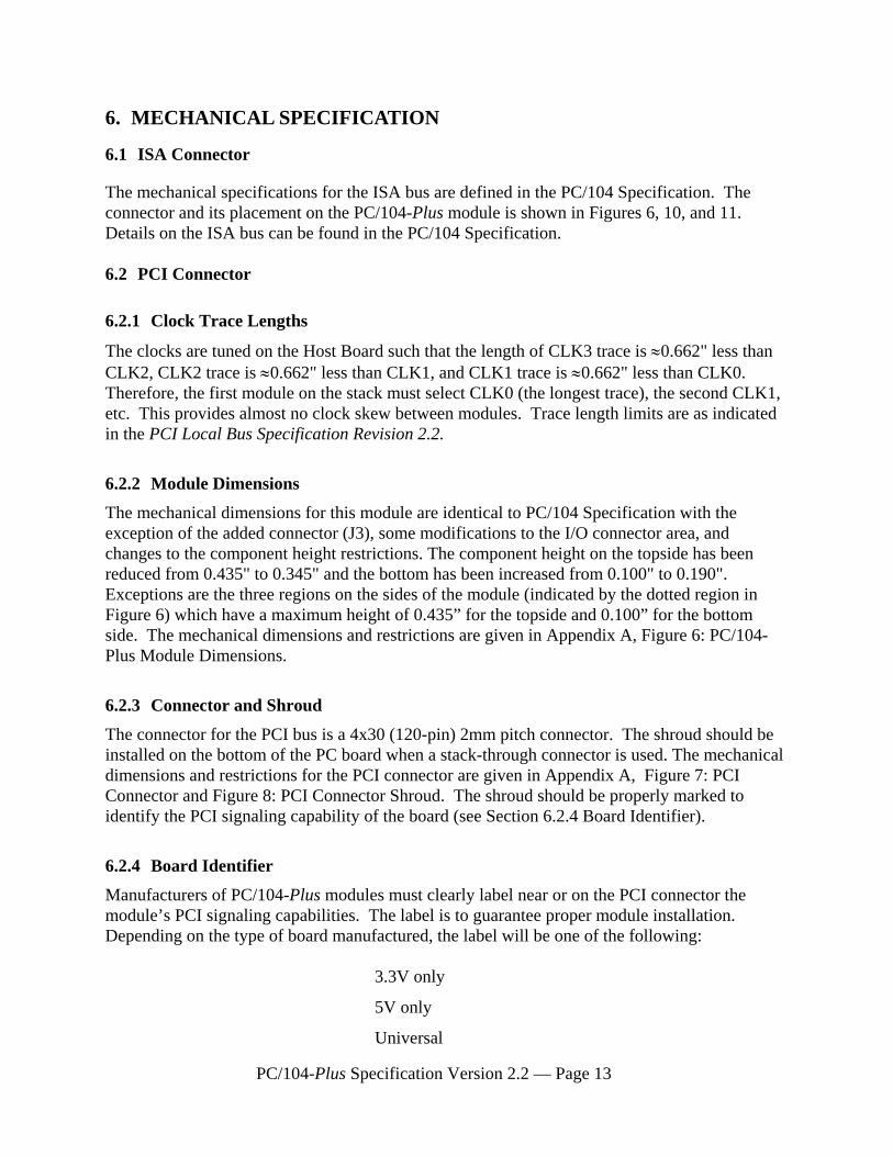
6.1 ISA Connector
The mechanical specifications for the ISA bus are defined in the PC/104 Specification. The connector and its placement on the PC/104-Plus module is shown in Figures 6, 10, and 11. Details on the ISA bus can be found in the PC/104 Specification. 6.2 PCI Connector
6.2.1 Clock Trace Lengths
The clocks are tuned on the Host Board such that the length of CLK3 trace is ≈0.662" less than CLK2, CLK2 trace is ≈0.662" less than CLK1, and CLK1 trace is ≈0.662" less than CLK0. Therefore, the first module on the stack must select CLK0 (the longest trace), the second CLK1, etc. This provides almost no clock skew between modules. Trace length limits are as indicated in the PCI Local Bus Specification Revision 2.2.
6.2.2 Module Dimensions
The mechanical dimensions for this module are identical to PC/104 Specification with the exception of the added connector (J3), some modifications to the I/O connector area, and changes to the component height restrictions. The component height on the topside has been reduced from 0.435" to 0.345" and the bottom has been increased from 0.100" to 0.190". Exceptions are the three regions on the sides of the module (indicated by the dotted region in Figure 6) which have a maximum height of 0.435” for the topside and 0.100” for the bottom side. The mechanical dimensions and restrictions are given in Appendix A, Figure 6: PC/104-Plus Module Dimensions.
6.2.3 Connector and Shroud
The connector for the PCI bus is a 4x30 (120-pin) 2mm pitch connector. The shroud should be installed on the bottom of the PC board when a stack-through connector is used. The mechanical dimensions and restrictions for the PCI connector are given in Appendix A, Figure 7: PCI Connector and Figure 8: PCI Connector Shroud. The shroud should be properly marked to identify the PCI signaling capability of the board (see Section 6.2.4 Board Identifier).
6.2.4 Board Identifier
Manufacturers of PC/104-Plus modules must clearly label near or on the PCI connector the module’s PCI signaling capabilities. The label is to guarantee proper module installation. Depending on the type of board manufactured, the label will be one of the following:
3.3V only
5V only
Universal
PC/104-Plus Specification Version 2.2 — Page A-1
APPENDIX A
MECHANICAL DIMENSIONS

PC/104-Plus Specification Version 2.2 — Page A-2
Figure 6: PC/104-Plus Module Dimensions
Dimensions are in inches / (millimeters)

PC/104-Plus Specification Version 2.2 — Page A-3
Figure 7: PCI Connector
Figure 8: PCI Connector Shroud

PC/104-Plus Specification Version 2.2 — Page A-4
Figure 9: PCI Connector Specifications
MATERIALS Housing: High Temp Thermoplastic, UL Rated 94-V0 Contact: Phosphor Bronze Solder: Tin-Lead (63-37), If Applicable Solder Clip: Aluminum Alloy, If Applicable CONTACT FINISH Female Interface: 15 Microinches Minimum Hard Gold Male Interface: Gold Flash Minimum Solder Tail: 100 Microinches Minimum Solder Underplate: 50 Microinches Minimum Nickel MECHANICAL PERFORMANCE Insertion Force: 2.5 Ounce Per Pin Maximum Withdrawal Force: 1 Ounce Per Pin Minimum Normal Force: 50 Grams Minimum (Per Beam) Durability: 50 Cycles Minimum Operating Temp: -55° C To +85° C Minimum ELECTRICAL PERFORMANCE Contact Resistance: <30 Milliohms Maximum Current Capacity: 1 Amp Continuous Per Pin Dielectric Strength: 500 Vac Insulation Resistance: 5,000 Megohms Minimum

PC/104-Plus Specification Version 2.2 — Page A-5
Figure 10: 8-Bit and 16-Bit ISA Connector (Reference Only)

PC/104-Plus Specification Version 2.2 — Page A-6
Figure 11: 8-Bit and 16-Bit ISA Connector Specification (Reference Only)
MATERIALS Housing: High Temp Thermoplastic, UL Rated 94-V0 Contact: Phosphor Bronze Solder: Tin-Lead (63-37), If Applicable Solder Clip: Aluminum Alloy, If Applicable CONTACT FINISH Female Interface: 15 Microinches Minimum Hard Gold Male Interface: Gold Flash Minimum Solder Tail: 100 Microinches Minimum Solder Underplate: 50 Microinches Minimum Nickel MECHANICAL PERFORMANCE Insertion Force: 3.5 Ounce Per Pin Maximum Withdrawal Force: 1 Ounce Per Pin Minimum Normal Force: 50 Grams Minimum (Per Beam) Durability: 50 Cycles Minimum Operating Temp: -55° C To +85° C Minimum ELECTRICAL PERFORMANCE Contact Resistance: <30 Milliohms Maximum Current Capacity: 1 Amp Continuous Per Pin Dielectric Strength: 1000 Vac Insulation Resistance: 5,000 Megohms Minimum

PC/104-Plus Specification Version 2.2 — Page B-1
APPENDIX B
BUS SIGNAL ASSIGNMENTS

PC/104-Plus Specification Version 2.2 — Page B-2
Table 3: PCI Bus Signal Assignments
J3/P3
Pin A B C D 1 GND Reserved +5 AD00 2 VI/O AD02 AD01 +5V 3 AD05 GND AD04 AD03 4 C/BE0# AD07 GND AD06 5 GND AD09 AD08 GND 6 AD11 VI/O AD10 M66EN 7 AD14 AD13 GND AD12 8 +3.3V C/BE1# AD15 +3.3V 9 SERR# GND Reserved PAR
10 GND PERR# +3.3V Reserved 11 STOP# +3.3V LOCK# GND 12 +3.3V TRDY# GND DEVSEL# 13 FRAME# GND IRDY# +3.3V 14 GND AD16 +3.3V C/BE2# 15 AD18 +3.3V AD17 GND 16 AD21 AD20 GND AD19 17 +3.3V AD23 AD22 +3.3V 18 IDSEL0 GND IDSEL1 IDSEL2 19 AD24 C/BE3# VI/O IDSEL3 20 GND AD26 AD25 GND 21 AD29 +5V AD28 AD27 22 +5V AD30 GND AD31 23 REQ0# GND REQ1# VI/O 24 GND REQ2# +5V GNT0# 25 GNT1# VI/O GNT2# GND 26 +5V CLK0 GND CLK1 27 CLK2 +5V CLK3 GND 28 GND INTD# +5V RST# 29 +12V INTA# INTB# INTC# 30 -12V REQ3# GNT3# GND
Note: 1. The shaded area denotes power or ground signals.

PC/104-Plus Specification Version 2.2 — Page B-3
Table 4: ISA Bus (Reference Only)
J1/P1 Pin Row A Row B 1 IOCHK* GND 2 SD7 RESET 3 SD6 +5V 4 SD5 IRQ9 5 SD4 -5V 6 SD3 DRQ2
J2/P2 7 SD2 -12V Pin Row D Row C 8 SD1 SRDY* 0 GND GND 9 SD0 +12V 1 MEMCS16* SBHE* 10 IOCHRDY KEY 2 IOCS16* LA23 11 AEN SMEMW* 3 IRQ10 LA22 12 SA19 SMEMR* 4 IRQ11 LA21 13 SA18 IOW* 5 IRQ12 LA20 14 SA17 IOR* 6 IRQ15 LA19 15 SA16 DACK3* 7 IRQ14 LA18 16 SA15 DRQ3 8 DACK0* LA17 17 SA14 DACK1* 9 DRQ0 MEMR* 18 SA13 DRQ1
10 DACK5* MEMW* 19 SA12 REFRESH* 11 DRQ5 SD8 20 SA11 BCLK 12 DACK6* SD9 21 SA10 IRQ7 13 DRQ6 SD10 22 SA9 IRQ6 14 DACK7* SD11 23 SA8 IRQ5 15 DRQ7 SD12 24 SA7 IRQ4 16 +5V SD13 25 SA6 IRQ3 17 MASTER16* SD14 26 SA5 DACK2* 18 GND SD15 27 SA4 TC 19 GND KEY 28 SA3 BALE
29 SA2 +5V 30 SA1 OSC 31 SA0 GND 32 GND GND