Market Research Report : PC Peripherals Market in India 2012
Upload
truongkienCategory
view
232download
5
Computer Architecture 2010 – PC Structure and Peripherals1
Computer ArchitectureComputer Architecture
PC Structure and PeripheralsPC Structure and Peripherals
Slides byDr. Lihu Rappoport
Computer Architecture 2010 – PC Structure and Peripherals2
MemoryMemory
Computer Architecture 2010 – PC Structure and Peripherals3
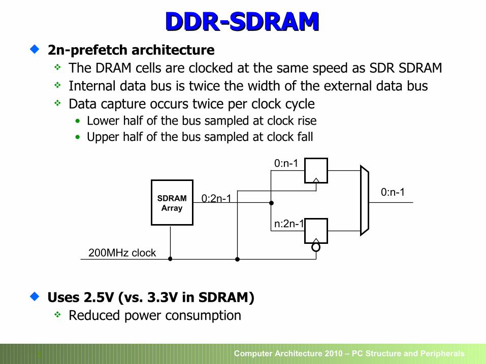
DDR-SDRAMDDR-SDRAM◆ 2n-prefetch architecture
The DRAM cells are clocked at the same speed as SDR SDRAM Internal data bus is twice the width of the external data bus Data capture occurs twice per clock cycle
• Lower half of the bus sampled at clock rise• Upper half of the bus sampled at clock fall
◆ Uses 2.5V (vs. 3.3V in SDRAM) Reduced power consumption
0:n-1
n:2n-1
0:n-1
200MHz clock
0:2n-1SDRAMArray
Computer Architecture 2010 – PC Structure and Peripherals4
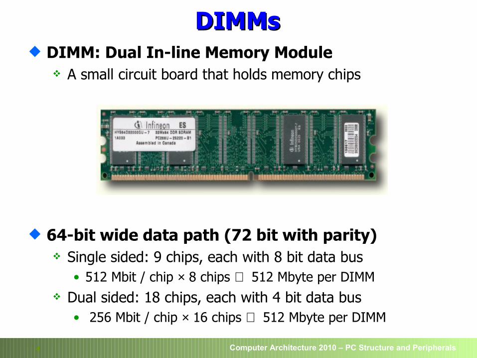
DIMMsDIMMs◆ DIMM: Dual In-line Memory Module
A small circuit board that holds memory chips
◆ 64-bit wide data path (72 bit with parity) Single sided: 9 chips, each with 8 bit data bus
• 512 Mbit / chip × 8 chips ⇒ 512 Mbyte per DIMM Dual sided: 18 chips, each with 4 bit data bus
• 256 Mbit / chip × 16 chips ⇒ 512 Mbyte per DIMM
Computer Architecture 2010 – PC Structure and Peripherals5
DDR2DDR2
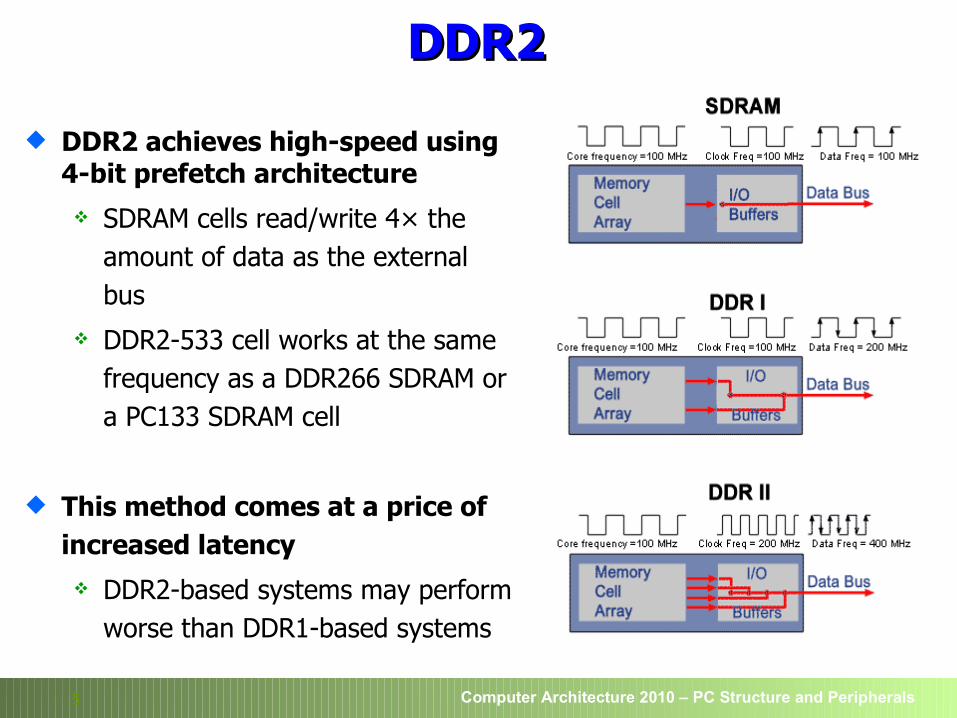
◆ DDR2 achieves high-speed using 4-bit prefetch architecture
SDRAM cells read/write 4× the amount of data as the external bus
DDR2-533 cell works at the same frequency as a DDR266 SDRAM or a PC133 SDRAM cell
◆ This method comes at a price of increased latency
DDR2-based systems may perform worse than DDR1-based systems
Computer Architecture 2010 – PC Structure and Peripherals6
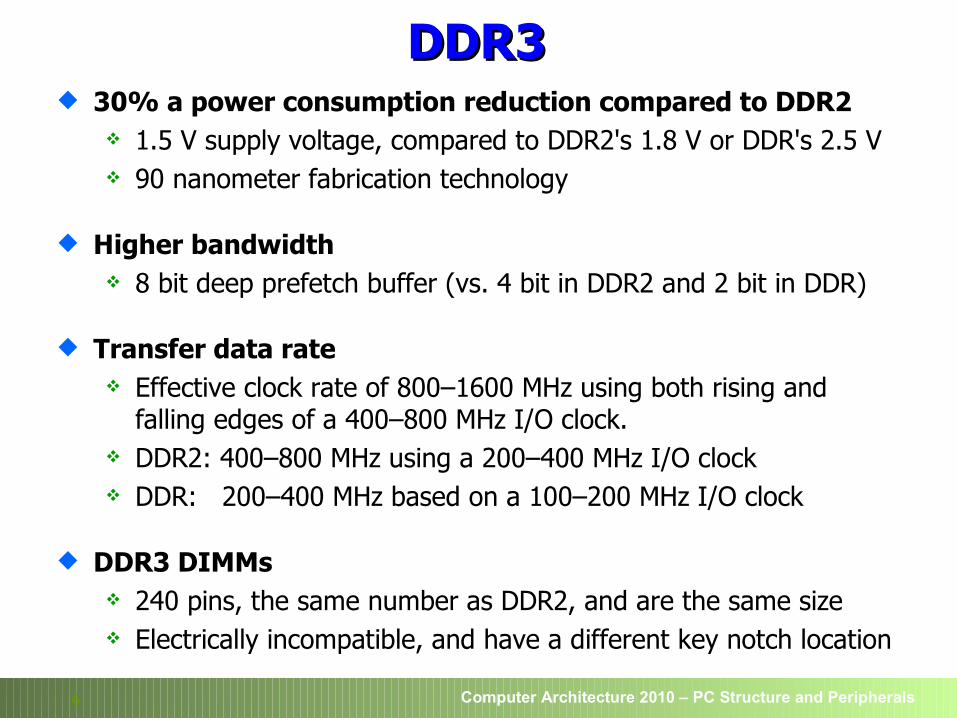
DDR3DDR3◆ 30% a power consumption reduction compared to DDR2
1.5 V supply voltage, compared to DDR2's 1.8 V or DDR's 2.5 V 90 nanometer fabrication technology
◆ Higher bandwidth 8 bit deep prefetch buffer (vs. 4 bit in DDR2 and 2 bit in DDR)
◆ Transfer data rate Effective clock rate of 800–1600 MHz using both rising and
falling edges of a 400–800 MHz I/O clock. DDR2: 400–800 MHz using a 200–400 MHz I/O clock DDR: 200–400 MHz based on a 100–200 MHz I/O clock
◆ DDR3 DIMMs 240 pins, the same number as DDR2, and are the same size Electrically incompatible, and have a different key notch location
Computer Architecture 2010 – PC Structure and Peripherals7
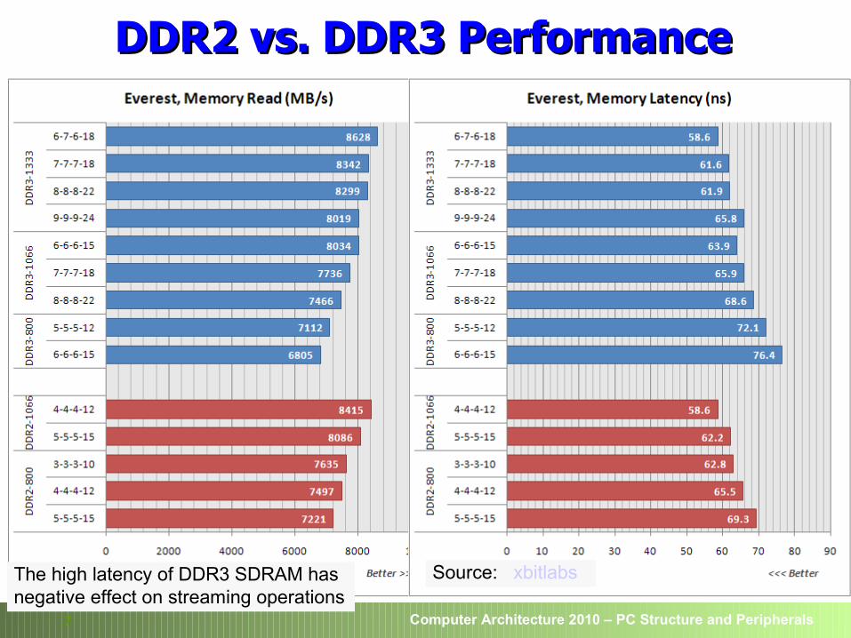
DDR2 vs. DDR3 PerformanceDDR2 vs. DDR3 Performance
The high latency of DDR3 SDRAM has negative effect on streaming operations
Source: xbitlabs
Computer Architecture 2010 – PC Structure and Peripherals8
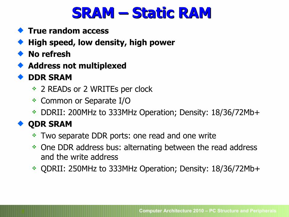
SRAM – Static RAM SRAM – Static RAM ◆ True random access◆ High speed, low density, high power◆ No refresh◆ Address not multiplexed◆ DDR SRAM
2 READs or 2 WRITEs per clock Common or Separate I/O DDRII: 200MHz to 333MHz Operation; Density: 18/36/72Mb+
◆ QDR SRAM Two separate DDR ports: one read and one write One DDR address bus: alternating between the read address
and the write address QDRII: 250MHz to 333MHz Operation; Density: 18/36/72Mb+
Computer Architecture 2010 – PC Structure and Peripherals9
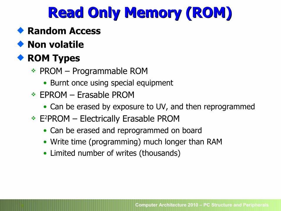
Read Only Memory (ROM)Read Only Memory (ROM)◆ Random Access◆ Non volatile◆ ROM Types
PROM – Programmable ROM• Burnt once using special equipment
EPROM – Erasable PROM• Can be erased by exposure to UV, and then reprogrammed
E2PROM – Electrically Erasable PROM• Can be erased and reprogrammed on board• Write time (programming) much longer than RAM• Limited number of writes (thousands)
Computer Architecture 2010 – PC Structure and Peripherals10
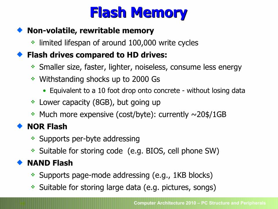
Flash MemoryFlash Memory◆ Non-volatile, rewritable memory
limited lifespan of around 100,000 write cycles◆ Flash drives compared to HD drives:
Smaller size, faster, lighter, noiseless, consume less energy Withstanding shocks up to 2000 Gs
• Equivalent to a 10 foot drop onto concrete - without losing data
Lower capacity (8GB), but going up Much more expensive (cost/byte): currently ~20$/1GB
◆ NOR Flash Supports per-byte addressing Suitable for storing code (e.g. BIOS, cell phone SW)
◆ NAND Flash Supports page-mode addressing (e.g., 1KB blocks) Suitable for storing large data (e.g. pictures, songs)
Computer Architecture 2010 – PC Structure and Peripherals11
The MotherboardThe Motherboard
Computer Architecture 2010 – PC Structure and Peripherals12
Computer System StructureComputer System Structure
CPU
PCI
North BridgeDDRII
Channel 1
mouse
LAN
LanAdap
External Graphics
Card
Mem BUS
Cache
SoundCard
speakers
South Bridge
PCI express ×16
IDEcontroller
IO Controller
Old DVDDrive
HardDisk
Par
alle
l P
ort
Se
rial
Po
rt FloppyDrive
keybrd
DDRIIChannel 2
USBcontroller
SATAcontroller
PCI express ×1
Memory controller
On-board Graphics
CPU BUS
Computer Architecture 2010 – PC Structure and Peripherals13
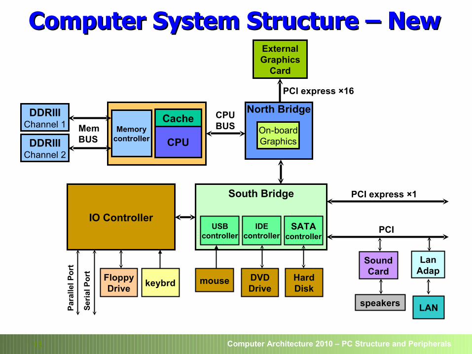
Computer System Structure – NewComputer System Structure – New
PCI
North Bridge
mouse
LAN
LanAdap
External Graphics
Card
CPU BUS
SoundCard
speakers
South Bridge
PCI express ×16
IDEcontroller
IO Controller
DVDDrive
HardDisk
Par
alle
l P
ort
Se
rial
Po
rt FloppyDrive
keybrd
USBcontroller
SATAcontroller
PCI express ×1
On-board GraphicsCPU
CacheDDRIII
Channel 1 Mem BUSDDRIII
Channel 2
Memory controller
Computer Architecture 2010 – PC Structure and Peripherals14
Hard DisksHard Disks
Computer Architecture 2010 – PC Structure and Peripherals15
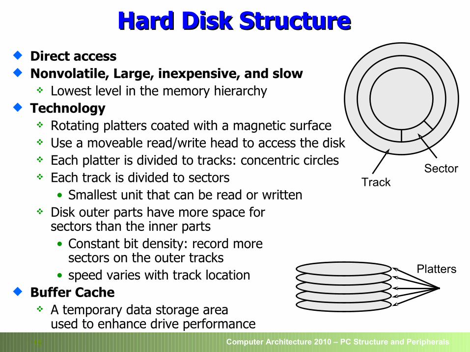
Hard Disk StructureHard Disk Structure◆ Direct access◆ Nonvolatile, Large, inexpensive, and slow
Lowest level in the memory hierarchy◆ Technology
Rotating platters coated with a magnetic surface Use a moveable read/write head to access the disk Each platter is divided to tracks: concentric circles Each track is divided to sectors
• Smallest unit that can be read or written Disk outer parts have more space for
sectors than the inner parts• Constant bit density: record more
sectors on the outer tracks• speed varies with track location
◆ Buffer Cache A temporary data storage area
used to enhance drive performance
Platters
TrackSector
Computer Architecture 2010 – PC Structure and Peripherals16
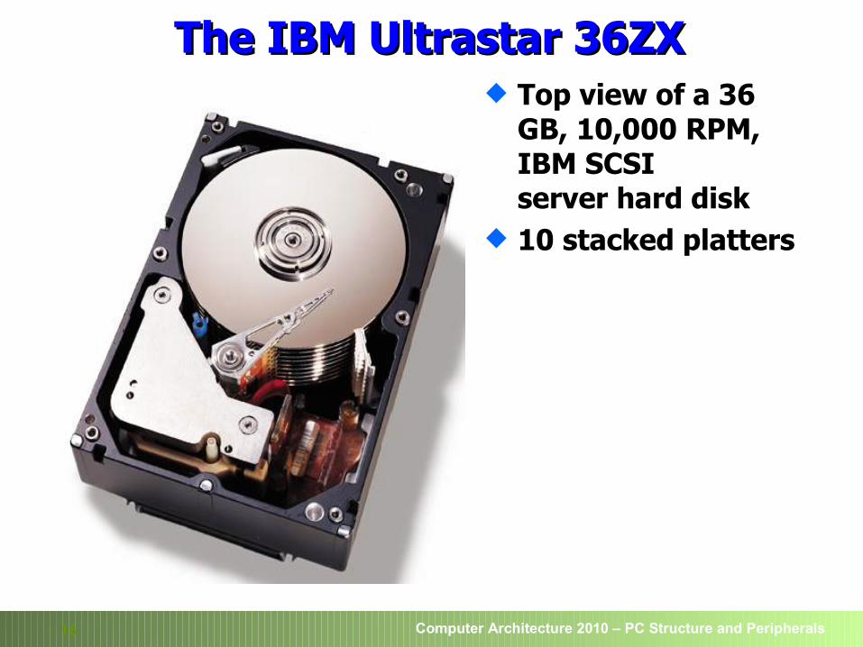
The IBM Ultrastar 36ZXThe IBM Ultrastar 36ZX◆ Top view of a 36
GB, 10,000 RPM, IBM SCSIserver hard disk
◆ 10 stacked platters
Computer Architecture 2010 – PC Structure and Peripherals17
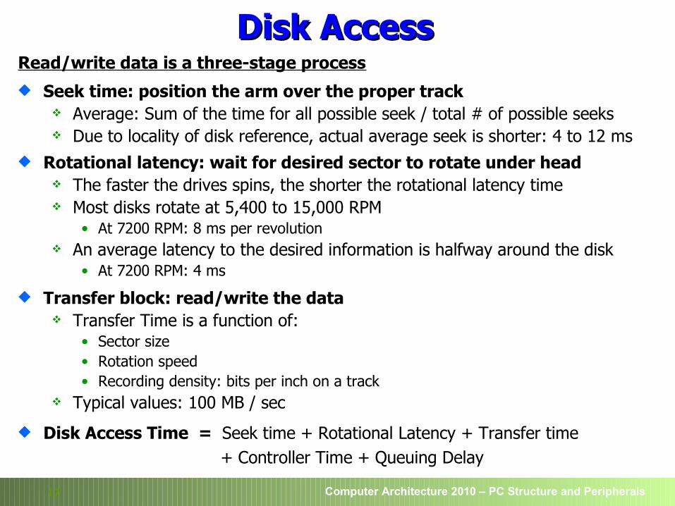
Disk AccessDisk AccessRead/write data is a three-stage process
◆ Seek time: position the arm over the proper track Average: Sum of the time for all possible seek / total # of possible seeks Due to locality of disk reference, actual average seek is shorter: 4 to 12 ms
◆ Rotational latency: wait for desired sector to rotate under head The faster the drives spins, the shorter the rotational latency time Most disks rotate at 5,400 to 15,000 RPM
• At 7200 RPM: 8 ms per revolution An average latency to the desired information is halfway around the disk
• At 7200 RPM: 4 ms
◆ Transfer block: read/write the data Transfer Time is a function of:
• Sector size• Rotation speed• Recording density: bits per inch on a track
Typical values: 100 MB / sec
◆ Disk Access Time = Seek time + Rotational Latency + Transfer time + Controller Time + Queuing Delay
Computer Architecture 2010 – PC Structure and Peripherals18
Solid State Drive – SSDSolid State Drive – SSD◆ Performance numbers used by most manufacturers represent "burst rate"
Not its steady state or average read rate
◆ Any write operation requires an erase followed by the write When SSD is new, NAND flash memory is pre-erased
◆ Consumer-grade multi-level cell (MLC) – allows ≥2 bit per flash memory cell Sustains 2,000 to 10,000 write cycles Notably less expensive than SLC drives
◆ Enterprise-class single-level cell (SLC) – allows 1 bit per flash memory cell Lasts 10× write cycles of an MLC
◆ The more write/erase cycles there are, the shorter the drive's lifespan Wear-leveling algorithms evenly distribute data across flash memory, and move
data around, so that no one portion wears out faster than another• SSD's controller keeps a record of where data is set down on the drive as it is relocated
from one portion to another Add DRAM cache to buffer data writes to reduce the number of write/erase cycles Have extra memory cells; when blocks of flash memory wear out, use spare
blocks
Computer Architecture 2010 – PC Structure and Peripherals19
SSD (cont.)SSD (cont.)◆ Data in NAND flash memory organized in fixed size in blocks
When any portion of the data on the drive is changed• Mark block for deletion in preparation for accommodating the new data• Read current data on the block• Redistribute the old data• Lay down the new data in the old block
Old data is rewritten back Typical write amplification is 15 to 20
• For every 1MB of data written to the drive, 15MB to 20MBs of space is actually needed
• Using write combining reduces write amplification to ~10%
Computer Architecture 2010 – PC Structure and Peripherals20
The BIOSThe BIOS
Computer Architecture 2010 – PC Structure and Peripherals21
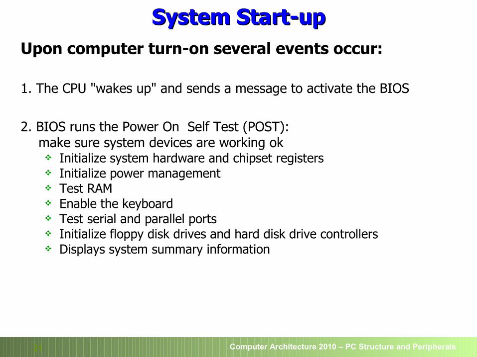
System Start-upSystem Start-upUpon computer turn-on several events occur:
1. The CPU "wakes up" and sends a message to activate the BIOS
2. BIOS runs the Power On Self Test (POST): make sure system devices are working ok Initialize system hardware and chipset registers Initialize power management Test RAM Enable the keyboard Test serial and parallel ports Initialize floppy disk drives and hard disk drive controllers Displays system summary information
Computer Architecture 2010 – PC Structure and Peripherals22
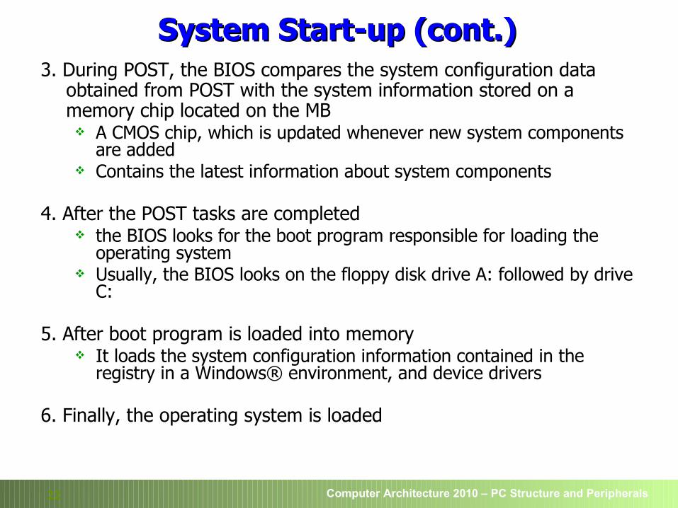
System Start-up (cont.)System Start-up (cont.)3. During POST, the BIOS compares the system configuration data
obtained from POST with the system information stored on a memory chip located on the MB A CMOS chip, which is updated whenever new system components
are added Contains the latest information about system components
4. After the POST tasks are completed the BIOS looks for the boot program responsible for loading the
operating system Usually, the BIOS looks on the floppy disk drive A: followed by drive
C:
5. After boot program is loaded into memory It loads the system configuration information contained in the
registry in a Windows® environment, and device drivers
6. Finally, the operating system is loaded