
PC LAYOUT - asset.conrad.com
12
CLIFF Optical Jacks The CLIFF ® range of Optical Transmitter and Receiver jacks feature seven different models that conform to the EIAJ standard CP-1201 for Digital Audio Interfaces including Fibre-Optical inter- connections. Optical Jacks are virtually unaffected by noise when transmitting and receiving signals between digital audio equipment, enabling high-quality audio recording and high speed signal receiving. It continues to be adopted as a virtual standard in portable audio equipment. Several models have a self-tapping hole for panel mounting and three models replace the plug-in cover with a convenient hinged shutter to protect against contamination. OTJ-2/ORJ-2 Single Optical Transmitter and Receiver Jack. Right angle PCB mount with self tapping hole for panel mounting. Removable plug-in cover. OTJ-2 (FC684202T) ORJ-2 (FC684202R) OTJ-3/ORJ-3 Single Optical Transmitter and Receiver Jack. Right angle PCB mount. Removable plug-in cover. OTJ-3 (FC6842032T) ORJ-3 (FC6842032R) OTJ-4/ORJ-4 Single Optical Transmitter and Receiver Jack. Low profile right angle PCB mount. OTJ-4 (FC684204T) ORJ-4 (FC684204R) OTJ-1/ORJ-1 Single Optical Transmitter and Receiver Jack. Right angle PCB mount with self tapping hole for panel mounting. Removable plug-in cover. OTJ-1 (FC6842031T) ORJ-1 (FC6842031R) PC LAYOUT PC LAYOUT PC LAYOUT PC LAYOUT Cliff Electronic Components, Ltd. 76 Holmethorpe Avenue, Holmethorpe Ind. Est. Redhill, Surrey RH1 2PF. England Tel: +44 (0) 1737 771375 Fax: +44 (0) 1737 766012 Email: [email protected] Visit us online at: www.cliffuk.co.uk
Transcript of PC LAYOUT - asset.conrad.com

CLIFF Optical Jacks
The CLIFF® range of Optical Transmitter and Receiver jacks feature seven different models thatconform to the EIAJ standard CP-1201 for Digital Audio Interfaces including Fibre-Optical inter-connections. Optical Jacks are virtually unaffected by noise when transmitting and receivingsignals between digital audio equipment, enabling high-quality audio recording and high speedsignal receiving. It continues to be adopted as a virtual standard in portable audio equipment.Several models have a self-tapping hole for panel mounting and three models replace the plug-incover with a convenient hinged shutter to protect against contamination.
OTJ-2/ORJ-2 SingleOptical Transmitter andReceiver Jack. Rightangle PCB mount withself tapping hole forpanel mounting.Removable plug-in cover.
OTJ-2 (FC684202T)ORJ-2 (FC684202R)
OTJ-3/ORJ-3 SingleOptical Transmitter andReceiver Jack. Rightangle PCB mount.Removable plug-in cover.
OTJ-3 (FC6842032T)ORJ-3 (FC6842032R)
OTJ-4/ORJ-4 SingleOptical Transmitter andReceiver Jack. Lowprofile right angle PCBmount.
OTJ-4 (FC684204T)ORJ-4 (FC684204R)
OTJ-1/ORJ-1 SingleOptical Transmitter andReceiver Jack. Rightangle PCB mount withself tapping hole forpanel mounting.Removable plug-in cover.
OTJ-1 (FC6842031T)ORJ-1 (FC6842031R)
PC LAYOUT
PC LAYOUT
PC LAYOUT
PC LAYOUT
Cliff Electronic Components, Ltd.76 Holmethorpe Avenue, Holmethorpe Ind. Est.
Redhill, Surrey RH1 2PF. England Tel: +44 (0) 1737 771375 Fax: +44 (0) 1737 766012Email: [email protected]
Visit us online at:
w w w. c l i f f u k . c o . u k

CLIFF Optical Jacks
OTJ-6/ORJ-6 Dual SPDIFRCA and OpticalTransmitter and ReceiverJack. Right angle PCBmount with self tappinghole for panel mounting.Hinged shutter. Severaldifferent colored insertsavailable.
OTJ-6 (FC684206T)ORJ-6 (FC684206R)
OTJ-5/ORJ-5 SingleOptical Transmitter andReceiver Jack. Rightangle PCB mount withself tapping hole forpanel mounting. Hingedshutter.
OTJ-5 (FC684205T)ORJ-5 (FC684205R)
Electrical Specifications: Supply Voltage: -0.5 to 7.0V Maximum.Input Voltage: -0.5 to +0.5V Maximum.Operating Temperature: -20 deg. C to +70 deg. C Maximum.Storage Temperature: -30 deg. C to +80 deg. C Maximum.Soldering Temperature: 260 deg. C Maximum.
Mechanical Specifications: Insertion Force: 5.9N Minimum, 39.2N Maximum.Withdrawal Force: 5.9N Minimum, 39.2N Maximum.
Materials: Body: PBT +30G, ABS 94-V-0 (depends on model)Shutter: Nylon PA66
Please refer to the individual technical data sheets available for each model for the recommendedoperating conditions, characteristics, PC layouts and technical information. We also manufacturemolded optical lead assemblies for use with our optical jacks. Please contact our sales office formore details.
PC LAYOUT
PC LAYOUT
OTJ-8/ORJ-8 OpticalTransmitter and ReceiverJack. Right angle PCBmount. Hinged shutter.
OTJ-8 (FC684208T)ORJ-8 (FC684208R)
PC LAYOUT
2003
CLIF
F®
c
Drawings available on request. Contact [email protected]

FC684208R
SPECIFICATION
CUSTOMER MODEL NO. / TITLE
OPTICAL RECEIVING JACK
(0802R, 0803R, 0807R, 0808R)
Fiber optic receiving module for digital audio interface and navigation system.
Features:
(1) Conform to EIAJ standard CP-1201 (for Digital Audio interfaces Including Fiber Optical
inter-connectors).
(2) A self-tapping hole for easy attachment to Audio Equipments panels.
(3) High speed signal receiving
(12.5Mbps NRZ signal)
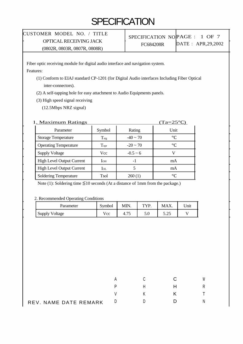
1. Maximum Ratings (Ta=25℃)
Parameter
Storage Temperature
Operating Temperature
Supply Voltage
High Level Output Current
High Level Output Current
Soldering Temperature
Note (1): Soldering time ≦10 seconds (At a distance of 1mm from the package.)
2. Recommended Operating Conditions
Parameter
Supply Voltage
W
R
T
N
Cliff Electronic Components Ltd.
Symbol
Tstg
Topr
Vcc
IOH
IOL
Tsol
Symbol
Vcc
A
P
V
D
SPECIFICATION NO.
FC684208R
Rating
-40 ~ 70
-20 ~ 70
-0.5 ~ 6
260 (1)
MIN.
4.75
-1
5
TYP.
5.0
C
H
K
D
Unit
MAX.
5.25
mA
mA
℃
℃
℃
V
C
H
K
D
PAGE: 1 OF 7
DATE: APR,29,2002
Unit
V
REV. NAME DATE REMARK

SPECIFICATION
CUSTOMER MODEL NO. / TITLE
OPTICAL RECEIVING JACK
3. Optical-electro Characteristics (Ta = 25℃, Vcc = 5V)
Parameter
Data Rate
Transmission Distance
Pulse Width Distortion (4) ∆tw
Maximum Receivable Power
Minimum Receivable Power
Current Consumption
High Level Output Voltage
Low Level Output Voltage
Rise time
Fall time
Low→High delay time
High→Low delay time
Note (2): When non-modulated signal (optical all high or all low level signal) is inputted, output
signal is not stable.
When modulated optical high level signal is received, output signal is high.
When modulated optical low level signal is received, output signal is low.
The duty factor must be maintained between 25 to 75%.
Note (3): All Plastic Fiber (970 / 1000µm).
Note (4): Between input of transmitting module and output of OC0802T.
4. Mechanical Characteristics (Ta= 25℃)
Parameter
Insertion Force.
Withdrawal Force.
Torque for Self-Tap
A
P
V
D
M
ns
mA
V
ns
ns
ns
ns
W
R
T
N
Cliff Electronic Components Ltd.
Using CLIFF OC-0801P,
Initial value
Using self-tapping Screw (TP3×8)
Symbol
PM AX 12.5Mb/s,UsingAPF
PMIN 12.5Mb/s,UsingAPF -24 -
ICC
VOH
VOL
tr
tf
tpLH Refer to “Test Circuit”
tpHL Refer to “Test Circuit”
Condition
NRZ Code (2)
Using APF (3), Using
OC0802T
Pulse Width = 147ns
Pulse Cycle = 294ns
CL = 10pF
Using OC0802T
Refer to “Test Circuit”
Refer to “Test Circuit”
SPECIFICATION NO.
FC684208R
Conditions
C
H
K
D
MIN. TYP. MAX. Unit
58.8
-
5.9
MIN. TYP. MAX. Unit.
0.1
0.2
-15
-
-
2.4 4.8 Vcc V
-
-
-
-
-
-
-
-
C
H
K
D
PAGE: 2 OF 7
DATE: APR,29,2002
-
-
-
- -14.5 dBm
15
0.2
10
10
100
100
39.2
39.2
78.4 N.cm
12.5 Mb/s
180
180
5
15
- dBm
40
0.4
20
20
N
N
REV. NAME DATE REMARK
SPECIFICATION
CUSTOMER MODEL NO. / TITLE
OPTICAL RECEIVING JACK
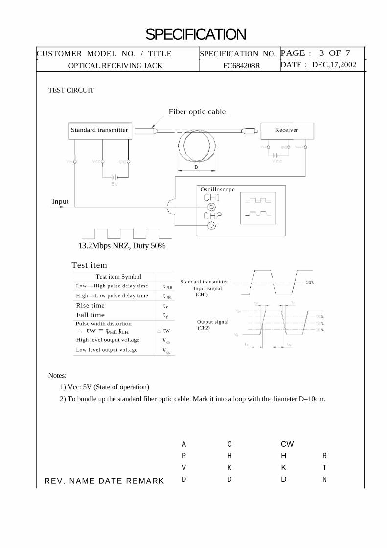
TEST CIRCUIT
Fiber optic cable
Standard transmitter
D
Oscilloscope
Input
13.2Mbps NRZ, Duty 50%
Test item
Test item Symbol
Low High pulse delay time
High Low pulse delay time
Rise time
Fall time
Pulse width distortion
PHL PLH
V
Low level output voltage
Notes:
1) Vcc: 5V (State of operation)
2) To bundle up the standard fiber optic cable. Mark it into a loop with the diameter D=10cm.
W
R
T
N
Cliff Electronic Components Ltd.
tw = t - t
High level output voltage
t
t
t
t
tw
V
r
f
PLH
PHL
OH
OL
Standard transmitter
A
P
V
D
Input signal
(CH1)
SPECIFICATION NO.
FC684208R
Output signal
(CH2)
C
H
K
D
C
H
K
D
Receiver
PAGE: 3 OF 7
DATE: DEC,17,2002
REV. NAME DATE REMARK

SPECIFICATION
CUSTOMER MODEL NO. / TITLE
OPTICAL RECEIVING JACK
5. Application Circuit
Fiber optic connector insertion side
Fiber Optic Receiving Module
1
Less than 7 mm
0.1µF
Vcc
( Bottom View )
6. Required Optical Fiber with Fiber Optic Connectors
OC-0801P
W
R
T
N
Cliff Electronic Components Ltd.
A
P
V
D
SPECIFICATION NO.
FC684208R
GND
2
C
H
K
D
3
Vout
C
H
K
D
PAGE: 4 OF 7
DATE: APR,29,2002
REV. NAME DATE REMARK

.
SPECIFICATION
CUSTOMER MODEL NO. / TITLE
OPTICAL RECEIVING JACK
7. Precautions on Use
(1) Maximum rating
The maximum ratings are the limit values which must not be exceeded during operation of device.
None of these rating value must not be exceeded. If the maximum rating value is exceeded, the
characteristics of devices may never be restored properly. In extreme cases, the device may be
permanently damaged.
(2) Soldering
Optical modules are comprised of internal semiconductor devices. However, in principle, optical
modules are optical components. During soldering, ensure that flux does not contact with the
emitting surface or the detecting surface. Also ensure that proper flux removal is conducted after
soldering.
Some optical modules come with a protective cap. The protective cap is used to avoid malfunction
when the optical module is not in use. Note that it is not dust or waterproof.
As mentioned before, optical modules are optical components. Thus, in principle, soldering where
there may be flux residue and flux removal after soldering is not recommended. Cliff
recommend that soldering be performed without the optical module mounted on the board.
Then, after the board has been cleaned, the optical module should be soldered on to the board manually.
If the optical module cannot be soldered manually, use non-halogen (chlorine-free) flux and make
sure, without cleaning, there is no residue such as chlorine. This is one of the ways to eliminate the
effects of flux. In such a cases, be sure to check the devices‟ reliability.
(3) Noise resistance
It is believed that the use of optical transfer devices improve noise resistance. In theory, optical
fiber is not affected by noise at all. However, receiving modules which handle signals whose level
is extremely small, are susceptible to noise.
The optical module is to be used in an area which is susceptible to radiated noise, increase the shielding by
covering the optical module and the power line filter with a metallic cover.
W
R
T
N
Cliff Electronic Components Ltd
A
P
V
D
SPECIFICATION NO.
FC684208R
C
H
K
D
C
H
K
D
PAGE: 5 OF 7
DATE: APR,29,2002
REV. NAME
DATE REMARK

SPECIFICATION
CUSTOMER MODEL NO. / TITLE
OPTICAL RECEIVING JACK
(4) Vibration and shock
This module is plastic sealed and has its wire fixed by resin. This structure is relatively resistant to
vibration and shock. In actual equipment, there are sometime cases in which vibration, shock, or
stress is applied to soldered parts or connected parts, resulting in lines cut.
Care must be taken in the design of equipment which will be subject to high levels of vibration.
(5) Support pins
The OC0802R has support pins in order to fix itself to the PCB temporary. Please make the hole
for these pins in the PCB under the condition described in board layout hole pattern.
(6) Panel attachment
OC0802R has hole for panel attachment. Please be sure to attach it to panel with self-tapping
screw.
(7) Solvent
When using solvent for flux removal, do not use a high acid or high alkali solvent. Be careful not
to pour solvent in to the optical connector ports. If solvent is inadvertently poured in to them, clean
it off using cotton tips.
(8) Supply voltage
Use the supply voltage within the recommended operating condition (Vcc = 5±0.25V). Make sure
that supply voltage does not exceed the maximum rating value of 7V, even for an instant.
(9) Interface
The OC0802R has a TTL interface. It can be interfaced with any TTL-compatible C-MOS IC.
(10) Output
If the receiver output is at low and is connected to the power supply, or if the output is high and is
connected to GND, the internal IC may be destroyed.
(11) Soldering condition
Solder at 260℃ or less for no more than ten seconds.
W
R
T
N
Cliff Electronic Components Ltd.
A
P
V
D
SPECIFICATION NO.
FC684208R
C
H
K
D
C
H
K
D
PAGE: 6 OF 7
DATE: APR,29,2002
REV. NAME DATE REMARK

SPECIFICATION
CUSTOMER MODEL NO. / TITLE
OPTICAL RECEIVING JACK
(12) Precautions when disposing of devices and packing materials.
When disposing devices and packing materials, follow the procedures stipulated by local
regulations in order to protect the environment against contamination.
(13) Precautions during use
CLIFF is continually working to improve the quality and the reliability of their products.
Nevertheless, semiconductor devices in general can malfunction or fail due to their inherent
electrical sensitivity and their vulnerability to physical stress. It is the responsibility of the buyer,
when utilizing CLIFF products, to observe standards of safety, and to avoid situations in which
the malfunction or failure of a CLIFF product could cause loss of human life, bodily injury or
damage to property.
Mating plug
W
R
T
N
Cliff Electronic Components Ltd.
A
P
V
D
SPECIFICATION NO.
FC684208R
C
H
K
D
C
H
K
D
PAGE: 7 OF 7
DATE: APR,29,2002
REV. NAME DATE REMARK

Document No.
01-E
1. This part should not contain any substances which are specified in follow .(Except
cadmium is less than 5ppm, Lead is under 90ppm)
2. In this case, pre-processing methods and measurement methods shall conform to ROHS.
3. List of “Environment-related Substances to be Controlled („The Controlled Substances‟)”
Substances
Cadmium and cadmium compounds
Heavy metals
Mercury and mercury compounds
Hexavalent chromium compounds
Polychlorinated biphenyls (PCB)
Chlorinated organic
compounds
Mirex (Perchlordecone)
Other chlorinated organic compounds
Polybrominated biphenyls (PBB)
Brominated organic
compounds
Other brominated organic compounds
Organic tin compounds (tributy tin compounds, Triphenyl tin compounds)
Asbestos
Azo compounds
Formaldehyde
Polyvinyl chloride (PVC) and PVC blends
4. Allowable concentrations:
Less than 90ppm is determined as an allowable total-concentration of four heavy metals
(mercury, cadmium, hexavalent chromium, and lead). Less than 5ppm is determined as an
allowable cadmium-concentration in a plastic (including rubber) part.
REV. NAME DATE REMARK
Cliff Electronic Components Ltd.
Management standards for “Environment-related
substances to be controlled”
Document name
Lead and lead compounds
Lead in the plastic,rubber,paints,ink
Polychlorinated naphthalenes (PCN)
Chlorinated paraffins (CP)
Polybrominated diphenylethers (PBDE)
Tetrabromobisphenol-A-bis- (2, 3-dibromopropylether) (TBBP-A-bis)
A
P
V
D
C
H
K
D
C
H
K
D
Rev.
1.6 OCT,26,2006
Allowable
concentration
Less 5ppm
Less 90ppm
Less 50ppm
W
R
T
N
DATE

QMFZ2 Component - Plastics
E I DUPONT DE NEMOURS & CO INC
ENGINEERING POLYMERS CHESTNUT RUN PLAZA PO BOX 80713 WILMINGTON DE 19880
Material Designation: 70G33L(+)
Product Description: Polyamide 66 (PA66), glass reinforced, designated "Zytel" furnished as pellets.
Color
ALL
1.5
3.0
CTI: 0
(+)
NOTE
"MIN".
Report Date: 08/06/1996
120
120
120
130
130
130
IEC BP: -
-
-
-
E41938
IEC GWFI
-
-
-
324299147
UL94 small-scale test data does not pertain to building materials, furnishings and related contents. UL 94 small-scale test data is intended solely for determining the
flammability of plastic materials used in components and parts of end-product devices and appliances, where the acceptability of the combination is determined by ULI.
Min. Thick. (mm)
Virgin and Regrind up to 50% by weight inclusive, have the same basic material characteristics.
(1) Material designations that are color pigmented may be followed by suffix letters and numbers. (2) Material designations may be prefixed by "ZYT" or
0.71
Flame Class
HB
HB
HB
HWI
4
4
4
HVTR: 1
Underwriters Laboratories Inc®
HAI RTI Elec RTI Imp RTI Str IEC GWIT
Thursday, January 16, 2003
0
0
0
130
130
130
D495: 5


