Paulo MoreiraInverter1 The CMOS inverter. Paulo MoreiraInverter2 The CMOS inverter.
10
Paulo Moreira Inverter 1 The CMOS inverter V DD V SS A Y p-switch V DD n-switch V SS A Y A Y 0 good 1 1 good 0
-
date post
20-Dec-2015 -
Category
Documents
-
view
230 -
download
3
Transcript of Paulo MoreiraInverter1 The CMOS inverter. Paulo MoreiraInverter2 The CMOS inverter.
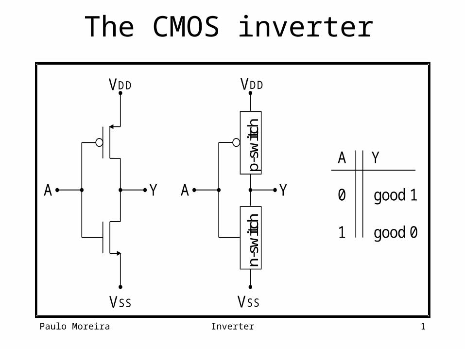
Paulo Moreira Inverter 1
The CMOS inverter
VDD
VSS
A Y
p-sw
itch
VDD
n-sw
itch
VSS
A Y
A Y
0 good 1
1 good 0

Paulo Moreira Inverter 2
The CMOS inverter
0 0.5 1 1.5 2 2.5
0
0.5
1
1.5
2
2.5
Inverter DC transfer characteristic
Slope = -1
Slope = -1
Vou
t (V
)
Vin (V)
Vout=Vin
VDD
VSS
A Y
2.5/0.25
/0.25
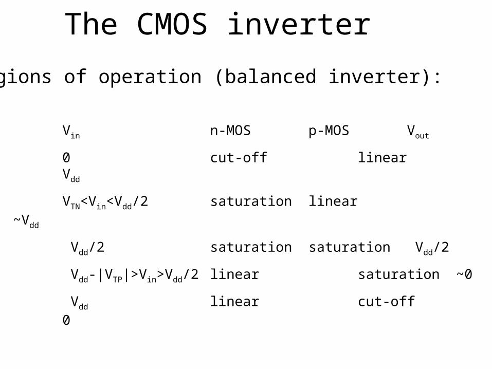
The CMOS inverter Regions of operation (balanced inverter):
Vin n-MOS p-MOS Vout
0 cut-off linear Vdd
VTN<Vin<Vdd/2 saturation linear ~Vdd
Vdd/2 saturation saturation Vdd/2
Vdd-|VTP|>Vin>Vdd/2 linear saturation ~0
Vdd linear cut-off 0
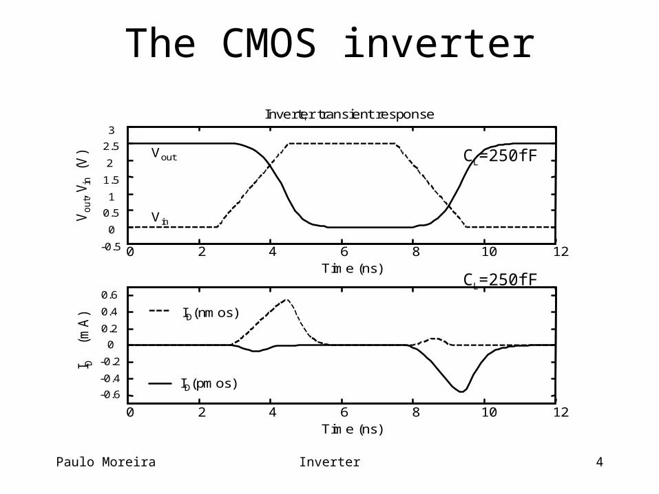
Paulo Moreira Inverter 4
The CMOS inverter
0 2 4 6 8 10 12-0.5
0
0.5
1
1.5
2
2.5
3
Time (ns)
Inverter transient response
0 2 4 6 8 10 12
-0.6
-0.4
-0.2
0
0.2
0.4
0.6
Time (ns)
Vout,
Vin
(V) Vout
Vin
ID(nmos)
ID(pmos)
I D
(m
A)
CL=250fF
CL=250fF
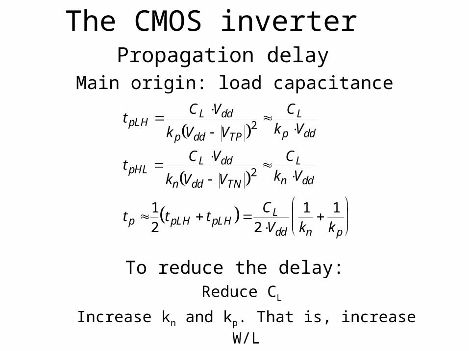
The CMOS inverterPropagation delay
Main origin: load capacitance
To reduce the delay:Reduce CL
Increase kn and kp. That is, increase W/L
tC V
k V V
C
k V
tC V
k V V
C
k V
t t tC
V k k
pLHL dd
p dd TP
L
p dd
pHLL dd
n dd TN
L
n dd
p pLH pLHL
dd n p
2
2
1
2 2
1 1
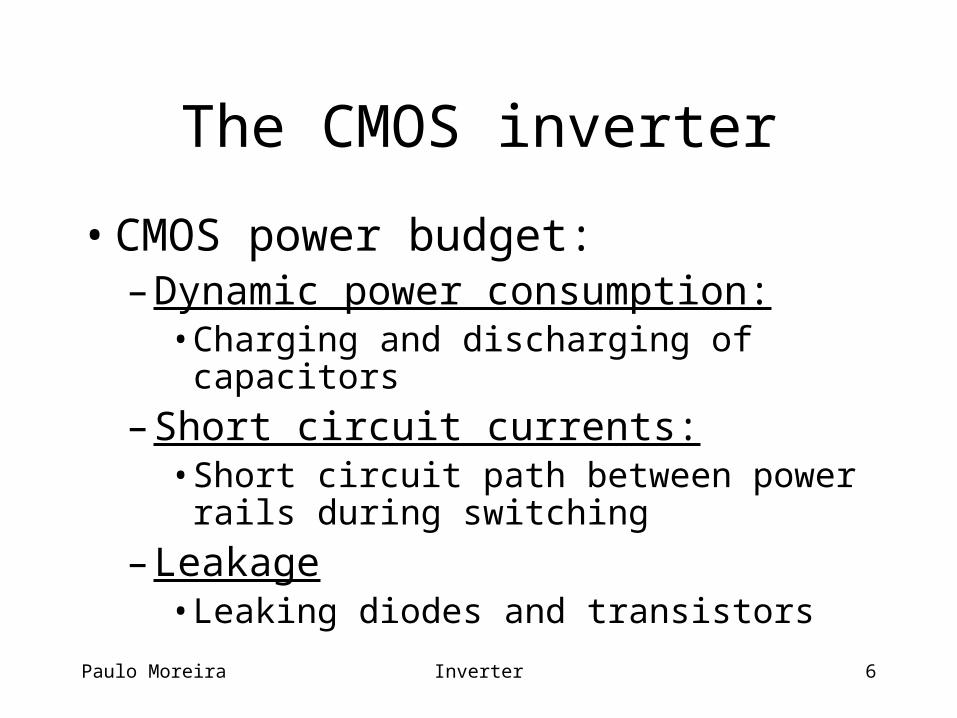
Paulo Moreira Inverter 6
The CMOS inverter
• CMOS power budget:– Dynamic power consumption:
• Charging and discharging of capacitors
– Short circuit currents:• Short circuit path between power rails during
switching
– Leakage• Leaking diodes and transistors
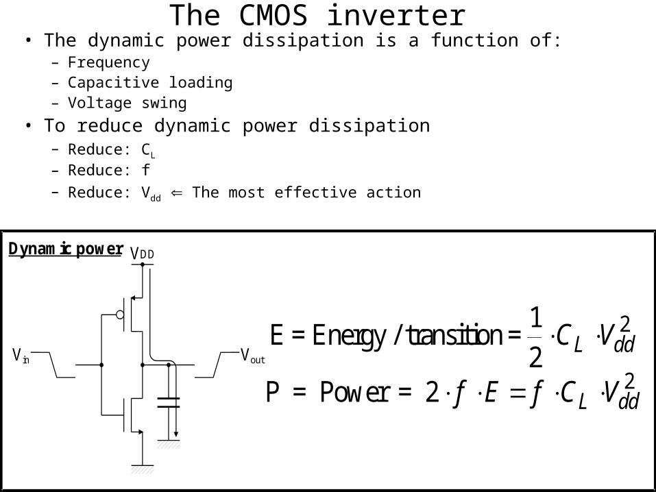
Paulo Moreira Inverter 7
The CMOS inverter• The dynamic power dissipation is a function of:
– Frequency– Capacitive loading– Voltage swing
• To reduce dynamic power dissipation– Reduce: CL
– Reduce: f– Reduce: Vdd The most effective action
VDD
Vin Vout
Dynamic power
E = Energy / transition =
P = Power = 2
1
22
2
C V
f E f C V
L dd
L dd

The CMOS inverter
n+ diffusion metal p+ diffusion
polysiliconn-well
substratecontact (p+) n-well
contact (n+)
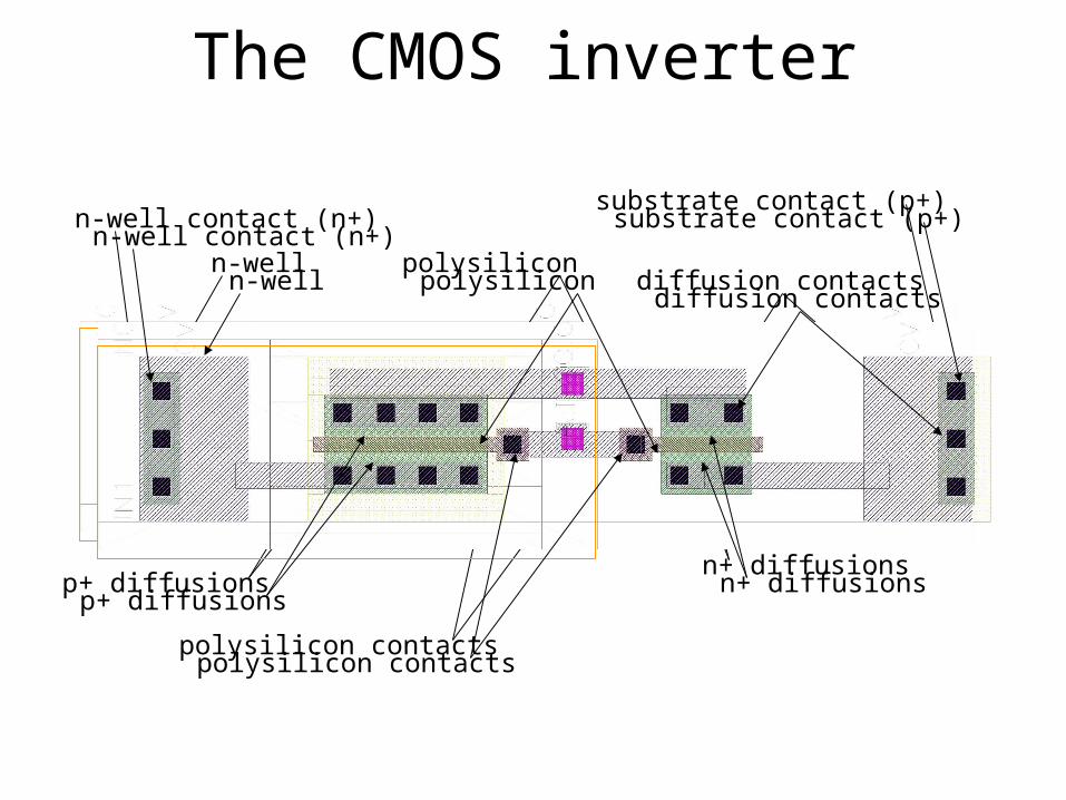
The CMOS inverter
n-well
n-well contact (n+)
p+ diffusions
polysilicon
n+ diffusions
substrate contact (p+)
polysilicon contacts
diffusion contactsn-well
n-well contact (n+)
p+ diffusions
polysilicon
n+ diffusions
substrate contact (p+)
polysilicon contacts
diffusion contacts
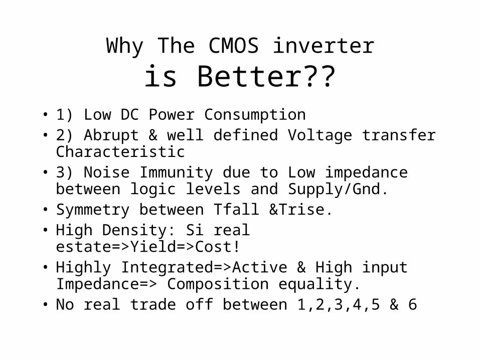
Why The CMOS inverter
is Better??• 1) Low DC Power Consumption• 2) Abrupt & well defined Voltage transfer
Characteristic• 3) Noise Immunity due to Low impedance between
logic levels and Supply/Gnd.• Symmetry between Tfall &Trise.• High Density: Si real estate=>Yield=>Cost!• Highly Integrated=>Active & High input
Impedance=> Composition equality. • No real trade off between 1,2,3,4,5 & 6