Innovative approaches for enhancing the cost-efficiency of ...

Patterning Approaches and System Power EfficiencyConsiderations for Organic LED Displays
J.C. Sturm, F. Pschenitzka, T.R. Hebner, M.H. Lu, C.C. Wu*, and W. Wilson**Center for Photonics and Optoelectronic MateriaIs (POEM)
Department of Electrical Engineering, J-301 E-Quad, Olden St.Princeton University, Princeton, NJ 08544 USA
609-258-5610 fax: 609-258-1954, [email protected]
* present address: ITRI, Hsinchu, Taiwan**present address: Dept. of Physics, University of Utah, Salt Lake City, UT
Keywords: Organic Light Emitting Diodes, OLED's, power efficiency, ink-jetprinting, dry-etching, patterning, full-color, active matrix
Abstract
In this paper we will focus on the various ~sues which reduce the power efficiency ofa complete d~play system vs. that of a single ~olated organic LED, and then discuss theimpact of these ~sues on d~play integration and design. Critical ~sues are the necessityof an active matrix design for high defInition d~plays, and the desire for a power-efficientapproach for full color. Both dry-etching and ink jet printing will be described as optionsfor achieving patterned ftlms.
Introduction
There are now many groups pursing both polymer and small molecule organic light-emitting devices (LED's) for the fabrication of large area d~plays [1-4]. General systemattributes for both types of devices are a high system power efficiency, full color, and low-cost. Although isolated device efficiencies are now over 10 lm/W, the need for highcontrast and the need to individually address pixels in large d~plays can reduce the systempower efficiency to well under 1lrn/W. In this range, we will show that the self-heatingcan be a significant limitation to system performance, even for monochrome displays. Theproblem will be even worse for color displays unless a power-efficient approach towardsfull color can be found. Because patterning organics is attractive for full-color, both dryetching and ink jet pattering approaches will be described.
Self-Heating of Flat Panel Displays
For any future OLED-based flat panel d~play, it is highly desirable that it be cooledpassively, Le. without a fan. Furthermore, for large displays, it is unlikely that heat can beconducted laterally out of the display, but it will have to be dissipated out of the front andback surfaces. The mechanisms for heat transfer from a flat surface to an ambient areradiation and convection. Basic modelling of these mechanisms yielded the results shownin Fig. 1 for the surface heat transfer coefficients for, these mechanisms (k, in W Icm2 per
Part of the SPIE Conference on Oroanic Lioht-Emittino Materials and Devices II
208 San Dieao. California 8 Julv 1998
SPIE Vol. 34768 0277-786X/98/$10.00

degree of temperature difference from the surface to the ambient, l\ T) for verticallyoriented plates. The results for horizontally oriented plates are similar. The details of themodeling and further experiments can be found in Ref. 5. We see that for small plates,convection is efficient, but that it rapidly becomes less efficient as the display size becomeslarger. This is because of the increased distance air must flow across the face of thedisplay. Superimposed on Fig. l(a) are experimental points of measured heat transferefficiencies for vertically oriented square plates, which represent the sum of radiation andconvection. For sizes above 1 cm2, which are those of technological interest for displays,the models well represent the data. At smaller sizes, there is lateral conduction of heatthrough the display, so that the temperature rise is even less than that calculated by one-dimensional models.
0.0035 20~ ' ---OR"".WO ..05 \ ' . ~ . ". 0.003 -Conveclion 1.' .
~ -Tota' 15 .- . .~ 0.0025 . O.ta . .-' -' .''- UII 0.002 t.. 10 0 .a U <I1 0.0015 .
I "horz/v ,~ 5 .' .ho.zltTOfi 0.001 . . '.'II~...:I: . ..,!/fTO
0.0005
00 1 10 100 1000
1 10 100 1000
Display Edgei.o (mm)Displ.y Edge La (mm)
(a) (b)
Figure 1 (a). Surface heat transfer coefficient for convection and radiative (e =0.5) processes for a vertically-oriented display plate, and (b) temperature risevs. edge size for a vertically oriented plate at 220 W Icm2 with two-sided passivecooling.
Fig 1 (b) shows the measured temperature rise in a display as a function of size for afixed power density of 220 W/cm2. Note that the data on the front and back of the plateare similar, and that there is little difference between horizontal and vertical displays. Notethat displays of size -10 cm on an edge have temperature rise nearly an order ofmagnitude larger than that of displays of a size of a few Inm. This is critical because thereliability of OLEO's, which is a critical system concern, is expected to be poorer at highertemperatures [6-9]. Further, most reliability measurements today are made on smalldevices, whereas this data shows that larger displays products will be hotter if operated atthe same brightness (same power density).
Based on the model results shown in Fig 1 (a), a simple relationship between thepower density (PI A) and the temperature rise (l\ To, in K) of a vertical display of edge L(given in meters) with two sided cooling with average emissivity e was developed [5].The expression should be valid for L > 1 cm and for a l\To-L 3 product between 10-4 and
101 K-m3, which encompasses most range of technological interest.
209
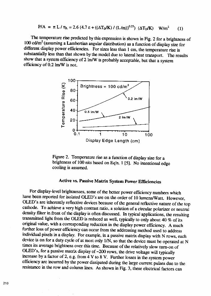
PIA = 1tL/llL= 2.6 (4.7 £+ «ATo/K) I (L/m»o.2s) (ATo/K) W/m2 (1)
The temperature rise predicted by this expression is shown in Fig. 2 for a brightness of100 cd/m2 (assuming a Lambertian angular distribution) as a function of display size fordifferent display power efficiencies. For sizes less than 1 cm, the temperature rise issubstantially less than that shown by the model due to lateral heat transport. The resultsshow that a system efficiency of 2 lm/W is probably acceptable, but that a systemefficiency of 0.2 1m/W is not.
100-~-; 80.~c: 60Q)~
;:,"ca 40~Q)Co
E 20~ - . -
00.1 1 10 100
Display Edge Length (cm)
Figure 2. Temperature rise as a function of display size for abrightness of 100 nits based on Eq'n. 1 [5]. No intentional edgecooling is assumed.
Active vs. Passive Matrix System Power Efficiencies
For display-level brightnesses, some of the better power efficiency numbers whichhave been reported for isolated OLEO's are on the order of 10 lumens/Watt. However,OLEO's are inherently reflective devices because of the general reflective nature of the topcathode. To achieve a very high contrast ratio, a solution of a circular polarizer or neutraldensity filter in front of the display is often discussed. In typical applications, the resultingtransmitted light from the OLEO is reduced as well, typically to only about 40 % of itsoriginal value, with a corresponding reduction in the display power efficiency. A muchfurther loss of power efficiency can occur from the addressing method used to addressindividual pixels in a display. For example, in a passive matrix display with N rows, eachdevice is on for a duty cycle of at most only IIN, so that the device must be operated at Ntimes its average brightness over this time. Because of the relatively slow turn-on ofOLEO's, for a passive matrix display of-200 rows, the drive voltage will typicallyincrease by a factor of 2, e.g. from 4 V to 8 V. Further losses in the system powerefficiency are incurred by the power dissipated during the large current pulses due to theresistance in the row and column lines. As shown in Fig. 3, these electrical factors can
210

easily reduce the efficiency by a factor of 5 for high information content displays. Furtherpower efficiency losses of roughly a factor of two result from the required voltagecompliance on the current drivers which drive the column lines. Taken together, thesefactors can easily reduce the virgin device efficiency of 10 lumen/W to an efficiency for thefinal product of 0.2 lumen/W. Because of system heating considerations, with such asystem efficiency it would be very difficult to build a bright passively-cooled large-scaledisplay.
Pa . Mat' Active Matrixsalve nx
1.0 .f 1.0
I 0.8 100~' ~ 0.8UJ 10Ln.w..DC ~ t t tR_.'5~~ 0.6 D .O06~ 0.6 aVGA VGA t~ '-- Q. SVGA XVGAQ. VGA EE 04 I SVGA ~ 0,4
I =~:~ ::=::: I ~ . t ~ xv i --0.1 nmpixel 100cd'm'
~ ~ (/) 02 --0.3 nmpixel 10 LrTYW in rx;(/) 0.2 t:~-~-:---:=~:= Q)' ,.~ .l, =b.=50cmNsI aVGA =
0000 .. 0 100 200 ~ 400 500 600 700 ~ ~ 0 100 200 ~ 400 500 600 700 000
Nurrj)9r of Rows Number of Rows
(a) (b)
Figure 3. Comparison of decreases in system power efficiency of passive andactive matrix OLED display designs due to electrical considerations for squarepixels of sizes 0.1 and 0.3 mm. A virgin device efficiency of 10 1m/W and abrightness of 100 cd/m2 are assumed. Current source compliance factors in thepassive matrix are not included. Rowand column line sheet resistances are 15.Q/square and 0.05 .Q/square, respectively.
In an active matrix design, a minimum of two transistors per pixel are required forcurrent mode devices such as OLED's. Typically, one functions as a sample and holddevice to capture data from the data line (during the short cycle during which a row isaddressed), and a second transistor is used to translate the stored data into a DC drivecurrent through the OLED. In this way, the high OLED drive voltages, YR drops in rowand column lines, and the problem of DC power dissipation in the column current sourcesin passive matrix displays can be avoided. Some power must be dissipated in thetransistors, however. In a polysilicon TFT process with a mobility» 10 cm2Ns, thisminimum value is set by gray scale resolution effects, and is probably on the order of 1 V(Fig. 3 (b». Combining the effect of a contrast-enhancing plate with the transistor powerdissipation, a system power efficiency of 2-3 lm/W should be achievable, consistent withthe requirements for low self-heating in large-area displays.
Patterning by Dry-Etching
The above calculations of system power efficiencies for passive and active matricesassumed a monochrome display. In practice, color integration may further reduce energy
211

efficiencies, resulting in yet more severe probJems with self heating. For exampJe, onescheme towards full color involves a display of all blue emitters followed by colorconversion modules to convert blue light to green or red light [10]. However, suchconversion processes have an inherent energy inefficiency. An alternate approach wouldfabricate white emitters, with color fIlters to achieve red, green, and blue, an approachwhich would lower energy efficiency by a factor of three. The advantage of theseapproaches is that one needs to make only a single type of OLED. Microcavities can alsobe used to tune the color of a single broadband emitting layer, but have poor propertiesfor off-axis viewing [11]. In principJe, to achieve the ultimate power efficiency for colorintegration, one would want the ability to place individually optimized red, green, and blueemitting devices next to each other on a substrate. This is difficult since both spin-coatingand evaporation produce blanket coatings, and the organic f1lIns are easily damaged byconventional patterning techniques like wet photoresist processing. Furthermore,evaporation of small molecules through a shadow mask is not realistic for a large scaledisplay with many fme pixels.
Therefore we have developed two methods for the pattering of organic films forthe color integration of OLED' s. The first of these is based on dry etching. Previously,we have demonstrated the three color integration of molecular-doped polymer LED's.These were singJe layer devices using PVK doped with both emitting centers (dyes) andelectron transport agents [12,13]. In that work, after the spin-coating of a uniform ftlm, apatterned cathode was evaporated through a shadow mask. The metallic cathode wasthen used as a mask for an oxygen plasma to etch the organic film where it was notprotected by the cathode. The edges of the devices were made electrically inert by apatterned nitride layer deposited before the organic layer. This allowed us to then repeatthe spin-coating process for the next organic layer, which was itself patterned by the samecathode evaporation and dry-etching process. In this way red, green, and blue emitterscould be integrated onto a single substrate [12], with no degradation of the individual
.., 'i
\' ~
...L20 Jlm
T
Figure 4. Aluminum cathode lines (white horizontal lines) patterned byphotolithography and dry-etching on top of PVK on top of ITO lines(vertical).
212

devices due to the integration process. While this work showed the feasibility of etching
organic layers, it still relied on the formation of large-area cathode patterns by shadow-
mask evaporation.
More recently, we have overcome this drawback and developed the ability to
fabricate arbitrary patterns in aluminum-based cathodes on top of polymer films using
photolithographic processing. After the organic layer was spin-coated, a blanket
aluminum-based cathode was deposited by evaporation. Conventional photoresist
patterning was then performed on top of the aluminum, which protected the organic fIlm
from the photoresist processing. To prevent damage to the PVK film during the process,
and to prevent the cathode from peeling from the PVK. it was essential that the cathode
be deposited without any pinholes. The cathode was then dry-etched using a Cl-based
plasma, with no visible damage to the organic layer. Dry-etching was necessary since wet
etching destroyed the structure. Figure 4 shows an aluminum-based cathode which was
patterned by such an etching process (on top of PVK on top of ITO lines patterned by
conventional wet etching). The width of the Allines was 20 ~m and the pitch was 40 ~m.
OLEO's fabricated with such a process had turn-on voltages and quantum efficiencies
similar to those of simultaneously fabricated devices using cathodes defmed by
conventional shadow masks. With the capability to photolithographically defme cathodes
and thus OLEO's to a size« 100 ~m, it should now be possible to integrate optimized R,
G, and B devices within the required pixel sizes for high information content displays.
Patterning by Ink-Jet Printing
As opposed to patterning fIlms after blanket deposition, it is also attractive to consider
the direct patterned deposition of organic fIlms for achieving full color integration. By
using direct patterned deposition, the etching of the organic fIlms could be avoided.
Because polymer fIlms are deposited from solution, in principle they can be deposited in a
local fashion by ink-jet printing, whereby local microdroplets of the polymer solution are
applied to the substrate. We therefore investigated the ink-jet printing of local patterns of
polyvinylcarbazole doped with the dyes of coumarin 47 (C47, blue photoluminescence),coumarin 6 (C6, green), and nile red (orange-red). While in the work presented here the
emitting polymers were directly deposited by ink-jet printing, work has also been done
using ink-jet printing to pattern hole-injecting layers before blanket deposition of the
emitting layers by spin-coating [15].
The work was done using a commercial ink-jet printer designed for printing ink on
paper. It was of the piezoelectric type and had a nozzle opening of 65 microns. The
substrates were 175-~m polyester foils coated with indium tin oxide. The PVK was
dissolved in chloroform at a ratio of about 10 g/1, and the dye concentration was 0.1 g/l.
Using a hand-held syringe, the PVK solution was injected into the ink-reservoir in place of
the usual ink in the printer. We were able to successfully print individual droplets of
polymer using this method [14], although the control of the droplet size was not good.
The droplet size ranged from 150 to 200 urn in diameter, and the height of the polymer
islands ranged from 40 to 70 om. The photoluminescence spectra of the materials
21~

fabricated by inkjet printing were similar to that fabricated by spin-coating (Fig. 5 (a». Aultraviolet-fluorescence image ofa series of letters composed of individual dots dopedwith nile red is shown in Fig. 5 (b). The letters appear "double" because of the "bold" Imode of the printer.
14IPolyester Shee~ PVK 1 . Ink-Jet
12i "'-~ C6
~ "O~I (
= I .:J ,.Q 08
i !
~ /
<I: C47
j 061
~ 041c: 021'E~-J 0,0
400 500 600 700
Wavelength (nm)
(a) (b)
Figure 5. (a) Photoluminescence spectra of PVK films doped with C47, C6,and nile red deposited by both spin-coating and ink-jet printing. Also, (b) UV-fluorescence image of printed letters consisting of dots of PVK doped with nilered. The height of the letters is 3 mrn [14].
0.012 s o 00 pin-on
0 0 00,01 Dink Jet D
0 rJ' D ;0,
~0008 ~ 0 ~N . 0 '
Eo': ~u 0 0
~ 0,000 0 0, Go 00 0"",",Iii ~""a"'1 - ! '0 D 0c: ~ 00004 0' 0Q) ? 0 0
;';11 = , 0=' 0~4 c . <) ~~Or(,' 0002 ~
~I., 0,000
0 2 4 6 8 10 12 14
Voltage M
Figure 6. Current voltage characteristics of OLEO's with 250-~m diameterMg:Ag cathodes on top of 50 nm C6-doped fIlms deposited either by ink-jetprinting (4 devices) or spin-coating (1 device).
It was not possible to fabricate OLEO's on top of individually printed dots due tothe difficulty in placing a cathode on top of a single dot. Therefore to test the quality ofthe ink-jet printed material, the printer was operated in a mode to print a continuous sheetof PVK with a nominal thickness of 50 nm, rather than isolated dots. Cathodes were thenevaporated using standard shadow-mask techniques. The I-V curves of the devices,
~214

along with that of a control device made on a dye-doped PVK [11m fabricated byconventional spin-coating, also with a 50 om thickness, are shown in Fig. 6.
Except for one ink-jet printed device, the turn-on voltage of the two types of deviceswere similar, although the variation in the turn-on voltage of the devices fabricated on ink-jet printed films was substantially larger than that we typically observe in devices in spin-coated films. We think this is due to variations in the thickness of the fIlm deposited byink-jet printing. The quantum efficiency of both types of devices was poor « 0.1 %),probably because no electron transport material was used. When a proper amount of anelectron transport molecule is added to the solution before spin-coating to make a three-component blend, in single-layer spin-coated devices with this material system we typicallyobserve external quantum efficiencies approaching 1 % [13]. Further work is necessary toimprove the fIlm thickness uniformity and also to develop solutions which do not damagethe many plastic parts found in commercial ink jet printers.
Summary
The power efficiency of an OLEO-based display is not only important because ofbattery life in potential applications, but because self-heating of the display may limit theviability itself of the product. There are many considerations which cause the powerefficiency of a complete high definition display system to be far lower than that of anisolated device, and a difference of over a factor of ten can easily result, especially if apassive matrix scheme is adopted. Because of the power dissipation issue, methods forachieving full color without sacrificing power efficiency are important. Both thepatterning of blanket deposited f1lms and cathodes using photolithography and dry-etching, and the direct patterned deposition of polymers using ink-jet printing areattractive alternatives towards this end.
This work was supported by NSF and DARPA.
References
1. C.W. Tang and S.A. Van Slyke, "Organic electroluminescent diodes", Appl. Phys.Lett. 51,913 (1987).
2. J.H. Borroughes, D.D.C. Bradley, AR. Brown, R.N. Marks, R.H. Friend, P.L Bum,and AH. Holmes, "Light-emitting diodes based on conjugated polymers", Nature 347,539 (1990).
3. D. Braun and A.J. Heeger, "Visible light emission from semiconducting polymerdiodes" Appl Phys. Lett. 58, 1982 (1991).
4. C. Adachi, S. Tokito, T. Tsutsui, and S. Saito, "Electroluminescence in organic filmswith three-layer structures", Jap. J. Appl Phys Part 2 Letters, 27, L269 (1988).
5. J.C. Sturm, W. Wilson, and M. Iodice, "Thermal effects and scaling in organic light-emitting flat-panel displays," IEEE J. Set Top. Quant. Elect. 4, 75-82 (1998).
6. S.A. Van Slyke, C.H. Chen, and C.W. Tang, "Organic electroluminescent deviceswith improved stability", Appl Phys. Lett. 69, 2160 (1996).
215
7. I.C. Carter, I. Grizzi, S.K. Heeks et a1, "Operating stability of light-emitting polymerdiodes based on poly(p-phenylene vinylene", AppL Phys. Lett. 71, 34 (1997).
8. P. Burrows, V. Bulovic, S.R. Forrest, L.S. Sapochak, D.M. McCarty, and M.E.Thompson, "Reliability and degradation of organic light emitting devices", AppL Phys.Lett. 65, 2922 (1994).
9. C. Adachi, K Nagai, and N. Tamoto, "Molecular design of hole transport for obtaininghigh durability in organic electroluminescent diodes", AppL Phys. Lett. 66, 2679(1995).
10. C. Hosokawa, M. Eida, M. Matsuura, K. Fukuoka, H. Nakamura, and T. Kusumoto,"Organic Multicolor EL Display with Fine Pixels", Digest of the Society forInformation Display, 1073 (May, 1997).
11. A Dodabalapur, L.I. Rothberg, and T.M. Miller, Electron. Lett 30, 1000 (1994).12. C.C. Wu, I.C. Sturm, and R.A Register, "Integrated three-color organic light-emitting
devices," AppL Phys. Lett. 69, 3117-3119 (1996).13. C.C. Wu, I.C. Sturm, R.A. Register, I. Tian, E.P. Dona, and M.E. Thompson,
"Efficient organic electroluminescent devices using single-layer doped polymer thinfihns with bipolar transport abilities," IEEE Trans. Elec. Dev, 44, 1269-1281 (1997).
14. T.R. Hebner, C.C. Wu, D. Marcy, M.H. Lu, and I.C. Sturm, AppL Phys. Lett 72,519-421 (1998).
15. I. Bharathan and Y. Yang, AppL Phys. Lett. 72, 2660-2662 (1998).