Patterned ferrocenemethanol modified carbon nanotube electrodes on silane modified silicon
5
Patterned ferrocenemethanol modified carbon nanotube electrodes on silane modified silicon Benjamin Scott Flavel, Jingxian Yu, Joseph George Shapter* and Jamie Scott Quinton Received 22nd October 2007, Accepted 23rd October 2007 First published as an Advance Article on the web 29th October 2007 DOI: 10.1039/b716284g Using atomic force anodisation lithography with a silane monolayer as a resist, patterned silicon oxide nanostructures were etched onto a silicon substrate. Condensation reactions were used to immobilise single-walled carbon nanotubes (SWCNT) onto the oxide followed by attachment of ferro- cenemethanol to the nanotubes. These nanostructures are used as electrochemical electrodes to observe oxidation and reduction of ferrocene demonstrating that such controlled nanostructured electrodes are ideal candidates for molecular electronic devices, particularly molecular memory as informa- tion may be stored in discrete redox states. Current device and process scaling in the semiconductor industry has led to a continuous demand for increased density of silicon- based electronics and a decrease in the cost per bit. However, scaling techniques currently employed will soon reach physical and technical limitations 1,2 and alternative methods are now stimulating great interest. One such method is molecular electro- nics which has been proposed to circumvent the limitations associated with current semiconductor devices allowing scaling down to the molecular level 3 whilst dramatically decreasing the associated cost. 1 The field of molecular electronics is very broad. However, two promising approaches are the use of single-walled carbon nano- tubes as interconnects 4,5 and redox-active molecules as a storage medium. 1,6 Carbon nanotubes have attracted considerable interest due to their unique electronic properties such as the high current densities possible and ballistic transport properties making them ideal candidates for molecular scale wires. 5,7 It has been shown by Gooding et al. that carbon nanotubes attached to gold surfaces with alkanethiols allow electrical communication between the underlying electrode surface and redox proteins. 8,9 However, widespread technological application of this approach is uncertain due to issues related to the long-term stability of alkanethiols on gold. 10 Electroactive molecules have stimulated interest as they afford discrete states at distinct voltages. It is therefore possible to store data through the programmed access of the oxidation and reduction states. 1,6 Misra et al. have demonstrated a four state memory element utilising a mixed self assembled monolayer of ferrocene and porphyrin on a silicon substrate. 11 Furthermore, Zhou et al. showed that redox molecules interfaced with a nano- wire can lead to multilevel memory. 12 However, for any molecular electronic approach to be successfully integrated into existing technologies the ability to precisely control the orientation and position of molecular interconnects and storage media is of crucial importance. 6,13 Additionally, construction based on silicon sub- strates will see much more straightforward integration with current architectures. Attempts to address these issues are the subject of this communication. Previously we have demonstrated the assembly of single-walled carbon nanotubes on lithographically patterned silicon/silane substrates 14 and the electron transfer characteristics of carbon nanotubes on unpatterned silicon (100) surfaces. 10,15,16 The investigation in this communication combines these two appro- aches in an attempt to successfully fabricate an electro-active and site selective array of carbon nanotubes. A scanning probe method called anodisation lithography is used to create regions of silicon oxide in a self assembled monolayer of hexadecyltrichlorosilane on silicon substrates, to which single-walled carbon nanotubes with high carboxylic acid functionality are directly attached. The electron transport of this carbon nanotube architecture has then been demonstrated with cyclic voltammetry of redox-active ferrocene in solution. Furthermore, ferrocenemethanol has been attached to the immobilised carbon nanotubes using a condensa- tion reaction between the carboxylic acid groups on the carbon nanotube with the alcohol. Cyclic voltammetry is then repeated in a supporting electrolyte solution demonstrating the potential application for molecular memory. The preparation of the single-walled carbon nanotubes (SWNTs) has been described in detail previously. 14 In brief, SWNTs from Carbon Solutions Inc, California, USA, RFP- SWNT, were refluxed in dilute nitric acid (HNO 3 ) for 24 hours. The dilute nitric acid solution was then removed and the nanotubes were placed into a more aggressive oxidiser, namely a 3 : 1 v/v solution of concentrated sulfuric acid (98%) and concentrated nitric acid (70%) and ultrasonicated for 8 hours at 0 uC. 8,17 The shortened nanotubes were then diluted in 500 mL of ultrapure water and then filtered through a 0.45 mm poly- tetrafluoroethylene (PTFE) filter membrane. The nanotubes were further washed with MilliQ water to bring the pH to 5–7 and dried under vacuum. 8 Atomic force microscope (AFM) images were taken in air using commercially available silicon cantilevers (FESP-ESP) with fundamental resonance frequency between 70 and 85 kHz. Topographic (height) images were obtained. Anodisation litho- graphy was conducted in tapping mode with platinum/iridium coated silicon cantilevers (SCM-PIT) with fundamental resonance frequency between 60 and 75 kHz. Precise movement of the cantilever was controlled using scripts written in C++. All patterns were written with an applied cantilever voltage of 211 V, a tip velocity of 1 mms 21 and an atmospheric humidity level between School of Chemistry, Physics & Earth Sciences, Flinders University, Sturt Road, Bedford Park, Adelaide SA 5001, Australia. E-mail: [email protected]; Tel: +61 (08) 82012005 COMMUNICATION www.rsc.org/materials | Journal of Materials Chemistry This journal is ß The Royal Society of Chemistry 2007 J. Mater. Chem., 2007, 17, 4757–4761 | 4757 Downloaded by Lakehead University on 04 March 2013 Published on 29 October 2007 on http://pubs.rsc.org | doi:10.1039/B716284G View Article Online / Journal Homepage / Table of Contents for this issue
-
Upload
jamie-scott -
Category
Documents
-
view
214 -
download
1
Transcript of Patterned ferrocenemethanol modified carbon nanotube electrodes on silane modified silicon

Patterned ferrocenemethanol modified carbon nanotube electrodes onsilane modified silicon
Benjamin Scott Flavel, Jingxian Yu, Joseph George Shapter* and Jamie Scott Quinton
Received 22nd October 2007, Accepted 23rd October 2007
First published as an Advance Article on the web 29th October 2007
DOI: 10.1039/b716284g
Using atomic force anodisation lithography with a silane
monolayer as a resist, patterned silicon oxide nanostructures
were etched onto a silicon substrate. Condensation reactions
were used to immobilise single-walled carbon nanotubes
(SWCNT) onto the oxide followed by attachment of ferro-
cenemethanol to the nanotubes. These nanostructures are
used as electrochemical electrodes to observe oxidation and
reduction of ferrocene demonstrating that such controlled
nanostructured electrodes are ideal candidates for molecular
electronic devices, particularly molecular memory as informa-
tion may be stored in discrete redox states.
Current device and process scaling in the semiconductor industry
has led to a continuous demand for increased density of silicon-
based electronics and a decrease in the cost per bit. However,
scaling techniques currently employed will soon reach physical
and technical limitations1,2 and alternative methods are now
stimulating great interest. One such method is molecular electro-
nics which has been proposed to circumvent the limitations
associated with current semiconductor devices allowing scaling
down to the molecular level3 whilst dramatically decreasing the
associated cost.1
The field of molecular electronics is very broad. However, two
promising approaches are the use of single-walled carbon nano-
tubes as interconnects4,5 and redox-active molecules as a storage
medium.1,6 Carbon nanotubes have attracted considerable interest
due to their unique electronic properties such as the high current
densities possible and ballistic transport properties making them
ideal candidates for molecular scale wires.5,7 It has been shown by
Gooding et al. that carbon nanotubes attached to gold surfaces
with alkanethiols allow electrical communication between the
underlying electrode surface and redox proteins.8,9 However,
widespread technological application of this approach is
uncertain due to issues related to the long-term stability of
alkanethiols on gold.10
Electroactive molecules have stimulated interest as they afford
discrete states at distinct voltages. It is therefore possible to store
data through the programmed access of the oxidation and
reduction states.1,6 Misra et al. have demonstrated a four state
memory element utilising a mixed self assembled monolayer of
ferrocene and porphyrin on a silicon substrate.11 Furthermore,
Zhou et al. showed that redox molecules interfaced with a nano-
wire can lead to multilevel memory.12 However, for any molecular
electronic approach to be successfully integrated into existing
technologies the ability to precisely control the orientation and
position of molecular interconnects and storage media is of crucial
importance.6,13 Additionally, construction based on silicon sub-
strates will see much more straightforward integration with current
architectures. Attempts to address these issues are the subject of
this communication.
Previously we have demonstrated the assembly of single-walled
carbon nanotubes on lithographically patterned silicon/silane
substrates14 and the electron transfer characteristics of carbon
nanotubes on unpatterned silicon (100) surfaces.10,15,16 The
investigation in this communication combines these two appro-
aches in an attempt to successfully fabricate an electro-active and
site selective array of carbon nanotubes. A scanning probe method
called anodisation lithography is used to create regions of silicon
oxide in a self assembled monolayer of hexadecyltrichlorosilane on
silicon substrates, to which single-walled carbon nanotubes with
high carboxylic acid functionality are directly attached. The
electron transport of this carbon nanotube architecture has then
been demonstrated with cyclic voltammetry of redox-active
ferrocene in solution. Furthermore, ferrocenemethanol has been
attached to the immobilised carbon nanotubes using a condensa-
tion reaction between the carboxylic acid groups on the carbon
nanotube with the alcohol. Cyclic voltammetry is then repeated
in a supporting electrolyte solution demonstrating the potential
application for molecular memory.
The preparation of the single-walled carbon nanotubes
(SWNTs) has been described in detail previously.14 In brief,
SWNTs from Carbon Solutions Inc, California, USA, RFP-
SWNT, were refluxed in dilute nitric acid (HNO3) for 24 hours.
The dilute nitric acid solution was then removed and the
nanotubes were placed into a more aggressive oxidiser, namely
a 3 : 1 v/v solution of concentrated sulfuric acid (98%) and
concentrated nitric acid (70%) and ultrasonicated for 8 hours at
0 uC.8,17 The shortened nanotubes were then diluted in 500 mL
of ultrapure water and then filtered through a 0.45 mm poly-
tetrafluoroethylene (PTFE) filter membrane. The nanotubes were
further washed with MilliQ water to bring the pH to 5–7 and dried
under vacuum.8
Atomic force microscope (AFM) images were taken in air using
commercially available silicon cantilevers (FESP-ESP) with
fundamental resonance frequency between 70 and 85 kHz.
Topographic (height) images were obtained. Anodisation litho-
graphy was conducted in tapping mode with platinum/iridium
coated silicon cantilevers (SCM-PIT) with fundamental resonance
frequency between 60 and 75 kHz. Precise movement of the
cantilever was controlled using scripts written in C++. All patterns
were written with an applied cantilever voltage of 211 V, a tip
velocity of 1 mm s21 and an atmospheric humidity level between
School of Chemistry, Physics & Earth Sciences, Flinders University,Sturt Road, Bedford Park, Adelaide SA 5001, Australia.E-mail: [email protected]; Tel: +61 (08) 82012005
COMMUNICATION www.rsc.org/materials | Journal of Materials Chemistry
This journal is � The Royal Society of Chemistry 2007 J. Mater. Chem., 2007, 17, 4757–4761 | 4757
Dow
nloa
ded
by L
akeh
ead
Uni
vers
ity o
n 04
Mar
ch 2
013
Publ
ishe
d on
29
Oct
ober
200
7 on
http
://pu
bs.r
sc.o
rg |
doi:1
0.10
39/B
7162
84G
View Article Online / Journal Homepage / Table of Contents for this issue

30 and 45%. The tip–substrate distance was reduced prior to
patterning by reducing the amplitude set point to y70% of its
original value. All images presented represent background
subtracted data (using the flatten feature in the WSxM software).18
Highly boron doped p-type silicon (100) with resistivity
,0.001 V cm (Virginia Semiconductor, Inc. USA) was cut into
1 cm 6 1 cm sized wafers and ultrasonically cleaned in acetone for
30 seconds before being thoroughly rinsed with MilliQ water. The
wafers were then cleaned with a 1 : 3 (v/v) mixture of 30% H2O2
and 98% H2SO4, (piranha solution) at 80 uC for 15 minutes
followed by rinsing with MilliQ water. It has been shown that
treatment of silicon with piranha solution affords a highly
hydroxyl terminated silicon surface with a density of approxi-
mately 1015 –OH groups cm22.2 The hydroxyl terminated silicon
wafers were then immersed in a 0.5% solution of 90%
hexadecyltrichlorosilane in hexadecane for 40 minutes, then rinsed
with chloroform and allowed to dry.
Using a method developed in our group,10 carbon nanotubes
were directly attached to the silicon oxide lines created using
anodisation lithography. This process is shown schematically in
Fig. 1. After surface patterning, the silicon wafer was immersed in
a 1 : 1 : 5 solution of 30% NH4OH, 30% H2O2 and MilliQ water
for 15 minutes at 80 uC, thoroughly rinsed with MilliQ water and
blown dry under a stream of ultra-pure nitrogen prior to
immersion into a 1 : 1 : 5 solution of 36% HCl, 30% H2O2 and
MilliQ water for 15 minutes at 80 uC. The sample was then once
again rinsed and dried prior to exposure to carbon nanotube
solution. The now hydroxyl terminated silicon oxide10 pattern was
incubated at 80 uC in a DMSO solution containing N,N9-dicyclo-
hexylcarbodiimide (DCC) and functionalised carbon nanotubes
for 8 hours. Prior to use the carbon nanotube solution was
ultrasonicated for 5 hours to evenly disperse the carbon nanotubes
in solution. Finally the silicon wafer was rinsed in acetone and
allowed to dry. Ferrocenemethanol was then attached to the
carboxylic acid end groups of the carbon nanotubes using another
condensation reaction as shown in the final step of Fig. 1. The
attached carbon nanotube substrate was immersed in 3 mL of a
DMSO solution containing 0.3 mg of N,N9-dicyclohexylcarbodi-
imide and 1.5 mg of ferrocenemethanol (Sigma-Aldrich) for
48 hours at 25 uC. The substrate was then rinsed in acetone and
dried with nitrogen.
Electrochemical measurements were performed with a
BAS100B Electrochemical Analyser (Bioanalytical Systems Inc.,
USA), operating in cyclic voltammetry mode using a specially
designed electrochemical cell. The electrochemical cell has been
described previously10 and is shown schematically in Fig. 2.
Briefly, the underside of the silicon substrate was roughened using
a silicon carbide crystal and adhered to aluminium foil to form the
working electrode. Two different electrochemical experiments
were carried out, one with unmodified carbon nanotube electrodes
and the second with modification as shown in Fig. 2.10 In
the unmodified situation, an electrolyte solution containing
1 mmol L21 ferrocene and 1 mmol L21 tetrabutylammonium
perchlorate (TBAP) in acetonitrile was used. For the ferrocene-
methanol modified carbon nanotube electrodes an electrolyte
solution containing 1 mmol L21 of tetrabutylammonium per-
chlorate in acetonitrile was used. The potential was swept initially
in the anodic direction from 100 to 900 mV at 100 mV s21. The
background capacitive current was subtracted using the UTLIS,
Utilities for Data Analysis software (Dirk Heering).
A requirement of any system to be used in molecular electronics
applications is the important ability to sense and measure current
depending on the electronic state of the system.19 Electrochemical
analysis, namely cyclic voltammetry, which has been used
extensively in the literature,6,11,16,19 was used to probe the ability
of the fabricated carbon nanostructures to conduct electrons and
exhibit distinct states. An AFM image of a carbon nanotube
electrode is shown in Fig. 3 and it can be seen that there is a
relatively small electro-active surface area covered by carbon
nanotubes, which makes it difficult to measure the current from an
individual pattern using the electrochemical setup described. For a
single patterned area of carbon nanotubes, the active surface area
is 4.8 mm2 which is a reduction of active surface area in the order of
105 compared to previous work10 with unpatterned silicon where
the active surface area is 3.84 6 105 mm2. For this reason, the
silicon surface was repeatedly patterned to create an active surface
region of 300 mm2 to increase the current to a level that is
detectable with our electrochemical system. All voltammograms
presented in this paper are the response from a collection of
patterned regions. However, even with repeated patterning the
resultant active electrode surface is still 103 times smaller thanFig. 1 Mechanism for fabrication of a patterned ferrocenemethanol
modified carbon nanotube electrode on silicon (not to scale).
4758 | J. Mater. Chem., 2007, 17, 4757–4761 This journal is � The Royal Society of Chemistry 2007
Dow
nloa
ded
by L
akeh
ead
Uni
vers
ity o
n 04
Mar
ch 2
013
Publ
ishe
d on
29
Oct
ober
200
7 on
http
://pu
bs.r
sc.o
rg |
doi:1
0.10
39/B
7162
84G
View Article Online

unpatterned silicon. This is the reason for the reduction in
electrochemical current compared to the previous work.10
Fig. 4 shows the cyclic voltammograms when the carbon
nanotubes structures were used as the working electrode using a
scan rate of 100 mV s21. For both patterned carbon nanotubes
structures both the raw data and a background subtracted
voltammogram are shown along with the electrochemical response
obtained by placing the cell on a region containing only hexa-
decyltrichlorosilane (i.e. no nanotubes). It can be seen that for
unmodified carbon nanotubes when the electrochemical cell is
placed over a region of silane layer the cyclic voltammogram
displays only capacitive current with no observable redox waves.
This combined with previous work,10,16 where it has been shown
that on unpatterned bare silicon substrates redox behaviour is only
observable upon the attachment of carbon nanotubes, proves
that the observed electrochemical response is attributable to the
patterned carbon nanotubes. For the ferrocenemethanol modified
carbon nanotube structures, other small peaks are observable as
a result of the very sensitive scale used. The origin of these
background peaks is discussed in detail later.
For the directly attached carbon nanotube electrode in an elec-
trolyte solution containing 1 mmol L21 ferrocene and 1 mmol L21
tetrabutylammonium perchlorate in acetonitrile distinct redox
waves can be seen. The anodic and cathodic peak positions were
found from the background subtracted data to be at 619 and
403 mV with peak currents of 8.29 and 29.63 nA respectively.
Compared to previous work on unpatterned silicon, this is an
increased separation of the oxidation and reduction peaks by
84 mV. In the previous work on unpatterned silicon a peak current
of approximately 3 mA was obtained for unmodified carbon
nanotubes10 whereas in this work, in the same cell, a peak current
of 8.29 nA is observed, which is a decrease by a factor of 103 and
corresponds well to the decrease in electrode area. Whilst ideally
the measured electrochemical signal should come from an
individual patterned region much more sensitive electronics would
be required and this work simply provides proof of principle. It
also highlights one of the drawbacks to anodisation lithography in
that it is a relatively slow and serial process,20 which in order to
pattern the surface sufficiently to obtain an electrochemical
response requires a great length of time. The peak separation
observed in the unpatterned case compares well to a gold electrode
in ferrocene solution, where the peaks were found to be at 474
and 596 mV respectively.10 The increased peak separation for the
electrochemistry in the case of the patterned electrode is to be
expected due to the increased oxide layer thickness created from
anodisation lithography. This results in a slower electron transfer
rate and hence greater peak separation.16
The increased separation of redox peaks compared to a gold
working electrode can also be explained in terms of contact area
Fig. 3 AFM images of a patterned carbon nanotube electrode.
Nanotube attachment is directly to the patterned oxide through an
ester linkage.
Fig. 2 Schematic of the specially designed electrochemical cell and the two nanotube surfaces examined.
This journal is � The Royal Society of Chemistry 2007 J. Mater. Chem., 2007, 17, 4757–4761 | 4759
Dow
nloa
ded
by L
akeh
ead
Uni
vers
ity o
n 04
Mar
ch 2
013
Publ
ishe
d on
29
Oct
ober
200
7 on
http
://pu
bs.r
sc.o
rg |
doi:1
0.10
39/B
7162
84G
View Article Online
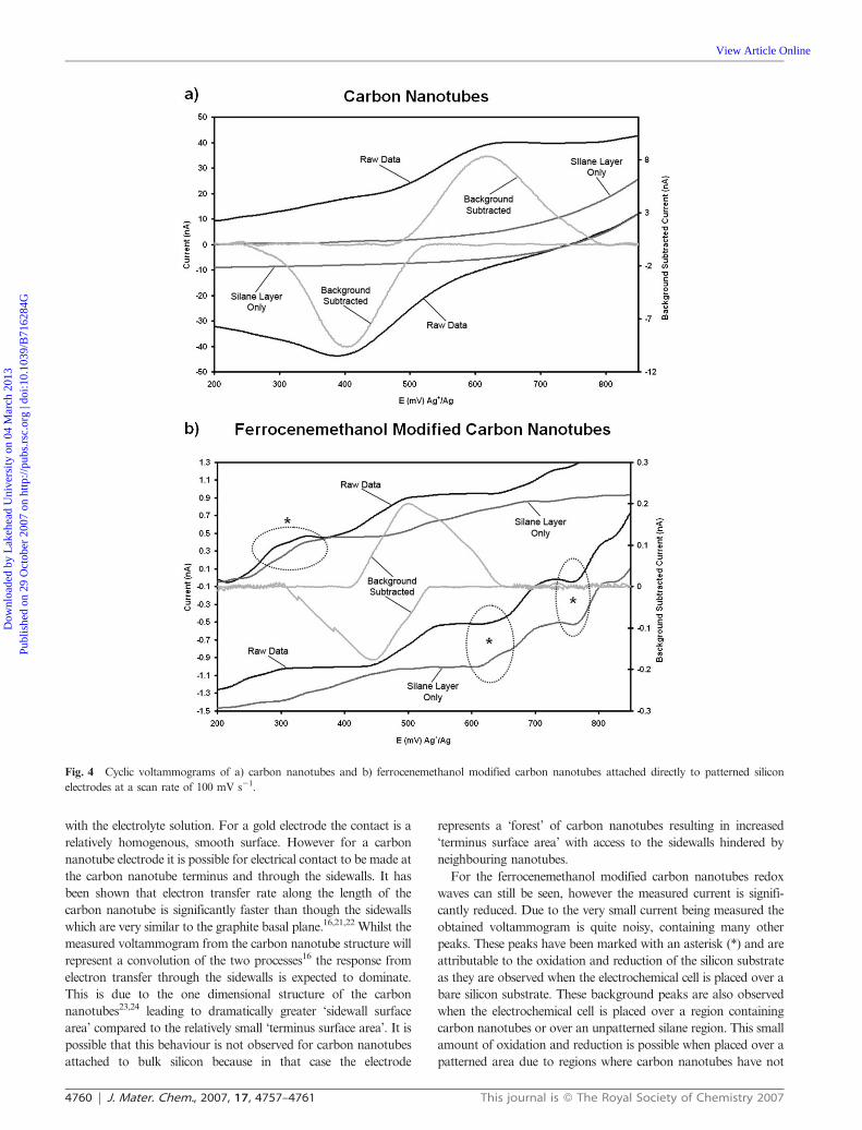
with the electrolyte solution. For a gold electrode the contact is a
relatively homogenous, smooth surface. However for a carbon
nanotube electrode it is possible for electrical contact to be made at
the carbon nanotube terminus and through the sidewalls. It has
been shown that electron transfer rate along the length of the
carbon nanotube is significantly faster than though the sidewalls
which are very similar to the graphite basal plane.16,21,22 Whilst the
measured voltammogram from the carbon nanotube structure will
represent a convolution of the two processes16 the response from
electron transfer through the sidewalls is expected to dominate.
This is due to the one dimensional structure of the carbon
nanotubes23,24 leading to dramatically greater ‘sidewall surface
area’ compared to the relatively small ‘terminus surface area’. It is
possible that this behaviour is not observed for carbon nanotubes
attached to bulk silicon because in that case the electrode
represents a ‘forest’ of carbon nanotubes resulting in increased
‘terminus surface area’ with access to the sidewalls hindered by
neighbouring nanotubes.
For the ferrocenemethanol modified carbon nanotubes redox
waves can still be seen, however the measured current is signifi-
cantly reduced. Due to the very small current being measured the
obtained voltammogram is quite noisy, containing many other
peaks. These peaks have been marked with an asterisk (*) and are
attributable to the oxidation and reduction of the silicon substrate
as they are observed when the electrochemical cell is placed over a
bare silicon substrate. These background peaks are also observed
when the electrochemical cell is placed over a region containing
carbon nanotubes or over an unpatterned silane region. This small
amount of oxidation and reduction is possible when placed over a
patterned area due to regions where carbon nanotubes have not
Fig. 4 Cyclic voltammograms of a) carbon nanotubes and b) ferrocenemethanol modified carbon nanotubes attached directly to patterned silicon
electrodes at a scan rate of 100 mV s21.
4760 | J. Mater. Chem., 2007, 17, 4757–4761 This journal is � The Royal Society of Chemistry 2007
Dow
nloa
ded
by L
akeh
ead
Uni
vers
ity o
n 04
Mar
ch 2
013
Publ
ishe
d on
29
Oct
ober
200
7 on
http
://pu
bs.r
sc.o
rg |
doi:1
0.10
39/B
7162
84G
View Article Online

been attached. In the case of the silane monolayer, oxidation and
reduction is possible through the many pin holes and inhomo-
geneities present in a self assembled silane layer.2
The anodic and cathodic peak positions were found from the
background subtracted data to be at 500 and 444 mV with peak
currents of 0.2 and 20.17 nA respectively. The reduction in
observed current going from ferrocenemethanol in solution to the
case where the redox active molecule is attached is simply due to a
reduction in the amount of available redox molecules which is
much higher for the solution case. AFM imaging of the nanotube
substrate before and after attachment of the ferrocenemethanol
shows no changes in the substrate meaning variation in observed
current is not due to substrate modification.16
It can be seen that upon attaching the electro-active ferrocene-
methanol molecule directly to the carbon nanotube peak
separation decreases by 150 mV compared to the separation
observed for ferrocene in solution over the unmodified carbon
nanotube electrode. This, along with the reduction in current, can
be explained once again by considering the location on the carbon
nanotube from which electron transfer is occurring. It has been
shown that the oxidation of carbon nanotubes with nitric and
sulfuric acid mixtures will introduce carboxyl groups at the highly
reactive end caps of the carbon nanotube.8,15,25,26 Whilst some
carboxyl functionality will exist along the sidewalls from defects
such as the Stone–Wales defect,26 carboxyl groups will predomi-
nately exist on the end caps25,26 and hence it is expected that
significantly more ferrocenemethanol will be immobilised in these
regions. As a result of this most molecular attachment will occur
on the end of the nanotubes meaning that most electron transfer
occurs along the length of the carbon nanotube shifting the
oxidation and reduction peaks towards each other due to the ease
of electron transfer down the length of the nanotube. However, as
the electroactive species are now on such a small surface area, a
decreased current is observed. This decrease in peak separation has
also been observed for modified carbon nanotubes on unpatterned
silicon substrates where the peaks were seen to shift together by
42 mV, yielding a peak separation of 80 mV compared to 122 mV
for unmodified carbon nanotubes.10,16 Upon looking at the
background subtracted voltammogram further it can be seen that
the oxidation and reduction peaks are also quite broad and
possibly even contain some structure at higher peak separations.
We speculate that this could be attributed to ferrocenemethanol
immobilised on the sidewalls through the defect sites previously
discussed which will yield highly separated peaks and hence a
broadened signal.
In summary, this work presents a new approach for the
fabrication of silicon-based molecular electronic devices meeting
the basic requirement that a current can be measured from
spatially defined regions. Whilst the measured electrochemical
currents are quite small and the electron transfer rate is reduced as
a result of the increased oxide thickness from anodisation
lithography, this approach looks promising for future application
as it uses low energy processes for fabrication. In particular the
attachment of redox active molecules such as ferrocenemethanol to
defined carbon nanotube structures has significant potential in the
field of molecular memory.
Notes and references
1 C. Li, J. Ly, B. Lei, W. Fan, D. Zhang, J. Han, M. Meyyappan,M. Thompson and C. Zhou, J. Phys. Chem. B, 2004, 108, 9646.
2 D. K. Aswal, S. Lenfant, D. Guerin, J. V. Yakhmi and D. Vuillaume,Anal. Chim. Acta, 2006, 568, 84.
3 Q. Zhao, Y. Luo, S. Surthi, Q. Li, G. Mathur, S. Gowda, P. R. Larson,M. B. Johnson and V. Misra, Nanotechnology, 2005, 16, 257.
4 S. S. Xie, W. Z. Li, Z. W. Pan, B. H. Chang and L. F. Sun, Eur. Phys. J.D, 1999, 9, 85.
5 J. Liu, M. J. Casavant, M. Cox, D. A. Walters, P. Boul, W. Lu,A. J. Rimberg, K. A. Smith, D. T. Colbert and R. E. Smalley, Chem.Phys. Lett., 1999, 303, 125.
6 Q. Li, G. Mathur, M. Homsi, S. Surthi, V. Misra, V. Malinovskii,K.-H. Schweikart, L. Yu, J. S. Lindsey, Z. Liu, R. B. Dabke, A. Yasseri,D. F. Bocian and W. G. Kuhr, Appl. Phys. Lett., 2002, 81, 1494.
7 Y. Joon Jung, B. Wei, R. Vajtai, P. M. Ajayan, Y. Homma,K. Prabhakaran and T. Ogino, Nano Lett., 2003, 3, 561.
8 J. J. Gooding, R. Wibowo, J. Liu, W. Yang, D. Losic, S. Orbons,F. J. Mearns, J. G. Shapter and D. B. Hibbert, J. Am. Chem. Soc., 2003,125, 9006.
9 J. Liu, A. Chou, W. Rahmat, M. N. Paddon-Row and J. J. Gooding,Electroanalysis, 2005, 17, 38.
10 J. Yu, J. G. Shapter, J. S. Quinton, M. R. Johnston and D. A. Beattie,Phys. Chem. Chem. Phys., 2007, 9, 510.
11 Q. Li, G. Mathur, S. Gowda, S. Surthi, Q. Zhao, L. Yu, J. S. Lindsey,D. F. Bocian and V. Misra, Adv. Mater., 2004, 16, 133.
12 C. Li, W. Fan, B. Lei, D. Zhang, S. Han, T. Tang, X. Liu, Z. Liu,S. Asano, M. Meyyappan, J. Han and C. Zhou, Appl. Phys. Lett., 2004,84, 1949.
13 W. Y. Lee, C. H. Weng, Z. Y. Juang, J. F. Lai, K. C. Leou andC. H. Tsai, Diamond Relat. Mater., 2005, 14, 1852.
14 B. S. Flavel, J. Yu, J. G. Shapter and J. S. Quinton, Carbon, 2007, 45,2551.
15 J. Yu, D. Losic, M. Marshall, T. Bocking, J. J. Gooding andJ. G. Shapter, Soft Matter, 2006, 2, 1081.
16 J. Yu, J. G. Shapter, M. R. Johnston, J. S. Quinton and J. J. Gooding,Electrochim. Acta, 2007, 52, 6206.
17 X. Nan, Z. Gu and Z. Liu, J. Colloid Interface Sci., 2002, 245, 311.18 I. Horcas, R. Fernandez, J. M. Gomez-Rodriguez, J. Colchero,
J. Gomez-Herrero and A. M. Baro, Rev. Sci. Instrum., 2007, 78, 13705.19 R. L. Carroll and C. B. Gorman, Angew. Chem., 2002, 41, 4378.20 Z. P. Huang, D. L. Carnahan, J. Rybczynski, M. Giersig, M. Sennett,
D. Z. Wang, J. G. Wen, K. Kempa and Z. F. Ren, Appl. Phys. Lett.,2003, 82, 460.
21 J. Koehne, J. Li, A. M. Cassell, H. Chen, Q. Ye, H. Tee Ng, J. Han andM. Meyyappan, J. Mater. Chem., 2004, 14, 676.
22 J. Li, A. M. Cassell, L. Delzeit, J. Han and M. Meyyappan, J. Phys.Chem. B, 2002, 106, 9299.
23 Z. J. Zhang, B. Q. Wei, G. Ramanath and P. M. Ajayan, Appl. Phys.Lett., 2000, 77, 3764.
24 V. V. Tsukruk, H. Ko and S. Peleshanko, Phys. Rev. Lett., 2004, 92,65502.
25 H. Kuzmany, A. Kukovecz, F. Simon, M. Holzweber, Ch. Krambergerand T. Pichler, Synth. Met., 2004, 141, 113.
26 J. Zhang, H. Zou, Q. Qing, Y. Yang, Q. Li, Z. Liu, X. Guo and D. Zu,J. Phys. Chem. B, 2003, 107, 3712.
This journal is � The Royal Society of Chemistry 2007 J. Mater. Chem., 2007, 17, 4757–4761 | 4761
Dow
nloa
ded
by L
akeh
ead
Uni
vers
ity o
n 04
Mar
ch 2
013
Publ
ishe
d on
29
Oct
ober
200
7 on
http
://pu
bs.r
sc.o
rg |
doi:1
0.10
39/B
7162
84G
View Article Online