Part Number: Version: Date - Farnell element14SL is not used, this pin should be left open. When...
34
Specification Part Number: Version: Date: Midas Components Limited Electra House 32 Southtown Road Great Yarmouth Norfolk NR31 0DU England Telephone +44 (0)1493 602602 Fax +44 (0)1493 665111 Email [email protected] Website www.midasdisplays.com
Transcript of Part Number: Version: Date - Farnell element14SL is not used, this pin should be left open. When...

SpecificationPart Number:
Version: Date:
Midas Components Limited Electra House 32 Southtown Road Great Yarmouth Norfolk NR31 0DU England
Telephone +44 (0)1493 602602 Fax +44 (0)1493 665111 Email [email protected] Website www.midasdisplays.com
GoodgerR
Stamp
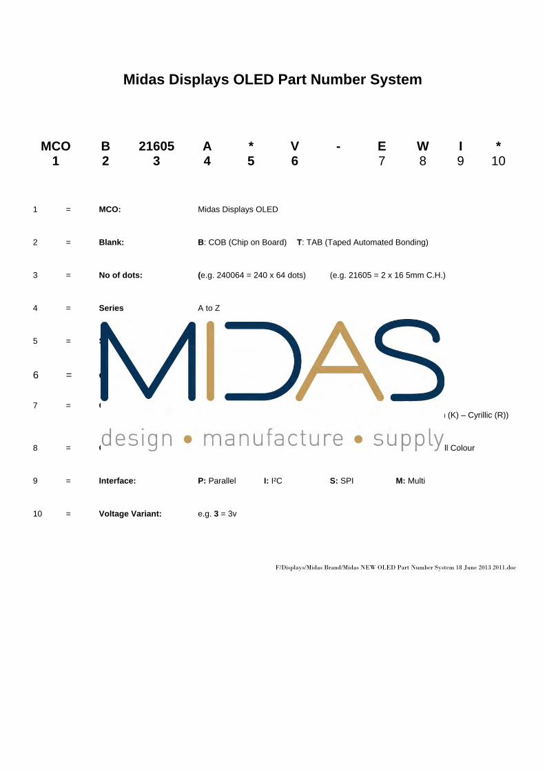
Midas Displays OLED Part Number System
MCO B 21605 A * V - E W I * 1 2 3 4 5 6 7 8 9 10
1 = MCO: Midas Displays OLED
2 = Blank: B: COB (Chip on Board) T: TAB (Taped Automated Bonding)
3 = No of dots: (e.g. 240064 = 240 x 64 dots) (e.g. 21605 = 2 x 16 5mm C.H.)
4 = Series A to Z
5 = Series Variant: A to Z and 1 to 9 – see addendum
6 = Operating Temp Range: A: -30+85° C V: -40+80° C Y: -40 +70° C Z: -30+70° C X: -40 +85° C
7 = Character Set: Blank: Not Applicable E: Multi European Font Set (English/Japanese – Western European (K) – Cyrillic (R))
8 = Colour: Y: Yellow W: White B: Blue R: Red G: Green RGB: Full Colour
9 = Interface: P: Parallel I: I²C S: SPI M: Multi
10 = Voltage Variant: e.g. 3 = 3v
F/Displays/Midas Brand/Midas NEW OLED Part Number System 18 June 2013 2011.doc

i
RReevviisseedd HHiissttoorryy
Part Number Revision Revision Content Revised on
MCOT42005AV-EWM A New September 18, 2012
ii
CCoonntteennttss RReevviissiioonn HHiissttoorryy................................................................................................................................i CCoonntteennttss...........................................................................................................................................ii 11.. BBaassiicc SSppeecciiffiiccaattiioonnss................................................................................................................1~6
1.1 Display Specifications ................................................................................................................. 1 1.2 Mechanical Specifications............................................................................................................ 1 1.3 Active Area / Address Mapping & Character Construction ............................................................... 1 1.4 Mechanical Drawing.................................................................................................................... 2 1.5 Pin Definition ............................................................................................................................. 3 1.6 Block Diagram............................................................................................................................ 5
1.6.1 Low Voltage I/O Application............................................................................................... 5 1.6.2 5V I/O Application ............................................................................................................ 6
22.. AAbbssoolluuttee MMaaxxiimmuumm RRaattiinnggss ........................................................................................................7 33.. Optics & EElleeccttrriiccaall CChhaarraacctteerriissttiiccss .......................................................................................8~13
3.1 Optics Characteristics.................................................................................................................. 8 3.2 DC Characteristics ...................................................................................................................... 8 3.3 AC Characteristics....................................................................................................................... 9
3.3.1 68XX-Series MPU Parallel Interface Timing Characteristics.................................................... 9 3.3.2 80XX-Series MPU Parallel Interface Timing Characteristics.................................................. 11 3.3.3 Serial Interface Timing Characteristics .............................................................................. 12 3.3.4 I2C Interface Timing Characteristics ................................................................................. 13
44.. FFuunnccttiioonnaall SSppeecciiffiiccaattiioonn.....................................................................................................14~22 4.1 Commands .............................................................................................................................. 14 4.2 Power down and Power up Sequence......................................................................................... 14
4.2.1 Power up Sequence ........................................................................................................ 14 4.2.2 Power down Sequence.................................................................................................... 14
4.3 Reset Circuit ............................................................................................................................ 14 4.4 Actual Application Example........................................................................................................ 15
4.4.1 Low Voltage I/O Application............................................................................................. 15 4.4.2 5V I/O Application .......................................................................................................... 17
4.5 Built-in CGROM (Character Generator ROM)................................................................................ 19 4.6 Self-Defined CGRAM (Character Generator RAM)......................................................................... 22
55.. RReelliiaabbiilliittyy ..................................................................................................................................23 5.1 Contents of Reliability Tests ...................................................................................................... 23 5.2 Failure Check Standard ............................................................................................................. 23
66.. OOuuttggooiinngg QQuuaalliittyy CCoonnttrrooll SSppeecciiffiiccaattiioonnss............................................................................24~27 6.1 Environment Required .............................................................................................................. 24 6.2 Sampling Plan .......................................................................................................................... 24 6.3 Criteria & Acceptable Quality Level............................................................................................. 24
6.3.1 Cosmetic Check (Display Off) in Non-Active Area............................................................... 24 6.3.2 Cosmetic Check (Display Off) in Active Area...................................................................... 26 6.3.3 Pattern Check (Display On) in Active Area......................................................................... 27
77.. PPaacckkaaggee SSppeecciiffiiccaattiioonnss..............................................................................................................28 88.. PPrreeccaauuttiioonnss WWhheenn UUssiinngg TThheessee OOEELL DDiissppllaayy MMoodduulleess .......................................................29~31
8.1 Handling Precautions ................................................................................................................ 29 8.2 Storage Precautions.................................................................................................................. 29 8.3 Designing Precautions............................................................................................................... 30

iii
8.4 Precautions when disposing of the OEL display modules .............................................................. 30 8.5 Other Precautions..................................................................................................................... 31
WWaarrrraannttyy ........................................................................................................................................31 NNoottiiccee.............................................................................................................................................31
1
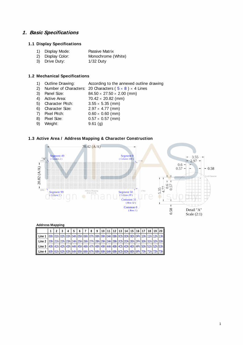
11.. BBaassiicc SSppeecciiffiiccaattiioonnss
1.1 Display Specifications
1) Display Mode: Passive Matrix 2) Display Color: Monochrome (White) 3) Drive Duty: 1/32 Duty
1.2 Mechanical Specifications
1) Outline Drawing: According to the annexed outline drawing 2) Number of Characters: 20 Characters ( 5 × 8 ) × 4 Lines 3) Panel Size: 84.50 × 27.50 × 2.00 (mm) 4) Active Area: 70.42 × 20.82 (mm) 5) Character Pitch: 3.55 × 5.35 (mm) 6) Character Size: 2.97 × 4.77 (mm) 7) Pixel Pitch: 0.60 × 0.60 (mm) 8) Pixel Size: 0.57 × 0.57 (mm) 9) Weight: 9.61 (g)
1.3 Active Area / Address Mapping & Character Construction
(00h)
(60h)
"A"
5 x 8 Character
(73h)
(13h)
70.42 (A/A)
20.8
2 (A
/A) 0.570.6
0.570.6
4.77
5.35
2.973.55
0.58
0.58
Segment 50( Column 99 )
Common 0( Row 1 )
Common 31( Row 32 )
Segment 99( Column 1 )
Segment 0( Column 100 )
Segment 49( Column 2 )
Detail "A"Scale (2:1)
Address Mapping(Full 20 x 4)
Address Mapping
1 2 3 4 5 6 7 8 9 10 11 12 13 14 15 16 17 18 19 20
Line 1 00h 01h 02h 03h 04h 05h 06h 07h 08h 09h 0Ah 0Bh 0Ch 0Dh 0Eh 0Fh 10h 11h 12h 13hLine 2 20h 21h 22h 23h 24h 25h 26h 27h 28h 29h 2Ah 2Bh 2Ch 2Dh 2Eh 2Fh 30h 31h 32h 33h
Line 3 40h 41h 42h 43h 44h 45h 46h 47h 48h 49h 4Ah 4Bh 4Ch 4Dh 4Eh 4Fh 50h 51h 52h 53h
Line 4 60h 61h 62h 63h 64h 65h 66h 67h 68h 69h 6Ah 6Bh 6Ch 6Dh 6Eh 6Fh 70h 71h 72h 73h

±0.3
mm
Unl
ess O
ther
wis
e Sp
ecifi
ed
Uni
t
Tole
ranc
e
Ang
leD
imen
sion
Gen
eral
Rou
ghne
ss
Title
Dat
eB
yD
raw
n
Dra
win
g N
umbe
r
1 of
1Sh
eet
Mat
eria
l
Pane
l / E
.E.
E.
1:1
Scal
eA
3Si
ze
Dat
eIte
mR
emar
k
Rev
.
Soda
Lim
e / P
olyi
mid
e
Cus
tom
er A
ppro
val
Sign
atur
e
±1
B
2012
0309
DM
X20
04SD
GF0
2
Gar
y Li
n
2011
1108
AO
rigin
al D
raw
ing
P.M
.Ti
ng K
uo H
uIv
y Lo
Kat
e C
hung
2±0.1
Pola
rizer
t=0.
2mm
Rem
ove
Tape
t=0.
15m
m M
ax Glu
e
Prot
ectiv
e Ta
pe11
.8x3
.5x0
.05m
m
(Ref
eren
ce M
echn
ical
Des
ign)
(1.8
4) (2.2)
(31.
08)
Det
ail "
A"
Scal
e (2
:1)
0.570.6
0.570.6
4.775.35
2.973.55
0.58
0.58
8
Sym
bol
2 5 76431Pin
1411 1312109 15 16 17 18 19 20 21 22 23 24 25 26 27
N.C
.V
SLV
SSR
EGV
DD
SHLC
SHLS
VD
DV
DD
IOB
S0B
S1B
S2
CS#
RES
#D
/C#
R/W
#(W
R#)
E(R
D#)
D0
D1
D2
D3
D4
D5
D6
D7
IREF
RO
M0
RO
M1
OPR
0O
PR1
VC
OM
HV
CC
N.C
.
28 29 30 31 32
GPI
O
33
Segm
ent 0
( Col
umn
100
)Se
gmen
t 49
( Col
umn
2 )
"A"
Segm
ent 9
9( C
olum
n 1
)Se
gmen
t 50
( Col
umn
99 )
Com
mon
0( R
ow 1
)
Com
mon
31
( Row
32
)
510
8
70.4
2 (A
/A)
72.4
2 (V
/A)
79.5
(Pol
ariz
er)
80.5
±0.2
(Cap
Siz
e)84
.5±0
.2 (P
anel
Siz
e)
(5)
(4)
0.5±
0.5
(118
.3)
32.8
20.82 (A/A)22.82 (V/A)
26.5 (Polarizer)27.5±0.2 (Cap Size)
27.5±0.2 (Panel Size)
(3.34)(2.34)
0.5±0.5
Act
ive
Are
a 2.
89"
20 x
4 C
hara
cter
13.75±0.3
P0.7
0x(3
3-1)
=22.
4±0.
0522
±0.1
(Alig
nmen
t Mar
k)
23.8
±0.2
1.8±0.33.6±0.2
(10)
0.90.1±0.03
W=0
.4±0
.03
10±0.3
2-R0.5
133
N.C.
VSL
VSS
REGVDD
SHLC
SHLS
VDD
VDDIO
BS0
BS1
BS2
CS#
RES#
D/C#
R/W#(WR#)
E(RD#)
D0
D1
D2
D3
D4
D5
D6
D7
IREF
ROM0
ROM1
OPR0
OPR1
VCOMH
VCC
N.C.
GPIO
(7)
(15)
0.1±0.03
Con
tact
Sid
e
Con
tact
Sid
e
B3M
Dou
ble
Side
Tap
et=
0.05
mm
(0.15)
2012
0309
BA
dd D
oubl
e Si
de T
ape
On
FPC
2012
0309
2012
0309
2012
0309
2-R0.5
2-φ0
.8±0.1

3
1.5 Pin Definition
Pin Number Symbol I/O Function
PPoowweerr SSuuppppllyy
7 VDD P
PPoowweerr SSuuppppllyy ffoorr LLooggiicc CCiirrccuuiitt This is a voltage supply pin which is supplied externally or regulated internally. Acapacitor should be connected between this pin and VSS under all circumstances.When internal VDD is disabled, this is a power input pin. It must be connected toVDDIO or external source and always be equal to or lower than VDDIO. (Low Voltage I/O Application) When internal VDD is enabled, it is regulated internally from VDDIO. (5V I/O Application)
8 VDDIO P PPoowweerr SSuuppppllyy ffoorr IInntteerrffaaccee LLooggiicc LLeevveell This is a voltage supply pin. It should match with the MCU interface voltage leveland must be connected to external source
3 VSS P GGrroouunndd ooff OOEELL SSyysstteemm This is a ground pin. It also acts as a reference for the logic pins, the OEL drivingvoltages, and the analog circuits. It must be connected to external ground.
32 VCC P PPoowweerr SSuuppppllyy ffoorr OOEELL PPaanneell This is the most positive voltage supply pin of the chip. It must be connected toexternal source.
DDrriivveerr
26 IREF I CCuurrrreenntt RReeffeerreennccee ffoorr BBrriigghhttnneessss AAddjjuussttmmeenntt This pin is segment current reference pin. A resistor should be connectedbetween this pin and VSS. Set the current at 15μA.
31 VCOMH P VVoollttaaggee OOuuttppuutt HHiigghh LLeevveell ffoorr CCOOMM SSiiggnnaall This pin is the input pin for the voltage output high level for COM signals. Acapacitor should be connected between this pin and VSS.
2 VSL P
VVoollttaaggee OOuuttppuutt LLooww LLeevveell ffoorr SSEEGG SSiiggnnaall This is segment voltage reference pin. When external VSL is not used, this pin should be left open. When external VSL is used, this pin should connect with resistor and diode toground.
EExxtteerrnnaall IICC CCoommmmuunniiccaattiioonn
12 GPIO I/O GGeenneerraall PPuurrppoossee IInnppuutt//OOuuttppuutt This pin could be left open individually or have signal inputted/outputted. It isable to use as the external DC/DC converter circuit enabled/disabled control orother applications.
CCoonnffiigguurraattiioonn
4 REGVDD I
55VV II//OO RReegguullaattoorr CCoonnffiigguurraattiioonn This is internal VDD regulator selection pin in 5V I/O application mode. When this pin is pulled “Low”, internal VDD regulator is disabled. (Low Voltage I/O Application) When this pin is pulled “High”, internal VDD regulator is enabled. (5V I/O Application)
5 SHLC I SSccaannnniinngg DDiirreeccttiioonn ffoorr CCOOMM SSiiggnnaall This pin is used to determine COM output scanning direction. It can still beprogrammable and defined by fundamental command.
6 SHLS I MMaappppiinngg DDiirreeccttiioonn ffoorr SSEEGG SSiiggnnaall This pin is used to change the mapping between the display data column addressand the segment driver. It can still be programmable and defined byfundamental command.
27 28
ROM0 ROM1 I
BBuuiilltt--iinn CChhaarraacctteerr RROOMM SSeelleeccttiioonn These pins are used to select the appropriate character ROM. See the followingtable & Section 4.5:
ROM0 ROM1 ROM A (Page 19) 0 0 ROM B (Page 20) 1 0 ROM C (Page 21) 0 1 Software Selectable 1 1
It can still be programmable and defined by extended command.
4
1.5 Pin Definition (Continued)
Pin Number Symbol I/O Function
CCoonnffiigguurraattiioonn ((CCoonnttiinnuueedd))
29 30
OPR0 OPR1 I
CChhaarraacctteerr RROOMM//RRAAMM MMaannaaggeemmeenntt These pins are used to manage the character number of character generator. Seethe following table & Section 4.6:
CGROM CGRAM OPR0 OPR1 240 8 0 0 248 8 1 0 250 6 0 1 256 0 1 1
It can still be programmable and defined by extended command.
IInntteerrffaaccee
9 10 11
BS0 BS1 BS2
I
CCoommmmuunniiccaattiinngg PPrroottooccooll SSeelleeccttiioonn These pins are MCU interface selection input. See the following table:
BS0 BS1 BS2 I2C 0 1 0 Serial 0 0 0 4-bit 68XX Parallel 1 0 1 4-bit 80XX Parallel 1 1 1 8-bit 68XX Parallel 0 0 1 8-bit 80XX Parallel 0 1 1
14 RES# I PPoowweerr RReesseett ffoorr CCoonnttrroolllleerr aanndd DDrriivveerr This pin is reset signal input. When the pin is low, initialization of the chip isexecuted. Keep this pin pull high during normal operation.
13 CS# I CChhiipp SSeelleecctt This pin is the chip select input. The chip is enabled for MCU communication onlywhen CS# is pulled low.
15 D/C# I
DDaattaa//CCoommmmaanndd CCoonnttrrooll This pin is Data/Command control pin. When the pin is pulled high, the input atD7~D0 will be interpreted as display data. When the pin is pulled low, the inputat D7~D0 will be transferred to the command register. In I2C mode, this pin acts as SA0 for slave address selection. When serial interface mode is selected, this pin must be connected to VSS. For detail relationship to MCU interface signals, please refer to the TimingCharacteristics Diagrams.
17 E/RD# I
RReeaadd//WWrriittee EEnnaabbllee oorr RReeaadd This pin is MCU interface input. When interfacing to a 68XX-seriesmicroprocessor, this pin will be used as the Enable (E) signal. Read/write operationis initiated when this pin is pulled high and the CS# is pulled low. When connecting to an 80XX-microprocessor, this pin receives the Read (RD#)signal. Data read operation is initiated when this pin is pulled low and CS# ispulled low. When serial or I2C mode is selected, this pin must be connected to VSS.
16 R/W# I
RReeaadd//WWrriittee SSeelleecctt oorr WWrriittee This pin is MCU interface input. When interfacing to a 68XX-seriesmicroprocessor, this pin will be used as Read/Write (R/W#) selection input. Pullthis pin to “High” for read mode and pull it to “Low” for write mode. When 80XX interface mode is selected, this pin will be the Write (WR#) input.Data write operation is initiated when this pin is pulled low and the CS# is pulledlow. When serial or I2C mode is selected, this pin must be connected to VSS.
18~25 D0~D7 I/O
HHoosstt DDaattaa IInnppuutt//OOuuttppuutt BBuuss These pins are 8-bit bi-directional data bus to be connected to themicroprocessor’s data bus. When serial mode is selected, D0 will be the serialclock input SCLK; D1 will be the serial data input SID and D2 will be the serial clockoutput SOD. When I2C mode is selected, D2, D1 should be tired together andserve as SDAOUT, SDAIN in application and D0 is the serial clock input, SCL. Unused pins must be connected to VSS.
RReesseerrvvee
1, 33 N.C. (GND) - RReesseerrvveedd PPiinn ((SSuuppppoorrttiinngg PPiinn)) The supporting pins can reduce the influences from stresses on the function pins.These pins must be connected to external ground as the ESD protection circuit.

5
1.6 Block Diagram
1.6.1 Low Voltage I/O Application
Com
mon
31
Segm
ent 5
0
Com
mon
0
Segm
ent 0
Segm
ent 9
9
~ ~ ~ ~ ~ ~
Segm
ent 4
9
Active Area 2.89"20 Characters x 4 Lines
~ ~ ~
SSD1311
R1R2 D1
VD
DIO
VC
OM
H
BS1 ~ D7
D0
BS0
R/W
#E/
RD
#
IREF
CS# RES
#D
/C#
VD
D
GPI
O
C6
C5
C7
C2
C1
C4
C3
VC
C
BS2
SHLC
SHLS
REG
VD
DV
SS
VSL
RO
M0
RO
M1
OPR
0O
PR1
MCU Interface Selection: BS0, BS1 and BS2 Pins connected to MCU interface: CS#, RES#, D/C#, R/W#, E/RD#, and D0~D7 * SHLC, SHLC, ROM0, ROM1, OPR0 and OPR1 should be configured. C1, C3, C5: 0.1μF C2, C4: 4.7μF C6: 10μF C7: 4.7μF / 25V Tantalum Capacitor R1: 470kΩ, R1 = (Voltage at IREF - VSS) / IREF R2: 50Ω, 1/4W D1: ≤1.4V, 0.5W

6
1.6.2 5V I/O Application
~ ~ ~
SSD1311
R1R2 D1V
DD
IO
VC
OM
H
BS1 ~ D7
D0
BS0
R/W
#E/
RD
#
IREF
CS# RES
#D
/C#
VD
D
GPI
O
C5
C4
C6
C2
C1
C3
VC
C
BS2
SHLC
SHLS
REG
VD
DV
SS
VSL
RO
M0
RO
M1
OPR
0O
PR1
Segm
ent 9
9
Com
mon
31
Com
mon
0
Segm
ent 4
9
~ ~~ ~~~
Active Area 2.89"20 Characters x 4 Lines
Segm
ent 5
0
Segm
ent 0
MCU Interface Selection: BS0, BS1 and BS2 Pins connected to MCU interface: CS#, RES#, D/C#, R/W#, E/RD#, and D0~D7 * SHLC, SHLC, ROM0, ROM1, OPR0 and OPR1 should be configured. C1, C4: 0.1μF C2: 4.7μF C3: 1μF C5: 10μF C6: 4.7μF / 25V Tantalum Capacitor R1: 470kΩ, R1 = (Voltage at IREF - VSS) / IREF R2: 50Ω, 1/4W D1: ≤1.4V, 0.5W

7
22.. AAbbssoolluuttee MMaaxxiimmuumm RRaattiinnggss
Parameter Symbol Min Max Unit Notes
Supply Voltage for Logic VDD -0.3 6 V 1, 2
Supply Voltage for I/O Pins VDDIO -0.3 6 V 1, 2
Supply Voltage for Display VCC 0 15 V 1, 2
Operating Temperature TOP -40 85 °C 3
Storage Temperature TSTG -40 90 °C 3
Lifetime 55cd/m2 , 70,000 hours(TYP) Note 4.Note 1: All the above voltages are on the basis of “VSS = 0V”. Note 2: When this module is used beyond the above absolute maximum ratings, permanent breakage of the
module may occur. Also, for normal operations, it is desirable to use this module under the conditions according to Section 3. “Optics & Electrical Characteristics”. If this module is used beyond these conditions, malfunctioning of the module can occur and the reliability of the module may deteriorate.
Note 3: The defined temperature ranges do not include the polarizer. The maximum withstood temperature of the polarizer should be 80°C.
Note 4: VCC = 12.0V, Ta = 25°C, 50% Checkerboard. Software configuration follows Section 4.4 Initialization. End of lifetime is specified as 50% of initial brightness reached. The average operating lifetime at room temperature is estimated by the accelerated operation at high temperature conditions.
8
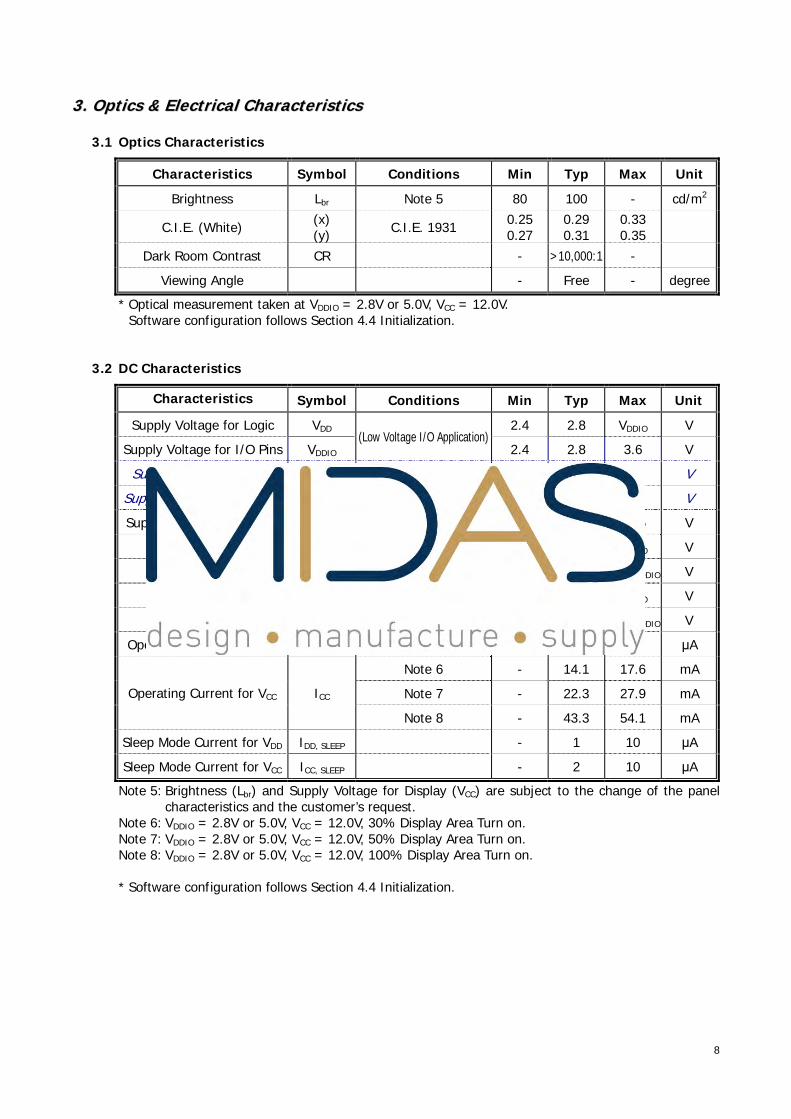
33.. OOppttiiccss && EElleeccttrriiccaall CChhaarraacctteerriissttiiccss
3.1 Optics Characteristics
Characteristics Symbol Conditions Min Typ Max Unit
Brightness Lbr Note 5 80 100 - cd/m2
C.I.E. (White) (x) (y) C.I.E. 1931 0.25
0.27 0.29 0.31
0.33 0.35
Dark Room Contrast CR - >10,000:1 -
Viewing Angle - Free - degree
* Optical measurement taken at VDDIO = 2.8V or 5.0V, VCC = 12.0V. Software configuration follows Section 4.4 Initialization.
3.2 DC Characteristics
Characteristics Symbol Conditions Min Typ Max Unit
Supply Voltage for Logic VDD 2.4 2.8 VDDIO V
Supply Voltage for I/O Pins VDDIO (Low Voltage I/O Application)
2.4 2.8 3.6 V
Supply Voltage for Logic VDD - - - V
Supply Voltage for I/O Pins VDDIO (5V I/O Application)
4.4 5.0 5.5 V
Supply Voltage for Display VCC Note 5 11.5 12.0 12.5 V
High Level Input VIH IOUT = 100μA, 3.3MHz 0.8×VDDIO - VDDIO V
Low Level Input VIL IOUT = 100μA, 3.3MHz 0 - 0.2×VDDIO V
High Level Output VOH IOUT = 100μA, 3.3MHz 0.9×VDDIO - VDDIO V
Low Level Output VOL IOUT = 100μA, 3.3MHz 0 - 0.1×VDDIO V
Operating Current for VDD IDD - 180 300 μA
Note 6 - 14.1 17.6 mA
Note 7 - 22.3 27.9 mA Operating Current for VCC ICC
Note 8 - 43.3 54.1 mA
Sleep Mode Current for VDD IDD, SLEEP - 1 10 μA
Sleep Mode Current for VCC ICC, SLEEP - 2 10 μA
Note 5: Brightness (Lbr) and Supply Voltage for Display (VCC) are subject to the change of the panel characteristics and the customer’s request.
Note 6: VDDIO = 2.8V or 5.0V, VCC = 12.0V, 30% Display Area Turn on. Note 7: VDDIO = 2.8V or 5.0V, VCC = 12.0V, 50% Display Area Turn on. Note 8: VDDIO = 2.8V or 5.0V, VCC = 12.0V, 100% Display Area Turn on. * Software configuration follows Section 4.4 Initialization.
9
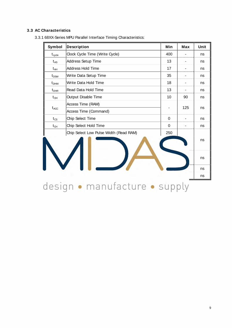
3.3 AC Characteristics
3.3.1 68XX-Series MPU Parallel Interface Timing Characteristics:
Symbol Description Min Max Unit
tcycle Clock Cycle Time (Write Cycle) 400 - ns
tAS Address Setup Time 13 - ns
tAH Address Hold Time 17 - ns
tDSW Write Data Setup Time 35 - ns
tDHW Write Data Hold Time 18 - ns
tDHR Read Data Hold Time 13 - ns
tOH Output Disable Time 10 90 ns
Access Time (RAM) tACC
Access Time (Command) - 125 ns
tCS Chip Select Time 0 - ns
tCH Chip Select Hold Time 0 - ns
Chip Select Low Pulse Width (Read RAM) 250
Chip Select Low Pulse Width (Read Command) 250 PWCSL
Chip Select Low Pulse width (Write) 50
- ns
Chip Select High Pulse Width (Read) 155 PWCSH
Chip Select High Pulse Width (Write) 55 - ns
tR Rise Time - 15 ns
tF Fall Time - 15 ns
* (VDDIO - VSS = 2.4V to 3.6V / 4.4V to 5.5V, Ta = 25°C)

10
( CS# “Low Pulse Width” > E “High Pulse Width” )
( CS# “Low Pulse Width” < E “High Pulse Width” )
D/C#
R/W#
CS#
E
D[7:0] (Write)
D[7:0] (Read)
tAS
tCS
tFtR
PWCSH PWCSL
tcycle
tDSW tDHW
tACC
Valid Data
tOH
tAH
tCH
tDHR
Valid Data
D/C#
R/W#
CS#
E
D[7:0] (Write)
D[7:0] (Read)
tFtR
tAS tAH
tCS tCH
PWCSH PWCSL
tcycle
tDSW tDHW
tACC tDHR
Valid Data
tOH
Valid Data

11
3.3.2 80XX-Series MPU Parallel Interface Timing Characteristics:
Symbol Description Min Max Unit
tcycle Clock Cycle Time (Write Cycle) 400 - ns
tAS Address Setup Time 13 - ns
tAH Address Hold Time 17 - ns
tDSW Write Data Setup Time 35 - ns
tDHW Write Data Hold Time 18 - ns
tDHR Read Data Hold Time 13 - ns
tOH Output Disable Time 10 70 ns
Access Time (RAM) tACC
Access Time (Command) - 125 ns
tCS Chip Select Time 0 - ns
tCSH Chip Select Hold Time to Read Signal 0 - ns
tCSF Chip Select Hold Time 0 - ns
Chip Select Low Pulse Width (Read RAM) - tPWLR 250
Chip Select Low Pulse Width (Read Command) - tPWLR 250 PWCSL
Chip Select Low Pulse width (Write) - tPWLW 50
- ns
Chip Select High Pulse Width (Read) - tPWHR 155 PWCSH
Chip Select High Pulse Width (Write) - tPWHW 55 - ns
tR Rise Time - 15 ns
tF Fall Time - 15 ns
* (VDDIO - VSS = 2.4V to 3.6V / 4.4V to 5.5V, Ta = 25°C)
( Read Timing )
( Write Timing )

12
3.3.3 Serial Interface Timing Characteristics:
Symbol Description Min Max Unit
tcycle Serial Clock Cycle Time 1 20 ns
tsu1 Chip Select Setup Time 60 - ns
th1 Chip Select Hold Time 20 - ns
tsu2 Serial Input Data Setup Time 200 - ns
th2 Serial Input Data Hold Time TBD - ns
tD Serial Output Data Delay Time - TBD ns
tDH Serial Output Data Hold Time 10 - ns
tW Serial Clock Width (Low, High) 400 - ns
tR Serial Clock Rise Time - 15 ns
tF Serial Clock Fall Time - 15 ns
* (VDDIO - VSS = 2.4V to 3.6V / 4.4V to 5.5V, Ta = 25°C)
SOD
CS#
SCLK
SID
VOL1
tDH
tcycle
tsu2 th2
tD
VOH1
VIL1
th1 tW
VIL1
tF
VIL1
VIH1
tsu1 tR tW
VIL1
VIH1
VIL1
VIH1
VIL1 VIH1

13
3.3.4 I2C Interface Timing Characteristics:
Symbol Description Min Max Unit
tcycle Clock Cycle Time 2.5 - μs
tHSTART Start Condition Hold Time 0.6 - μs
Data Hold Time (for “SDAOUT” Pin) 5 tHD
Data Hold Time (for “SDAIN” Pin) 300 - ns
tSD Data Setup Time 100 - ns
tSSTART Start Condition Setup Time (Only relevant for a repeated Start condition) 0.6 - μs
tSSTOP Stop Condition Setup Time 0.6 - μs
tR Rise Time for Data and Clock Pin 300 ns
tF Fall Time for Data and Clock Pin 300 ns
tIDLE Idle Time before a New Transmission can Start 1.3 - μs
* (VDDIO - VSS = 2.4V to 3.6V / 4.4V to 5.5V, Ta = 25°C)
// //
SDA
SCL
tHSTART
tCYCLE
tHD
tR
tF
tSD tSSTART tSSTOP
tIDLE

14
44.. FFuunnccttiioonnaall SSppeecciiffiiccaattiioonn
4.1 Commands
Refer to the Technical Manual for the SSD1311
4.2 Power down and Power up Sequence
To protect OEL panel and extend the panel life time, the driver IC power up/down routine should include a delay period between high voltage and low voltage power sources during turn on/off. It gives the OEL panel enough time to complete the action of charge and discharge before/after the operation.
4.2.1 Power up Sequence:
1. Power up VDD & VDDIO 2. Send Display off command 3. Initialization 4. Clear Screen 5. Power up VCC 6. Delay 100ms
(When VCC is stable) 7. Send Display on command
4.2.2 Power down Sequence:
1. Send Display off command 2. Power down VCC 3. Delay 100ms
(When VCC is reach 0 and panel is completely discharges)
4. Power down VDD & VDDIO
Note 9: 1) Since an ESD protection circuit is connected between VDD, VDDIO and VCC inside the driver IC,
VCC becomes lower than VDD & VDDIO whenever VDD & VDDIO is ON and VCC is OFF. 2) VCC should be kept float (disable) when it is OFF. 3) Power Pins (VDD, VDDIO, VCC) can never be pulled to ground under any circumstance. 4) VDD & VDDIO should not be power down before VCC power down.
4.3 Reset Circuit
When RES# input is low, the chip is initialized with the following status: 1. Display is OFF 2. 5×8 Character Mode 3. Display start position is set at display RAM address 0 4. CGRAM address counter is set at 0 5. Cursor is OFF 6. Blink is OFF 7. Contrast control register is set at 7Fh 8. OLED command set is disabled
DDiissppllaayy oonn
VDD, VDDIO
VVDDDD,, VVDDDDIIOO oonn
VVCCCC oonn
VSS/Ground
VCC
VVDDDD,, VVDDDDIIOO ooffff
VDD, VDDIO
DDiissppllaayy ooffff
VVCCCC ooffff
VSS/Ground
VCC
15
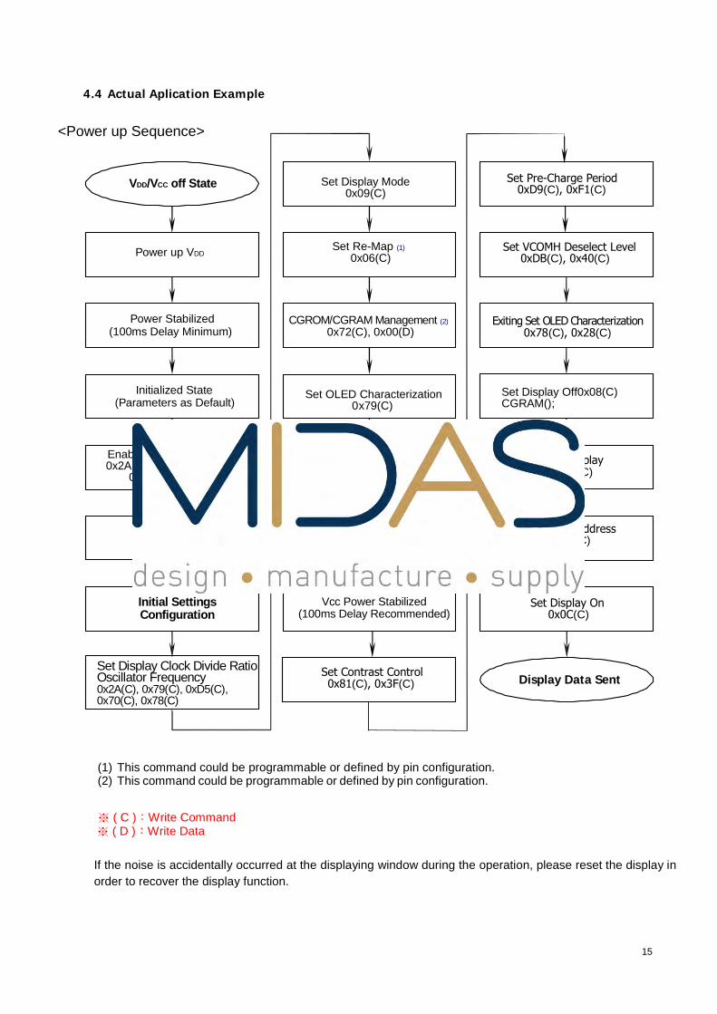
4.4 Actual Aplication Example
Set Display Mode 0x09
Set Re-Map (1) 0x06
CGROM/CGRAM Management (2)
0x72, TBD
Clear Display 0x01
Exiting Set OLED Characterization0x78, 0x28
Set DDRAM Address 0x80
Power up VDD/VDDIO (RES# as Low State)
VDD/VDDIO/VCC off State
<Power up Sequence>
(1) This command could be programmable or defined by pin configuration. (2) This command could be programmable or defined by pin configuration. ※ ( C ):Write Command
※ ( D ):Write Data
If the noise is accidentally occurred at the displaying window during the operation, please reset the display in order to recover the display function.
Set Segment Low Voltage & GPIO0xDC(C), 0x03(C)
Set Contrast Control0x81(C), 0x3F(C)
VDD/VCC off State
Power up VDD
Power Stabilized(100ms Delay Minimum)
Initialized State(Parameters as Default)
Enable Internal Regulator0x2A(C),0x08(C),0x71(C),
0x5C(D),0x28(C)
Set Display Off0x08(C)
Initial SettingsConfiguration
Set Display Mode0x09(C)
CGROM/CGRAM Management (2)0x72(C), 0x00(D)
Set OLED Characterization 0x79(C)
Set SEG Pins Hardware Configuration0xDA(C), 0x10(C)
Set Re-Map (1)0x06(C)
Set Pre-Charge Period 0xD9(C), 0xF1(C)
Set VCOMH Deselect Level 0xDB(C), 0x40(C)
Exiting Set OLED Characterization 0x78(C), 0x28(C)
Clear Display 0x01(C)
Set DDRAM Address 0x80(C)
Vcc Power Stabilized(100ms Delay Recommended)
Set Display On 0x0C(C)
Display Data SentSet Display Clock Divide Ratio Oscillator Frequency0x2A(C), 0x79(C), 0xD5(C),0x70(C), 0x78(C)
Set Display Off0x08(C)CGRAM();

<Power down Sequence>
<Entering Sleep Mode>
<Exiting Sleep Mode>
Normal Operation
Disable Internal Regulator0x2A(C), 0x71(C) 0x00(D), 0x28(C)
Sleep Mode
Power down VCC (GPIO)B
0x2A(C), 0x79(C), 0xDC(C) , 0X02(C)
Set Display Off0x78(C), 0x28(C), 0x08(C)
Sleep Mode
Disable Internal Regulator 0x2A (C),0x79 (C),0x71 (C)
0x5C (D),0xDC (C),0x03 (C)
Power up VCC
(100ms Delay Recommended)
Set Display On0x78 (C), 0x28 (C),0x0C (C)
Normal Operation

19
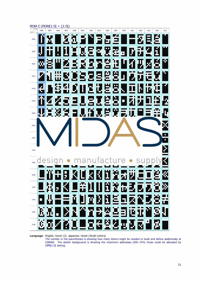
4.5 Built-in CGROM (Character Generator ROM)
ROM A (ROM[1:0] = [0:0])
Language: English, Irish, Spanish, Dutch (2), Danish, Norwegian, Swedish, Finnish, Czech (7), Slovene, Hungarian (2), Turkish
(1) The number in the parentheses is showing how many letters might be needed to build and define additionally at CGRAM. The darker background is showing the maximum addresses (00h~07h) those could be allocated by OPR[1:0] setting.

20
ROM B (ROM[1:0] = [0:1])
Language: English, Irish, Portuguese, Spanish, French (1), Italian, German, Dutch (2), Icelandic, Danish, Norwegian, Swedish,
Polish (8), Czech (8), Hungarian (2), Romanian (5), Turkish, Vietnamese (6), Russian (Small Letters) The number in the parentheses is showing how many letters might be needed to build and define additionally at CGRAM. The darker background is showing the maximum addresses (00h~07h) those could be allocated by OPR[1:0] setting.
21
ROM C (ROM[1:0] = [1:0])
Language: English, Dutch (2), Japanese, Greek (Small Letters)
The number in the parentheses is showing how many letters might be needed to build and define additionally at CGRAM. The darker background is showing the maximum addresses (00h~07h) those could be allocated by OPR[1:0] setting.

22
4.6 Self-Defined CGRAM (Character Generator RAM)
8 Addresses Available for Self-Defined Characters (OPR[1:0] = [0:0])
8 Addresses Available for Self-Defined Characters (OPR[1:0] = [0:1])
6 Addresses Available for Self-Defined Characters (OPR[1:0] = [1:0])
0 Address Available for Self-Defined Characters (OPR[1:0] = [1:1])

23
55.. RReelliiaabbiilliittyy
5.1 Contents of Reliability Tests
Item Conditions Criteria
High Temperature Operation 85°C, 240 hrs
Low Temperature Operation -40°C, 240 hrs
High Temperature Storage 90°C, 240 hrs
Low Temperature Storage -40°C, 240 hrs
High Temperature/Humidity Operation 60°C, 90% RH, 240 hrs
Thermal Shock -40°C ⇔ 85°C, 100 cycles 60 mins dwell
The operational functions work.
* The samples used for the above tests do not include polarizer. * No moisture condensation is observed during tests.
5.2 Failure Check Standard
After the completion of the described reliability test, the samples were left at room temperature for 2 hrs prior to conducting the failure test at 23±5°C; 55±15% RH.
24
66.. OOuuttggooiinngg QQuuaalliittyy CCoonnttrrooll SSppeecciiffiiccaattiioonnss
6.1 Environment Required
Customer’s test & measurement are required to be conducted under the following conditions: Temperature: 23 ± 5°C Humidity: 55 ± 15% RH Fluorescent Lamp: 30W Distance between the Panel & Lamp: ≥ 50cm Distance between the Panel & Eyes of the Inspector: ≥ 30cm Finger glove (or finger cover) must be worn by the inspector. Inspection table or jig must be anti-electrostatic.
6.2 Sampling Plan
Level II, Normal Inspection, Single Sampling, MIL-STD-105E
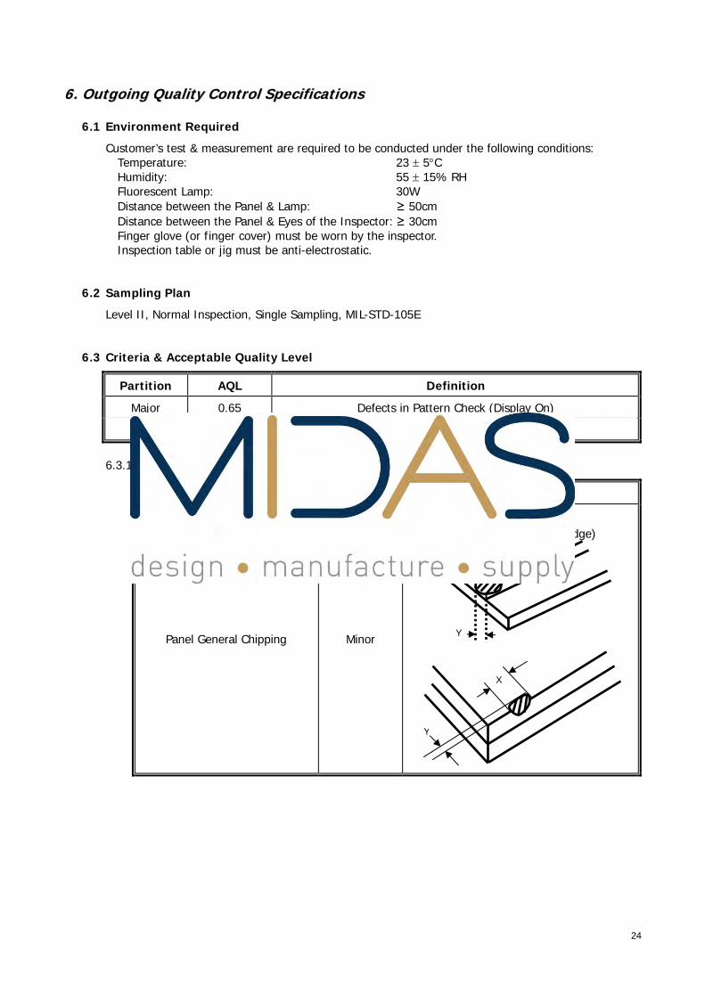
6.3 Criteria & Acceptable Quality Level
Partition AQL Definition
Major 0.65 Defects in Pattern Check (Display On)
Minor 1.0 Defects in Cosmetic Check (Display Off)
6.3.1 Cosmetic Check (Display Off) in Non-Active Area
Check Item Classification Criteria
Panel General Chipping Minor
X > 6 mm (Along with Edge) Y > 1 mm (Perpendicular to edge)
X
Y
X
Y

25
6.3.1 Cosmetic Check (Display Off) in Non-Active Area (Continued)
Check Item Classification Criteria
Panel Crack Minor
Any crack is not allowable.
Copper Exposed
(Even Pin or Film) Minor Not Allowable by Naked Eye Inspection
Film or Trace Damage Minor
Terminal Lead Prober Mark Acceptable
Glue or Contamination on Pin (Couldn’t Be Removed by Alcohol) Minor
Ink Marking on Back Side of panel(Exclude on Film) Acceptable Ignore for Any
26
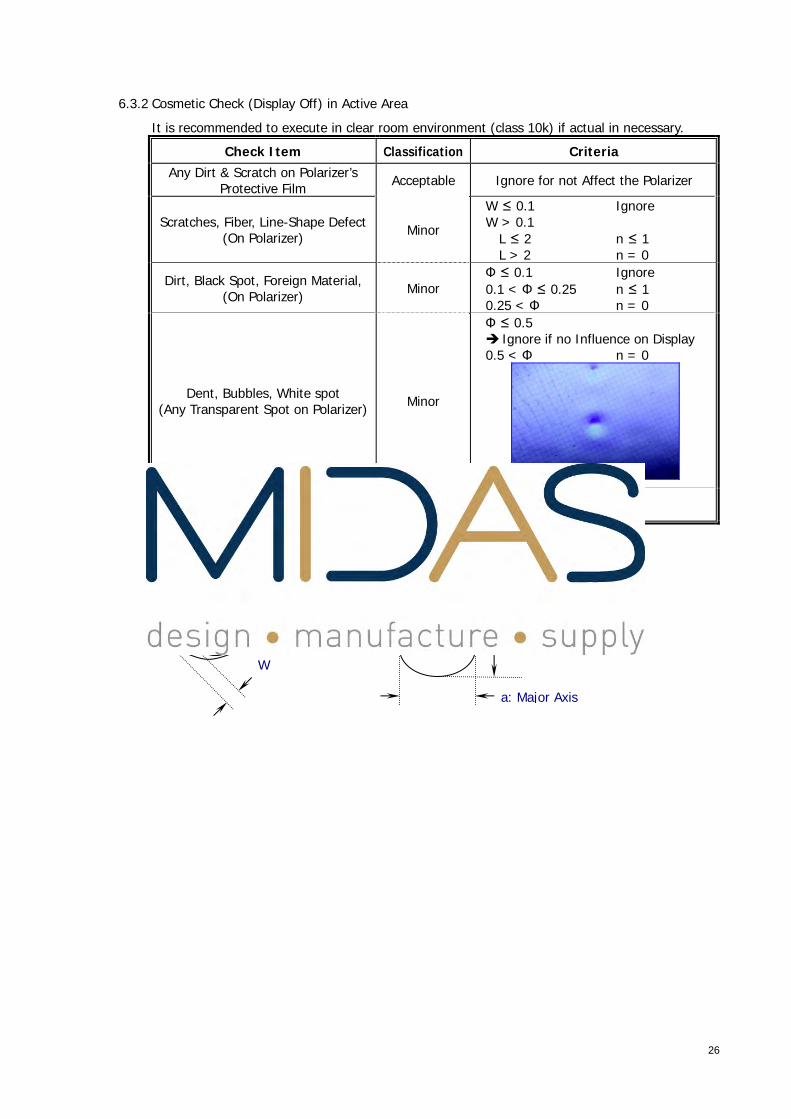
6.3.2 Cosmetic Check (Display Off) in Active Area
It is recommended to execute in clear room environment (class 10k) if actual in necessary.
Check Item Classification Criteria Any Dirt & Scratch on Polarizer’s
Protective Film Acceptable Ignore for not Affect the Polarizer
Scratches, Fiber, Line-Shape Defect(On Polarizer) Minor
W ≤ 0.1 Ignore W > 0.1
L ≤ 2 n ≤ 1 L > 2 n = 0
Dirt, Black Spot, Foreign Material, (On Polarizer) Minor
Φ ≤ 0.1 Ignore 0.1 < Φ ≤ 0.25 n ≤ 1 0.25 < Φ n = 0
Dent, Bubbles, White spot (Any Transparent Spot on Polarizer) Minor
Φ ≤ 0.5 Ignore if no Influence on Display
0.5 < Φ n = 0
Fingerprint, Flow Mark (On Polarizer) Minor Not Allowable
* Protective film should not be tear off when cosmetic check. ** Definition of W & L & Φ (Unit: mm): Φ = (a + b) / 2
W
L
b: Minor Axis
a: Major Axis
27
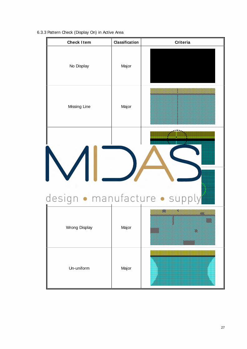
6.3.3 Pattern Check (Display On) in Active Area
Check Item Classification Criteria
No Display Major
Missing Line Major
Pixel Short Major
Darker Pixel Major
Wrong Display Major
Un-uniform Major

28
77.. PPaacckkaaggee SSppeecciiffiiccaattiioonnss
B pcs Tray with Vacuum Packing
Primary Box (L450mm x W296mm x H110mm, B wave)x C Set
Module
Tray (420mm x 285mm)
Carton Box
Carton Box(Major / Maximum: L464mm x W313mm x H472mm, AB wave)
C Set Primary Box
Label
Vacuum Packing Bag
Sponge Protective(370mm x 280mm x 20mm)
Staggered Stacking
Sponge Protective
x 1 pcs (Empty)
x A pcs
Wrapped with Adhesive Tapex B pcs
Item Quantity
Module 320 per Primary Box
Holding Trays (A) 20 per Primary Box
Total Trays (B) 21 per Primary Box (Including 1 Empty Tray)
Primary Box (C) 1~4 per Carton (4 as Major / Maximum)

29
88.. PPrreeccaauuttiioonnss WWhheenn UUssiinngg TThheessee OOEELL DDiissppllaayy MMoodduulleess
8.1 Handling Precautions
1) Since the display panel is being made of glass, do not apply mechanical impacts such us dropping from a high position.
2) If the display panel is broken by some accident and the internal organic substance leaks out, be careful not to inhale nor lick the organic substance.
3) If pressure is applied to the display surface or its neighborhood of the OEL display module, the cell structure may be damaged and be careful not to apply pressure to these sections.
4) The polarizer covering the surface of the OEL display module is soft and easily scratched. Please be careful when handling the OEL display module.
5) When the surface of the polarizer of the OEL display module has soil, clean the surface. It takes advantage of by using following adhesion tape. * Scotch Mending Tape No. 810 or an equivalent Never try to breathe upon the soiled surface nor wipe the surface using cloth containing solvent such as ethyl alcohol, since the surface of the polarizer will become cloudy. Also, pay attention that the following liquid and solvent may spoil the polarizer: * Water * Ketone * Aromatic Solvents
6) Hold OEL display module very carefully when placing OEL display module into the system housing. Do not apply excessive stress or pressure to OEL display module. And, do not over bend the film with electrode pattern layouts. These stresses will influence the display performance. Also, secure sufficient rigidity for the outer cases.
7) Do not apply stress to the driver IC and the surrounding molded sections. 8) Do not disassemble nor modify the OEL display module. 9) Do not apply input signals while the logic power is off. 10) Pay sufficient attention to the working environments when handing OEL display modules to prevent
occurrence of element breakage accidents by static electricity. * Be sure to make human body grounding when handling OEL display modules. * Be sure to ground tools to use or assembly such as soldering irons. * To suppress generation of static electricity, avoid carrying out assembly work under dry
environments. * Protective film is being applied to the surface of the display panel of the OEL display module.
Be careful since static electricity may be generated when exfoliating the protective film. 11) Protection film is being applied to the surface of the display panel and removes the protection film
before assembling it. At this time, if the OEL display module has been stored for a long period of time, residue adhesive material of the protection film may remain on the surface of the display panel after removed of the film. In such case, remove the residue material by the method introduced in the above Section 5).
12) If electric current is applied when the OEL display module is being dewed or when it is placed under high humidity environments, the electrodes may be corroded and be careful to avoid the above.
8.2 Storage Precautions
1) When storing OEL display modules, put them in static electricity preventive bags avoiding exposure to direct sun light nor to lights of fluorescent lamps. and, also, avoiding high temperature and high

30
humidity environment or low temperature (less than 0°C) environments. (We recommend you to store these modules in the packaged state when they were shipped from Midas Displays) At that time, be careful not to let water drops adhere to the packages or bags nor let dewing occur with them.
2) If electric current is applied when water drops are adhering to the surface of the OEL display module, when the OEL display module is being dewed or when it is placed under high humidity environments, the electrodes may be corroded and be careful about the above.
8.3 Designing Precautions
1) The absolute maximum ratings are the ratings which cannot be exceeded for OEL display module, and if these values are exceeded, panel damage may be happen.
2) To prevent occurrence of malfunctioning by noise, pay attention to satisfy the VIL and VIH specifications and, at the same time, to make the signal line cable as short as possible.
3) We recommend you to install excess current preventive unit (fuses, etc.) to the power circuit (VDD). (Recommend value: 0.5A)
4) Pay sufficient attention to avoid occurrence of mutual noise interference with the neighboring devices.
5) As for EMI, take necessary measures on the equipment side basically. 6) When fastening the OEL display module, fasten the external plastic housing section. 7) If power supply to the OEL display module is forcibly shut down by such errors as taking out the
main battery while the OEL display panel is in operation, we cannot guarantee the quality of this OEL display module.
8) The electric potential to be connected to the rear face of the IC chip should be as follows: SSD1311 * Connection (contact) to any other potential than the above may lead to rupture of the IC.
8.4 Precautions when disposing of the OEL display modules
1) Request the qualified companies to handle industrial wastes when disposing of the OEL display modules. Or, when burning them, be sure to observe the environmental and hygienic laws and regulations.
8.5 Other Precautions
1) When an OEL display module is operated for a long of time with fixed pattern may remain as an after image or slight contrast deviation may occur. Nonetheless, if the operation is interrupted and left unused for a while, normal state can be restored. Also, there will be no problem in the reliability of the module.
2) To protect OEL display modules from performance drops by static electricity rapture, etc., do not touch the following sections whenever possible while handling the OEL display modules. * Pins and electrodes * Pattern layouts such as the FPC
3) With this OEL display module, the OEL driver is being exposed. Generally speaking, semiconductor elements change their characteristics when light is radiated according to the principle of the solar battery. Consequently, if this OEL driver is exposed to light, malfunctioning may occur. * Design the product and installation method so that the OEL driver may be shielded from light in
actual usage. * Design the product and installation method so that the OEL driver may be shielded from light
during the inspection processes. 4) Although this OEL display module stores the operation state data by the commands and the
indication data, when excessive external noise, etc. enters into the module, the internal status may be changed. It therefore is necessary to take appropriate measures to suppress noise generation or to protect from influences of noise on the system design.
5) We recommend you to construct its software to make periodical refreshment of the operation

31
statuses (re-setting of the commands and re-transference of the display data) to cope with catastrophic noise.
WWaarrrraannttyy:: The warranty period shall last twelve (12) months from the date of delivery. Buyer shall be completed to assemble all the processes within the effective twelve (12) months. Midas Displays shall be liable for replacing any products which contain defective material or process which do not conform to the product specification, applicable drawings and specifications during the warranty period. All products must be preserved, handled and appearance to permit efficient handling during warranty period. The warranty coverage would be exclusive while the returned goods are out of the terms above. NNoottiiccee::
No part of this material may be reproduces or duplicated in any form or by any means without the written permission of Midas Displays. Midas Displays reserves the right to make changes to this material without notice. Midas Displays does not assume any liability of any kind arising out of any inaccuracies contained in this material or due to its application or use in any product or circuit and, further, there is no representation that this material is applicable to products requiring high level reliability, such as, medical products. Moreover, no license to any intellectual property rights is granted by implication or otherwise, and there is no representation or warranty that anything made in accordance with this material will be free from any patent or copyright infringement of a third party. This material or portions thereof may contain technology or the subject relating to strategic products under the control of Foreign Exchange and Foreign Trade Law of Taiwan and may require an export license from the Ministry of International Trade and Industry or other approval from another government agency.