PART NUMBER: ± 2g Tri-axis Digital Accelerometer ...akizukidenshi.com/download/ds/kionix/KXSD9-2050...
25
± 2g Tri-axis Digital Accelerometer Specifications PART NUMBER: KXSD9-2050 Rev. 3 Jul-2010 36 Thornwood Dr. – Ithaca, NY 14850 © 2009 Kionix – All Rights Reserved tel: 607-257-1080 – fax:607-257-1146 310-1547-1007221647 www.kionix.com - [email protected] Page 1 of 25 Product Description The KXSD9 is a tri-axis silicon micromachined accelerometer with a user selectable full-scale output range of ±2g, ±4g, ±6g or ±8g. The sense element is fabricated using Kionix’s proprietary plasma micromachining process technology. Acceleration sensing is based on the principle of a differential capacitance arising from acceleration-induced motion of the sense element, which further utilizes common mode cancellation to decrease errors from process variation, temperature, and environmental stress. The sense element is hermetically sealed at the wafer level by bonding a second silicon lid wafer to the device using a glass frit. A separate ASIC device packaged with the sense element provides signal conditioning, self-test, and temperature compensation. The accelerometer is delivered in a 3 x 3 x 0.9 mm LGA plastic package operating from a 1.8 – 3.6V DC supply. Either I 2 C or SPI interfaces can be used to communicate to the chip to trigger A/D conversions or manage power consumption. Functional Diagram X Sensor Vdd IO Vdd GND Y Sensor Z Sensor 8 6 10 SPI/I 2 C Motion Detection Charge Amp A/D 5 1 4 Temp Sensor LPF 9 AUX IN 3 7
Transcript of PART NUMBER: ± 2g Tri-axis Digital Accelerometer ...akizukidenshi.com/download/ds/kionix/KXSD9-2050...

± 2g Tri-axis Digital Accelerometer
Specifications
PART NUMBER:
KXSD9-2050 Rev. 3
Jul-2010
36 Thornwood Dr. – Ithaca, NY 14850 © 2009 Kionix – All Rights Reserved tel: 607-257-1080 – fax:607-257-1146 310-1547-1007221647 www.kionix.com - [email protected] Page 1 of 25
Product Description
The KXSD9 is a tri-axis silicon micromachined accelerometer with a user selectable full-scale output range of ±2g, ±4g, ±6g or ±8g. The sense element is fabricated using Kionix’s proprietary plasma micromachining process technology. Acceleration sensing is based on the principle of a differential capacitance arising from acceleration-induced motion of the sense element, which further utilizes common mode cancellation to decrease errors from process variation, temperature, and environmental stress. The sense element is hermetically sealed at the wafer level by bonding a second silicon lid wafer to the device using a glass frit. A separate ASIC device packaged with the sense element provides signal conditioning, self-test, and temperature compensation. The accelerometer is delivered in a 3 x 3 x 0.9 mm LGA plastic package operating from a 1.8 – 3.6V DC supply. Either I2C or SPI interfaces can be used to communicate to the chip to trigger A/D conversions or manage power consumption.
Functional Diagram
X Sensor
Vdd
IO Vdd
GND
Y Sensor
Z Sensor
86 10
SPI/I 2CMotion Detection
Charge Amp
A/D5
1
4
TempSensor
LPF
9
AUX IN3
7
参考資料カラー
± 2g Tri-axis Digital Accelerometer
Specifications
PART NUMBER:
KXSD9-2050 Rev. 3
Jul-2010
36 Thornwood Dr. – Ithaca, NY 14850 © 2009 Kionix – All Rights Reserved tel: 607-257-1080 – fax:607-257-1146 310-1547-1007221647 www.kionix.com - [email protected] Page 2 of 25
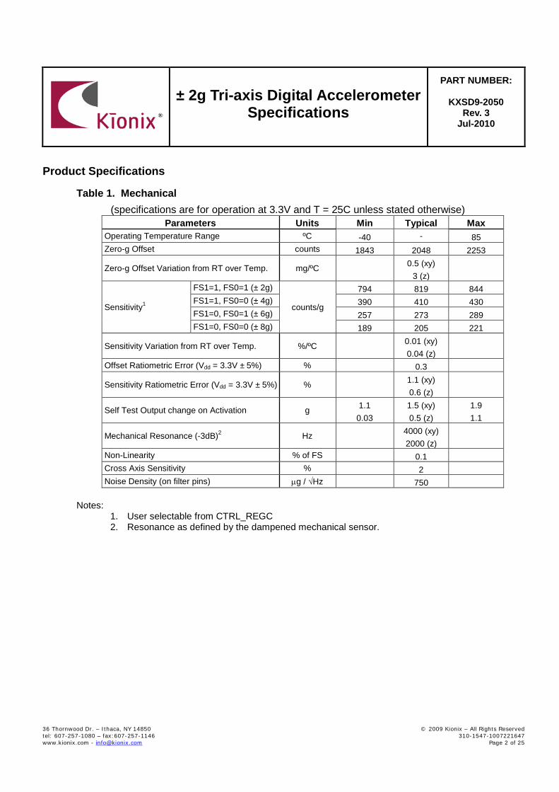
Product Specifications Table 1. Mechanical
(specifications are for operation at 3.3V and T = 25C unless stated otherwise) Parameters Units Min Typical Max
Operating Temperature Range ºC -40 - 85 Zero-g Offset counts 1843 2048 2253
Zero-g Offset Variation from RT over Temp. mg/ºC
0.5 (xy) 3 (z)
Sensitivity1
FS1=1, FS0=1 (± 2g)
counts/g
794 819 844 FS1=1, FS0=0 (± 4g) 390 410 430 FS1=0, FS0=1 (± 6g) 257 273 289 FS1=0, FS0=0 (± 8g) 189 205 221
Sensitivity Variation from RT over Temp. %/ºC
0.01 (xy) 0.04 (z)
Offset Ratiometric Error (Vdd = 3.3V ± 5%) % 0.3
Sensitivity Ratiometric Error (Vdd = 3.3V ± 5%) %
1.1 (xy) 0.6 (z)
Self Test Output change on Activation g 1.1 0.03
1.5 (xy) 0.5 (z)
1.9 1.1
Mechanical Resonance (-3dB)2 Hz
4000 (xy) 2000 (z)
Non-Linearity % of FS 0.1 Cross Axis Sensitivity % 2 Noise Density (on filter pins) µg / √Hz 750
Notes:
1. User selectable from CTRL_REGC 2. Resonance as defined by the dampened mechanical sensor.

± 2g Tri-axis Digital Accelerometer
Specifications
PART NUMBER:
KXSD9-2050 Rev. 3
Jul-2010
36 Thornwood Dr. – Ithaca, NY 14850 © 2009 Kionix – All Rights Reserved tel: 607-257-1080 – fax:607-257-1146 310-1547-1007221647 www.kionix.com - [email protected] Page 3 of 25
Table 2. Electrical
(specifications are for operation at 3.3V and T = 25C unless stated otherwise)
Parameters Units Min Typical Max Supply Voltage (Vdd) Operating V 1.8 3.3 3.6 I/O Pads Supply Voltage (VIO) V 1.7 Vdd
Current Consumption
Operating (full power)
µA
120 220 320 Motion Wake Up 15Hz Mode 40 75
Standby 0.1 Output Low Voltage1 V - - 0.3 * Vio Output High Voltage V 0.9 * Vio - - Input Low Voltage V - - 0.2 * Vio Input High Voltage V 0.8 * Vio - - Input Pull-down Current µA 0
Power Up Time2
LPF (-3dB) = 50Hz
ms
15.9 LPF (-3dB) = 100Hz 8.0 LPF (-3dB) = 500Hz 1.6 LPF (-3dB) = 1,000Hz 0.8 LPF (-3dB) = 2,000Hz 0.4
A/D Conversion time µs 200 SPI Communication Rate3 MHz 1 I2C Communication Rate KHz 400 Bandwidth (-3dB)4 Hz 40 50 60
Notes:
1. Assuming I2C communication and minimum 1.5Kohm pull-up resistor on SCL and
SDA. 2. Power up time is determined after the enabling of the part and is determined by the
low-pass filter (LPF) set in CTRL_REGC. 3. SPI Communication Rate can be optimized for faster communication per the SPI
timing diagram below. 4. Factory programmable to have a switched capacitor low pass filter at 2kHz, 1kHz,
500Hz, 100Hz, 50Hz or no low pass filter. Optionally, the user can define with in CTRL_REGC. Maximum defined by the frequency response of the sensors.
± 2g Tri-axis Digital Accelerometer
Specifications
PART NUMBER:
KXSD9-2050 Rev. 3
Jul-2010
36 Thornwood Dr. – Ithaca, NY 14850 © 2009 Kionix – All Rights Reserved tel: 607-257-1080 – fax:607-257-1146 310-1547-1007221647 www.kionix.com - [email protected] Page 4 of 25
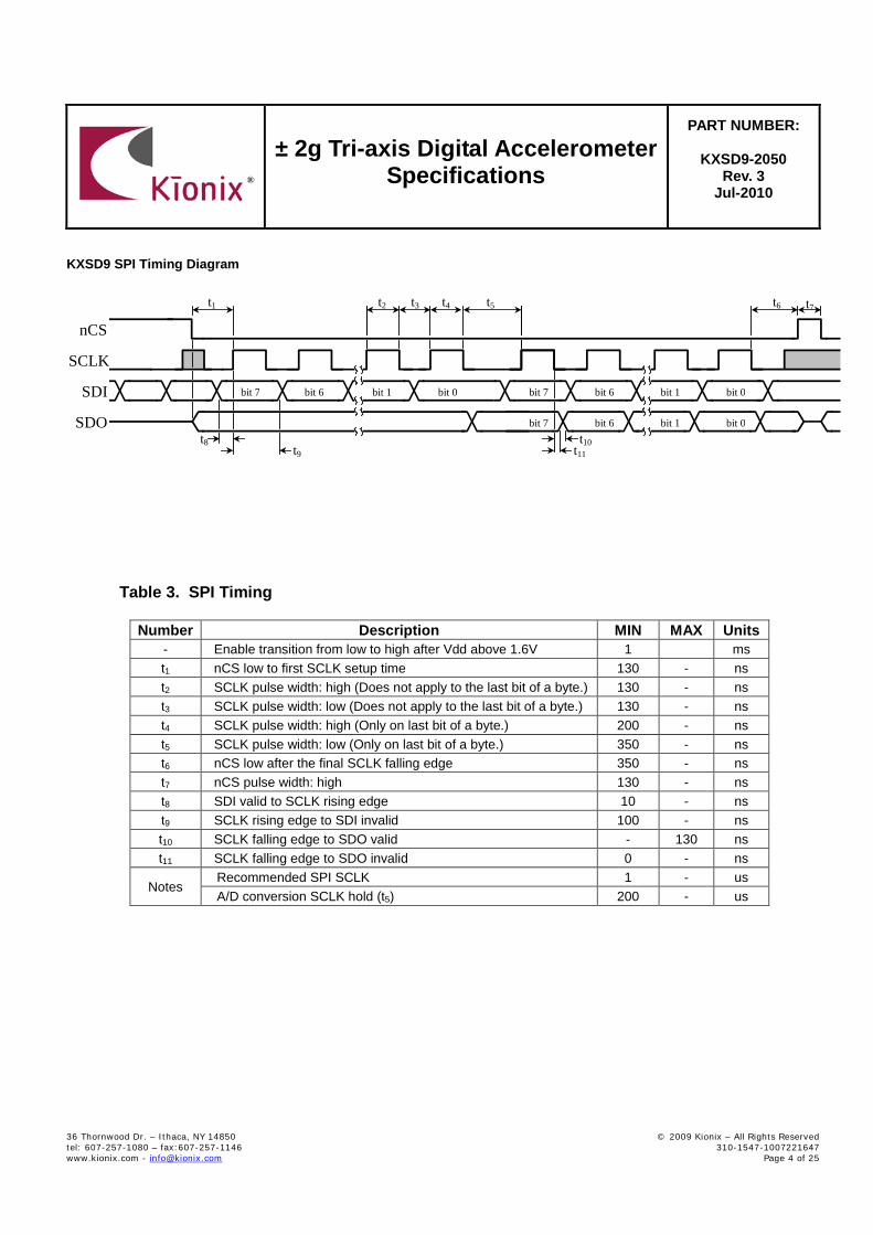
KXSD9 SPI Timing Diagram
SDO
SDI
nCS
t1
SCLK
bit 7 bit 6 bit 1
bit 0 bit 7
bit 6 bit 1
bit 0
bit 7
bit 6 bit 1
bit 0
t2 t3 t4 t5 t6 t7
t8 t9
t10 t11
Table 3. SPI Timing
Number Description MIN MAX Units - Enable transition from low to high after Vdd above 1.6V 1 ms t1 nCS low to first SCLK setup time 130 - ns t2 SCLK pulse width: high (Does not apply to the last bit of a byte.) 130 - ns t3 SCLK pulse width: low (Does not apply to the last bit of a byte.) 130 - ns t4 SCLK pulse width: high (Only on last bit of a byte.) 200 - ns t5 SCLK pulse width: low (Only on last bit of a byte.) 350 - ns t6 nCS low after the final SCLK falling edge 350 - ns t7 nCS pulse width: high 130 - ns t8 SDI valid to SCLK rising edge 10 - ns t9 SCLK rising edge to SDI invalid 100 - ns t10 SCLK falling edge to SDO valid - 130 ns t11 SCLK falling edge to SDO invalid 0 - ns
Notes Recommended SPI SCLK 1 - us A/D conversion SCLK hold (t5) 200 - us

± 2g Tri-axis Digital Accelerometer
Specifications
PART NUMBER:
KXSD9-2050 Rev. 3
Jul-2010
36 Thornwood Dr. – Ithaca, NY 14850 © 2009 Kionix – All Rights Reserved tel: 607-257-1080 – fax:607-257-1146 310-1547-1007221647 www.kionix.com - [email protected] Page 5 of 25
HF
Table 4. Environmental
Parameters Units Min Typical Max Supply Voltage (Vdd) Absolute Limits V -0.3 - 6.0 Operating Temperature Range ºC -40 - 85 Storage Temperature Range ºC -55 - 150
Mech. Shock (powered and unpowered) g - - 5000 for 0.5ms 10000 for 0.2ms
ESD HBM V - - 2000
Caution: ESD Sensitive and Mechanical Shock Sensitive Component, improper handling can cause permanent damage to the device.
This product conforms to Directive 2002/95/EC of the European Parliament and of the Council of the European Union (RoHS). Specifically, this product does not contain lead, mercury, cadmium, hexavalent chromium, polybrominated biphenyls (PBB), or polybrominated diphenyl ethers (PBDE) above the maximum concentration values (MCV) by weight in any of its homogenous materials. Homogenous materials are "of
uniform composition throughout."
This product is halogen-free per IEC 61249-2-21. Specifically, the materials used in this product contain a maximum total halogen content of 1500 ppm with less than 900-ppm bromine and less than 900-ppm chlorine.
Soldering
Soldering recommendations are available upon request or from www.kionix.com.

± 2g Tri-axis Digital Accelerometer
Specifications
PART NUMBER:
KXSD9-2050 Rev. 3
Jul-2010
36 Thornwood Dr. – Ithaca, NY 14850 © 2009 Kionix – All Rights Reserved tel: 607-257-1080 – fax:607-257-1146 310-1547-1007221647 www.kionix.com - [email protected] Page 6 of 25
Application Schematic
1
2
3
45
6
7
8
9
10
VddC1
SCL/SCLK
SDA/SDO
ADDR/SDI
KXSD9MOT
IO Vdd
AUX IN
CS
Table 5. KXSD9 Pin Descriptions
Pin Name Description 1 IO Vdd The power supply input for the digital communication bus
2 DNC Reserved – Do Not Connect
3 AUX IN Auxiliary Input for analog/digital conversion
4 GND Ground
5 Vdd The power supply input. Decouple this pin to ground with a 0.1uF ceramic capacitor.
6 nCS SPI Enable I2C/SPI mode selection (1 = I2C mode, 0 = SPI mode)
7 MOT Motion Wakeup Interrupt
8 ADDR/SDI I2C programmable address bit/SPI Serial Data Input
9 SCL/SCLK I2C Serial Clock/SPI Serial Clock
10 SDA/SD0 I2C Serial Data/SPI Serial Data Output

± 2g Tri-axis Digital Accelerometer
Specifications
PART NUMBER:
KXSD9-2050 Rev. 3
Jul-2010
36 Thornwood Dr. – Ithaca, NY 14850 © 2009 Kionix – All Rights Reserved tel: 607-257-1080 – fax:607-257-1146 310-1547-1007221647 www.kionix.com - [email protected] Page 7 of 25
Test Specifications
! Special Characteristics:
These characteristics have been identified as being critical to the customer. Every part is tested to verify its conformance to specification prior to shipment.
Table 6. Test Specifications
Parameter Specification Test Conditions Zero-g Offset @ RT 2048 +/- 205 counts 25C, Vdd = 3.3 V Sensitivity @ RT 819 +/- 25 counts/g 25C, Vdd = 3.3 V Current Consumption -- Operating 120 <= Idd <= 320 uA 25C, Vdd = 3.3 V

± 2g Tri-axis Digital Accelerometer
Specifications
PART NUMBER:
KXSD9-2050 Rev. 3
Jul-2010
36 Thornwood Dr. – Ithaca, NY 14850 © 2009 Kionix – All Rights Reserved tel: 607-257-1080 – fax:607-257-1146 310-1547-1007221647 www.kionix.com - [email protected] Page 8 of 25
Package Dimensions and Orientation
3 x 3 x 0.9 mm LGA
All dimensions and tolerances conform to ASME Y14.5M-1994

± 2g Tri-axis Digital Accelerometer
Specifications
PART NUMBER:
KXSD9-2050 Rev. 3
Jul-2010
36 Thornwood Dr. – Ithaca, NY 14850 © 2009 Kionix – All Rights Reserved tel: 607-257-1080 – fax:607-257-1146 310-1547-1007221647 www.kionix.com - [email protected] Page 9 of 25
Orientation
When device is accelerated in +X, +Y or +Z direction, the corresponding output will increase.
FS1=1, FS0=1 (± 2g) Static X/Y/Z Output Response versus Orientation to Earth’s surface (1-g):
Position 1 2 3 4 5 6 Diagram
Top Bottom
Bottom Top
X 2048 counts
2867 counts
2048 counts
1229 counts
2048 counts
2048 counts
Y 2867 counts
2048 counts
1229 counts
2048 counts
2048 counts
2048 counts
Z 2048 counts
2048 counts
2048 counts
2048 counts
2867 counts
1229 counts
X-Polarity 0 + 0 - 0 0 Y-Polarity + 0 - 0 0 0 Z-Polarity 0 0 0 0 + -
(1-g) Earth’s Surface
Pin 1
+X
+Y
+Z

± 2g Tri-axis Digital Accelerometer
Specifications
PART NUMBER:
KXSD9-2050 Rev. 3
Jul-2010
36 Thornwood Dr. – Ithaca, NY 14850 © 2009 Kionix – All Rights Reserved tel: 607-257-1080 – fax:607-257-1146 310-1547-1007221647 www.kionix.com - [email protected] Page 10 of 25
KXSD9 Digital Interfaces The Kionix KXSD9 digital accelerometer has the ability to communicate on both I2C and SPI digital serial interface busses. This flexibility allows for easy system integration by eliminating analog-to-digital converter requirements and by providing direct communication with system micro-controllers. In doing so, all of the digital communication pins have shared responsibilities. The serial interface terms and descriptions as indicated in Table 7 below will be observed throughout this document.
Term Description Transmitter The device that transmits data to the bus. Receiver The device that receives data from the bus. Master The device that initiates a transfer, generates clock signals and terminates a transfer. Slave The device addressed by the Master.
Table 7. Serial Interface Terminologies
I2C Serial Interface The KXSD9 has the ability to communicate on an I2C bus. I2C is primarily used for synchronous serial communication between a Master device and one or more Slave devices. The Master, typically a micro controller, provides the serial clock signal and addresses Slave devices on the bus. The KXSD9 always operates as a Slave device during standard Master-Slave I2C operation as shown in Figure 1 on the following page. I2C is a two-wire serial interface that contains a Serial Clock (SCL) line and a Serial Data (SDA) line. SCL is a serial clock that is provided by the Master, but can be held low by any Slave device, putting the Master into a wait condition. SDA is a bi-directional line used to transmit and receive data to and from the interface. Data is transmitted MSB (Most Significant Bit) first in 8-bit per byte format, and the number of bytes transmitted per transfer is unlimited. The I2C bus is considered free when both lines are high.

± 2g Tri-axis Digital Accelerometer
Specifications
PART NUMBER:
KXSD9-2050 Rev. 3
Jul-2010
36 Thornwood Dr. – Ithaca, NY 14850 © 2009 Kionix – All Rights Reserved tel: 607-257-1080 – fax:607-257-1146 310-1547-1007221647 www.kionix.com - [email protected] Page 11 of 25
MCU
SDA SCL Vdd
SDA
SCL
KXSD9
ADDR
SDA
SCL
KXSD9
ADDR
SDA
SCL
Figure 1 Multiple KXSD9 I2C Connection
I2C Operation Transactions on the I2C bus begin after the Master transmits a start condition (S), which is defined as a high-to-low transition on the data line while the SCL line is held high. The bus is considered busy after this condition. The next byte of data transmitted after the start condition contains the Slave Address (SAD) in the seven MSBs (Most Significant Bits), and the LSB (Least Significant Bit) tells whether the Master will be receiving data ‘1’ from the Slave or transmitting data ‘0’ to the Slave. When a Slave Address is sent, each device on the bus compares the seven MSBs with its internally-stored address. If they match, the device considers itself addressed by the Master. The KXSD9’s Slave Address is comprised of a programmable part and a fixed part, which allows for connection of multiple KXSD9's to the same I2C bus. The Slave Address associated with the KXSD9 is 001100X, where the programmable bit, X, is determined by the assignment of ADDR (pin 8) to GND or Vdd. Figure 1 above shows how two KXSD9's would be implemented on an I2C bus. It is mandatory that receiving devices acknowledge (ACK) each transaction. Therefore, the transmitter must release the SDA line during this ACK pulse. The receiver then pulls the data line low so that it remains stable low during the high period of the ACK clock pulse. A receiver that has been addressed, whether it is Master or Slave, is obliged to generate an ACK after each byte of data has been received. To conclude a transaction, the Master must transmit a stop condition (P) by transitioning the SDA line from low to high while SCL is high. The I2C bus is now free.

± 2g Tri-axis Digital Accelerometer
Specifications
PART NUMBER:
KXSD9-2050 Rev. 3
Jul-2010
36 Thornwood Dr. – Ithaca, NY 14850 © 2009 Kionix – All Rights Reserved tel: 607-257-1080 – fax:607-257-1146 310-1547-1007221647 www.kionix.com - [email protected] Page 12 of 25
Writing to a KXSD9 8-bit Register Upon power up, the Master must write to the KXSD9’s control registers to set its operational mode. Therefore, when writing to a control register on the I2C bus, as shown Sequence 1 on the following page, the following protocol must be observed: After a start condition, SAD+W transmission, and the KXSD9 ACK has been returned, an 8-bit Register Address (RA) command is transmitted by the Master. This command is telling the KXSD9 to which 8-bit register the Master will be writing the data. Since this is I2C mode, the MSB of the RA command should always be zero (0). The KXSD9 acknowledges the RA and the Master transmits the data to be stored in the 8-bit register. The KXSD9 acknowledges that it has received the data and the Master transmits a stop condition (P) to end the data transfer. The data sent to the KXSD9 is now stored in the appropriate register. The KXSD9 automatically increments the received RA commands and, therefore, multiple bytes of data can be written to sequential registers after each Slave ACK as shown in Sequence 2 on the following page. Reading from a KXSD9 8-bit Register When reading data from a KXSD9 8-bit register on the I2C bus, as shown in Sequence 3 on the next page, the following protocol must be observed: The Master first transmits a start condition (S) and the appropriate Slave Address (SAD) with the LSB set at ‘0’ to write. The KXSD9 acknowledges and the Master transmits the 8-bit RA of the register it wants to read. The KXSD9 again acknowledges, and the Master transmits a repeated start condition (Sr). After the repeated start condition, the Master addresses the KXSD9 with a ‘1’ in the LSB (SAD+R) to read from the previously selected register. The Slave then acknowledges and transmits the data from the requested register. The Master does not acknowledge (NACK) it received the transmitted data, but transmits a stop condition to end the data transfer. Note that the KXSD9 automatically increments through its sequential registers, allowing data reads from multiple registers following a single SAD+R command as shown below in Sequence 4 on the following page. If a receiver cannot transmit or receive another complete byte of data until it has performed some other function, it can hold SCL low to force the transmitter into a wait state. Data transfer only continues when the receiver is ready for another byte and releases SCL. For instance, after the Master has requested to read acceleration data from the KXSD9, the KXSD9 can hold SCL low to force the Master into a wait state while it completes the A/D conversion. After the A/D conversion, the KXSD9 will release SCL and transmit the acceleration data to the Master. Note that the KXSD9 will hold for A/D conversions only if the CLKhld bit is set in CTRL_REGB. Data Transfer Sequences The following information clearly illustrates the variety of data transfers that can occur on the I2C bus and how the Master and Slave interact during these transfers. Table 8 on the following page defines the I2C terms used during the data transfers.

± 2g Tri-axis Digital Accelerometer
Specifications
PART NUMBER:
KXSD9-2050 Rev. 3
Jul-2010
36 Thornwood Dr. – Ithaca, NY 14850 © 2009 Kionix – All Rights Reserved tel: 607-257-1080 – fax:607-257-1146 310-1547-1007221647 www.kionix.com - [email protected] Page 13 of 25
Term Definition
S Start Condition Sr Repeated Start Condition
SAD Slave Address W Write Bit R Read Bit
ACK Acknowledge NACK Not Acknowledge
RA Register Address Data Transmitted/Received Data
P Stop Condition
Table 8. I2C Terms Sequence 1. The Master is writing one byte to the Slave.
Master S SAD + W RA DATA P Slave ACK ACK ACK
Sequence 2. The Master is writing multiple bytes to the Slave.
Master S SAD + W RA DATA DATA P Slave ACK ACK ACK ACK
Sequence 3. The Master is receiving one byte of data from the Slave.
Master S SAD + W RA Sr SAD + R NACK P Slave ACK ACK ACK DATA
Sequence 4. The Master is receiving multiple bytes of data from the Slave.
Master S SAD + W RA Sr SAD + R ACK NACK P Slave ACK ACK ACK DATA DATA
Sequence 5. The Master is receiving acceleration bytes from the Slave (ADDR = 0, CLKhld = 1).
Master S 0x30h 0x00h 200µS Sr 0x31h ACK Slave ACK ACK CLKhld ACK XOUT_H XOUT_L
Master ACK ACK ACK ACK NACK P Slave YOUT_H YOUT_L ZOUT_H ZOUT_L

± 2g Tri-axis Digital Accelerometer
Specifications
PART NUMBER:
KXSD9-2050 Rev. 3
Jul-2010
36 Thornwood Dr. – Ithaca, NY 14850 © 2009 Kionix – All Rights Reserved tel: 607-257-1080 – fax:607-257-1146 310-1547-1007221647 www.kionix.com - [email protected] Page 14 of 25
SPI Interface The KXSD9 also utilizes an integrated Serial Peripheral Interface (SPI) for digital communication. The SPI interface is primarily used for synchronous serial communication between one Master device and one or more Slave devices. The Master, typically a micro controller, provides the SPI clock signal (SCLK) and determines the state of Chip Select (nCS). The KXSD9 always operates as a Slave device during standard Master-Slave SPI operation. SPI is a 4-wire synchronous serial interface that uses two control and two data lines. With respect to the Master, the Serial Clock output (SCLK), the Data Output (SDI or MOSI) and the Data Input (SDO or MISO) are shared among the Slave devices. The Master generates an independent Chip Select (nCS) for each Slave device that goes low at the start of transmission and goes back high at the end. The Slave Data Output (SDO) line, remains in a high-impedance (hi-z) state when the device is not selected, so it does not interfere with any active devices. This allows multiple Slave devices to share a master SPI port as shown in Figure 2 below.
KXSD9
KXSD9MCU
SDI
Serial Clock
MISO (Data In)
MOSI (Data Out)
CS0
Master Slave 0
Slave 1
CS1
SCLK
SCLK
SDI
SDO
SDO
CS
CS
Figure 2 KXSD9 SPI Connections
Read and Write Control Registers The control registers embedded in the KXSD9 have 8-bit addresses. Upon power up, the Master must write to the accelerometer’s control registers to set its operational mode. On the falling edge of nCS,, a 2-byte command is written to the appropriate control register. The first byte initiates the write to the appropriate register, and is followed by the user-defined, operational-mode byte. The MSB (Most Significant Bit) of the control register address byte will indicate “0” when writing to the register and “1” when reading from the register. This operation occurs over 16 clock cycles. All commands are sent MSB first,

± 2g Tri-axis Digital Accelerometer
Specifications
PART NUMBER:
KXSD9-2050 Rev. 3
Jul-2010
36 Thornwood Dr. – Ithaca, NY 14850 © 2009 Kionix – All Rights Reserved tel: 607-257-1080 – fax:607-257-1146 310-1547-1007221647 www.kionix.com - [email protected] Page 15 of 25
and the host must return nCS high for at least 130nS before the next data request. Figure 3 below shows the timing diagram for carrying out the 8-bit control register write operation.
A7 A6 A5 A4 A3 A2 A1 A0
SDO
SDI SCLK
CS
D7 D6 D5 D4 D3 D2 D1 D0
HI-Z HI-Z (MSB) (MSB)
Figure 3 Timing Diagram for 8-Bit Control Register Write Operation
In order to read an 8-bit control register, an 8-bit read command must be written to the accelerometer to initiate the read. The MSB of this control register address byte will indicate “0” when writing to the register and “1” when reading from the register. Upon receiving the command, the accelerometer returns the 8-bit operational-mode data stored in the appropriate control register. This operation also occurs over 16 clock cycles. All returned data is sent MSB first, and the host must return nCS high for at least 130nS before the next data request. Figure 4 shows the timing diagram for an 8-bit control register read operation.
A7 A6 A5 A4 A3 A2 A1 A0
SDO
SDI SCLK
CS D7 D6 D5 D4 D3 D2 D1 D0 HI-Z HI-Z
(MSB)
(MSB)
Figure 4 Timing Diagram for 8-Bit Control Register Read Operation
Accelerometer Read Back Operation The KXSD9 has an onboard 12-bit ADC that can sample, convert and read back sensor data at any time. Transmission of an 8-bit axis-conversion command (see Table 10) begins on the falling edge of nCS. The MSB of this command indicates if you are writing to (0) or reading from (1) the register. After the eight clock cycles used to send the command, the host must hold SCLK low for at least 200µs during the A/D conversion time. Note that all returned data is sent MSB first. Once the data is received, nCS must be returned high for at least 130nS before the next data request. Figure 5 on the following page shows the timing and diagram for the accelerometer 12-bit ADC read operation. The Read Back Operation is a 3-byte SPI command. The first byte of SDI contains the command to convert one of the axes. The second and third bytes of SDO contain the 12 bits of the A/D result plus four bits of padding in the LSB to make a total of 16 bits. See Figure 6 below.

± 2g Tri-axis Digital Accelerometer
Specifications
PART NUMBER:
KXSD9-2050 Rev. 3
Jul-2010
36 Thornwood Dr. – Ithaca, NY 14850 © 2009 Kionix – All Rights Reserved tel: 607-257-1080 – fax:607-257-1146 310-1547-1007221647 www.kionix.com - [email protected] Page 16 of 25
A7 A6 A5 A4 A3 A2 A1 A0
SDO
SDI
CS
D5 D4 D6 D7 D0 D1 D2 D3 D4 D5 D6 D7
(MSB)
(MSB)
HI Z HI Z D2 D1 D0
(MSB)
D3
200μs
SCLK
Figure 5 Timing Diagram for an A/D conversion and 12-Bit data read operation.
Axis Conversion Command
SDI A7 A6 A5 A4 A3 A2 A1 A0 X X X X X X X X X X X X X X X X MSB
MSB SDO X X X X X X X X D11 D10 D9 D8 D7 D6 D5 D4 D3 D2 D1 D0 X X X X
Conversion Read Back Data X = Don’t Care Bits
Figure 6 Register Diagram for 12-Bit ADC Read Operation
Digital Accelerometer SPI Sequence
An example of a SPI sequence for reading sensor data using the auto-increment feature is as follows:
Power up digital accelerometer nCS low to select Write operational mode commands to the 8-bit control registers
CTRL_REGB and CTRL_REGC nCS high for at least 130nS nCS low to select Send convert axis command
There should be a minimum of 200μs between the command byte and readback bytes in order to give the A/D conversion adequate time to complete.
The 12-bit A/D data is read to the second and third SDO bytes. The KXSD9 auto-increments register transmits on SDO. Therefore, Y-axis, Z-axis, AuxOut, CTRL_REGC, CTRL_REGB, and CTRL_REGA will follow the two X-axis bytes automatically.
After receiving the last byte of required data, return nCS high for at least 130nS to reset the auto-increment.
Repeat data read cycle Recommend reading X-axis, Y-axis, Z-axis, and the three Control Registers for each read cycle to
verify the mode selections and status

± 2g Tri-axis Digital Accelerometer
Specifications
PART NUMBER:
KXSD9-2050 Rev. 3
Jul-2010
36 Thornwood Dr. – Ithaca, NY 14850 © 2009 Kionix – All Rights Reserved tel: 607-257-1080 – fax:607-257-1146 310-1547-1007221647 www.kionix.com - [email protected] Page 17 of 25
KXSD9 Embedded Registers The KXSD9 has 12 embedded 8-bit registers that are accessible by the user. This section contains the addresses and describes bit functions all embedded registers. Table 9 and Table 10 below list the accessible 8-bit registers and their addresses when in I2C mode and SPI Mode.
Register Name
Type Address Read/Write Hex Binary
XOUT_H R 0x00 0000 0000 XOUT_L R 0x01 0000 0001 YOUT_H R 0x02 0000 0010 YOUT_L R 0x03 0000 0011 ZOUT_H R 0x04 0000 0100 ZOUT_L R 0x05 0000 0101
AUXOUT_H R 0x06 0000 0110 AUXOUT_L R 0x07 0000 0111
- - xxxx xxxx xxxx - - xxxx xxxx xxxx
Reset_write W 0x0A 0000 1010 - - xxxx xxxx xxxx
CTRL_REGC R/W 0x0C 0000 1100 CTRL_REGB R/W 0x0D 0000 1101 CTRL_REGA R 0x0E 0000 1110
Table 9. I2C Mode Register Map
Register Name
Type Read Address Write Address Read/Write Hex Binary Hex Binary
XOUT_H R 0x80 1000 0000 xxxx xxxx xxxx XOUT_L R 0x81 1000 0001 xxxx xxxx xxxx YOUT_H R 0x82 1000 0010 xxxx xxxx xxxx YOUT_L R 0x83 1000 0011 xxxx xxxx xxxx ZOUT_H R 0x84 1000 0100 xxxx xxxx xxxx ZOUT_L R 0x85 1000 0101 xxxx xxxx xxxx
AUXOUT_H R 0x86 1000 0110 xxxx xxxx xxxx AUXOUT_L R 0x87 1000 0111 xxxx xxxx xxxx
- - xxxx xxxx xxxx xxxx xxxx xxxx - - xxxx xxxx xxxx xxxx xxxx xxxx
Reset_write W xxxx xxxx xxxx 0x0A 0000 1010 - - xxxx xxxx xxxx xxxx xxxx xxxx
CTRL_REGC R/W 0x8C 1000 1100 0x0C 0000 1100 CTRL_REGB R/W 0x8D 1000 1101 0x0D 0000 1101 CTRL_REGA R 0x8E 1000 1110 xxxx xxxx xxxx
Table 10. SPI Mode Register Map

± 2g Tri-axis Digital Accelerometer
Specifications
PART NUMBER:
KXSD9-2050 Rev. 3
Jul-2010
36 Thornwood Dr. – Ithaca, NY 14850 © 2009 Kionix – All Rights Reserved tel: 607-257-1080 – fax:607-257-1146 310-1547-1007221647 www.kionix.com - [email protected] Page 18 of 25
Register Descriptions
XOUT_H
X-axis accelerometer output most significant byte
R R R R R R R R XOUTD11 XOUTD10 XOUTD9 XOUTD8 XOUTD7 XOUTD6 XOUTD5 XOUTD4
Bit7 Bit6 Bit5 Bit4 Bit3 Bit2 Bit1 Bit0 I2C Address: 0x00h SPI Read Address: 0x80h
XOUT_L
X-axis accelerometer output least significant byte
R R R R R R R R XOUTD3 XOUTD2 XOUTD1 XOUTD0 X X X X
Bit7 Bit6 Bit5 Bit4 Bit3 Bit2 Bit1 Bit0 I2C Address: 0x01h SPI Read Address: 0x81h
YOUT_H
Y-axis accelerometer output most significant byte
R R R R R R R R YOUTD11 YOUTD10 YOUTD9 YOUTD8 YOUTD7 YOUTD6 YOUTD5 YOUTD4
Bit7 Bit6 Bit5 Bit4 Bit3 Bit2 Bit1 Bit0 I2C Address: 0x02h SPI Read Address: 0x82h
YOUT_L
Y-axis accelerometer output least significant byte
R R R R R R R R YOUTD3 YOUTD2 YOUTD1 YOUTD0 X X X X
Bit7 Bit6 Bit5 Bit4 Bit3 Bit2 Bit1 Bit0 I2C Address: 0x03h SPI Read Address: 0x83h
ZOUT_H
Z-axis accelerometer output most significant byte
R R R R R R R R

± 2g Tri-axis Digital Accelerometer
Specifications
PART NUMBER:
KXSD9-2050 Rev. 3
Jul-2010
36 Thornwood Dr. – Ithaca, NY 14850 © 2009 Kionix – All Rights Reserved tel: 607-257-1080 – fax:607-257-1146 310-1547-1007221647 www.kionix.com - [email protected] Page 19 of 25
ZOUTD11 ZOUTD10 ZOUTD9 ZOUTD8 ZOUTD7 ZOUTD6 ZOUTD5 ZOUTD4 Bit7 Bit6 Bit5 Bit4 Bit3 Bit2 Bit1 Bit0
I2C Address: 0x04h SPI Read Address: 0x84h
ZOUT_L Z-axis accelerometer output least significant byte
R R R R R R R R ZOUTD3 ZOUTD2 ZOUTD1 ZOUTD0 X X X X
Bit7 Bit6 Bit5 Bit4 Bit3 Bit2 Bit1 Bit0 I2C Address: 0x05h SPI Read Address: 0x85h
AUXOUT_H
Auxiliary output most significant byte
R R R R R R R R AUXOUTD11 AUXOUTD10 AUXOUTD9 AUXOUTD8 AUXOUTD7 AUXOUTD6 AUXOUTD5 AUXOUTD4
Bit7 Bit6 Bit5 Bit4 Bit3 Bit2 Bit1 Bit0 I2C Address: 0x06h SPI Read Address: 0x86h
AUXOUT_L
Auxiliary output least significant byte
R R R R R R R R AUXOUTD3 AUXOUTD2 AUXOUTD1 AUXOUTD0 X X X X
Bit7 Bit6 Bit5 Bit4 Bit3 Bit2 Bit1 Bit0 I2C Address: 0x07h SPI Read Address: 0x87h
Reset_write When the key (11001010) is written to this register the offset, sensitivity and temperature correction values will be loaded into RAM and used for all further measurements. This is also accomplished at power-up by an internal power-up reset circuit.
W W W W W W W W 1 1 0 0 1 0 1 0
Bit7 Bit6 Bit5 Bit4 Bit3 Bit2 Bit1 Bit0 I2C Address: 0x0Ah
± 2g Tri-axis Digital Accelerometer
Specifications
PART NUMBER:
KXSD9-2050 Rev. 3
Jul-2010
36 Thornwood Dr. – Ithaca, NY 14850 © 2009 Kionix – All Rights Reserved tel: 607-257-1080 – fax:607-257-1146 310-1547-1007221647 www.kionix.com - [email protected] Page 20 of 25
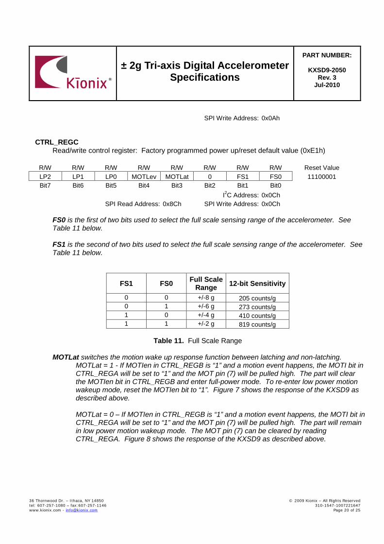
SPI Write Address: 0x0Ah
CTRL_REGC
Read/write control register: Factory programmed power up/reset default value (0xE1h)
R/W R/W R/W R/W R/W R/W R/W R/W Reset Value LP2 LP1 LP0 MOTLev MOTLat 0 FS1 FS0 11100001 Bit7 Bit6 Bit5 Bit4 Bit3 Bit2 Bit1 Bit0
I2C Address: 0x0Ch SPI Read Address: 0x8Ch SPI Write Address: 0x0Ch
FS0 is the first of two bits used to select the full scale sensing range of the accelerometer. See Table 11 below. FS1 is the second of two bits used to select the full scale sensing range of the accelerometer. See Table 11 below.
FS1 FS0 Full Scale Range 12-bit Sensitivity
0 0 +/-8 g 205 counts/g 0 1 +/-6 g 273 counts/g 1 0 +/-4 g 410 counts/g 1 1 +/-2 g 819 counts/g
Table 11. Full Scale Range
MOTLat switches the motion wake up response function between latching and non-latching.
MOTLat = 1 - If MOTIen in CTRL_REGB is “1” and a motion event happens, the MOTI bit in CTRL_REGA will be set to “1” and the MOT pin (7) will be pulled high. The part will clear the MOTIen bit in CTRL_REGB and enter full-power mode. To re-enter low power motion wakeup mode, reset the MOTIen bit to “1”. Figure 7 shows the response of the KXSD9 as described above. MOTLat = 0 – If MOTIen in CTRL_REGB is “1” and a motion event happens, the MOTI bit in CTRL_REGA will be set to “1” and the MOT pin (7) will be pulled high. The part will remain in low power motion wakeup mode. The MOT pin (7) can be cleared by reading CTRL_REGA. Figure 8 shows the response of the KXSD9 as described above.
± 2g Tri-axis Digital Accelerometer
Specifications
PART NUMBER:
KXSD9-2050 Rev. 3
Jul-2010
36 Thornwood Dr. – Ithaca, NY 14850 © 2009 Kionix – All Rights Reserved tel: 607-257-1080 – fax:607-257-1146 310-1547-1007221647 www.kionix.com - [email protected] Page 21 of 25
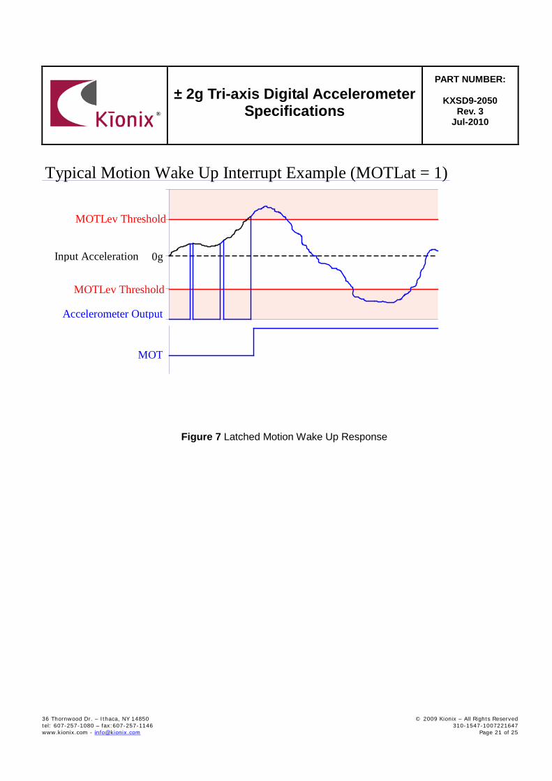
MOTLev Threshold
0g
Typical Motion Wake Up Interrupt Example (MOTLat = 1)
Input Acceleration
MOTLev Threshold
MOT
Accelerometer Output
Figure 7 Latched Motion Wake Up Response

± 2g Tri-axis Digital Accelerometer
Specifications
PART NUMBER:
KXSD9-2050 Rev. 3
Jul-2010
36 Thornwood Dr. – Ithaca, NY 14850 © 2009 Kionix – All Rights Reserved tel: 607-257-1080 – fax:607-257-1146 310-1547-1007221647 www.kionix.com - [email protected] Page 22 of 25
MOTLev Threshold
0g
Typical Motion Wake Up Interrupt Example (MOTLat = 0)
Input Acceleration
MOTLev Threshold
CRTL_REGA Read
MOT
Accelerometer Output
Figure 8 Unlatched Motion Wake Up Response
MOTLev sets the motion wakeup threshold to an acceleration level as defined in Table 12.
MOTLev FS1 FS0 Motion Wake Up Threshold
0 0 0 +/-6 g 0 0 1 +/-4.5 g 0 1 0 +/-3 g 0 1 1 +/-1.5 g 1 0 0 +/-4 g 1 0 1 +/-3 g 1 1 0 +/-2 g 1 1 1 +/-1 g
Table 12. Motion Wake Up Acceleration Threshold
LP0 is the first of three bits used to select the operational bandwidth of the accelerometer. See Table 13 below.

± 2g Tri-axis Digital Accelerometer
Specifications
PART NUMBER:
KXSD9-2050 Rev. 3
Jul-2010
36 Thornwood Dr. – Ithaca, NY 14850 © 2009 Kionix – All Rights Reserved tel: 607-257-1080 – fax:607-257-1146 310-1547-1007221647 www.kionix.com - [email protected] Page 23 of 25
LP1 is the second of three bits used to select the operational bandwidth of the accelerometer. See Table 13 below. LP2 is the third of three bits used to select the operational bandwidth of the accelerometer. See Table 13 below.
LP2 LP1 LP0 Filter Corner Frequency
0 0 0 No Filter 0 0 1 2000 Hz 0 1 0 2000 Hz 0 1 1 2000 Hz 1 0 0 1000 Hz 1 0 1 500 Hz 1 1 0 100 Hz 1 1 1 50 Hz
Table 13. Operational Bandwidth
CTRL_REGB
Read/write control register: Factory programmed power up/reset default value (0x40h)
R/W R/W R/W R/W R/W R/W R/W R/W Reset Value CLKhld ENABLE ST 0 0 MOTIen 0 0 01000000
Bit7 Bit6 Bit5 Bit4 Bit3 Bit2 Bit1 Bit0 I2C Address: 0x0Dh SPI Read Address: 0x8Dh SPI Write Address: 0x0Dh
MOTIen enables the motion wakeup feature.
MOTIen = 1 – the KXSD9 will run in a low power mode until a motion event occurs that causes MOTI in CTRL_REGA and the MOT pin (7) to go high. The part then enters normal operation if MOTLat = 1 or remains in low power mode if MOTLat = 0.
MOTIen = 0 – the KXSD9 is in normal operating mode
ST activates the self-test function for the sensor elements on all three axes. A correctly functioning KXSD9 will increase all channel outputs when Self test = 1 and Enable = 1. This bit can be read or written.
Enable powers up the KXSD9 for operation.
Enable = 1 – normal operation Enable = 0 – low-power standby
CLKhld allows the KXSD9 to hold the serial clock, SCL, low in I2C mode to force the transmitter into a wait state during A/D conversions.

± 2g Tri-axis Digital Accelerometer
Specifications
PART NUMBER:
KXSD9-2050 Rev. 3
Jul-2010
36 Thornwood Dr. – Ithaca, NY 14850 © 2009 Kionix – All Rights Reserved tel: 607-257-1080 – fax:607-257-1146 310-1547-1007221647 www.kionix.com - [email protected] Page 24 of 25
CLKhld = 1 – SCL held low during A/D conversions CLKhld = 0 – SCL unaffected
CLKhld should be set to 0 when Enable is set to 0 (disabled) to prevent potential holding of the CLK line.
CTRL_REGA
Read-only status register
R R R R R R R R X X X X X X MOTI X
Bit7 Bit6 Bit5 Bit4 Bit3 Bit2 Bit1 Bit0 I2C Address: 0x0Eh SPI Read Address: 0x8Eh SPI Write Address: 0x0Eh
MOTI reports the status of the motion wakeup interrupt. Reading CTRL_REGA clears the MOTI bit and MOT pin (7).
MOTI = 1 - a motion wake up event has occurred and the MOT pin (7) is high. MOTI = 0 - a motion wake up event has not occurred and the MOT pin (7) is low.

± 2g Tri-axis Digital Accelerometer
Specifications
PART NUMBER:
KXSD9-2050 Rev. 3
Jul-2010
36 Thornwood Dr. – Ithaca, NY 14850 © 2009 Kionix – All Rights Reserved tel: 607-257-1080 – fax:607-257-1146 310-1547-1007221647 www.kionix.com - [email protected] Page 25 of 25
Revision History REVISION DESCRIPTION DATE 1 Initial release 16-May-
2008 2 Changed to new format & revisioning. 12-Oct-
2009 3 Changed Current Consumption, Operating (15Hz) to Motion Wake Up 15Hz Mode and added typ. and
max fields for it.
08-Jul-2010
"Kionix" is a registered trademark of Kionix, Inc. Products described herein are protected by patents issued or pending. No license is granted by implication or otherwise under any patent or other rights of Kionix. The information contained herein is believed to be accurate and reliable but is not guaranteed. Kionix does not assume responsibility for its use or distribution. Kionix also reserves the right to change product specifications or discontinue this product at any time without prior notice. This publication supersedes and replaces all information previously supplied.