Part 5. Field Effect Transistors - MIT OpenCourseWare · PDF fileIntroduction to...
32
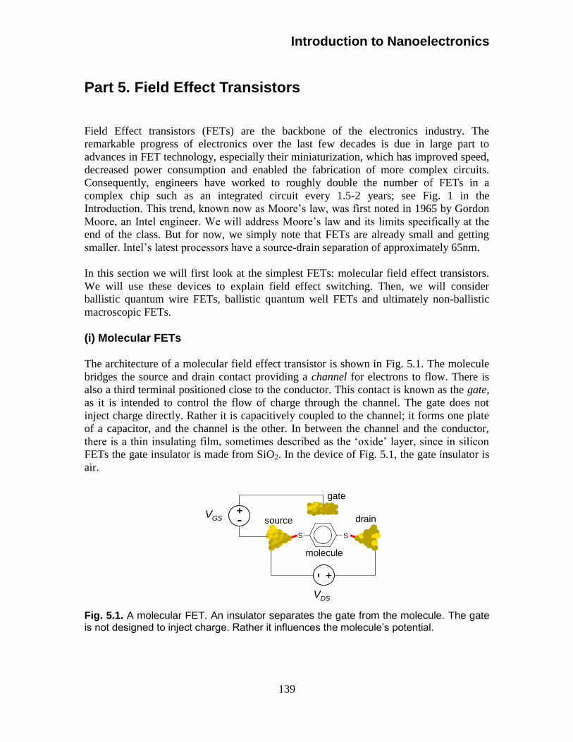
Introduction to Nanoelectronics 139 Part 5. Field Effect Transistors Field Effect transistors (FETs) are the backbone of the electronics industry. The remarkable progress of electronics over the last few decades is due in large part to advances in FET technology, especially their miniaturization, which has improved speed, decreased power consumption and enabled the fabrication of more complex circuits. Consequently, engineers have worked to roughly double the number of FETs in a complex chip such as an integrated circuit every 1.5-2 years; see Fig. 1 in the Introduction. This trend, known now as Moore‟s law, was first noted in 1965 by Gordon Moore, an Intel engineer. We will address Moore‟s law and its limits specifically at the end of the class. But for now, we simply note that FETs are already small and getting smaller. Intel‟s latest processors have a source-drain separation of approximately 65nm. In this section we will first look at the simplest FETs: molecular field effect transistors. We will use these devices to explain field effect switching. Then, we will consider ballistic quantum wire FETs, ballistic quantum well FETs and ultimately non-ballistic macroscopic FETs. (i) Molecular FETs The architecture of a molecular field effect transistor is shown in Fig. 5.1. The molecule bridges the source and drain contact providing a channel for electrons to flow. There is also a third terminal positioned close to the conductor. This contact is known as the gate, as it is intended to control the flow of charge through the channel. The gate does not inject charge directly. Rather it is capacitively coupled to the channel; it forms one plate of a capacitor, and the channel is the other. In between the channel and the conductor, there is a thin insulating film, sometimes described as the „oxide‟ layer, since in silicon FETs the gate insulator is made from SiO 2 . In the device of Fig. 5.1, the gate insulator is air. Fig. 5.1. A molecular FET. An insulator separates the gate from the molecule. The gate is not designed to inject charge. Rather it influences the molecule‟s potential. S S + - + - V DS source drain molecule + - + - V GS gate
Transcript of Part 5. Field Effect Transistors - MIT OpenCourseWare · PDF fileIntroduction to...
Introduction to Nanoelectronics
139
Part 5. Field Effect Transistors
Field Effect transistors (FETs) are the backbone of the electronics industry. The
remarkable progress of electronics over the last few decades is due in large part to
advances in FET technology, especially their miniaturization, which has improved speed,
decreased power consumption and enabled the fabrication of more complex circuits.
Consequently, engineers have worked to roughly double the number of FETs in a
complex chip such as an integrated circuit every 1.5-2 years; see Fig. 1 in the
Introduction. This trend, known now as Moore‟s law, was first noted in 1965 by Gordon
Moore, an Intel engineer. We will address Moore‟s law and its limits specifically at the
end of the class. But for now, we simply note that FETs are already small and getting
smaller. Intel‟s latest processors have a source-drain separation of approximately 65nm.
In this section we will first look at the simplest FETs: molecular field effect transistors.
We will use these devices to explain field effect switching. Then, we will consider
ballistic quantum wire FETs, ballistic quantum well FETs and ultimately non-ballistic
macroscopic FETs.
(i) Molecular FETs
The architecture of a molecular field effect transistor is shown in Fig. 5.1. The molecule
bridges the source and drain contact providing a channel for electrons to flow. There is
also a third terminal positioned close to the conductor. This contact is known as the gate,
as it is intended to control the flow of charge through the channel. The gate does not
inject charge directly. Rather it is capacitively coupled to the channel; it forms one plate
of a capacitor, and the channel is the other. In between the channel and the conductor,
there is a thin insulating film, sometimes described as the „oxide‟ layer, since in silicon
FETs the gate insulator is made from SiO2. In the device of Fig. 5.1, the gate insulator is
air.
Fig. 5.1. A molecular FET. An insulator separates the gate from the molecule. The gate is not designed to inject charge. Rather it influences the molecule‟s potential.
S S
+- +-
VDS
source drain
molecule
+-+-
VGS
gate
Part 5. Field Effect Transistors
140
0
0.5
1
1.5
2
2.5
0
0.5
1
1.5
2
2.5
I DS
(nA
)
5 5.5 6 6.5 7 7.55 5.5 6 6.5 7 7.50
0.1
0.2
0.3
0.4
0.5
0.6
0.7
0.8
0
0.1
0.2
0.3
0.4
0.5
0.6
0.7
0.8
I DS
(A
)
VGS (V)
VDS=10mV
G=10meV
G=10eV
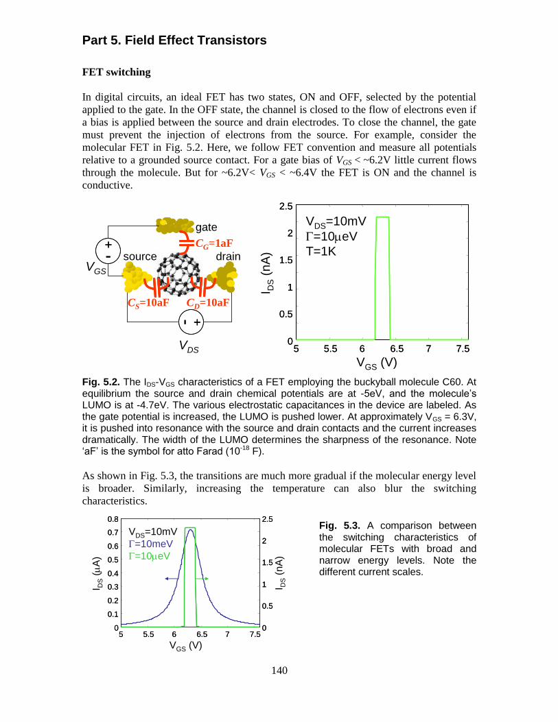
FET switching
In digital circuits, an ideal FET has two states, ON and OFF, selected by the potential
applied to the gate. In the OFF state, the channel is closed to the flow of electrons even if
a bias is applied between the source and drain electrodes. To close the channel, the gate
must prevent the injection of electrons from the source. For example, consider the
molecular FET in Fig. 5.2. Here, we follow FET convention and measure all potentials
relative to a grounded source contact. For a gate bias of VGS < ~6.2V little current flows
through the molecule. But for ~6.2V< VGS < ~6.4V the FET is ON and the channel is
conductive.
Fig. 5.2. The IDS-VGS characteristics of a FET employing the buckyball molecule C60. At equilibrium the source and drain chemical potentials are at -5eV, and the molecule‟s LUMO is at -4.7eV. The various electrostatic capacitances in the device are labeled. As the gate potential is increased, the LUMO is pushed lower. At approximately VGS = 6.3V, it is pushed into resonance with the source and drain contacts and the current increases dramatically. The width of the LUMO determines the sharpness of the resonance. Note „aF‟ is the symbol for atto Farad (10-18 F).
As shown in Fig. 5.3, the transitions are much more gradual if the molecular energy level
is broader. Similarly, increasing the temperature can also blur the switching
characteristics.
Fig. 5.3. A comparison between the switching characteristics of molecular FETs with broad and narrow energy levels. Note the different current scales.
0
0.5
1
1.5
2
2.5
0
0.5
1
1.5
2
2.5
5 5.5 6 6.5 7 7.55 5.5 6 6.5 7 7.5
I DS
(nA
)
VGS (V)
VDS=10mV
G=10eV
T=1K
+- +-
VDS
source drain+-+-
VGS
gate
CG=1aF
CS=10aF CD=10aF
Introduction to Nanoelectronics
141
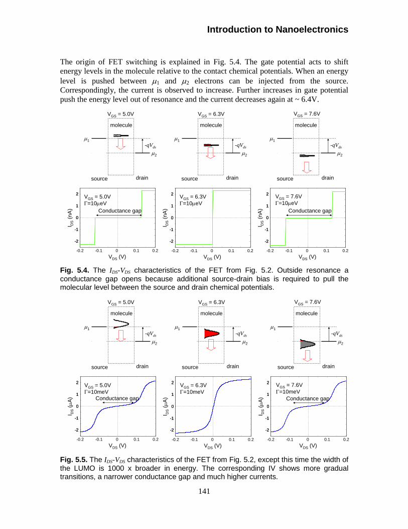
The origin of FET switching is explained in Fig. 5.4. The gate potential acts to shift
energy levels in the molecule relative to the contact chemical potentials. When an energy
level is pushed between 1 and 2 electrons can be injected from the source.
Correspondingly, the current is observed to increase. Further increases in gate potential
push the energy level out of resonance and the current decreases again at ~ 6.4V.
Fig. 5.4. The IDS-VDS characteristics of the FET from Fig. 5.2. Outside resonance a
conductance gap opens because additional source-drain bias is required to pull the molecular level between the source and drain chemical potentials.
Fig. 5.5. The IDS-VDS characteristics of the FET from Fig. 5.2, except this time the width of
the LUMO is 1000 x broader in energy. The corresponding IV shows more gradual transitions, a narrower conductance gap and much higher currents.
1
2
-qVds
source drain
molecule
1
2
-qVds
source drain
molecule
1
2
-qVds
source drain
molecule
-0.2 -0.1 0 0.1 0.2
-2
-1
0
1
2
-2
-1
0
1
2
I DS
(nA
)
VDS (V)-0.2 -0.1 0 0.1 0.2
-2
-1
0
1
2
-2
-1
0
1
2
I DS
(nA
)
VDS (V)
VGS = 6.3V
G=10eV
VGS = 5.0V
G=10eV
-0.2 -0.1 0 0.1 0.2
-2
-1
0
1
2
-2
-1
0
1
2
I DS
(nA
)VDS (V)
VGS = 7.6V
G=10eV
VGS = 6.3VVGS = 5.0V VGS = 7.6V
Conductance gap Conductance gap
1
2
-qVds
source drain
molecule
1
2
-qVds
source drain
molecule
1
2
-qVds
source drain
molecule
-0.2 -0.1 0 0.1 0.2
-2
-1
0
1
2
-2
-1
0
1
2
I DS
(A
)
VDS (V)-0.2 -0.1 0 0.1 0.2
-2
-1
0
1
2
-2
-1
0
1
2
I DS
(A
)
VDS (V)
VGS = 6.3V
G=10meV
VGS = 5.0V
G=10meV
-0.2 -0.1 0 0.1 0.2
-2
-1
0
1
2
-2
-1
0
1
2
I DS
(A
)
VDS (V)
VGS = 7.6V
G=10meV
VGS = 6.3VVGS = 5.0V VGS = 7.6V
Conductance gapConductance gap
Part 5. Field Effect Transistors
142
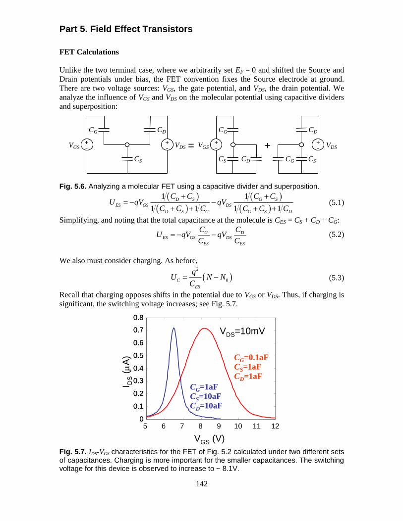
FET Calculations
Unlike the two terminal case, where we arbitrarily set EF = 0 and shifted the Source and
Drain potentials under bias, the FET convention fixes the Source electrode at ground.
There are two voltage sources: VGS, the gate potential, and VDS, the drain potential. We
analyze the influence of VGS and VDS on the molecular potential using capacitive dividers
and superposition:
Fig. 5.6. Analyzing a molecular FET using a capacitive divider and superposition.
1 1
1 1 1 1
D S G S
ES GS DS
D S G G S D
C C C CU qV qV
C C C C C C
(5.1)
Simplifying, and noting that the total capacitance at the molecule is CES = CS + CD + CG:
G DES GS DS
ES ES
C CU qV qV
C C (5.2)
We also must consider charging. As before,
2
0C
ES
qU N N
C (5.3)
Recall that charging opposes shifts in the potential due to VGS or VDS. Thus, if charging is
significant, the switching voltage increases; see Fig. 5.7.
Fig. 5.7. IDS-VGS characteristics for the FET of Fig. 5.2 calculated under two different sets
of capacitances. Charging is more important for the smaller capacitances. The switching voltage for this device is observed to increase to ~ 8.1V.
= +VGS+- VDS
CS
CD
CGCS CD
CG
VGS+- VDS+-
CD
CS
+-+-
CG
+-+-
+-
5 6 7 8 9 10 11 120
0.1
0.2
0.3
0.4
0.5
0.6
0.7
0.8
0
0.1
0.2
0.3
0.4
0.5
0.6
0.7
0.8
I DS
(A
)
VGS (V)
VDS=10mV
CG=0.1aF
CS=1aF
CD=1aF
CG=1aF
CS=10aF
CD=10aF
Introduction to Nanoelectronics
143
Adding the static potential due to VDS and VGS gives, the potential U in terms of the
charge, N, and bias
2
0G D
GS DS
ES ES ES
C C qU qV qV N N
C C C (5.4)
We also have an expression for potential for N in terms of U (see Eq. (3.31))
, ,D S S D
S D
f E f EN g E U dE
(5.5)
As before, Eqns. (5.4) and (5.5) must typically be solved iteratively to obtain U. Then we
can solve for the current using:
1
, ,S D
S D
I q g E U f E f E dE
(5.6)
Quantum Capacitance in FETs
Unfortunately, Eqns. (5.4) and (5.5) typically must be solved iteratively. But insight can
be gained by studying a FET with a few approximations.
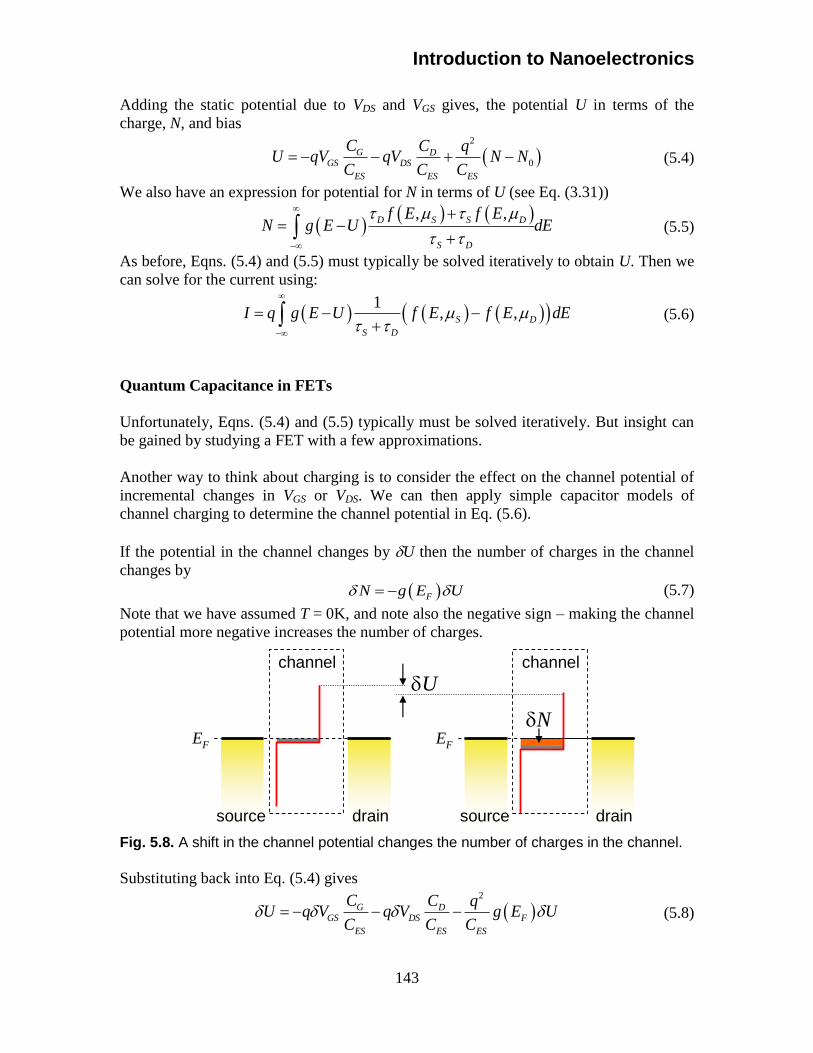
Another way to think about charging is to consider the effect on the channel potential of
incremental changes in VGS or VDS. We can then apply simple capacitor models of
channel charging to determine the channel potential in Eq. (5.6).
If the potential in the channel changes by U then the number of charges in the channel
changes by
FN g E U (5.7)
Note that we have assumed T = 0K, and note also the negative sign – making the channel
potential more negative increases the number of charges.
Fig. 5.8. A shift in the channel potential changes the number of charges in the channel.
Substituting back into Eq. (5.4) gives
2
G DGS DS F
ES ES ES
C C qU q V q V g E U
C C C (5.8)
N
channel
EF
source drain
channel
EF
source drain
U
Part 5. Field Effect Transistors
144
Collecting U terms gives
G DGS DS
ES Q ES Q
C CU q V q V
C C C C
(5.9)
Where we recall the quantum capacitance (CQ):
2
Q FC q g E (5.10)
Using the quantum capacitance, we can easily construct a small signal model for changes
in VGS or VDS. See, for example the small signal VGS model in Fig. 5.9. Note that the value
of the quantum capacitance depends on the channel potential at the bias point.
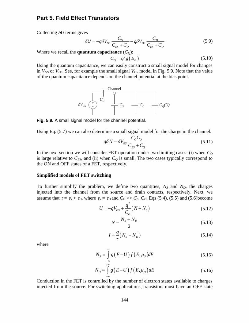
Fig. 5.9. A small signal model for the channel potential.
Using Eq. (5.7) we can also determine a small signal model for the charge in the channel.
G Q
GS
ES Q
C Cq N V
C C
(5.11)
In the next section we will consider FET operation under two limiting cases: (i) when CQ
is large relative to CES, and (ii) when CQ is small. The two cases typically correspond to
the ON and OFF states of a FET, respectively.
Simplified models of FET switching
To further simplify the problem, we define two quantities, NS and ND, the charges
injected into the channel from the source and drain contacts, respectively. Next, we
assume that = S + D, where S = D and CG >> CS, CD, Eqs (5.4), (5.5) and (5.6)become
2
0GS
G
qU qV N N
C (5.12)
2
S DN NN
(5.13)
S D
qI N N
(5.14)
where
,S SN g E U f E dE
(5.15)
,D DN g E U f E dE
(5.16)
Conduction in the FET is controlled by the number of electron states available to charges
injected from the source. For switching applications, transistors must have an OFF state
CS CDVGS
CG
Channel
+- CQ(U)
Introduction to Nanoelectronics
145
where IDS is ideally forced to zero. The OFF state is realized by minimizing the number
of empty states in the channel accessible to electrons from the source. In the limit that
there are no available states, the channel is a perfect insulator.
Switching between ON and OFF states is achieved by using the gate to push empty
channel states towards the source chemical potential. The transition between ON and
OFF states is known as the threshold. Although the transition is not sharp in every
channel material, it is convenient to define a gate bias known as the threshold voltage, VT,
where the density of states at the source chemical potential g(EF) undergoes a transition.
The Zero Charging limit
As we saw in Part 3, charging-induced shifts in the energy levels of conductors can
significantly complicate the calculation of IV characteristics. Equation (5.11)
demonstrates that charging can be neglected if the quantum capacitance is much smaller
than the electrostatic capacitance, i.e. CQ << CES. For example, in Eq. (5.11), if CQ << CES
then the charging, N → 0.
In the zero charging limit, Eq. (5.12) reduces to
GSU qV (5.17)
i.e. in this limit the channel potential simply tracks the gate bias.
Thus, in the zero charging limit, we can determine the current directly from Eq. (5.6),
with the channel potential U = -qVGS.
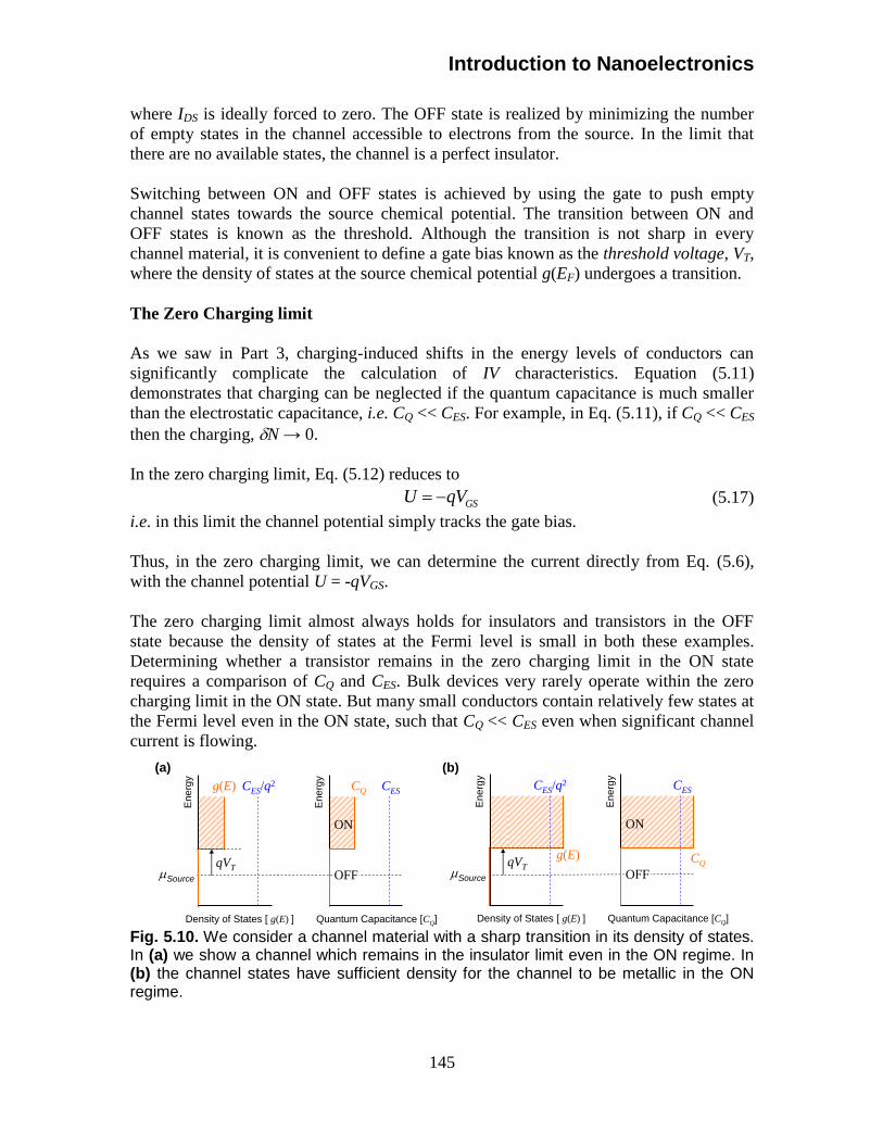
The zero charging limit almost always holds for insulators and transistors in the OFF
state because the density of states at the Fermi level is small in both these examples.
Determining whether a transistor remains in the zero charging limit in the ON state
requires a comparison of CQ and CES. Bulk devices very rarely operate within the zero
charging limit in the ON state. But many small conductors contain relatively few states at
the Fermi level even in the ON state, such that CQ << CES even when significant channel
current is flowing.
Fig. 5.10. We consider a channel material with a sharp transition in its density of states. In (a) we show a channel which remains in the insulator limit even in the ON regime. In (b) the channel states have sufficient density for the channel to be metallic in the ON regime.
En
erg
y
Source
Density of States [ g(E) ]
g(E)
qVT
ON
CES/q2
En
erg
y
Quantum Capacitance [CQ]
CQ CES
OFF
En
erg
y
Source
Density of States [ g(E) ]
g(E)qVT
ON
CES/q2
En
erg
y
Quantum Capacitance [CQ]
CQ
CES
OFF
(a) (b)
Part 5. Field Effect Transistors
146
S
D
E
electron
chargingPinch off
-q(VGS – VT)
Zero charging
limit
The Strong Charging Limit
In metals and many large transistors in the ON state, the density of states at the Fermi
level is sufficiently large that adding charges barely moves the channel potential. We say
that the Fermi level is pinned. In the limit that g(EF) → ∞ then DU → 0.
In terms of the quantum capacitance, we find that if CQ >> CES, Eq. (5.11) reduces to
GS Gq N V C (5.18)
This limit is also known as strong inversion in conventional FET analysis. The channel
transforms from an insulator to a metal. The transition occurs when the gate bias equals
the threshold voltage, VT, which is defined as the gate bias required to push the channel
energy level down to the source workfunction.
In the strong charging/metallic limit, the gate and channel act as two plates of a capacitor.
The charge in the channel then changes linearly with additional gate bias. In FETs, the
channel potential relative to the source, V(x), may also vary with position. Including the
channel potential and the threshold voltage in Eq. (5.18) yields:
G GS TqN C V V V x (5.19)
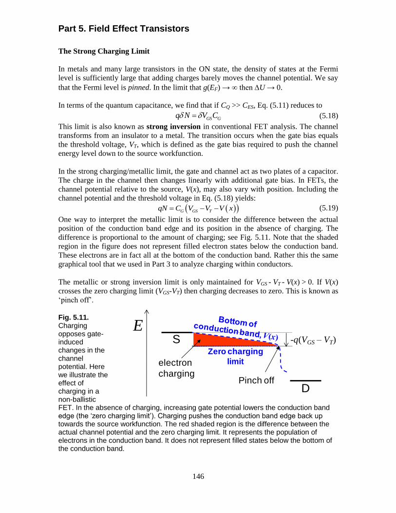
One way to interpret the metallic limit is to consider the difference between the actual
position of the conduction band edge and its position in the absence of charging. The
difference is proportional to the amount of charging; see Fig. 5.11. Note that the shaded
region in the figure does not represent filled electron states below the conduction band.
These electrons are in fact all at the bottom of the conduction band. Rather this the same
graphical tool that we used in Part 3 to analyze charging within conductors.
The metallic or strong inversion limit is only maintained for VGS - VT - V(x) > 0. If V(x)
crosses the zero charging limit (VGS-VT) then charging decreases to zero. This is known as
„pinch off‟.
Fig. 5.11. Charging opposes gate-induced changes in the channel potential. Here we illustrate the effect of charging in a non-ballistic FET. In the absence of charging, increasing gate potential lowers the conduction band edge (the „zero charging limit‟). Charging pushes the conduction band edge back up towards the source workfunction. The red shaded region is the difference between the actual channel potential and the zero charging limit. It represents the population of electrons in the conduction band. It does not represent filled states below the bottom of the conduction band.
Introduction to Nanoelectronics
147
Ene
rgy
Density of States [ g(E) ]
g(E)f(E,) ~ e-(E-)/kT
f(E,)=1+ e(E-)/kT
1f(E,)=1+ e(E-)/kT
1
filled states
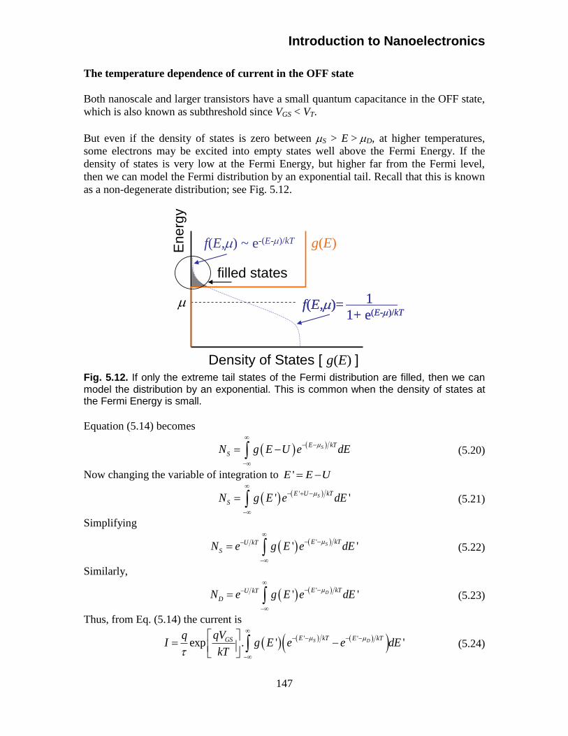
The temperature dependence of current in the OFF state
Both nanoscale and larger transistors have a small quantum capacitance in the OFF state,
which is also known as subthreshold since VGS < VT.
But even if the density of states is zero between S > E > D, at higher temperatures,
some electrons may be excited into empty states well above the Fermi Energy. If the
density of states is very low at the Fermi Energy, but higher far from the Fermi level,
then we can model the Fermi distribution by an exponential tail. Recall that this is known
as a non-degenerate distribution; see Fig. 5.12.
Fig. 5.12. If only the extreme tail states of the Fermi distribution are filled, then we can model the distribution by an exponential. This is common when the density of states at the Fermi Energy is small.
Equation (5.14) becomes
SE kT
SN g E U e dE
(5.20)
Now changing the variable of integration to 'E E U
'' 'SE U kT
SN g E e dE
(5.21)
Simplifying
'' 'SE kTU kT
SN e g E e dE
(5.22)
Similarly,
'' 'DE kTU kT
DN e g E e dE
(5.23)
Thus, from Eq. (5.14) the current is
' 'exp . ' 'S DE kT E kTGSqVq
I g E e e dEkT
(5.24)
Part 5. Field Effect Transistors
148
0 0.1 0.2 0.3 0.4 0.5 0.6
CG = 1000aF
CS = 10aF
CD = 10aF
VDS = 10mV
G = 0.1meV
T = 298K
T = 1K
I DS(A
)
VGS (V)
10-12
10-11
10-10
10-9
10-8
10-7
60 mV/decade
Equation (5.24) holds in the limit that CG >> CS, CD. In general, we find that the current
in the subthreshold region is
0 exp GS G
ES
qV CI I
kT C
(5.25)
Taking logarithm of both sides we find,
10 10 10 0log log logGGS
ES
CqI e V I
kT C (5.26)
The slope, S, of the subthreshold regime is usually expressed gate volts per decade of
drain current. At room temperature, the optimum, when CG >> CS, CD, is
10
160 mV/decade
log
kTS
q e (5.27)
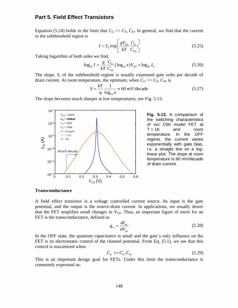
The slope becomes much sharper at low temperatures; see Fig. 5.13.
Fig. 5.13. A comparison of the switching characteristics of our C60 model FET at T = 1K and room temperature. In the OFF regime, the current varies exponentially with gate bias, i.e. a straight line on a log-linear plot. The slope at room temperature is 60 mV/decade of drain current.
Transconductance
A field effect transistor is a voltage controlled current source. Its input is the gate
potential, and the output is the source-drain current. In applications, we usually desire
that the FET amplifies small changes in VGS. Thus, an important figure of merit for an
FET is the transconductance, defined as
dsm
gs
dIg
dV (5.28)
In the OFF state, the quantum capacitance is small and the gate‟s only influence on the
FET is its electrostatic control of the channel potential. From Eq. (5.1), we see that this
control is maximized when
,G S DC C C (5.29)
This is an important design goal for FETs. Under this limit the transconductance is
commonly expressed as:
Introduction to Nanoelectronics
149
+- +-
VDS
+-+-
VGS
gate<< 1nm
~1nm
1m ds
ds ds gs
g dI q
I I dV kT (5.30)
Good electrostatic control of the channel may be achieved either by increasing the
dielectric constant of the gate insulator, or by reducing the thickness of the gate insulator.
A good rule of thumb is that the gate must be much closer to the channel than either the
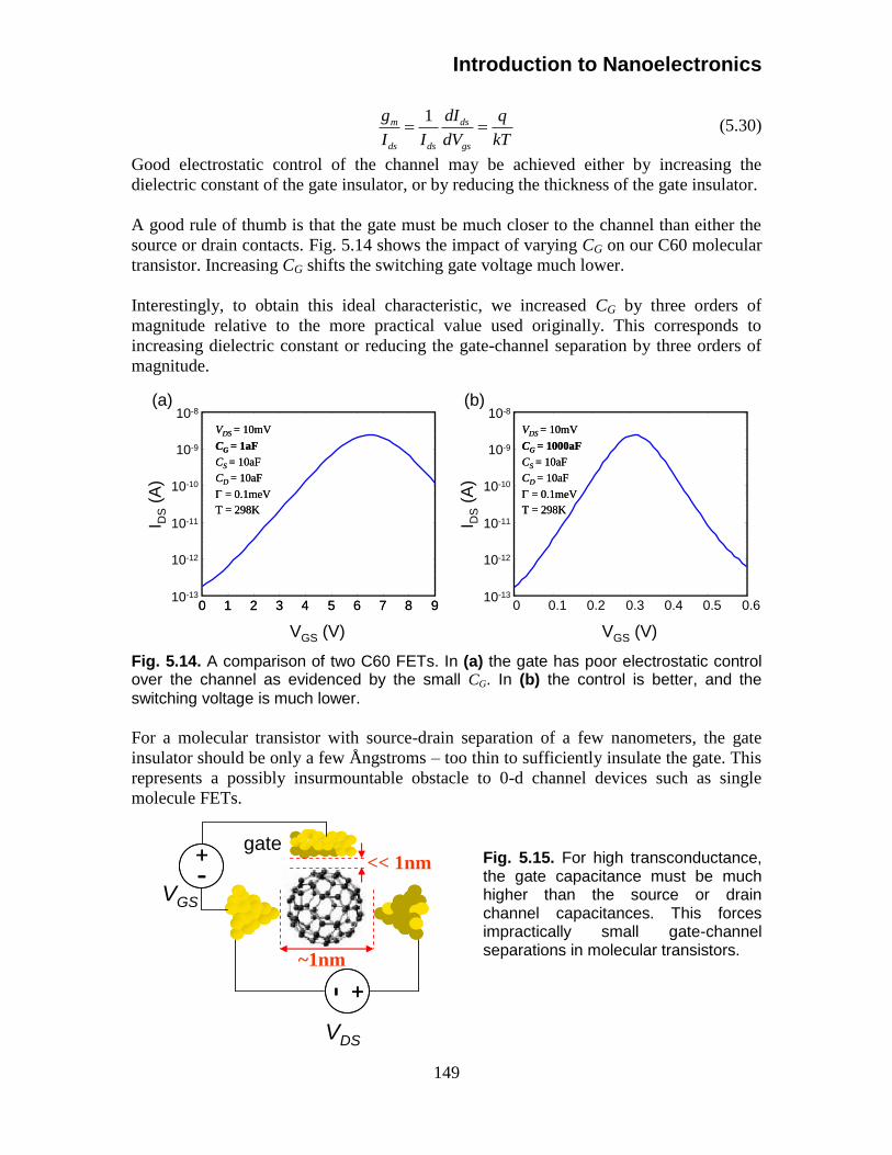
source or drain contacts. Fig. 5.14 shows the impact of varying CG on our C60 molecular
transistor. Increasing CG shifts the switching gate voltage much lower.
Interestingly, to obtain this ideal characteristic, we increased CG by three orders of
magnitude relative to the more practical value used originally. This corresponds to
increasing dielectric constant or reducing the gate-channel separation by three orders of
magnitude.
Fig. 5.14. A comparison of two C60 FETs. In (a) the gate has poor electrostatic control over the channel as evidenced by the small CG. In (b) the control is better, and the
switching voltage is much lower.
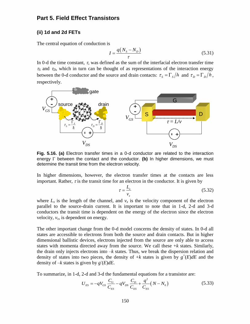
For a molecular transistor with source-drain separation of a few nanometers, the gate
insulator should be only a few Ångstroms – too thin to sufficiently insulate the gate. This
represents a possibly insurmountable obstacle to 0-d channel devices such as single
molecule FETs.
Fig. 5.15. For high transconductance, the gate capacitance must be much higher than the source or drain channel capacitances. This forces impractically small gate-channel separations in molecular transistors.
I DS
(A)
VGS (V)
10-13
10-12
10-11
10-10
10-9
10-8
0 1 2 3 4 5 6 7 8 90 1 2 3 4 5 6 7 8 9
(a)
CG = 1aF
CS = 10aF
CD = 10aF
VDS = 10mV
G = 0.1meV
T = 298K
CG = 1aF
CS = 10aF
CD = 10aF
VDS = 10mV
G = 0.1meV
T = 298K
I DS
(A)
VGS (V)
10-13
10-12
10-11
10-10
10-9
10-8(b)
CG = 1000aF
CS = 10aF
CD = 10aF
VDS = 10mV
G = 0.1meV
T = 298K
CG = 1000aF
CS = 10aF
CD = 10aF
VDS = 10mV
G = 0.1meV
T = 298K
0 0.1 0.2 0.3 0.4 0.5 0.6
Part 5. Field Effect Transistors
150
(ii) 1d and 2d FETs
The central equation of conduction is
S Dq N N
I
(5.31)
In 0-d the time constant, , was defined as the sum of the interfacial electron transfer time
S and D, which in turn can be thought of as representations of the interaction energy
between the 0-d conductor and the source and drain contacts: S S G and D D G ,
respectively.
Fig. 5.16. (a) Electron transfer times in a 0-d conductor are related to the interaction
energy G between the contact and the conductor. (b) In higher dimensions, we must determine the transit time from the electron velocity.
In higher dimensions, however, the electron transfer times at the contacts are less
important. Rather, is the transit time for an electron in the conductor. It is given by
x
x
L
v (5.32)
where Lx is the length of the channel, and vx is the velocity component of the electron
parallel to the source-drain current. It is important to note that in 1-d, 2-d and 3-d
conductors the transit time is dependent on the energy of the electron since the electron
velocity, vx, is dependent on energy.
The other important change from the 0-d model concerns the density of states. In 0-d all
states are accessible to electrons from both the source and drain contacts. But in higher
dimensional ballistic devices, electrons injected from the source are only able to access
states with momenta directed away from the source. We call these +k states. Similarly,
the drain only injects electrons into –k states. Thus, we break the dispersion relation and
density of states into two pieces, the density of +k states is given by g+(E)dE and the
density of –k states is given by g-(E)dE.
To summarize, in 1-d, 2-d and 3-d the fundamental equations for a transistor are:
2
0G D
ES GS DS
ES ES ES
C C qU qV qV N N
C C C (5.33)
+- +-
VDS
source drain+-+-
VGS
gate
G
S D
= L/v
+- +-
VDS
+-+-
VGSS
SG
DD
G
Introduction to Nanoelectronics
151
kz
E
EC
DOS
E
EC
S DN N N (5.34)
S D
qI N N
(5.35)
where
,S SN g E U f E dE
(5.36)
,D DN g E U f E dE
(5.37)
The ballistic quantum wire FET.†
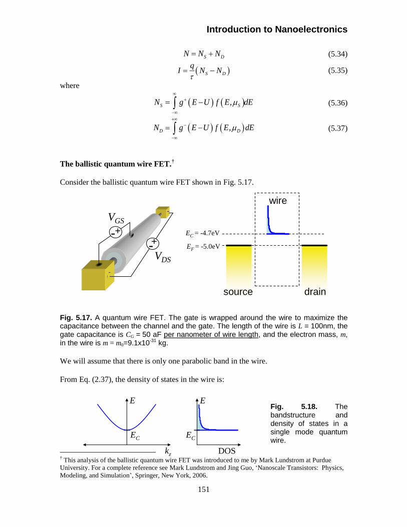
Consider the ballistic quantum wire FET shown in Fig. 5.17.
Fig. 5.17. A quantum wire FET. The gate is wrapped around the wire to maximize the capacitance between the channel and the gate. The length of the wire is L = 100nm, the gate capacitance is CG = 50 aF per nanometer of wire length, and the electron mass, m, in the wire is m = m0=9.1x10⁻³¹ kg.
We will assume that there is only one parabolic band in the wire.
From Eq. (2.37), the density of states in the wire is:
Fig. 5.18. The bandstructure and density of states in a single mode quantum wire.
† This analysis of the ballistic quantum wire FET was introduced to me by Mark Lundstrom at Purdue
University. For a complete reference see Mark Lundstrom and Jing Guo, „Nanoscale Transistors: Physics,
Modeling, and Simulation‟, Springer, New York, 2006.
+-
VDS
wire
EF = -5.0eV
EC = -4.7eV
source drain
VGS+-
Part 5. Field Effect Transistors
152
2 2
C
C
L mg E dE u E E dE
h E E
, (5.38)
where L is the length of the wire, and m is the electron mass in the wire. But only half of
these states contain electrons traveling in the positive direction. Thus, we must divide Eq.
(5.38) by two to yield:
1 2 2
2C
C
L mg E dE u E E dE
h E E
(5.39)
Given the position of the Fermi Energy, this band is the conduction band. We will label
the energy at the bottom of the conduction band, EC. Since we model electrons moving
along the wire as plane waves, within the parabolic band we have
2 2
21
2 2C
kE E mv
m (5.40)
We can rewrite Eq. (5.39) in terms of the velocity, v, of the electron:
1 4
2C
Lg E dE u E E dE
hv E
(5.41)
Now L/v is the transit time of an electron through the wire, thus
41
2C
Eg E dE u E E dE
h
. (5.42)
We can substitute Eq. (5.42) into the expression for the current density (Eq. (5.31)) to
obtain
2
, ,C S D
qI u E E U f E f E dE
h
. (5.43)
Quantum dot models of quantum wire transistor channels
Under bias we expect a spatial variation in the potential along a quantum wire. Current
flow may also vary the charge density along the wire, which in turn affects the potential
profile. Thus, the potential variation must be determined self consistently with the current
flow.
We have seen in Part 4 that the conduction band edge in a ballistic conductor is
determined by the point of maximum potential in the conductor. For electrostatic
purposes, we will approximate this point on the quantum wire as a quantum dot, and then
employ our discrete capacitive models of potential to calculate changes in the conduction
band edge.
Usually the highest potential is located next to the source, because application of forward
bias at the drain pulls the potential down along the channel.
Introduction to Nanoelectronics
153
-5.0 -4.9 -4.8 -4.7 -4.6 -4.50.01
0.1
1
10
0.01
0.1
1
10
CES
CQ
Capacitance (
fF)
Energy (eV)
S
DVDS
E
position
Source
contact
Drain
contact
„Quantum dot‟
S D
Increasing gate
potential
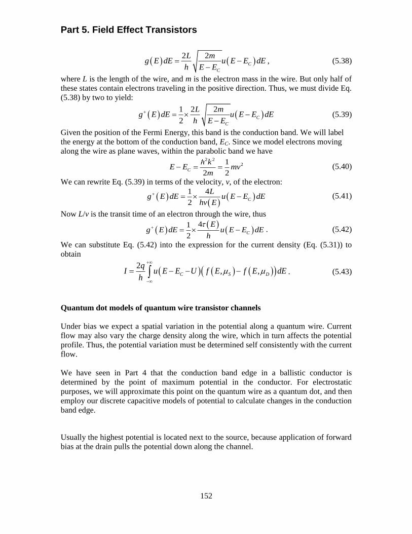
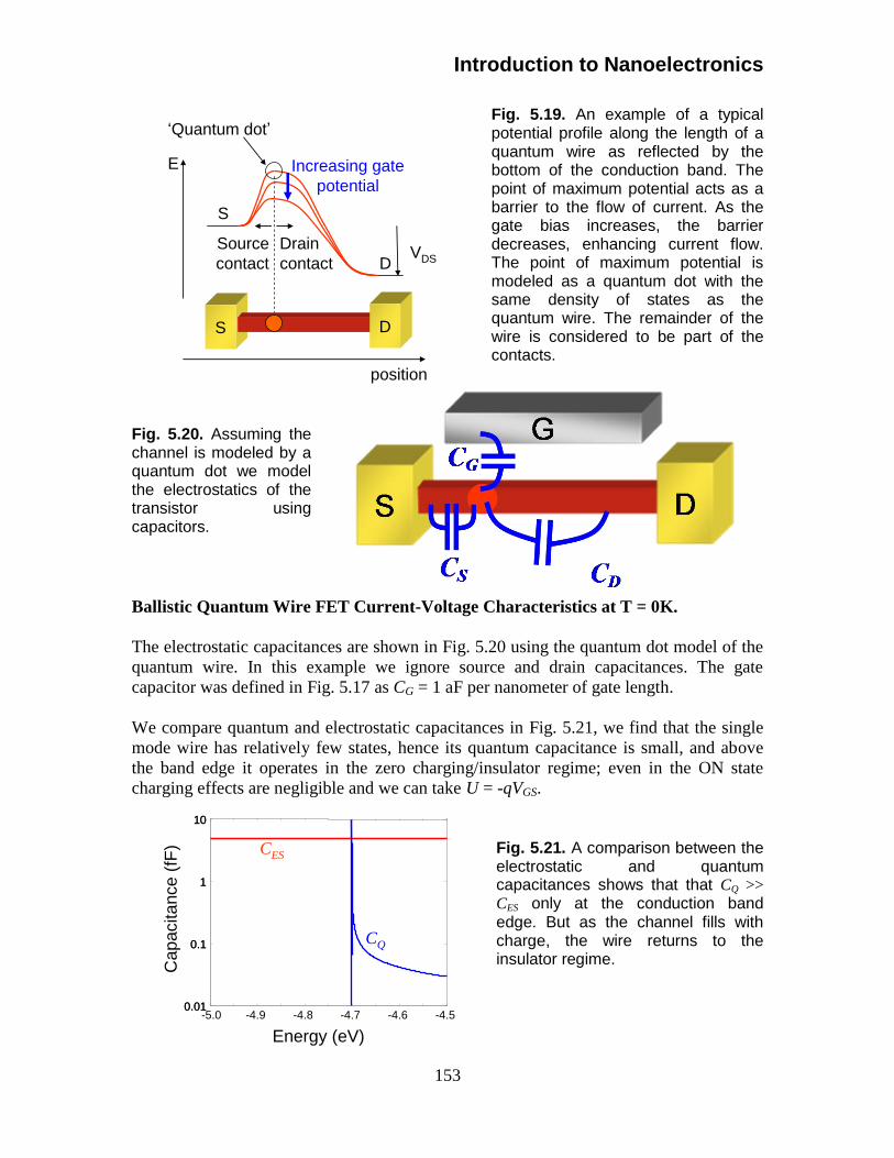
Fig. 5.19. An example of a typical potential profile along the length of a quantum wire as reflected by the bottom of the conduction band. The point of maximum potential acts as a barrier to the flow of current. As the gate bias increases, the barrier decreases, enhancing current flow. The point of maximum potential is modeled as a quantum dot with the same density of states as the quantum wire. The remainder of the wire is considered to be part of the contacts.
Fig. 5.20. Assuming the channel is modeled by a quantum dot we model the electrostatics of the transistor using capacitors.
Ballistic Quantum Wire FET Current-Voltage Characteristics at T = 0K.
The electrostatic capacitances are shown in Fig. 5.20 using the quantum dot model of the
quantum wire. In this example we ignore source and drain capacitances. The gate
capacitor was defined in Fig. 5.17 as CG = 1 aF per nanometer of gate length.
We compare quantum and electrostatic capacitances in Fig. 5.21, we find that the single
mode wire has relatively few states, hence its quantum capacitance is small, and above
the band edge it operates in the zero charging/insulator regime; even in the ON state
charging effects are negligible and we can take U = -qVGS.
Fig. 5.21. A comparison between the electrostatic and quantum capacitances shows that that CQ >>
CES only at the conduction band edge. But as the channel fills with charge, the wire returns to the insulator regime.
Part 5. Field Effect Transistors
154
wire
EF=-5.0eV
EC=-4.7eV
source
drain
VT
wire
EF
source
drain
EC - qVGS
qVDS
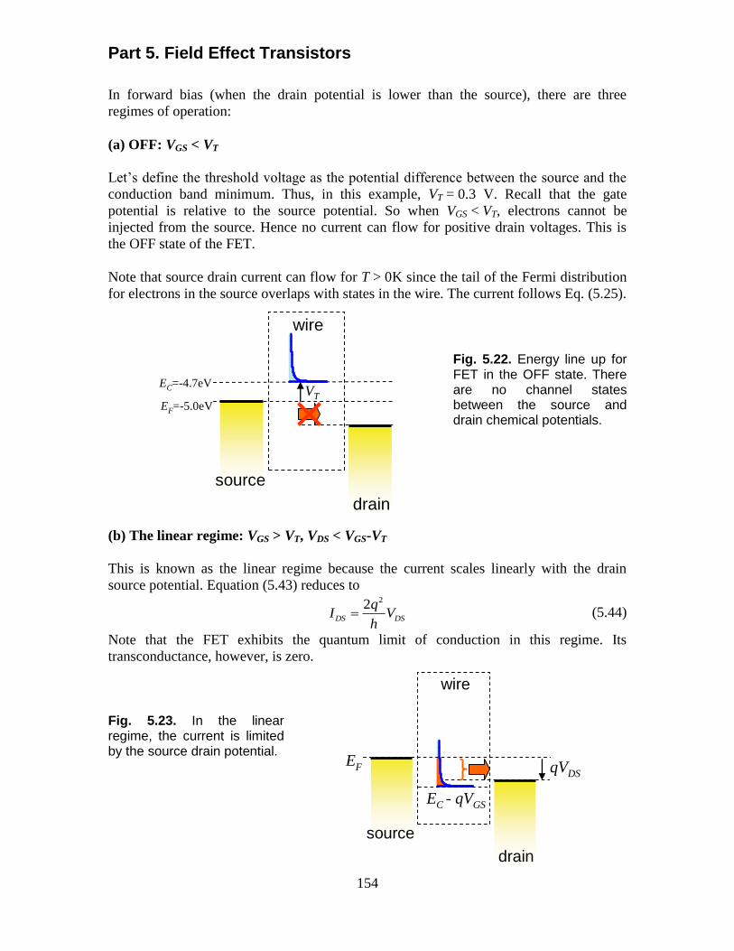
In forward bias (when the drain potential is lower than the source), there are three
regimes of operation:
(a) OFF: VGS < VT
Let‟s define the threshold voltage as the potential difference between the source and the
conduction band minimum. Thus, in this example, VT = 0.3 V. Recall that the gate
potential is relative to the source potential. So when VGS < VT, electrons cannot be
injected from the source. Hence no current can flow for positive drain voltages. This is
the OFF state of the FET.
Note that source drain current can flow for T > 0K since the tail of the Fermi distribution
for electrons in the source overlaps with states in the wire. The current follows Eq. (5.25).
Fig. 5.22. Energy line up for FET in the OFF state. There are no channel states between the source and drain chemical potentials.
(b) The linear regime: VGS > VT, VDS < VGS-VT
This is known as the linear regime because the current scales linearly with the drain
source potential. Equation (5.43) reduces to
22
DS DS
qI V
h (5.44)
Note that the FET exhibits the quantum limit of conduction in this regime. Its
transconductance, however, is zero.
Fig. 5.23. In the linear regime, the current is limited by the source drain potential.
Introduction to Nanoelectronics
155
wire
EF
source
drain
qVDS
EC - qVGS
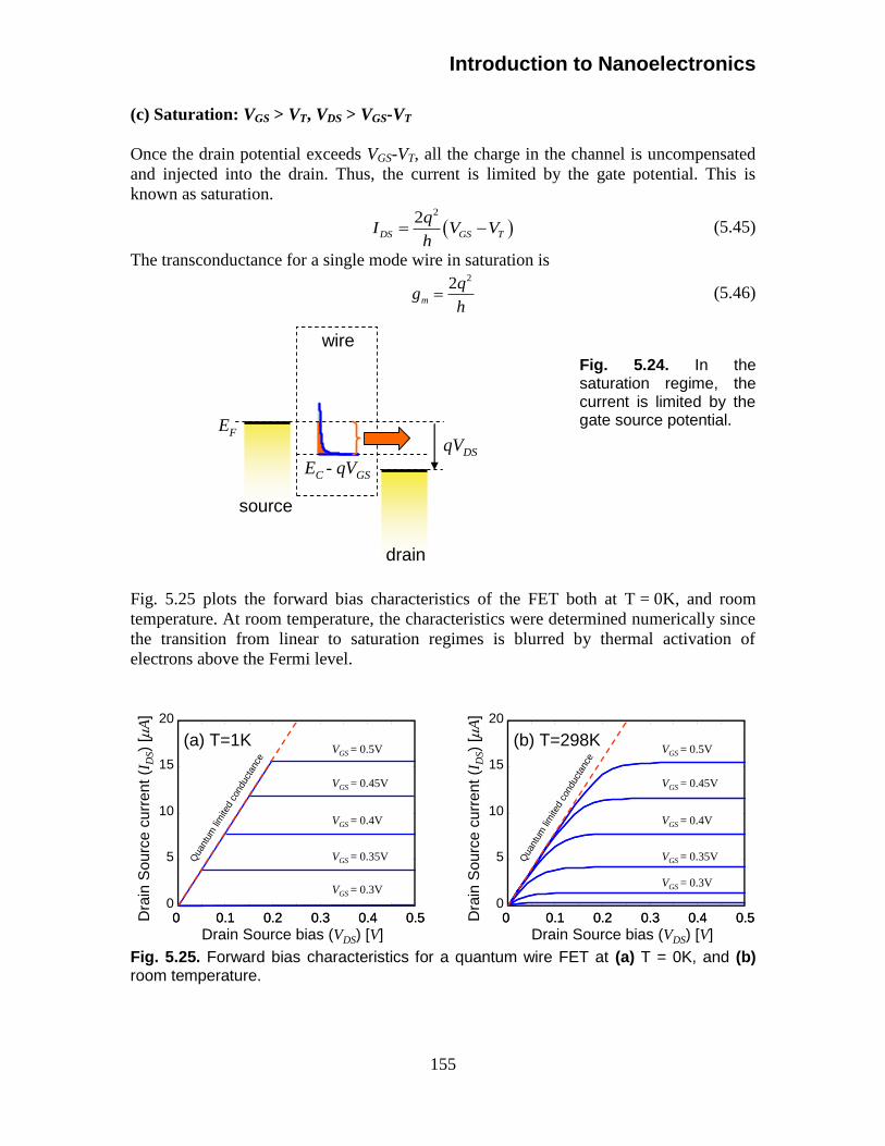
(c) Saturation: VGS > VT, VDS > VGS-VT
Once the drain potential exceeds VGS-VT, all the charge in the channel is uncompensated
and injected into the drain. Thus, the current is limited by the gate potential. This is
known as saturation.
22
DS GS T
qI V V
h (5.45)
The transconductance for a single mode wire in saturation is
22
m
qg
h (5.46)
Fig. 5.24. In the saturation regime, the current is limited by the gate source potential.
Fig. 5.25 plots the forward bias characteristics of the FET both at T = 0K, and room
temperature. At room temperature, the characteristics were determined numerically since
the transition from linear to saturation regimes is blurred by thermal activation of
electrons above the Fermi level.
0 0.1 0.2 0.3 0.4 0.50 0.1 0.2 0.3 0.4 0.5
Drain Source bias (VDS) [V]
Dra
in S
ou
rce
cu
rren
t (I
DS)
[A
]
0
5
10
15
20
(a) T=1KVGS = 0.5V
Qua
ntum
lim
ited
cond
ucta
nce
VGS = 0.45V
VGS = 0.4V
VGS = 0.35V
VGS = 0.3V
0 0.1 0.2 0.3 0.4 0.50 0.1 0.2 0.3 0.4 0.5
Drain Source bias (VDS) [V]
Dra
in S
ou
rce
cu
rren
t (I
DS)
[A
]
0
5
10
15
20
(b) T=298KVGS = 0.5V
Qua
ntum
lim
ited
cond
ucta
nce
VGS = 0.45V
VGS = 0.4V
VGS = 0.35V
VGS = 0.3V
Fig. 5.25. Forward bias characteristics for a quantum wire FET at (a) T = 0K, and (b) room temperature.
Part 5. Field Effect Transistors
156
Ballistic Quantum Well FETs
To analyze the ballistic quantum well FET, let‟s begin with the master equation for
current.
S D S D xq N N q N N v
IL
(5.47)
We have defined conduction in the x-direction and the transit time is given by x xL v .
Let‟s begin by considering the product g.vx, which we will integrate to get (NS - ND)vx. In
k-space and circular coordinates, this is
2
12
2
xx
kg k v k kdkd kdkd
mLW
(5.48)
Simplifying further gives:
2
2sin
2x
LWg k v k kdkd k dk d
m
(5.49)
Converting the variable of integration back to energy using the dispersion relation 2 2 2 CE k m E U , and assuming conduction in just a single mode of the quantum
well, yields
2 22 sin
2x C C
LWg k v k kdkd m E E U u E E U dE d
(5.50)
Substituting back into Eq. (5.47) and integrating over the +k hemisphere (0 < < ) gives
2 22 , ,C C S D
qWI m E E U u E E U f E f E dE
(5.51)
Below threshold the density of states is zero. Thus,
0
GSU q V (5.52)
where we neglect the effect of VDS, and
0 G
S D G
C
C C C
. (5.53)
The threshold voltage, VT, is defined as the gate-source voltage required to turn the
transistor ON, i.e. bring the bottom of the conduction band, EC, down to the source
workfunction. From Eq. (5.52) and requiring the EC + U = S at threshold, we get
0
T C SV E q (5.54)
Above threshold the density of states and hence the quantum capacitance is constant.
Thus, the quantum well FET is the rare case where we can model charging phenomena
analytically. Above threshold we have
0
GS T TU q V V qV (5.55)
where again we neglect the effect of VDS, and
G
S D G Q
C
C C C C
. (5.56)
Fom the 2-d DOS in Eq. (2.47), CQ for a single mode quantum well is
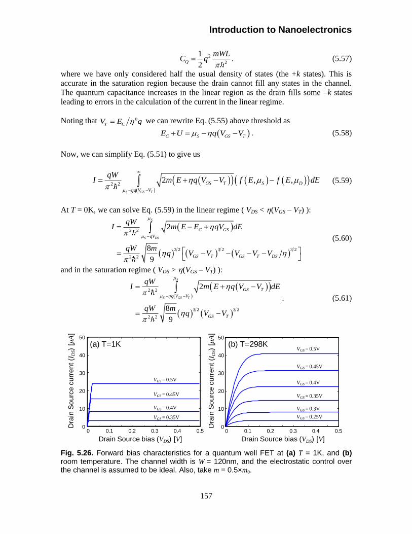
Introduction to Nanoelectronics
157
2
2
1
2Q
mWLC q
. (5.57)
where we have only considered half the usual density of states (the +k states). This is
accurate in the saturation region because the drain cannot fill any states in the channel.
The quantum capacitance increases in the linear region as the drain fills some –k states
leading to errors in the calculation of the current in the linear regime.
Noting that 0
T CV E q we can rewrite Eq. (5.55) above threshold as
C S GS TE U q V V . (5.58)
Now, we can simplify Eq. (5.51) to give us
2 22 , ,
S GS T
GS T S D
q V V
qWI m E q V V f E f E dE
(5.59)
At T = 0K, we can solve Eq. (5.59) in the linear regime ( VDS < (VGS – VT) ):
2 2
3 2 3 2 3 2
2 2
2
8
9
S
S DS
C GS
qV
GS T GS T DS
qWI m E E qV dE
qW mq V V V V V
(5.60)
and in the saturation regime ( VDS > (VGS – VT) ):
2 2
3 2 3 2
2 2
2
8
9
S
S GS T
GS T
q V V
GS T
qWI m E q V V dE
qW mq V V
. (5.61)
Fig. 5.26. Forward bias characteristics for a quantum well FET at (a) T = 1K, and (b) room temperature. The channel width is W = 120nm, and the electrostatic control over the channel is assumed to be ideal. Also, take m = 0.5×m0.
0 0.1 0.2 0.3 0.4 0.50
10
20
30
40
50
0 0.1 0.2 0.3 0.4 0.5
Drain Source bias (VDS) [V]
Dra
in S
ou
rce
cu
rre
nt
(ID
S)
[A
]
(a) T=1K
VGS = 0.5V
VGS = 0.45V
VGS = 0.4V
VGS = 0.35V
Drain Source bias (VDS) [V]
Dra
in S
ou
rce
cu
rre
nt
(ID
S)
[A
]
(b) T=298KVGS = 0.5V
VGS = 0.45V
VGS = 0.4V
VGS = 0.35V
VGS = 0.3V
0
10
20
30
40
50
VGS = 0.25V
Part 5. Field Effect Transistors
158
S DG
insulator
channel
contacts
silicon
Note that the saturation current goes as ~ (VGS-VT)3/2
compared to the ballistic nanowire
transistor, which goes as ~ (VGS-VT). As we shall see, the conventional FET has a
saturation current dependence of ~ (VGS-VT)2.
(iii) Conventional MOSFETs
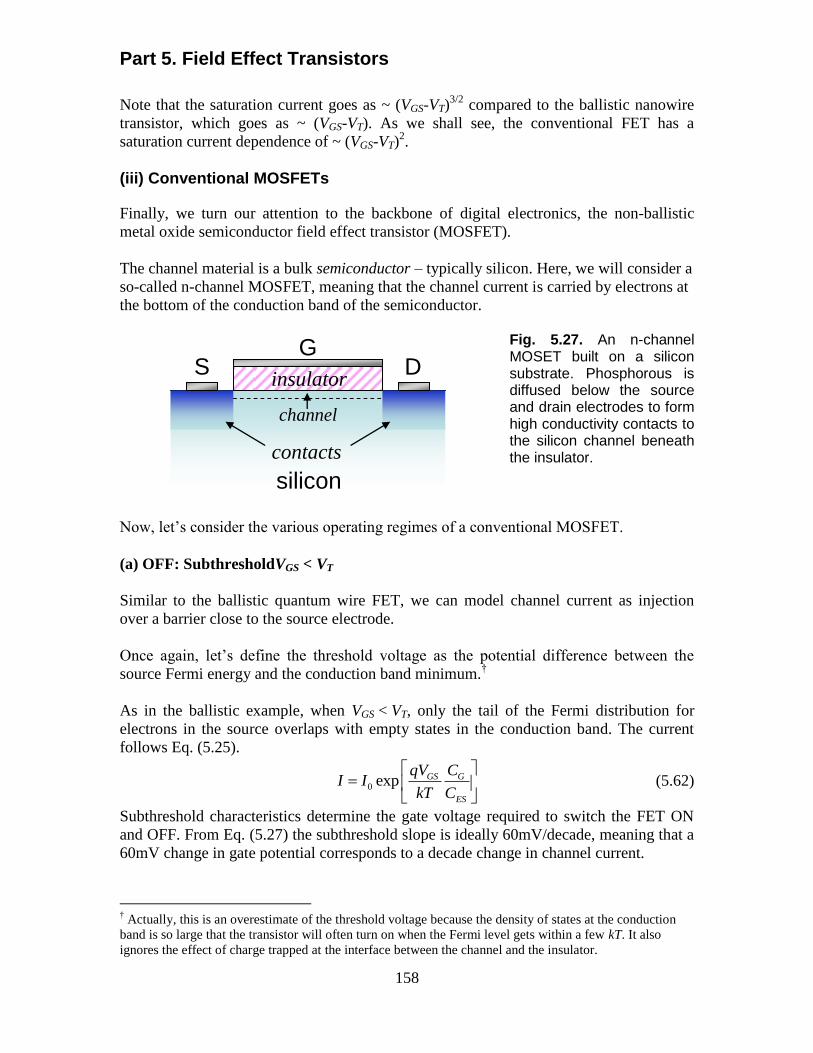
Finally, we turn our attention to the backbone of digital electronics, the non-ballistic
metal oxide semiconductor field effect transistor (MOSFET).
The channel material is a bulk semiconductor – typically silicon. Here, we will consider a
so-called n-channel MOSFET, meaning that the channel current is carried by electrons at
the bottom of the conduction band of the semiconductor. Fig. 5.27. An n-channel MOSET built on a silicon substrate. Phosphorous is diffused below the source and drain electrodes to form high conductivity contacts to the silicon channel beneath the insulator.
Now, let‟s consider the various operating regimes of a conventional MOSFET.
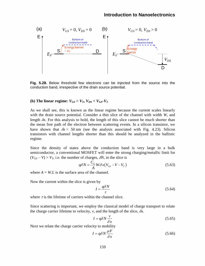
(a) OFF: SubthresholdVGS < VT
Similar to the ballistic quantum wire FET, we can model channel current as injection
over a barrier close to the source electrode.
Once again, let‟s define the threshold voltage as the potential difference between the
source Fermi energy and the conduction band minimum.†
As in the ballistic example, when VGS < VT, only the tail of the Fermi distribution for
electrons in the source overlaps with empty states in the conduction band. The current
follows Eq. (5.25).
0 exp GS G
ES
qV CI I
kT C
(5.62)
Subthreshold characteristics determine the gate voltage required to switch the FET ON
and OFF. From Eq. (5.27) the subthreshold slope is ideally 60mV/decade, meaning that a
60mV change in gate potential corresponds to a decade change in channel current.
† Actually, this is an overestimate of the threshold voltage because the density of states at the conduction
band is so large that the transistor will often turn on when the Fermi level gets within a few kT. It also
ignores the effect of charge trapped at the interface between the channel and the insulator.
Introduction to Nanoelectronics
159
Fig. 5.28. Below threshold few electrons can be injected from the source into the conduction band, irrespective of the drain source potential.
(b) The linear regime: VGS > VT, VDS < VGS-VT
As we shall see, this is known as the linear regime because the current scales linearly
with the drain source potential. Consider a thin slice of the channel with width W, and
length x. For this analysis to hold, the length of this slice cannot be much shorter than
the mean free path of the electron between scattering events. In a silicon transistor, we
have shown that x > 50 nm (see the analysis associated with Fig. 4.23). Silicon
transistors with channel lengths shorter than this should be analyzed in the ballistic
regime.
Since the density of states above the conduction band is very large in a bulk
semiconductor, a conventional MOSFET will enter the strong charging/metallic limit for
(VGS – V) > VT, i.e. the number of charges, N, in the slice is
GGS T
Cq N W x V V V
A (5.63)
where A = W.L is the surface area of the channel.
Now the current within the slice is given by
q N
I
(5.64)
where is the lifetime of carriers within the channel slice.
Since scattering is important, we employ the classical model of charge transport to relate
the charge carrier lifetime to velocity, v, and the length of the slice, x.
v
I q Nx
(5.65)
Next we relate the charge carrier velocity to mobility
F
I q Nx
(5.66)
S D
EBottom of
conduction band
(a)
EF
Energy barrier
~ VT
VDS
S
D
E
(b)
EF
Energy
barrier
VGS = 0, VDS = 0 VGS = 0, VDS > 0
Bottom of
conduction band
Part 5. Field Effect Transistors
160
Now, we must note that scattering causes the potential in the channel to vary with
position. We define the channel potential V(x) as a function of position in the channel.
Thus, expressing the source-drain electric field in terms of the channel potential we have
V
I q Nx x
(5.67)
Next, we substitute Eq. (5.63) into Eq. (5.67), yielding
GGS T
C VI V V V
L x
(5.68)
We solve this under the limit that x << L, by integrating both sides with respect to x.
Since the current is uniform throughout the channel, we obtain:
0
.
L
GGS T
C dVI L V V V dx
L dx (5.69)
where L is the length of the channel. It is convenient to change the variable of integration
on the righthand side to voltage. In the linear regime, the maximum channel potential is
VDS, hence:
2
0
DSV
GGS T
CI V V V dV
L (5.70)
The linear regime requires that the entire channel remains in the strong charging/metallic
limit. This occurs if the gate to drain potential, VGD, also exceeds VT
GD TV V (5.71)
or we can re-write this as
DS GS TV V V (5.72)
Under this constraint, Eq. (5.70) yields
2
2
1
2
GGS T DS DS
CI V V V V
L
(5.73)
It is standard to express this in terms of a gate capacitance per unit channel area, COX:
21
2OX GS T DS DS
WI C V V V V
L
(5.74)
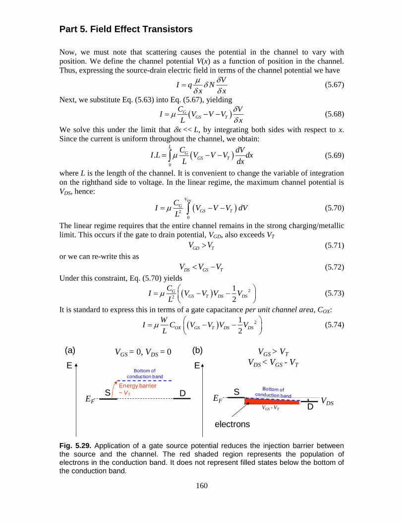
Fig. 5.29. Application of a gate source potential reduces the injection barrier between the source and the channel. The red shaded region represents the population of electrons in the conduction band. It does not represent filled states below the bottom of the conduction band.
SEF VDS
D
E
VGS > VT
VDS < VGS - VT
S D
EBottom of
conduction band
(a)
EF
Energy barrier
~ VT
VGS = 0, VDS = 0 (b)
electrons
VGS - VT

Introduction to Nanoelectronics
161
0 0.1 0.2 0.3 0.4 0.50
1
2
3
4
Drain Source bias (VDS) [V]
Dra
in S
ou
rce
cu
rre
nt
(ID
S)
[A
] T=298KVGS = 0.5V
VGS = 0.45V
VGS = 0.4V
VGS = 0.35V
(c) Saturation: VGS > VT, VDS > VGS-VT
If the gate to drain potential exceeds threshold then the channel region close to the drain
enters the zero charging regime, characterized by a high electric field and low density of
mobile charges. The channel is said to pinch off and the current saturates because it is no
longer dependent on VDS. The strong charging/metallic region ends when the local
channel potential V = VGS - VT
0
GS TV V
OX GS T
WI C V V V dV
L
(5.75)
which gives
2
2
OXGS T
CWI V V
L (5.76)
The IV characteristics of a non-ballistic MOSFET are shown in Fig. 5.31.
Fig. 5.30. As the drain-source potential increases, the channel near the drain enters the zero charging regime. The current is dependent only on the charge in the strong charging region, not on VDS. The red shaded region represents the population of
electrons in the conduction band. It does not represent filled states below the bottom of the conduction band.
Fig. 5.31. The IV characteristics of a non-ballistic MOSFET with
= 300 cm2/Vs, L = 40nm, W = 3 × L, VT = 0.3V, and CG = 0.1 fF. Note that the use
of the classical model for a transistor with such a short channel is inappropriate.
SS D
E
Bottom of
conduction bandEF EF
VDS
D
E
(b)VGS > VT
VDS = 0
VGS > VT
VDS > VGS - VT
(a)
electrons electrons
Pinch off
VGS - VT VGS - VT

Part 5. Field Effect Transistors
162
Comparison of ballistic and non-ballistic MOSFETs.
If we calculate the IV of a conventional MOSFET with a channel length in the ballistic
regime, we obtain IV curves that are qualitatively similar to the ballistic result. For
example, the classical model of a MOSFET with a channel length of 40 nm is shown in
Fig. 5.31. It is qualitatively similar to Fig. 5.26. Both possess a linear and a saturation
regime, and both exhibit identical subthreshold behavior. But the magnitude of the
current differs quite substantially. The ballistic device exhibits larger channel currents
due to the absence of scattering.
Another way to compare ballistic and non-ballistic MOSFETs is to return to the water
flow analogy.† As before, the source and drain are modeled by reservoirs. The channel
potential is modeled by a plunger. Gate-induced changes in the channel potential cause
the plunger to move up and down in the channel. The most important difference between
the ballistic and non-ballistic MOSFETs is the profile of the water in the channel. The
height of the water changes in the non-ballistic device, whereas water in the ballistic
channel does not relax to lower energies during its passage across the channel.
Fig. 5.32. The water flow analogy for the operation of ballistic and classical MOSFETs. Conduction in the channel is controlled by a plunger that models the channel potential. The transistors are turned ON by lowering the gate potential. Then, as the height of the drain reservoir decreases (corresponding to increased VDS), the channel first enters the linear regime (where current flow is limited by VDS) and then the saturation regime where the current is controlled only by the gate potential.
† For a more detailed treatment of the water analogy to conventional FETs see Tsividis, „Operation and
Modeling of the MOS transistor‟, 2nd
edition, Oxford University Press (1999).
source channel drain
VS VD
source channel drain
VS VD
source channel drain
VS VD
source channel drain
VS
VD
OFF
ON
LINEAR
SAT
BALLISTIC
source channel drain
VS VD
source channel drain
VS VD
source channel drain
VS VD
source channel drain
VS
VD
CLASSICAL
Introduction to Nanoelectronics
163
Problems
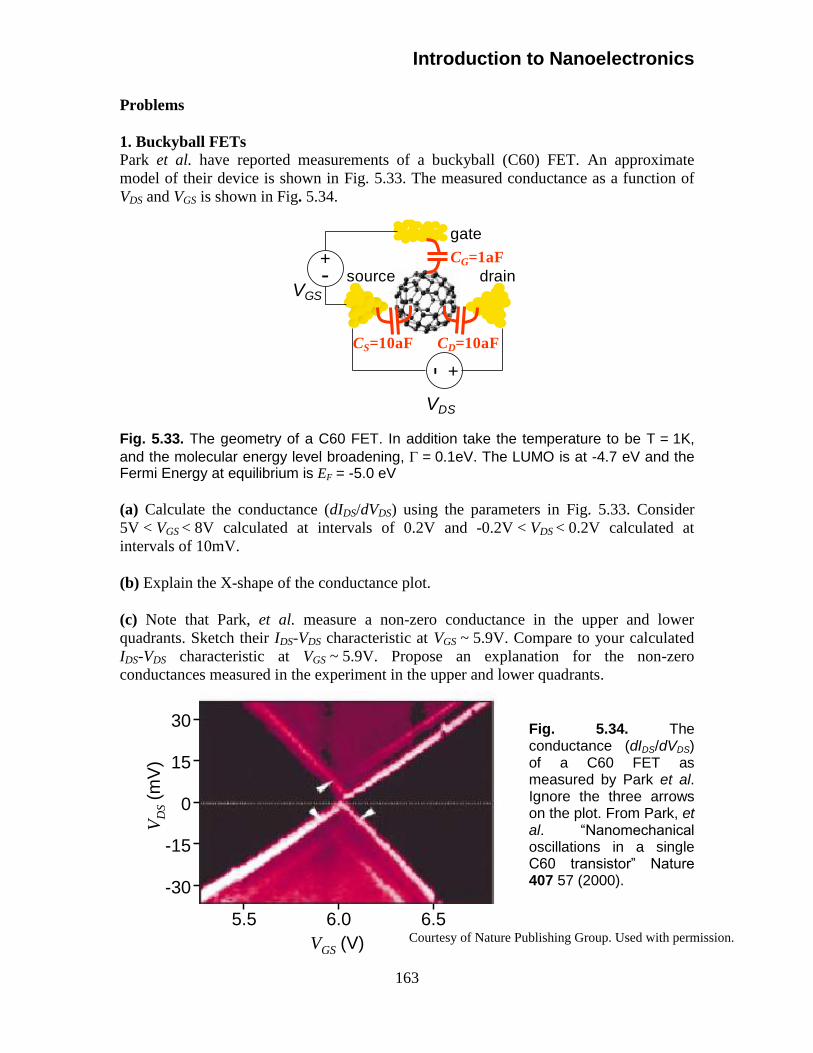
1. Buckyball FETs
Park et al. have reported measurements of a buckyball (C60) FET. An approximate
model of their device is shown in Fig. 5.33. The measured conductance as a function of
VDS and VGS is shown in Fig. 5.34.
Fig. 5.33. The geometry of a C60 FET. In addition take the temperature to be T = 1K,
and the molecular energy level broadening, G = 0.1eV. The LUMO is at -4.7 eV and the Fermi Energy at equilibrium is EF = -5.0 eV
(a) Calculate the conductance (dIDS/dVDS) using the parameters in Fig. 5.33. Consider
5V < VGS < 8V calculated at intervals of 0.2V and -0.2V < VDS < 0.2V calculated at
intervals of 10mV.
(b) Explain the X-shape of the conductance plot.
(c) Note that Park, et al. measure a non-zero conductance in the upper and lower
quadrants. Sketch their IDS-VDS characteristic at VGS ~ 5.9V. Compare to your calculated
IDS-VDS characteristic at VGS ~ 5.9V. Propose an explanation for the non-zero
conductances measured in the experiment in the upper and lower quadrants.
Fig. 5.34. The conductance (dIDS/dVDS) of a C60 FET as measured by Park et al. Ignore the three arrows on the plot. From Park, et al. “Nanomechanical oscillations in a single C60 transistor” Nature 407 57 (2000).
5.5 6.0 6.5
15
0
-15
-30
30
VGS (V)
VD
S(m
V)
+-VDS
source drain+-
VGS
gate
CG=1aF
CS=10aF CD=10aF
Courtesy of Nature Publishing Group. Used with permission.
Part 5. Field Effect Transistors
164
(d) In Park et al.‟s measurement the conductance gap vanishes at VGS = 6.0V. Assuming
that CG is incorrect in Fig. 5.33, calculate the correct value.
Reference
Park, et al. “Nanomechanical oscillations in a single C60 transistor” Nature 407 57
(2000)
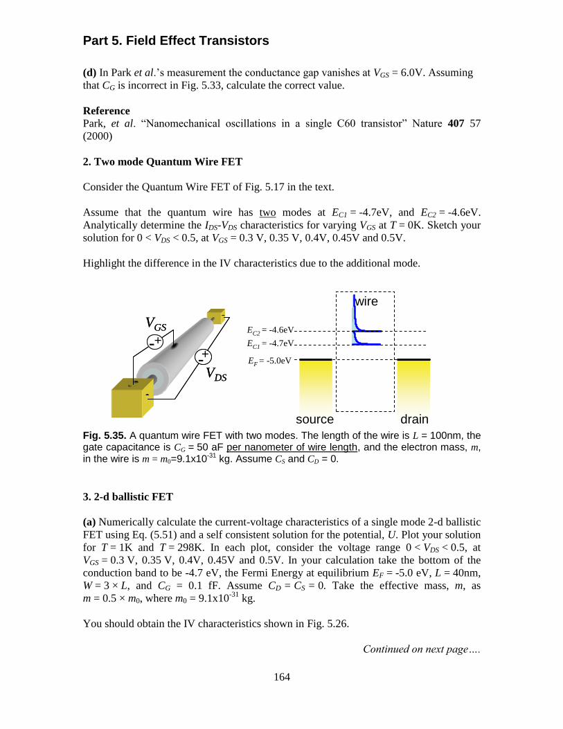
2. Two mode Quantum Wire FET
Consider the Quantum Wire FET of Fig. 5.17 in the text.
Assume that the quantum wire has two modes at EC1 = -4.7eV, and EC2 = -4.6eV.
Analytically determine the IDS-VDS characteristics for varying VGS at T = 0K. Sketch your
solution for 0 < VDS < 0.5, at VGS = 0.3 V, 0.35 V, 0.4V, 0.45V and 0.5V.
Highlight the difference in the IV characteristics due to the additional mode.
Fig. 5.35. A quantum wire FET with two modes. The length of the wire is L = 100nm, the gate capacitance is CG = 50 aF per nanometer of wire length, and the electron mass, m, in the wire is m = m0=9.1x10⁻³¹ kg. Assume CS and CD = 0.
3. 2-d ballistic FET
(a) Numerically calculate the current-voltage characteristics of a single mode 2-d ballistic
FET using Eq. (5.51) and a self consistent solution for the potential, U. Plot your solution
for T = 1K and T = 298K. In each plot, consider the voltage range 0 < VDS < 0.5, at
VGS = 0.3 V, 0.35 V, 0.4V, 0.45V and 0.5V. In your calculation take the bottom of the
conduction band to be -4.7 eV, the Fermi Energy at equilibrium EF = -5.0 eV, L = 40nm,
W = 3 × L, and CG = 0.1 fF. Assume CD = CS = 0. Take the effective mass, m, as
m = 0.5 × m0, where m0 = 9.1x10⁻³¹
kg.
You should obtain the IV characteristics shown in Fig. 5.26.
Continued on next page….
wire
EF = -5.0eV
EC1 = -4.7eV
source drain
EC2 = -4.6eV
+-VDS
VGS+-+-
VDS
VGS+-
Introduction to Nanoelectronics
165
(b) Next, compare your numerical solutions to the analytic solution for the linear and
saturation regions (Eqns (5.60) and (5.61)). Explain the discrepancies.
(c) Numerically determine IDS vs VGS at VDS = 0.5V and T = 298K. Plot the current on a
logarithmic scale to demonstrate that the transconductance is 60mV/decade in the
subthreshold region.
(d) Using your plot in (c), choose a new VT such that the analytic solution for the
saturation region (Eq. (5.61)) provides a better fit at room temperature. Explain your
choice.
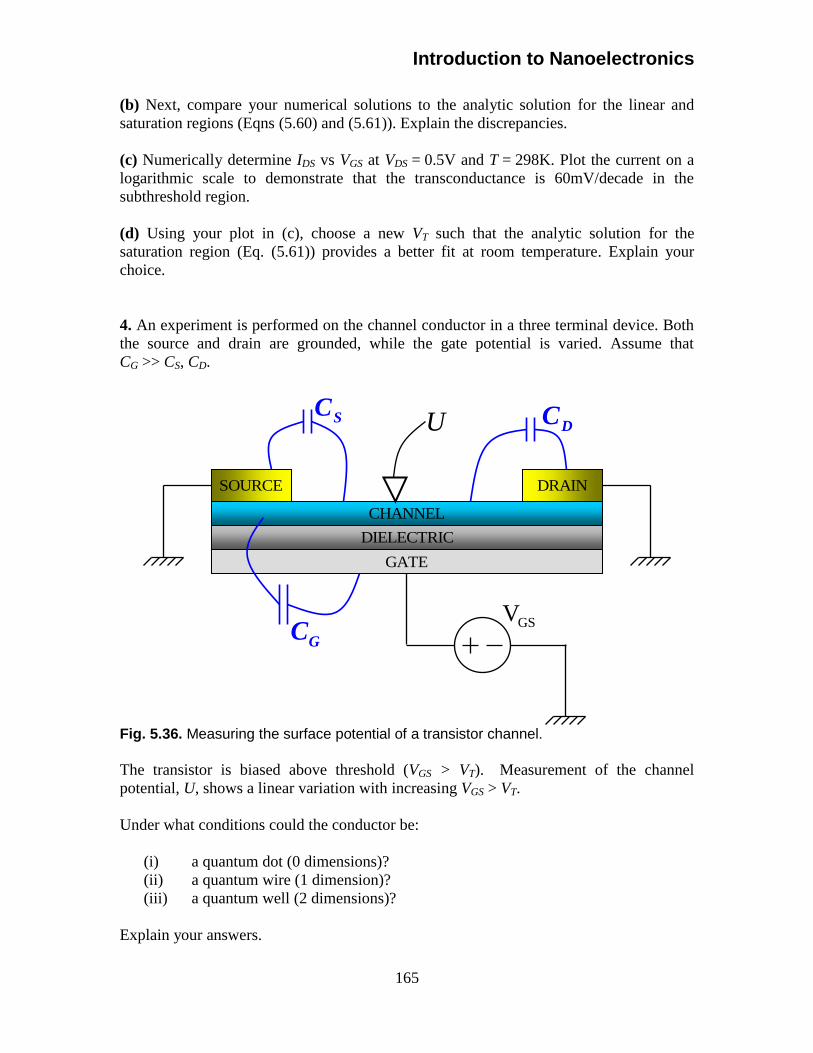
4. An experiment is performed on the channel conductor in a three terminal device. Both
the source and drain are grounded, while the gate potential is varied. Assume that
CG >> CS, CD.
Fig. 5.36. Measuring the surface potential of a transistor channel.
The transistor is biased above threshold (VGS > VT). Measurement of the channel
potential, U, shows a linear variation with increasing VGS > VT.
Under what conditions could the conductor be:
(i) a quantum dot (0 dimensions)?
(ii) a quantum wire (1 dimension)?
(iii) a quantum well (2 dimensions)?
Explain your answers.
GATE
CHANNEL
DIELECTRIC
SOURCE DRAIN
GSV
U
GC
DCSC
Part 5. Field Effect Transistors
166
1 2
D
SOURCE DRAIN
GSV
DSV
1 2
D
SOURCE DRAIN
GSV
DSV
1 2 D
SOURCE DRAIN
GS V
DS V
1 2 D
SOURCE DRAIN
GS V
DS V
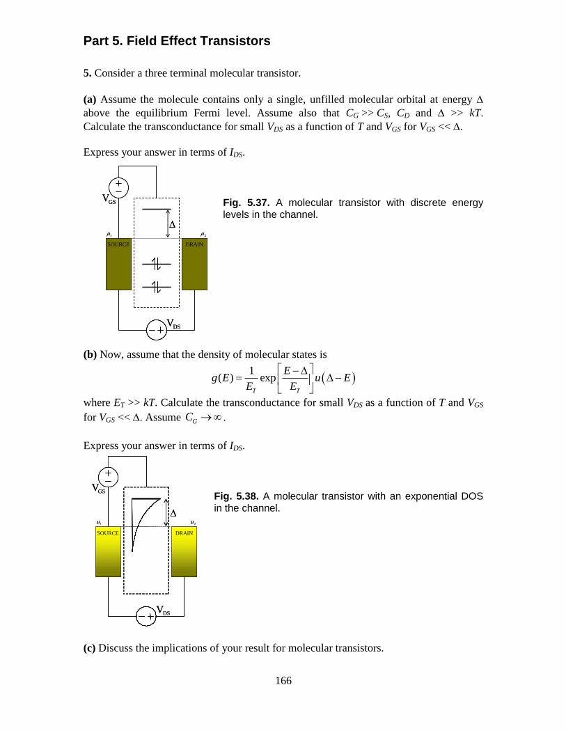
5. Consider a three terminal molecular transistor.
(a) Assume the molecule contains only a single, unfilled molecular orbital at energy D
above the equilibrium Fermi level. Assume also that CG >> CS, CD and D >> kT.
Calculate the transconductance for small VDS as a function of T and VGS for VGS << D.
Express your answer in terms of IDS.
Fig. 5.37. A molecular transistor with discrete energy levels in the channel.
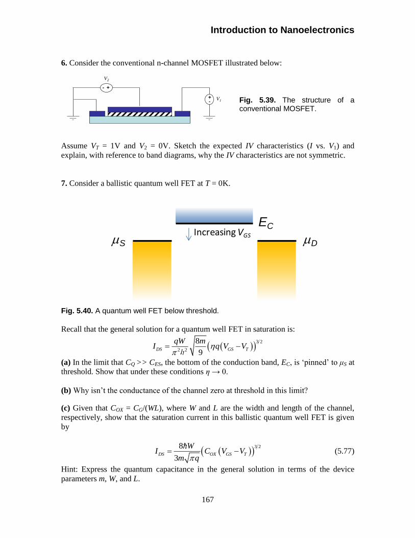
(b) Now, assume that the density of molecular states is
1
( ) expT T
Eg E u E
E E
D D
where ET >> kT. Calculate the transconductance for small VDS as a function of T and VGS
for VGS << D. Assume GC .
Express your answer in terms of IDS.
Fig. 5.38. A molecular transistor with an exponential DOS in the channel.
(c) Discuss the implications of your result for molecular transistors.
Introduction to Nanoelectronics
167
- +
V2
V1+-
6. Consider the conventional n-channel MOSFET illustrated below:
Fig. 5.39. The structure of a conventional MOSFET.
Assume VT = 1V and V2 = 0V. Sketch the expected IV characteristics (I vs. V1) and
explain, with reference to band diagrams, why the IV characteristics are not symmetric.
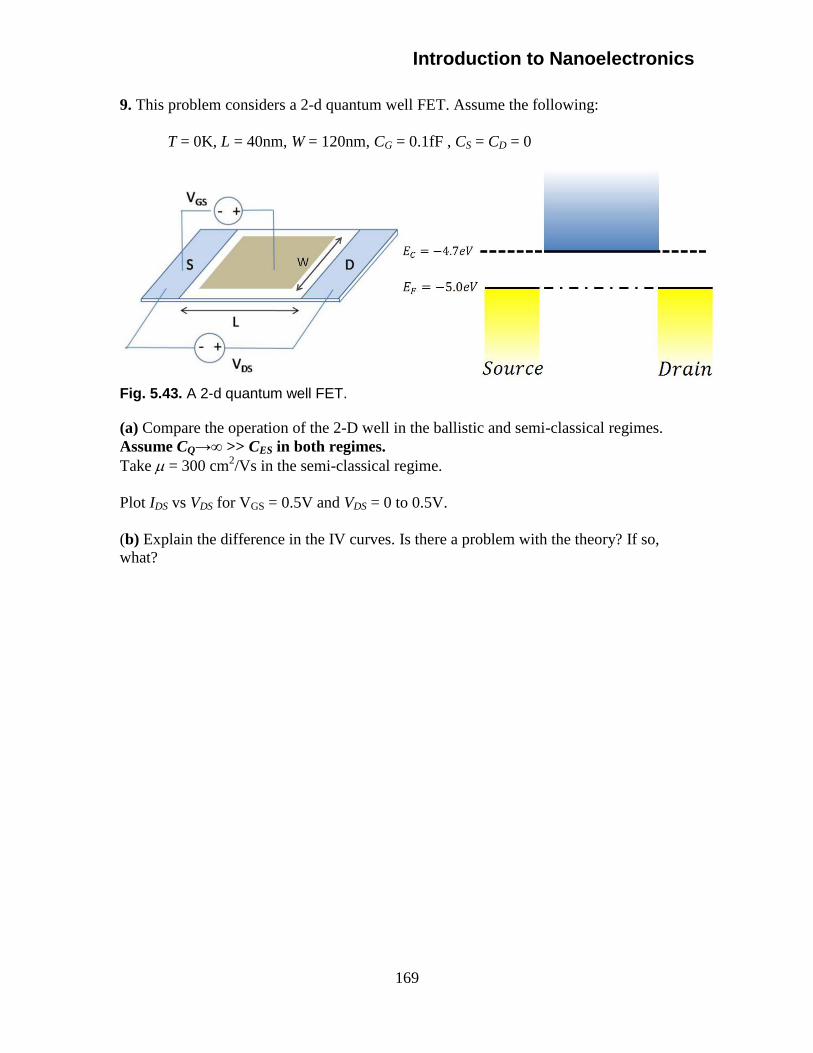
7. Consider a ballistic quantum well FET at T = 0K.
Fig. 5.40. A quantum well FET below threshold.
Recall that the general solution for a quantum well FET in saturation is:
3 2
2 2
8
9DS GS T
qW mI q V V
(a) In the limit that CQ >> CES, the bottom of the conduction band, EC, is „pinned‟ to μS at
threshold. Show that under these conditions η → 0.
(b) Why isn‟t the conductance of the channel zero at threshold in this limit?
(c) Given that COX = CG/(WL), where W and L are the width and length of the channel,
respectively, show that the saturation current in this ballistic quantum well FET is given
by
3 28
3DS OX GS T
WI C V V
m q (5.77)
Hint: Express the quantum capacitance in the general solution in terms of the device
parameters m, W, and L.
S D
ECIncreasing VGS
S D
ECIncreasing VGS

Part 5. Field Effect Transistors
168
8. A quantum well is connected to source and drain contacts. Assume identical source
and drain contacts.
Fig. 5.41. A quantum well with source and drain contacts.
(a) Plot the potential profile along the well when VDS = +0.3V.
Now a gate electrode is positioned above the well. Assume that , except very
close to the source and drain electrodes. At the gate electrode ε = 4×8.84×10-12
F/m and
d = 10nm. Assume the source and drain contacts are identical.
Fig. 5.42. The quantum well with a gate electrode also.
(b) What is the potential profile when VDS = 0.3V and VGS = 0V.
(c) Repeat (b) for VDS = 0V and VGS = 0.7V. Hint: Check the CQ.
(d) Repeat (b) for VDS = 0.3V and VGS = 0.7V assuming ballistic transport.
(e) Repeat (b) for VDS = 0.3V and VGS = 0.7V assuming non-ballistic transport.
Introduction to Nanoelectronics
169
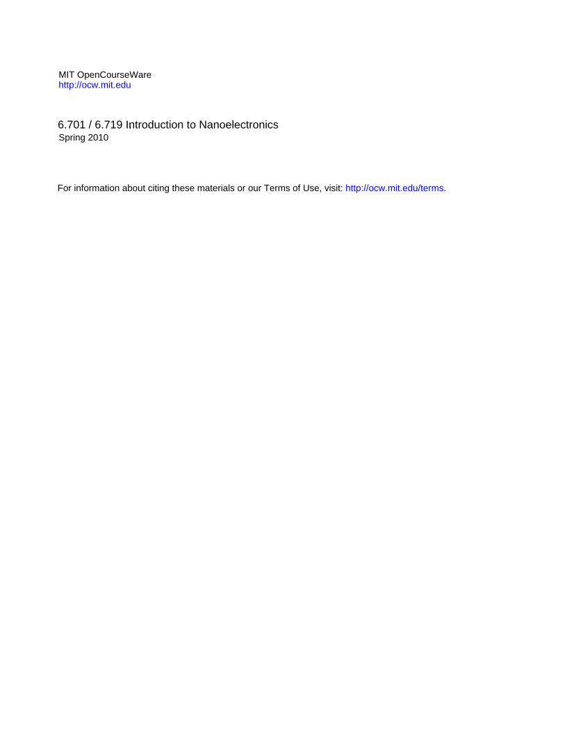
9. This problem considers a 2-d quantum well FET. Assume the following:
T = 0K, L = 40nm, W = 120nm, CG = 0.1fF , CS = CD = 0
Fig. 5.43. A 2-d quantum well FET.
(a) Compare the operation of the 2-D well in the ballistic and semi-classical regimes.
Assume CQ→∞ >> CES in both regimes.
Take = 300 cm2/Vs in the semi-classical regime.
Plot IDS vs VDS for VGS = 0.5V and VDS = 0 to 0.5V.
(b) Explain the difference in the IV curves. Is there a problem with the theory? If so,
what?
MIT OpenCourseWare http://ocw.mit.edu
6.701 / 6.719 . Introduction to Nanoelectronics�� Spring 2010
For information about citing these materials or our Terms of Use, visit: http://ocw.mit.edu/terms.