
Part 1 : Flow of IC Design - pudn.comread.pudn.com/.../sourcecode/embed/84546/IC_design_flow.pdf ·...
43
Flow of IC Design 1 Beihang University College of Software Graduate School of Integrated Circuits Design Summer Course Aug. 30 – Sep. 5, 2004 Part 1 : Flow of IC Design James Yang if (trn_data_period) begin // send normal data trn_crc_data <= trn_data[7:4]; // the 1st nibble ext_trn <= 1; end else begin // send SCR, SD status, etc trn_crc_data <= ssw_data[7:4]; // the 1st nibble ext_ssw <= 1; end
Transcript of Part 1 : Flow of IC Design - pudn.comread.pudn.com/.../sourcecode/embed/84546/IC_design_flow.pdf ·...

Flow of IC Design
1
Beihang University College of Software
Graduate School of Integrated Circuits Design Summer Course
Aug. 30 – Sep. 5, 2004
Part 1 : Flow of IC Design
James Yang
if (trn_data_period) begin // send normal data trn_crc_data <= trn_data[7:4]; // the 1st nibble ext_trn <= 1; end else begin // send SCR, SD status, etc trn_crc_data <= ssw_data[7:4]; // the 1st nibble ext_ssw <= 1; end

Flow of IC Design
2
The schedule of 7-day course
Aug. 30 Aug. 31 Sep. 1 Sep. 2 Sep. 3 Sep. 4 Sep. 5
8:30 – 10:00
Part I 1-2
Part 2 19-27
Part 2 36-45
Part I 8-10 Part I
16-20 DFT (if we
have time)
10:00 – 10:30
Break + Q & A
Break + Q & A
Break + Q & A
Break + Q & A Break +
Q & A Break + Q & A
10:30 – 12:00
Part I 3-5
Part 2 28-35
Part I 6-7
Part I 11-15 Part I
20-26 DFT (if we
have time)
12:00 – 13:00 lunch lunch lunch lunch lunch lunch
13:00 – 14:30
Part 2 1-10
Part III Lab
Part III Lab
Part III Lab
Part III Lab
Part III Lab
Part III Lab
14:30 15:00
Break + Q & A
Design coding
Test bench coding
RTL sim.
FPGA syn. & routing
FPGA verify.
FPGA verify.
15:30 – 17:00
Part 2 11-18
After 17:00
Break + Q & A
1. Assume James Yang will go to conference in the morning of Sept. 3 2. There are 26 topics in part 1. 3. There are 45 topics in Part 2 4. The schedule is flexible, depending on the students’ response. If we have time on the last day, we can study something about Design for Testability (DFT) The information collected in this topic is based on James Yang’s own working experience. The students can use the information as a reference. For some other cases such as more advanced projects, these information and suggestion may not be totally applicable.

Flow of IC Design
3
1. The Flow of IC Design
1. Product specification
2. Information collection/study
4. Architecture planning
5. Design : HDL source coding
7. RTL simulation/debug
3. IP preparation
8. FPGA netlist generation
10. FPGA verification/debug
9. Test environment setup
11. Netlist synthesis
12. Pre-sim SDF generation
6. HDL test bench coding
13. Pre-simulation
: IC designers’ jobs
: with more details inPart 2 and Part 3

Flow of IC Design
4
14. Layout guide writing
15. Chip layout
16. SPF generation
17. Post-sim SDF generation
18. Post-simulation 5.
19. LVS check
20.Tape-out
22. Test pattern generation 21. fabrication
23. Chip probe for wafer
24. Packaging & final testing
25. Real environment testing
26. Sales promotion

Flow of IC Design
5
2. Information Collection and Study There are many different fields in IC industry. The IC designers’ specialties also vary a lot. A good IC designer in Area A may take a long time to be familiar with the knowledge in Area B. In the beginning of our career life, we need to ask ourselves that what kind of IC designer we want to be ? Consumer electronics ? PC peripherals ? Communication ? Microprocessor or DSP ? …. ? The basic rules and flows of IC design are the same, no matter which kinds of products we are going to join. HDL, FPGA and EDA software, etc. are only the tools to help us in chip realization. The spirit of the IC is the knowledge. So the first challenge we will encounter is to obtain the related information for the design, then understand the information and implement it. Some information is not free, we need to join the association or buy the documents from their organizations such as ISO or IEEE, etc. The designers should also have strong background so they can understand them quickly, even improve the existing standards or algorithms. Therefore, in addition to polishing our design skill and tool manipulation, the good designers must have sufficient knowledge in their area, and keep on accumulating them. Ex. 1: 8-port Ethernet switching hub controller Knowledge : IEEE 802.3 standards including 10MHz Ethernet and 100MHz Fast Ethernet. Related area : Asynchronous Transfer Mode (ATM), IEEE 802.11 wireless LAN, IEEE 1394, USB, etc. Ex. 2 : Card reader + Image displayer Knowledge : Joint Picture Expert Group (JPEG) standards. Image format (RGB, YCbCr , CIF, QCIF, 422, 420, NTSC, PAL, etc.) Memory card specification (CF, SM, MMC, SD, MS,XD) File format Related area : Motion Picture Expert Group (MPEG) -1, MPEG-2, MPEG-4, MP3, etc. Ex. 3 : Secure Digital (SD) card controller Knowledge: SD card specification Flash memory (a non-volatile memory) specification Decryption algorithm and flow for SD card File format Related are : digital memory cards, thumb drive, non-volatile memory based devices, etc.
Idea, Standard, Specification, Algorithm, Architecture
HDL,FPGA, Simulation tools Cell library & synthesis tools Layout tools, etc.
Fabrication
Flow of IC Design
6
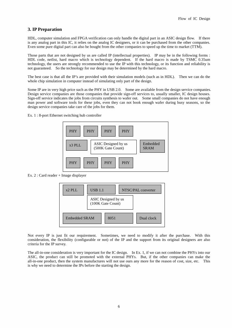
3. IP Preparation HDL, computer simulation and FPGA verification can only handle the digital part in an ASIC design flow. If there is any analog part in this IC, it relies on the analog IC designers, or it can be purchased from the other companies. Even some pure digital part can also be bought from the other companies to speed up the time to market (TTM). Those parts that are not designed by us are called IP (intellectual properties). IP may be in the following forms : HDL code, netlist, hard macro which is technology dependent. If the hard macro is made by TSMC 0.35um technology, the users are strongly recommended to use the IP with this technology, or its function and reliability is not guaranteed. So the technology for our design may be determined by the hard macro. The best case is that all the IP’s are provided with their simulation models (such as in HDL). Then we can do the whole chip simulation in computer instead of simulating only part of the design. Some IP are in very high price such as the PHY in USB 2.0. Some are available from the design service companies. Design service companies are those companies that provide sign-off services to, usually smaller, IC design houses. Sign-off service indicates the jobs from circuits synthesis to wafer out. Some small companies do not have enough man power and software tools for these jobs, even they can not book enough wafer during busy seasons, so the design service companies take care of the jobs for them. Ex. 1 : 8-port Ethernet switching hub controller Ex. 2 : Card reader + Image displayer Not every IP is just fit our requirement. Sometimes, we need to modify it after the purchase. With this consideration, the flexibility (configurable or not) of the IP and the support from its original designers are also criteria for the IP survey. The all-in-one consideration is very important for the IC design. In Ex. 1, if we can not combine the PHYs into our ASIC, the product can still be promoted with the external PHYs. But, if the other companies can make the all-in-one product, then the system manufactures will not use ours any more for the reason of cost, size, etc. This is why we need to determine the IPs before the starting the design.
PHY
Embedded SRAM
x3 PLL ASIC Designed by us(500K Gate Count)
x2 PLL
Embedded SRAM
NTSC/PAL converterUSB 1.1
Dual clock 8051
PHY PHYPHY
PHY PHY PHYPHY
ASIC Designed by us(100K Gate Count)

Flow of IC Design
7
4. Architecture Planning In the beginning, the designers must understand all the related specifications, standards and algorithms. But there are many ways to implement these specifications and algorithms. The best architecture is the one with the fastest speed and minimum chip size. Unfortunately, the requirement of fast speed is usually contradictory to the requirement of small die size. So, planning an optimal structure with certain trade-off is also an important issue before the job of HDL coding. Three common examples are given below. They are the adder, the divider and the motion estimator in MPEG.. Ex. 1: The adder Normal 4-bit Adder : A[3:0] + B[3:0] = S[4:0], one stage by one stage Look-ahead Adder : expects the carry earlier. It has more gate count, but much faster. Ex. 2 : The divider The divisor is fixed. The fastest way is look-up table for this function. But this method needs large memory. We can subtract the divisor from the dividend repeatedly until the new dividend is less than the divisor. It may take long time but with minimum hardware efforts. There are still many ways to implement the divider. Each has its own advantages and drawbacks. Ex. 3 : Motion Estimator : Find the most similar 8x8 block from the previous picture in one movie.
Basically, there are full search method and three-step search method. Many papers have discussed the architecture to optimize the hardware complexity and speed. The following two examples are our real cases that the architectures are emphasized. Ex. 1 : Card reader + Image displayer Ex. 2 : Secure Digital (SD) card controller 8051 is not fast enough to handle the fast response required by SD card, so many work are share by hardware. The negotiation between hardware and firmware engineers is very important.
A0B0 C0A1B1 C1A2B2 C2A3B3
S0 S1 S2 S3 S4
Variable length decoder (by Prof. Chen)
De- Quantization & ZigZag Scan
Inverse Discrete Cosine Transform (by one paper)
Zoom (by one paper)
To
NTSC TV

Flow of IC Design
8
* Jan Ti Yang & S.Z. Hsieh, etc. “Optimized Structure for Fast Data Storage to Non-Volatile Memory with Minimum Chip Size”, ICSP’04, Beijing, Aug. 2004. * Jan Ti Yang & S.Z. Hsieh, etc.“ Performance Comparison of Logical Address to Physical Address Algorithms for Non-Volatile Memory”, ASICON’2003, Beijing, Oct. 2003.
SD interface
Data buffer controlled by 8051 with hardware speed-up
Flash interface by special architecture*
FlashDigital
camera

Flow of IC Design
9
5. Design : HDL Source Coding A good designer is trained by practical experience and continuous study. We need to be very careful and patient in every design. Because one NRE (explained later) will costs a lot of money and several weeks, the designer will take the responsibility for the money and schedule loss if he/she did some careless mistakes. Experience and carefulness may be the best way to achieve a successful design. HDL is different from computer language such as C. In HDL, every statement is one circuit. All the statements work at the same time, no matter their order in the code. Compare the difference : In VHDL In C C <= A+ B; C = A+ B; D <= C + B; D = C + B; Assume A=5, B=6 and C=7 initially. In VHDL, C=11 and D=13 because both addition are executed in the same time. In C, C=11 but D=11+6=17 because the second statement is executed after the first one is done. Many students asked : should we learn VHDL at first, or verilog at first ? The answer will be given later. The following items are some suggestions for a stable and successful design : Naming style : 1. Don’t use the keywords as signal names 2. Don’t use the Verilog keyword as the signal names in VHDL because the final netlist is in Verilog. 3. Name the signal with meaning, use x or n as the first letter when this signal is active low. 4. Name the I/O pins as short as possible. 5. Don’t name the signal with upper and lower cases mixed. 6. It is the rule that the first letter of a signal name must be a – z. 7. make the module name, instance name and file name the same. Coding style : remember that a good code is a code that other people can read and understand easily. 1. Add comments as more as possible. Record the modification history. 2. Coding format is fixed and united for all the modules in one design. Follow the format that the project leader
assigns. 3. Divide the entire design into different module/entity of suitable number. 4. All the signals in one always/process must be related. 5. Don’t use the keywords or syntax those are used not often in order for safe synthesis. In the view point of
logic, all the logic circuits can be expressed by IF – THEN – ELSE. 6. Don’t use “deep” logic. 7. All the conditions in one IF must be related. Design style : 1. It is strongly recommended to do the synchronous design. 2. Always keep the timing issue in mind when doing design. The RTL simulation results may be the same as we
thought, but the practical results may be different. Ex. OR two consecutive pulses may not be equal to a two-clock pulse.
3. Determine the low or high reset, synch. or asynch. reset. reset, rising or falling edge trigger in the beginning of the design, and all the modules follow the decision.
4. Use IF and CASE in different situations. 5. Be careful in latching a signal or bus that is generated by the different clock. 6. Make sure that all the signals are reset. FPGA does reset automatically in power-up which may mislead the
designer as if they did it. 7. Never read any internal memory (ex. SRAM) before write it. FPGA makes all the bits in the internal SRAM
into 0’s in power-up. 8. Use data buffer when transfer data from one clock to a different clock, which works as the dual clock FIFO. 9. In VHDL, the 2-dimensional array is allowed, it is very useful. In Verilog, it is allowed in the test bench for
simulation only, it can not be synthesized. 10. Follow the register-in register-out rule. 11. Synthesis tool such as Synopsys DesignCompiler, is very stable, any bugs must come from the design code, can
not be from synthesis tools. 12. Make the FPGA version and ASIC version as similar as possible, especially the SRAM types. It is ideal that
the two versions are the same. 13. Make build-in-self-test (BIST) circuits for embedded memory. 14. Dummy cells and some other remedy circuits are necessary. 15. Some simple test circuits are needed. Usually there are several test modes in one chip.

Flow of IC Design
10
16. Do gating clock when idle to save power. 17. Don’t rely on the script to guarantee the design (Ex. Synopsys full_case). But some good constraint in script
can do the better performance (Ex. Look-ahead adder). 18. If time is sufficient, do one more latch by clock instead of using MUX. 19. Don’t use internal tri-state. FPGA may not have such circuits. ASIC requires bus holder to handle internal
tri-state. 20. Do the pad insertion on the top level. So the output enable signal of every bi-directional pad will be taken out to
the top level. 21. Be very careful in selecting pad. (Ex. pull up ability, Schmitt trigger, 5V tolerant, clock pads, etc.) 22. Be aware of the problem caused by clock skew. 23. Don’t try to generate the half-cycle signal. 24. If there are many functions to be revised, do it one by one, i.e., revise one function and check one function. 25. It is a good habit to align the bit number of every signal in one computation equation, even though the synthesis
tool can handle it. 26. Never use division provided by HDL. 27. Reduce the unnecessary clock. It causes trouble in design and layout. Most of the FPGA has 1-4 dedicate
clock paths only.

Flow of IC Design
11
6. HDL Test Bench Coding Test bench is also the HDL code that provides the simulation models for the devices connected with the ASIC. The efforts in designing test bench may not be less than that in designing ASIC. For the ASIC with many peripheral devices, it may take much longer time in coding the test bench than coding the ASIC. Ex. : Secure Digital (SD) card controller The following items are some requirements for a good test bench Even though the test bench is not for synthesis and can be coded in a easier way, but we should notice the following items : 1. The test bench can cover as more cases as possible, both the function cases and timing cases. So it is
recommended that the designers for test bench are different from the designers for the ASIC. 2. The test bench must be flexible. New testing condition can be added easily. 3. Log the test results for automatic comparison instead of checking the results by eyes. 4. All the results of IC pins are logged as the pattern for the IC testers. 5. If there are some functions that FPGA verification can not afford, the test bench must cover them. 6. Try to make the test bench as close to the real environment as possible (Ex. external memory). 7. It is better to make an integrated test bench. A test bench with too many separate modules is not easy to be
maintained. A typical test bench contains the following items :
ASIC part
8051 + firmware
Flash model provided by Samsung
Some other models such as embedded OSC, POR
Host (card reader) model
Declaration for dump file and signals
External signal (reset, clock) generation
Wire declaration for ASIC/sim-models interconnection
Declaration for ASIC/sim-models
Input/output log

Flow of IC Design
12
7. RTL Simulation/Debug RTL simulation is also called the behavioral simulation or functional simulation. It is only based on the register transfer level (RTL) function, timing is not considered. The delay in the stage is called the delta delay, it really exist but can not be shown on the waveform. Ex : Delta delay is effective only for the signals generated by the same clock. If the signal is latched by the other clock, both clocks have the same frequency and phase, then unknown condition may happen. So we need to insert a little delay in this situation. All the design must pass the RTL simulation with fair test bench at first, then the source code can be synthesized into netlist for FPGA or pre-sim. If not, the debug work on FPGA will be terrible. The most popular simulation tool is the Cadence Verilog-XL. It is recognized by all the companies that Verilog-XL is the standard to check the simulation results. But it is the workstation version. For the PC version, ModelSim is a good choice. The simulation results are close to those of Verilog-XL. There are many tools can be used to see the waveform. Debussy is very popular because of it small size of dump file. The goal of simulation is to find out the errors before hardware realization. So it takes many iterations to modify the code and do re-simulation until there is no bugs (at least can not be found with the test bench). Then, the results (waveform) will be checked very carefully, some important outputs are logged as the “golden pattern”. From now on, we can compare the output directly to see if the results are correct. Some functions are very difficult to be tested. To test them requires long pattern. We need to think how to overcome this problem, some circuits may be added to achieve this goal. Ex . Secure Digital (SD) card controller There are almost 800K cycles in the test pattern, but toggle rate is about 70%. An example of the waveform from RTL simulation is shown below :
D Q
CLK
D_IN Q_OUT
CLK
D_IN
Q OUT
Delta Delay -> 0

Flow of IC Design
13
8. FPGA Netlist Generation The restriction of FPGA : here the Altera FPGA’s are used as the example. 1. Every FPGA has its own capacity limitation. We can not download our design into an FPGA with 90% utility
rate or even higher. Take Altera 20K200 as the example, 50K gate count will takes more then 80% utility. It may restrict the performance of the FPGA. So we use Altera 20K600, it takes 30% only.
2. There are only 2 clock paths for clock and 4 dedicate input for reset, etc. If there are more clocks, it may be a trouble. Any clock generated inside the design is suggested to be routed out of the FPGA, the goes into FPGA again through the clock path.
3. There are embedded memory inside the FPGA. If the design contains large embedded SRAM, the FPGA may not have so much. So we need to added external memory outside the FPGA. Also, the memory types may be different from the real embedded ones.
4. Altera’s FPGA will reset all the register outputs and SRAM data into 0 at power up, no matter we do it or not. It may be dangerous for the final chip because the FPGA works find and, actually, we did not do the reset in our design.
5. Some FPGA’s declare its high speed. These information are based on some special cases. With high utility, the stable speed will not be over 50MHz usually. For some design with high speed and large gate count (Ex. : 8-port Ethernet switching hub controller : the clock is 75MHz, the gate count is 500K), FPGA verification is not practical. Otherwise, the design is separated into several FPGAs and verified with lower clock rate.
After RTL-simulation, our design code can be synthesized into the FPGA netlist. The synthesis tool used here is the Synopsys FPGA Express of PC version. The synthesized netlist is the EDIF file, not the verilog file. The following example is one paragraph of the edif netlist, not easy to be read. edif all_top (edifVersion 2 0 0) (edifLevel 0) (keywordMap (keywordLevel 0) ) (status (written (timeStamp 2004 3 30 8 54 19) (program "FPGA Compiler II" (version "3.5.1.6112") ) (author "RD") ) ) (external UnlinkedDesignLibrary (edifLevel 0) (technology (numberDefinition) ) (cell syn_ram_512x8_irou (cellType GENERIC) (view Netlist_representation (viewType NETLIST) (interface (port (array (rename Q_7_0 "Q[7:0]") 8 ) (direction OUTPUT) ) (port (array (rename Data_7_0 "Data[7:0]") 8 ) (direction INPUT) ) (port WE (direction INPUT) ) (port (array (rename Address_8_0 "Address[8:0]") 9

Flow of IC Design
14
) (direction INPUT) ) (port Inclock (direction INPUT) ) ) ) ) ……………………………………
(instance buf26_reg0 (viewRef Netlist_representation (cellRef APEX20KE_LCELL (libraryRef APEX20KE) ) ) (property operation_mode (string "normal") ) (property packed_mode (string "true") ) (property lut_mask (string "0000") ) ) ………………………………………………………… (net (rename C8937_N33 "C8937/N33") (joined (portRef DATAA (instanceRef C10904) ) (portRef COMBOUT (instanceRef C13440) ) ) ) The next step is to use the netlist files and the other 2 files (LMF and TCL files) derived from FPGA Express to generate the FPGA download file. This step is to place the cells and route the nets according to the netlist into the assigned FPGA. So it is called the auto placement and routing (APR). The tool now is Altera Quartus. Before we do this, a file that lists the pin assignment and target FPGA must be prepared. It is the CSF file with an example shown below (one part of the file) : COMPILER_SETTINGS { RUN_TIMING_ANALYSES = ON; MERGE_HEX_FILE = OFF; FOCUS_ENTITY_NAME = |all_top; FAMILY = APEX20KE; DPRAM_DUAL_PORT_MODE_OTHER_SIGNALS_EPXA1 = "DPRAM0 TO 1 DPRAM1 TO 2"; DPRAM_32BIT_SINGLE_PORT_MODE_OTHER_SIGNALS_EPXA1 = "MEGALAB COLUMN 1"; DPRAM_8BIT_16BIT_SINGLE_PORT_MODE_OTHER_SIGNALS_EPXA1 = "MEGALAB COLUMN 1"; DPRAM_DUAL_PORT_MODE_OUTPUT_EPXA1 = "DPRAM0 TO 1 DPRAM1 TO 2"; DPRAM_32BIT_SINGLE_PORT_MODE_OUTPUT_EPXA1 = "LOWER TO 1ESB UPPER TO 1"; ………………………………………………………………………………………………………………….. COMPILATION_LEVEL = FULL; SAVE_DISK_SPACE = ON; SPEED_DISK_USAGE_TRADEOFF = NORMAL; LOGICLOCK_INCREMENTAL_COMPILE_ASSIGNMENT = OFF; } CHIP(all_top) { full_buffer[0] : LOCATION = PIN_AF35; full_buffer[1] : LOCATION = PIN_AE35; full_buffer[2] : LOCATION = PIN_AD35; full_buffer[3] : LOCATION = PIN_AC35; fr_data_period : LOCATION = PIN_G34;

Flow of IC Design
15
…………………………………………………………………………. DEFAULT_DEVICE_OPTIONS { RESERVE_ALL_UNUSED_PINS = "AS OUTPUT DRIVING GROUND"; HEXOUT_FILE_COUNT_DIRECTION = UP; HEXOUT_FILE_START_ADDRESS = 0; GENERATE_HEX_FILE = OFF; GENERATE_RBF_FILE = OFF; GENERATE_TTF_FILE = OFF; ……………………………………………………………………………………………………….. FLEX10K_ENABLE_LOW_VOLTAGE_MODE_ON_CONFIG_DEVICE = ON; FLEX6K_ENABLE_LOW_VOLTAGE_MODE_ON_CONFIG_DEVICE = OFF; MAX7000_ENABLE_JTAG_BST_SUPPORT = ON; ENABLE_JTAG_BST_SUPPORT = OFF; } AUTO_SLD_HUB_ENTITY { AUTO_INSERT_SLD_HUB_ENTITY = ENABLE; HUB_INSTANCE_NAME = sld_hub_inst; HUB_ENTITY_NAME = sld_hub; } Not every pin of the FPGA can be used as the I/O pins. The available pins are given in their data sheet. With the 4 files, Quartus can generate the download file for our FPGA. The files are the POF files. With the capacity difference, some FPGA has one POF file and some has more than 4 POF files.

Flow of IC Design
16
9. Test Environment Setup FPGA is very similar to the real chip except for the timing and IPs. The FPGA verification with real test environment can find most of the problems that the chip will meet. Ex. 1: 8-port Ethernet switching hub controller
Ex. 2 : Secure Digital (SD) card controller
For some projects, the test environment is hard to be built. The major problem is it may cost too much. In Ex. 2, one purpose of the verification is the compatibility of the SD card controller. There must be many different types of devices that have SD interface to do the test. But the available devices, such as card reader, digital camera, MP3 player, etc. are over several hundreds. For the complete test report, the cost of buying devices is real high. This step should start as early as possible. We also need to be careful at the power of the entire system. Don’t let the designers waste too much time on debugging the board, not the source code.
FPGA with netlist
Mother board with PHYs and SRAM
8-port PHY
SSRAM
connector
FPGA with netlist
Mother board with 8051 and flash
8051
FlashSD interface connector
Digital cameras
FPGA (Altera 20K200, 240-pin)
Power & Download Circuits
FPGA Board FPGA Board on Mother Board
Flash
Power Circuits
8051
OSC

Flow of IC Design
17
10. FPGA Verification/Debug This step takes the longest time in the entire design flow. The source code can not be synthesized for tape-out until the verification is passed. Almost all the real problems can be found in this step to make up the insufficiency of our test bench. It is also the hardest step for the junior engineers who know there is an error, but can not find the error. Basically, the errors encountered can be divided into two categories : logical errors and timing/electrical errors. The logical errors are those errors made by our HDL design or the associate firmware. These cause the functional problems. The basic debug flow can be : 1. Observe the error from the output. 2. Repeat the error. Make sure the initial conditions are the same and try to repeat the same error again. 3. If it is repeatable, re-route the netlist with more observation pins. These observation pins are not the actual I/O
pins, but some important internal signals. If the observation shows the incorrect results, then we need to extract more signals for observation. This procedure is repeated until the error is located.
Usually, the debug procedures will not be so simple because there are several errors that may influence each other. So it is hard to isolate the error in this condition. This step relies on the engineer’s debug experience very much. An experienced engineer can find the error faster based on the similar problems of those previous projects. Besides, the more the engineers understand the system, the faster they can find the errors. The equipment used the most often is the logic analyzer. How to set the desired trigger point is a challenge. Ex. : Secure Digital (SD) card controller
FPGA Board + Mother Board
The timing/electrical errors are those problems that may not be repeatable. Sometimes it works well, and sometimes it will not work at all. If this phenomenon happens, we can focus on this type of errors. Ex. 1 : FPGA consumes much more power than a IC. If the current supply is not sufficient, or some power wires
Module N where the error happens
Module N+ 1
Module N+ 2
The last modul
Module N+11
Incorrect output
Incorrect results
Isolate the incorrect module by observe the internal signals.
Logic Analyzer
In-Circuit Emulator (ICE) of 8051

Flow of IC Design
18
are too thin, it will result in bad effect to the FPGA verification. Ex . 2: For the signals from the external devices, they are connected to the FPGA mother board through some long wire and connector. If the driving current of the external devices are not strong enough, the signals will be too weak to be identified. Ex. 3 : The ground level of mother board is different from that of the external devices. Ex. 4 : The looseness of mounted elements and the broken wires in the FPGA board and mother board are the most often problems encountered in the verification environment. Ex. 5 : The clock wire is very critical if the frequency is high. If it is too thin, it may be induced by the other signal. If it is too wide, the capacitance may be strong that the sharp edge will be reduced. Do not route the clock wire into a loop. Ex. 6 : The power up condition of FPGA may be different from that of real chip. Make sure that there is no problem for the chip power up even if the FPGA verification is OK. Ex. 7 : The signals generated with asynch. Logic may be unstable. Ex. 8 : For high utility of FPGA, some paths may be routed long and the timing is not met. If it is routed again with some minor change, these paths may be OH bit some other paths may fail. The equipments used the most often are, besides the logic analyzer, the oscilloscope.

Flow of IC Design
19
11. Netlist Synthesis After the FPGA verification, the design code is confirmed to be a good one. The next step is to synthesize the design code into a netlist for chip layout. The most popular synthesis tool is Synopsys DesignCompiler. It has been used by numerous engineers, so its performance is guaranteed. The synthesized netlist does not include the IP parts. These IP parts are also synthesized from the empty modules with their input/output declaration only. So that the layout engineers can insert the IP’s inside the empty places. The choice of the cell library should be determined in the beginning of the project because some hard macros are technology dependent, i.e., if the IP is designed with 0.35um technology, we need to choose the 0.35um cell library. The cell libraries from UMC and TSMC are very popular. The 0.35um means the length of the transistor in the real chips. From our experience, the history for the popular technologies of the recent 10 years is : * This is based on our comsumer products requiring no high-end technologies 1995 0.7um 1996 0.6um 1997 0.5um 3.3V 1999 0.35um 2001 0.25um 2004 0.18um 0.18V 0.15um 0.13um We need to indicate the directory path of our cell library in the file “synopsys_dc.setup”. The following paragraph is an example for synopsys_dc.setup /* setup the Setupe..Defaults menu */ include /diska1/user/ba057/sd_card/syn/TSMC_naming_rule.script designer = "James Yang" company = "MEGAWIN" search_path = {"." "/diska1/user/ba017/KIT/tcb773s/synopsys" } link_library= {"*" "/diska1/user/ba017/KIT/tcb773s/synopsys/tcb773stc.db" } target_library= { tcb773stc.db} symbol_library= {tcb773s.sdb} /* tcb773s.sdb Synopsys symbol library */ /* tcb773stc.db Synopsys technology library (typical case)*/ /* tcb773swc.db Synopsys technology library (worst case) */ /* tcb773sbc.db Synopsys technology library (best case) */ hdlin_translate_off_skip_text = TRUE default_schematic_options = "-size infinite" ink_library = link_library + target_library ; define_design_lib TOY_BOX -path ./TOY_BOX /* Site Specific Variables */ synthetic_library = {} command_log_file = "./command.log" view_command_log_file = "./view_command.log" plot_command = "lpr -Plw" text_print_command = "lpr -Plw" /* enable Text Viewer feature */ hdlin_source_to_gates_mode = "high" write_name_nets_same_as_ports = "true" compile_fix_multiple_port_nets = "true" /* avoid use "assign" for wire connection */ verilogout_no_tri = "true" verilogout_single_bit = "true" compile_no_new_cells_at_top_level = "true"

Flow of IC Design
20
view_script_submenu_items = view_script_submenu_items + \ {"Clean All" , "remove_design -designs"} /* Add change_names rule */ bus_naming_style = "%s_%d" define_name_rules simple_names -allowed "A-Za-z0-9_[]" \ -first_restricted "_" \ -map {{"\*cell\*","U"},{"*-return","RET"}} ; alias change_names "change_names -rules simple_names" /* Synopsys to Compass EDIF interface */ edifin_ground_name = "VSS" edifin_ground_net_name = "VSS" edifin_ground_net_property_name = "global" edifin_ground_net_property_value = "VSS" edifin_ground_pin_name = "VSS" edifin_ground_port_name = "VSS" edifin_netlist_only = "true" edifin_power_name = "VDD" edifin_power_net_name = "VDD" edifin_power_net_property_name = "global" edifin_power_net_property_value = "VDD" edifin_power_pin_name = "VDD" edifin_power_port_name = "VDD" edifin_power_and_ground_representation = "net" edifout_ground_name = "VSS" edifout_ground_net_name = "VSS" edifout_ground_net_property_name = "global" edifout_ground_net_property_value = "VSS" edifout_ground_pin_name = "VSS" edifout_ground_port_name = "VSS" edifout_netlist_only = "true" edifout_no_array = "true" edifout_power_name = "VDD" edifout_power_net_name = "VDD" edifout_power_net_property_name = "global" edifout_power_net_property_value = "VDD" edifout_power_pin_name = "VDD" edifout_power_port_name = "VDD" edifout_power_and_ground_representation = "net" We can operate the synthesis procedures from the window of DesignCompiler. But it is strongly recommended to use the script file for this job in order to get rid of the operation errors. The following paragraph is an example for the script of synthesizing a module : read -format verilog {"/diska1/user/ba057/sd_card/data_clk_change.v"} current_design = "data_clk_change" auto_wire_load_selection = "true" set_fix_multiple_port_nets -all -buffer_constants create_clock -name "hostclk" -period 32 -waveform { "0" "16" } { "hostclk" } set_dont_touch_network find( clock, "hostclk") set_clock_skew -uncertainty 0.5 -ideal hostclk create_clock -name "sysclk" -period 32 -waveform { "0" "16" } { "sysclk" } set_dont_touch_network find( clock, "sysclk") set_dont_touch_network find( port, "xhwrst") set_dont_touch_network find( port, "xswrst") set_clock_skew -uncertainty 0.5 -ideal sysclk set_output_delay 5 -max -clock sysclk all_outputs() set_output_delay 1 -min -clock sysclk all_outputs() set_max_area 0 compile -map_effort medium
Flow of IC Design
21
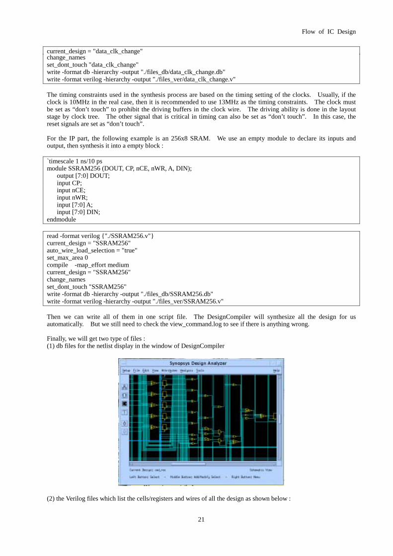
current_design = "data_clk_change" change_names set_dont_touch "data_clk_change" write -format db -hierarchy -output "./files_db/data_clk_change.db" write -format verilog -hierarchy -output "./files_ver/data_clk_change.v" The timing constraints used in the synthesis process are based on the timing setting of the clocks. Usually, if the clock is 10MHz in the real case, then it is recommended to use 13MHz as the timing constraints. The clock must be set as “don’t touch” to prohibit the driving buffers in the clock wire. The driving ability is done in the layout stage by clock tree. The other signal that is critical in timing can also be set as “don’t touch”. In this case, the reset signals are set as “don’t touch”. For the IP part, the following example is an 256x8 SRAM. We use an empty module to declare its inputs and output, then synthesis it into a empty block : `timescale 1 ns/10 ps module SSRAM256 (DOUT, CP, nCE, nWR, A, DIN); output [7:0] DOUT; input CP; input nCE; input nWR; input [7:0] A; input [7:0] DIN; endmodule read -format verilog {"./SSRAM256.v"} current_design = "SSRAM256" auto_wire_load_selection = "true" set_max_area 0 compile -map_effort medium current_design = "SSRAM256" change_names set_dont_touch "SSRAM256" write -format db -hierarchy -output "./files_db/SSRAM256.db" write -format verilog -hierarchy -output "./files_ver/SSRAM256.v" Then we can write all of them in one script file. The DesignCompiler will synthesize all the design for us automatically. But we still need to check the view_command.log to see if there is anything wrong. Finally, we will get two type of files : (1) db files for the netlist display in the window of DesignCompiler
(2) the Verilog files which list the cells/registers and wires of all the design as shown below :

Flow of IC Design
22
module clockgen ( CLOCK , IOCLOCK , XRESETA , XTAL1I , SEL6T , XIDLE , EAI , XPOR , OSCEN , ENCLK , RESETI , IOCLOCK_2_1 ); output CLOCK ; output IOCLOCK ; input XRESETA ; input XTAL1I ; input SEL6T ; input XIDLE ; input EAI ; input XPOR ; input OSCEN ; output ENCLK ; input RESETI ; input IOCLOCK_2_1 ; TFCN1 Q_CLK2_reg (.CDN(XRESETA), .CP(VALID_CLK), .Q(Q_CLK2), .QN(AVANT_UNCONNECTED_1)); TFCN1 OSCCT0_reg (.CDN(n1328), .CP(CTCLK), .Q(AVANT_UNCONNECTED_0), .QN(n1316)); IND2D1 U569 (.A1(OSCEN), .B1(XRESETCT), .ZN(n1327)); IND2D1 U573 (.A1(IOCLOCK_2_1), .B1(XIDLE), .ZN(CLOCK)); AOI22D0 U578 (.A1(Q_CLK2), .A2(n1325), .B1(VALID_CLK), .B2(n1326), .ZN(n1329)); DFCN1 OSCCT8_reg (.CDN(n1328), .CP(n1306), .D(n1317), .Q(AVANT_UNCONNECTED_16), .QN(n1317)); DFCN1 OSCCT15_reg (.CDN(n1328), .CP(n1307), .D(n1314), .Q(AVANT_UNCONNECTED_15), . QN(n1314)); DFCN1 OSCCT6_reg (.CDN(n1328), .CP(n1308), .D(n1319), .Q(AVANT_UNCONNECTED_14), .QN(n1319)); DFCN1 OSCCT2_reg (.CDN(n1328), .CP(n1309), .D(n1320), .Q(AVANT_UNCONNECTED_13), .QN(n1320)); DFCN1 OSCCT11_reg (.CDN(n1328), .CP(n1310), .D(n1315), .Q(AVANT_UNCONNECTED_12), .QN(n1315)); DFCN1 OSCCT4_reg (.CDN(n1328), .CP(n1311), .D(n1313), .Q(AVANT_UNCONNECTED_11), .QN(n1313)); DFCN1 OSCCT13_reg (.CDN(n1328), .CP(n1312), .D(n1318), .Q(AVANT_UNCONNECTED_10), .QN(n1318)); DFCN1 OSCCT5_reg (.CDN(n1328), .CP(n1313), .D(n1308), .Q(AVANT_UNCONNECTED_9), .QN(n1308)); DFCN1 OSCCT12_reg (.CDN(n1328), .CP(n1315), .D(n1312), .Q(AVANT_UNCONNECTED_8), .QN(n1312)); DFCN1 OSCCT1_reg (.CDN(n1328), .CP(n1316), .D(n1309), .Q(AVANT_UNCONNECTED_7), .QN(n1309)); DFCN1 OSCCT9_reg (.CDN(n1328), .CP(n1317), .D(n1321), .Q(AVANT_UNCONNECTED_6), .QN(n1321)); DFCN1 OSCCT14_reg (.CDN(n1328), .CP(n1318), .D(n1307), .Q(AVANT_UNCONNECTED_5), .QN(n1307)); DFCN1 OSCCT7_reg (.CDN(n1328), .CP(n1319), .D(n1306), .Q(AVANT_UNCONNECTED_4), .QN(n1306)); DFCN1 OSCCT3_reg (.CDN(n1328), .CP(n1320), .D(n1311), .Q(AVANT_UNCONNECTED_3), .QN(n1311)); DFCN1 OSCCT10_reg (.CDN(n1328), .CP(n1321), .D(n1310), .Q(AVANT_UNCONNECTED_2), .QN(n1310)); INV0 U576 (.I(XTAL1I), .ZN(n1324)); INV0 U579 (.I(n1325), .ZN(n1326)); BUF1 U571 (.I(n1329), .Z(IOCLOCK)); AN2D2 U572 (.A1(OSCEN), .A2(XRESETCT), .Z(n1328)); ND2D0 U575 (.A1(SEL6T), .A2(EAI), .ZN(n1325)); NR2D0 U574 (.A1(ENCLK), .A2(n1324), .ZN(CTCLK)); NR2D0 U577 (.A1(n1324), .A2(n1322), .ZN(VALID_CLK)); DFCSN1 OSCCT16_reg (.CDN(n1327), .CP(n1314), .D(n1322), .Q(ENCLK), .QN(n1322), .SDN(XRESETCT)); INR2D1 U570 (.A1(XPOR), .B1(RESETI), .ZN(XRESETCT)); endmodule Some modules are derived from Synopsys design-ware. The functions such as addition, multiplication, increment, etc., will be synthesized with the design-ware. There are two synthesis style : bottom-up and top-down. If we synthesize the entire design from the lowest modules, set “don’t touch” on them, then synthesize the higher modules. It is called the bottom-up style. An obvious advantage of this style is that the netlist is in hierarchical, easy to be read. The other one is that we can synthesize some modules of the entire design only without re-synthesizing them all. If we synthesize the entire design from the top module, it is called top-down style. The advantage is that the connection circuits between modules will be optimized.

Flow of IC Design
23
The following example is a 4-bit counter with initial value. The code is (all the comments are canceled for space saving) module counter_4b (xhwrst, sysclk, ini_value, counter_out); input xhwrst, sysclk; input [3:0] ini_value; output [3:0] counter_out; reg [3:0] counter_out; always @ (negedge xhwrst or posedge sysclk ) begin if ( !xhwrst ) begin
counter_out <= ini_value; end
else begin counter_out <= counter_out + 1;
end end endmodule The script files is read -format verilog {"./counter_4b.v"} current_design = "counter_4b" auto_wire_load_selection = "true" set_fix_multiple_port_nets -all -buffer_constants create_clock -name "sysclk" -period 60 -waveform { "0" "30" } { "sysclk" } set_dont_touch_network find( clock, "sysclk") set_dont_touch_network find( port, "xhwrst") set_clock_skew -uncertainty 0.5 -ideal sysclk set_output_delay 5 -max -clock sysclk all_outputs() set_output_delay 1 -min -clock sysclk all_outputs() set_max_area 0 compile -map_effort medium current_design = "counter_4b" change_names set_dont_touch "counter_4b" write -format db -hierarchy -output "./counter_4b.db" write -format verilog -hierarchy -output "./files_ver/counter_4b.v" The synthesized netlist are given below module counter_4b ( xhwrst, sysclk, ini_value_3, ini_value_2, ini_value_1, ini_value_0, counter_out_3, counter_out_2, counter_out_1, counter_out_0 ); input xhwrst, sysclk, ini_value_3, ini_value_2, ini_value_1, ini_value_0;
: a module Top-down synthesis Bottom-up synthesis

Flow of IC Design
24
output counter_out_3, counter_out_2, counter_out_1, counter_out_0; wire n96, n97, n98, n99, n100, n101, n102, n103, n104, n105, n106, n107, n108, n109, n110, n111, n112, n113, n114, n115, n116, n117, n118, n119, net5, n120, n121, n122; INV0 U21 ( .I(ini_value_3), .ZN(n108) ); INV0 U22 ( .I(ini_value_2), .ZN(n109) ); INV0 U23 ( .I(ini_value_1), .ZN(n110) ); INV0 U24 ( .I(ini_value_0), .ZN(n111) ); XNR2D1 U25 ( .A1(n106), .A2(net5), .ZN(n120) ); NR2D0 U26 ( .A1(n107), .A2(n97), .ZN(n106) ); ND2D0 U27 ( .A1(counter_out_1), .A2(counter_out_0), .ZN(n107) ); INV1 U28 ( .I(n98), .ZN(n119) ); INV1 U29 ( .I(n99), .ZN(n118) ); INV1 U30 ( .I(n100), .ZN(n117) ); INV1 U31 ( .I(n101), .ZN(n116) ); INV1 U32 ( .I(n102), .ZN(n115) ); INV1 U33 ( .I(n103), .ZN(n114) ); INV1 U34 ( .I(n104), .ZN(n113) ); INV1 U35 ( .I(n105), .ZN(n112) ); NR2D1H U36 ( .A1(xhwrst), .A2(n108), .ZN(n105) ); NR2D1H U37 ( .A1(ini_value_3), .A2(xhwrst), .ZN(n104) ); NR2D1H U38 ( .A1(xhwrst), .A2(n109), .ZN(n103) ); NR2D1H U39 ( .A1(ini_value_2), .A2(xhwrst), .ZN(n102) ); NR2D1H U40 ( .A1(xhwrst), .A2(n110), .ZN(n101) ); NR2D1H U41 ( .A1(ini_value_1), .A2(xhwrst), .ZN(n100) ); NR2D1H U42 ( .A1(xhwrst), .A2(n111), .ZN(n99) ); NR2D1H U43 ( .A1(ini_value_0), .A2(xhwrst), .ZN(n98) ); XOR2D1 U44 ( .A1(n107), .A2(n97), .Z(n121) ); XOR2D1 U45 ( .A1(counter_out_0), .A2(counter_out_1), .Z(n122) ); DFCSN1 counter_out_reg_3 ( .D(n120), .CP(sysclk), .SDN(n112), .CDN(n113), .Q(counter_out_3), .QN(net5) ); DFCSN1 counter_out_reg_2 ( .D(n121), .CP(sysclk), .SDN(n114), .CDN(n115), .Q(counter_out_2), .QN(n97) ); DFCSN1 counter_out_reg_1 ( .D(n122), .CP(sysclk), .SDN(n116), .CDN(n117), .Q(counter_out_1) ); DFCSN1 counter_out_reg_0 ( .D(n96), .CP(sysclk), .SDN(n118), .CDN(n119), .Q(counter_out_0), .QN(n96) ); endmodule

Flow of IC Design
25
12. Pre-sim SDF Generation Now we will do simulation again. This time, the target of the simulation is not the HDL source code, but the netlist in Verilog. The netlist is the list showing all the cells and registers in this design, and the wires which connect them. Functionally, it should work the same as the source code does. But in this stage, the timing issue is added. So it is not the behavioral simulation that simulates the functions only. It is closer to the performance of the real chip. Now the timing is added to the cells and registers only. The timing is provided by the cell library where each cell has its own timing in one condition. The timing for the wire can not be estimated because there is the information of connection only, no information about the wire length and width. Because this simulation is done before the chip layout, it is call pre-layout simulation, or just pre-sim. The file containing the timing information of all the cells is called the standard delay file (SDF). SDF is easy to be derived from the netlist by using Synopsys DesignCompiler. Just setting the simulation condition such as best-case (0oC) commercial or worst-case (125oC) commercial, etc., and using the Synopsys command “write_sdf”, the SDF can be derived quickly. The following paragraph is an example which shows part of the SDF : ) (CELL (CELLTYPE "DFCN1") (INSTANCE sd_card_top_ins/data_clk_change_ins/buf14_reg_7) (DELAY (ABSOLUTE (IOPATH (posedge CP) Q (0.856:0.856:0.856) (0.886:0.886:0.886)) (IOPATH (posedge CP) QN (0.990:0.990:0.990) (0.957:0.957:0.957)) (IOPATH (negedge CDN) QN (51.970:51.970:51.970) ()) ) ) (TIMINGCHECK (WIDTH (posedge CP) (0.586:0.586:0.586)) (WIDTH (negedge CP) (0.670:0.670:0.670)) (SETUP (posedge D) (posedge CP) (0.529:0.541:0.541)) (SETUP (negedge D) (posedge CP) (0.514:0.542:0.542)) (HOLD (posedge D) (posedge CP) (-0.001:0.000:0.000)) (HOLD (negedge D) (posedge CP) (-0.005:-0.007:-0.007)) (RECOVERY (posedge CDN) (posedge CP) (0.000:0.000:0.000)) (HOLD (posedge CDN) (posedge CP) (31.626:31.626:31.626)) (WIDTH (posedge CDN) (0.000:0.000:0.000)) (WIDTH (negedge CDN) (0.846:0.846:0.846)) ) By checking the SDF, we find that the delay for the “don’t touch” paths, basically clocks and resets, are extremely high. The reason is that the number of fanouts of these paths is very large, one path can not drive so many fanouts. In the real chip, these paths are replaced by trees. In the netlist before layout, there is no information about tree. Therefore, we can insert a empty tree in the netlist as below : Because tree_a is empty, there is no timing information for clk_a. When we do the simulation, tree_a is change to the HDL code clk <= clk_pre_a. So that, clk_a will drive all the fanouts with infinite driving ability. With the netlist, SDF, the original test bench plus the IP simulation models, the pre-sim can be run in the same way as the RTL-sim does.
clk_a clk_pre_a clk_a tree_a

Flow of IC Design
26
13. Pre-Simulation The simulation tools used here are the same as those in the RTL simulation, both Cadence Verilof-XL and ModelSim can do this job. Even though the test bench is the same in both RTL-sim and pre-sim, we need to add one line in the test bench : $sdf_annotate("/yyy/xxx.sdf",top_tb_ins); where yyy is the directoty, xxx is the SDF name and top_tb_ins is the instance name of the top test bench. With this, the simulation tool will read the SDF and add the timing to the waveform. This process is called annotation. It is very obvious that the waveform is different from that of RTL-sim. The timing delay is obviously appearing. An example of the waveform from the pre-sim is shown below :
If the results is not as expected, then we know the function is correct, but the timing can not be met. This always happens in the cases that the clock speed is very high, or the asynchronous design is used. The best way to solve these problems is to re-design the source code. If the clock speed is two high and there is a path that goes through too many gates, we can divide the function into several paths. Usually, if the FPGA verification is passed, the problem of high speed clock will not exist because FPGA is slower than the cells provided by the foundries, especially we have adopted 0.35um – 0.18um technology in the recent years. As for the asynchronous design, it is hard to be controlled, no matter the cell is fast or slow. Ex : The half-cycle pulse for the SRAM write enable Min. (best) case Typical case Max. (Worst) case We may also find that there is the new message happening called timing violation. This message indicates the instability of signal latch. Their major phenomena are the setup time, hold time and reset/set pulse width.
data data data

Flow of IC Design
27
Set-up time violation hold time violation width violation for reset The timing of these parameters depends on the cell library. The message also indicates when the violation happens. We can use the violation information to locate the timing problem in the design. The following paragraph is an example for the timing violation : "/diska1/user/ba017/KIT/tcb773s/verilog/tcb773s.v", 2738: Timing violation in tb_top.all_top_ins.sd_card_top_ins.FlashCtrl_8B_ins.DlyRB1_reg $hold( posedge CP:247058188, negedge D &&& CP_check:247058197, 0.13 : 13 ); Not all of the violation must be modified. If one violation will not influence the function, then this one can be ignored. Ex : data latch clock latch counter 1 0 1 0 1 data gen. clock data to be latched Timing violation : data latched here is unstable but it will not be used.
data data

Flow of IC Design
28
14. Layout Guide Writing With careful check of the pre-sim results, the netlist is ready for layout. Usually, the IC designers will not do this step by themselves. The layout job is done by the layout engineers. The following items are the information we need to tell the layout people : 1. The pin assignment and location around the chip 2. The special requirement for the pads.
Ex : If this chip will be mounted on board by the chip on board (COB) style, then the pad can not be too small for wire bonding.
3. The trees of the” don’t touch” nets. 4. The modules that are needed to be placed together.
Ex : The IP of USB PHY must be placed close to its I/O pins and the USB serial interface engine (SIE). 5. The layer of mental and poly (Ex : 1P3M :one layer of ploy, 3 layer of metal. If 2P, our example is for the
projects with flash memory) 6. Some other information
Ex : The electro-static discharge (ESD) protection circuits on the 4 corners Ex : The width of scribe lines Ex : Adding the seal ring for protection
Layout Pin Assignment
1 Ptest select 0 I 23 Phostclk I 44 Pp2 0 B 66 Pxfce 1 O2 Ptest select 1 I 24 VSSI 45 Pp2 1 B 67 VSSO 3 Ptest select 2 I 25 VSSI 46 Pp2 2 B 68 VSSO 4 Ptest select 3 I 26 Pdat0 bus B 47 Pp2 3 B 69 Pf data 0 B5 Pevent occur B 27 Pdat1 bus B 48 Pp2 4 B 70 Pf data 1 B6 Pp0 0 B 28 VDDO 49 Pp2 5 B 71 Pf data 2 B7 Pp0 1 B 29 VDDO 50 Pp2 6 B 72 Pf data 3 B8 Pp0 2 B 30 VDDA 51 Pp2 7 B 73 VDDO 9 Pp0 3 B 31 Res in I 52 Pprosc thru I 74 VDDO
10 Pp0 4 B 32 VSSA 53 Pxfce 2 O 75 Pf data 4 B11 Pp0 5 B 33 VSSO 54 Pxfce 3 O 76 Pf data 5 B12 Pp0 6 B 34 VSSO 55 Pxfce 4 O 77 Pf data 6 B13 Pp0 7 B 35 Pxhwrst I 56 Pxfce 5 O 78 Pf data 7 B14 Pp1 0 B 36 VDDI 57 Pxfce 6 O 79 VSSI 15 Pp1 1 B 37 VDDI 58 Pp3 0 B 80 VSSI 16 Pp1 2 B 38 Pfrxb I 59 Pp3 1 B 81 Pdat2 bus B17 Pp1 3 B 39 Pxfre O 60 Pp3 2 B 82 Pdat3 bus B18 Pp1 4 B 40 Pxfce 0 O 61 Pp3 3 B 83 VDDI 19 Pp1 5 B 41 Pfcle O 62 Pp3 4 B 84 VDDI 20 Pp1 6 B 42 Pfale O 63 Pp3 5 B 85 Pcmd bus B21 Pp1 7 B 43 Pxfwe O 64 Pp3 6 B 22 Pxfce 7 O 65 Pp3 7 B

Flow of IC Design
29
Clock Tree
IP used :
4 SSRAM512 (512x8), 1 SSRAM272 (272x8), 1 SSRAM128 (128x8), 1 porcell3, 1 PROSC2, 1
ROM12K, 1 LVRAM256.
Netlist for layout : diska1/USER/ba057/sd_card_3/netlist/all_top.v
sd_card_top_ins
sd_sysclk
Fanout=1690
U1565(INV0)
ZN
xhwrst
Fanout=2456
U1550(INV0)
ZN
hostclk
Fanout=787
register_ins
xswrst
Fanout=608
Q xswrst_reg(DFSN3)
all_top/U1565/ZN :
BUF3(1) -> BUF5(5) -> BUF5(85)
all_top/U1550/ZN :
BUF3(1) -> BUF5(7) -> BUF5(125)
all_top/U1347/ZN :
BUF3(1) -> BUF3(5) -> BUF5(40)
all_top/sd_card_top_ins/register_ins
/xswrst_reg/Q :
BUF3(1) -> BUF3(7) -> BUF3(61)
C
U1374(INR2D0)
srtst_clk
Fanout=6
U1317(ND2D0)
ZN all_top/U1317/ZN :
BUF3(1)
1
22 23 43
44
65 66 85

Flow of IC Design
30
15. Chip Layout Most of our designs are layout by auto placement and routing (APR). In a simple way, APR can be explained as : 1. choosing a suitable size for the entire chip. (There are two ways that the chip size is determined : pad limited or
core limited. If the chip size is determined by the gate count plus the IPs, then the chip is core limited. If there are too many I/O pins that the pads around the chip defines the chip size, then it is pad limited. For pad limited cases, the core part may be very loose, more function can be added so the chip area will not be wasted)
2. putting the pads in the correct place by hands 3. putting the IPs in the suitable place by hand. (Those IPs in the netlist are empty. They are inserted in the
layout stage) 4. place the VCC(VDD) and GND(VSS) paths. 5. creating clock and reset trees, and placing all the cells and registers in the netlist (our digital design part) to the
empty place by EDA tools. (Our APR tool is Avant! Apollo)

Flow of IC Design
31
16. 17. SPF and SDF generation After the chip layout, a new netlist will be generated according to the real wires in the chip. The most obvious difference between this netlist and the pre-sim netlist is the clock and reset trees are placed in this netlist. Tree before layout Tree after layout Since the netlist is changed, we need to do the simulation again. It is called the post-layout simulation, or post-sim, that will be discussed in the next step. This time, not only the cell/register delay will be taken, but also the wire delay is calculated for the more accurate simulation. The wire delay is estimated from the length, width and via between metal layers, etc., of a wire. All of these will be shown quantitatively as its resistance and capacitance. So the layout engineers will extract the parasitic capacitance and resistance from the layout with certain EDA tools. The tools we used is StarRC of Avant!. The file containing these information is called the standard parasitic file (SPF). The following paragraph is an example for SPF. *|NET sd_card_top_ins/register_ins/clear_reg_1 1.13e-01PF *|I (F43719 sd_card_top_ins/register_ins/clear_reg_reg_1 Q O 0 2376.85 2190.85) *|I (F39982 sd_card_top_ins/register_ins/U16613 B2 I 1.221e-14 2458.1 1845.05) *|I (F31375 sd_card_top_ins/register_ins/U16987 A1 I 8e-15 2193.1 2311.25) Cg65611 F43719 0 4.94324e-14 Cg65612 F39982 0 3.69553e-14 Cg65613 F31375 0 2.68559e-14 R64125 F43719 F39982 73.736 R64126 F43719 F31375 59.1218 R64127 F39982 F31375 1296.45 *|NET sd_card_top_ins/data_clk_change_ins/n4541 8.00e-03PF *|I (F27235 sd_card_top_ins/data_clk_change_ins/U2667 Z O 0 2566.85 2742.9) *|I (F28670 sd_card_top_ins/data_clk_change_ins/buf14_reg_0 D I 6.55e-15 2566.85 2780.25) Cg65614 F27235 0 5.19058e-15 Cg65615 F28670 0 2.80581e-15 R64128 F27235 F28670 11.3165 *|NET sd_card_top_ins/data_clk_change_ins/n4496 6.93e-03PF *|I (F27055 sd_card_top_ins/data_clk_change_ins/U2622 Z O 0 2566.85 2754.1) *|I (F28445 sd_card_top_ins/data_clk_change_ins/buf07_reg_5 D I 6.55e-15 2556.85 2781.65) Cg65616 F27055 0 4.33082e-15 Cg65617 F28445 0 2.59936e-15 R64129 F27055 F28445 10.4807 From SPF, we can generate the SDF similar to the SDF of pre-sim but with accurate timing for each wire. The generation procedures are : 1. The EDA tool is Avant! PrimeTime (PT). 2. Write a script file to read the parasitic RC parameters from SPF and annotate them to the SDF. An example of
the script file is as follows (assume the name for the design is our_design) (this example is for the best case)
set search_path "/diska1/user/ba017/KIT/tcb773s/synopsys" set link_path {* /diska1/user/ba017/KIT/tcb773s/synopsys/tcb773sbc.db} read_verilog {../../verilog-out/our_desin.v} current_design our_design read_parasitics {../../star_rc/dspf/our_design.spf}

Flow of IC Design
32
report_annotated_parasitics -check > annotate.report write_sdf {../sdf/our_design_bc_pt.sdf} exit We can use “ pt_shell –f ” to run this script
3. Log the process in a file and check them to see if there is anything unreasonable. The usual errors and warnings are Error : unconnected nets from the design ware Ex : Error: Cannot find net 'uctop/Iperipheral/net2265' in design 'ba057' (DES-002) Error: Cannot find net 'uctop/Iperipheral/net2291' in design 'ba057' (DES-002) Error: Cannot find net 'uctop/Icpu8052/Idata_path/net1894' in design 'ba057' (DES-002) Warning : unconnected hierarchy pin Ex :
Warning: Unconnected hierarchy pin 'sd_card_top_ins/status_ins/status_reg_0' is missing in the RC annotation for net 'sd_card_top_ins/status_ins/status_reg_0'. (PARA-007) Warning: Unconnected hierarchy pin 'sd_card_top_ins/status_ins/status_reg_1' is missing in the RC annotation for net 'sd_card_top_ins/status_ins/status_reg_1'. (PARA-007) Warning: Unconnected hierarchy pin 'sd_card_top_ins/status_ins/status_reg_2' is missing in the RC annotation for net 'sd_card_top_ins/status_ins/status_reg_2'. (PARA-007) Warning : nets connected to VDD Ex : Warning: Failed to compute C-effective for the timing arc (tcb773swc/INV0) uctop/Idatabus_mux/U328/I-->ZN (falling negative-unate) because the library data indicates a non-positive drive resistance. [r/f inp_slew = 0/0, out_cap = 0.014488 (lib units)] (RC-004)
Warning: Failed to compute C-effective for the timing arc (tcb773swc/INV0) uctop/Idatabus_mux/U192/I-->ZN (falling negative-unate) because the library data indicates a non-positive drive resistance. [r/f inp_slew = 0/0, out_cap = 0.0155054 (lib units)] (RC-004) The number of not-annotated nets
Pin type Total RC pi RC network Not Annotated internal net driver 23754 0 22984 770design input port 52 0 52 0
23806 0 23036 770 If everything is reasonable, then this SDF can be used for post-sim.

Flow of IC Design
33
18. Post-simulation In most of the cases, the post-sim results are very close to the pre-sim results, especially when we follow the rule of synchronous design. If there is some problem happening in this step, it may be a headache because we may go back to modify our source code and re-do all the flow again! The procedures of running post-sim are exactly the same as running pre-sim. The post-sim SDF is declared in the test bench, and the timing will be annotated when the simulation is started. Usually we like to check the clock skew at first. An example of the waveform of the clock skew is shown below, where the clock skew is 0.05 ns :
The timing violation may also happen in post-sim stage. Also, if one violation will not influence the function, then this one can be ignored.

Flow of IC Design
34
19. LVS Check LVS stands for layout versus schematics. The APR-style layout is to route all the nets that connect the ports of the cells, registers and macros in the entire netlist. The layout tool does not care what cells they are. So the tool will only check if the wire connection is correct or not. As for the cells, they are just like black boxes. Therefore, after the post-sim, we need to create a file that contains all the information about the chip. The layout engineers can compare this file with their layout results. The file we will prepare is the LVS file. The EDA tool for the comparison is the Cadence Dracula. Ex : The contents of the LVS file are not only the nets, but also all the cells in HSPICE models (xxx.spi). So this file can be compared with the results extracted from the chip layout, which is also in the HSPICE format. The following paragraphs are examples of part of the spi file : An AND gate .SUBCKT AN2D2 Z A1 A2 M1 U2_U7_DRAIN A2 VSS VSS NL L=.35U W=2.10U M2 U2_OUT A1 U2_U7_DRAIN VSS NL L=.35U W=1.84U M3 U2_OUT A1 VDD VDD PL L=.35U W=3.00U M4 U2_OUT A2 VDD VDD PL L=.35U W=3.00U M5 Z U2_OUT VSS VSS NL L=.35U W=3.00U M6 Z U2_OUT VDD VDD PL L=.35U W=6.00U M7 Z U2_OUT VSS VSS NL L=.35U W=3.00U M8 Z U2_OUT VDD VDD PL L=.35U W=6.00U .ENDS AN2D2 A flip-flop .SUBCKT DFCSN2 Q QN CDN CP D SDN M1 U9_S INCP O2 VDD PL L=.35U W=1.40U M2 U9_S INCPB O2 VSS NL L=.35U W=1.10U M3 U7_S INCPB MFB VDD PL L=.35U W=1.40U M4 U7_S INCP MFB VSS NL L=.35U W=1.10U M5 INDB INCP U7_S VDD PL L=.35U W=2.80U M6 INDB INCPB U7_S VSS NL L=.35U W=1.80U M7 IND INCPB U9_S VDD PL L=.35U W=2.60U M8 IND INCP U9_S VSS NL L=.35U W=1.80U M9 QN O2 VSS VSS NL L=.35U W=3.00U M10 QN O2 VDD VDD PL L=.35U W=5.70U M11 INCPB CP VSS VSS NL L=.35U W=1.90U M12 INCPB CP VDD VDD PL L=.35U W=4.30U M13 INCP INCPB VSS VSS NL L=.35U W=1.90U M14 INCP INCPB VDD VDD PL L=.35U W=4.30U M15 INDB D VSS VSS NL L=.35U W=1.00U M16 INDB D VDD VDD PL L=.35U W=2.50U M17 QN O2 VSS VSS NL L=.35U W=3.00U M18 QN O2 VDD VDD PL L=.35U W=5.70U M19 Q O1 VSS VSS NL L=.35U W=3.00U M20 Q O1 VDD VDD PL L=.35U W=5.70U M21 Q O1 VSS VSS NL L=.35U W=3.00U M22 Q O1 VDD VDD PL L=.35U W=5.70U M23 U14_U7_DRAIN CDN VSS VSS NL L=.35U W=1.80U M24 MFB IND U14_U7_DRAIN VSS NL L=.35U W=1.80U M25 MFB IND VDD VDD PL L=.35U W=2.25U M26 MFB CDN VDD VDD PL L=.35U W=2.25U
Cell1 Cell3
Cell2
Net123
Net124 Net127
Net125 Net126

Flow of IC Design
35
M27 U13_U7_DRAIN SDN VSS VSS NL L=.35U W=3.00U M28 IND U7_S U13_U7_DRAIN VSS NL L=.35U W=3.00U M29 IND U7_S VDD VDD PL L=.35U W=3.75U M30 IND SDN VDD VDD PL L=.35U W=3.75U M31 U12_U7_DRAIN CDN VSS VSS NL L=.35U W=3.00U M32 O1 U9_S U12_U7_DRAIN VSS NL L=.35U W=3.00U M33 O1 U9_S VDD VDD PL L=.35U W=3.75U M34 O1 CDN VDD VDD PL L=.35U W=3.75U M35 U15_U7_DRAIN SDN VSS VSS NL L=.35U W=3.00U M36 O2 O1 U15_U7_DRAIN VSS NL L=.35U W=3.00U M37 O2 O1 VDD VDD PL L=.35U W=3.75U M38 O2 SDN VDD VDD PL L=.35U W=3.75U .ENDS DFCSN2 A module in the design .SUBCKT spi_mode_DW01_cmp2_8_5 A_7 A_6 A_5 A_4 A_3 A_2 A_1 A_0 + B_7 B_6 B_5 B_4 B_3 B_2 B_1 B_0 LEQ TC LT_LE GE_GT XU11 n58 A_7 INV0 XU12 n57 A_4 INV0 XU8 n53 n56 n57 ND2D0 XU7 n55 A_3 A_2 NR2D0 XU9 n56 A_6 A_5 NR2D0 XU10 LT_LE n53 n54 NR2D0 XU6 n54 n55 B_4 n58 OAI21D0 .ENDS Actually, Dracula can not compare the spi file with layout results directly. We need to use one utility in Dracula called LOGLVS to convert the spi file into an unreadable binary file. Then is file is sent to layout engineers for the comparison.

Flow of IC Design
36
20. 21. Tape-out for Mask Tooling and Fabrication After all the jobs done, our design is ready for the chip fabrication. The duties of design engineers are close to the end. Before, all the information for the foundries is recorded in the tape and sent out. So here came the terminology “tape-out”. We give a very simple description about the mask/ fabrication processes based on one example. There are 13 layers of masks in this example. The procedures are : 1. The mask is made according to the layout. Each layer has its own mask made from a chromium-plated glass. 2. In this example, the wafer is the p-substrate. For 8-inch wafer, the thickness is about 35mil (1 mil = 25.4υm)
cut from ingot. 3. In the beginning, the wafer is coated with a layer of positive photo resistor. 4. The wafer is put under the light through one mask. The region that is exposed will be stripped or dipped 5. The dipped region is stuffed with certain materials, then covered by the insulator. 6. These procedures are repeated until all layers are done. The process from tape-out to chip ready is called non-recursive engineering (NRE). It takes about 1.5 – 2.5 months now. The NRE charge is very high, about USD50K – 70K for 0.35um, USD200K – 300K for 0.18um. If there is any problem found after the chip is done, and this problem is caused by the error from the designers, the designers must take the full responsibility for the loss of money and time. So the pressure for the designer is very heavy. No matter how detailed we verified in the simulation or FPGA stage, no one can guarantee a chip of 100% well. Because of the high cost for NRE, many foundries provide the multi-chip service, or it is called shuttle. The NRE is not for our design only. It gathers many design from the different companies, then make them into one wafer together. After the fabrication, each company can get its own chips back. The cost is much lower than the formal NRE. Taking shuttle in the first tape-out is a good choice to reduce the risk of the later formal tape-out. Even though the shuttle costs much less than the NRE does, most of the schools can not afford that, either. In Taiwan, an organization called National Science Committee (NSC) will negotiate with the big foundries such as TSMC and UMC about the shuttle for school only. It is totally free charge, just for the purpose of education.
p-substrate
P- N-
N+ N+ P+ P+
Field Oxide
Low Temperature Oxide
NMOS PMOS
P Well N WellThin Oxide
N Implant P Implant
Poly
Poly Poly
Contact
Metal 1
Metal 3
Metal 2
Via 1
Via 2
passivation
mask
lens
wafer
pad

Flow of IC Design
37
22. Test Pattern Generation The only way to know if the chip is OK or not is that the chip is tested before it is packaged and mounted in the PC board. The machine used to test the chip is called tester. The principle of tester is very simple : 1. send the power to the chip, 2. after reset, give the prepared input, 3. observe the output and compare them with the expected value (High or Low). 4. if the comparison for any single output is not matched, then this chip may contain some false functions. Those prepared inputs patterns (0 or 1) and the expected output patterns (H or L) together are called the test patterns. An example of the test pattern is shown below : (an IC with 67 pins except for the VDD and GND) 39893 10100111111111111111011111110000111111H110111LHHHHHHHLLLH1011100110 39894 10100101111111111111011111110000010111H111110LHHHHHHHLLLH1011100110 39895 10100111111111111111011111110000010111H110111LHHHHHHHLLHH1111111110 39896 10100101111111111111011111110000010111H111110LHHHHHHHLLHH1111111110 39897 10100111111111111111011111110000010111H110111LHHHHHHHLLLH1011011000 39898 10100101111111111111011111110000010111H111110LHHHHHHHLLLH1011011000 39899 10100111111111111111011111110000010111H110111LHHHHHHHLLHH1111111110 39900 10100101111101011001011111110000111111H111110LHHHHHHHLLHH1111111110 39901 10100111111101011001011111110000111111H110111LHHHHHHHLLLH1000101010 39902 10100101111111111111011111110000111111H110110LHHHHHHHLLLH1000101010 39903 10100111111111111111011111110000111111H110111LHHHHHHHLLHH1111111110 39904 101001011111LLLLLLLL011111110000111111H110100LHHHHHHHLLHH1111111110 39905 101001111111LLLLLLLL011111110000111111H110101LHHHHHHHLLLH1001100100 39906 101001011111LLLLLLLL011111110000111111H110100LHHHHHHHLLLH1001100100 39907 101001111111LLLLLLLL011111110000111111H110101LHHHHHHHLLHH1111111110 39908 101001011111LLLLLLLL011111110000111111H110100LHHHHHHHLLHH1111111110 39909 101001111111LLLLLLLL011111110000111111H110101LHHHHHHHLLLH1001100010 39910 10100101111111111111011111110000111111H110110LHHHHHHHLLLH1001100010 39911 10100111111111111111011111110000111111H110111LHHHHHHHLLHH1111111110 39912 10100101111111111111011111110000010111H111110LHHHHHHHLLHH1111111110 39913 10100111111111111111011111110000010111H110111LHHHHHHHLLLH1011000100 The sequence and the ways of generating the inputs are giving in the following guide : Signal name Type Grouppxhwrst I 1ptest select 0 I 2ptest select 1 I 2ptest select 2 I 2ptest select 3 I 2pprosc thru I 2phostclk I 3pcmd bus B 4pdat0 bus B 4pdat1 bus B 4pdat2 bus B 4pdat3 bus B 4pp0 0 B 2pp0 1 B 2pp0 2 B 2 …………… … …pf data 7 B 6pevent occur B 6

Flow of IC Design
38
One cycle should be longer than 200 ns (Tester frequency > 5MHz) D1 : 5 ns D2 : 0 ns D3 : 50 ns D4 : 55 ns D5 : 20 ns D6 : 25 ns Since the test pattern is used to test the cells and nets, an important issue about the test pattern is the function coverage. The higher the coverage is, the better yield we can provide to the customers. For the large chip, the 100% coverage is almost impossible in a short pattern. Instead, we ask for certain degree of toggle rate. We make every net toggled ( goes from 0 to 1, or vice versa), observe the output to see if there is any fault such as stuck-at-zero, stuck-at-one, etc. The high toggle rate is easier to be reached. Usually, 70 – 90% is not difficult. In the recent years, it is recommended that the test pattern should not be the same as the simulation pattern. We need to prepare a different set of pattern, with the help of some extra circuits inside the chip, for a better coverage and shorter time. The pattern will not be generated by us, it is generate by the EDA tools, so the process is call auto test pattern generation (ATPG). The extra circuits, e.g. some scan chains and scan flip-flops, will increase the die size of the chip (it may be 20% larger). So we need to be aware of this point. We can do this with Synopsys TestCompiler. The knowledge about this field is called design for testability (DFT). It will be discussed in the later course.
Basic Cycle
Group 1
Group 2
Group 3
Group 4
Group 5
Group 6
Strobe region : 75% of a cycle
D1
D3
D4
D5
D6

Flow of IC Design
39
23. 24. Chip Probe and Final Test The tester is a machine composed of several insertion cards. There are several channels in each card. Every channel can be one input signal to one input port of the chip with input test patterns. Or the channel can be configured as one output signal connected to one output port of the chip, compares the received data with the expected output patterns. Those input/output test patterns are stored in the memory of the cards. Take the tester we are using now as the example, the total channel number is 256, the memory depth of each channel is 1M cycles. HP and Teradyn are the famous tester manufacturers. The connector that connects the channels to one chip of the wafer is called the probe card. The probe card will move vertically and horizontally around the wafer. Every time it moves to one chip, the pins of the probe card will touch the pads of the chip, gives input patterns and observes output patterns. The time that the probe card staying on one chip depends on the length of the patterns and the clocks speed that the tester can support. The speed of the tester is usually slower than the real speed. For our cases, the speed are among 20MHz – 75MHz., but the tester speed are between 1MHz – 10MHz. So the tester will not guaranteed the timing issue, only the function issue. We can still find the high speed tester for our chip, but the cost is much higher. There may be many sets of test patterns, each set tests different functions. If the chip can pass all of those sets, it is a good one. If the chip can pass part of the sets, it may be useful for certain applications. If the chip fails to pass all of them, it will be thrown away. So the testing results will be remembered by the tester with the serial number of the wafer. Then the chips on the wafer are inked by different color to represent the test results. Ex : Device Name : BB057AA Runcard No : 93061578-CP1 Wafer ID : F60295.1-1 Tested Dies : 2211 Columns : 58 Total Pass : 2180 Rows : 54 Total Fail : 31 Lot No : F60295.1 Wafer Size : 8.0 Slot No : 1 Flat Direction: 90 -> 90 Tester No : G3 (UF30) Gross Dies : 2211 Diff_Rate : .00% Program Name: P:\G3500\MEGAWIN\BB057\BB057.EXE Operator : P023 BIN 1 2 3 4 5 6 7 8 Qty 2180 0 16 7 0 5 0 3 Yield 98.60 0.00 0.72 0.32 0.00 0.23 0.00 0.14 BIN 9 10 11 12 13 14 15 16 Qty 0 0 0 0 0 0 0 0 Yield 0.00 0.00 0.00 0.00 0.00 0.00 0.00 0.00 Yield% Pass Skip Fail 98.60 2180 3 31 0 0 0 0 0 0 0 0 0 0 0 0 1 1 2 2 3 3 4 4 5 5 5 0 5 0 5 0 5 0 5 0 5 <<Heading End>>
Insertion cards inside the tester
Wires of the channels
Wafer under test
Chip on the wafer
Probe card

Flow of IC Design
40
MMMMMMMM 1 MMMMMMMM..MMMMMMMM 2 MMMM...............MMMM 3 MMM.........333.......8.MMMM 4 MMM...........333...........MMM 5 MM.............333.............MMM 6 MMM..............333...............MM 7 MM................333................MMM 8 MM......................................MM 9 MM.......4................................MM 10 MM..........................................MM 11 MM...........................................MM 12 MM.............................................MM 13 M.....................................4.........MM 14 MM...................8............................M 15 M.................................................MM 16 MM.......................................6..........M 17 M...................................................MM 18 MM.....................6..............................M 19 M.....................................................MM 20 M.....................................................MM 21 MM.....................................................MM 22 MM4....................................................MM 23 M......................................................MMM 24 M......................................................MMM 25 M...........................6..........................MMM 26 M......................................................MMM 27 M......................................................MMM 28 M......................................................MMM 29 M......................................................MMM 30 M..................4...................................MMM 31 M......................................................MM 32 MM..........................6..........................MM 33 M.....................................................MM 34 M.....................................................MM 35 M.....................................................M 36 MM.........8..........................................M 37 M...................................................MM 38 MM...............4..................................M 39 M....................4............................MM 40 MM................................................MS 41 MM..............................................MM 42 M.............................................MM 43 M............6..............................MM 44 MM.........................................MM 45 MM....3..................................MM 46 MM.4...................................MM 47 MMM..................................MM 48 MM..............MMM...............MM 49 MMM............MMM.............MMS 50 MMM..........MMM...........MMM 51 MMM........MMM.........MMM 52 MMMM.....MMM.....MMMMS 53 MMMMMMMMMMMMMMM 54 The process of testing the chips on the wafer before cut is called chip probe (CP). After this, the wafer can be cut along the scribe lines. According to the mark inked before, the defect chips will be dropped and the good or still-useful ones are going to be packaged. The following types are some popular packages:

Flow of IC Design
41
DIP (T)SOP PLCC
PGA BGA, SOJ, etc.
(C)(T)(P)QFP 64, 100, 128, 160, 208, (240), 256 The metal paths which connect the pads of the chip and the external pins of the package is called the lead frame. One example is given below, where not all the pads are bonded as the pin, and the VDD and GND are double bonded : After packaging, the IC will be tested again. The test patterns can be the same as those for CP. The test process here is called the final test (FT). The tester is the same. The only difference is that the probe card is replaced by the socket on the handler. The IC is put on the socket automatically, then tested and removed. Also, the bad ones will be dropped or analyzed to find the reason.
The chip

Flow of IC Design
42
25. Real Environment Testing The last step in the entire flow is to test the IC mounted on the real system. Ex. : Secure Digital (SD) card controller
Will the IC fail in this step ? The answer is possible. Even though the design was simulated, verified and tested, there are still many situations that happen in the real system only. Here we give two examples : Ex. 1 : Internal reset circuits with power up VDD Internal Reset Outside command Ex. 2 : Jitter from internal oscillator VDD Internal OSC may cause wrong action stable clock It is obvious that these conditions can be found only in the real system. If a problem is found in this step and some functions are influenced, or even the IC is totally disabled, then, in the worst case, we need to go back to the step of HDL coding. This loss of TTM and money is huge. If the problem is small, we may do focus ion beam (FIB) on the chip via the dummy cells. If it works fine after FIB, then we can change only several layers of mask instead of repeating the whole process. That is also the reason that we suggest to take the shuttle before the formal tape-out. If the IC works fine, some complete test items should be done, such as the reliability and compatibility of the chip. Reliability Test : Ex : VDD = 3.3V, the testing power range is 3.6V – 2.7V, also the level of input signal is 3.6V – 2.7V Ex : Test temperature is 0oC – 70oC Ex : clock varies during the tolerable range Ex : test the system for a long time to see if there is any error. Compatibility Test : Ex : The memory card we designed needs to be tested by hundreds of devices such as card readers, digital cameras, mobile phones, PDAs, etc. Ex : The USB-related device we designed needs to be tested by all the available PCs, notebooks, etc, with different OSs.
Flash
Controller

Flow of IC Design
43
26. Sales Promotion This major jobs in this step belong to the sales persons. But the designers also need to provide the necessary information and hardware/software tools to the sales persons. The information includes the data sheet, user guide, test report, application circuits or gerber files for the system board, etc. The hardware and software tools include design kits, user interface, data download equipments for the mass production, etc. The more complete we can prepare these things, the easier the sales persons can promote our products. So our support ability also determines the future of our products. Encouragement for students : There are many successful cases of IC design companies in Taiwan. Now some of them are listed for reference 1. 联发科技(Mediatech) : Its major products are VCD, DVD-related controllers. The average bonus for every
employee two years ago was above RMB$6.5M. The stock price per share was RMB150. (compared with the original price of RMB$2.3). This year, the average bonus was about RMB$2.0M, and the stock price is about RMB$70 now.
2. 威盛电子(VIA) : Its major products are chip sets. The stock price is above RMB$120 three years ago. 3. 瑞昱半导体(Realtek) : Its major products are Ethernet card controller and some consumer ICs. The average
bonus for the engineers is RMB$450K with the highest stock price above RMB$50. 4. 凌阳科技(Sunplus) : Its major products are consumer and toy ICs, now major products is video/audio-related
ICs. The average bonus for the engineers is also RMB$450K with the highest stock price above RMB$50. 5. 智原科技(Faraday) : It is a design service company, spun off from UMC. The average bonus for the engineers
is also RMB$450K with the highest stock price above RMB$60. One company we will mention here is TSMC. It is not an IC design company. Its CEO Dr. Morris Chang is very famous in the world-wide semiconductor industry, and everybody know the name in Taiwan. For almost 10 years, the average bonus for every employee was about RMB$700K. The above information is for reference only. These positive images are not for the desire of money, but for their contribution to our society, such as their huge donation to the charitable and educational institutions, creation of job opportunity, etc. These can give us some encouragement. Because we always believe that : if there is a dream, there will be an achievement.
(The end of Part One)


