Package Information for Cyclone II Devices
22
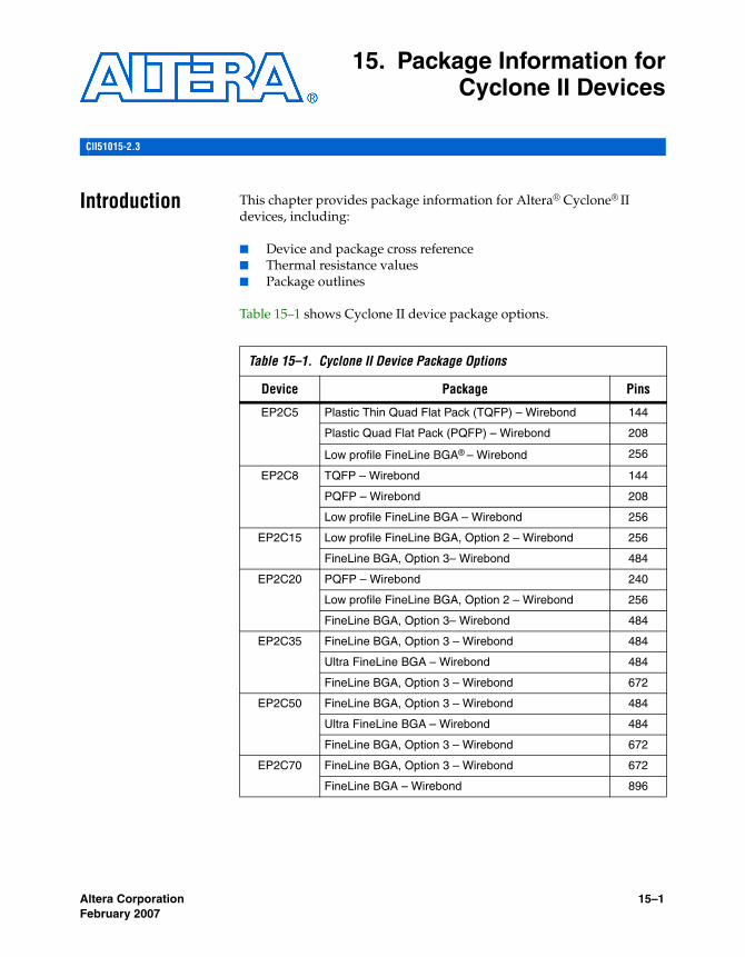
Altera Corporation 15–1 February 2007 15. Package Information for Cyclone II Devices Introduction This chapter provides package information for Altera ® Cyclone ® II devices, including: ■ Device and package cross reference ■ Thermal resistance values ■ Package outlines Table 15–1 shows Cyclone II device package options. Table 15–1. Cyclone II Device Package Options Device Package Pins EP2C5 Plastic Thin Quad Flat Pack (TQFP) – Wirebond 144 Plastic Quad Flat Pack (PQFP) – Wirebond 208 Low profile FineLine BGA ® – Wirebond 256 EP2C8 TQFP – Wirebond 144 PQFP – Wirebond 208 Low profile FineLine BGA – Wirebond 256 EP2C15 Low profile FineLine BGA, Option 2 – Wirebond 256 FineLine BGA, Option 3– Wirebond 484 EP2C20 PQFP – Wirebond 240 Low profile FineLine BGA, Option 2 – Wirebond 256 FineLine BGA, Option 3– Wirebond 484 EP2C35 FineLine BGA, Option 3 – Wirebond 484 Ultra FineLine BGA – Wirebond 484 FineLine BGA, Option 3 – Wirebond 672 EP2C50 FineLine BGA, Option 3 – Wirebond 484 Ultra FineLine BGA – Wirebond 484 FineLine BGA, Option 3 – Wirebond 672 EP2C70 FineLine BGA, Option 3 – Wirebond 672 FineLine BGA – Wirebond 896 CII51015-2.3
Transcript of Package Information for Cyclone II Devices
Altera Corporation February 2007
CII51015-2.3
15. Package Information forCyclone II Devices
Introduction This chapter provides package information for Altera® Cyclone® II devices, including:
■ Device and package cross reference■ Thermal resistance values■ Package outlines
Table 15–1 shows Cyclone II device package options.
Table 15–1. Cyclone II Device Package Options
Device Package Pins
EP2C5 Plastic Thin Quad Flat Pack (TQFP) – Wirebond 144
Plastic Quad Flat Pack (PQFP) – Wirebond 208
Low profile FineLine BGA® – Wirebond 256
EP2C8 TQFP – Wirebond 144
PQFP – Wirebond 208
Low profile FineLine BGA – Wirebond 256
EP2C15 Low profile FineLine BGA, Option 2 – Wirebond 256
FineLine BGA, Option 3– Wirebond 484
EP2C20 PQFP – Wirebond 240
Low profile FineLine BGA, Option 2 – Wirebond 256
FineLine BGA, Option 3– Wirebond 484
EP2C35 FineLine BGA, Option 3 – Wirebond 484
Ultra FineLine BGA – Wirebond 484
FineLine BGA, Option 3 – Wirebond 672
EP2C50 FineLine BGA, Option 3 – Wirebond 484
Ultra FineLine BGA – Wirebond 484
FineLine BGA, Option 3 – Wirebond 672
EP2C70 FineLine BGA, Option 3 – Wirebond 672
FineLine BGA – Wirebond 896
15–1
Thermal Resistance
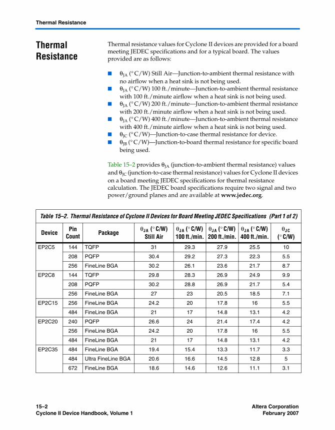
Thermal Resistance
Thermal resistance values for Cyclone II devices are provided for a board meeting JEDEC specifications and for a typical board. The values provided are as follows:
■ θJA (° C/W) Still Air—Junction-to-ambient thermal resistance with no airflow when a heat sink is not being used.
■ θJA (° C/W) 100 ft./minute—Junction-to-ambient thermal resistance with 100 ft./minute airflow when a heat sink is not being used.
■ θJA (° C/W) 200 ft./minute—Junction-to-ambient thermal resistance with 200 ft./minute airflow when a heat sink is not being used.
■ θJA (° C/W) 400 ft./minute—Junction-to-ambient thermal resistance with 400 ft./minute airflow when a heat sink is not being used.
■ θJC (° C/W)—Junction-to-case thermal resistance for device.■ θJB (° C/W)—Junction-to-board thermal resistance for specific board
being used.
Table 15–2 provides θJA (junction-to-ambient thermal resistance) values and θJC (junction-to-case thermal resistance) values for Cyclone II devices on a board meeting JEDEC specifications for thermal resistance calculation. The JEDEC board specifications require two signal and two power/ground planes and are available at www.jedec.org.
Table 15–2. Thermal Resistance of Cyclone II Devices for Board Meeting JEDEC Specifications (Part 1 of 2)
Device Pin Count Package
θJ A (° C/W) Still Air
θJ A (° C/W) 100 ft./min.
θJ A (° C/W) 200 ft./min.
θJ A (° C/W) 400 ft./min.
θJ C (° C/W)
EP2C5 144 TQFP 31 29.3 27.9 25.5 10
208 PQFP 30.4 29.2 27.3 22.3 5.5
256 FineLine BGA 30.2 26.1 23.6 21.7 8.7
EP2C8 144 TQFP 29.8 28.3 26.9 24.9 9.9
208 PQFP 30.2 28.8 26.9 21.7 5.4
256 FineLine BGA 27 23 20.5 18.5 7.1
EP2C15 256 FineLine BGA 24.2 20 17.8 16 5.5
484 FineLine BGA 21 17 14.8 13.1 4.2
EP2C20 240 PQFP 26.6 24 21.4 17.4 4.2
256 FineLine BGA 24.2 20 17.8 16 5.5
484 FineLine BGA 21 17 14.8 13.1 4.2
EP2C35 484 FineLine BGA 19.4 15.4 13.3 11.7 3.3
484 Ultra FineLine BGA 20.6 16.6 14.5 12.8 5
672 FineLine BGA 18.6 14.6 12.6 11.1 3.1
15–2 Altera CorporationCyclone II Device Handbook, Volume 1 February 2007
Package Information for Cyclone II Devices
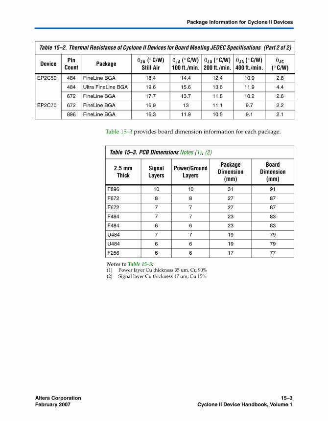
Table 15–3 provides board dimension information for each package.
EP2C50 484 FineLine BGA 18.4 14.4 12.4 10.9 2.8
484 Ultra FineLine BGA 19.6 15.6 13.6 11.9 4.4
672 FineLine BGA 17.7 13.7 11.8 10.2 2.6
EP2C70 672 FineLine BGA 16.9 13 11.1 9.7 2.2
896 FineLine BGA 16.3 11.9 10.5 9.1 2.1
Table 15–2. Thermal Resistance of Cyclone II Devices for Board Meeting JEDEC Specifications (Part 2 of 2)
Device Pin Count Package
θJ A (° C/W) Still Air
θJ A (° C/W) 100 ft./min.
θJ A (° C/W) 200 ft./min.
θJ A (° C/W) 400 ft./min.
θJ C (° C/W)
Table 15–3. PCB Dimensions Notes (1), (2)
2.5 mm Thick
Signal Layers
Power/Ground Layers
Package Dimension
(mm)
Board Dimension
(mm)
F896 10 10 31 91
F672 8 8 27 87
F672 7 7 27 87
F484 7 7 23 83
F484 6 6 23 83
U484 7 7 19 79
U484 6 6 19 79
F256 6 6 17 77
Notes to Table 15–3:(1) Power layer Cu thickness 35 um, Cu 90%(2) Signal layer Cu thickness 17 um, Cu 15%
Altera Corporation 15–3February 2007 Cyclone II Device Handbook, Volume 1
Package Outlines
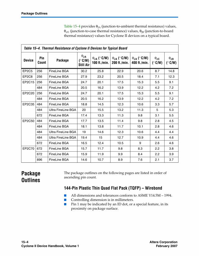
Table 15–4 provides θJA (junction-to-ambient thermal resistance) values, θJ C (junction-to-case thermal resistance) values, θJB (junction-to-board thermal resistance) values for Cyclone II devices on a typical board.
Package Outlines
The package outlines on the following pages are listed in order of ascending pin count.
144-Pin Plastic Thin Quad Flat Pack (TQFP) – Wirebond
■ All dimensions and tolerances conform to ASME Y14.5M – 1994.■ Controlling dimension is in millimeters.■ Pin 1 may be indicated by an ID dot, or a special feature, in its
proximity on package surface.
Table 15–4. Thermal Resistance of Cyclone II Devices for Typical Board
Device Pin Count Package
θJ A (° C/W) Still Air
θJ A (° C/W) 100 ft./min.
θJ A (° C/W) 200 ft./min.
θJ A (° C/W) 400 ft./min.
θJ C (° C/W)
θJ B (° C/W)
EP2C5 256 FineLine BGA 30.2 25.8 22.9 20.6 8.7 14.8
EP2C8 256 FineLine BGA 27.9 23.2 20.5 18.4 7.1 12.3
EP2C15 256 FineLine BGA 24.7 20.1 17.5 15.3 5.5 9.1
484 FineLine BGA 20.5 16.2 13.9 12.2 4.2 7.2
EP2C20 256 FineLine BGA 24.7 20.1 17.5 15.3 5.5 9.1
484 FineLine BGA 20.5 16.2 13.9 12.2 4.2 7.2
EP2C35 484 FineLine BGA 18.8 14.5 12.3 10.6 3.3 5.7
484 Ultra FineLine BGA 20 15.5 13.2 11.3 5 5.3
672 FineLine BGA 17.4 13.3 11.3 9.8 3.1 5.5
EP2C50 484 FineLine BGA 17.7 13.5 11.4 9.8 2.8 4.5
484 FineLine BGA 18.1 13.8 11.7 10.1 2.8 4.6
484 Ultra FineLine BGA 19 14.6 12.3 10.6 4.4 4.4
484 Ultra FineLine BGA 19.4 15 12.7 10.9 4.4 4.6
672 FineLine BGA 16.5 12.4 10.5 9 2.6 4.6
EP2C70 672 FineLine BGA 15.7 11.7 9.8 8.3 2.2 3.8
672 FineLine BGA 15.9 11.9 9.9 8.4 2.2 3.9
896 FineLine BGA 14.6 10.7 8.9 7.6 2.1 3.7
15–4 Altera CorporationCyclone II Device Handbook, Volume 1 February 2007
Package Information for Cyclone II Devices
Tables 15–5 and 15–6 show the package information and package outline figure references, respectively, for the 144-pin TQFP package.
Table 15–5. 144-Pin TQFP Package Information
Description Specification
Ordering code reference T
Package acronym TQFP
Lead frame material Copper
Lead finish (plating) Regular: 85Sn:15Pb (Typ.)Pb-free: Matte Sn
JEDEC Outline Reference MS-026 Variation: BFB
Maximum lead coplanarity 0.003 inches (0.08mm)
Weight 1.3 g
Moisture sensitivity level Printed on moisture barrier bag
Table 15–6. 144-Pin TQFP Package Outline Dimensions
SymbolMillimeter
Min. Nom. Max.
A – – 1.60
A1 0.05 – 0.15
A2 1.35 1.40 1.45
D 22.00 BSC
D1 20.00 BSC
E 22.00 BSC
E1 20.00 BSC
L 0.45 0.60 0.75
L1 1.00 REF
S 0.20 – –
b 0.17 0.22 0.27
c 0.09 – 0.20
e 0.50 BSC
θ 0° 3.5° 7°
Altera Corporation 15–5February 2007 Cyclone II Device Handbook, Volume 1
Package Outlines
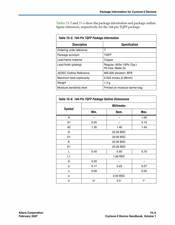
Figure 15–1 shows a 144-pin TQFP package outline.
Figure 15–1. 144-Pin TQFP Package Outline
Pin 1 ID
EE1
D1
D
Pin 144
S
L
L1
DETAIL A
Gage Plane
0.25mm
C
b
e
See Detail A
Pin 1
AA2
A1
Pin 36
15–6 Altera CorporationCyclone II Device Handbook, Volume 1 February 2007

Package Information for Cyclone II Devices
208-Pin Plastic Quad Flat Pack (PQFP) – Wirebond
■ All dimensions and tolerances conform to ASME Y14.5M - 1994.■ Controlling dimension is in millimeters.■ Pin 1 may be indicated by an ID dot in its proximity on package
surface.
Tables 15–7 and 15–8 show the package information and package outline figure references, respectively, for the 208-pin PQFP package.
Table 15–7. 208-Pin PQFP Package Information
Description Specification
Ordering code reference Q
Package acronym PQFP
Lead material Copper
Lead finish (plating) Regular: 85Sn:15Pb (Typ.)Pb-free: Matte Sn
JEDEC Outline Reference MS-029 Variation: FA-1
Maximum lead coplanarity 0.003 inches (0.08 mm)
Weight 5.7 g
Moisture sensitivity level Printed on moisture barrier bag
Table 15–8. 208-Pin PQFP Package Outline Dimensions (Part 1 of 2)
SymbolMillimeter
Min. Nom. Max.
A – – 4.10
A1 0.25 – 0.50
A2 3.20 3.40 3.60
D 30.60 BSC
D1 28.00 BSC
E 30.60 BSC
E1 28.00 BSC
L 0.50 0.60 0.75
L1 1.30 REF
S 0.20 – –
b 0.17 – 0.27
c 0.09 – 0.20
Altera Corporation 15–7February 2007 Cyclone II Device Handbook, Volume 1
Package Outlines
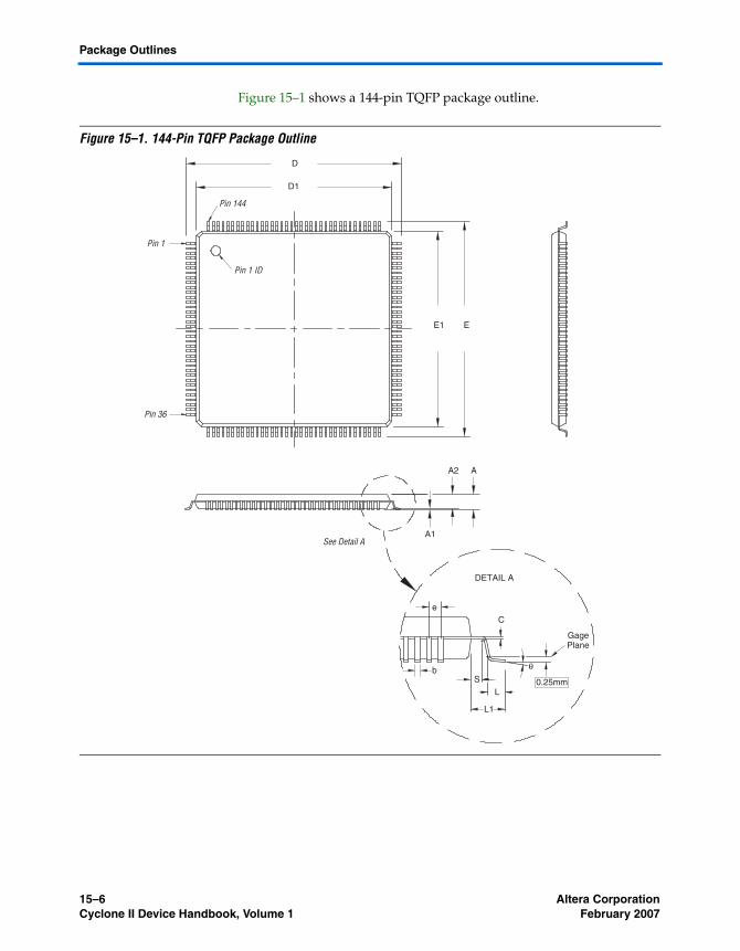
Figure 15–2 shows a 208-pin PQFP package outline.
Figure 15–2. 208-pin PQFP Package Outline
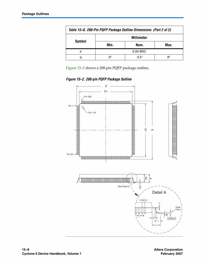
e 0.50 BSC
q 0° 3.5° 8°
Table 15–8. 208-Pin PQFP Package Outline Dimensions (Part 2 of 2)
SymbolMillimeter
Min. Nom. Max.
Pin 1 ID
E
D1
D
Pin 208
AA2
A1
S
L
L1
Detail A
GagePlane
0.25mm
C
b
e
See Detail A
E1
Pin 1
Pin 52
15–8 Altera CorporationCyclone II Device Handbook, Volume 1 February 2007
Package Information for Cyclone II Devices
240-Pin Plastic Quad Flat Pack (PQFP)
■ All dimensions and tolerances conform to ASME Y14.5M – 1994.■ Controlling dimension is in millimeters.■ Pin 1 may be indicated by an ID dot, or a special feature, in its
proximity on package surface.
Tables 15–9 and 15–10 show the package information and package outline figure references, respectively, for the 240-pin PQFP package.
Table 15–9. 240-Pin PQFP Package Information
Description Specification
Ordering Code Reference Q
Package Acronym PQFP
Leadframe Material Copper
Lead Finish (Plating) Regular: 85Sn:15Pb (Typ.)Pb-free: Matte Sn
JEDEC Outline Reference MS-029 Variation: GA
Maximum Lead Coplanarity 0.003 inches (0.08mm)
Weight 7.0 g
Moisture Sensitivity Level Printed on moisture barrier bag
Table 15–10. 240-Pin PQFP Package Outline Dimensions (Part 1 of 2)
SymbolMillimeter
Min. Nom. Max.
A – – 4.10
A1 0.25 – 0.50
A2 3.20 3.40 3.60
D 34.60 BSC
D1 32.00 BSC
E 34.60 BSC
E1 32.00 BSC
L 0.45 0.60 0.75
L1 1.30 REF
S 0.20 – –
b 0.17 – 0.27
c 0.09 – 0.20
Altera Corporation 15–9February 2007 Cyclone II Device Handbook, Volume 1
Package Outlines
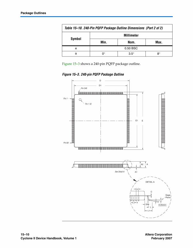
Figure 15–3 shows a 240-pin PQFP package outline.
Figure 15–3. 240-pin PQFP Package Outline
e 0.50 BSC
θ 0° 3.5° 8°
Table 15–10. 240-Pin PQFP Package Outline Dimensions (Part 2 of 2)
SymbolMillimeter
Min. Nom. Max.
SL
L1
DETAIL A
GagePlane
0.25mm
C
b
e
See Detail A
D
D1
EE1
A2 A
A1
Pin 1 ID
Pin 1
Pin 60
Pin 240
15–10 Altera CorporationCyclone II Device Handbook, Volume 1 February 2007

Package Information for Cyclone II Devices
256-Pin FineLine Ball-Grid Array, Option 2 – Wirebond
■ All dimensions and tolerances conform to ASME Y14.5M - 1994.■ Controlling dimension is in millimeters.■ Pin A1 may be indicated by an ID dot, or a special feature, in its
proximity on the package surface.
1 This POD is applicable to the F256 package of the Cyclone II product only.
Tables 15–11 and 15–12 show the package information and package outline figure references, respectively, for the 256-pin FineLine BGA package.
Table 15–11. 256-Pin FineLine BGA Package Information
Description Specification
Ordering code reference F
Package acronym FineLine BGA
Substrate material BT
Solder ball composition Regular: 63Sn:37Pb (Typ.)Pb-free: Sn:3Ag:0.5Cu (Typ.)
JEDEC Outline Reference MO-192 Variation: AAF-1
Maximum lead coplanarity 0.008 inches (0.20 mm)
Weight 1.9 g
Moisture sensitivity level Printed on moisture barrier bag
Table 15–12. 256-Pin FineLine BGA Package Outline Dimensions
SymbolMillimeter
Min. Nom. Max.
A – – 1.55
A1 0.25 – –
A2 1.05 REF
A3 – – 0.80
D 17.00 BSC
E 17.00 BSC
b 0.40 0.50 0.55
e 1.00 BSC
Altera Corporation 15–11February 2007 Cyclone II Device Handbook, Volume 1
Package Outlines
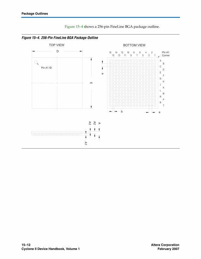
Figure 15–4 shows a 256-pin FineLine BGA package outline.
Figure 15–4. 256-Pin FineLine BGA Package Outline
D
E
Pin A1 ID
b e
e
A3
A1
A2 A
Pin A1
Corner
BOTTOM VIEWTOP VIEW
15–12 Altera CorporationCyclone II Device Handbook, Volume 1 February 2007
Package Information for Cyclone II Devices
484-Pin FineLine BGA, Option 3 – Wirebond
■ All dimensions and tolerances conform to ASME Y14.5M – 1994.■ Controlling dimension is in millimeters.■ Pin A1 may be indicated by an ID dot, or a special feature, in its
proximity on package surface.
Tables 15–13 and 15–14 show the package information and package outline figure references, respectively, for the 484-pin FineLine BGA package.
Table 15–13. 484-Pin FineLine BGA Package Information
Description Specification
Ordering code reference F
Package acronym FineLine BGA
Substrate material BT
Solder ball composition Regular: 63Sn:37Pb (Typ.) Pb-free: Sn:3Ag:0.5Cu (Typ.)
JEDEC Outline Reference MS-034 Variation: AAJ-1
Maximum lead coplanarity 0.008 inches (0.20 mm)
Weight 5.7 g
Moisture sensitivity level Printed on moisture barrier bag
Table 15–14. 484-Pin FineLine BGA Package Outline Dimensions
SymbolMillimeter
Min. Nom. Max.
A – – 2.60
A1 0.30 – –
A2 – – 2.20
A3 – – 1.80
D 23.00 BSC
E 23.00 BSC
b 0.50 0.60 0.70
e 1.00 BSC
Altera Corporation 15–13February 2007 Cyclone II Device Handbook, Volume 1
Package Outlines
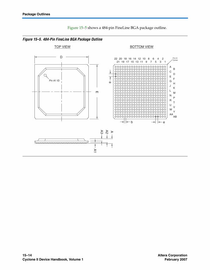
Figure 15–5 shows a 484-pin FineLine BGA package outline.
Figure 15–5. 484-Pin FineLine BGA Package Outline
D
E
Pin A1 ID
b e
A1
A2
Pin A1 Corner
A
VU
RT
P
L
NM
KJ
2
F
HG
ED
AB
C
1
A3
TOP VIEW BOTTOM VIEW
AAAB
YW
34
56
78
910
1112
1314
1516
1718
1920
2122
e
15–14 Altera CorporationCyclone II Device Handbook, Volume 1 February 2007
Package Information for Cyclone II Devices
484-Pin Ultra FineLine BGA – Wirebond
■ All dimensions and tolerances conform to ASME Y14.5M – 1994.■ Controlling dimension is in millimeters.■ Pin A1 may be indicated by an ID dot, or a special feature, in its
proximity on package surface.
Tables 15–15 and 15–16 show the package information and package outline figure references, respectively, for the 484-pin Ultra FineLine BGA package.
Table 15–15. 484-Pin Ultra FineLine BGA Package Information
Description Specification
Ordering Code Reference U
Package Acronym UBGA
Substrate Material BT
Solder Ball Composition Regular: 63Sn:37Pb (Typ.)Pb-free: Sn:3Ag:0.5Cu (Typ.)
JEDEC Outline Reference MO-216 Variation: BAP-2
Maximum Lead Coplanarity 0.005 inches (0.12mm)
Weight 1.8 g
Moisture Sensitivity Level Printed on moisture barrier bag
Table 15–16. 484-Pin Ultra FineLine BGA Package Outline Dimensions
SymbolMillimeter
Min. Nom. Max.
A – – 2.20
A1 0.20 – –
A2 0.65 – –
A3 0.80 TYP
D 19.00 BSC
E 19.00 BSC
b 0.40 0.50 0.60
e 0.80 BSC
Altera Corporation 15–15February 2007 Cyclone II Device Handbook, Volume 1
Package Outlines
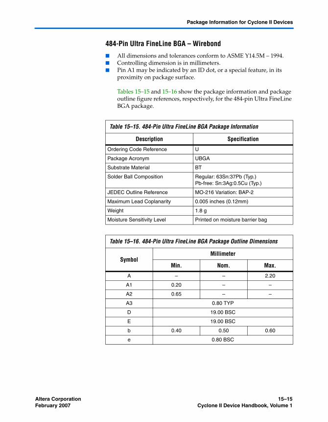
Figure 15–6 shows a 484-pin Ultra FineLine BGA package outline.
Figure 15–6. 484-Pin Ultra FineLine BGA Package Outline
BOTTOM VIEWTOP VIEW
D
E
Pin A1 ID
b
A3
A1
A2 A
Pin A1
Corner
e
e
15–16 Altera CorporationCyclone II Device Handbook, Volume 1 February 2007
Package Information for Cyclone II Devices
672-Pin FineLine BGA Package, Option 3 – Wirebond
■ All dimensions and tolerances conform to ASME Y14.5M - 1994.■ Controlling dimension is in millimeters.■ Pin A1 may be indicated by an ID dot, or a special feature, in its
proximity on the package surface.
Tables 15–17 and 15–18 show the package information and package outline figure references, respectively, for the 672-pin FineLine BGA package.
Table 15–17. 672-Pin FineLine BGA Package Information
Description Specification
Ordering code reference F
Package acronym FineLine BGA
Substrate material BT
Solder ball composition Regular: 63Sn:37Pb (Typ.)Pb-free: Sn:3Ag:0.5Cu (Typ.)
JEDEC Outline Reference MS-034 Variation: AAL-1
Maximum lead coplanarity 0.008 inches (0.20 mm)
Weight 7.7 g
Moisture sensitivity level Printed on moisture barrier bag
Table 15–18. 672-Pin FineLine BGA Package Outline Dimensions
SymbolDimensions (mm)
Min. Nom. Max.
A – – 2.60
A1 0.30 – –
A2 – – 2.20
A3 – – 1.80
D 27.00 BSC
E 27.00 BSC
b 0.50 0.60 0.70
e 1.00 BSC
Altera Corporation 15–17February 2007 Cyclone II Device Handbook, Volume 1
Package Outlines
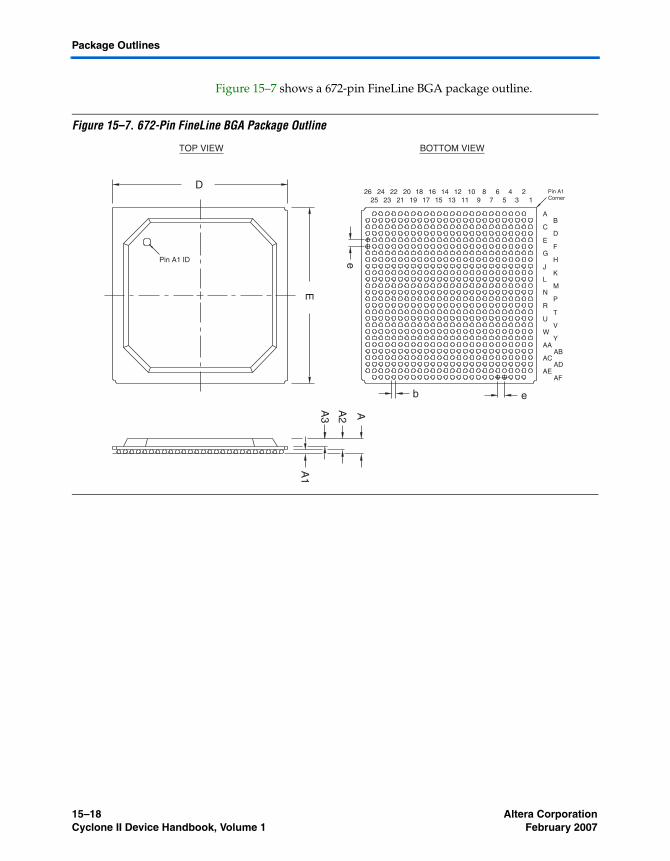
Figure 15–7 shows a 672-pin FineLine BGA package outline.
Figure 15–7. 672-Pin FineLine BGA Package Outline
67
89
1011
1213
1415
1617
1819
2021
22
e
D
E
Pin A1 ID
b e
A1
A2
Pin A1 Corner
A
VU
RT
P
L
NM
KJ
2
F
HG
ED
AB
C
1
AAAB
YW
34
525 2326 24
AEAF
ACAD
A3
BOTTOM VIEWTOP VIEW
15–18 Altera CorporationCyclone II Device Handbook, Volume 1 February 2007
Package Information for Cyclone II Devices
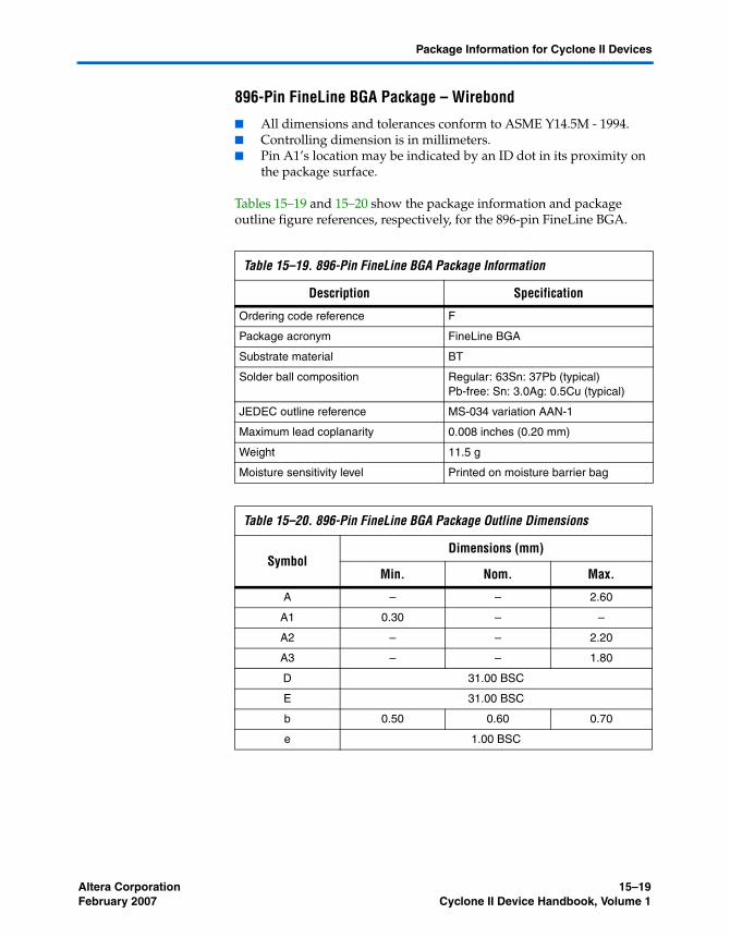
896-Pin FineLine BGA Package – Wirebond
■ All dimensions and tolerances conform to ASME Y14.5M - 1994.■ Controlling dimension is in millimeters.■ Pin A1’s location may be indicated by an ID dot in its proximity on
the package surface.
Tables 15–19 and 15–20 show the package information and package outline figure references, respectively, for the 896-pin FineLine BGA.
Table 15–19. 896-Pin FineLine BGA Package Information
Description Specification
Ordering code reference F
Package acronym FineLine BGA
Substrate material BT
Solder ball composition Regular: 63Sn: 37Pb (typical)Pb-free: Sn: 3.0Ag: 0.5Cu (typical)
JEDEC outline reference MS-034 variation AAN-1
Maximum lead coplanarity 0.008 inches (0.20 mm)
Weight 11.5 g
Moisture sensitivity level Printed on moisture barrier bag
Table 15–20. 896-Pin FineLine BGA Package Outline Dimensions
SymbolDimensions (mm)
Min. Nom. Max.
A – – 2.60
A1 0.30 – –
A2 – – 2.20
A3 – – 1.80
D 31.00 BSC
E 31.00 BSC
b 0.50 0.60 0.70
e 1.00 BSC
Altera Corporation 15–19February 2007 Cyclone II Device Handbook, Volume 1
Package Outlines
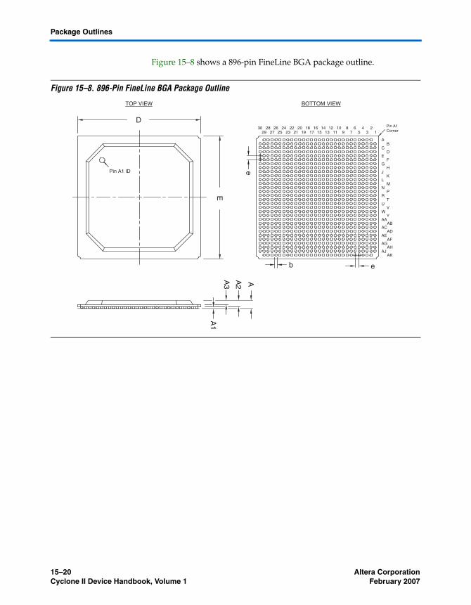
Figure 15–8 shows a 896-pin FineLine BGA package outline.
Figure 15–8. 896-Pin FineLine BGA Package Outline
25 2326 24
AEAF
ACAD
272930 28
AG
AKAJ
AHA
3
BOTTOM VIEWTOP VIEW
67
89
1011
1213
1415
1617
1819
2021
22
e
D
E
Pin A1 ID
b eA
1
A2
Pin A1 Corner
A
VU
RT
P
L
NM
KJ
2
F
HG
ED
AB
C
1
AAAB
YW
34
5
15–20 Altera CorporationCyclone II Device Handbook, Volume 1 February 2007
Package Information for Cyclone II Devices
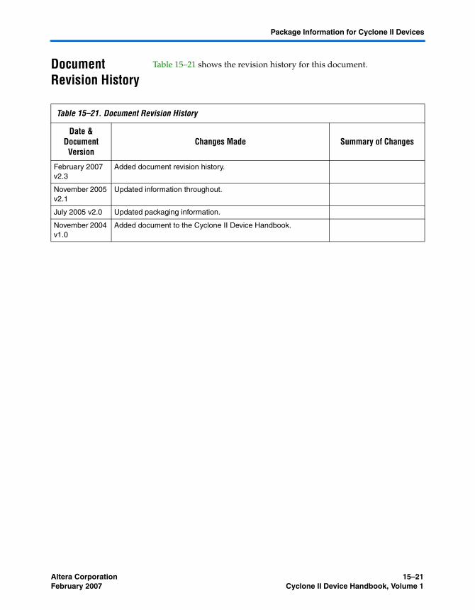
Document Revision History
Table 15–21 shows the revision history for this document.
Table 15–21. Document Revision History
Date & Document
VersionChanges Made Summary of Changes
February 2007 v2.3
Added document revision history.
November 2005 v2.1
Updated information throughout.
July 2005 v2.0 Updated packaging information.
November 2004 v1.0
Added document to the Cyclone II Device Handbook.
Altera Corporation 15–21February 2007 Cyclone II Device Handbook, Volume 1

Document Revision History
15–22 Altera CorporationCyclone II Device Handbook, Volume 1 February 2007