PA99 • PA99A - apexanalog.com • PA99A FEATURES ... 9 TEMPB The cathode for the temperature...
12
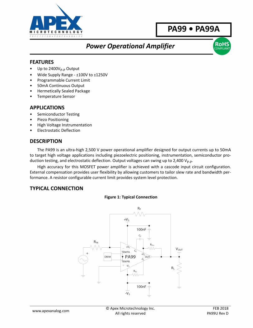
www.apexanalog.com © Apex Microtechnology Inc. All rights reserved FEB 2018 PA99U Rev D Power Operational Amplifier RoHS COMPLIANT PA99 • PA99A FEATURES • Up to 2400V P-P Output • Wide Supply Range - ±100V to ±1250V • Programmable Current Limit • 50mA Continuous Output • Hermetically Sealed Package • Temperature Sensor APPLICATIONS • Semiconductor Testing • Piezo Positioning • High Voltage Instrumentation • Electrostatic Deflection DESCRIPTION The PA99 is an ultra-high 2,500 V power operational amplifier designed for output currents up to 50mA to target high voltage applications including piezoelectric positioning, instrumentation, semiconductor pro- duction testing, and electrostatic deflection. Output voltages can swing up to 2,400 V P-P . High accuracy for this MOSFET power amplifier is achieved with a cascode input circuit configuration. External compensation provides user flexibility by allowing customers to tailor slew rate and bandwidth per- formance. A resistor configurable current limit provides system level protection. TYPICAL CONNECTION Figure 1: Typical Connection R F R L + R IN V OUT +VS +CL -CL PA99 OUT CC -VS 100nF +V S RCL- 100nF -V S RCL+ CC DMM TEMPA TEMPB
Transcript of PA99 • PA99A - apexanalog.com • PA99A FEATURES ... 9 TEMPB The cathode for the temperature...
www.apexanalog.com© Apex Microtechnology Inc
All rights reserved
Power Operational Am
PA99 • PA99A
plifier RoHSCOMPLIANT
FEATURES• Up to 2400VP-P Output
• Wide Supply Range - ±100V to ±1250V• Programmable Current Limit• 50mA Continuous Output• Hermetically Sealed Package• Temperature Sensor
APPLICATIONS• Semiconductor Testing• Piezo Positioning• High Voltage Instrumentation• Electrostatic Deflection
DESCRIPTION
The PA99 is an ultra-high 2,500 V power operational amplifier designed for output currents up to 50mAto target high voltage applications including piezoelectric positioning, instrumentation, semiconductor pro-duction testing, and electrostatic deflection. Output voltages can swing up to 2,400 VP-P.
High accuracy for this MOSFET power amplifier is achieved with a cascode input circuit configuration.External compensation provides user flexibility by allowing customers to tailor slew rate and bandwidth per-formance. A resistor configurable current limit provides system level protection.
TYPICAL CONNECTION
Figure 1: Typical Connection
RF
RL
+
RIN
VOUT+VS
+CL
-CLPA99 OUT
CC
-VS
100nF
+VS
RCL-
100nF
-VS
RCL+
CC
DMM
TEMPA
TEMPB
. FEB 2018PA99U Rev D

PA99 • PA99A
PINOUT AND DESCRIPTION TABLE
Figure 2: External Connections
Pin Number Name Description
1, 2 NC No connection.
3 -CL Connect a negative current limit resistor between this pin and -Vs pin.
4 -Vs The negative supply rail.
5 CCConnect a compensation capacitor between this pin and +CL pin. The compensation
capacitor needs to be rated for at least the maximum supply voltage.
6 +CLConnect a positive current limit resistor between this pin and the OUT pin. Output
current flows out of this pin through RCL+.
7 OUT The output. Connect this pin to load and to the feedback resistors.
8 TEMPA The anode for the temperature sensing diode.
9 TEMPB The cathode for the temperature sensing diode.
10 +Vs The positive supply rail.
11 -IN The inverting input.
12 +IN The non-inverting input.
2 PA99U Rev D

PA99 • PA99A
SPECIFICATIONS
Unless noted otherwise, the test conditions are as follows: TC = 25°C, VS = 2000V, RL = 50 kΩ, AV = 100, RF =
200 kΩ, CC=15pF. DC input specifications are value given. The power supply voltage is typical rating.
ABSOLUTE MAXIMUM RATINGS
INPUT
ParameterPA99 & PA99A
UnitSymbol Min Max
Supply Voltage +Vs to -Vs 2500 V
Output Current, Peak, within SOA IO ±70 mA
Power Dissipation, internal, DC PD 37 W
Input Voltage, common mode Vcm -VS+50 to +VS-50 V
Input Voltage, differential VIN (Diff) ±20 V
Temperature, pin solder, 10s +225 °C
Temperature, junction1
1. Long term operation at the maximum junction temperature will result in reduced product life. Derate internal power dissipation to achieve high MTTF.
TJ +150 °C
Temperature, storage -40 +150 °C
Operating Temperature Range, case TC -40 +85 °C
Parameter Test ConditionsPA99 PA99A
UnitMin Typ Max Min Typ Max
Offset Voltage, initial 2.0 5.0 2.0 mV
Offset Voltage vs. temperature Full temp range 75 50 µV/°C
Offset Voltage vs. supply 0.1 * µV/V
Bias Current, Initial1
1. Doubles for every 10°C of case temperature increase.
50 * pA
Bias Current vs. supply 0.01 * pA/V
Offset Current, Initial 5.0 50 * * pA
Input Resistance, DC 1011 * Ω
Input Capacitance 13 * pF
Common Mode Voltage Range-Vs + 50+Vs - 50
* V
Common Mode Rejection, DC 134 * dB
Input Noise20 kHz BW, RS=10 kΩ
2 * µV RMS
PA99U Rev D 3

PA99 • PA99A
GAIN
OUTPUT
POWER SUPPLY
THERMAL
Note: An asterisk (*) in a specification column of PA99A indicates that the value is identical to the specifica-tion for the PA99 in the applicable column to the left
Parameter Test ConditionsPA99 PA99A
UnitMin Typ Max Min Typ Max
Open Loop, @ 15 Hz 117 * dB
Gain Bandwidth Product AV=100, 280 kHz 28 * MHz
Power BandwidthVO = 2000V,
VS = 2200V1.6 5 * * kHz
Phase Margin 60 * °
Harmonic Distortion, HD2 1 kHz 61 * dB
Harmonic Distortion, HD3 1 kHz 56 * dB
Parameter Test ConditionsPA99 PA99A
UnitMin Typ Max Min Typ Max
Voltage Swing, negative rail I O = 20mA -Vs+20 * V
Voltage Swing, positive rail I O = 20mA +Vs-20 * V
Current, continuous Within SOA ±50 * mA
Slew Rate, rising 10 30 * * V/µs
Slew Rate, falling 10 30 * * V/µs
Resistive Load 1000 * Ω
Parameter Test ConditionsPA99 PA99A
UnitMin Typ Max Min Typ Max
Voltage ±100 ±1250 * * V
Current, quiescent 4.0 * mA
Parameter Test ConditionsPA99 PA99A
UnitMin Typ Max Min Typ Max
Resistance, DC, junction to caseFull temp range, F < 60 Hz
3.3 * °C/W
Resistance, junction to air Full temp range 15.4 * °C/W
4 PA99U Rev D

PA99 • PA99A
TYPICAL PERFORMANCE GRAPHS
Figure 3: Power Derating Figure 4: Large Signal Pulse Response
Figure 5: Small Signal Pulse Response Figure 6: Large Signal Response with Current Limit
40
35
30
25
20
15
10
5
00 25 50 10075
Case Temperature, TC (°C)
PA99U Rev D 5

PA99 • PA99A
Figure 7: Open Loop Gain vs. Frequency Figure 8: Phase Response
Figure 9: Common Mode Rejection vs. Frequency
Figure 10: Power Supply Rejection
160
140
120
100
80
60
40
20
01 10 100 1k 10k 1M100k
Frequency (Hz)
Ope
n Lo
op G
ain (d
B)
10M
Cc=15pF
0
-20
-40
-60
-100
-140
-160
-180
-2001 10 1k 10k 100k 100M10M
Frequency (Hz)
Phas
e, (°
)
-80
-120
1M100
Cc=15pF
6 PA99U Rev D

PA99 • PA99A
Figure 11: Quiescent Current Figure 12: Output Voltage Swing
Figure 13: Input Noise vs. Frequency Figure 14: Negative Current Limit Resistor
20
19
18
17
16
15
14
130 20k 40k 60k 80k 120k100k
Frequency (Hz)
Inpu
t Noi
se E
N, (
nV/
√H
z)
Vs = +/- 1100V
AV = -100
N
PA99U Rev D 7
PA99 • PA99A
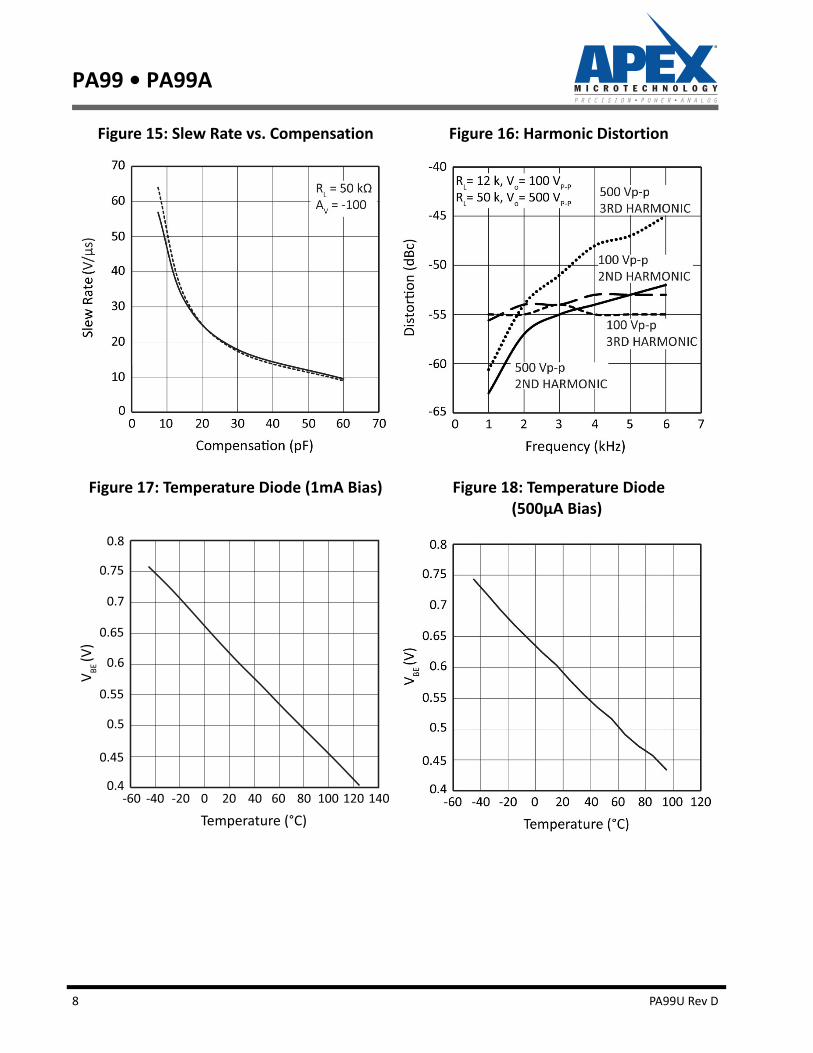
Figure 15: Slew Rate vs. Compensation Figure 16: Harmonic Distortion
Figure 17: Temperature Diode (1mA Bias) Figure 18: Temperature Diode (500µA Bias)
0.8
0.75
0.7
0.65
0.6
0.55
0.5
0.45
0.40-20 20 40 100 140120
Temperature (°C)
V BE (V
)
60 80-40-60
8 PA99U Rev D

PA99 • PA99A
SAFE OPERATING AREA (SOA)
Figure 19: SOA
VS - VO (V)
S
10
1100
TC = 25°C
TC = 85°C
PA99U Rev D 9

PA99 • PA99A
GENERAL
Please read Application Note 1 “General Operating Considerations” which covers stability, supplies, heatsinking, mounting, current limit, SOA interpretation, and specification interpretation. Visit www.apexana-log.com for Apex Microtechnology’s complete Application Notes library, Technical Seminar Workbook, andEvaluation Kits.
TYPICAL APPLICATION
Figure 20: Typical Application Circuit
Figure 20 shows PA99 in a typical inverting amplifier circuit. The resistors RLIM+ and RLIM- are used to limit
the current output. If no current limit is desired, a direct connection between CL+ and OUT is required for
proper operation, and CL- must be connected to -VS with a resistor larger or equal 200 k in that case.
OUTPUT CURRENT AND DEVICE COOLING
PA99 can handle output currents of ±50mA, but careful considerations need to be done about propercooling of the device to avoid damage due to overheating. When calculating the power loss inside the device,the output current and the quiescent currents need to be considered.
For example, if the device uses a supply voltage of 1000V, the output voltage to a resistive load is 500Vand the output current is 50mA, the power loss inside the device is calculated as follows:
In the above example, the device will dissipate 27W of heat. If we supply 1500V instead of 1000V, thepower dissipation of the device doubles, resulting in a loss of 54W.
As alternative to extensive device cooling, it should be considered to alter the supply voltage of thedevice. If the PA99 is used in a test environment where is needs to drive 50mA at 500V but 5mA at 2000V,consider supplying two voltages, i.e. 1000V and 2500V, and provide for sufficient cooling for the approximate30W of power dissipation of the device.
PDEVICE 1000V 500V– 50 4+ mA 27W==
10 PA99U Rev D

PA99 • PA99A
OVERVOLTAGE PROTECTION
Although the PA99 can withstand differential input voltages up to ±20V, additional external protection isrecommended. In most applications 1N4148 signal diodes connected anti-parallel across the input pins aresufficient. In more demanding applications where bias current is important diode connected JFETs such as2N4416 will be required. In either case the differential input voltage will be clamped to ±0.7V. This is usuallysufficient overdrive to produce the maximum power bandwidth.
CURRENT LIMIT
PA99 allows independent setting of a positive and negative current limit.
POSITIVE CURRENT LIMIT
The resistor value RLIM+ for positive current limit is calculated as follows:
NEGATIVE CURRENT LIMIT
The current limit resistor for the negative current limit can be approximated as:
TEMPERATURE SENSING
The temperature sensing pins of the PA99 are connected to a 1N4448 type of diode that can be used tosense the temperature inside the device. A typical application will use a current source as the best means forthe excitation of the diode.
Positive Current Limit Measured Resistor Value (RLIM+)
5mA 130 Ω10mA 68 Ω20mA 32.4 Ω40mA 15.8 Ω
Negative Current Limit Measured Resistor Value (RLIM-)
5mA 8 kΩ10mA 15 kΩ20mA 33 kΩ40mA 92 kΩ
RLIM 0.65VILIM A -------------------=
RLIM 5324 e76.4 ILIM
A =
PA99U Rev D 11

PA99 • PA99A
PACKAGE OPTIONS
PACKAGE STYLE CW
Part Number Apex Package Style Description
PA99 CW 12-pin Power DIP, High Voltage
PA99A CW 12-pin Power DIP, High Voltage
1
2
3
4
5
6
12
11
10
9
8
7
2.935±0.05
.115R
1.605±0.05
.0200.220±0.05
3.6693.300
2.969±0.01
0.400±0.002TYP
0.025±0.002
12 PA99U Rev D
NEED TECHNICAL HELP? CONTACT APEX SUPPORT! For all Apex Microtechnology product questions and inquiries, call toll free 800-546-2739 in North America. Forinquiries via email, please contact [email protected]. International customers can also requestsupport by contacting their local Apex Microtechnology Sales Representative. To find the one nearest to you,go to www.apexanalog.com
IMPORTANT NOTICE
Apex Microtechnology, Inc. has made every effort to insure the accuracy of the content contained in this document. However, the information is
subject to change without notice and is provided "AS IS" without warranty of any kind (expressed or implied). Apex Microtechnology reserves the right
to make changes without further notice to any specifications or products mentioned herein to improve reliability. This document is the property ofApex Microtechnology and by furnishing this information, Apex Microtechnology grants no license, expressed or implied under any patents, mask
work rights, copyrights, trademarks, trade secrets or other intellectual property rights. Apex Microtechnology owns the copyrights associated with the
information contained herein and gives consent for copies to be made of the information only for use within your organization with respect to ApexMicrotechnology integrated circuits or other products of Apex Microtechnology. This consent does not extend to other copying such as copying for
general distribution, advertising or promotional purposes, or for creating any work for resale.
APEX MICROTECHNOLOGY PRODUCTS ARE NOT DESIGNED, AUTHORIZED OR WARRANTED TO BE SUITABLE FOR USE IN PRODUCTS USED FOR LIFESUPPORT, AUTOMOTIVE SAFETY, SECURITY DEVICES, OR OTHER CRITICAL APPLICATIONS. PRODUCTS IN SUCH APPLICATIONS ARE UNDERSTOOD TO BE
FULLY AT THE CUSTOMER OR THE CUSTOMER’S RISK.
Apex Microtechnology, Apex and Apex Precision Power are trademarks of Apex Microtechnology, Inc. All other corporate names noted herein may betrademarks of their respective holders.