PA94 Capacitance 4 pF ... Gain Bandwidth Product @ 1 MHzRL = 5 kΩ 140 MHz Power Bandwidth RL = 5...
13
www.apexanalog.com © Apex Microtechnology Inc. All rights reserved Sep 2017 PA94U Rev Q High Voltage Power Operational Amplifiers RoHS COMPLIANT PA94 FEATURES • High Voltage— 900V (±450V) • High Slew Rate — 500V/µs • Output Current— 100mA • Programmable Current Limit APPLICATIONS • High Voltage Instrumentation • Programmable Power Supplies up to ±430V • Mass Spectrometers • Semiconductor Measurement Equipment DESCRIPTION The PA94 is a high voltage, MOSFET operational amplifier designed as a low cost solution for driving con‐ tinuous output currents up to 100mA and pulse currents up to 200mA into capacitive loads. The safe operat‐ ing area (SOA) has no second breakdown limitations and can be observed for all load types by choosing an appropriate current limiting resistor. The MOSFET output stage is biased AB for linear operation. External compensation provides flexibility in choosing bandwidth and slew rate for the application. Apex Microtech‐ nology’s Power SIP uses a minimum of board space allowing for high density circuit boards. The Power SIP is electrically isolated. Isolating thermal washers (TW13) prevent arcing from pins to heatsink. Figure 1: Equivalent Schematic Q1 Q2 R1A R1B C2 R3 Q3 CC1 CC2 Q6 Q5 R9 R11 R12 Q29 R20 R27 Q30 Q29 Q8 R4 R7 Q4 ILIM OUT Q14 R19 Q21 Q11 +V S –IN +IN –V S R10 Q15A Q15B 4 6 7 8 10 2 1 12
Transcript of PA94 Capacitance 4 pF ... Gain Bandwidth Product @ 1 MHzRL = 5 kΩ 140 MHz Power Bandwidth RL = 5...

www.apexanalog.com© Apex Microtechnology Inc
All rights reserved
High Voltage Power Operatio
PA94
nal Amplifiers RoHSCOMPLIANT
FEATURES
• High Voltage— 900V (±450V)• High Slew Rate — 500V/µs• Output Current— 100mA• Programmable Current Limit
APPLICATIONS
• High Voltage Instrumentation• Programmable Power Supplies up to ±430V• Mass Spectrometers• Semiconductor Measurement Equipment
DESCRIPTION
The PA94 is a high voltage, MOSFET operational amplifier designed as a low cost solution for driving con‐tinuous output currents up to 100mA and pulse currents up to 200mA into capacitive loads. The safe operat‐ing area (SOA) has no second breakdown limitations and can be observed for all load types by choosing anappropriate current limiting resistor. The MOSFET output stage is biased AB for linear operation. Externalcompensation provides flexibility in choosing bandwidth and slew rate for the application. Apex Microtech‐nology’s Power SIP uses a minimum of board space allowing for high density circuit boards. The Power SIP iselectrically isolated. Isolating thermal washers (TW13) prevent arcing from pins to heatsink.
Figure 1: Equivalent Schematic
Q1 Q2
R1A R1B C2 R3
Q3
CC1CC2
Q6
Q5
R9
R11 R12
Q29
R20 R27
Q30
Q29
Q8
R4
R7
Q4
ILIM
OUT
Q14R19
Q21
Q11
+VS
–IN
+IN
–VS
R10
Q15A Q15B
4
6
7
8
10
2
1
12
. Sep 2017PA94U Rev Q

PA94
TYPICAL CONNECTION
Figure 2: Typical Connection
RF
100 k
RCL
RL
+
RIN
1 k
C1010μF
C9100nF
CC10pF
C7100nF
C810μF
-VS
+VS
VOUT+VS
CCCC
CL
-VS
PA94
2 PA94U Rev Q

PA94
PINOUT AND DESCRIPTION TABLE
Figure 3: External Connections
Pin Number Name Description
1 ‐IN The inverting input.
2 +IN The non‐inverting input.
4, 6 CCCompensation capacitor connection. Select value based on Phase Compensation.
See applicable section.
7 OUT The output. Connect this pin to load and to the feedback resistors.
8 CLConnect to the current limit resistor. Output current flows into/out of this pin
through RCL. The output pin and the load are connected to the other side of RCL.
10 ‐Vs The negative supply rail.
12 +Vs The positive supply rail.
PA94U Rev Q 3

PA94
SPECIFICATIONS
Unless otherwise noted: TC = 25°C, DC input specifications are ± value given. Power supply voltage is typical
rating. CC = 4.7pF.
ABSOLUTE MAXIMUM RATINGS
The PA94 is constructed from MOSFET transistors. ESD handling procedures must be observed.The exposed substrate contains beryllia (BeO). Do not crush, machine, or subject to tempera‐tures in excess of 850°C to avoid toxic fumes.
Parameter Symbol Min Max Units
Supply Voltage, total +Vs to ‐Vs 900 V
Output Current, source, sink, peak, within SOA IO 200 mA
Power Dissipation, continuous @ TC = 25°C PD 30 W
Input Voltage, differential VIN (Diff) ‐20 +20 V
Input Voltage, common mode 1
1. Although supply voltages can range up to ± 450V the input pins cannot swing over this range. The input pins must be at least 30V from either supply rail but not more than 450V from either supply rail. See text for a more complete descrip‐tion of the common mode voltage range.
Vcm ‐VS +VS V
Temperature, pin solder, 10s max. 260 °C
Temperature, junction 2
2. Long term operation at the maximum junction temperature will result in reduced product life. Derate internal power dis‐sipation to achieve high MTTF.
TJ 150 °C
Temperature Range, storage ‐55 +125 °C
Operating Temperature Range, case TC ‐40 +85 °C
CAUTION
4 PA94U Rev Q

PA94
INPUT
GAIN
OUTPUT
Parameter Test Conditions Min Typ Max Units
Offset Voltage, initial 0.5 5 mV
Offset Voltage vs. Temperature Full temp range 15 50 µV/°C
Offset Voltage vs. Supply 10 25 µV/V
Offset Voltage vs. Time 75 µV/kh
Bias Current, initial 200 2000 pA
Bias Current vs. Supply 4 pA/V
Offset Current, initial 50 500 pA
Input Impedance, DC 1011 Ω
Input Capacitance 4 pF
Common Mode Voltage Range 1
1. Although supply voltages can range up to ± 450V the input pins cannot swing over this range. The input pins must be at least 30V from either supply rail but not more than 450V from either supply rail. See text for a more complete descrip‐tion of the common mode voltage range.
VS = ±450V ±VS ∓ 30 V
Common Mode Rejection, DC VCM = ±90V 80 98 dB
Noise 10 kHz bandwidth, RIN = 1 kΩ 2 µV RMS
Parameter Test Conditions Min Typ Max Units
Open Loop @ 15 Hz RL = 5 kΩ 94 115 dB
Gain Bandwidth Product @ 1 MHz RL = 5 kΩ 140 MHz
Power Bandwidth RL = 5 kΩ 300 kHz
Phase Margin, A V = 100 Full temp range 60 °
Parameter Test Conditions Min Typ Max Units
Voltage Swing IO = 70mA ±VS ∓ 24 ±VS ∓ 20 V
Current, continuous 100 mA
Slew Rate, A V = 100 CC =2.2pF 500 700 V/µs
Settling Time, to 0.1% 2V Step 1 µs
Resistance no load 100 Ω
PA94U Rev Q 5

PA94
POWER SUPPLY
THERMAL
Parameter Test Conditions Min Typ Max Units
Voltage 1
1. Derate max supply rating 0.625 V/°C below 25°C case. No derating needed above 25°C case.
±50 ±300 ±450 V
Current, quiescent total 17 24 mA
Current, quiescent output stage only
120 µA
Parameter Test Conditions Min Typ Max Units
Resistance, AC, junction to case 1
1. Rating applies if the output current alternates between both output transistors at a rate faster than 60 Hz.
Full temp range, F > 60 Hz 2.5 °C/W
Resistance, DC, junction to case Full temp range, F < 60 Hz 4.2 °C/W
Resistance, junction to air Full temp range 30 °C/W
Temperature Range, caseMeets full range specifica‐tions
‐25 +85 °C
6 PA94U Rev Q

PA94
TYPICAL PERFORMANCE GRAPHS
Figure 4: Power Derating Figure 5: Quiescent Current
Figure 6: Small Signal Response Figure 7: Phase Response
30
25
20
15
10
5
00 25 50 75 100 150125
Temperature, TC (°C)
)
T = TC
T = TA
1.08
1.04
1.00
0.96
0.92
0.880 200 400 600 1000800
Total Supply Voltage, VS (V)
Qui
esce
nt C
urre
nt, I
(X)
120
100
80
60
40
20
010 100 1k 10k 100k 20M1M
Frequency, F (Hz)
Ope
n Lo
op G
ain,
A (d
B)
10M
CC = 22 pF
CC = 4.7pF
CC = 2.2pF
-90
-120
-150
-180
-210
-2401M 20M10M
Frequency, F (Hz)
Phas
e,
CC = 22 pF
CC = 2.2pF
CC = 4.7pF
PA94U Rev Q 7
PA94
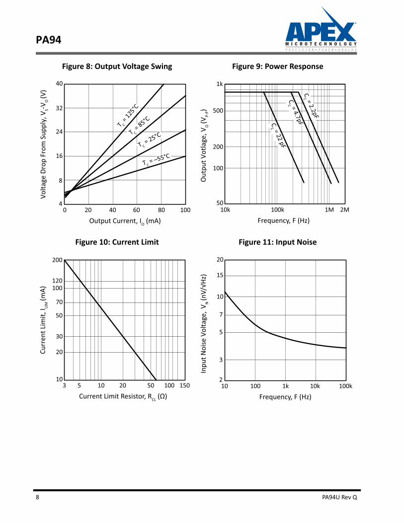
Figure 8: Output Voltage Swing Figure 9: Power Response
Figure 10: Current Limit Figure 11: Input Noise
40
32
24
16
8
40 20 40 60 10080
Output Current, IO (mA)
Volta
ge D
rop
From
Sup
ply,
VS-V
O (V
)
T C = 25°C
T C = –55°C
T C =
125°C
T C = 85°C
1k
500
200
100
5010k 100k 2M1M
Frequency, F (Hz)
Out
put V
otla
ge, V
O (V
P-P)
CC = 22 pF
CC = 4.7pF
CC = 2.2pF
200
120100
70
50
30
20
103 5 10 20 50 150100
Current Limit Resistor, RCL ( )
Curr
ent L
imit,
I LIM
(mA)
20
15
10
7
5
3
210 100 1k 100k10k
Frequency, F (Hz)
Inpu
t Noi
se V
olta
ge, V
N
8 PA94U Rev Q
PA94
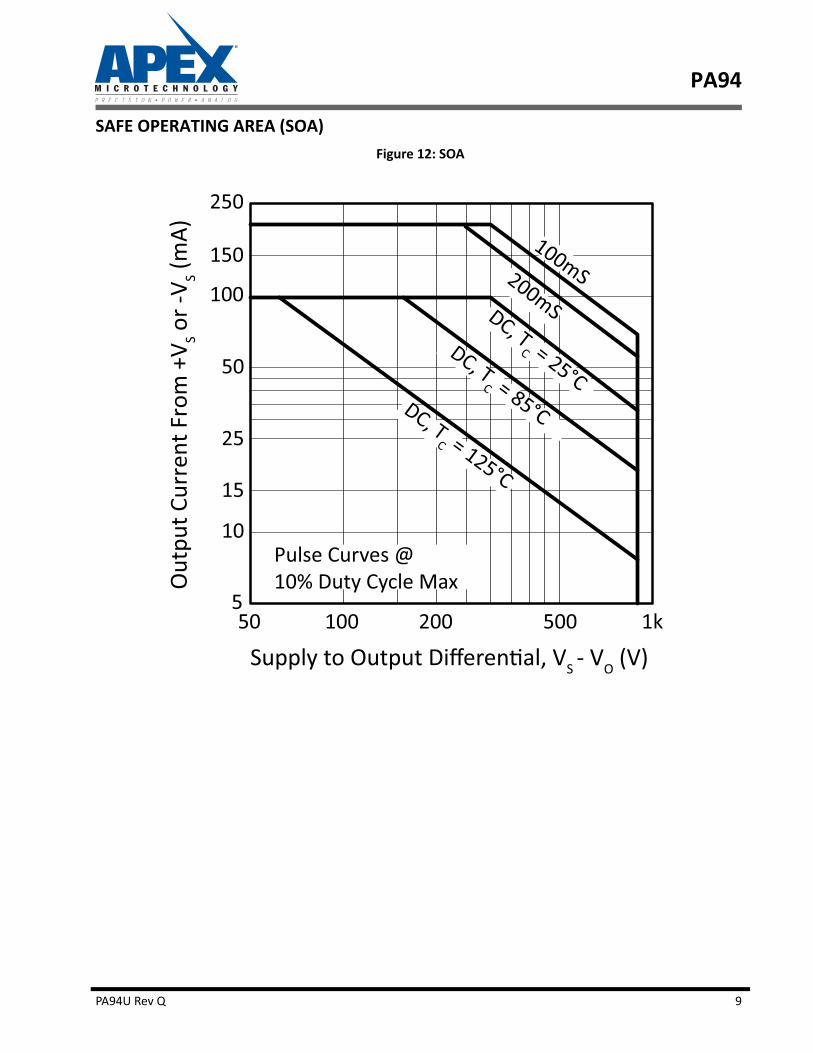
SAFE OPERATING AREA (SOA)
Figure 12: SOA
250
150
100
50
25
15
10
550 100 200 1k500
VS - VO (V)
V SV S
A)
C = 125°C
C = 85°C
C = 25°C
PA94U Rev Q 9

PA94
GENERAL
Please read Application Note 1 “General Operating Considerations” which covers stability, supplies, heatsinking, mounting, current limit, SOA interpretation, and specification interpretation. Visit www.apexana‐log.com for Apex Microtechnology’s complete Application Notes library, Technical Seminar Workbook, andEvaluation Kits.
TYPICAL APPLICATION
Piezo positioning may be applied to the focusing of segmented mirror systems. The composite mirrormay be composed of hundreds of elements, each requiring focusing under computer control. In such com‐plex systems the PA94 reduces the costs of power supplies and cooling with its advantages of low cost andlow quiescent power consumption while increasing circuit density with the SIP.
Figure 13: Typical Application
PHASE COMPENSATION
* CC rated for full supply voltage
INTERNAL POWER DISSIPATION AND HEATSINK SELECTION
With the unique combination of high voltage and speed of the PA94, traditional formulas for heatsinkselection will falsely lower the apparent power handling capability of this amplifier. To more accurately pre‐dict operating temperatures refer to Apex Microtechnology Applications Note 1, General Operating Consider‐ations, paragraph 7. Find total quiescent power (PDQ) by multiplying 0.024A by VSS (total supply voltage). Find
output stage quiescent power (PDQOUT) by multiplying 0.00012 by VSS.
Gain CC*
≥100 2.2pF
≥50 4.7pF
≥10 22pF
10 PA94U Rev Q

PA94
Calculate a heatsink rating which will maintain the case at 85°C or lower.
Where: TC = maximum case temperature allowed
TA = maximum ambient temperature encountered
Calculate a heatsink rating which will maintain output transistor junctions at 150°C or lower.
Where: TJ = maximum junction temperature allowed.
RØJC = AC or DC thermal resistance from the specification table.
Use the larger heatsink of these two calculations.
CURRENT LIMIT
For proper operation, the current limit resistor (RLIM) must be connected as shown in the typical connec‐
tion diagram. The minimum value is 3.5 ohm, however for optimum reliability the resistor value should be setas high as possible. The value is calculated as follows; with the maximum practical value of 30 ohms.
COMMON MODE INPUT RANGE
Operational amplifiers are usually designed to have a common mode input voltage range that approxi‐mates the power supply voltage range. However, to keep the cost as low as possible and still meet therequirements of most applications the common mode input voltage range of the PA94 is restricted. The inputpins must always be a least 30V from either supply voltage but never more than 450V. This means that thePA94 cannot be used in applications where the supply voltages are extremely unbalanced. For example, sup‐ply voltages of +800V and –100V would not be allowed in an application where the non‐inverting pin isgrounded because in normal operation both input pins would be at 0V and the difference voltage betweenthe positive supply and the input pins would be 800V. In this kind of application, however, supply voltages+450V and ‐100V does meet the input common mode voltage range requirements since the maximum differ‐ence voltage between the inputs pins and the supply voltage is 450V (the maximum allowed). The output hasno such restrictions on its voltage swing. The output can swing within 24V of either supply voltage regardlessof value so long as the total supply voltage does not exceed 900V.
INPUT PROTECTION
Although the PA94 can withstand differential input voltages up to ±20V, additional external protection isrecommended. In most applications 1N4148 or 1N914 signal diodes are sufficient (D1, D2 in Figure 14A). Inmore demanding applications where low leakage or low capacitance are of concern 2N4416 or 2N5457‐2N5459 JFETs connected as diodes will be required (Q1, Q2 in Figure 14B). In either case the input differentialvoltage will be clamped to ±0.7V. This is sufficient overdrive to produce maximum power bandwidth. Notethat this protection does not automatically protect the amplifier from excessive common mode input volt‐ages.
RSA
TC TA–
PD PDQ+-------------------------- 0.1
CW------–=
RSA
TJ TA– PD PDQOUT+ RJC–
PD PDQ+---------------------------------------------------------------------------------- 0.1
CW------–=
RLIM 0.7VILIM A -------------------=
PA94U Rev Q 11

PA94
Figure 14: Overvoltage Protection
POWER SUPPLY PROTECTION
Unidirectional zener diode transient suppressors are recommended as protection on the supply pins. Thezeners clamp transients to voltages within the power supply rating and also clamp power supply reversals toground. Whether the zeners are used or not, the system power supply should be evaluated for transient per‐formance including power‐on overshoot and power‐off polarity reversal as well as line regulation.Conditions which can cause open circuits or polarity reversals on either power supply rail should be avoidedor protected against. Reversals or opens on the negative supply rail is known to induce input stage failure.Unidirectional transzorbs prevent this, and it is desirable that they be both electrically and physically as closeto the amplifier as possible.
STABILITY
The PA94 is stable at gains of 100 or more with a NPO (COG) compensation capacitor of 2.2pF. The com‐pensation capacitor, Cc, in the external connections diagram must be rated at 1000V working voltage andmounted closely to pins 4 and 6 to prevent spurious oscillation. A compensation capacitor less than 2.2pF isnot recommended.
EXTERNAL COMPONENTS
The compensation capacitor Cc must be rated for the total supply voltage. An NPO (COG) capacitor rateda 1kV is recommended.
Of equal importance are the voltage rating and voltage coefficient of the gain setting feedback resistor.Typical voltage ratings of low wattage resistors are 150 to 250V. Up to 500 V can appear across the feedbackresistor. High voltage rated resistors can be obtained. However a 1 MΩ feedback resistor composed of five200k resistors in series will produce the proper voltage rating.
CAUTIONS
The operating voltages of the PA94 are potentially lethal. During circuit design develop a functioning cir‐cuit at the lowest possible voltages. Clip test leads should be used for “hands off” measurements while trou‐bleshooting.
12 PA94U Rev Q
PA94
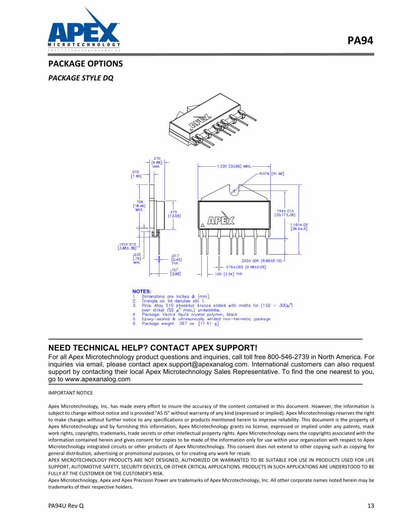
PACKAGE OPTIONS
PACKAGE STYLE DQ
PA94U Rev Q 13
NEED TECHNICAL HELP? CONTACT APEX SUPPORT! For all Apex Microtechnology product questions and inquiries, call toll free 800-546-2739 in North America. Forinquiries via email, please contact [email protected]. International customers can also requestsupport by contacting their local Apex Microtechnology Sales Representative. To find the one nearest to you,go to www.apexanalog.com
IMPORTANT NOTICE
Apex Microtechnology, Inc. has made every effort to insure the accuracy of the content contained in this document. However, the information is
subject to change without notice and is provided "AS IS" without warranty of any kind (expressed or implied). Apex Microtechnology reserves the right
to make changes without further notice to any specifications or products mentioned herein to improve reliability. This document is the property ofApex Microtechnology and by furnishing this information, Apex Microtechnology grants no license, expressed or implied under any patents, mask
work rights, copyrights, trademarks, trade secrets or other intellectual property rights. Apex Microtechnology owns the copyrights associated with the
information contained herein and gives consent for copies to be made of the information only for use within your organization with respect to ApexMicrotechnology integrated circuits or other products of Apex Microtechnology. This consent does not extend to other copying such as copying for
general distribution, advertising or promotional purposes, or for creating any work for resale.
APEX MICROTECHNOLOGY PRODUCTS ARE NOT DESIGNED, AUTHORIZED OR WARRANTED TO BE SUITABLE FOR USE IN PRODUCTS USED FOR LIFESUPPORT, AUTOMOTIVE SAFETY, SECURITY DEVICES, OR OTHER CRITICAL APPLICATIONS. PRODUCTS IN SUCH APPLICATIONS ARE UNDERSTOOD TO BE
FULLY AT THE CUSTOMER OR THE CUSTOMER’S RISK.
Apex Microtechnology, Apex and Apex Precision Power are trademarks of Apex Microtechnology, Inc. All other corporate names noted herein may betrademarks of their respective holders.


![UK BS 7671 16 VDE 0100 EN-60601/60335/60950/61010 VDE …download.flukecal.com/pub/literature/Fluke... · 2 [1] 50 kΩ 60 kΩ 100 kΩ / 20 V 500,000 8 10 kΩ 10 GΩ 4.5 CE Low Voltage](https://static.fdocuments.net/doc/165x107/5e7807e35be0b42eba4126eb/uk-bs-7671-16-vde-0100-en-60601603356095061010-vde-2-1-50-k-60-k-100-k.jpg)