P89C660/P89C662/P89C664/P89C668 80C51 8-bit Flash ... · The added features of the...
89
Philips Semiconductors P89C660/P89C662/P89C664/P89C668 80C51 8-bit Flash microcontroller family 16KB/32KB/64KB ISP/IAP FLASH with 512B/1KB/2KB/8KB RAM Product data Replaces P89C660/P89C662/P89C664 of 2001 Jul 19 and P89C668 of 2001 Jul 27 2002 Oct 28 INTEGRATED CIRCUITS
Transcript of P89C660/P89C662/P89C664/P89C668 80C51 8-bit Flash ... · The added features of the...

P89C660/P89C662/P89C664/P89C66880C51 8-bit Flash microcontroller family16KB/32KB/64KB ISP/IAP FLASH with 512B/1KB/2KB/8KB RAM
Product dataReplaces P89C660/P89C662/P89C664 of 2001 Jul 19and P89C668 of 2001 Jul 27
2002 Oct 28
INTEGRATED CIRCUITS

Philips Semiconductors Product data
P89C660/P89C662/P89C664/P89C668
80C51 8-bit Flash microcontroller family16KB/32KB/64KB ISP/IAP Flash with 512B/1KB/2KB/8KB RAM
22002 Oct 28 853-2392 29118
DESCRIPTIONThe P89C660/662/664/668 device contains a non-volatile16KB/32KB/64KB Flash program memory that is both parallelprogrammable and serial In-System and In-ApplicationProgrammable. In-System Programming (ISP) allows the user todownload new code while the microcontroller sits in the application.In-Application Programming (IAP) means that the microcontrollerfetches new program code and reprograms itself while in thesystem. This allows for remote programming over a modem link.A default serial loader (boot loader) program in ROM allows serialIn-System Programming of the Flash memory via the UART withoutthe need for a loader in the Flash code. For In-ApplicationProgramming, the user program erases and reprograms the Flashmemory by use of standard routines contained in ROM.
This device executes one instruction in 6 clock cycles, henceproviding twice the speed of a conventional 80C51. An OTPconfiguration bit gives the user the option to select conventional12-clock timing.
This device is a Single-Chip 8-Bit Microcontroller manufactured inadvanced CMOS process and is a derivative of the 80C51microcontroller family. The instruction set is 100% executing andtiming compatible with the 80C51 instruction set.
The device also has four 8-bit I/O ports, three 16-bit timer/eventcounters, a multi-source, four-priority-level, nested interruptstructure, an enhanced UART and on-chip oscillator and timingcircuits.
The added features of the P89C660/662/664/668 makes it apowerful microcontroller for applications that require pulse widthmodulation, high-speed I/O and up/down counting capabilities suchas motor control.
FEATURES• 80C51 Central Processing Unit
• On-chip Flash program memory with In-System Programming(ISP) and In-Application Programming (IAP) capability
• Boot ROM contains low level Flash programming routines fordownloading via the UART
• Can be programmed by the end-user application (IAP)
• Parallel programming with 87C51 compatible hardware interfaceto programmer
• Six clocks per machine cycle operation (standard)
• 12 clocks per machine cycle operation (optional)
• Speed up to 20 MHz with 6 clock cycles per machine cycle(40 MHz equivalent performance); up to 33 MHz with 12 clocksper machine cycle
• Fully static operation
• RAM externally expandable to 64 kbytes
• Four interrupt priority levels
• Eight interrupt sources
• Four 8-bit I/O ports
• Full-duplex enhanced UART
– Framing error detection
– Automatic address recognition
• Power control modes
– Clock can be stopped and resumed
– Idle mode
– Power-Down mode
• Programmable clock out
• Second DPTR register
• Asynchronous port reset
• Low EMI (inhibit ALE)
• I2C serial interface
• Programmable Counter Array (PCA)
– PWM
– Capture/compare
• Well-suited for IPMI applications

Philips Semiconductors Product data
P89C660/P89C662/P89C664/P89C668
80C51 8-bit Flash microcontroller family16KB/32KB/64KB ISP/IAP Flash with 512B/1KB/2KB/8KB RAM
2002 Oct 28 3
SELECTION TABLE
Type Memory Timers Serial Inter-faces
RA
M
RO
M
OT
P
Fla
sh
# of
Tim
ers
PW
M
PC
A
WD
UA
RT
I2C
CA
N
SP
I
AD
C b
its/c
h.
I/O P
ins
Inte
rrup
ts
(Ext
erna
l)
Pro
gram
S
ecur
ity
Def
ault
Clo
ckR
ate
Opt
iona
lC
lock
Rat
e
Res
et a
ctiv
elo
w/h
igh?
Max. Freq.at 6-clk/ 12-clk(MHz)
Freq.Rangeat 3V(MHz)
Freq.Rangeat 5V(MHz)
P89C668 8K – – 64K 4 √ √ √ √ √ – – – 32 8(2)/4 √ 6-clk 12-clk H 20/33 – 0-20/33
P89C664 2K – – 64K 4 √ √ √ √ √ – – – 32 8(2)/4 √ 6-clk 12-clk H 20/33 – 0-20/33
P89C662 1K – – 32K 4 √ √ √ √ √ – – – 32 8(2)/4 √ 6-clk 12-clk H 20/33 – 0-20/33
P89C660 512B – – 16K 4 √ √ √ √ √ – – – 32 8(2)/4 √ 6-clk 12-clk H 20/33 – 0-20/33
ORDERING INFORMATIONMEMORY
TEMPERATURE RANGE (°C) VOLTAGEFREQUENCY (MHz)
DEVICE FLASH RAMTEMPERATURE RANGE (°C)
AND PACKAGEVOLTAGERANGE 6 CLOCK MODE 12 CLOCK
MODEDWG #
P89C660HBA 16 KB 512 B 0 to +70, PLCC 4.5–5.5 V 0 to 20 MHz 0 to 33 MHz SOT187-2
P89C660HFA 16 KB 512 B –40 to +85, PLCC 4.75–5.25 V 0 to 20 MHz 0 to 33 MHz SOT187-2
P89C660HBBD 16 KB 512 B 0 to +70, LQFP 4.5–5.5 V 0 to 20 MHz 0 to 33 MHz SOT389-1
P89C662HBA 32 KB 1 KB 0 to +70, PLCC 4.5–5.5 V 0 to 20 MHz 0 to 33 MHz SOT187-2
P89C662HFA 32 KB 1 KB –40 to +85, PLCC 4.75–5.25 V 0 to 20 MHz 0 to 33 MHz SOT187-2
P89C662HBBD 32 KB 1 KB 0 to +70, LQFP 4.5–5.5 V 0 to 20 MHz 0 to 33 MHz SOT389-1
P89C662HFBD 32 KB 1 KB –40 to +85, LQFP 4.75–5.25 V 0 to 20 MHz 0 to 33 MHz SOT389-1
P89C664HBA 64 KB 2 KB 0 to +70, PLCC 4.5–5.5 V 0 to 20 MHz 0 to 33 MHz SOT187-2
P89C664HFA 64 KB 2 KB –40 to +85, PLCC 4.75–5.25 V 0 to 20 MHz 0 to 33 MHz SOT187-2
P89C664HBBD 64 KB 2 KB 0 to +70, LQFP 4.5–5.5 V 0 to 20 MHz 0 to 33 MHz SOT389-1
P89C664HFBD 64 KB 2 KB –40 to +85, LQFP 4.75–5.25 V 0 to 20 MHz 0 to 33 MHz SOT389-1
P89C668HBA 64 KB 8 KB 0 to +70, PLCC 4.5–5.5 V 0 to 20 MHz 0 to 33 MHz SOT187-2
P89C668HFA 64 KB 8 KB –40 to +85, PLCC 4.5–5.5 V 0 to 20 MHz 0 to 33 MHz SOT187-2
P89C668HBBD 64 KB 8 KB 0 to +70, LQFP 4.5–5.5 V 0 to 20 MHz 0 to 33 MHz SOT389-1

Philips Semiconductors Product data
P89C660/P89C662/P89C664/P89C668
80C51 8-bit Flash microcontroller family16KB/32KB/64KB ISP/IAP Flash with 512B/1KB/2KB/8KB RAM
2002 Oct 28 4
BLOCK DIAGRAM 1
su01713
ACCELERATED 80C51 CPU6-CLK MODE (DEFAULT)
12-CLK MODE (OPTIONAL)
16K / 32K / 64 KBYTE
CODE FLASH
0.5K / 1K / 2K /8 KBYTE DATA RAM
PORT 3CONFIGURABLE I/Os
PORT 2CONFIGURABLE I/Os
PORT 1CONFIGURABLE I/Os
PORT 0CONFIGURABLE I/Os
OSCILLATORCRYSTAL ORRESONATOR
FULL-DUPLEXENHANCED UART
TIMER 0TIMER 1
TIMER 2
PROGRAMMABLECOUNTER ARRAY
(PCA)
WATCHDOG TIMER
I2CINTERFACE

Philips Semiconductors Product data
P89C660/P89C662/P89C664/P89C668
80C51 8-bit Flash microcontroller family16KB/32KB/64KB ISP/IAP Flash with 512B/1KB/2KB/8KB RAM
2002 Oct 28 5
BLOCK DIAGRAM (CPU-ORIENTED)
su01089
PSEN
EA/VPP
ALE
RST
XTAL1 XTAL2
VCC
VSS
PORT 0DRIVERS
PORT 2DRIVERS
RAM ADDRREGISTER RAM PORT 0
LATCHPORT 2LATCH
FLASH
REGISTERB
ACC STACKPOINTER
TMP2 TMP1
ALU
TIMINGAND
CONTROL
INS
TR
UC
TIO
N
RE
GIS
TE
R
PD
OSCILLATOR
PSW
PORT 1LATCH
PORT 3LATCH
PORT 1 DRIVERS
PORT 3DRIVERS
PROGRAMADDRESSREGISTER
BUFFER
PCINCRE-
MENTER
PROGRAMCOUNTER
DPTR’SMULTIPLE
P1.0–P1.7 P3.0–P3.7
P0.0–P0.7 P2.0–P2.7
SFRs
TIMERS
P.C.A.
8
8 16
I2C
SCL
SDA
Philips Semiconductors Product data
P89C660/P89C662/P89C664/P89C668
80C51 8-bit Flash microcontroller family16KB/32KB/64KB ISP/IAP Flash with 512B/1KB/2KB/8KB RAM
2002 Oct 28 6
LOGIC SYMBOL
PO
RT
0P
OR
T 1
PO
RT
2
PO
RT
3
ADDRESS AND
DATA BUS
ADDRESS BUS
T2T2EX
RxD
TxDINT0
INT1T0T1
WRRD
SE
CO
ND
AR
Y F
UN
CT
ION
S
RSTEA/VPP
PSEN
ALE/PROG
VSSVCC
XTAL1
XTAL2
SU01090
SCLSDA
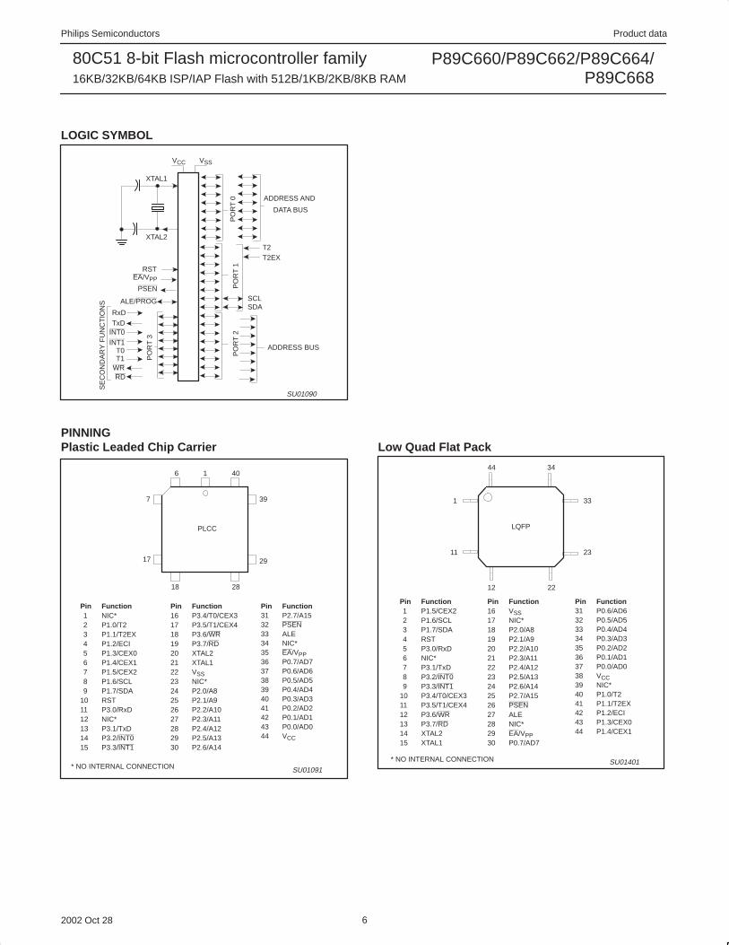
PINNINGPlastic Leaded Chip Carrier
SU01091
PLCC
6 1 40
7
17
39
29
18 28
Pin Function1 NIC*2 P1.0/T23 P1.1/T2EX4 P1.2/ECI5 P1.3/CEX06 P1.4/CEX17 P1.5/CEX28 P1.6/SCL9 P1.7/SDA
10 RST11 P3.0/RxD12 NIC*13 P3.1/TxD14 P3.2/INT015 P3.3/INT1
Pin Function16 P3.4/T0/CEX317 P3.5/T1/CEX418 P3.6/WR19 P3.7/RD20 XTAL221 XTAL122 VSS23 NIC*24 P2.0/A825 P2.1/A926 P2.2/A1027 P2.3/A1128 P2.4/A1229 P2.5/A1330 P2.6/A14
Pin Function31 P2.7/A1532 PSEN33 ALE34 NIC*35 EA/VPP36 P0.7/AD737 P0.6/AD638 P0.5/AD539 P0.4/AD440 P0.3/AD341 P0.2/AD242 P0.1/AD143 P0.0/AD044 VCC
* NO INTERNAL CONNECTION
Low Quad Flat Pack
SU01401
LQFP
44 34
1
11
33
23
12 22
Pin Function1 P1.5/CEX22 P1.6/SCL3 P1.7/SDA4 RST5 P3.0/RxD6 NIC*7 P3.1/TxD8 P3.2/INT09 P3.3/INT1
10 P3.4/T0/CEX311 P3.5/T1/CEX412 P3.6/WR13 P3.7/RD14 XTAL215 XTAL1
Pin Function16 VSS17 NIC*18 P2.0/A819 P2.1/A920 P2.2/A1021 P2.3/A1122 P2.4/A1223 P2.5/A1324 P2.6/A1425 P2.7/A1526 PSEN27 ALE28 NIC*29 EA/VPP30 P0.7/AD7
Pin Function31 P0.6/AD632 P0.5/AD533 P0.4/AD434 P0.3/AD335 P0.2/AD236 P0.1/AD137 P0.0/AD038 VCC39 NIC*40 P1.0/T241 P1.1/T2EX42 P1.2/ECI43 P1.3/CEX044 P1.4/CEX1
* NO INTERNAL CONNECTION

Philips Semiconductors Product data
P89C660/P89C662/P89C664/P89C668
80C51 8-bit Flash microcontroller family16KB/32KB/64KB ISP/IAP Flash with 512B/1KB/2KB/8KB RAM
2002 Oct 28 7
PIN DESCRIPTIONS
MNEMONICPIN NUMBER
TYPE NAME AND FUNCTIONMNEMONICPLCC LQFP
TYPE NAME AND FUNCTION
VSS 22 16 I Ground: 0 V reference.
VCC 44 38 I Power Supply: This is the power supply voltage for normal, idle, and power-down operation.
P0.0–0.7 43–36 37–30 I/O Port 0: Port 0 is an open-drain, bidirectional I/O port. Port 0 pins that have 1s written to themfloat and can be used as high-impedance inputs. Port 0 is also the multiplexed low-orderaddress and data bus during accesses to external program and data memory. In thisapplication, it uses strong internal pull-ups when emitting 1s.
P1.0–P1.7 2–9 40–44,1–3
I/O Port 1: Port 1 is an 8-bit bidirectional I/O port with internal pull-ups on all pins except P1.6 andP1.7 which are open drain. Port 1 pins that have 1s written to them are pulled high by theinternal pull-ups and can be used as inputs. As inputs, port 1 pins that are externally pulled lowwill source current because of the internal pull-ups. (See DC Electrical Characteristics: IIL).
Alternate functions for P89C660/662/664/668 Port 1 include:
2 40 I/O T2 (P1.0): Timer/Counter 2 external count input/Clockout (see Programmable Clock-Out)
3 41 I T2EX (P1.1): Timer/Counter 2 Reload/Capture/Direction Control
4 42 I ECI (P1.2): External Clock Input to the PCA
5 43 I/O CEX0 (P1.3): Capture/Compare External I/O for PCA module 0
6 44 I/O CEX1 (P1.4): Capture/Compare External I/O for PCA module 1
7 1 I/O CEX2 (P1.5): Capture/Compare External I/O for PCA module 2
8 2 I/O SCL (P1.6): I2C bus clock line (open drain)
9 3 I/O SDA (P1.7): I2C bus data line (open drain)
P2.0–P2.7 24–31 18–25 I/O Port 2: Port 2 is an 8-bit bidirectional I/O port with internal pull-ups. Port 2 pins that have 1swritten to them are pulled high by the internal pull-ups and can be used as inputs. As inputs,port 2 pins that are externally being pulled low will source current because of the internalpull-ups. (See DC Electrical Characteristics: IIL). Port 2 emits the high-order address byteduring fetches from external program memory and during accesses to external data memorythat use 16-bit addresses (MOVX @DPTR). In this application, it uses strong internal pull-upswhen emitting 1s. During accesses to external data memory that use 8-bit addresses (MOV@Ri), port 2 emits the contents of the P2 special function register.
P3.0–P3.7 11,13–19
5, 7–13 I/O Port 3: Port 3 is an 8-bit bidirectional I/O port with internal pull-ups. Port 3 pins that have 1swritten to them are pulled high by the internal pull-ups and can be used as inputs. As inputs,port 3 pins that are externally being pulled low will source current because of the pull-ups. (SeeDC Electrical Characteristics: IIL). Port 3 also serves the special features of theP89C660/662/664/668, as listed below:
11 5 I RxD (P3.0): Serial input port
13 7 O TxD (P3.1): Serial output port
14 8 I INT0 (P3.2): External interrupt
15 9 I INT1 (P3.3): External interrupt
16 10 I CEX3/T0 (P3.4): Timer 0 external input; Capture/Compare External I/O for PCA module 3
17 11 I CEX4/T1 (P3.5): Timer 1 external input; Capture/Compare External I/O for PCA module 4
18 12 O WR (P3.6): External data memory write strobe
19 13 O RD (P3.7): External data memory read strobe
RST 10 4 I Reset: A high on this pin for two machine cycles while the oscillator is running, resets thedevice. An internal resistor to VSS permits a power-on reset using only an external capacitor toVCC.
ALE 33 27 O Address Latch Enable: Output pulse for latching the low byte of the address during an accessto external memory. In normal operation, ALE is emitted twice every machine cycle, and can beused for external timing or clocking. Note that one ALE pulse is skipped during each access toexternal data memory. ALE can be disabled by setting SFR auxiliary.0. With this bit set, ALEwill be active only during a MOVX instruction.
PSEN 32 26 O Program Store Enable: The read strobe to external program memory. When executing codefrom the external program memory, PSEN is activated twice each machine cycle, except thattwo PSEN activations are skipped during each access to external data memory. PSEN is notactivated during fetches from internal program memory.

Philips Semiconductors Product data
P89C660/P89C662/P89C664/P89C668
80C51 8-bit Flash microcontroller family16KB/32KB/64KB ISP/IAP Flash with 512B/1KB/2KB/8KB RAM
2002 Oct 28 8
MNEMONIC NAME AND FUNCTIONTYPEPIN NUMBER
MNEMONIC NAME AND FUNCTIONTYPELQFPPLCC
EA/VPP 35 29 I External Access Enable/Programming Supply Voltage: EA must be externally held low toenable the device to fetch code from external program memory locations. If EA is held high, thedevice executes from internal program memory. The value on the EA pin is latched when RSTis released and any subsequent changes have no effect. This pin also receives theprogramming supply voltage (VPP) during Flash programming.
XTAL1 21 15 I Crystal 1: Input to the inverting oscillator amplifier and input to the internal clock generatorcircuits.
XTAL2 20 14 O Crystal 2: Output from the inverting oscillator amplifier.
NOTE:To avoid “latch-up” effect at power-on, the voltage on any pin (other than VPP) must not be higher than VCC + 0.5 V or less than VSS – 0.5 V.

Philips Semiconductors Product data
P89C660/P89C662/P89C664/P89C668
80C51 8-bit Flash microcontroller family16KB/32KB/64KB ISP/IAP Flash with 512B/1KB/2KB/8KB RAM
2002 Oct 28 9
Table 1. Special Function Registers
SYMBOL DESCRIPTION DIRECTADDRESS
BIT ADDRESS, SYMBOL, OR ALTERNATIVE PORT FUNCTION MSB LSB
RESETVALUE
ACC* Accumulator E0H E7 E6 E5 E4 E3 E2 E1 E0 00H
AUXR# Auxiliary 8EH – – – – – – EXTRAM AO xxxxxx10B
AUXR1# Auxiliary 1 A2H – – ENBOOT – GF2 0 – DPS xxxxx0x0B
B* B register F0H F7 F6 F5 F4 F3 F2 F1 F0 00H
CCAP0H# Module 0 Capture High FAH xxxxxxxxBCCAP1H# Module 1 Capture High FBH xxxxxxxxBCCAP2H# Module 2 Capture High FCH xxxxxxxxBCCAP3H# Module 3 Capture High FDH xxxxxxxxBCCAP4H# Module 4 Capture High FEH xxxxxxxxBCCAP0L# Module 0 Capture Low EAH xxxxxxxxBCCAP1L# Module 1 Capture Low EBH xxxxxxxxBCCAP2L# Module 2 Capture Low ECH xxxxxxxxBCCAP3L# Module 3 Capture Low EDH xxxxxxxxBCCAP4L# Module 4 Capture Low EEH xxxxxxxxB
CCAPM0# Module 0 Mode C2H – ECOM CAPP CAPN MAT TOG PWM ECCF x0000000B
CCAPM1# Module 1 Mode C3H – ECOM CAPP CAPN MAT TOG PWM ECCF x0000000B
CCAPM2# Module 2 Mode C4H – ECOM CAPP CAPN MAT TOG PWM ECCF x0000000B
CCAPM3# Module 3 Mode C5H – ECOM CAPP CAPN MAT TOG PWM ECCF x0000000B
CCAPM4# Module 4 Mode C6H – ECOM CAPP CAPN MAT TOG PWM ECCF x0000000B
C7 C6 C5 C4 C3 C2 C1 C0
CCON*# PCA Counter Control C0H CF CR – CCF4 CCF3 CCF2 CCF1 CCF0 00x00000BCH# PCA Counter High F9H 00HCL# PCA Counter Low E9H 00H
CMOD# PCA Counter Mode C1H CIDL WDTE – – – CPS1 CPS0 ECF 00xxx000B
DPTR: Data Pointer (2 bytes) DPH Data Pointer High 83H 00H DPL Data Pointer Low 82H 00H
AF AE AD AC AB AA A9 A8
IEN0* Interrupt Enable 0 A8H EA EC ES1 ES0 ET1 EX1 ET0 EX0 00H
IEN1* Interrupt Enable 1 E8 – – – – – – – ET2 xxxxxxx0B
BF BE BD BC BB BA B9 B8
IP* Interrupt Priority B8H PT2 PPC PS1 PS0 PT1 PX1 PT0 PX0 x0000000B
IPH# Interrupt Priority High B7H PT2H PPCH PS1H PS0H PT1H PX1H PT0H PX0H x0000000B
87 86 85 84 83 82 81 80
P0* Port 0 80H AD7 AD6 AD5 AD4 AD3 AD2 AD1 AD0 FFH
97 96 95 94 93 92 91 90
P1* Port 1 90H SDA SCL CEX2 CEX1 CEX0 ECI T2EX T2 FFH
A7 A6 A5 A4 A3 A2 A1 A0
P2* Port 2 A0H AD15 AD14 AD13 AD12 AD11 AD10 AD9 AD8 FFH
B7 B6 B5 B4 B3 B2 B1 B0
P3* Port 3 B0H RD WR T1/CEX4
T0/CEX3
INT1 INT0 TxD RxD FFH
PCON#1 Power Control 87H SMOD1 SMOD0 – POF GF1 GF0 PD IDL 00xxx000B
* SFRs are bit addressable.# SFRs are modified from or added to the 80C51 SFRs.– Reserved bits.1. Reset value depends on reset source.

Philips Semiconductors Product data
P89C660/P89C662/P89C664/P89C668
80C51 8-bit Flash microcontroller family16KB/32KB/64KB ISP/IAP Flash with 512B/1KB/2KB/8KB RAM
2002 Oct 28 10
Table 1 Special Function Registers (Continued)
SYMBOL DESCRIPTION DIRECTADDRESS
BIT ADDRESS, SYMBOL, OR ALTERNATIVE PORT FUNCTION MSB LSB
RESETVALUE
D7 D6 D5 D4 D3 D2 D1 D0
PSW* Program Status Word D0H CY AC F0 RS1 RS0 OV F1 P 00000000B
RCAP2H# Timer 2 Capture High CBH 00HRCAP2L# Timer 2 Capture Low CAH 00H
SADDR# Slave Address A9H 00HSADEN# Slave Address Mask B9H 00H
S0BUF Serial Data Buffer 99H xxxxxxxxB
9F 9E 9D 9C 9B 9A 99 98
S0CON* Serial Control 98H SM0/FE SM1 SM2 REN TB8 RB8 TI RI 00H
SP Stack Pointer 81H 07H
S1DAT# Serial 1 Data DAH 00H
S1ADR# Serial 1 Address DBH SLAVE ADDRESS GC 00H
S1STA# Serial 1 Status D9H SC4 SC3 SC2 SC1 SC0 0 0 0 F8H
DF DE DD DC DB DA D9 D8
S1CON*# Serial 1 Control D8H CR2 ENS1 STA STO SI AA CR1 CR0 00000000B
8F 8E 8D 8C 8B 8A 89 88
TCON* Timer Control 88H TF1 TR1 TF0 TR0 IE1 IT1 IE0 IT0 00H
CF CE CD CC CB CA C9 C8
T2CON* Timer 2 Control C8H TF2 EXF2 RCLK TCLK EXEN2 TR2 C/T2 CP/RL2 00H
T2MOD# Timer 2 Mode Control C9H – – – – – – T2OE DCEN xxxxxx00B
TH0 Timer High 0 8CH 00HTH1 Timer High 1 8DH 00HTH2# Timer High 2 CDH 00HTL0 Timer Low 0 8AH 00HTL1 Timer Low 1 8BH 00HTL2# Timer Low 2 CCH 00H
TMOD Timer Mode 89H GATE C/T M1 M0 GATE C/T M1 M0 00H
WDTRST Watchdog Timer Reset A6H
* SFRs are bit addressable.# SFRs are modified from or added to the 80C51 SFRs.– Reserved bits.
OSCILLATOR CHARACTERISTICSXTAL1 and XTAL2 are the input and output, respectively, of aninverting amplifier. The pins can be configured for use as anon-chip oscillator.
To drive the device from an external clock source, XTAL1 should bedriven while XTAL2 is left unconnected. Minimum and maximumhigh and low times specified in the data sheet must be observed.
This device is configured at the factory to operate using 6 clockperiods per machine cycle, referred to in this datasheet as “6 clockmode”. (This yields performance equivalent to twice that of standard80C51 family devices). It may be optionally configured oncommercially-available EPROM programming equipment to operateat 12 clock periods per machine cycle, referred to in this datasheetas “12 clock mode”. Once 12 clock mode has been configured, itcannot be changed back to 6 clock mode.
RESETA reset is accomplished by holding the RST pin high for at least twomachine cycles (12 oscillator periods in 6 clock mode, or 24oscillator periods in 12 clock mode), while the oscillator is running.To insure a good power-on reset, the RST pin must be high longenough to allow the oscillator time to start up (normally a fewmilliseconds) plus two machine cycles. At power-on, the voltage onVCC and RST must come up at the same time for a proper start-up.Ports 1, 2, and 3 will asynchronously be driven to their resetcondition when a voltage above VIH1 (min.) is applied to RST.
The value on the EA pin is latched when RST is deasserted and hasno further effect.

Philips Semiconductors Product data
P89C660/P89C662/P89C664/P89C668
80C51 8-bit Flash microcontroller family16KB/32KB/64KB ISP/IAP Flash with 512B/1KB/2KB/8KB RAM
2002 Oct 28 11
LOW POWER MODES
Stop Clock ModeThe static design enables the clock speed to be reduced down to0 MHz (stopped). When the oscillator is stopped, the RAM andSpecial Function Registers retain their values. This mode allowsstep-by-step utilization and reduces system power consumption bylowering the clock frequency down to any value. For lowest powerconsumption the Power-Down mode is suggested.
Idle ModeIn the idle mode (see Table 2), the CPU puts itself to sleep while allof the on-chip peripherals stay active. The instruction to invoke theidle mode is the last instruction executed in the normal operatingmode before the idle mode is activated. The CPU contents, theon-chip RAM, and all of the special function registers remain intactduring this mode. The idle mode can be terminated either by anyenabled interrupt (at which time the process is picked up at theinterrupt service routine and continued), or by a hardware resetwhich starts the processor in the same manner as a power-on reset.
Power-Down ModeTo save even more power, a Power-Down mode (see Table 2) canbe invoked by software. In this mode, the oscillator is stopped andthe instruction that invoked Power-Down is the last instructionexecuted. The on-chip RAM and Special Function Registers retaintheir values down to 2.0 V and care must be taken to return VCC tothe minimum specified operating voltages before the Power-Downmode is terminated.
Either a hardware reset or external interrupt can be used to exit fromPower-Down. Reset redefines all the SFRs but does not change theon-chip RAM. An external interrupt allows both the SFRs and theon-chip RAM to retain their values.
To properly terminate Power-Down the reset or external interruptshould not be executed before VCC is restored to its normaloperating level and must be held active long enough for theoscillator to restart and stabilize (normally less than 10ms).
With an external interrupt, INT0 and INT1 must be enabled andconfigured as level-sensitive. Holding the pin low restarts theoscillator, but bringing the pin back high completes the exit. Once theinterrupt is serviced, the next instruction to be executed after RETIwill be the one following the instruction that put the device intoPower-Down.
POWER-ON FLAGThe Power-On Flag (POF) is set by on-chip circuitry when the VCClevel on the P89C660/662/664/668 rises from 0 to 5 V. The POF bitcan be set or cleared by software allowing a user to determine ifthe reset is the result of a power-on or a warm start afterPower-Down. The VCC level must remain above 3 V for the POF toremain unaffected by the VCC level.
Design ConsiderationWhen the idle mode is terminated by a hardware reset, the devicenormally resumes program execution, from where it left off, up totwo machine cycles before the internal reset algorithm takes control.On-chip hardware inhibits access to internal RAM in this event,however, access to the port pins is not inhibited. To eliminate thepossibility of an unexpected write when the idle mode is terminatedby reset, the instruction following the one that invokes the idle modeshould not be one that writes to a port pin or to external memory.
ONCE ModeThe ONCE (“On-Circuit Emulation”) mode facilitates testing anddebugging of systems without the device having to be removed fromthe circuit. The ONCE mode is invoked by:
1. Pulling ALE low while the device is in reset and PSEN is high;
2. Holding ALE low as RST is deactivated.
While the device is in ONCE mode, the Port 0 pins go into a floatstate, and the other port pins and ALE and PSEN are weakly pulledhigh. The oscillator circuit remains active. While the device is in thismode, an emulator or test CPU can be used to drive the circuit.Normal operation is restored when a normal reset is applied.
Programmable Clock-OutA 50% duty cycle clock can be programmed to come out on P1.0.This pin, besides being a regular I/O pin, has two alternatefunctions. It can be programmed:
1. to input the external clock for Timer/Counter 2, or
2. to output a 50% duty cycle clock ranging from 122 Hz to 8 MHzat a 16 MHz operating frequency (61 Hz to 4 MHz in 12 clockmode).
To configure the Timer/Counter 2 as a clock generator, bit C/T2 (inT2CON) must be cleared and bit T20E in T2MOD must be set. BitTR2 (T2CON.2) also must be set to start the timer.
The Clock-Out frequency depends on the oscillator frequency andthe reload value of Timer 2 capture registers (RCAP2H, RCAP2L)as shown in this equation:
Oscillator Frequencyn (65536 RCAP2H, RCAP2L)
n = 2 in 6 clock mode4 in 12 clock mode
Where (RCAP2H,RCAP2L) = the content of RCAP2H and RCAP2Ltaken as a 16-bit unsigned integer.
In the Clock-Out mode Timer 2 roll-overs will not generate aninterrupt. This is similar to when it is used as a baud-rate generator.It is possible to use Timer 2 as a baud-rate generator and a clockgenerator simultaneously. Note, however, that the baud-rate and theClock-Out frequency will be the same.
Table 2. External Pin Status During Idle and Power-Down modeMODE PROGRAM MEMORY ALE PSEN PORT 0 PORT 1 PORT 2 PORT 3
Idle Internal 1 1 Data Data Data Data
Idle External 1 1 Float Data Address Data
Power-Down Internal 0 0 Data Data Data Data
Power-Down External 0 0 Float Data Data Data
Philips Semiconductors Product data
P89C660/P89C662/P89C664/P89C668
80C51 8-bit Flash microcontroller family16KB/32KB/64KB ISP/IAP Flash with 512B/1KB/2KB/8KB RAM
2002 Oct 28 12
I2C SERIAL COMMUNICATION — SIO1The I2C serial port is identical to the I2C serial port on the 8XC554,8XC654, and 8XC652 devices.
Note that the P89C660/662/664/668 I2C pins are alternatefunctions to port pins P1.6 and P1.7. Because of this, P1.6 andP1.7 on these parts do not have a pull-up structure as found on the80C51. Therefore P1.6 and P1.7 have open drain outputs on theP89C660/662/664/668.
The I2C bus uses two wires (SDA and SCL) to transfer informationbetween devices connected to the bus. The main features of the busare:– Bidirectional data transfer between masters and slaves
– Multimaster bus (no central master)
– Arbitration between simultaneously transmitting masters withoutcorruption of serial data on the bus
– Serial clock synchronization allows devices with different bit ratesto communicate via one serial bus
– Serial clock synchronization can be used as a handshakemechanism to suspend and resume serial transfer
– The I2C bus may be used for test and diagnostic purposes
The output latches of P1.6 and P1.7 must be set to logic 1 in orderto enable SIO1.
The P89C66x on-chip I2C logic provides a serial interface thatmeets the I2C bus specification and supports all transfer modes(other than the low-speed mode) from and to the I2C bus. The SIO1logic handles bytes transfer autonomously. It also keeps track ofserial transfers, and a status register (S1STA) reflects the status ofSIO1 and the I2C bus.
The CPU interfaces to the I2C logic via the following four specialfunction registers: S1CON (SIO1 control register), S1STA (SIO1status register), S1DAT (SIO1 data register), and S1ADR (SIO1slave address register). The SIO1 logic interfaces to the external I2Cbus via two port 1 pins: P1.6/SCL (serial clock line) and P1.7/SDA(serial data line).
A typical I2C bus configuration is shown in Figure 1. Figure 2 showshow a data transfer is accomplished on the bus. Depending on thestate of the direction bit (R/W), two types of data transfers arepossible on the I2C bus:
1. Data transfer from a master transmitter to a slave receiver. Thefirst byte transmitted by the master is the slave address. Nextfollows a number of data bytes. The slave returns anacknowledge bit after each received byte.
2. Data transfer from a slave transmitter to a master receiver. Thefirst byte (the slave address) is transmitted by the master. Theslave then returns an acknowledge bit. Next follows the databytes transmitted by the slave to the master. The master returnsan acknowledge bit after all received bytes other than the lastbyte. At the end of the last received byte, a “not acknowledge” isreturned.
The master device generates all of the serial clock pulses and theSTART and STOP conditions. A transfer is ended with a STOP
condition or with a repeated START condition. Since a repeatedSTART condition is also the beginning of the next serial transfer, theI2C bus will not be released.
Modes of OperationThe on-chip SIO1 logic may operate in the following four modes:
1. Master Transmitter mode:
Serial data output through P1.7/SDA while P1.6/SCL outputs theserial clock. The first transmitted byte contains the slave addressof the receiving device (7 bits) and the data direction bit. In thismode the data direction bit (R/W) will be logic 0, and we say thata “W” is transmitted. Thus the first byte transmitted is SLA+W.Serial data is transmitted 8 bits at a time. After each byte istransmitted, an acknowledge bit is received. START and STOPconditions are output to indicate the beginning and the end of aserial transfer.
2. Master Receiver Mode:
The first transmitted byte contains the slave address of thetransmitting device (7 bits) and the data direction bit. In thismode the data direction bit (R/W) will be logic 1, and we say thatan “R” is transmitted. Thus the first byte transmitted is SLA+R.Serial data is received via P1.7/SDA while P1.6/SCL outputs theserial clock. Serial data is received 8 bits at a time. After eachbyte is received, an acknowledge bit is transmitted. START andSTOP conditions are output to indicate the beginning and end ofa serial transfer.
3. Slave Receiver mode:
Serial data and the serial clock are received through P1.7/SDAand P1.6/SCL. After each byte is received, an acknowledge bit istransmitted. START and STOP conditions are recognized as thebeginning and end of a serial transfer. Address recognition isperformed by hardware after reception of the slave address anddirection bit.
4. Slave Transmitter mode:
The first byte is received and handled as in the Slave Receivermode. However, in this mode, the direction bit will indicate thatthe transfer direction is reversed. Serial data is transmitted viaP1.7/SDA while the serial clock is input through P1.6/SCL.START and STOP conditions are recognized as the beginningand end of a serial transfer.
In a given application, SIO1 may operate as a master and as aslave. In the Slave mode, the SIO1 hardware looks for its own slaveaddress and the general call address. If one of these addresses isdetected, an interrupt is requested. When the microcontroller wishesto become the bus master, the hardware waits until the bus is freebefore the Master mode is entered so that a possible slave action isnot interrupted. If bus arbitration is lost in the Master mode, SIO1switches to the Slave mode immediately and can detect its ownslave address in the same serial transfer.
Philips Semiconductors Product data
P89C660/P89C662/P89C664/P89C668
80C51 8-bit Flash microcontroller family16KB/32KB/64KB ISP/IAP Flash with 512B/1KB/2KB/8KB RAM
2002 Oct 28 13
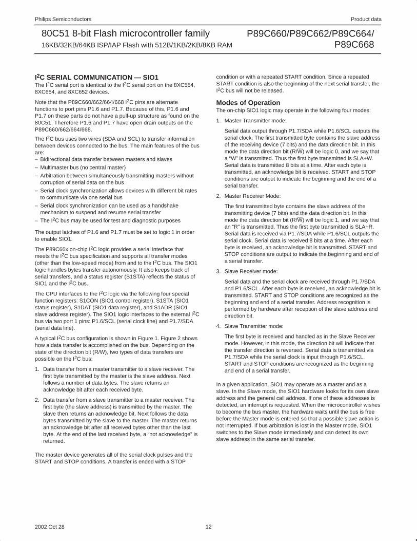
VDD
OTHER DEVICE WITHI2C INTERFACE
P89C66xOTHER DEVICE WITH
I2C INTERFACE
P1.7/SDA P1.6/SCL
SDA
SCLI2C bus
RPRP
SU01710
Figure 1. Typical I 2C Bus Configuration
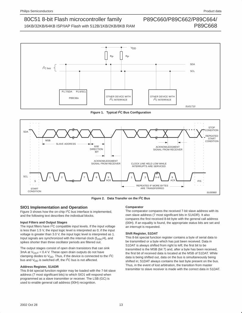
SCL
STARTCONDITION
S
SDA
P/S
MSB
ACKNOWLEDGMENTSIGNAL FROM RECEIVER
CLOCK LINE HELD LOW WHILEINTERRUPTS ARE SERVICED
1 2 7 8 9 1 2 3–8ACK
9ACK
REPEATED IF MORE BYTESARE TRANSFERRED
ACKNOWLEDGMENTSIGNAL FROM RECEIVER
SLAVE ADDRESSR/W
DIRECTION BIT
STOPCONDITION
REPEATEDSTART
CONDITION
SU00965
Figure 2. Data Transfer on the I 2C Bus
SIO1 Implementation and OperationFigure 3 shows how the on-chip I2C bus interface is implemented,and the following text describes the individual blocks.
Input Filters and Output StagesThe input filters have I2C compatible input levels. If the input voltageis less than 1.5 V, the input logic level is interpreted as 0; if the inputvoltage is greater than 3.0 V, the input logic level is interpreted as 1.Input signals are synchronized with the internal clock (fOSC/4), andspikes shorter than three oscillator periods are filtered out.
The output stages consist of open drain transistors that can sink3mA at VOUT < 0.4 V. These open drain outputs do not haveclamping diodes to VDD. Thus, if the device is connected to the I2Cbus and VDD is switched off, the I2C bus is not affected.
Address Register, S1ADRThis 8-bit special function register may be loaded with the 7-bit slaveaddress (7 most significant bits) to which SIO1 will respond whenprogrammed as a slave transmitter or receiver. The LSB (GC) isused to enable general call address (00H) recognition.
ComparatorThe comparator compares the received 7-bit slave address with itsown slave address (7 most significant bits in S1ADR). It alsocompares the first received 8-bit byte with the general call address(00H). If an equality is found, the appropriate status bits are set andan interrupt is requested.
Shift Register, S1DATThis 8-bit special function register contains a byte of serial data tobe transmitted or a byte which has just been received. Data inS1DAT is always shifted from right to left; the first bit to betransmitted is the MSB (bit 7) and, after a byte has been received,the first bit of received data is located at the MSB of S1DAT. Whiledata is being shifted out, data on the bus is simultaneously beingshifted in; S1DAT always contains the last byte present on the bus.Thus, in the event of lost arbitration, the transition from mastertransmitter to slave receiver is made with the correct data in S1DAT.

Philips Semiconductors Product data
P89C660/P89C662/P89C664/P89C668
80C51 8-bit Flash microcontroller family16KB/32KB/64KB ISP/IAP Flash with 512B/1KB/2KB/8KB RAM
2002 Oct 28 14
fOSC/4
INT
ER
NA
L B
US
ADDRESS REGISTER
COMPARATOR
SHIFT REGISTER
CONTROL REGISTER
STATUS REGISTER
ARBITRATION &SYNC LOGIC TIMING
&CONTROL
LOGIC
SERIAL CLOCKGENERATOR
ACK
STATUSDECODER
TIMER 1OVERFLOW
INTERRUPT
8
8
8
8
S1STA
STATUS BITS
S1CON
S1DAT
INPUTFILTER
OUTPUTSTAGE
P1.7
INPUTFILTER
OUTPUTSTAGE
P1.6
P1.6/SCL
P1.7/SDA
S1ADR
su00966
Figure 3. I 2C Bus Serial Interface Block Diagram

Philips Semiconductors Product data
P89C660/P89C662/P89C664/P89C668
80C51 8-bit Flash microcontroller family16KB/32KB/64KB ISP/IAP Flash with 512B/1KB/2KB/8KB RAM
2002 Oct 28 15
Arbitration and Synchronization LogicIn the Master Transmitter mode, the arbitration logic checks thatevery transmitted logic 1 actually appears as a logic 1 on the I2Cbus. If another device on the bus overrules a logic 1 and pulls theSDA line low, arbitration is lost, and SIO1 immediately changes frommaster transmitter to slave receiver. SIO1 will continue to outputclock pulses (on SCL) until transmission of the current serial byte iscomplete.
Arbitration may also be lost in the Master Receiver mode. Loss ofarbitration in this mode can only occur while SIO1 is returning a “notacknowledge: (logic 1) to the bus. Arbitration is lost when anotherdevice on the bus pulls this signal LOW. Since this can occur only atthe end of a serial byte, SIO1 generates no further clock pulses.Figure 4 shows the arbitration procedure.
The synchronization logic will synchronize the serial clock generatorwith the clock pulses on the SCL line from another device. If two ormore master devices generate clock pulses, the “mark” duration isdetermined by the device that generates the shortest “marks,” andthe “space” duration is determined by the device that generates thelongest “spaces.” Figure 5 shows the synchronization procedure.
A slave may stretch the space duration to slow down the busmaster. The space duration may also be stretched for handshakingpurposes. This can be done after each bit or after a complete bytetransfer. SIO1 will stretch the SCL space duration after a byte hasbeen transmitted or received and the acknowledge bit has beentransferred. The serial interrupt flag (SI) is set, and the stretchingcontinues until the serial interrupt flag is cleared.
ACK
1. Another device transmits identical serial data.
SDA
1 2 3 4 8 9SCL
(1) (1) (2)
(3)
2. Another device overrules a logic 1 (dotted line) transmitted by SIO1 (master) by pulling the SDA line low. Arbitration islost, and SIO1 enters the slave receiver mode.
3. SIO1 is in the slave receiver mode but still generates clock pulses until the current byte has been transmitted. SIO1 willnot generate clock pulses for the next byte. Data on SDA originates from the new master once it has won arbitration.
SU00967
Figure 4. Arbitration Procedure
(1)
SCL
(3) (1)
SDA
MARKDURATION
SPACE DURATION
(2)
1. Another service pulls the SCL line low before the SIO1 “mark” duration is complete. The serial clock generator is immediatelyreset and commences with the “space” duration by pulling SCL low.
2. Another device still pulls the SCL line low after SIO1 releases SCL. The serial clock generator is forced into the wait stateuntil the SCL line is released.
3. The SCL line is released, and the serial clock generator commences with the mark duration.SU00968
Figure 5. Serial Clock Synchronization

Philips Semiconductors Product data
P89C660/P89C662/P89C664/P89C668
80C51 8-bit Flash microcontroller family16KB/32KB/64KB ISP/IAP Flash with 512B/1KB/2KB/8KB RAM
2002 Oct 28 16
Serial Clock GeneratorThis programmable clock pulse generator provides the SCL clockpulses when SIO1 is in the Master Transmitter or Master Receivermode. It is switched off when SIO1 is in a Slave mode. Theprogrammable output clock frequencies are: fOSC/120, fOSC/9600(12-clock mode) or fOSC/60, fOSC/4800 (6-clock mode) and theTimer 1 overflow rate divided by eight. The output clock pulses havea 50% duty cycle unless the clock generator is synchronized withother SCL clock sources as described above.
Timing and ControlThe timing and control logic generates the timing and control signalsfor serial byte handling. This logic block provides the shift pulses forS1DAT, enables the comparator, generates and detects start andstop conditions, receives and transmits acknowledge bits, controlsthe master and Slave modes, contains interrupt request logic, andmonitors the I2C bus status.
Control Register, S1CONThis 7-bit special function register is used by the microcontroller tocontrol the following SIO1 functions: start and restart of a serialtransfer, termination of a serial transfer, bit rate, address recognition,and acknowledgment.
Status Decoder and Status RegisterThe status decoder takes all of the internal status bits andcompresses them into a 5-bit code. This code is unique for each I2Cbus status. The 5-bit code may be used to generate vectoraddresses for fast processing of the various service routines. Eachservice routine processes a particular bus status. There are 26possible bus states if all four modes of SIO1 are used. The 5-bitstatus code is latched into the five most significant bits of the statusregister when the serial interrupt flag is set (by hardware) andremains stable until the interrupt flag is cleared by software. Thethree least significant bits of the status register are always zero. Ifthe status code is used as a vector to service routines, then theroutines are displaced by eight address locations. Eight bytes ofcode is sufficient for most of the service routines.
The Four SIO1 Special Function RegistersThe microcontroller interfaces to SIO1 via four special functionregisters. These four SFRs (S1ADR, S1DAT, S1CON, and S1STA)are described individually in the following sections.
The Address Register, S1ADRThe CPU can read from and write to this 8-bit, directly addressableSFR. S1ADR is not affected by the SIO1 hardware. The contents ofthis register are irrelevant when SIO1 is in a Master mode. In theSlave modes, the seven most significant bits must be loaded withthe microcontroller’s own slave address, and, if the least significantbit is set, the general call address (00H) is recognized; otherwise itis ignored.
S1ADR (DBH) X GC
7 6 5 4 3 2 1 0
own slave address
X X X X X X
The most significant bit corresponds to the first bit received from theI2C bus after a start condition. A logic 1 in S1ADR corresponds to ahigh level on the I2C bus, and a logic 0 corresponds to a low levelon the bus.
The Data Register, S1DATS1DAT contains a byte of serial data to be transmitted or a bytewhich has just been received. The CPU can read from and write to
this 8-bit, directly addressable SFR while it is not in the process ofshifting a byte. This occurs when SIO1 is in a defined state and theserial interrupt flag is set. Data in S1DAT remains stable as long asSI is set. Data in S1DAT is always shifted from right to left: the firstbit to be transmitted is the MSB (bit 7), and, after a byte has beenreceived, the first bit of received data is located at the MSB ofS1DAT. While data is being shifted out, data on the bus issimultaneously being shifted in; S1DAT always contains the lastdata byte present on the bus. Thus, in the event of lost arbitration,the transition from master transmitter to slave receiver is made withthe correct data in S1DAT.
S1DAT (DAH) SD7 SD6 SD5 SD4 SD3 SD2 SD1 SD0
7 6 5 4 3 2 1 0
shift direction
SD7 - SD0:Eight bits to be transmitted or just received. A logic 1 in S1DATcorresponds to a high level on the I2C bus, and a logic 0corresponds to a low level on the bus. Serial data shifts throughS1DAT from right to left. Figure 6 shows how data in S1DAT isserially transferred to and from the SDA line.
S1DAT and the ACK flag form a 9-bit shift register which shifts in orshifts out an 8-bit byte, followed by an acknowledge bit. The ACKflag is controlled by the SIO1 hardware and cannot be accessed bythe CPU. Serial data is shifted through the ACK flag into S1DAT onthe rising edges of serial clock pulses on the SCL line. When a bytehas been shifted into S1DAT, the serial data is available in S1DAT,and the acknowledge bit is returned by the control logic during theninth clock pulse. Serial data is shifted out from S1DAT via a buffer(BSD7) on the falling edges of clock pulses on the SCL line.
When the CPU writes to S1DAT, BSD7 is loaded with the content ofS1DAT.7, which is the first bit to be transmitted to the SDA line (seeFigure 7). After nine serial clock pulses, the eight bits in S1DAT willhave been transmitted to the SDA line, and the acknowledge bit willbe present in ACK. Note that the eight transmitted bits are shiftedback into S1DAT.
The Control Register, S1CONThe CPU can read from and write to this 8-bit, directly addressableSFR. Two bits are affected by the SIO1 hardware: the SI bit is setwhen a serial interrupt is requested, and the STO bit is cleared whena STOP condition is present on the I2C bus. The STO bit is alsocleared when ENS1 = “0”.
S1CON (D8H) ENS1 STA STO SI AA CR1 CR0
7 6 5 4 3 2 1 0
CR2
ENS1, the SIO1 Enable Bit: ENS1 = “0”: When ENS1 is “0”, theSDA and SCL outputs are in a high impedance state. SDA and SCLinput signals are ignored, SIO1 is in the “not addressed” slave state,and the STO bit in S1CON is forced to “0”. No other bits areaffected. P1.6 and P1.7 may be used as open drain I/O ports.
ENS1 = “1”: When ENS1 is “1”, SIO1 is enabled. The P1.6 and P1.7port latches must be set to logic 1.
ENS1 should not be used to temporarily release SIO1 from the I2Cbus since, when ENS1 is reset, the I2C bus status is lost. The AAflag should be used instead (see description of the AA flag in thefollowing text).

Philips Semiconductors Product data
P89C660/P89C662/P89C664/P89C668
80C51 8-bit Flash microcontroller family16KB/32KB/64KB ISP/IAP Flash with 512B/1KB/2KB/8KB RAM
2002 Oct 28 17
INTERNAL BUS
8
BSD7 S1DAT ACK
SCL
SDA
SHIFT PULSES
SU00969
Figure 6. Serial Input/Output Configuration
SHIFT IN
SDA
SCL
D7 D6 D5 D4 D3 D2 D1 D0 A
SHIFT ACK & S1DAT
ACK (2) (2) (2) (2) (2) (2) (2) (2) A
(2) (2) (2) (2) (2) (2) (2) (2) (1)(1)S1DAT
SHIFT BSD7
BSD7 D7 D6 D5 D4 D3 D2 D1 D0 (3)
LOADED BY THE CPU
(1) Valid data in S1DAT
(2) Shifting data in S1DAT and ACK
(3) High level on SDA
SHIFT OUT
SU00970
Figure 7. Shift-in and Shift-out Timing
In the following text, it is assumed that ENS1 = “1”.
The “START” Flag, STA: STA = “1”: When the STA bit is set toenter a Master mode, the SIO1 hardware checks the status of theI2C bus and generates a START condition if the bus is free. If thebus is not free, then SIO1 waits for a STOP condition (which will freethe bus) and generates a START condition after a delay of half aclock period of the internal serial clock generator.
If STA is set while SIO1 is already in a Master mode and one ormore bytes are transmitted or received, SIO1 transmits a repeatedSTART condition. STA may be set at any time. STA may also be setwhen SIO1 is an addressed slave.
STA = “0”: When the STA bit is reset, no START condition orrepeated START condition will be generated.
The STOP Flag, STO: STO = “1”: When the STO bit is set whileSIO1 is in a Master mode, a STOP condition is transmitted to theI2C bus. When the STOP condition is detected on the bus, the SIO1hardware clears the STO flag. In a Slave mode, the STO flag maybe set to recover from an error condition. In this case, no STOPcondition is transmitted to the I2C bus. However, the SIO1 hardwarebehaves as if a STOP condition has been received and switches tothe defined “not addressed” Slave Receiver mode. The STO flag isautomatically cleared by hardware.

Philips Semiconductors Product data
P89C660/P89C662/P89C664/P89C668
80C51 8-bit Flash microcontroller family16KB/32KB/64KB ISP/IAP Flash with 512B/1KB/2KB/8KB RAM
2002 Oct 28 18
If the STA and STO bits are both set, the a STOP condition istransmitted to the I2C bus if SIO1 is in a Master mode (in a Slavemode, SIO1 generates an internal STOP condition which is nottransmitted). SIO1 then transmits a START condition.
STO = “0”: When the STO bit is reset, no STOP condition will begenerated.
The Serial Interrupt Flag, SI: SI = “1”: When the SI flag is set, then,if the EA and ES1 (interrupt enable register) bits are also set, aserial interrupt is requested. SI is set by hardware when one of 25 ofthe 26 possible SIO1 states is entered. The only state that does notcause SI to be set is state F8H, which indicates that no relevantstate information is available.
While SI is set, the low period of the serial clock on the SCL line isstretched, and the serial transfer is suspended. A high level on theSCL line is unaffected by the serial interrupt flag. SI must be resetby software.
SI = “0”: When the SI flag is reset, no serial interrupt is requested,and there is no stretching of the serial clock on the SCL line.
The Assert Acknowledge Flag, AA: AA = “1”: If the AA flag is set,an acknowledge (low level to SDA) will be returned during theacknowledge clock pulse on the SCL line when:– The “own slave address” has been received
– The general call address has been received while the general callbit (GC) in S1ADR is set
– A data byte has been received while SIO1 is in the MasterReceiver mode
– A data byte has been received while SIO1 is in the addressedSlave Receiver mode
AA = “0”: if the AA flag is reset, a not acknowledge (high level toSDA) will be returned during the acknowledge clock pulse on SCLwhen:– A data has been received while SIO1 is in the Master Receiver
mode
– A data byte has been received while SIO1 is in the addressedSlave Receiver mode
When SIO1 is in the addressed Slave Transmitter mode, state C8Hwill be entered after the last serial is transmitted (see Figure 11).
When SI is cleared, SIO1 leaves state C8H, enters the notaddressed Slave Receiver mode, and the SDA line remains at ahigh level. In state C8H, the AA flag can be set again for futureaddress recognition.
When SIO1 is in the not addressed Slave mode, its own slaveaddress and the general call address are ignored. Consequently, noacknowledge is returned, and a serial interrupt is not requested.Thus, SIO1 can be temporarily released from the I2C bus while thebus status is monitored. While SIO1 is released from the bus,START and STOP conditions are detected, and serial data is shiftedin. Address recognition can be resumed at any time by setting theAA flag. If the AA flag is set when the part’s own Slave address orthe general call address has been partly received, the address willbe recognized at the end of the byte transmission.
The Clock Rate Bits CR0, CR1, and CR2: These three bitsdetermine the serial clock frequency when SIO1 is in a Mastermode. The various serial rates are shown in Table 3.
A 12.5 kHz bit rate may be used by devices that interface to the I2Cbus via standard I/O port lines which are software driven and slow.100 kHz is usually the maximum bit rate and can be derived from a16 MHz, 12 MHz, or a 6 MHz oscillator. A variable bit rate (0.5 kHzto 62.5 kHz) may also be used if Timer 1 is not required for anyother purpose while SIO1 is in a Master mode.
The frequencies shown in Table 3 are unimportant when SIO1 is in aSlave mode. In the Slave modes, SIO1 will automaticallysynchronize with any clock frequency up to 100 kHz.
The Status Register, S1STAS1STA is an 8-bit read-only special function register. The three leastsignificant bits are always zero. The five most significant bits containthe status code. There are 26 possible status codes. When S1STAcontains F8H, no relevant state information is available and no serialinterrupt is requested. All other S1STA values correspond to definedSIO1 states. When each of these states is entered, a serial interruptis requested (SI = “1”). A valid status code is present in S1STA onemachine cycle after SI is set by hardware and is still present onemachine cycle after SI has been reset by software.

Philips Semiconductors Product data
P89C660/P89C662/P89C664/P89C668
80C51 8-bit Flash microcontroller family16KB/32KB/64KB ISP/IAP Flash with 512B/1KB/2KB/8KB RAM
2002 Oct 28 19
Table 3. Serial Clock Rates
6-clock modeBIT FREQUENCY (kHz) AT f OSC
CR2 CR1 CR0 3 MHz 6 MHz 8 MHz 12 MHz2 15 MHz2 fOSC DIVIDED BY
0 0 0 23 47 62.5 94 1171 1280 0 1 27 54 71 1071 1341 1120 1 0 31 63 83.3 1251 1561 960 1 1 37 75 100 1501 1881 801 0 0 6.25 12.5 17 25 31 4801 0 1 50 100 1331 2001 2501 601 1 0 100 200 2671 4001 5001 301 1 1 0.24 < 62.5
0 < 2550.49 < 62.5
0 < 2540.65 < 55.6
0 < 2530.98 < 50.0
0 < 2511.22 < 52.1
0 < 25048 × (256 – (reload value Timer 1))Reload value Timer 1 in Mode 2.
12-clock modeBIT FREQUENCY (kHz) AT f OSC
CR2 CR1 CR0 6 MHz 12 MHz 16 MHz 24 MHz3 30 MHz3 fOSC DIVIDED BY
0 0 0 23 47 62.5 94 1171 2560 0 1 27 54 71 1071 1341 2240 1 0 31 63 83.3 1251 1561 1920 1 1 37 75 100 1501 1881 1601 0 0 6.25 12.5 17 25 31 9601 0 1 50 100 1331 2001 2501 1201 1 0 100 200 2671 4001 5001 601 1 1 0.24 < 62.5
0 < 2550.49 < 62.5
0 < 2540.65 < 55.6
0 < 2530.98 < 50.0
0 < 2511.22 < 52.1
0 < 25096 × (256 – (reload value Timer 1))Reload value Timer 1 in Mode 2.
NOTES:1. These frequencies exceed the upper limit of 100 kHz of the I2C-bus specification and cannot be used in an I2C-bus application.2. At fOSC = 12 MHz/15 MHz the maximum I2C bus rate of 100 kHz cannot be realized due to the fixed divider rates.3. At fOSC = 24 MHz/30 MHz the maximum I2C bus rate of 100 kHz cannot be realized due to the fixed divider rates.

Philips Semiconductors Product data
P89C660/P89C662/P89C664/P89C668
80C51 8-bit Flash microcontroller family16KB/32KB/64KB ISP/IAP Flash with 512B/1KB/2KB/8KB RAM
2002 Oct 28 20
More Information on SIO1 Operating ModesThe four operating modes are:– Master Transmitter
– Master Receiver
– Slave Receiver
– Slave Transmitter
Data transfers in each mode of operation are shown in Figures 8-11.These figures contain the following abbreviations:
Abbreviation ExplanationS Start conditionSLA 7-bit slave addressR Read bit (high level at SDA)W Write bit (low level at SDA)A Acknowledge bit (low level at SDA)A Not acknowledge bit (high level at SDA)Data 8-bit data byteP Stop condition
In Figures 8-11, circles are used to indicate when the serial interruptflag is set. The numbers in the circles show the status code held inthe S1STA register. At these points, a service routine must beexecuted to continue or complete the serial transfer. These serviceroutines are not critical since the serial transfer is suspended untilthe serial interrupt flag is cleared by software.
When a serial interrupt routine is entered, the status code in S1STAis used to branch to the appropriate service routine. For each statuscode, the required software action and details of the following serialtransfer are given in Tables 4-8.
Master Transmitter modeIn the Master Transmitter mode, a number of data bytes aretransmitted to a slave receiver (see Figure 8). Before the MasterTransmitter mode can be entered, S1CON must be initialized asfollows:
S1CON (D8H) CR2 ENS1 STA STO SI AA CR1 CR0
7 6 5 4 3 2 1 0
1 0 0 0 X bit ratebitrate
CR0, CR1, and CR2 define the serial bit rate. ENS1 must be set tologic 1 to enable SIO1. If the AA bit is reset, SIO1 will notacknowledge its own slave address or the general call address inthe event of another device becoming master of the bus. In otherwords, if AA is reset, SIO0 cannot enter a Slave mode. STA, STO,and SI must be reset.
The Master Transmitter mode may now be entered by setting theSTA bit using the SETB instruction. The SIO1 logic will now test theI2C bus and generate a start condition as soon as the bus becomesfree. When a START condition is transmitted, the serial interrupt flag(SI) is set, and the status code in the status register (S1STA) will be08H. This status code must be used to vector to an interrupt serviceroutine that loads S1DAT with the slave address and the datadirection bit (SLA+W). The SI bit in S1CON must then be resetbefore the serial transfer can continue.
When the slave address and the direction bit have been transmittedand an acknowledgment bit has been received, the serial interruptflag (SI) is set again, and a number of status codes in S1STA arepossible. There are 18H, 20H, or 38H for the Master mode and also68H, 78H, or B0H if the Slave mode was enabled (AA = logic 1). Theappropriate action to be taken for each of these status codes isdetailed in Table 4. After a repeated start condition (state 10H). SIO1
may switch to the Master Receiver mode by loading S1DAT withSLA+R).
Master Receiver modeIn the Master Receiver mode, a number of data bytes are receivedfrom a slave transmitter (see Figure 9). The transfer is initialized asin the Master Transmitter mode. When the start condition has beentransmitted, the interrupt service routine must load S1DAT with the7-bit slave address and the data direction bit (SLA+R). The SI bit inS1CON must then be cleared before the serial transfer cancontinue.
When the slave address and the data direction bit have beentransmitted and an acknowledgment bit has been received, theserial interrupt flag (SI) is set again, and a number of status codes inS1STA are possible. These are 40H, 48H, or 38H for the Mastermode and also 68H, 78H, or B0H if the Slave mode was enabled(AA = logic 1). The appropriate action to be taken for each of thesestatus codes is detailed in Table 5. ENS1, CR1, and CR0 are notaffected by the serial transfer and are not referred to in Table 5. Aftera repeated start condition (state 10H), SIO1 may switch to theMaster Transmitter mode by loading S1DAT with SLA+W.
Slave Receiver modeIn the Slave Receiver mode, a number of data bytes are receivedfrom a master transmitter (see Figure 10). To initiate the SlaveReceiver mode, S1ADR and S1CON must be loaded as follows:
S1ADR (DBH) X GC
7 6 5 4 3 2 1 0
own slave address
X X X X X X
The upper 7 bits are the address to which SIO1 will respond whenaddressed by a master. If the LSB (GC) is set, SIO1 will respond tothe general call address (00H); otherwise it ignores the general calladdress.
S1CON (D8H) ENS1 STA STO SI AA CR1 CR0
7 6 5 4 3 2 1 0
X 1 0 0 0 1 X X
CR2
CR0, CR1, and CR2 do not affect SIO1 in the Slave mode. ENS1must be set to logic 1 to enable SIO1. The AA bit must be set toenable SIO1 to acknowledge its own slave address or the generalcall address. STA, STO, and SI must be reset.
When S1ADR and S1CON have been initialized, SIO1 waits until itis addressed by its own slave address followed by the data directionbit which must be “0” (W) for SIO1 to operate in the Slave Receivermode. After its own slave address and the W bit have beenreceived, the serial interrupt flag (I) is set and a valid status codecan be read from S1STA. This status code is used to vector to aninterrupt service routine, and the appropriate action to be taken foreach of these status codes is detailed in Table 6. The SlaveReceiver mode may also be entered if arbitration is lost while SIO1is in the Master mode (see status 68H and 78H).
If the AA bit is reset during a transfer, SIO1 will return a notacknowledge (logic 1) to SDA after the next received data byte.While AA is reset, SIO1 does not respond to its own slave addressor a general call address. However, the I2C bus is still monitoredand address recognition may be resumed at any time by setting AA.This means that the AA bit may be used to temporarily isolate SIO1from the I2C bus.

Philips Semiconductors Product data
P89C660/P89C662/P89C664/P89C668
80C51 8-bit Flash microcontroller family16KB/32KB/64KB ISP/IAP Flash with 512B/1KB/2KB/8KB RAM
2002 Oct 28 21
ÇÇÇÇÇÇÇÇÇÇÇÇÇÇÇÇ
ÇÇÇÇÇÇÇÇÇÇÇÇ
ÇÇÇÇÇÇ
S SLA W A ADATA P
ÇÇÇÇÇÇÇÇÇÇÇÇÇÇÇÇÇÇÇÇÇ
S SLA W
ÇÇÇÇÇÇ
A P
ÇÇÇÇÇÇÇÇÇ
A P
08H 18H 28H
ÇÇÇÇÇÇ
R
38H
A or AOTHER MSTCONTINUES A or A
OTHER MSTCONTINUES
38H
30H
20H
68H 78H 80H
OTHER MSTCONTINUES
A
MT
10H
TO MST/REC MODEENTRY = MR
TO CORRESPONDINGSTATES IN SLAVE MODE
SUCCESSFUL TRANSMISSIONTO A SLAVE RECEIVER
NEXT TRANSFER STARTED WITH A REPEATED START CONDITION
NOT ACKNOWLEDGE RECEIVED AFTER THE SLAVE ADDRESS
NOT ACKNOWLEDGE RECEIVED AFTER A DATA BYTE
ARBITRATION LOST IN SLAVE ADDRESS OR DATA BYTE
ARBITRATION LOST AND ADDRESSED AS SLAVE
ÇÇÇÇÇÇÇÇÇÇÇÇÇÇÇÇÇÇÇÇÇÇÇÇÇ
ÇÇÇÇÇÇ
A
n
FROM MASTER TO SLAVE
FROM SLAVE TO MASTER
ANY NUMBER OF DATA BYTES AND THEIR ASSOCIATED ACKNOWLEDGE BITS
THIS NUMBER (CONTAINED IN S1STA) CORRESPONDS TO A DEFINED STATE OF THE I2C BUS. SEE TABLE 4.
Data
SU00971
Figure 8. Format and States in the Master Transmitter mode

Philips Semiconductors Product data
P89C660/P89C662/P89C664/P89C668
80C51 8-bit Flash microcontroller family16KB/32KB/64KB ISP/IAP Flash with 512B/1KB/2KB/8KB RAM
2002 Oct 28 22
ÇÇÇÇÇÇÇÇÇÇÇÇÇÇÇÇ
ÇÇÇÇÇÇ
S SLA R A DATA P
ÇÇÇÇÇÇÇÇÇÇÇÇÇÇÇÇÇÇÇÇÇ
S SLA R
ÇÇÇÇÇÇA P
08H 40H 50H
ÇÇÇÇÇÇ
W
38H
A or AOTHER MSTCONTINUES
OTHER MSTCONTINUES
38H
48H
68H 78H 80H
OTHER MSTCONTINUES
A
MR
10H
TO MST/TRX MODEENTRY = MT
TO CORRESPONDINGSTATES IN SLAVE MODE
SUCCESSFUL RECEPTIONFROM A SLAVE TRANSMITTER
NEXT TRANSFER STARTED WITH AREPEATED START CONDITION
NOT ACKNOWLEDGE RECEIVEDAFTER THE SLAVE ADDRESS
ARBITRATION LOST IN SLAVE ADDRESSOR ACKNOWLEDGE BIT
ARBITRATION LOST AND ADDRESSED AS SLAVE
ÇÇÇÇÇÇÇÇÇÇÇÇÇÇÇÇÇÇÇÇ
n
FROM MASTER TO SLAVE
FROM SLAVE TO MASTER
ANY NUMBER OF DATA BYTES AND THEIR ASSOCIATED ACKNOWLEDGE BITS
THIS NUMBER (CONTAINED IN S1STA) CORRESPONDS TO A DEFINED STATE OF THE I2C BUS. SEE TABLE 5.
ÇÇÇÇÇÇ
AÇÇÇÇÇÇÇÇ
DATAÇÇÇÇÇÇ
A
58H
ÇÇÇÇÇÇÇÇÇ
A
ÇÇÇÇ
DATA A
SU00972
Figure 9. Format and States in the Master Receiver Mode

Philips Semiconductors Product data
P89C660/P89C662/P89C664/P89C668
80C51 8-bit Flash microcontroller family16KB/32KB/64KB ISP/IAP Flash with 512B/1KB/2KB/8KB RAM
2002 Oct 28 23
ÇÇÇÇÇÇÇÇÇÇÇÇÇÇ
ÇÇÇÇÇÇÇÇÇÇÇÇÇÇ
ÇÇÇÇÇÇ
S SLA W A ADATA P or S
A
60H 80H
68H
RECEPTION OF THE OWN SLAVE ADDRESSAND ONE OR MORE DATA BYTESALL ARE ACKNOWLEDGED.
LAST DATA BYTE RECEIVED ISNOT ACKNOWLEDGED
ARBITRATION LOST AS MST ANDADDRESSED AS SLAVE
RECEPTION OF THE GENERAL CALL ADDRESSAND ONE OR MORE DATA BYTES
LAST DATA BYTE IS NOT ACKNOWLEDGED
ARBITRATION LOST AS MST AND ADDRESSED AS SLAVE BY GENERAL CALL
ÇÇÇÇÇÇÇÇÇÇÇÇÇÇÇÇÇÇÇÇÇÇÇÇÇ
ÇÇÇÇÇÇ
A
n
FROM MASTER TO SLAVE
FROM SLAVE TO MASTER
ANY NUMBER OF DATA BYTES AND THEIR ASSOCIATED ACKNOWLEDGE BITS
THIS NUMBER (CONTAINED IN S1STA) CORRESPONDS TO A DEFINED STATE OF THE I2C BUS. SEE TABLE 6.
Data
A SLAÇÇÇÇÇÇ
DATA
80H A0H
ÇÇÇÇÇÇÇÇÇ
A
88H
P or S
ÇÇÇÇÇÇÇÇÇÇÇÇÇÇÇ
ÇÇÇÇÇÇÇÇÇ
ÇÇÇÇÇÇÇÇÇÇÇÇ
ÇÇÇÇÇÇÇÇÇ
ÇÇÇÇÇÇÇÇÇ
ÇÇÇÇÇÇÇÇÇ
GENERALCALL A ADATA P or S
70H 90H
78H
A DATA
90H A0H
A
98H
P or S
A
SU00973
Figure 10. Format and States in the Slave Receiver mode
Philips Semiconductors Product data
P89C660/P89C662/P89C664/P89C668
80C51 8-bit Flash microcontroller family16KB/32KB/64KB ISP/IAP Flash with 512B/1KB/2KB/8KB RAM
2002 Oct 28 24
ÇÇÇÇÇÇÇÇÇÇÇÇÇÇÇÇÇÇÇÇÇÇÇÇ
ÇÇÇÇÇÇÇÇÇ
ÇÇÇÇÇÇÇÇÇ
ÇÇÇÇÇÇÇÇÇÇÇÇ
ÇÇÇÇÇÇÇÇÇ
S SLA R A DATA P or S
B0H
A8H B8H
RECEPTION OF THEOWN SLAVE ADDRESSAND TRANSMISSIONOF ONE OR MOREDATA BYTES
ADATAA
C0H
ÇÇÇÇÇÇÇÇ
ÇÇÇÇ
n
ANY NUMBER OF DATA BYTES AND THEIR ASSOCIATED ACKNOWLEDGE BITS
THIS NUMBER (CONTAINED IN S1STA) CORRESPONDS TO A DEFINED STATE OF THE I2C BUS. SEE TABLE 7.
DATA A
ÇÇÇÇÇÇÇÇÇ
All “1”s
ÇÇÇÇÇÇÇÇÇ
A
A
ÇÇÇÇÇÇÇÇ
FROM MASTER TO SLAVE
FROM SLAVE TO MASTER
C8H
P or SLAST DATA BYTE TRANSMITTED.SWITCHED TO NOT ADDRESSEDSLAVE (AA BIT IN S1CON = “0”
ARBITRATION LOST AS MSTAND ADDRESSED AS SLAVE
SU00974
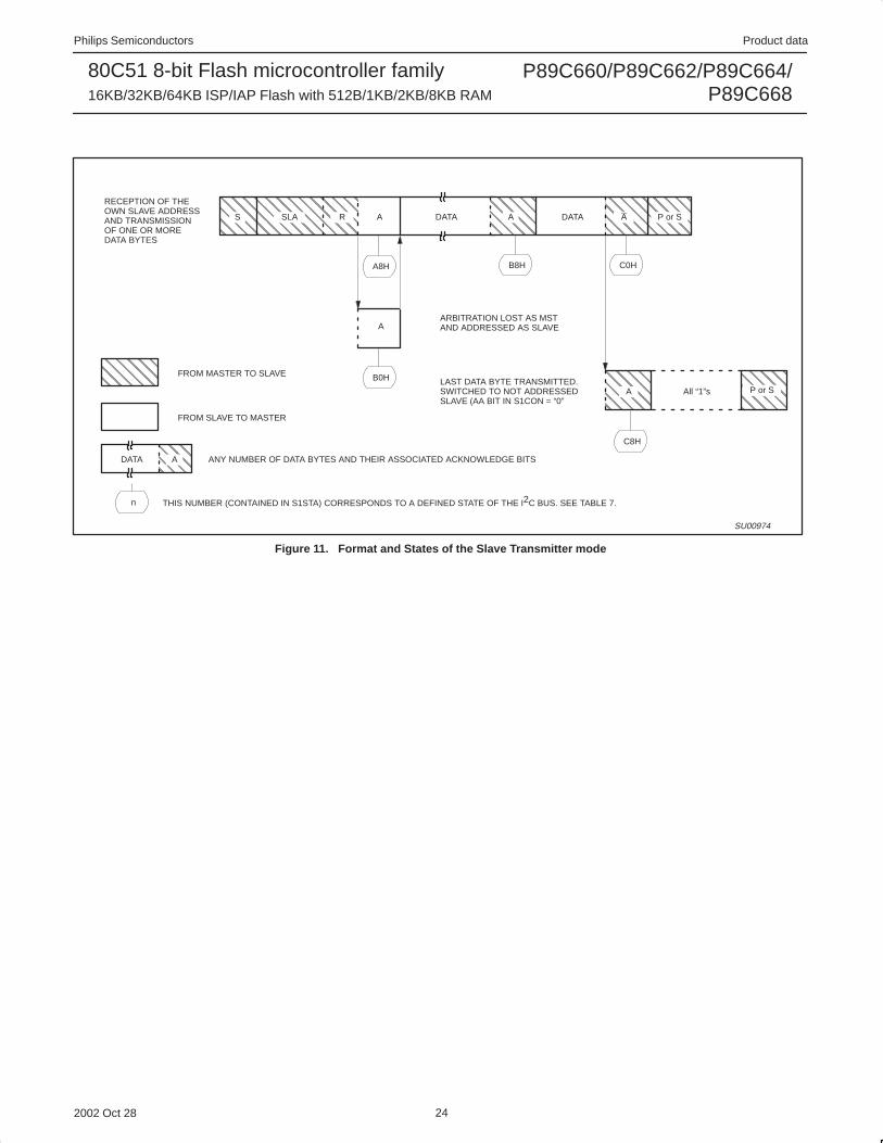
Figure 11. Format and States of the Slave Transmitter mode

Philips Semiconductors Product data
P89C660/P89C662/P89C664/P89C668
80C51 8-bit Flash microcontroller family16KB/32KB/64KB ISP/IAP Flash with 512B/1KB/2KB/8KB RAM
2002 Oct 28 25
Table 4. Master Transmitter mode
STATUS STATUS OF THEAPPLICATION SOFTWARE RESPONSE
STATUSCODE
(S1STA)
STATUS OF THEI2C BUS AND
SIO1 HARDWARE TO/FROM S1DATTO S1CON NEXT ACTION TAKEN BY SIO1 HARDWARE
(S1STA) SIO1 HARDWARE TO/FROM S1DATSTA STO SI AA
08H A START condition hasbeen transmitted
Load SLA+W X 0 0 X SLA+W will be transmitted;ACK bit will be received
10H A repeated STARTditi h b
Load SLA+W or X 0 0 X As abovecondition has beentransmitted
Load SLA+R X 0 0 X SLA+W will be transmitted;SIO1 will be switched to MST/REC mode
18H SLA+W has been transmitted; ACK hasb i d
Load data byte or 0 0 0 X Data byte will be transmitted;ACK bit will be received
been received no S1DAT action or 1 0 0 X Repeated START will be transmitted;no S1DAT action or 0 1 0 X STOP condition will be transmitted;
STO flag will be resetno S1DAT action 1 1 0 X STOP condition followed by a
START condition will be transmitted;STO flag will be reset
20H SLA+W has been transmitted; NOT ACKh b i d
Load data byte or 0 0 0 X Data byte will be transmitted;ACK bit will be received
has been received no S1DAT action or 1 0 0 X Repeated START will be transmitted;no S1DAT action or 0 1 0 X STOP condition will be transmitted;
STO flag will be resetno S1DAT action 1 1 0 X STOP condition followed by a
START condition will be transmitted;STO flag will be reset
28H Data byte in S1DAT hasbeen transmitted; ACKh b i d
Load data byte or 0 0 0 X Data byte will be transmitted;ACK bit will be received
has been received no S1DAT action or 1 0 0 X Repeated START will be transmitted;no S1DAT action or 0 1 0 X STOP condition will be transmitted;
STO flag will be resetno S1DAT action 1 1 0 X STOP condition followed by a
START condition will be transmitted;STO flag will be reset
30H Data byte in S1DAT hasbeen transmitted; NOTACK h b i d
Load data byte or 0 0 0 X Data byte will be transmitted;ACK bit will be received
ACK has been received no S1DAT action or 1 0 0 X Repeated START will be transmitted;no S1DAT action or 0 1 0 X STOP condition will be transmitted;
STO flag will be resetno S1DAT action 1 1 0 X STOP condition followed by a
START condition will be transmitted;STO flag will be reset
38H Arbitration lost in SLA+R/W orD b
No S1DAT action or 0 0 0 X I2C bus will be released;not addressed slave will be entered
Data bytes No S1DAT action 1 0 0 X A START condition will be transmitted when thebus becomes free

Philips Semiconductors Product data
P89C660/P89C662/P89C664/P89C668
80C51 8-bit Flash microcontroller family16KB/32KB/64KB ISP/IAP Flash with 512B/1KB/2KB/8KB RAM
2002 Oct 28 26
Table 5. Master Receiver Mode
STATUS STATUS OF THE I2CAPPLICATION SOFTWARE RESPONSE
STATUSCODE
(S1STA)
STATUS OF THE I2CBUS AND
SIO1 HARDWARE TO/FROM S1DATTO S1CON NEXT ACTION TAKEN BY SIO1 HARDWARE
(S1STA) SIO1 HARDWARE TO/FROM S1DATSTA STO SI AA
08H A START condition hasbeen transmitted
Load SLA+R X 0 0 X SLA+R will be transmitted;ACK bit will be received
10H A repeated STARTditi h b
Load SLA+R or X 0 0 X As abovecondition has been transmitted
Load SLA+W X 0 0 X SLA+W will be transmitted;SIO1 will be switched to MST/TRX mode
38H Arbitration lost in NOT ACK bit
No S1DAT action or 0 0 0 X I2C bus will be released;SIO1 will enter a Slave mode
No S1DAT action 1 0 0 X A START condition will be transmitted when thebus becomes free
40H SLA+R has been transmitted; ACK hasb i d
No S1DAT action or 0 0 0 0 Data byte will be received;NOT ACK bit will be returned
been received no S1DAT action 0 0 0 1 Data byte will be received;ACK bit will be returned
48H SLA+R has been t itt d NOT ACK
No S1DAT action or 1 0 0 X Repeated START condition will be transmittedtransmitted; NOT ACKhas been received
no S1DAT action or 0 1 0 X STOP condition will be transmitted;STO flag will be reset
no S1DAT action 1 1 0 X STOP condition followed by a START condition will be transmitted;STO flag will be reset
50H Data byte has been received; ACK has been
d
Read data byte or 0 0 0 0 Data byte will be received;NOT ACK bit will be returned
returned read data byte 0 0 0 1 Data byte will be received;ACK bit will be returned
58H Data byte has been i d NOT ACK h
Read data byte or 1 0 0 X Repeated START condition will be transmittedreceived; NOT ACK hasbeen returned
read data byte or 0 1 0 X STOP condition will be transmitted;STO flag will be reset
read data byte 1 1 0 X STOP condition followed by a START condition will be transmitted;STO flag will be reset

Philips Semiconductors Product data
P89C660/P89C662/P89C664/P89C668
80C51 8-bit Flash microcontroller family16KB/32KB/64KB ISP/IAP Flash with 512B/1KB/2KB/8KB RAM
2002 Oct 28 27
Table 6. Slave Receiver mode
STATUS STATUS OF THEAPPLICATION SOFTWARE RESPONSE
STATUSCODE
(S1STA)
STATUS OF THEI2C BUS AND
SIO1 HARDWARE TO/FROM S1DATTO S1CON NEXT ACTION TAKEN BY SIO1 HARDWARE
(S1STA) SIO1 HARDWARE TO/FROM S1DATSTA STO SI AA
60H Own SLA+W hasbeen received; ACKh b d
No S1DAT action or X 0 0 0 Data byte will be received and NOT ACK will bereturned
has been returned no S1DAT action X 0 0 1 Data byte will be received and ACK will be returned
68H Arbitration lost inSLA+R/W as master;Own SLA+W hasb i d ACK
No S1DAT action or X 0 0 0 Data byte will be received and NOT ACK will bereturned
been received, ACKreturned
no S1DAT action X 0 0 1 Data byte will be received and ACK will be returned
70H General call address(00H) has beenreceived; ACK has
No S1DAT action or X 0 0 0 Data byte will be received and NOT ACK will bereturned
received ACK hasbeen returned no S1DAT action X 0 0 1 Data byte will be received and ACK will be returned
78H Arbitration lost inSLA+R/W as master;General call addresshas been received
No S1DAT action or X 0 0 0 Data byte will be received and NOT ACK will bereturned
has been received,ACK has beenreturned
no S1DAT action X 0 0 1 Data byte will be received and ACK will be returned
80H Previously addressedwith own SLVaddress; DATA hasb i d ACK
Read data byte or X 0 0 0 Data byte will be received and NOT ACK will bereturned
been received; ACKhas been returned
read data byte X 0 0 1 Data byte will be received and ACK will be returned
88H Previously addressedwith own SLA; DATAb h b
Read data byte or 0 0 0 0 Switched to not addressed SLV mode; no recognitionof own SLA or General call address
byte has beenreceived; NOT ACKhas been returned
read data byte or 0 0 0 1 Switched to not addressed SLV mode; Own SLA willbe recognized; General call address will berecognized if S1ADR.0 = logic 1
read data byte or 1 0 0 0 Switched to not addressed SLV mode; no recognitionof own SLA or General call address. A STARTcondition will be transmitted when the bus becomesfree
read data byte 1 0 0 1 Switched to not addressed SLV mode; Own SLA willbe recognized; General call address will berecognized if S1ADR.0 = logic 1. A START conditionwill be transmitted when the bus becomes free.
90H Previously addressedwith General Call;DATA byte has been
i d ACK h
Read data byte or X 0 0 0 Data byte will be received and NOT ACK will bereturned
received; ACK hasbeen returned
read data byte X 0 0 1 Data byte will be received and ACK will be returned
98H Previously addressedwith General Call;DATA b h b
Read data byte or 0 0 0 0 Switched to not addressed SLV mode; no recognitionof own SLA or General call address
DATA byte has beenreceived; NOT ACKhas been returned
read data byte or 0 0 0 1 Switched to not addressed SLV mode; Own SLA willbe recognized; General call address will berecognized if S1ADR.0 = logic 1
read data byte or 1 0 0 0 Switched to not addressed SLV mode; no recognitionof own SLA or General call address. A STARTcondition will be transmitted when the bus becomesfree
read data byte 1 0 0 1 Switched to not addressed SLV mode; Own SLA willbe recognized; General call address will berecognized if S1ADR.0 = logic 1. A START conditionwill be transmitted when the bus becomes free.

Philips Semiconductors Product data
P89C660/P89C662/P89C664/P89C668
80C51 8-bit Flash microcontroller family16KB/32KB/64KB ISP/IAP Flash with 512B/1KB/2KB/8KB RAM
2002 Oct 28 28
Table 6. Slave Receiver mode (Continued)
STATUS STATUS OF THEAPPLICATION SOFTWARE RESPONSE
STATUSCODE
(S1STA)
STATUS OF THEI2C BUS AND
SIO1 HARDWARE TO/FROM S1DATTO S1CON NEXT ACTION TAKEN BY SIO1 HARDWARE
(S1STA) SIO1 HARDWARE TO/FROM S1DATSTA STO SI AA
A0H A STOP condition orrepeated START
di i h b
No STDAT action or 0 0 0 0 Switched to not addressed SLV mode; no recognitionof own SLA or General call address
condition has beenreceived while stilladdressed asSLV/REC or SLV/TRX
No STDAT action or 0 0 0 1 Switched to not addressed SLV mode; Own SLA willbe recognized; General call address will berecognized if S1ADR.0 = logic 1
SLV/REC or SLV/TRX No STDAT action or 1 0 0 0 Switched to not addressed SLV mode; no recognitionof own SLA or General call address. A STARTcondition will be transmitted when the bus becomesfree
No STDAT action 1 0 0 1 Switched to not addressed SLV mode; Own SLA willbe recognized; General call address will berecognized if S1ADR.0 = logic 1. A START conditionwill be transmitted when the bus becomes free.
Table 7. Slave Transmitter mode
STATUS STATUS OF THEAPPLICATION SOFTWARE RESPONSE
STATUSCODE
(S1STA)
STATUS OF THEI2C BUS AND
SIO1 HARDWARE TO/FROM S1DATTO S1CON NEXT ACTION TAKEN BY SIO1 HARDWARE
(S1STA) SIO1 HARDWARE TO/FROM S1DATSTA STO SI AA
A8H Own SLA+R hasbeen received; ACKh b d
Load data byte or X 0 0 0 Last data byte will be transmitted and ACK bit will bereceived
has been returned load data byte X 0 0 1 Data byte will be transmitted; ACK will be received
B0H Arbitration lost inSLA+R/W as master;Own SLA+R has
Load data byte or X 0 0 0 Last data byte will be transmitted and ACK bit will bereceived
been received, ACKhas been returned
load data byte X 0 0 1 Data byte will be transmitted; ACK bit will be received
B8H Data byte in S1DAThas been transmitted;ACK has been
Load data byte or X 0 0 0 Last data byte will be transmitted and ACK bit will bereceived
ACK has beenreceived load data byte X 0 0 1 Data byte will be transmitted; ACK bit will be received
C0H Data byte in S1DAThas been transmitted;NOT ACK h b
No S1DAT action or 0 0 0 01 Switched to not addressed SLV mode; no recognitionof own SLA or General call address
NOT ACK has beenreceived
no S1DAT action or 0 0 0 1 Switched to not addressed SLV mode; Own SLA willbe recognized; General call address will berecognized if S1ADR.0 = logic 1
no S1DAT action or 1 0 0 0 Switched to not addressed SLV mode; no recognitionof own SLA or General call address. A STARTcondition will be transmitted when the bus becomesfree
no S1DAT action 1 0 0 1 Switched to not addressed SLV mode; Own SLA willbe recognized; General call address will berecognized if S1ADR.0 = logic 1. A START conditionwill be transmitted when the bus becomes free.
C8H Last data byte inS1DAT has been
i d (AA 0)
No S1DAT action or 0 0 0 0 Switched to not addressed SLV mode; no recognitionof own SLA or General call address
transmitted (AA = 0);ACK has beenreceived
no S1DAT action or 0 0 0 1 Switched to not addressed SLV mode; Own SLA willbe recognized; General call address will berecognized if S1ADR.0 = logic 1
no S1DAT action or 1 0 0 0 Switched to not addressed SLV mode; no recognitionof own SLA or General call address. A STARTcondition will be transmitted when the bus becomesfree
no S1DAT action 1 0 0 1 Switched to not addressed SLV mode; Own SLA willbe recognized; General call address will berecognized if S1ADR.0 = logic 1. A START conditionwill be transmitted when the bus becomes free.

Philips Semiconductors Product data
P89C660/P89C662/P89C664/P89C668
80C51 8-bit Flash microcontroller family16KB/32KB/64KB ISP/IAP Flash with 512B/1KB/2KB/8KB RAM
2002 Oct 28 29
Table 8. Miscellaneous States
STATUS STATUS OF THEAPPLICATION SOFTWARE RESPONSE
STATUSCODE
(S1STA)
STATUS OF THEI2C BUS AND
SIO1 HARDWARE TO/FROM S1DATTO S1CON NEXT ACTION TAKEN BY SIO1 HARDWARE
(S1STA) SIO1 HARDWARE TO/FROM S1DATSTA STO SI AA
F8H No relevant stateinformation available;SI = 0
No S1DAT action No S1CON action Wait or proceed current transfer
00H Bus error during MSTor selected Slavemodes, due to anillegal START orSTOP condition. State00H can also occurwhen interferencecauses SIO1 to enteran undefined state.
No S1DAT action 0 1 0 X Only the internal hardware is affected in the MST oraddressed SLV modes. In all cases, the bus isreleased and SIO1 is switched to the not addressedSLV mode. STO is reset.
Slave Transmitter modeIn the Slave Transmitter mode, a number of data bytes aretransmitted to a master receiver (see Figure 11). Data transfer isinitialized as in the Slave Receiver mode. When S1ADR andS1CON have been initialized, SIO1 waits until it is addressed by itsown slave address followed by the data direction bit which must be“1” (R) for SIO1 to operate in the Slave Transmitter mode. After itsown slave address and the R bit have been received, the serialinterrupt flag (SI) is set and a valid status code can be read fromS1STA. This status code is used to vector to an interrupt serviceroutine, and the appropriate action to be taken for each of thesestatus codes is detailed in Table 7. The Slave Transmitter mode mayalso be entered if arbitration is lost while SIO1 is in the Master mode(see state B0H).
If the AA bit is reset during a transfer, SIO1 will transmit the last byteof the transfer and enter state C0H or C8H. SIO1 is switched to the“not addressed” Slave mode and will ignore the master receiver if itcontinues the transfer. Thus the master receiver receives all 1s asserial data. While AA is reset, SIO1 does not respond to its ownslave address or a general call address. However, the I2C bus is stillmonitored, and address recognition may be resumed at any time bysetting AA. This means that the AA bit may be used to temporarilyisolate SIO1 from the I2C bus.
Miscellaneous StatesThere are two S1STA codes that do not correspond to a definedSIO1 hardware state (see Table 8). These are discussed below.
S1STA = F8HThis status code indicates that no relevant information is availablebecause the serial interrupt flag, SI, is not yet set. This occursbetween other states and when SIO1 is not involved in a serialtransfer.
S1STA = 00HThis status code indicates that a bus error has occurred during anSIO1 serial transfer. A bus error is caused when a START or STOPcondition occurs at an illegal position in the format frame. Examplesof such illegal positions are during the serial transfer of an addressbyte, a data byte, or an acknowledge bit. A bus error may also becaused when external interference disturbs the internal SIO1signals. When a bus error occurs, SI is set. To recover from a buserror, the STO flag must be set and SI must be cleared. This causesSIO1 to enter the “not addressed” Slave mode (a defined state) andto clear the STO flag (no other bits in S1CON are affected). The
SDA and SCL lines are released (a STOP condition is nottransmitted).
Some Special CasesThe SIO1 hardware has facilities to handle the following specialcases that may occur during a serial transfer.
Simultaneous Repeated START Conditions from Two MastersA repeated START condition may be generated in the MasterTransmitter or Master Receiver modes. A special case occurs ifanother master simultaneously generates a repeated STARTcondition (see Figure 12). Until this occurs, arbitration is not lost byeither master since they were both transmitting the same data.
If the SIO1 hardware detects a repeated START condition on the I2Cbus before generating a repeated START condition itself, it willrelease the bus, and no interrupt request is generated. If anothermaster frees the bus by generating a STOP condition, SIO1 willtransmit a normal START condition (state 08H), and a retry of thetotal serial data transfer can commence.
Data Transfer After Loss of ArbitrationArbitration may be lost in the Master Transmitter and MasterReceiver modes (see Figure 4). Loss of arbitration is indicated bythe following states in S1STA: 38H, 68H, 78H, and B0H (seeFigures 8 and 9).
If the STA flag in S1CON is set by the routines which service thesestates, then, if the bus is free again, a START condition (state 08H)is transmitted without intervention by the CPU, and a retry of thetotal serial transfer can commence.
Forced Access to the I 2C BusIn some applications, it may be possible for an uncontrolled sourceto cause a bus hang-up. In such situations, the problem may becaused by interference, temporary interruption of the bus or atemporary short-circuit between SDA and SCL.
If an uncontrolled source generates a superfluous START or masksa STOP condition, then the I2C bus stays busy indefinitely. If theSTA flag is set and bus access is not obtained within a reasonableamount of time, then a forced access to the I2C bus is possible. Thisis achieved by setting the STO flag while the STA flag is still set. NoSTOP condition is transmitted. The SIO1 hardware behaves as if aSTOP condition was received and is able to transmit a STARTcondition. The ST0 flag is cleared by hardware (see Figure 13).

Philips Semiconductors Product data
P89C660/P89C662/P89C664/P89C668
80C51 8-bit Flash microcontroller family16KB/32KB/64KB ISP/IAP Flash with 512B/1KB/2KB/8KB RAM
2002 Oct 28 30
S
08H
SLA W A DATA A S BOTH MASTERS CONTINUEWITH SLA TRANSMISSION
18H 28H
OTHER MASTER SENDS REPEATEDSTART CONDITION EARLIER
SU00975
Figure 12. Simultaneous Repeated START Conditions from 2 Masters
STA FLAG
TIME OUT
SDA LINE
SCL LINE
START CONDITIONSU00976
Figure 13. Forced Access to a Busy I 2C Bus
I2C Bus Obstructed by a Low Level on SCL or SDAAn I2C bus hang-up occurs if SDA or SCL is pulled LOW by anuncontrolled source. If the SCL line is obstructed (pulled LOW) by adevice on the bus, no further serial transfer is possible, and theSIO1 hardware cannot resolve this type of problem. When thisoccurs, the problem must be resolved by the device that is pullingthe SCL bus line LOW.
If the SDA line is obstructed by another device on the bus (e.g., aslave device out of bit synchronization), the problem can be solvedby transmitting additional clock pulses on the SCL line (seeFigure 14). The SIO1 hardware transmits additional clock pulseswhen the STA flag is set, but no START condition can be generatedbecause the SDA line is pulled LOW while the I2C bus is consideredfree. The SIO1 hardware attempts to generate a START conditionafter every two additional clock pulses on the SCL line. When theSDA line is eventually released, a normal START condition istransmitted, state 08H is entered, and the serial transfer continues.
If a forced bus access occurs or a repeated START condition istransmitted while SDA is obstructed (pulled LOW), the SIO1
hardware performs the same action as described above. In eachcase, state 08H is entered after a successful START condition istransmitted and normal serial transfer continues. Note that the CPUis not involved in solving these bus hang-up problems.
Bus ErrorA bus error occurs when a START or STOP condition is present atan illegal position in the format frame. Examples of illegal positionsare during the serial transfer of an address byte, a data, or anacknowledge bit.
The SIO1 hardware only reacts to a bus error when it is involved ina serial transfer either as a master or an addressed slave. When abus error is detected, SIO1 immediately switches to the “notaddressed” Slave mode, releases the SDA and SCL lines, sets theinterrupt flag, and loads the status register with 00H. This statuscode may be used to vector to a service routine which eitherattempts the aborted serial transfer again or simply recovers fromthe error condition as shown in Table 8.

Philips Semiconductors Product data
P89C660/P89C662/P89C664/P89C668
80C51 8-bit Flash microcontroller family16KB/32KB/64KB ISP/IAP Flash with 512B/1KB/2KB/8KB RAM
2002 Oct 28 31
STA FLAG
START CONDITION
(1) Unsuccessful attempt to send a Start condition(2) SDA line released
(3) Successful attempt to send a Start condition; state 08H is entered
SDA LINE
SCL LINE
(1) (1)
(2) (3)
SU00977
Figure 14. Recovering from a Bus Obstruction Caused by a Low Level on SDA
An I2C byte-oriented system driver is described in application note AN435. Please visithttp://www.semiconductors.philips.com/products/all_appnotes.html

Philips Semiconductors Product data
P89C660/P89C662/P89C664/P89C668
80C51 8-bit Flash microcontroller family16KB/32KB/64KB ISP/IAP Flash with 512B/1KB/2KB/8KB RAM
2002 Oct 28 32
TIMER 0 AND TIMER 1 OPERATION
Timer 0 and Timer 1The “Timer” or “Counter” function is selected by control bits C/T inthe Special Function Register TMOD (see Figure 15). These twoTimer/Counters have four operating modes, which are selected bybit-pairs (M1, M0) in TMOD. Modes 0, 1, and 2 are the same forboth Timers/Counters. Mode 3 is different. The four operating modesare described in the following text.
Mode 0Putting either Timer into Mode 0 makes it behave as an 8048 Timer,which is an 8-bit Counter with a divide-by-32 prescaler. Figure 16shows the Mode 0 operation.
In this mode, the Timer register is configured as a 13-bit register. Asthe count rolls over from all 1s to all 0s, it sets the Timer interruptflag TFn. The counted input is enabled to the Timer when TRn = 1and either GATE = 0 or INTn = 1. TRn is a control bit in the SpecialFunction Register TCON (Figure 17). (Setting GATE = 1 allows theTimer to be controlled by external input INTn, to facilitate pulse widthmeasurements).
The 13-bit register consists of all 8 bits of THn and the lower 5 bitsof TLn. The upper 3 bits of TLn are indeterminate and should beignored. Setting the run flag (TRn) does not clear the registers.
Mode 0 operation is the same for Timer 0 as for Timer 1. There aretwo different GATE bits, one for Timer 1 (TMOD.7) and one for Timer0 (TMOD.3).
Mode 1Mode 1 is the same as Mode 0, except that the Timer register isbeing run with all 16 bits.
Mode 2Mode 2 configures the Timer register as an 8-bit Counter (TLn) withautomatic reload, as shown in Figure 18. Overflow from TLn not onlysets TFn, but also reloads TLn with the contents of THn, which ispreset by software. The reload leaves THn unchanged.
Mode 2 operation is the same for Timer 0 as for Timer 1.
Mode 3Timer 1 in Mode 3 simply holds its count. The effect is the same assetting TR1 = 0.
Timer 0 in Mode 3 establishes TL0 and TH0 as two separatecounters. The logic for Mode 3 on Timer 0 is shown in Figure 19.TL0 uses the Timer 0 control bits: C/T, GATE, TR0, and TF0 as wellas pin INT0. TH0 is locked into a timer function (counting machinecycles) and takes over the use of TR1 and TF1 from Timer 1. Thus,TH0 now controls the “Timer 1” interrupt.
Mode 3 is provided for applications requiring an extra 8-bit timer onthe counter. Putting Timer 0 in Mode 3 allows an 80C51 to havethree Timer/Counters. When Timer 0 is in Mode 3, Timer 1 can beturned on and off by switching it out of and into its own Mode 3, orcan still be used by the serial port as a baud rate generator, or infact, in any application not requiring an interrupt.
GATE C/T M1 M0 GATE C/T M1 M0
BIT SYMBOL FUNCTIONTMOD.3/ GATE Gating control when set. Timer/Counter “n” is enabled only while “INTn” pin is high and TMOD.7 “TRn” control pin is set. when cleared Timer “n” is enabled whenever “TRn” control bit is set.TMOD.2/ C/T Timer or Counter Selector cleared for Timer operation (input from internal system clock.) TMOD.6 Set for Counter operation (input from “Tn” input pin).
M1 M0 OPERATING
0 0 8048 Timer: “TLn” serves as 5-bit prescaler.
0 1 16-bit Timer/Counter: “THn” and “TLn” are cascaded; there is no prescaler.
1 0 8-bit auto-reload Timer/Counter: “THn” holds a value which is to be reloaded into “TLn” each time it overflows.
1 1 (Timer 0) TL0 is an 8-bit Timer/Counter controlled by the standard Timer 0 control bits.TH0 is an 8-bit timer only controlled by Timer 1 control bits.
1 1 (Timer 1) Timer/Counter 1 stopped.
SU01580
TIMER 1 TIMER 0
Not Bit Addressable
TMOD Address = 89H Reset Value = 00H
7 6 5 4 3 2 1 0
Figure 15. Timer/Counter 0/1 Mode Control (TMOD) Register

Philips Semiconductors Product data
P89C660/P89C662/P89C664/P89C668
80C51 8-bit Flash microcontroller family16KB/32KB/64KB ISP/IAP Flash with 512B/1KB/2KB/8KB RAM
2002 Oct 28 33
INTn Pin
Timer nGate bit
TRn
TLn(5 Bits)
THn(8 Bits) TFn Interrupt
Control
C/T = 0
C/T = 1
SU01618
OSC ÷ d*
Tn Pin
*d = 6 in 6-clock mode; d = 12 in 12-clock mode.
Figure 16. Timer/Counter 0/1 Mode 0: 13-Bit Timer/Counter
IT0
BIT SYMBOL FUNCTIONTCON.7 TF1 Timer 1 overflow flag. Set by hardware on Timer/Counter overflow.
Cleared by hardware when processor vectors to interrupt routine, or clearing the bit in software.TCON.6 TR1 Timer 1 Run control bit. Set/cleared by software to turn Timer/Counter on/off.TCON.5 TF0 Timer 0 overflow flag. Set by hardware on Timer/Counter overflow.
Cleared by hardware when processor vectors to interrupt routine, or by clearing the bit in software.TCON.4 TR0 Timer 0 Run control bit. Set/cleared by software to turn Timer/Counter on/off.TCON.3 IE1 Interrupt 1 Edge flag. Set by hardware when external interrupt edge detected.
Cleared when interrupt processed.TCON.2 IT1 Interrupt 1 type control bit. Set/cleared by software to specify falling edge/low level triggered
external interrupts.TCON.1 IE0 Interrupt 0 Edge flag. Set by hardware when external interrupt edge detected.
Cleared when interrupt processed.TCON.0 IT0 Interrupt 0 Type control bit. Set/cleared by software to specify falling edge/low level
triggered external interrupts.
SU01516
IE0IT1IE1TR0TF0TR1TF1
Bit Addressable
TCON Address = 88H Reset Value = 00H
7 6 5 4 3 2 1 0
Figure 17. Timer/Counter 0/1 Control (TCON) Register

Philips Semiconductors Product data
P89C660/P89C662/P89C664/P89C668
80C51 8-bit Flash microcontroller family16KB/32KB/64KB ISP/IAP Flash with 512B/1KB/2KB/8KB RAM
2002 Oct 28 34
TLn(8 Bits) TFn Interrupt
Control
C/T = 0
C/T = 1
THn(8 Bits)
Reload
INTn Pin
Timer nGate bit
TRn
SU01619
OSC ÷ d*
Tn Pin
*d = 6 in 6-clock mode; d = 12 in 12-clock mode.
Figure 18. Timer/Counter 0/1 Mode 2: 8-Bit Auto-Reload
TL0(8 Bits) TF0 Interrupt
Control
TH0(8 Bits) TF1 Interrupt
Control
TR1
INT0 Pin
Timer 0Gate bit
TR0
SU01620
C/T = 0
C/T = 1
*d = 6 in 6-clock mode; d = 12 in 12-clock mode.
OSC ÷ d*
OSC ÷ d*
T0 Pin
Figure 19. Timer/Counter 0 Mode 3: Two 8-Bit Counters

Philips Semiconductors Product data
P89C660/P89C662/P89C664/P89C668
80C51 8-bit Flash microcontroller family16KB/32KB/64KB ISP/IAP Flash with 512B/1KB/2KB/8KB RAM
2002 Oct 28 35
TIMER 2 OPERATIONTimer 2Timer 2 is a 16-bit Timer/Counter which can operate as either anevent timer or an event counter, as selected by C/T2 in the specialfunction register T2CON (see Figure 20). Timer 2 has three operatingmodes:– Capture Mode
– Auto-Reload Mode (up or down counting)
– Baud Rate Generator Mode (see Table 10)
Capture ModeIn the capture mode there are two options which are selected by bitEXEN2 in T2CON. If EXEN2 = 0, then Timer 2 is a 16-bit timer orcounter (as selected by C/T2 in T2CON) which, upon overflowingsets bit TF2, the Timer 2 overflow bit. This bit can be used togenerate an interrupt (by enabling the Timer 2 interrupt bit in theIE register). If EXEN2 = 1, Timer 2 operates as described above,with the added feature that a 1-to-0 transition at external input pinT2EX causes the current value in the Timer 2 registers, TL2 andTH2, to be captured into registers RCAP2L and RCAP2H. Inaddition, the transition at T2EX causes bit EXF2 in T2CON to beset. If Timer 2 interrupt has been enabled, EXF2 will generate aninterrupt (which vectors to the same location as Timer 2 overflowinterrupt). The Timer 2 interrupt service routine can interrogate TF2and EXF2 to determine which event caused the interrupt. Thecapture mode is illustrated in Figure 21 (There is no reload value forTL2 and TH2 in this mode). Even when a capture event occurs fromT2EX, the counter keeps on counting T2EX pin transitions or osc/6pulses (osc/12 in 12 clock mode).
Auto-Reload Mode (Up or Down Counter)In the 16-bit auto-reload mode, Timer 2 can be configured as eithera timer or counter (C/T2 in T2CON), then programmed to count up
or down. The counting direction is determined by bit DCEN (DownCounter Enable) which is located in the T2MOD register (seeFigure 22). When reset is applied (DCEN = 0), Timer 2 defaults tocounting up. If DCEN bit is set, Timer 2 can count up or downdepending on the value of the T2EX pin.
Figure 23 shows Timer 2 which will count up automatically sinceDCEN = 0. In this mode there are two options selected by bitEXEN2 in T2CON register. If EXEN2 = 0, then Timer 2 counts up to0FFFFH and sets the TF2 (Overflow Flag) bit upon overflow. Thiscauses the Timer 2 registers to be reloaded with the 16-bit value inRCAP2L and RCAP2H. The values in RCAP2L and RCAP2H arepreset by software.
If EXEN2 = 1, then a 16-bit reload can be triggered either by anoverflow or by a 1-to-0 transition at input pin T2EX. This transitionalso sets the EXF2 bit. The Timer 2 interrupt, if enabled, can begenerated when either TF2 or EXF2 are 1.
In Figure 24 DCEN = 1 which enables Timer 2 to count up or down.This mode allows pin T2EX to control the direction of count. When alogic 1 is applied at pin T2EX Timer 2 will count up. Timer 2 willoverflow at 0FFFFH and set the TF2 flag, which can then generatean interrupt, if the interrupt is enabled. This timer overflow alsocauses the 16-bit value in RCAP2L and RCAP2H to be reloadedinto the timer registers TL2 and TH2.
When a logic 0 is applied at pin T2EX this causes Timer 2 to countdown. The timer will underflow when TL2 and TH2 become equal tothe value stored in RCAP2L and RCAP2H. Timer 2 underflow setsthe TF2 flag and causes 0FFFFH to be reloaded into the timerregisters TL2 and TH2.
The external flag EXF2 toggles when Timer 2 underflows or overflows.This EXF2 bit can be used as a 17th bit of resolution if needed. TheEXF2 flag does not generate an interrupt in this mode of operation.
(MSB) (LSB)
Symbol Position Name and Significance
TF2 T2CON.7 Timer 2 overflow flag set by a Timer 2 overflow and must be cleared by software. TF2 will not be setwhen either RCLK or TCLK = 1.
EXF2 T2CON.6 Timer 2 external flag set when either a capture or reload is caused by a negative transition on T2EX andEXEN2 = 1. When Timer 2 interrupt is enabled, EXF2 = 1 will cause the CPU to vector to the Timer 2interrupt routine. EXF2 must be cleared by software. EXF2 does not cause an interrupt in up/downcounter mode (DCEN = 1).
RCLK T2CON.5 Receive clock flag. When set, causes the serial port to use Timer 2 overflow pulses for its receive clockin modes 1 and 3. RCLK = 0 causes Timer 1 overflow to be used for the receive clock.
TCLK T2CON.4 Transmit clock flag. When set, causes the serial port to use Timer 2 overflow pulses for its transmit clockin modes 1 and 3. TCLK = 0 causes Timer 1 overflows to be used for the transmit clock.
EXEN2 T2CON.3 Timer 2 external enable flag. When set, allows a capture or reload to occur as a result of a negativetransition on T2EX if Timer 2 is not being used to clock the serial port. EXEN2 = 0 causes Timer 2 toignore events at T2EX.
TR2 T2CON.2 Start/stop control for Timer 2. A logic 1 starts the timer.
C/T2 T2CON.1 Timer or counter select. (Timer 2)0 = Internal timer (OSC/6 in 6-clock mode or OSC/12 in 12-clock mode)1 = External event counter (falling edge triggered).
CP/RL2 T2CON.0 Capture/Reload flag. When set, captures will occur on negative transitions at T2EX if EXEN2 = 1. Whencleared, auto-reloads will occur either with Timer 2 overflows or negative transitions at T2EX whenEXEN2 = 1. When either RCLK = 1 or TCLK = 1, this bit is ignored and the timer is forced to auto-reloadon Timer 2 overflow.
TF2 EXF2 RCLK TCLK EXEN2 TR2 C/T2 CP/RL2
SU01251
Figure 20. Timer/Counter 2 (T2CON) Control Register

Philips Semiconductors Product data
P89C660/P89C662/P89C664/P89C668
80C51 8-bit Flash microcontroller family16KB/32KB/64KB ISP/IAP Flash with 512B/1KB/2KB/8KB RAM
2002 Oct 28 36
Table 9. Timer 2 Operating ModesRCLK + TCLK CP/RL2 TR2 MODE
0 0 1 16-bit Auto-reload
0 1 1 16-bit Capture
1 X 1 Baud rate generator
X X 0 (off)
OSC ÷ n*C/T2 = 0
C/T2 = 1
TR2
Control
TL2(8 BITS)
TH2(8 BITS) TF2
RCAP2L RCAP2H
EXEN2
Control
EXF2
Timer 2Interrupt
T2EX Pin
TransitionDetector
T2 Pin
Capture
SU01252
* n = 6 in 6-clock mode, or 12 in 12-clock mode.
Figure 21. Timer 2 in Capture Mode
Not Bit Addressable
Symbol Function
— Not implemented, reserved for future use.*
T2OE Timer 2 Output Enable bit.
DCEN Down Count Enable bit. When set, this allows Timer 2 to be configured as an up/down counter depending on thevalue of the T2EX pin.
— — — — — — T2OE DCEN
SU01714
7 6 5 4 3 2 1 0
* User software should not write 1s to reserved bits. These bits may be used in future 8051 family products to invoke new features.In that case, the reset or inactive value of the new bit will be 0, and its active value will be 1. The value read from a reserved bit isindeterminate.
Bit
T2MOD Address = 0C9H Reset Value = XXXX XX00B
Figure 22. Timer 2 Mode (T2MOD) Control Register

Philips Semiconductors Product data
P89C660/P89C662/P89C664/P89C668
80C51 8-bit Flash microcontroller family16KB/32KB/64KB ISP/IAP Flash with 512B/1KB/2KB/8KB RAM
2002 Oct 28 37
OSC ÷ n*C/T2 = 0
C/T2 = 1
TR2
CONTROL
TL2(8 BITS)
TH2(8 BITS)
TF2RCAP2L RCAP2H
EXEN2
CONTROL
EXF2
TIMER 2INTERRUPT
T2EX PIN
TRANSITIONDETECTOR
T2 PIN
RELOAD
SU01253
* n = 6 in 6-clock mode, or 12 in 12-clock mode.
Figure 23. Timer 2 in Auto-Reload Mode (DCEN = 0)
÷ n* C/T2 = 0
C/T2 = 1
TL2 TH2
TR2
CONTROLT2 PIN
SU01254
FFH FFH
RCAP2L RCAP2H
(UP COUNTING RELOAD VALUE) T2EX PIN
TF2 INTERRUPT
COUNTDIRECTION1 = UP0 = DOWN
EXF2
OVERFLOW
(DOWN COUNTING RELOAD VALUE)
TOGGLE
OSC
* n = 6 in 6-clock mode, or 12 in 12-clock mode.
Figure 24. Timer 2 Auto Reload Mode (DCEN = 1)

Philips Semiconductors Product data
P89C660/P89C662/P89C664/P89C668
80C51 8-bit Flash microcontroller family16KB/32KB/64KB ISP/IAP Flash with 512B/1KB/2KB/8KB RAM
2002 Oct 28 38
OSC
C/T2 = 0
C/T2 = 1
TR2
Control
TL2(8-bits)
TH2(8-bits)
÷ 16
RCAP2L RCAP2H
EXEN2
Control
EXF2 Timer 2Interrupt
T2EX Pin
TransitionDetector
T2 Pin
Reload
÷ 2
“0” “1”
RX Clock
÷ 16 TX Clock
“0”“1”
“0”“1”
Timer 1Overflow
Note availability of additional external interrupt.
SMOD
RCLK
TCLK
SU01213
Figure 25. Timer 2 in Baud Rate Generator Mode
Table 10. Timer 2 Commonly Used Generated Baud Rates
Baud Rate Timer 2
12 clockmode
6 clockmode
Osc FreqRCAP2H RCAP2L
375 k 750 k 12 MHz FF FF9.6 k 19.2 k 12 MHz FF D92.8 k 5.6 k 12 MHz FF B22.4 k 4.8 k 12 MHz FF 641.2 k 2.4 k 12 MHz FE C8300 600 12 MHz FB 1E110 220 12 MHz F2 AF300 600 6 MHz FD 8F110 220 6 MHz F9 57
Baud Rate Generator ModeBits TCLK and/or RCLK in T2CON (see Figure 20) allow the serialport transmit and receive baud rates to be derived from either Timer1 or Timer 2. When TCLK = 0, Timer 1 is used as the serial porttransmit baud rate generator. When TCLK = 1, Timer 2 is used asthe serial port transmit baud rate generator. RCLK has the sameeffect for the serial port receive baud rate. With these two bits, theserial port can have different receive and transmit baud rates – onegenerated by Timer 1, the other by Timer 2.
Table 10 shows commonly used baud rates and how they can beobtained from Timer 2.
Figure 25 shows Timer 2 in baud rate generation mode. The baudrate generation mode is similar to the auto-reload mode, in that arollover in TH2 causes the Timer 2 registers to be reloaded with the16-bit value in registers RCAP2H and RCAP2L, which are preset bysoftware.
The baud rates in modes 1 and 3 are determined by Timer 2’soverflow rate given below:
Modes 1 and 3 Baud Rates Timer 2 Overflow Rate
16
The timer can be configured for either “timer” or “counter” operation.In many applications, it is configured for “timer” operation (C/T2 = 0).Timer operation is different for Timer 2 when it is being used as abaud rate generator.
Usually, as a timer, it would increment every machine cycle (i.e.,1/6 the oscillator frequency in 6 clock mode, 1/12 the oscillatorfrequency in 12 clock mode). As a baud rate generator, it incrementsat the oscillator frequency in 6 clock mode (fOSC/2 in 12 clockmode). Thus the baud rate formula is as follows:
Oscillator Frequency[ n * [65536 (RCAP2H, RCAP2L)]]
Modes 1 and 3 Baud Rates =
* n = 16 in 6 clock mode32 in 12 clock mode
Where: (RCAP2H, RCAP2L) = The content of RCAP2H andRCAP2L taken as a 16-bit unsigned integer.
The Timer 2 as a baud rate generator mode shown in Figure 25, isvalid only if RCLK and/or TCLK = 1 in T2CON register. Note that arollover in TH2 does not set TF2, and will not generate an interrupt.Thus, Timer 2 interrupt does not have to be disabled when Timer 2is in the baud rate generator mode. Also if the EXEN2 (T2 externalenable flag) is set, a 1-to-0 transition in T2EX (Timer/counter 2trigger input) will set EXF2 (T2 external flag) but will not cause areload from (RCAP2H, RCAP2L) to (TH2,TL2). Therefore whenTimer 2 is in use as a baud rate generator, T2EX can be used as anadditional external interrupt, if needed.

Philips Semiconductors Product data
P89C660/P89C662/P89C664/P89C668
80C51 8-bit Flash microcontroller family16KB/32KB/64KB ISP/IAP Flash with 512B/1KB/2KB/8KB RAM
2002 Oct 28 39
When Timer 2 is in the baud rate generator mode, one should not tryto read or write TH2 and TL2. As a baud rate generator, Timer 2 isincremented every state time (fOSC/2) or asynchronously from pinT2; under these conditions, a read or write of TH2 or TL2 may notbe accurate. The RCAP2 registers may be read, but should not bewritten to, because a write might overlap a reload, and cause writeand/or reload errors. The timer should be turned off (clear TR2)before accessing Timer 2 or RCAP2 registers.
Summary Of Baud Rate Equations: Timer 2 is in baud rategenerating mode. If Timer 2 is being clocked through pin T2(P1.0)the baud rate is:
Baud Rate Timer 2 Overflow Rate
16
If Timer 2 is being clocked internally, the baud rate is:
Baud Rate
fOSC
[ n * [65536 (RCAP2H, RCAP2L)]]
* n = 16 in 6 clock mode32 in 12 clock mode
Where fOSC = Oscillator Frequency
To obtain the reload value for RCAP2H and RCAP2L, the aboveequation can be rewritten as:
RCAP2H, RCAP2L 65536 fOSC
n * Baud Rate
Timer/Counter 2 Set-upExcept for the baud rate generator mode, the values given for T2CONdo not include the setting of the TR2 bit. Therefore, bit TR2 must beset, separately, to turn the timer on. See Table 11 for set-up of Timer 2as a timer. Also see Table 12 for set-up of Timer 2 as a counter.
Table 11. Timer 2 as a TimerT2CON
MODE INTERNAL CONTROL(Note 1)
EXTERNAL CONTROL(Note 2)
16-bit Auto-Reload 00H 08H
16-bit Capture 01H 09H
Baud rate generator receive and transmit same baud rate 34H 36H
Receive only 24H 26H
Transmit only 14H 16H
Table 12. Timer 2 as a CounterTMOD
MODE INTERNAL CONTROL(Note 1)
EXTERNAL CONTROL(Note 2)
16-bit 02H 0AH
Auto-Reload 03H 0BH
NOTES:1. Capture/reload occurs only on timer/counter overflow.2. Capture/reload occurs on timer/counter overflow and a 1-to-0 transition on T2EX (P1.1) pin except when Timer 2 is used in the baud rate
generator mode.

Philips Semiconductors Product data
P89C660/P89C662/P89C664/P89C668
80C51 8-bit Flash microcontroller family16KB/32KB/64KB ISP/IAP Flash with 512B/1KB/2KB/8KB RAM
2002 Oct 28 40
FULL-DUPLEX ENHANCED UART
Standard UART operationA full-duplex serial port can transmit and receive simultaneously. It isalso receive-buffered, meaning it can commence reception of asecond byte before a previously received byte has been read fromthe register. (However, if the first byte still hasn’t been read by thetime reception of the second byte is complete, one of the bytes willbe lost.) The serial port receive and transmit registers are bothaccessed at Special Function Register SBUF. Writing to SBUF loadsthe transmit register, and reading SBUF accesses a physicallyseparate receive register.
The serial port can operate in 4 modes:
Mode 0: Serial data enters and exits through RxD. TxD outputsthe shift clock. 8 bits are transmitted/received (LSB first).The baud rate is fixed at 1/12 the oscillator frequency in12-clock mode or 1/6 the oscillator frequency in 6-clockmode.
Mode 1: 10 bits are transmitted (through TxD) or received(through RxD): a start bit (0), 8 data bits (LSB first), anda stop bit (1). On receive, the stop bit goes into RB8 inSpecial Function Register SCON. The baud rate isvariable.
Mode 2: 11 bits are transmitted (through TxD) or received(through RxD): a start bit (0), 8 data bits (LSB first), aprogrammable 9th data bit, and a stop bit (1). OnTransmit, the 9th data bit (TB8 in SCON) can beassigned the value of 0 or 1. Or, for example, the paritybit (P, in the PSW) could be moved into TB8. On receive,the 9th data bit goes into RB8 in Special FunctionRegister SCON, while the stop bit is ignored. The baudrate is programmable to either 1/32 or 1/64 the oscillatorfrequency in 12-clock mode or 1/16 or 1/32 the oscillatorfrequency in 6-clock mode.
Mode 3: 11 bits are transmitted (through TxD) or received(through RxD): a start bit (0), 8 data bits (LSB first), aprogrammable 9th data bit, and a stop bit (1). In fact,Mode 3 is the same as Mode 2 in all respects exceptbaud rate. The baud rate in Mode 3 is variable.
In all four modes, transmission is initiated by any instruction thatuses SBUF as a destination register. Reception is initiated in Mode 0by the condition RI = 0 and REN = 1. Reception is initiated in theother modes by the incoming start bit if REN = 1.
Multiprocessor CommunicationsModes 2 and 3 have a special provision for multiprocessorcommunications. In these modes, 9 data bits are received. The 9thbit goes into RB8. Then comes a stop bit. The port can beprogrammed such that when the stop bit is received, the serial portinterrupt will be activated only if RB8 = 1. This feature is enabled bysetting bit SM2 in SCON. A way to use this feature in multiprocessorsystems is as follows:
When the master processor wants to transmit a block of data to oneof several slaves, it first sends out an address byte which identifiesthe target slave. An address byte differs from a data byte in that the9th bit is 1 in an address byte and 0 in a data byte. With SM2 = 1, noslave will be interrupted by a data byte. An address byte, however,will interrupt all slaves, so that each slave can examine the receivedbyte and see if it is being addressed. The addressed slave will clear
its SM2 bit and prepare to receive the data bytes that will be coming.The slaves that weren’t being addressed leave their SM2s set andgo on about their business, ignoring the coming data bytes.
SM2 has no effect in Mode 0. In Mode 1, it can be used to check thevalidity of the stop bit. In a Mode 1 reception, if SM2 = 1, the receiveinterrupt will not be activated unless a valid stop bit is received.
Serial Port Control RegisterThe serial port control and status register is the Special FunctionRegister SCON, shown in Figure 26. This register contains not onlythe mode selection bits, but also the 9th data bit for transmit andreceive (TB8 and RB8), and the serial port interrupt bits (TI and RI).
Baud RatesThe baud rate in Mode 0 is fixed: Mode 0 Baud Rate = OscillatorFrequency / 12 (12-clock mode) or / 6 (6-clock mode). The baudrate in Mode 2 depends on the value of bit SMOD in SpecialFunction Register PCON. If SMOD = 0 (which is the value on reset),and the port pins in 12-clock mode, the baud rate is 1/64 theoscillator frequency. If SMOD = 1, the baud rate is 1/32 the oscillatorfrequency. In 6-clock mode, the baud rate is 1/32 or 1/16 theoscillator frequency, respectively.
Mode 2 Baud Rate =
2SMOD
n (Oscillator Frequency)
Where:
n = 64 in 12-clock mode, 32 in 6-clock mode
The baud rates in Modes 1 and 3 are determined by the Timer 1 orTimer 2 overflow rate.
Using Timer 1 to Generate Baud RatesWhen Timer 1 is used as the baud rate generator (T2CON.5 = 0,T2CON.4 = 0), the baud rates in Modes 1 and 3 are determined bythe Timer 1 overflow rate and the value of SMOD as follows:
Mode 1, 3 Baud Rate =
2SMOD
n (Timer 1 Overflow Rate)
Where:
n = 32 in 12-clock mode, 16 in 6-clock mode
The Timer 1 interrupt should be disabled in this application. TheTimer itself can be configured for either “timer” or “counter”operation, and in any of its 3 running modes. In the most typicalapplications, it is configured for “timer” operation, in the auto-reloadmode (high nibble of TMOD = 0010B). In that case the baud rate isgiven by the formula:
Mode 1, 3 Baud Rate =
2SMOD
n
Oscillator Frequency12 [256–(TH1)]
Where:
n = 32 in 12-clock mode, 16 in 6-clock mode
One can achieve very low baud rates with Timer 1 by leaving theTimer 1 interrupt enabled, and configuring the Timer to run as a16-bit timer (high nibble of TMOD = 0001B), and using the Timer 1interrupt to do a 16-bit software reload. Figure 27 lists variouscommonly used baud rates and how they can be obtained fromTimer 1.

Philips Semiconductors Product data
P89C660/P89C662/P89C664/P89C668
80C51 8-bit Flash microcontroller family16KB/32KB/64KB ISP/IAP Flash with 512B/1KB/2KB/8KB RAM
2002 Oct 28 41
SM2 Enables the multiprocessor communication feature in Modes 2 and 3. In Mode 2 or 3, if SM2 is set to 1, then Rl will not beactivated if the received 9th data bit (RB8) is 0. In Mode 1, if SM2=1 then RI will not be activated if a valid stop bit was notreceived. In Mode 0, SM2 should be 0.
REN Enables serial reception. Set by software to enable reception. Clear by software to disable reception.
TB8 The 9th data bit that will be transmitted in Modes 2 and 3. Set or clear by software as desired.
RB8 In Modes 2 and 3, is the 9th data bit that was received. In Mode 1, it SM2=0, RB8 is the stop bit that was received. In Mode 0,RB8 is not used.
TI Transmit interrupt flag. Set by hardware at the end of the 8th bit time in Mode 0, or at the beginning of the stop bit in the othermodes, in any serial transmission. Must be cleared by software.
RI Receive interrupt flag. Set by hardware at the end of the 8th bit time in Mode 0, or halfway through the stop bit time in the othermodes, in any serial reception (except see SM2). Must be cleared by software.
SM0 SM1 SM2 REN TB8 RB8 TI RI
Where SM0, SM1 specify the serial port mode, as follows:
SM0 SM1 Mode Description Baud Rate0 0 0 shift register fOSC/12 (12-clock mode) or fOSC/6 (6-clock mode)0 1 1 8-bit UART variable1 0 2 9-bit UART fOSC/64 or fOSC/32 (12-clock mode) or fOSC/32 or fOSC/16 (6-clock mode)1 1 3 9-bit UART variable
SU01626
Bit AddressableSCON Address = 98H Reset Value = 00H
7 6 5 4 3 2 1 0
Figure 26. Serial Port Control (SCON) Register
Baud Ratef SMOD
Timer 1
Mode 12-clock mode 6-clock modefOSC SMOD
C/T Mode Reload Value
Mode 0 Max 1.67 MHz 3.34 MHz 20 MHz X X X X
Mode 2 Max 625 k 1250 k 20 MHz 1 X X XMode 1, 3 Max 104.2 k 208.4 k 20 MHz 1 0 2 FFH
Mode 1, 3 19.2 k 38.4 k 11.059 MHz 1 0 2 FDH9.6 k 19.2 k 11.059 MHz 0 0 2 FDH4.8 k 9.6 k 11.059 MHz 0 0 2 FAH2.4 k 4.8 k 11.059 MHz 0 0 2 F4H1.2 k 2.4 k 11.059 MHz 0 0 2 E8H137.5 275 11.986 MHz 0 0 2 1DH110 220 6 MHz 0 0 2 72H110 220 12 MHz 0 0 1 FEEBH
Figure 27. Timer 1 Generated Commonly Used Baud Rates
More About Mode 0Serial data enters and exits through RxD. TxD outputs the shiftclock. Eight data bits are transmitted/received (LSB first). The baudrate is fixed at 1/12 the oscillator frequency (12-clock mode) or 1/6the oscillator frequency (6-clock mode).
Figure 28 shows a simplified functional diagram of the serial port inMode 0, and associated timing.
Transmission is initiated by any instruction that uses SBUF as adestination register. The “write to SBUF” signal at S6P2 also loads a1 into the 9th position of the transmit shift register and tells the TXControl block to commence a transmission. The internal timing issuch that one full machine cycle will elapse between “write to SBUF”and activation of SEND.
SEND enables the output of the shift register to the alternate outputfunction line of P3.0 and also enable SHIFT CLOCK to the alternateoutput function line of P3.1. SHIFT CLOCK is low during S3, S4, andS5 of every machine cycle, and high during S6, S1, and S2. At
S6P2 of every machine cycle in which SEND is active, the contentsof the transmit shift are shifted to the right one position.
As data bits shift out to the right, zeros come in from the left. Whenthe MSB of the data byte is at the output position of the shift register,then the 1 that was initially loaded into the 9th position, is just to theleft of the MSB, and all positions to the left of that contain zeros.This condition flags the TX Control block to do one last shift andthen deactivate SEND and set T1. Both of these actions occur atS1P1 of the 10th machine cycle after “write to SBUF.”
Reception is initiated by the condition REN = 1 and R1 = 0. At S6P2of the next machine cycle, the RX Control unit writes the bits11111110 to the receive shift register, and activates RECEIVE in thenext clock phase.
RECEIVE enable SHIFT CLOCK to the alternate output function lineof P3.1. SHIFT CLOCK makes transitions at S3P1 and S6P1 ofevery machine cycle. At S6P2 of every machine cycle in whichRECEIVE is active, the contents of the receive shift register are

Philips Semiconductors Product data
P89C660/P89C662/P89C664/P89C668
80C51 8-bit Flash microcontroller family16KB/32KB/64KB ISP/IAP Flash with 512B/1KB/2KB/8KB RAM
2002 Oct 28 42
shifted to the left by one position. The value that comes in, from theright, is the value that was sampled at the P3.0 pin at S5P2 of thesame machine cycle.
As data bits come in from the right, 1s shift out to the left. When the0 that was initially loaded into the rightmost position arrives at theleftmost position in the shift register, it flags the RX Control block todo one last shift and load SBUF. At S1P1 of the 10th machine cycle,after the write to SCON that cleared RI, RECEIVE is cleared as RI isset.
More About Mode 1Ten bits are transmitted (through TxD), or received (through RxD): astart bit (0), 8 data bits (LSB first), and a stop bit (1). On receive, thestop bit goes into RB8 in SCON. In the 80C51 the baud rate isdetermined by the Timer 1 or Timer 2 overflow rate.
Figure 29 shows a simplified functional diagram of the serial port inMode 1, and associated timings for transmit receive.
Transmission is initiated by any instruction that uses SBUF as adestination register. The “write to SBUF” signal also loads a 1 intothe 9th bit position of the transmit shift register and flags the TXControl unit that a transmission is requested. Transmission actuallycommences at S1P1 of the machine cycle following the next rolloverin the divide-by-16 counter. (Thus, the bit times are synchronized tothe divide-by-16 counter, not to the “write to SBUF” signal.)
The transmission begins with activation of SEND which puts thestart bit at TxD. One bit time later, DATA is activated, which enablesthe output bit of the transmit shift register to TxD. The first shift pulseoccurs one bit time after that.
As data bits shift out to the right, zeros are clocked in from the left.When the MSB of the data byte is at the output position of the shiftregister, the 1 that was initially loaded into the 9th position is just tothe left of the MSB, and all positions to the left of that contain zeros.This condition flags the TX Control unit to do one last shift and thendeactivate SEND and set TI. This occurs at the 10th divide-by-16rollover after “write to SBUF.”
Reception is initiated by a detected 1-to-0 transition at RxD. For thispurpose RxD is sampled at a rate of 16 times whatever baud ratehas been established. When a transition is detected, thedivide-by-16 counter is immediately reset, and 1FFH is written intothe input shift register. Resetting the divide-by-16 counter aligns itsrollovers with the boundaries of the incoming bit times.
The 16 states of the counter divide each bit time into 16ths. At the7th, 8th, and 9th counter states of each bit time, the bit detectorsamples the value of RxD. The value accepted is the value that wasseen in at least 2 of the 3 samples. This is done for noise rejection.If the value accepted during the first bit time is not 0, the receivecircuits are reset and the unit goes back to looking for another 1-to-0transition. This is to provide rejection of false start bits. If the start bitproves valid, it is shifted into the input shift register, and reception ofthe rest of the frame will proceed.
As data bits come in from the right, 1s shift out to the left. When thestart bit arrives at the leftmost position in the shift register (which inmode 1 is a 9-bit register), it flags the RX Control block to do onelast shift, load SBUF and RB8, and set RI. The signal to load SBUFand RB8, and to set RI, will be generated if, and only if, the followingconditions are met at the time the final shift pulse is generated:1. R1 = 0, and2. Either SM2 = 0, or the received stop bit = 1.
If either of these two conditions is not met, the received frame isirretrievably lost. If both conditions are met, the stop bit goes intoRB8, the 8 data bits go into SBUF, and RI is activated. At this time,
whether the above conditions are met or not, the unit goes back tolooking for a 1-to-0 transition in RxD.
More About Modes 2 and 3Eleven bits are transmitted (through TxD), or received (throughRxD): a start bit (0), 8 data bits (LSB first), a programmable 9th databit, and a stop bit (1). On transmit, the 9th data bit (TB8) can beassigned the value of 0 or 1. On receive, the 9th data bit goes intoRB8 in SCON. The baud rate is programmable to either 1/32 or 1/64(12-clock mode), or 1/16 or 1/32 (6-clock mode) of the oscillatorfrequency in Mode 2. Mode 3 may have a variable baud rategenerated from Timer 1 or Timer 2.
Figures 30 and 31 show a functional diagram of the serial port inModes 2 and 3. The receive portion is exactly the same as in Mode1. The transmit portion differs from Mode 1 only in the 9th bit of thetransmit shift register.
Transmission is initiated by any instruction that uses SBUF as adestination register. The “write to SBUF” signal also loads TB8 intothe 9th bit position of the transmit shift register and flags the TXControl unit that a transmission is requested. Transmissioncommences at S1P1 of the machine cycle following the next rolloverin the divide-by-16 counter (thus, the bit times are synchronized tothe divide-by-16 counter, not to the “write to SBUF” signal).
The transmission begins with activation of SEND, which puts thestart bit at TxD. One bit time later, DATA is activated, which enablesthe output bit of the transmit shift register to TxD. The first shift pulseoccurs one bit time after that. The first shift clocks a 1 (the stop bit)into the 9th bit position of the shift register. Thereafter, only zerosare clocked in. Thus, as data bits shift out to the right, zeros areclocked in from the left. When TB8 is at the output position of theshift register, then the stop bit is just to the left of TB8, and allpositions to the left of that contain zeros. This condition flags the TXControl unit to do one last shift and then deactivate SEND and setTI. This occurs at the 11th divide-by-16 rollover after “write to SBUF.”
Reception is initiated by a detected 1-to-0 transition at RxD. For thispurpose RxD is sampled at a rate of 16 times whatever baud ratehas been established. When a transition is detected, thedivide-by-16 counter is immediately reset, and 1FFH is written to theinput shift register.
At the 7th, 8th, and 9th counter states of each bit time, the bitdetector samples the value of RxD. The value accepted is the valuethat was seen in at least 2 of the 3 samples. If the value acceptedduring the first bit time is not 0, the receive circuits are reset and theunit goes back to looking for another 1-to-0 transition. If the start bitproves valid, it is shifted into the input shift register, and reception ofthe rest of the frame will proceed.
As data bits come in from the right, 1s shift out to the left. When thestart bit arrives at the leftmost position in the shift register (which inModes 2 and 3 is a 9-bit register), it flags the RX Control block to doone last shift, load SBUF and RB8, and set RI.
The signal to load SBUF and RB8, and to set RI, will be generatedif, and only if, the following conditions are met at the time the finalshift pulse is generated:1. RI = 0, and2. Either SM2 = 0, or the received 9th data bit = 1.
If either of these conditions is not met, the received frame isirretrievably lost, and RI is not set. If both conditions are met, thereceived 9th data bit goes into RB8, and the first 8 data bits go intoSBUF. One bit time later, whether the above conditions were met ornot, the unit goes back to looking for a 1-to-0 transition at the RxDinput.
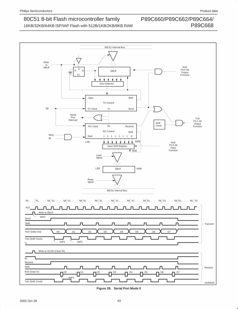
Philips Semiconductors Product data
P89C660/P89C662/P89C664/P89C668
80C51 8-bit Flash microcontroller family16KB/32KB/64KB ISP/IAP Flash with 512B/1KB/2KB/8KB RAM
2002 Oct 28 43
80C51 Internal Bus
SBUF
Zero Detector
D QS
CL
Write to
SBUF
TX Control
TX Clock Send
ShiftStart
S6
RX Control
Start
Shift
ReceiveRX Clock
T1
R1
SerialPort
Interrupt
1 1 1 1 1 1 1 0
Input Shift Register
REN
RI
LoadSBUF
Shift
ShiftClock
RxDP3.0 AltOutput
Function
TxDP3.1 AltOutput
Function
SBUF
ReadSBUF
80C51 Internal Bus
RxDP3.0 Alt
InputFunction
Write to SBUF
S6P2Send
Shift
RxD (Data Out) D0 D1 D2 D3 D4 D5 D6 D7
Transmit
TxD (Shift Clock)
TIS3P1 S6P1
Write to SCON (Clear RI)
RI
Receive
Shift
RxD (Data In) D0 D1 D2 D3 D4 D5 D6
TxD (Shift Clock)
S5P2
Receive
D7
ALE
S4 . . S1 S6. . . . S1 S6. . . . S1 S6. . . . S1 S6. . . . S1 S6. . . . S1 S6. . . . S1 S6. . . . S1 S6. . . . S1 S6. . . . S1 S6. . . . S1
SU00539
LSB
LSB MSB
MSB
Figure 28. Serial Port Mode 0

Philips Semiconductors Product data
P89C660/P89C662/P89C664/P89C668
80C51 8-bit Flash microcontroller family16KB/32KB/64KB ISP/IAP Flash with 512B/1KB/2KB/8KB RAM
2002 Oct 28 44
80C51 Internal Bus
SBUF
Zero Detector
D QS
CL
Write to
SBUF
TX Control
TX Clock Send
DataStart
RX ControlStart
RX Clock RI
T1
SerialPort
Interrupt
Input Shift Register(9 Bits)
LoadSBUF
Shift
SBUF
ReadSBUF
80C51 Internal Bus
TxD
TB8
÷ 16
1-to-0TransitionDetector
Sample
÷ 2
Timer 1Overflow
SMOD = 1SMOD = 0
Shift
Bit Detector
Transmit
Send
S1P1
Shift
TXClock
Write to SBUF
Start BitTxD Stop BitD0 D1 D2 D3 D4 D5 D6 D7
TI
RxD
RXClock
÷ 16 Reset
StartBitRxD Stop BitD0 D1 D2 D3 D4 D5 D6 D7
Bit DetectorSample Times
Shift
RI
Receive
Data
÷ 16
LoadSBUF
Shift
1FFH
SU00540
Figure 29. Serial Port Mode 1

Philips Semiconductors Product data
P89C660/P89C662/P89C664/P89C668
80C51 8-bit Flash microcontroller family16KB/32KB/64KB ISP/IAP Flash with 512B/1KB/2KB/8KB RAM
2002 Oct 28 45
80C51 Internal Bus
SBUF
Zero Detector
D QS
CL
Write to
SBUF
TX Control
TX Clock Send
DataStart
RX ControlStart
LoadSBUF
RX Clock
T1
SerialPort
Interrupt
Input Shift Register(9 Bits)
LoadSBUF
Shift
SBUF
ReadSBUF
80C51 Internal Bus
TxD
TB8
÷ 16
1-to-0TransitionDetector
Sample
÷ 2
SMOD = 1
SMOD = 0
Shift
Bit Detector
RxD
Stop BitGen.
Mode 2
Phase 2 Clock(1/2 fOSC)
R1
÷ 16
Shift
1FFH
Transmit
Send
S1P1
Shift
TXClock
Write to SBUF
Start BitTxD Stop BitD0 D1 D2 D3 D4 D5 D6 D7
TI
RXClock
÷ 16 Reset
StartBitRxD Stop BitD0 D1 D2 D3 D4 D5 D6 D7
Bit DetectorSample Times
Shift
RI
Receive
Data
(SMOD isPCON.7)
TB8
RB8
Stop Bit Gen.
SU00541
Figure 30. Serial Port Mode 2

Philips Semiconductors Product data
P89C660/P89C662/P89C664/P89C668
80C51 8-bit Flash microcontroller family16KB/32KB/64KB ISP/IAP Flash with 512B/1KB/2KB/8KB RAM
2002 Oct 28 46
80C51 Internal Bus
SBUF
Zero Detector
D QS
CL
Write to
SBUF
TX Control
TX Clock Send
DataStart
RX ControlStart
RX Clock
T1
SerialPort
Interrupt
Input Shift Register(9 Bits)
LoadSBUF
Shift
SBUF
ReadSBUF
80C51 Internal Bus
TxD
TB8
÷ 16
1-to-0TransitionDetector
Sample
÷ 2
Timer 1Overflow
SMOD = 1SMOD = 0
Shift
Bit Detector
RxD
R1
÷ 16
LoadSBUF
Shift
1FFH
Transmit
Send
S1P1
Shift
TXClock
Write to SBUF
Start BitTxD Stop BitD0 D1 D2 D3 D4 D5 D6 D7
TI
RXClock
÷ 16 Reset
StartBitRxD Stop BitD0 D1 D2 D3 D4 D5 D6 D7
Bit DetectorSample Times
Shift
RI
Receive
Data
TB8
RB8
Stop Bit Gen.
SU00542
Figure 31. Serial Port Mode 3

Philips Semiconductors Product data
P89C660/P89C662/P89C664/P89C668
80C51 8-bit Flash microcontroller family16KB/32KB/64KB ISP/IAP Flash with 512B/1KB/2KB/8KB RAM
2002 Oct 28 47
Enhanced UARTIn addition to the standard operation, the UART can perform framingerror detect by looking for missing stop bits, and automatic addressrecognition. The UART also fully supports multiprocessorcommunication as does the standard 80C51 UART.
When used for framing error detect, the UART looks for missing stopbits in the communication. A missing bit will set the FE bit in theS0CON register. The FE bit shares the S0CON.7 bit with SM0, andthe function of S0CON.7 is determined by PCON.6 (SMOD0) (seeFigure 32). If SMOD0 is set then S0CON.7 functions as FE.S0CON.7 functions as SM0 when SMOD0 is cleared. When used asFE, S0CON.7 can only be cleared by software (refer to Figure 33).
Automatic Address RecognitionAutomatic Address Recognition is a feature which allows the UARTto recognize certain addresses in the serial bit stream by usinghardware to make the comparisons. This feature saves a great dealof software overhead by eliminating the need for the software toexamine every serial address which passes by the serial port. Thisfeature is enabled by setting the SM2 bit in S0CON. In the 9-bitUART modes (mode 2 and mode 3), the Receive Interrupt flag (RI)will be automatically set when the received byte contains either the“Given” address or the “Broadcast” address. The 9-bit moderequires that the 9th information bit is a 1 to indicate that thereceived information is an address and not data. Automatic addressrecognition is shown in Figure 34.
The 8-bit mode is called Mode 1. In this mode, the RI flag will be setif SM2 is enabled and the information received has a valid stop bitfollowing the 8 address bits, and the information is either a Given orBroadcast address.
Mode 0 is the Shift Register mode and SM2 is ignored.
Using the Automatic Address Recognition feature allows a master toselectively communicate with one or more slaves by invoking theGiven slave address or addresses. All of the slaves may becontacted by using the Broadcast address. Two special FunctionRegisters are used to define the slave’s address, SADDR, and theaddress mask, SADEN. SADEN is used to define which bits in theSADDR are to be used and which bits are “don’t care”. The SADENmask can be logically ANDed with the SADDR to create the “Given”address which the master will use for addressing each of the slaves.Use of the Given address allows multiple slaves to be recognizedwhile excluding others. The following examples will help to show theversatility of this scheme:
Slave 0 SADDR = 1100 0000SADEN = 1111 1101Given = 1100 00X0
Slave 1 SADDR = 1100 0000SADEN = 1111 1110Given = 1100 000X
In the above example SADDR is the same and the SADEN data isused to differentiate between the two slaves. Slave 0 requires a 0 inbit 0 and it ignores bit 1. Slave 1 requires a 0 in bit 1 and bit 0 isignored. A unique address for Slave 0 would be 1100 0010 sinceslave 1 requires a 0 in bit 1. A unique address for slave 1 would be1100 0001 since a 1 in bit 0 will exclude slave 0. Both slaves can beselected at the same time by an address which has bit 0 = 0 (forslave 0) and bit 1 = 0 (for slave 1). Thus, both could be addressedwith 1100 0000.
In a more complex system the following could be used to selectslaves 1 and 2 while excluding slave 0:
Slave 0 SADDR = 1100 0000SADEN = 1111 1001Given = 1100 0XX0
Slave 1 SADDR = 1110 0000SADEN = 1111 1010Given = 1110 0X0X
Slave 2 SADDR = 1110 0000SADEN = 1111 1100Given = 1110 00XX
In the above example the differentiation among the 3 slaves is in thelower 3 address bits. Slave 0 requires that bit 0 = 0 and it can beuniquely addressed by 1110 0110. Slave 1 requires that bit 1 = 0 andit can be uniquely addressed by 1110 and 0101. Slave 2 requiresthat bit 2 = 0 and its unique address is 1110 0011. To select Slaves 0and 1 and exclude Slave 2 use address 1110 0100, since it isnecessary to make bit 2 = 1 to exclude slave 2.
The Broadcast Address for each slave is created by taking thelogical OR of SADDR and SADEN. Zeros in this result are trendedas don’t-cares. In most cases, interpreting the don’t-cares as ones,the broadcast address will be FF hexadecimal.
Upon reset, SADDR (SFR address 0A9H) and SADEN (SFRaddress 0B9H) are leaded with 0s. This produces a given addressof all “don’t cares” as well as a Broadcast address of all “don’tcares”. This effectively disables the Automatic Addressing mode andallows the microcontroller to use standard 80C51 type UART driverswhich do not make use of this feature.

Philips Semiconductors Product data
P89C660/P89C662/P89C664/P89C668
80C51 8-bit Flash microcontroller family16KB/32KB/64KB ISP/IAP Flash with 512B/1KB/2KB/8KB RAM
2002 Oct 28 48
S0CON Address = 98H Reset Value = 0000 0000B
SM0/FE SM1 SM2 REN TB8 RB8 Tl Rl
Bit Addressable
(SMOD0 = 0/1)*
Symbol Function
FE Framing Error bit. This bit is set by the receiver when an invalid stop bit is detected. The FE bit is not cleared by validframes but should be cleared by software. The SMOD0 bit must be set to enable access to the FE bit.
SM0 Serial Port Mode Bit 0, (SMOD0 must = 0 to access bit SM0)
SM1 Serial Port Mode Bit 1SM0 SM1 Mode Description Baud Rate**
0 0 0 shift register fOSC/6 (6 clock mode) or fOSC/12 (12 clock mode)0 1 1 8-bit UART variable1 0 2 9-bit UART fOSC/32 or fOSC/16 (6 clock mode) or
fOSC/64 or fOSC/32 (12 clock mode)1 1 3 9-bit UART variable
SM2 Enables the Automatic Address Recognition feature in Modes 2 or 3. If SM2 = 1 then Rl will not be set unless thereceived 9th data bit (RB8) is 1, indicating an address, and the received byte is a Given or Broadcast Address.In Mode 1, if SM2 = 1 then Rl will not be activated unless a valid stop bit was received, and the received byte is aGiven or Broadcast Address. In Mode 0, SM2 should be 0.
REN Enables serial reception. Set by software to enable reception. Clear by software to disable reception.
TB8 The 9th data bit that will be transmitted in Modes 2 and 3. Set or clear by software as desired.
RB8 In modes 2 and 3, the 9th data bit that was received. In Mode 1, if SM2 = 0, RB8 is the stop bit that was received. In Mode 0, RB8 is not used.
Tl Transmit interrupt flag. Set by hardware at the end of the 8th bit time in Mode 0, or at the beginning of the stop bit in theother modes, in any serial transmission. Must be cleared by software.
Rl Receive interrupt flag. Set by hardware at the end of the 8th bit time in Mode 0, or halfway through the stop bit time inthe other modes, in any serial reception (except see SM2). Must be cleared by software.
NOTE:*SMOD0 is located at PCON6.**fOSC = oscillator frequency SU01451
Bit: 7 6 5 4 3 2 1 0
Figure 32. S0CON: Serial Port Control Register

Philips Semiconductors Product data
P89C660/P89C662/P89C664/P89C668
80C51 8-bit Flash microcontroller family16KB/32KB/64KB ISP/IAP Flash with 512B/1KB/2KB/8KB RAM
2002 Oct 28 49
SMOD1 SMOD0 – POF LVF GF0 GF1 IDLPCON(87H)
SM0 / FE SM1 SM2 REN TB8 RB8 TI RI S0CON(98H)
D0 D1 D2 D3 D4 D5 D6 D7 D8
STOP BIT
DATA BYTE ONLY IN MODE 2, 3
START BIT
SET FE BIT IF STOP BIT IS 0 (FRAMING ERROR)
SM0 TO UART MODE CONTROL
0 : S0CON.7 = SM01 : S0CON.7 = FE
SU01452
Figure 33. UART Framing Error Detection
SM0 SM1 SM2 REN TB8 RB8 TI RI S0CON(98H)
D0 D1 D2 D3 D4 D5 D6 D7 D8
11
10
COMPARATOR
1 1 X
RECEIVED ADDRESS D0 TO D7
PROGRAMMED ADDRESS
IN UART MODE 2 OR MODE 3 AND SM2 = 1: INTERRUPT IF REN=1, RB8=1 AND “RECEIVED ADDRESS” = “PROGRAMMED ADDRESS”– WHEN OWN ADDRESS RECEIVED, CLEAR SM2 TO RECEIVE DATA BYTES– WHEN ALL DATA BYTES HAVE BEEN RECEIVED: SET SM2 TO WAIT FOR NEXT ADDRESS.
SU01453
Figure 34. UART Multiprocessor Communication, Automatic Address Recognition

Philips Semiconductors Product data
P89C660/P89C662/P89C664/P89C668
80C51 8-bit Flash microcontroller family16KB/32KB/64KB ISP/IAP Flash with 512B/1KB/2KB/8KB RAM
2002 Oct 28 50
Interrupt Priority StructureThe P89C660/662/664/668 has an 8 source four-level interruptstructure (see Table 13).
There are 4 SFRs associated with the four-level interrupt. They arethe IE, IP, IEN1, and IPH (see Figures 35, 36, 37, and 38). The IPH(Interrupt Priority High) register makes the four-level interruptstructure possible. The IPH is located at SFR address B7H. Thestructure of the IPH register and a description of its bits is shown inFigure 37.
The function of the IPH SFR, when combined with the IP SFR,determines the priority of each interrupt. The priority of eachinterrupt is determined as shown in the following table:
PRIORITY BITSINTERRUPT PRIORITY LEVEL
IPH.x IP.xINTERRUPT PRIORITY LEVEL
0 0 Level 0 (lowest priority)
0 1 Level 1
1 0 Level 2
1 1 Level 3 (highest priority)
The priority scheme for servicing the interrupts is the same as thatfor the 80C51, except that there are four interrupt levels rather thantwo (as on the 80C51). An interrupt will be serviced as long as aninterrupt of equal or higher priority is not already being serviced. Ifan interrupt of equal or higher level priority is being serviced, thenew interrupt will wait until it is finished before being serviced. If alower priority level interrupt is being serviced, it will be stopped andthe new interrupt serviced. When the new interrupt is finished, thelower priority level interrupt that was stopped will be completed.
Table 13. Interrupt TableSOURCE POLLING PRIORITY REQUEST BITS HARDWARE CLEAR? VECTOR ADDRESS
X0 1 IE0 N (L)1 Y (T)2 03H
SI01 (I2C) 2 — N 2BH
T0 3 TP0 Y 0BH
X1 4 IE1 N (L) Y (T) 13H
T1 5 TF1 Y 1BH
SP 6 RI, TI N 23H
T2 7 TF2, EXF2 N 3BH
PCA 8 CF, CCFnn = 0–4
N 33H
NOTES:1. L = Level activated2. T = Transition activated
EX0IEN0 (0A8H)
Enable Bit = 1 enables the interrupt.Enable Bit = 0 disables it.
BIT SYMBOL FUNCTIONIEN0.7 EA Global disable bit. If EA = 0, all interrupts are disabled. If EA = 1, each interrupt can be individually
enabled or disabled by setting or clearing its enable bit.IEN0.6 EC PCA interrupt enable bitIEN0.5 ES1 I2C interrupt enable bit.IEN0.4 ES0 Serial Port interrupt enable bit.IEN0.3 ET1 Timer 1 interrupt enable bit.IEN0.2 EX1 External interrupt 1 enable bit.IEN0.1 ET0 Timer 0 interrupt enable bit.IEN0.0 EX0 External interrupt 0 enable bit.
SU01454
ET0EX1ET1ES0ES1ECEA
01234567
Figure 35. IE Registers

Philips Semiconductors Product data
P89C660/P89C662/P89C664/P89C668
80C51 8-bit Flash microcontroller family16KB/32KB/64KB ISP/IAP Flash with 512B/1KB/2KB/8KB RAM
2002 Oct 28 51
PX0IP (0B8H)
Priority Bit = 1 assigns high priorityPriority Bit = 0 assigns low priority
BIT SYMBOL FUNCTIONIP.7 PT2 Timer 2 interrupt priority bit.IP.6 PPC PCA interrupt priority bitIP.5 PS1 Serial I/O1 (I2C) interrupt priority bit.IP.4 PS0 Serial Port interrupt priority bit.IP.3 PT1 Timer 1 interrupt priority bit.IP.2 PX1 External interrupt 1 priority bit.IP.1 PT0 Timer 0 interrupt priority bit.IP.0 PX0 External interrupt 0 priority bit.
SU01455
PT0PX1PT1PS0PS1PPCPT2
01234567
Figure 36. IP Registers
PX0HIPH (B7H)
Priority Bit = 1 assigns higher priorityPriority Bit = 0 assigns lower priority
BIT SYMBOL FUNCTIONIPH.7 PT2H Timer 2 interrupt priority bit high.IPH.6 PPCH PCA interrupt priority bitIPH.5 PS1H Serial I/O (I2C) interrupt priority bit high.IPH.4 PS0H Serial Port interrupt priority bit high.IPH.3 PT1H Timer 1 interrupt priority bit high.IPH.2 PX1H External interrupt 1 priority bit high.IPH.1 PT0H Timer 0 interrupt priority bit high.IPH.0 PX0H External interrupt 0 priority bit high.
SU01456
PT0HPX1HPT1HPS0HPS1HPPCHPT2H
01234567
Figure 37. IPH Registers
ET2IEN1 (E8H)
Enable Bit = 1 enables the interruptEnable Bit = 0 disables the interrupt
BIT SYMBOL FUNCTIONIEN1.7 —IEN1.6 —IEN1.5 —IEN1.4 —IEN1.3 —IEN1.2 —IEN1.1 —IEN1.0 ET2 Timer 2 interrupt enable bit.
SU01095
———————
01234567
Figure 38. IEN1 Registers

Philips Semiconductors Product data
P89C660/P89C662/P89C664/P89C668
80C51 8-bit Flash microcontroller family16KB/32KB/64KB ISP/IAP Flash with 512B/1KB/2KB/8KB RAM
2002 Oct 28 52
Reduced EMI ModeThe AO bit (AUXR.0) in the AUXR register when set disables theALE output.
Reduced EMI Mode
AUXR (8EH)
7 6 5 4 3 2 1 0
– – – – – – EXTRAM AO
AUXR.1 EXTRAM (See more detailed description inAUXR.0 AO Figure 53.)
Dual DPTRThe dual DPTR structure (see Figure 39) is a way by which the chipwill specify the address of an external data memory location. Thereare two 16-bit DPTR registers that address the external memory,and a single bit called DPS (AUXR1.0), that allows the programcode to switch between them.
• New Register Name: AUXR1#
• SFR Address: A2H
• Reset Value: xxxxx0x0B
AUXR1 (A2H)
7 6 5 4 3 2 1 0
– – ENBOOT – GF2 0 – DPS
Where:DPS (AUXR1.0), enables switching between DPTR0 and DPTR1.
Select Reg DPS
DPTR0 0
DPTR1 1
The DPS bit status should be saved by software when switchingbetween DPTR0 and DPTR1.
The GF2 bit is a general purpose user-defined flag. Note that bit 2 isnot writable and is always read as a zero. This allows the DPS bit tobe quickly toggled simply by executing an INC AUXR1 instructionwithout affecting the GF2 bit.
The ENBOOT bit determines whether the BOOTROM is enabledor disabled. This bit will automatically be set if the status byte isnon zero during reset or PSEN is pulled low, ALE floats high, andEA > VIH on the falling edge of reset. Otherwise, this bit will becleared during reset.
DPS
DPTR1
DPTR0
DPH(83H)
DPL(82H) EXTERNAL
DATAMEMORY
SU00745A
BIT0AUXR1
Figure 39.
DPTR InstructionsThe instructions, that refer to DPTR, refer to the data pointer that iscurrently selected by the DPS bit (AUXR1.0). The six instructionsthat use the DPTR are as follows:
INC DPTR Increments the data pointer by 1
MOV DPTR, #data16 Loads the DPTR with a 16-bit constant
MOV A, @ A+DPTR Move code byte relative to DPTR to ACC
MOVX A, @ DPTR Move external RAM (16-bit address) toACC
MOVX @ DPTR , A Move ACC to external RAM (16-bitaddress)
JMP @ A + DPTR Jump indirect relative to DPTR
The data pointer can be accessed on a byte-by-byte basis byspecifying the low or high byte in an instruction which accesses theSFRs. See application note AN458 for more details.

Philips Semiconductors Product data
P89C660/P89C662/P89C664/P89C668
80C51 8-bit Flash microcontroller family16KB/32KB/64KB ISP/IAP Flash with 512B/1KB/2KB/8KB RAM
2002 Oct 28 53
Programmable Counter Array (PCA)The Programmable Counter Array available on the 89C66x is aspecial 16-bit Timer that has five 16-bit capture/compare modulesassociated with it. Each of the modules can be programmed tooperate in one of four modes: rising and/or falling edge capture,software timer, high-speed output, or pulse width modulator. Eachmodule has a pin associated with it in port 1. Module 0 is connectedto P1.3(CEX0), module 1 to P1.4(CEX1), etc. The basic PCAconfiguration is shown in Figure 40.
The PCA timer is a common time base for all five modules and canbe programmed to run at: 1/6 the oscillator frequency, 1/2 theoscillator frequency, the Timer 0 overflow, or the input on the ECI pin(P1.2). The timer count source is determined from the CPS1 andCPS0 bits in the CMOD SFR as follows (see Figure 43):
CPS1 CPS0 PCA Timer Count Source0 0 1/6 oscillator frequency (6 clock mode);
1/12 oscillator frequency (12 clock mode)0 1 1/2 oscillator frequency (6 clock mode);
1/4 oscillator frequency (12 clock mode)1 0 Timer 0 overflow1 1 External Input at ECI pin
In the CMOD SFR, there are three additional bits associated withthe PCA. They are CIDL which allows the PCA to stop during idlemode, WDTE which enables or disables the watchdog function onmodule 4, and ECF which, when set, causes an interrupt and thePCA overflow flag CF (in the CCON SFR) to be set when the PCAtimer overflows. These functions are shown in Figure 41.
The watchdog timer function is implemented in module 4 (seeFigure 50).
The CCON SFR contains the run control bit for the PCA, and theflags for the PCA timer (CF) and each module (refer to Figure 44).To run the PCA the CR bit (CCON.6) must be set by software. ThePCA is shut off by clearing this bit. The CF bit (CCON.7) is set when
the PCA counter overflows and an interrupt will be generated if theECF bit in the CMOD register is set, The CF bit can only be clearedby software. Bits 0 through 4 of the CCON register are the flags forthe modules (bit 0 for module 0, bit 1 for module 1, etc.) and are setby hardware when either a match or a capture occurs. These flagsalso can only be cleared by software. The PCA interrupt system isshown in Figure 42.
Each module in the PCA has a special function register associatedwith it. These registers are: CCAPM0 for module 0, CCAPM1 formodule 1, etc. (see Figure 45). The registers contain the bits thatcontrol the mode that each module will operate in. The ECCF bit(CCAPMn.0 where n = 0, 1, 2, 3, or 4 depending on the module)enables the CCF flag in the CCON SFR to generate an interruptwhen a match or compare occurs in the associated module. PWM(CCAPMn.1) enables the pulse width modulation mode. The TOGbit (CCAPMn.2), when set, causes the CEX output associated withthe module to toggle when there is a match between the PCAcounter and the module’s capture/compare register. The match bitMAT (CCAPMn.3), when set, will cause the CCFn bit in the CCONregister to be set when there is a match between the PCA counterand the module’s capture/compare register.
The next two bits CAPN (CCAPMn.4) and CAPP (CCAPMn.5)determine the edge that a capture input will be active on. The CAPNbit enables the negative edge, and the CAPP bit enables the positiveedge. If both bits are set, both edges will be enabled and a capturewill occur for either transition. The last bit ECOM (CCAPMn.6), whenset, enables the comparator function. Figure 46 shows the CCAPMnsettings for the various PCA functions.
There are two additional registers associated with each of the PCAmodules. They are CCAPnH and CCAPnL and these are theregisters that store the 16-bit count when a capture occurs or acompare should occur. When a module is used in the PWM modethese registers are used to control the duty cycle of the output.
MODULE FUNCTIONS:16-BIT CAPTURE16-BIT TIMER16-BIT HIGH SPEED OUTPUT8-BIT PWMWATCHDOG TIMER (MODULE 4 ONLY)
MODULE 0
MODULE 1
MODULE 2
MODULE 3
MODULE 4
P1.3/CEX0
P1.4/CEX1
P1.5/CEX2
P3.4/CEX3
P3.5/CEX4
16 BITS
PCA TIMER/COUNTER
TIME BASE FOR PCA MODULES
16 BITS
SU01416
Figure 40. Programmable Counter Array (PCA)

Philips Semiconductors Product data
P89C660/P89C662/P89C664/P89C668
80C51 8-bit Flash microcontroller family16KB/32KB/64KB ISP/IAP Flash with 512B/1KB/2KB/8KB RAM
2002 Oct 28 54
CF CR CCF4 CCF3 CCF2 CCF1 CCF0––CCON(C0H)
CH CL
OVERFLOWINTERRUPT
16–BIT UP COUNTER
IDLE
TO PCA MODULES
CMOD(C1H)
CIDL WDTE –– –– –– CPS1 CPS0 ECF
OSC/6 (6 CLOCK MODE)OR
OSC/12 (12 CLOCK MODE)
TIMER 0 OVERFLOW
EXTERNAL INPUT(P1.2/ECI)
DECODE
00011011
SU01256
OSC/2 (6 CLOCK MODE)OR
OSC/4 (12 CLOCK MODE)
Figure 41. PCA Timer/Counter
MODULE 0
MODULE 1
MODULE 2
MODULE 3
MODULE 4
PCA TIMER/COUNTER
CF CR CCF4 CCF3 CCF2 CCF1 CCF0––
CMOD.0 ECF CCAPMn.0 ECCFn
TO INTERRUPT PRIORITY DECODER
CCON(C0H)
IE.6EC
IE.7EA
SU01097
Figure 42. PCA Interrupt System

Philips Semiconductors Product data
P89C660/P89C662/P89C664/P89C668
80C51 8-bit Flash microcontroller family16KB/32KB/64KB ISP/IAP Flash with 512B/1KB/2KB/8KB RAM
2002 Oct 28 55
CMOD Address = C1H Reset Value = 00XX X000B
CIDL WDTE – – – CPS1 CPS0 ECF
Bit:
Symbol Function
CIDL Counter Idle control: CIDL = 0 programs the PCA Counter to continue functioning during idle Mode. CIDL = 1 programsit to be gated off during idle.
WDTE Watchdog Timer Enable: WDTE = 0 disables Watchdog Timer function on PCA Module 4. WDTE = 1 enables it.
– Not implemented, reserved for future use.*
CPS1 PCA Count Pulse Select bit 1.
CPS0 PCA Count Pulse Select bit 0.CPS1 CPS0 Selected PCA Input**
0 0 0 Internal clock, fOSC/6 in 6 clock mode (fOSC/12 in 12 clock mode)0 1 1 Internal clock, fOSC/2 in 6 clock mode (fOSC/4 in 12 clock mode)1 0 2 Timer 0 overflow1 1 3 External clock at ECI/P1.2 pin
(max. rate = fOSC/4 in 6 clock mode, fOCS/8 in 12 clock mode)
ECF PCA Enable Counter Overflow interrupt: ECF = 1 enables CF bit in CCON to generate an interrupt. ECF = 0 disablesthat function of CF.
NOTE:* User software should not write 1s to reserved bits. These bits may be used in future 8051 family products to invoke new features. In that case, the reset or inactive value of the
new bit will be 0, and its active value will be 1. The value read from a reserved bit is indeterminate.** fOSC = oscillator frequency
SU01257
7 6 5 4 3 2 1 0
Figure 43. CMOD: PCA Counter Mode Register
CCON Address = 0C0H Reset Value = 00X0 0000B
CF CR – CCF4 CCF3 CCF2 CCF1 CCF0
Bit Addressable
Bit:
Symbol Function
CF PCA Counter Overflow flag. Set by hardware when the counter rolls over. CF flags an interrupt if bit ECF in CMOD isset. CF may be set by either hardware or software but can only be cleared by software.
CR PCA Counter Run control bit. Set by software to turn the PCA counter on. Must be cleared by software to turn the PCAcounter off.
– Not implemented, reserved for future use*.
CCF4 PCA Module 4 interrupt flag. Set by hardware when a match or capture occurs. Must be cleared by software.
CCF3 PCA Module 3 interrupt flag. Set by hardware when a match or capture occurs. Must be cleared by software.
CCF2 PCA Module 2 interrupt flag. Set by hardware when a match or capture occurs. Must be cleared by software.
CCF1 PCA Module 1 interrupt flag. Set by hardware when a match or capture occurs. Must be cleared by software.
CCF0 PCA Module 0 interrupt flag. Set by hardware when a match or capture occurs. Must be cleared by software.
NOTE:* User software should not write 1s to reserved bits. These bits may be used in future 8051 family products to invoke new features. In that case, the reset or inactive value of the
new bit will be 0, and its active value will be 1. The value read from a reserved bit is indeterminate.
SU01099
7 6 5 4 3 2 1 0
Figure 44. CCON: PCA Counter Control Register

Philips Semiconductors Product data
P89C660/P89C662/P89C664/P89C668
80C51 8-bit Flash microcontroller family16KB/32KB/64KB ISP/IAP Flash with 512B/1KB/2KB/8KB RAM
2002 Oct 28 56
CCAPMn Address CCAPM0 0C2HCCAPM1 0C3HCCAPM2 0C4H CCAPM3 0C5H CCAPM4 0C6H
Reset Value = X000 0000B
– ECOMn CAPPn CAPNn MATn TOGn PWMn ECCFn
Not Bit Addressable
Bit:
Symbol Function
– Not implemented, reserved for future use*.ECOMn Enable Comparator. ECOMn = 1 enables the comparator function.CAPPn Capture Positive, CAPPn = 1 enables positive edge capture.CAPNn Capture Negative, CAPNn = 1 enables negative edge capture.MATn Match. When MATn = 1, a match of the PCA counter with this module’s compare/capture register causes the CCFn bit
in CCON to be set, flagging an interrupt.TOGn Toggle. When TOGn = 1, a match of the PCA counter with this module’s compare/capture register causes the CEXn
pin to toggle.PWMn Pulse Width Modulation Mode. PWMn = 1 enables the CEXn pin to be used as a pulse width modulated output.ECCFn Enable CCF interrupt. Enables compare/capture flag CCFn in the CCON register to generate an interrupt.
NOTE:*User software should not write 1s to reserved bits. These bits may be used in future 8051 family products to invoke new features. In that case, the reset or inactive value of the newbit will be 0, and its active value will be 1. The value read from a reserved bit is indeterminate.
SU01100
7 6 5 4 3 2 1 0
Figure 45. CCAPMn: PCA Modules Compare/Capture Registers
– ECOMn CAPPn CAPNn MATn TOGn PWMn ECCFn MODULE FUNCTION
X 0 0 0 0 0 0 0 No operation
X X 1 0 0 0 0 X 16-bit capture by a positive-edge trigger on CEXn
X X 0 1 0 0 0 X 16-bit capture by a negative trigger on CEXn
X X 1 1 0 0 0 X 16-bit capture by a transition on CEXn
X 1 0 0 1 0 0 X 16-bit Software Timer
X 1 0 0 1 1 0 X 16-bit High Speed Output
X 1 0 0 0 0 1 0 8-bit PWM
X 1 0 0 1 X 0 X Watchdog Timer
Figure 46. PCA Module Modes (CCAPMn Register)
PCA Capture ModeTo use one of the PCA modules in the capture mode, either one orboth of the CCAPM bits CAPN and CAPP for that module must beset. The external CEX input for the module (on port 1) is sampled fora transition. When a valid transition occurs, the PCA hardware loadsthe value of the PCA counter registers (CH and CL) into themodule’s capture registers (CCAPnL and CCAPnH). If the CCFn bitfor the module in the CCON SFR and the ECCFn bit in the CCAPMnSFR are set, then an interrupt will be generated (refer to Figure 47).
16-bit Software Timer ModeThe PCA modules can be used as software timers by setting boththe ECOM and MAT bits in the modules CCAPMn register. The PCAtimer will be compared to the module’s capture registers, and whena match occurs, an interrupt will occur if the CCFn (CCON SFR) andthe ECCFn (CCAPMn SFR) bits for the module are both set (seeFigure 48).
High Speed Output ModeIn this mode, the CEX output (on port 1) associated with the PCAmodule will toggle each time a match occurs between the PCA
counter and the module’s capture registers. To activate this mode,the TOG, MAT, and ECOM bits in the module’s CCAPMn SFR mustbe set (see Figure 49).
Pulse Width Modulator ModeAll of the PCA modules can be used as PWM outputs. Figure 50shows the PWM function. The frequency of the output depends onthe source for the PCA timer. All of the modules will have the samefrequency of output because they all share the PCA timer. The dutycycle of each module is independently variable by using themodule’s capture register CCAPLn. When the value of the PCA CLSFR is less than the value in the module’s CCAPLn SFR, the outputwill be low. When it is equal to or greater than, the output will behigh. When CL overflows from FF to 00, CCAPLn is reloaded withthe value in CCAPHn. This allows PWM update without glitches.The PWM and ECOM bits in the module’s CCAPMn register mustbe set to enable the PWM mode.

Philips Semiconductors Product data
P89C660/P89C662/P89C664/P89C668
80C51 8-bit Flash microcontroller family16KB/32KB/64KB ISP/IAP Flash with 512B/1KB/2KB/8KB RAM
2002 Oct 28 57
CF CR CCF4 CCF3 CCF2 CCF1 CCF0––CCON (0C0H)
–– ECOMn CAPPn CAPNn MATn TOGn PWMn ECCFn CCAPMn, n= 0 to 4(C2H – C6H)
CH CL
CCAPnH CCAPnL
CEXnCAPTURE
PCA INTERRUPT
PCA TIMER/COUNTER
0 0 0 0
(TO CCFn)
SU01101
Figure 47. PCA Capture Mode
MATCH
CF CR CCF4 CCF3 CCF2 CCF1 CCF0––CCON(C0H)
–– ECOMn CAPPn CAPNn MATn TOGn PWMn ECCFn CCAPMn, n= 0 to 4(C2H – C6H)
CH CL
CCAPnH CCAPnLPCA INTERRUPT
PCA TIMER/COUNTER
0 00 0
16–BIT COMPARATOR
(TO CCFn)
ENABLE
WRITE TO CCAPnH RESET
WRITE TO CCAPnL
0 1
SU01102
Figure 48. PCA Compare Mode

Philips Semiconductors Product data
P89C660/P89C662/P89C664/P89C668
80C51 8-bit Flash microcontroller family16KB/32KB/64KB ISP/IAP Flash with 512B/1KB/2KB/8KB RAM
2002 Oct 28 58
CF CR CCF4 CCF3 CCF2 CCF1 CCF0––CCON(C0H)
–– ECOMn CAPPn CAPNn MATn TOGn PWMn ECCFn CCAPMn, n: 0..4(C2H – C6H)
CH CL
CCAPnH CCAPnLPCA INTERRUPT
PCA TIMER/COUNTER
1 00 0
16–BIT COMPARATOR
(TO CCFn)
WRITE TO CCAPnH RESET
WRITE TO CCAPnL
0 1
ENABLE
CEXn
TOGGLE
MATCH
SU01103
Figure 49. PCA High Speed Output Mode
CL < CCAPnL
–– ECOMn CAPPn CAPNn MATn TOGn PWMn ECCFn CCAPMn, n: 0..4(C2H – C6H)
PCA TIMER/COUNTER
0 00 0
CL
CCAPnL
CEXn8–BIT
COMPARATOR
OVERFLOW
CCAPnH
ENABLE
0
1
CL >= CCAPnL
0
SU01104
Figure 50. PCA PWM Mode

Philips Semiconductors Product data
P89C660/P89C662/P89C664/P89C668
80C51 8-bit Flash microcontroller family16KB/32KB/64KB ISP/IAP Flash with 512B/1KB/2KB/8KB RAM
2002 Oct 28 59
–– ECOMn CAPPn CAPNn MATn TOGn PWMn ECCFn CCAPM4(C6H)
CH CL
CCAP4H CCAP4L
RESET
PCA TIMER/COUNTER
X 00 0
16–BIT COMPARATORMATCHENABLE
WRITE TO CCAP4L RESET
WRITE TO CCAP4H
1 0
1
CMOD(C1H)
CIDL WDTE –– –– –– CPS1 CPS0 ECF
X
SU01105
MODULE 4
Figure 51. PCA Watchdog Timer m(Module 4 only)
PCA Watchdog TimerAn on-board watchdog timer is available with the PCA to improve thereliability of the system without increasing chip count. Watchdogtimers are useful for systems that are susceptible to noise, powerglitches, or electrostatic discharge. Module 4 is the only PCA modulethat can be programmed as a watchdog. However, this module canstill be used for other modes if the watchdog is not needed.
Figure 51 shows a diagram of how the watchdog works. The userpre-loads a 16-bit value in the compare registers. Just like the othercompare modes, this 16-bit value is compared to the PCA timervalue. If a match is allowed to occur, an internal reset will begenerated. This will not cause the RST pin to be driven high.
In order to hold off the reset, the user has three options:1. periodically change the compare value so it will never match the
PCA timer,
2. periodically change the PCA timer value so it will never matchthe compare values, or
3. disable the watchdog by clearing the WDTE bit before a matchoccurs and then re-enable it.
The first two options are more reliable because the watchdogtimer is never disabled as in option #3. If the program counter evergoes astray, a match will eventually occur and cause an internalreset. The second option is also not recommended if other PCAmodules are being used. Remember, the PCA timer is the timebase for all modules; changing the time base for other moduleswould not be a good idea. Thus, in most applications the firstsolution is the best option.
Figure 52 shows the code for initializing the watchdog timer.Module 4 can be configured in either compare mode, and the WDTEbit in CMOD must also be set. The user’s software must periodicallychange (CCAP4H,CCAP4L) to keep a match from occurring with thePCA timer (CH,CL). This code is given in the WATCHDOG routine inFigure 52.
This routine should not be part of an interrupt service routine,because if the program counter goes astray and gets stuck in aninfinite loop, interrupts will still be serviced and the watchdog willkeep getting reset. Thus, the purpose of the watchdog would bedefeated. Instead, call this subroutine from the main program within216 count of the PCA timer.

Philips Semiconductors Product data
P89C660/P89C662/P89C664/P89C668
80C51 8-bit Flash microcontroller family16KB/32KB/64KB ISP/IAP Flash with 512B/1KB/2KB/8KB RAM
2002 Oct 28 60
INIT_WATCHDOG: MOV CCAPM4, #4CH ; Module 4 in compare mode MOV CCAP4L, #0FFH ; Write to low byte first MOV CCAP4H, #0FFH ; Before PCA timer counts up to ; FFFF Hex, these compare values ; must be changed ORL CMOD, #40H ; Set the WDTE bit to enable the ; watchdog timer without changing ; the other bits in CMOD;;********************************************************************;; Main program goes here, but CALL WATCHDOG periodically.;;********************************************************************;WATCHDOG: CLR EA ; Hold off interrupts MOV CCAP4L, #00 ; Next compare value is within MOV CCAP4H, CH ; 255 counts of the current PCA SETB EA ; timer value RET
Figure 52. PCA Watchdog Timer Initialization Code

Philips Semiconductors Product data
P89C660/P89C662/P89C664/P89C668
80C51 8-bit Flash microcontroller family16KB/32KB/64KB ISP/IAP Flash with 512B/1KB/2KB/8KB RAM
2002 Oct 28 61
Expanded Data RAM AddressingThe P89C660/662/664/668 has internal data memory that ismapped into four separate segments: the lower 128 bytes of RAM,upper 128 bytes of RAM, 128 bytes Special Function Register (SFR),and 256 bytes expanded RAM (ERAM) (256 bytes for the ’660; 768bytes for the ’662; 1792 bytes for the ’664; 7936 bytes for the ’668).
The four segments are:1. The Lower 128 bytes of RAM (addresses 00H to 7FH) are
directly and indirectly addressable.
2. The Upper 128 bytes of RAM (addresses 80H to FFH) areindirectly addressable only.
3. The Special Function Registers, SFRs, (addresses 80H to FFH)are directly addressable only.
4. The 256/768/1792/7936-bytes expanded RAM (ERAM,00H – XFFH/2FFH/6FFH/1FFFH) are indirectly accessed bymove external instruction, MOVX, and with the EXTRAM bitcleared, see Figure 53.
The Lower 128 bytes can be accessed by either direct or indirectaddressing. The Upper 128 bytes can be accessed by indirectaddressing only. The Upper 128 bytes occupy the same addressspace as the SFR. That means they have the same address, but arephysically separate from SFR space.
When an instruction accesses an internal location above address7FH, the CPU knows whether the access is to the upper 128 bytesof data RAM, or to SFR space by the addressing mode used in theinstruction. Instructions that use direct addressing, access SFRspace. For example:
MOV 0A0H,A
accesses the SFR at location 0A0H (which is P2). Instructions thatuse indirect addressing, access the Upper 128 bytes of data RAM.
For example:
MOV @R0,A
where R0 contains 0A0H, accesses the data byte at address 0A0H,rather than P2 (whose address is 0A0H).
The ERAM can be accessed by indirect addressing, with EXTRAMbit cleared and MOVX instructions. This part of memory is physicallylocated on-chip, logically occupies the first 256 bytes (660), 768(662), 1792 (664), 7936 (668) of external data memory.
With EXTRAM = 0, the ERAM is indirectly addressed, using theMOVX instruction in combination with any of the registers R0, R1 ofthe selected bank or DPTR. An access to ERAM will not affect portsP0, P3.6 (WR#) and P3.7 (RD#). P2 SFR is in output state duringexternal addressing. For example, with EXTRAM = 0,
MOVX @R0,A
where R0 contains 0A0H, access the ERAM at address 0A0H ratherthan external memory. An access to external data memory locationshigher than the ERAM will be performed with the MOVX DPTRinstructions in the same way as in the standard 80C51 (with P0 andP2 as data/address bus, and P3.6 and P3.7 as write and read timingsignals. Refer to Figure 54).
With EXTRAM = 1, MOVX @Ri and MOVX @DPTR will be similarto the standard 80C51. MOVX @ Ri will provide an 8-bit addressmultiplexed with data on Port 0 and any output port pins can beused to output higher order address bits. This is to provide theexternal paging capability. MOVX @DPTR will generate a 16-bitaddress. Port 2 outputs the high-order eight address bits (thecontents of DPH) while Port 0 multiplexes the low-order eightaddress bits (the contents of DPL) with data. MOVX @Ri and MOVX@DPTR will generate either read or write signals on P3.6 (WR) andP3.7 (RD).
The stack pointer (SP) may be located anywhere in the 256 bytesRAM (lower and upper RAM) internal data memory. The stack maynot be located in the ERAM.
AUXR Reset Value = xxxx xx10B
— — — — — — EXTRAM AO
Not Bit Addressable
Bit:
Symbol Function
AO Disable/Enable ALE
AO Operating Mode0 ALE is emitted at a constant rate of 1/3 the oscillator frequency (6 clock mode; 1/6 fOSC in 12 clock mode)1 ALE is active only during off-chip memory access.
EXTRAM Internal/External RAM access using MOVX @Ri/@DPTR
EXTRAM Operating Mode0 Internal ERAM access using MOVX @Ri/@DPTR1 External data memory access.
— Not implemented, reserved for future use*.
NOTE:*User software should not write 1s to reserved bits. These bits may be used in future 8051 family products to invoke new features. In that case, the reset or inactive value of the newbit will be 0, and its active value will be 1. The value read from a reserved bit is indeterminate.
SU01711
7 6 5 4 3 2 1 0
Address = 8EH
Figure 53. AUXR: Auxiliary Register

Philips Semiconductors Product data
P89C660/P89C662/P89C664/P89C668
80C51 8-bit Flash microcontroller family16KB/32KB/64KB ISP/IAP Flash with 512B/1KB/2KB/8KB RAM
2002 Oct 28 62
ERAM256, 768,
1792 OR 7936BYTES
UPPER128 BYTES
INTERNAL RAM
LOWER128 BYTES
INTERNAL RAM
SPECIALFUNCTIONREGISTER
000
FF
00
FF
00
80 80
EXTERNALDATA
MEMORY
FFFF
0000
SU01712
FF/2FF/6FF/1FFF
Figure 54. Internal and External Data Memory Address Space with EXTRAM = 0
Hardware WatchDog Timer (One-Time Enabledwith Reset-Out for P89C660/662/664/668)The WDT is intended as a recovery method in situations where theCPU may be subjected to software upset. The WDT consists of a14-bit counter and the WatchDog Timer reset (WDTRST) SFR. TheWDT is disabled at reset. To enable the WDT, user must write 01EHand 0E1H in sequence to the WDTRST (SFR location 0A6H). WhenWDT is enabled, it will increment every machine cycle while theoscillator is running and there is no way to disable the WDT exceptthrough reset (either hardware reset or WDT overflow reset). WhenWDT overflows, it will drive an output reset HIGH pulse at the RSTpin.
Using the WDTTo enable the WDT, user must write 01EH and 0E1H in sequence tothe WDTRST (SFR location 0A6H). When WDT is enabled, the userneeds to service it by writing 01EH and 0E1H to WDTRST to avoidWDT overflow. The 14-bit counter overflows when it reaches 16383(3FFFH) and this will reset the device. When WDT is enabled, it willincrement every machine cycle while the oscillator is running. Thismeans the user must reset the WDT at least every 16383 machinecycles. To reset the WDT, the user must write 01EH and 0E1H toWDTRST. WDTRST is a write only register. The WDT countercannot be read or written. When the WDT overflows, it will generatean output RESET pulse at the RST pin. The RESET pulse durationis 98 × TOSC (6 clock mode; 196 in 12 clock mode), whereTOSC = 1/fOSC. To make the best use of the WDT, it should beserviced in those sections of code that will periodically be executedwithin the time required to prevent a WDT reset.
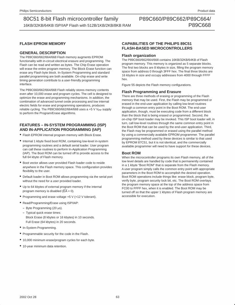
Philips Semiconductors Product data
P89C660/P89C662/P89C664/P89C668
80C51 8-bit Flash microcontroller family16KB/32KB/64KB ISP/IAP Flash with 512B/1KB/2KB/8KB RAM
2002 Oct 28 63
FLASH EPROM MEMORY
GENERAL DESCRIPTIONThe P89C660/662/664/668 Flash memory augments EPROMfunctionality with in-circuit electrical erasure and programming. TheFlash can be read and written as bytes. The Chip Erase operationwill erase the entire program memory. The Block Erase function canerase any Flash byte block. In-System Programming and standardparallel programming are both available. On-chip erase and writetiming generation contribute to a user-friendly programminginterface.
The P89C660/662/664/668 Flash reliably stores memory contentseven after 10,000 erase and program cycles. The cell is designed tooptimize the erase and programming mechanisms. In addition, thecombination of advanced tunnel oxide processing and low internalelectric fields for erase and programming operations, producesreliable cycling. The P89C660/662/664/668 uses a +5 V VPP supplyto perform the Program/Erase algorithms.
FEATURES – IN-SYSTEM PROGRAMMING (ISP)AND IN-APPLICATION PROGRAMMING (IAP)• Flash EPROM internal program memory with Block Erase.
• Internal 1 kbyte fixed boot ROM, containing low-level in-systemprogramming routines and a default serial loader. User programcan call these routines to perform In-Application Programming(IAP). The Boot ROM can be turned off to provide access to thefull 64 kbyte of Flash memory.
• Boot vector allows user provided Flash loader code to resideanywhere in the Flash memory space. This configuration providesflexibility to the user.
• Default loader in Boot ROM allows programming via the serial portwithout the need for a user provided loader.
• Up to 64 kbytes of external program memory if the internalprogram memory is disabled (EA = 0).
• Programming and erase voltage +5 V (+12 V tolerant).
• Read/Programming/Erase using ISP/IAP:
– Byte Programming (20 s).
– Typical quick erase times:
Block Erase (8 kbytes or 16 kbytes) in 10 seconds.
Full Erase (64 kbytes) in 20 seconds.
• In-System Programming.
• Programmable security for the code in the Flash.
• 10,000 minimum erase/program cycles for each byte.
• 10-year minimum data retention.
CAPABILITIES OF THE PHILIPS 89C51FLASH-BASED MICROCONTROLLERS
Flash organizationThe P89C660/662/664/668 contains 16KB/32KB/64KB of Flashprogram memory. This memory is organized as 5 separate blocks.The first two blocks are 8 kbytes in size, filling the program memoryspace from address 0 through 3FFF hex. The final three blocks are16 kbytes in size and occupy addresses from 4000 through FFFFhex.
Figure 55 depicts the Flash memory configurations.
Flash Programming and ErasureThere are three methods of erasing or programming of the Flashmemory that may be used. First, the Flash may be programmed orerased in the end-user application by calling low-level routinesthrough a common entry point in the Boot ROM. The end-userapplication, though, must be executing code from a different blockthan the block that is being erased or programmed. Second, theon-chip ISP boot loader may be invoked. This ISP boot loader will, inturn, call low-level routines through the same common entry point inthe Boot ROM that can be used by the end-user application. Third,the Flash may be programmed or erased using the parallel methodby using a commercially available EPROM programmer. The parallelprogramming method used by these devices is similar to that usedby EPROM 87C51, but it is not identical, and the commerciallyavailable programmer will need to have support for these devices.
Boot ROMWhen the microcontroller programs its own Flash memory, all of thelow level details are handled by code that is permanently containedin a 1 kbyte “Boot ROM” that is separate from the Flash memory.A user program simply calls the common entry point with appropriateparameters in the Boot ROM to accomplish the desired operation.Boot ROM operations include things like: erase block, program byte,verify byte, program security lock bit, etc. The Boot ROM overlaysthe program memory space at the top of the address space fromFC00 to FFFF hex, when it is enabled. The Boot ROM may beturned off so that the upper 1 kbytes of Flash program memory areaccessible for execution.

Philips Semiconductors Product data
P89C660/P89C662/P89C664/P89C668
80C51 8-bit Flash microcontroller family16KB/32KB/64KB ISP/IAP Flash with 512B/1KB/2KB/8KB RAM
2002 Oct 28 64
FFFF
C000
8000
4000
2000
0000
BLOCK 4
16 KBYTES
BLOCK 3
16 KBYTES
BLOCK 2
16 KBYTES
BLOCK 1
8 KBYTES
BLOCK 0
8 KBYTES
PROGRAMADDRESS
BOOT ROM
(1 KBYTE)
FFFF
FC00
SU01264
89C664/89C668
89C662
89C660
Figure 55. Flash Memory Configurations
Power-On Reset Code ExecutionThe P89C660/662/664/668 contains two special Flash registers: theBOOT VECTOR and the STATUS BYTE. At the falling edge of reset,the P89C660/662/664/668 examines the contents of the StatusByte. If the Status Byte is set to zero, power-up execution starts atlocation 0000H, which is the normal start address of the user’sapplication code. When the Status Byte is set to a value other thanzero, the contents of the Boot Vector is used as the high byte of theexecution address and the low byte is set to 00H. The factorydefault setting is 0FCH, corresponds to the address 0FC00H for thefactory masked-ROM ISP boot loader. A custom boot loader can bewritten with the Boot Vector set to the custom boot loader.
NOTE: When erasing the Status Byte or Boot Vector,both bytes are erased at the same time. It is necessaryto reprogram the Boot Vector after erasing andupdating the Status Byte.
Hardware Activation of the Boot LoaderThe boot loader can also be executed by holding PSEN LOW, P2.7,P2.6 high, EA greater than VIH (such as +5 V), and ALE HIGH (ornot connected) at the falling edge of RESET. This is the same effectas having a non-zero status byte. This allows an application to bebuilt that will normally execute the end user’s code but can bemanually forced into ISP operation.
If the factory default setting for the Boot Vector (0FCH) is changed, itwill no longer point to the ISP masked-ROM boot loader code. If thishappens, the only possible way to change the contents of the BootVector is through the parallel programming method, provided thatthe end user application does not contain a customized loader thatprovides for erasing and reprogramming of the Boot Vector andStatus Byte.
After programming the Flash, the status byte should be programmedto zero in order to allow execution of the user’s application codebeginning at address 0000H.

Philips Semiconductors Product data
P89C660/P89C662/P89C664/P89C668
80C51 8-bit Flash microcontroller family16KB/32KB/64KB ISP/IAP Flash with 512B/1KB/2KB/8KB RAM
2002 Oct 28 65
+ 5V (+12V Tolerant)
+5V
TxD
RxD
VSS
VPP
VCC
TxD
RxD
RST
XTAL2
XTAL1
SU01265
VSS
VCC
89C66089C66289C66489C668
“1”P2.6, P2.7
Figure 56. In-System Programming with a Minimum of Pins
In-System Programming (ISP)The In-System Programming (ISP) is performed without removingthe microcontroller from the system. The In-System Programming(ISP) facility consists of a series of internal hardware resourcescoupled with internal firmware to facilitate remote programming ofthe P89C660/662/664/668 through the serial port. This firmware isprovided by Philips and embedded within eachP89C660/662/664/668 device.
The Philips In-System Programming (ISP) facility has made in-circuitprogramming in an embedded application possible with a minimumof additional expense in components and circuit board area.
The ISP function uses five pins: TxD, RxD, VSS, VCC, and VPP (seeFigure 56). Only a small connector needs to be available to interfaceyour application to an external circuit in order to use this feature.The VPP supply should be adequately decoupled and VPP notallowed to exceed datasheet limits.
Free ISP software is available on the Philips web site: “WinISP”
1. Direct your browser to the following page:http://www.semiconductors.philips.com/products/standard/microcontrollers/download/80c51/flash/
2. Download “WinISP.exe”
3. Execute WinISP.exe to install the software
Free ISP software is also available from the Embedded SystemsAcademy: “FlashMagic”
1. Direct your browser to the following page:http://www.esacademy.com/software/flashmagic/
2. Download Flashmagic
3. Execute “flashmagic.exe” to install the software
Using the In-System Programming (ISP)The ISP feature allows for a wide range of baud rates to be used inyour application, independent of the oscillator frequency. It is alsoadaptable to a wide range of oscillator frequencies. This isaccomplished by measuring the bit-time of a single bit in a receivedcharacter. This information is then used to program the baud rate interms of timer counts based on the oscillator frequency. The ISP
feature requires that an initial character (an uppercase U) be sent tothe P89C660/662/664/668 to establish the baud rate. The ISPfirmware provides auto-echo of received characters.
Once baud rate initialization has been performed, the ISP firmwarewill only accept Intel Hex-type records. Intel Hex records consist ofASCII characters used to represent hexadecimal values and aresummarized below:
:NNAAAARRDD..DDCC<crlf>
In the Intel Hex record, the “NN” represents the number of databytes in the record. The P89C660/662/664/668 will accept up to 16(10H) data bytes. The “AAAA” string represents the address of thefirst byte in the record. If there are zero bytes in the record, this fieldis often set to 0000. The “RR” string indicates the record type. Arecord type of “00” is a data record. A record type of “01” indicatesthe end-of-file mark. In this application, additional record types willbe added to indicate either commands or data for the ISP facility.The maximum number of data bytes in a record is limited to 16(decimal). ISP commands are summarized in Table 14.
As a record is received by the P89C660/662/664/668, theinformation in the record is stored internally and a checksumcalculation is performed. The operation indicated by the record typeis not performed until the entire record has been received. Shouldan error occur in the checksum, the P89C660/662/664/668 will sendan “X” out the serial port indicating a checksum error. If thechecksum calculation is found to match the checksum in the record,then the command will be executed. In most cases, successfulreception of the record will be indicated by transmitting a “.”character out the serial port (displaying the contents of the internalprogram memory is an exceptions).
In the case of a Data Record (record type 00), an additional check ismade. A “.” character will NOT be sent unless the record checksummatched the calculated checksum and all of the bytes in the recordwere successfully programmed. For a data record, an “X” indicatesthat the checksum failed to match, and an “R” indicates that one ofthe bytes did not properly program. It is necessary to send a type 02record (specify oscillator frequency) to the P89C660/662/664/668before programming data.

Philips Semiconductors Product data
P89C660/P89C662/P89C664/P89C668
80C51 8-bit Flash microcontroller family16KB/32KB/64KB ISP/IAP Flash with 512B/1KB/2KB/8KB RAM
2002 Oct 28 66
The ISP facility was designed so that specific crystal frequencieswere not required in order to generate baud rates or time theprogramming pulses. The user thus needs to provide the
P89C660/662/664/668 with information required to generate theproper timing. Record type 02 is provided for this purpose.
Table 14. Intel-Hex Records Used by In-System ProgrammingRECORD TYPE COMMAND/DATA FUNCTION
00 Program Data:nnaaaa00dd....ddcc
Where:Nn = number of bytes (hex) in recordAaaa = memory address of first byte in recorddd....dd = data bytescc = checksum
Example::10008000AF5F67F0602703E0322CFA92007780C3FD
01 End of File (EOF), no operation:xxxxxx01cc
Where:xxxxxx = required field, but value is a “don’t care”cc = checksum
Example::00000001FF
02 Specify Oscillator Frequency:01xxxx02ddcc
Where:xxxx = required field, but value is a “don’t care”dd = integer oscillator frequency rounded down to nearest MHzcc = checksum
Example::0100000210ED (dd = 10h = 16, used for 16.0–16.9 MHz)

Philips Semiconductors Product data
P89C660/P89C662/P89C664/P89C668
80C51 8-bit Flash microcontroller family16KB/32KB/64KB ISP/IAP Flash with 512B/1KB/2KB/8KB RAM
2002 Oct 28 67
RECORD TYPE COMMAND/DATA FUNCTION
03 Miscellaneous Write Functions:nnxxxx03ffssddcc
Where:nn = number of bytes (hex) in recordxxxx = required field, but value is a “don’t care”03 = Write Functionff = subfunction codess = selection codedd = data input (as needed)cc = checksum
Subfunction Code = 01 (Erase Blocks)ff = 01ss = block code as shown below: block 0, 0k to 8k, 00H block 1, 8k to 16k, 20H block 2, 16k to 32k, 40H block 3, 32k to 48k, 80H block 4, 48k to 64k, C0HExample: :0200000301C03C erase block 4
Subfunction Code = 04 (Erase Boot Vector and Status Byte)ff = 04ss = don’t careExample: :020000030400F7 erase boot vector and status byte
Subfunction Code = 05 (Program Security Bits)ff = 05ss = 00 program security bit 1 (inhibit writing to Flash) 01 program security bit 2 (inhibit Flash verify) 02 program security bit 3 (disable external memory)Example: :020000030501F5 program security bit 2
Subfunction Code = 06 (Program Status Byte or Boot Vector)ff = 06ss = 00 program status byte 01 program boot vectorExample: :030000030601FCF7 program boot vector with 0FCH
Subfunction Code = 07 (Full Chip Erase)Erases all blocks, security bits, and sets status and boot vector to default valuesff = 07ss = don’t caredd = don’t careExample: :0100000307F5 full chip erase
04 Display Device Data or Blank Check – Record type 04 causes the contents of the entire Flash array to be sent outthe serial port in a formatted display. This display consists of an address and the contents of 16 bytes starting with thataddress. No display of the device contents will occur if security bit 2 has been programmed. Data to the serial port isinitiated by the reception of any character and terminated by the reception of any character.
General Format of Function 04:05xxxx04sssseeeeffcc
Where:05 = number of bytes (hex) in recordxxxx = required field, but value is a “don’t care”04 = “Display Device Data or Blank Check” function codessss = starting addresseeee = ending addressff = subfunction
00 = display data 01 = blank check
cc = checksumExample:
:0500000440004FFF0069 display 4000–4FFF

Philips Semiconductors Product data
P89C660/P89C662/P89C664/P89C668
80C51 8-bit Flash microcontroller family16KB/32KB/64KB ISP/IAP Flash with 512B/1KB/2KB/8KB RAM
2002 Oct 28 68
RECORD TYPE COMMAND/DATA FUNCTION
05 Miscellaneous Read Functions
General Format of Function 05:02xxxx05ffsscc
Where:02 = number of bytes (hex) in recordxxxx = required field, but value is a “don’t care”05 = “Miscellaneous Read” function codeffss = subfunction and selection code
0000 = read signature byte – manufacturer id (15H)0001 = read signature byte – device id # 1 (C2H)0002 = read signature byte – device id # 2
0700 = read security bits0701 = read status byte0702 = read boot vector
cc = checksumExample:
:020000050001F8 read signature byte – device id # 1
06 Direct Load of Baud Rate
General Format of Function 06:02xxxx06hhllcc
Where:02 = number of bytes (hex) in recordxxxx = required field, but value is a “don’t care”06 = ”Direct Load of Baud Rate” function codehh = high byte of Timer 2ll = low byte of Timer 2cc = checksum
Example::02000006F500F3

Philips Semiconductors Product data
P89C660/P89C662/P89C664/P89C668
80C51 8-bit Flash microcontroller family16KB/32KB/64KB ISP/IAP Flash with 512B/1KB/2KB/8KB RAM
2002 Oct 28 69
In Application Programming MethodSeveral In Application Programming (IAP) calls are available for useby an application program to permit selective erasing andprogramming of Flash sectors. All calls are made through a commoninterface, PGM_MTP. The programming functions are selected bysetting up the microcontroller’s registers before making a call toPGM_MTP at FFF0H. The oscillator frequency is an integer numberrounded down to the nearest megahertz. For example, set R0 to 11for 11.0592 MHz. Results are returned in the registers. The IAP callsare shown in Table 15.
Using the Watchdog Timer (WDT)The 89C66x devices support the use of the WDT in IAP. The userspecifies that the WDT is to be fed by setting the most significant bitof the function parameter passed in R1 prior to calling PGM_MTP.The WDT function is only supported for Block Erase when using theQuick Block Erase. The Quick Block Erase is specified byperforming a Block Erase with register R0 = 0. Requesting a WDTfeed during IAP should only be performed in applications that usethe WDT since the process of feeding the WDT will start the WDT ifthe WDT was not working.
Table 15. IAP callsIAP CALL PARAMETER
PROGRAM DATA BYTE Input Parameters:R0 = osc freq (integer)R1 = 02hR1 = 82h (WDT feed, Rx2 & 66x only)DPTR = address of byte to programACC = byte to program
Return ParameterACC = 00 if pass, !00 if fail
Sample routine:;***** Program Device Data (DData) *****;***** ACC holds data to write;***** DPTR holds address of byte to write *****;***** Returns with ACC = 00h if successful, else ACC NEQ 00hWRData:
MOV AUXR1,#20H ;set the ENBOOT bitMOV R0, #11 ;FOSCMOV R1,#02H ;program data functionMOV A,Mydata ;data to writeMOV DPTR,Address ;specify address of byte to readCALL PGM_MTP ;execute the functionRET
ERASE BLOCK Input Parameters:R0 = osc freq (integer)R0 = 0 (QUICK ERASE, Rx2 & 66x only)R1 = 01hR1 = 81h (WDT feed, Rx2 & 66x only; can only be used with Quick Erase)DPH = block code as shown below: block 0, 0k to 8k, 00H block 1, 8k to 16k, 20H block 2, 16k to 32k, 40H block 3, 32k to 48k, 80H block 4, 48k to 64k, C0H
DPL = 00hReturn Parameter
noneSample routine:
;***** Erase Code Memory Block *****;***** DPH (7:5) indicates which of the 5 blocks to erase;***** DPTR values for the blocks are:; 0000h = block 0; 2000h = block 1; 4000h = block 2; 8000h = block 3; C000h = block 4
ERSBLK:MOV AUXR1,#20H ;set the ENBOOT bitMOV R0, #11 ;FOSCMOV R1,#01H ;erase blockMOV DPTR,#BLk_NUM ;specify which blockCALL PGM_MTP ;execute the functionRET

Philips Semiconductors Product data
P89C660/P89C662/P89C664/P89C668
80C51 8-bit Flash microcontroller family16KB/32KB/64KB ISP/IAP Flash with 512B/1KB/2KB/8KB RAM
2002 Oct 28 70
IAP CALL PARAMETER
ERASE BOOT VECTOR &STATUS BYTE
Input Parameters:R0 = osc freq (integer)R1 = 04hR1 = 84h (WDT feed, Rx2 & 66x only)DPH = 00hDPL = don’t care
Return Parameternone
Sample routine:;***** Erase Boot Vector (BV) & Status Byte (SB) *****;***** Note: This command erases BOTH the SB & BV
ERSBBV;MOV AUXR1,#20H ;set the ENBOOT bitMOV R0, #11 ;FOSCMOV R1,#04H ;erase status byte & boot vectorMOV DPH,#00h ;we don’t care about DPLCALL PGM_MTP ;execute the functionRET
PROGRAM SECURITY BIT Input Parameters:R0 = osc freq (integer)R1 = 05hR1 = 85h (WDT feed, Rx2 & 66x only)DPH = 00hDPL = 00h – security bit # 1 (inhibit writing to Flash) 01h – security bit # 2 (inhibit Flash verify) 02h – security bit # 3 (disable external memory)
Return Parameternone
Sample routines:;***** Program Security Bit1 *****;***** DPTR indicates security bit to program *****
WRSB1:MOV AUXR1,#20H ;set the ENBOOT bitMOV R0,#11 ;FOSCMOV R1,#05H ;program security bit functionMOV DPTR,#0000h ;specify security bit 1CALL PGM_MTP ;execute the functionRET
;***** Program Security Bit2 *****;***** DPTR indicates security bit to program *****
WRSB2:MOV AUXR1,#20H ;set the ENBOOT bitMOV R0,#11 ;FOSCMOV R1,#05H ;program security bit functionMOV DPTR,#0001h ;specify security bit 2CALL PGM_MTP ;execute the functionRET
;***** Program Security Bit3 *****;***** DPTR indicates security bit to program *****
WRSB3:MOV AUXR1,#20H ;set the ENBOOT bitMOV R0,#11 ;FOSCMOV R1,#05H ;program security bit functionMOV DPTR,#0002h ;specify security bit 3CALL PGM_MTP ;execute the functionRET

Philips Semiconductors Product data
P89C660/P89C662/P89C664/P89C668
80C51 8-bit Flash microcontroller family16KB/32KB/64KB ISP/IAP Flash with 512B/1KB/2KB/8KB RAM
2002 Oct 28 71
IAP CALL PARAMETER
PROGRAM STATUS BYTE Input Parameters:R0 = osc freq (integer)R1 = 06hR1 = 86h (WDT feed, Rx2, 66x only)DPH = 00hDPL = 00h – program status byteACC = status byte
Return ParameterACC = 00 if pass; not 00 if fails
Sample routine:;***** Program Status Byte (SB) *****;***** DPTR indicates program status byte *****;***** ACC holds new value of Status Byte to program *****
WRSB:MOV AUXR1,#20H ;set the ENBOOT bitMOV R0,#11 ;FOSCMOV R1,#06H ;program status byte or boot vectorMOV DPTR,#0000h ;specify status byteMOV A,NEW_SB ;CALL PGM_MTP ;execute the functionRET
PROGRAM BOOT VECTOR Input Parameters:R0 = osc freq (integer)R1 = 06hR1 = 86h (WDT feed, Rx2 & 66x only)DPH = 00hDPL = 01h – program boot vectorACC = boot vector
Return ParameterACC = 00 if pass; not 00 if fails
Sample routine:;***** Program Boot Vector (BV) *****;***** DPTR indicates program boot vector *****;***** ACC holds new value of boot vector to program *****
WRBV:MOV AUXR1,#20H ;set the ENBOOT bitMOV R0,#11 ;FOSCMOV R1,#06H ;program status byte or boot vectorMOV DPTR,#0001h ;specify boot vectorMOV A,NEW_SB ;new value for the boot vectorCALL PGM_MTP ;execute the functionRET
READ DEVICE DATA Input Parameters:R1 = 03hR1 = 83h (WDT feed, Rx2 & 66x only)DPTR = address of byte to read
Return ParameterACC = value of byte read
Sample routine:;*****reads the Device Data (DData) *****;***** DData returned in ACC *****;***** DPTR holds address of byte to read *****RDData:
MOV AUXR1,#20H ;set the ENBOOT bitMOV R0,#11 ;FOSCMOV R1,#03H ;read data functionMOV DPTR,Address ;specify address of byte to readCALL PGM_MTP ;execute the functionRET

Philips Semiconductors Product data
P89C660/P89C662/P89C664/P89C668
80C51 8-bit Flash microcontroller family16KB/32KB/64KB ISP/IAP Flash with 512B/1KB/2KB/8KB RAM
2002 Oct 28 72
IAP CALL PARAMETER
READ MANUFACTURER ID Input Parameters:R0 = osc freq (integer)R1 = 00hR1 = 80h (WDT feed, Rx2 & 66x only)DPH = 00hDPL = 00h (manufacturer ID)
Return ParameterACC = value of byte read
Sample routine:;*****reads the Manufacturer ID (MID) *****;***** MID returned in ACC (should be 15h for Philips)RDMID:
MOV AUXR1,#20H ;set the ENBOOT bitMOV R0,#11 ;FOSCMOV R1,#00H ;read misc functionMOV DPTR,#0000H ;specify MIDCALL PGM_MTP ;execute the functionRET
READ DEVICE ID # 1 Input Parameters:R0 = osc freq (integer)R1 = 00hR1 = 80h (WDT feed, Rx2 & 66x only)DPH = 00hDPL = 01h (device ID # 1)
Return ParameterACC = value of byte read
Sample routine:;*****reads the Device ID 1 (DID1) *****;***** DID1 returned in ACCRDDID1:
MOV AUXR1,#20H ;set the ENBOOT bitMOV R0,#11 ;FOSCMOV R1,#00H ;read misc functionMOV DPTR,#0001H ;specify device id 1CALL PGM_MTP ;execute the functionRET
READ DEVICE ID # 2 Input Parameters:R0 = osc freq (integer)R1 = 00hR1 = 80h (WDT feed, Rx2 & 66x only)DPH = 00hDPL = 02h (device ID # 2)
Return ParameterACC = value of byte read
Sample routine:;*****reads the Device ID 2 (DID2) *****;***** DID2 returned in ACCRDDID2:
MOV AUXR1,#20H ;set the ENBOOT bitMOV R0,#11 ;FOSCMOV R1,#00H ;read misc functionMOV DPTR,#0002H ;specify device id 2CALL PGM_MTP ;execute the functionRET

Philips Semiconductors Product data
P89C660/P89C662/P89C664/P89C668
80C51 8-bit Flash microcontroller family16KB/32KB/64KB ISP/IAP Flash with 512B/1KB/2KB/8KB RAM
2002 Oct 28 73
IAP CALL PARAMETER
READ SECURITY BITS Input Parameters:R0 = osc freq (integer)R1 = 07hR1 = 87h (WDT feed, Rx2 & 66x only)DPH = 00hDPL = 00h (security bits)
Return ParameterACC = value of byte read
Sample routine:;*****reads the Security Bits (SBits) *****;***** SBits returned in ACC (2:0)RDSBits:
MOV AUXR1,#20H ;set the ENBOOT bitMOV R0,#11 ;FOSCMOV R1,#07H ;read misc functionMOV DPTR,#0000H ;specify security bitsCALL PGM_MTP ;execute the functionRET
READ STATUS BYTE Input Parameters:R0 = osc freq (integer)R1 = 07hR1 = 87h (WDT feed, Rx2 & 66x only)DPH = 00hDPL = 01h (status byte)
Return ParameterACC = value of byte read
Sample routine:;*****reads the Status Byte (SB) *****;***** SB returned in ACCRDSB:
MOV AUXR1,#20H ;set the ENBOOT bitMOV R0,#11 ;FOSCMOV R1,#07H ;read misc functionMOV DPTR,#0001H ;specify status byteCALL PGM_MTP ;execute the functionRET
READ BOOT VECTOR Input Parameters:R0 = osc freq (integer)R1 = 07hR1 = 87h (WDT feed, Rx2 & 66x only)DPH = 00hDPL = 02h (boot vector)
Return ParameterACC = value of byte read
Sample routine:;*****reads the Boot Vector (BV) *****;***** BV returned in ACCRDBV:
MOV AUXR1,#20H ;set the ENBOOT bitMOV R0,#11 ;FOSCMOV R1,#07H ;read misc functionMOV DPTR,#0002H ;specify boot vectorCALL PGM_MTP ;execute the functionRET
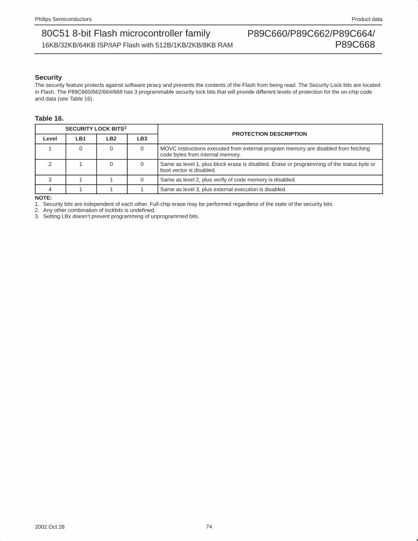
Philips Semiconductors Product data
P89C660/P89C662/P89C664/P89C668
80C51 8-bit Flash microcontroller family16KB/32KB/64KB ISP/IAP Flash with 512B/1KB/2KB/8KB RAM
2002 Oct 28 74
SecurityThe security feature protects against software piracy and prevents the contents of the Flash from being read. The Security Lock bits are locatedin Flash. The P89C660/662/664/668 has 3 programmable security lock bits that will provide different levels of protection for the on-chip codeand data (see Table 16).
Table 16.SECURITY LOCK BITS 1
PROTECTION DESCRIPTIONLevel LB1 LB2 LB3
PROTECTION DESCRIPTION
1 0 0 0 MOVC instructions executed from external program memory are disabled from fetchingcode bytes from internal memory.
2 1 0 0 Same as level 1, plus block erase is disabled. Erase or programming of the status byte orboot vector is disabled.
3 1 1 0 Same as level 2, plus verify of code memory is disabled.
4 1 1 1 Same as level 3, plus external execution is disabled.
NOTE:1. Security bits are independent of each other. Full-chip erase may be performed regardless of the state of the security bits.2. Any other combination of lockbits is undefined.3. Setting LBx doesn’t prevent programming of unprogrammed bits.

Philips Semiconductors Product data
P89C660/P89C662/P89C664/P89C668
80C51 8-bit Flash microcontroller family16KB/32KB/64KB ISP/IAP Flash with 512B/1KB/2KB/8KB RAM
2002 Oct 28 75
ABSOLUTE MAXIMUM RATINGS 1, 2, 3
PARAMETER RATING UNIT
Operating temperature under bias 0 to +70 or –40 to +85 °C
Storage temperature range –65 to +150 °C
Voltage on EA/VPP pin to VSS 0 to +13.0 V
Voltage on any other pin to VSS –0.5 to +6.5 V
Maximum IOL per I/O pin 15 mA
Power dissipation (based on package heat transfer limitations, not device power consumption) 1.5 W
NOTES:1. Stresses above those listed under Absolute Maximum Ratings may cause permanent damage to the device. This is a stress rating only and
functional operation of the device at these or any conditions other than those described in the AC and DC Electrical Characteristics sectionof this specification is not implied.
2. This product includes circuitry specifically designed for the protection of its internal devices from the damaging effects of excessive staticcharge. Nonetheless, it is suggested that conventional precautions be taken to avoid applying greater than the rated maximum.
3. Parameters are valid over operating temperature range unless otherwise specified. All voltages are with respect to VSS unless otherwise noted.

Philips Semiconductors Product data
P89C660/P89C662/P89C664/P89C668
80C51 8-bit Flash microcontroller family16KB/32KB/64KB ISP/IAP Flash with 512B/1KB/2KB/8KB RAM
2002 Oct 28 76
DC ELECTRICAL CHARACTERISTICSTamb = 0 °C to +70 °C, 5 V ± 10% or –40 °C to +85 °C; 5V ±5%; VSS = 0 V
SYMBOL PARAMETERTEST LIMITS
UNITSYMBOL PARAMETER CONDITIONS MIN TYP1 MAXUNIT
VIL Input low voltage 4.5 V < VCC < 5.5 V –0.5 0.2 VCC–0.1 V
VIL2 Input low voltage to P1.6/SCL, P1.7/SDA11 –0.5 0.3VDD V
VIH Input high voltage (ports 0, 1, 2, 3, EA) 0.2VCC+0.9 VCC+0.5 V
VIH1 Input high voltage, XTAL1, RST 0.7VCC VCC+0.5 V
VIH2 Input high voltage, P1.6/SCL, P1.7/SDA11 0.7VDD 6.0 V
VOL Output low voltage, ports 1, 2, 38 VCC = 4.5 VIOL = 1.6 mA2 – 0.4 V
VOL1 Output low voltage, port 0, ALE, PSEN 7, 8VCC = 4.5 V
IOL = 3.2 mA2 – 0.45 V
VOL2 Output low voltage, P1.6/SCL, P1.7/SDA IOL = 3.0 mA – 0.4 V
VOH Output high voltage, ports 1, 2, 3 3 VCC = 4.5 VIOH = –30 µA VCC – 0.7 – V
VOH1Output high voltage (port 0 in external bus mode),ALE9, PSEN3
VCC = 4.5 VIOH = –3.2 mA VCC – 0.7 – V
IIL Logical 0 input current, ports 1, 2, 3 VIN = 0.4 V –1 –75 µA
ITL Logical 1-to-0 transition current, ports 1, 2, 36 VIN = 2.0 VSee Note 4 – –650 µA
ILI Input leakage current, port 0 0.45 < VIN < VCC – 0.3 – ±10 µA
IL2 Input leakage current, P1.6/SCL, P1.7/SDA 0V < VI < 6 V0V < VDD < 5.5 V – 10 µA
ICC Power supply current (see Figure 64): See Note 5Active mode (see Note 5)Idle mode (see Note 5)Power-Down mode or clock stopped (see Figure 71
f diti )Tamb = 0 °C to 70 °C 20 100 µA
for conditions) Tamb = –40 °C to +85 °C 125 µAProgramming and erase mode fosc = 20 MHz 60 mA
RRST Internal reset pull-down resistor 40 225 kΩ
CIO Pin capacitance10 (except EA) – 15 pF
NOTES:1. Typical ratings are not guaranteed. The values listed are at room temperature, 5 V.2. Capacitive loading on ports 0 and 2 may cause spurious noise to be superimposed on the VOLs of ALE and ports 1 and 3. The noise is due
to external bus capacitance discharging into the port 0 and port 2 pins when these pins make 1-to-0 transitions during bus operations. In theworst cases (capacitive loading > 100 pF), the noise pulse on the ALE pin may exceed 0.8 V. In such cases, it may be desirable to qualifyALE with a Schmitt Trigger, or use an address latch with a Schmitt Trigger STROBE input. IOL can exceed these conditions provided that nosingle output sinks more than 5mA and no more than two outputs exceed the test conditions.
3. Capacitive loading on ports 0 and 2 may cause the VOH on ALE and PSEN to momentarily fall below the VCC–0.7 specification when theaddress bits are stabilizing.
4. Pins of ports 1, 2 and 3 source a transition current when they are being externally driven from 1 to 0. The transition current reaches itsmaximum value when VIN is approximately 2 V.
5. See Figures 68 through 71 for ICC test conditions and Figure 64 for ICC vs Freq. Active mode: ICC(MAX) = (2.8 × FREQ. + 8.0)mA for all devices, in 6 clock mode; (1.4 × FREQ. + 8.0)mA in 12 clock mode.Idle mode: ICC(MAX) = (1.2 × FREQ. +1.0)mA in 6 clock mode; (0.6 × FREQ. +1.0)mA in 12 clock mode.
6. This value applies to Tamb = 0 °C to +70 °C.7. Load capacitance for port 0, ALE, and PSEN = 100 pF, load capacitance for all other outputs = 80 pF.8. Under steady state (non-transient) conditions, IOL must be externally limited as follows:
Maximum IOL per port pin: 15 mA (*NOTE: This is 85 °C specification.)Maximum IOL per 8-bit port: 26 mAMaximum total IOL for all outputs: 71 mA
If IOL exceeds the test condition, VOL may exceed the related specification. Pins are not guaranteed to sink current greater than the listedtest conditions.
9. ALE is tested to VOH1, except when ALE is off then VOH is the voltage specification.10.Pin capacitance is characterized but not tested. Pin capacitance is less than 25 pF. Pin capacitance of ceramic package is less than 15 pF
(except EA is 25 pF).11. The input threshold voltage of P1.6 and P1.7 (SIO1) meets the I2C specification, so an input voltage below 1.5 V will be recognized as a logic 0
while an input voltage above 3.0 V will be recognized as a logic 1.

Philips Semiconductors Product data
P89C660/P89C662/P89C664/P89C668
80C51 8-bit Flash microcontroller family16KB/32KB/64KB ISP/IAP Flash with 512B/1KB/2KB/8KB RAM
2002 Oct 28 77
AC ELECTRICAL CHARACTERISTICS (6 CLOCK MODE)Tamb = 0 °C to +70 °C, VCC = 5 V ± 10% or –40 °C to +85 °C, VCC = 5 V ±5%, VSS = 0 V1, 2, 3
VARIABLE CLOCK 4 20 MHz CLOCK4
SYMBOL FIGURE PARAMETER MIN MAX MIN MAX UNIT
1/tCLCL 57 Oscillator frequency 0 20 – – MHz
tLHLL 57 ALE pulse width tCLCL–40 – 10 – ns
tAVLL 57 Address valid to ALE low 0.5tCLCL–20 – 5 – ns
tLLAX 57 Address hold after ALE low 0.5tCLCL–20 – 5 – ns
tLLIV 57 ALE low to valid instruction in – 2tCLCL–65 – 35 ns
tLLPL 57 ALE low to PSEN low 0.5tCLCL–20 – 5 – ns
tPLPH 57 PSEN pulse width 1.5tCLCL–45 – 30 – ns
tPLIV 57 PSEN low to valid instruction in – 1.5tCLCL–60 – 15 ns
tPXIX 57 Input instruction hold after PSEN 0 – 0 – ns
tPXIZ 57 Input instruction float after PSEN – 0.5tCLCL–20 – 5 ns
tAVIV 57 Address to valid instruction in – 2.5tCLCL–80 – 45 ns
tPLAZ 57 PSEN low to address float – 10 – 10 ns
Data Memory
tRLRH 58, 59 RD pulse width 3tCLCL–100 – 50 – ns
tWLWH 58, 59 WR pulse width 3tCLCL–100 – 50 – ns
tRLDV 58, 59 RD low to valid data in – 2.5tCLCL–90 – 35 ns
tRHDX 58, 59 Data hold after RD 0 – 0 – ns
tRHDZ 58, 59 Data float after RD – tCLCL–20 – 5 ns
tLLDV 58, 59 ALE low to valid data in – 4tCLCL–150 – 50 ns
tAVDV 58, 59 Address to valid data in – 4.5tCLCL–165 – 60 ns
tLLWL 58, 59 ALE low to RD or WR low 1.5tCLCL–50 1.5tCLCL+50 25 125 ns
tAVWL 58, 59 Address valid to WR low or RD low 2tCLCL–75 – 25 – ns
tQVWX 58, 59 Data valid to WR transition 0.5tCLCL–25 – 0 – ns
tWHQX 58, 59 Data hold after WR 0.5tCLCL–20 – 5 – ns
tQVWH 59 Data valid to WR high 3.5tCLCL–130 – 45 – ns
tRLAZ 58, 59 RD low to address float – 0 – 0 ns
tWHLH 58, 59 RD or WR high to ALE high 0.5tCLCL–20 0.5tCLCL+20 5 45 ns
External Clock
tCHCX 61 High time 20 tCLCL–tCLCX – – ns
tCLCX 61 Low time 20 tCLCL–tCHCX – – ns
tCLCH 61 Rise time – 5 – – ns
tCHCL 61 Fall time – 5 – – ns
Shift Register
tXLXL 60 Serial port clock cycle time 6tCLCL – 300 – ns
tQVXH 60 Output data setup to clock rising edge 5tCLCL–133 – 117 – ns
tXHQX 60 Output data hold after clock rising edge tCLCL–30 – 20 – ns
tXHDX 60 Input data hold after clock rising edge 0 – 0 – ns
tXHDV 60 Clock rising edge to input data valid – 5tCLCL–133 – 117 nsNOTES:1. Parameters are valid over operating temperature range unless otherwise specified.2. Load capacitance for port 0, ALE, and PSEN = 100 pF, load capacitance for all other outputs = 80 pF.3. Interfacing the microcontroller to devices with float times up to 45ns is permitted. This limited bus contention will not cause damage to Port 0 drivers.4. Parts are tested to 2 MHz, but are guaranteed to operate down to 0 Hz.

Philips Semiconductors Product data
P89C660/P89C662/P89C664/P89C668
80C51 8-bit Flash microcontroller family16KB/32KB/64KB ISP/IAP Flash with 512B/1KB/2KB/8KB RAM
2002 Oct 28 78
AC ELECTRICAL CHARACTERISTICS (6 CLOCK MODE) (Continued)Tamb = 0 °C to +70 °C, VCC = 5 V ± 10% or –40 °C to +85 °C,VCC = 5 V ± 5%, VSS = 0 V1, 2
SYMBOL PARAMETER INPUT OUTPUT
I2C Interface
tHD;STA START condition hold time ≥ 7 tCLCL > 4.0 µs 4
tLOW SCL low time ≥ 8 tCLCL > 4.7 µs 46
tHIGH SCL high time ≥ 7 tCLCL > 4.0 µs 4
tRC SCL rise time ≤ 1 µs – 5
tFC SCL fall time ≤ 0.3 µs < 0.3 µs 6
tSU;DAT1 Data set-up time ≥ 250 ns > 10 tCLCL – tRD
tSU;DAT2 SDA set-up time (before rep. START cond.) ≥ 250 ns > 1 µs 4
tSU;DAT3 SDA set-up time (before STOP cond.) ≥ 250 ns > 4 tCLCL
tHD;DAT Data hold time ≥ 0 ns > 4 tCLCL – tFC
tSU;STA Repeated START set-up time ≥ 7 tCLCL 4 > 4.7 µs 4
tSU;STO STOP condition set-up time ≥ 7 tCLCL 4 > 4.0 µs 4
tBUF Bus free time ≥ 7 tCLCL 4 > 4.7 µs 4
tRD SDA rise time ≤ 1 µs7 – 5
tFD SDA fall time ≤ 300 ns7 < 0.3 µs 6
NOTES:1. Parameters are valid over operating temperature range and voltage range unless otherwise specified.2. Load capacitance for port 0, ALE, and PSEN = 100 pF, load capacitance for all other outputs = 80 pF.3. These values are characterized but not 100% production tested.4. At 100 kbit/s. At other bit rates this value is inversely proportional to the bit-rate of 100 kbit/s.5. Determined by the external bus-line capacitance and the external bus-line pull-resistor, this must be < 1 µs.6. Spikes on the SDA and SCL lines with a duration of less than 3 tCLCL will be filtered out. Maximum capacitance on bus-lines SDA and
SCL = 400 pF.7. tCLCL = 1/fOSC = one oscillator clock period at pin XTAL1.

Philips Semiconductors Product data
P89C660/P89C662/P89C664/P89C668
80C51 8-bit Flash microcontroller family16KB/32KB/64KB ISP/IAP Flash with 512B/1KB/2KB/8KB RAM
2002 Oct 28 79
AC ELECTRICAL CHARACTERISTICS (12 CLOCK MODE)Tamb = 0 °C to +70 °C, VCC = 5 V ± 10%, or –40 °C to +85 °C, VCC = 5 V ±5%, VSS = 0V1, 2, 3
VARIABLE CLOCK 4 33 MHz CLOCK4
SYMBOL FIGURE PARAMETER MIN MAX MIN MAX UNIT
1/tCLCL 57 Oscillator frequency 0 33 – – MHz
tLHLL 57 ALE pulse width 2tCLCL–40 – 21 – ns
tAVLL 57 Address valid to ALE low tCLCL–25 – 5 – ns
tLLAX 57 Address hold after ALE low tCLCL–25 – 5 – ns
tLLIV 57 ALE low to valid instruction in – 4tCLCL–65 – 55 ns
tLLPL 57 ALE low to PSEN low tCLCL–25 – 5 – ns
tPLPH 57 PSEN pulse width 3tCLCL–45 – 45 – ns
tPLIV 57 PSEN low to valid instruction in – 3tCLCL–60 – 30 ns
tPXIX 57 Input instruction hold after PSEN 0 – 0 – ns
tPXIZ 57 Input instruction float after PSEN – tCLCL–25 – 5 ns
tAVIV 57 Address to valid instruction in – 5tCLCL–80 – 70 ns
tPLAZ 57 PSEN low to address float – 10 – 10 ns
Data Memory
tRLRH 58, 59 RD pulse width 6tCLCL–100 – 82 – ns
tWLWH 58, 59 WR pulse width 6tCLCL–100 – 82 – ns
tRLDV 58, 59 RD low to valid data in – 5tCLCL–90 – 60 ns
tRHDX 58, 59 Data hold after RD 0 – 0 – ns
tRHDZ 58, 59 Data float after RD – 2tCLCL–28 – 32 ns
tLLDV 58, 59 ALE low to valid data in – 8tCLCL–150 – 90 ns
tAVDV 58, 59 Address to valid data in – 9tCLCL–165 – 105 ns
tLLWL 58, 59 ALE low to RD or WR low 3tCLCL–50 3tCLCL+50 40 140 ns
tAVWL 58, 59 Address valid to WR low or RD low 4tCLCL–75 – 45 – ns
tQVWX 58, 59 Data valid to WR transition tCLCL–30 – 0 – ns
tWHQX 58, 59 Data hold after WR tCLCL–25 – 5 – ns
tQVWH 59 Data valid to WR high 7tCLCL–130 – 80 – ns
tRLAZ 58, 59 RD low to address float – 0 – 0 ns
tWHLH 58, 59 RD or WR high to ALE high tCLCL–25 tCLCL+25 5 55 ns
External Clock
tCHCX 61 High time 17 tCLCL–tCLCX – – ns
tCLCX 61 Low time 17 tCLCL–tCHCX – – ns
tCLCH 61 Rise time – 5 – – ns
tCHCL 61 Fall time – 5 – – ns
Shift Register
tXLXL 60 Serial port clock cycle time 12tCLCL – 360 – ns
tQVXH 60 Output data setup to clock rising edge 10tCLCL–133 – 167 – ns
tXHQX 60 Output data hold after clock rising edge 2tCLCL–80 – 50 – ns
tXHDX 60 Input data hold after clock rising edge 0 – 0 – ns
tXHDV 60 Clock rising edge to input data valid – 10tCLCL–133 – 167 nsNOTES:1. Parameters are valid over operating temperature range unless otherwise specified.2. Load capacitance for port 0, ALE, and PSEN = 100 pF, load capacitance for all other outputs = 80 pF.3. Interfacing the microcontroller to devices with float times up to 45 ns is permitted. This limited bus contention will not cause damage to Port 0
drivers.4. Parts are tested to 3.5 MHz, but guaranteed to operate down to 0 Hz.

Philips Semiconductors Product data
P89C660/P89C662/P89C664/P89C668
80C51 8-bit Flash microcontroller family16KB/32KB/64KB ISP/IAP Flash with 512B/1KB/2KB/8KB RAM
2002 Oct 28 80
AC ELECTRICAL CHARACTERISTICS (12 CLOCK MODE) (Continued)Tamb = 0°C to +70°C, VCC = 5 V ± 10%, or –40°C to +85°C, VCC = 5 V ± 5%, VSS = 0 V1, 2
SYMBOL PARAMETER INPUT OUTPUT
I2C Interface
tHD;STA START condition hold time ≥ 14 tCLCL > 4.0 µs 4
tLOW SCL low time ≥ 16 tCLCL > 4.7 µs 4
tHIGH SCL high time ≥ 14 tCLCL > 4.0 µs 4
tRC SCL rise time ≤ 1 µs – 5
tFC SCL fall time ≤ 0.3 µs < 0.3 µs 6
tSU;DAT1 Data set-up time ≥ 250 ns > 20 tCLCL – tRD
tSU;DAT2 SDA set-up time (before rep. START cond.) ≥ 250 ns > 1 µs 4
tSU;DAT3 SDA set-up time (before STOP cond.) ≥ 250 ns > 8 tCLCL
tHD;DAT Data hold time ≥ 0 ns > 8 tCLCL – tFC
tSU;STA Repeated START set-up time ≥ 14 tCLCL 4 > 4.7 µs 4
tSU;STO STOP condition set-up time ≥ 14 tCLCL 4 > 4.0 µs 4
tBUF Bus free time ≥ 14 tCLCL 4 > 4.7 µs 4
tRD SDA rise time ≤ 1 µs7 – 5
tFD SDA fall time ≤ 300 ns7 < 0.3 µs 6
NOTES:1. Parameters are valid over operating temperature range and voltage range unless otherwise specified.2. Load capacitance for port 0, ALE, and PSEN = 100 pF, load capacitance for all other outputs = 80 pF.3. These values are characterized but not 100% production tested.4. At 100 kbit/s. At other bit rates this value is inversely proportional to the bit-rate of 100 kbit/s.5. Determined by the external bus-line capacitance and the external bus-line pull-resistor, this must be < 1 µs.6. Spikes on the SDA and SCL lines with a duration of less than 3 tCLCL will be filtered out. Maximum capacitance on bus-lines SDA and
SCL = 400 pF.7. tCLCL = 1/fOSC = one oscillator clock period at pin XTAL1. For 63 ns < tCLCL < 285 ns (16 MHz > fOSC > 3.5 MHz) the I2C interface meets the
I2C-bus specification for bit-rates up to 100 kbit/s.

Philips Semiconductors Product data
P89C660/P89C662/P89C664/P89C668
80C51 8-bit Flash microcontroller family16KB/32KB/64KB ISP/IAP Flash with 512B/1KB/2KB/8KB RAM
2002 Oct 28 81
EXPLANATION OF THE AC SYMBOLSEach timing symbol has five characters. The first character is always‘t’ (= time). The other characters, depending on their positions,indicate the name of a signal or the logical status of that signal. Thedesignations are:A – AddressC – ClockD – Input dataH – Logic level highI – Instruction (program memory contents)L – Logic level low, or ALE
P – PSENQ – Output dataR – RD signalt – TimeV – ValidW– WR signalX – No longer a valid logic levelZ – FloatExamples: tAVLL = Time for address valid to ALE low.
tLLPL = Time for ALE low to PSEN low.
tPXIZ
ALE
PSEN
PORT 0
PORT 2 A0–A15 A8–A15
A0–A7 A0–A7
tAVLL
tPXIX
tLLAX
INSTR IN
tLHLL
tPLPHtLLIV
tPLAZ
tLLPL
tAVIV
SU00006
tPLIV
Figure 57. External Program Memory Read Cycle
ALE
PSEN
PORT 0
PORT 2
RD
A0–A7FROM RI OR DPL DATA IN A0–A7 FROM PCL INSTR IN
P2.0–P2.7 OR A8–A15 FROM DPF A0–A15 FROM PCH
tWHLH
tLLDV
tLLWL tRLRH
tLLAX
tRLAZ
tAVLL
tRHDX
tRHDZ
tAVWL
tAVDV
tRLDV
SU00025
Figure 58. External Data Memory Read Cycle

Philips Semiconductors Product data
P89C660/P89C662/P89C664/P89C668
80C51 8-bit Flash microcontroller family16KB/32KB/64KB ISP/IAP Flash with 512B/1KB/2KB/8KB RAM
2002 Oct 28 82
tLLAX
ALE
PSEN
PORT 0
PORT 2
WR
A0–A7FROM RI OR DPL DATA OUT A0–A7 FROM PCL INSTR IN
P2.0–P2.7 OR A8–A15 FROM DPF A0–A15 FROM PCH
tWHLH
tLLWL tWLWH
tAVLL
tAVWL
tQVWX tWHQX
tQVWH
SU00026
Figure 59. External Data Memory Write Cycle
0 1 2 3 4 5 6 7 8INSTRUCTION
ALE
CLOCK
OUTPUT DATA
WRITE TO SBUF
INPUT DATA
CLEAR RI
SET TI
SET RI
tXLXL
tQVXH
tXHQX
tXHDXtXHDV
SU00027
1 2 30 4 5 6 7
VALID VALID VALID VALID VALID VALID VALID VALID
Figure 60. Shift Register Mode Timing
VCC–0.5
0.45V0.7VCC
0.2VCC–0.1
tCHCL
tCLCL
tCLCHtCLCX
tCHCX
SU00009
Figure 61. External Clock Drive

Philips Semiconductors Product data
P89C660/P89C662/P89C664/P89C668
80C51 8-bit Flash microcontroller family16KB/32KB/64KB ISP/IAP Flash with 512B/1KB/2KB/8KB RAM
2002 Oct 28 83
VCC–0.5
0.45V
0.2VCC+0.9
0.2VCC–0.1
NOTE:AC inputs during testing are driven at VCC –0.5 for a logic ‘1’ and 0.45V for a logic ‘0’.Timing measurements are made at VIH min for a logic ‘1’ and VIL max for a logic ‘0’.
SU00717
Figure 62. AC Testing Input/Output
VLOAD
VLOAD+0.1V
VLOAD–0.1V
VOH–0.1V
VOL+0.1V
NOTE:
TIMINGREFERENCE
POINTS
For timing purposes, a port is no longer floating when a 100mV change fromload voltage occurs, and begins to float when a 100mV change from the loadedVOH/VOL level occurs. IOH/IOL ≥ ±20mA.
SU00718
Figure 63. Float Waveform
2 4 6 8 10 12 14 16 18
60
50
40
30
20
10
Frequency at XTAL1 (MHz, 6 clock mode)
ICC (mA)
89C660/662/664/668MAXIMUM ACTIVE ICC
TYPICAL ACTIVE ICC
MAXIMUM IDLE
TYPICAL IDLE
SU01402
20
70
Figure 64. I CC vs. FREQValid only within frequency specifications of the device under test

Philips Semiconductors Product data
P89C660/P89C662/P89C664/P89C668
80C51 8-bit Flash microcontroller family16KB/32KB/64KB ISP/IAP Flash with 512B/1KB/2KB/8KB RAM
2002 Oct 28 84
tRD
tSU;STA
tBUF
tSU;STO
0.7 VCC
0.3 VCC
0.7 VCC
0.3 VCC
tFD tRC tFC
tHIGHtLOWtHD;STA tSU;DAT1 tHD;DAT tSU;DAT2
tSU;DAT3
START conditionrepeated START condition
SDA(INPUT/OUTPUT)
SCL(INPUT/OUTPUT)
STOP condition
START or repeated START condition
SU00107A
Figure 65. Timing SI01 (I 2C) Interface
VCC–0.5
0.45V
0.2VCC+0.9
0.2VCC–0.1
NOTE:AC inputs during testing are driven at VCC –0.5 for a logic ‘1’ and 0.45V for a logic ‘0’.Timing measurements are made at VIH min for a logic ‘1’ and VIL max for a logic ‘0’.
SU00010
Figure 66. AC Testing Input/Output
VLOAD
VLOAD+0.1V
VLOAD–0.1V
VOH–0.1V
VOL+0.1V
NOTE:
TIMINGREFERENCE
POINTS
For timing purposes, a port is no longer floating when a 100mV change from load voltage occurs,and begins to float when a 100mV change from the loaded VOH/VOL level occurs. IOH/IOL ≥ ±20mA.
SU00011
Figure 67. Float Waveform

Philips Semiconductors Product data
P89C660/P89C662/P89C664/P89C668
80C51 8-bit Flash microcontroller family16KB/32KB/64KB ISP/IAP Flash with 512B/1KB/2KB/8KB RAM
2002 Oct 28 85
VCC
P0
EA
RST
XTAL1
XTAL2
VSS
VCC
VCC
VCC
ICC
(NC)
CLOCK SIGNAL
P1.6
P1.7
*
*
89C66089C66289C66489C668
SU01261
Figure 68. I CC Test Condition, Active Mode.All other pins are disconnected
VCC
P0
RST
XTAL1
XTAL2
VSS
VCC
VCC
ICC
(NC)
CLOCK SIGNAL
P1.6
P1.7
EA
*
*
89C66089C66289C66489C668
SU01262
Figure 69. I CC Test Condition, Idle Mode.All other pins are disconnected
VCC–0.5
0.5V
tCHCL
tCLCL
tCLCHtCLCX
tCHCX
SU00266
Figure 70. Clock Signal Waveform for I CC Tests in Active and Idle Modes.tCLCL = tCHCL = 10 ns
VCC
P0
RST
XTAL1
XTAL2
VSS
VCC
VCC
ICC
(NC) P1.6
P1.7
EA
**
89C66089C66289C66489C668
SU01263
Figure 71. I CC Test Condition, Power-Down mode.All other pins are disconnected; V CC = 2V to 5.5V
NOTE:* Ports 1.6 and 1.7 should be connected to VCC through resistors of sufficiently high value such that the sink current into these pins does not
exceed the IOL1 specification.

Philips Semiconductors Product data
P89C660/P89C662/P89C664/P89C668
80C51 8-bit Flash microcontroller family16KB/32KB/64KB ISP/IAP Flash with 512B/1KB/2KB/8KB RAM
2002 Oct 28 86
PLCC44: plastic leaded chip carrier; 44 leads SOT187-2
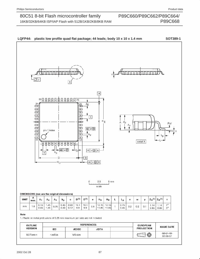
Philips Semiconductors Product data
P89C660/P89C662/P89C664/P89C668
80C51 8-bit Flash microcontroller family16KB/32KB/64KB ISP/IAP Flash with 512B/1KB/2KB/8KB RAM
2002 Oct 28 87
LQFP44: plastic low profile quad flat package; 44 leads; body 10 x 10 x 1.4 mm SOT389-1

Philips Semiconductors Product data
P89C660/P89C662/P89C664/P89C668
80C51 8-bit Flash microcontroller family16KB/32KB/64KB ISP/IAP Flash with 512B/1KB/2KB/8KB RAM
2002 Oct 28 88
REVISION HISTORY
Rev Date Description
_4 20021028 Product data (9397 750 10403); replaces P89C660/P89C662/P89C664 of 2001 Jul 19(9397 750 08584) and P89C668 of 2001 Jul 27 (9397 750 08651)
Engineering Change Notice 853–2392 29118 (date: 20021028)
Modifications:
• Integrated 89C668 in 89C66x datasheet
• Added more description on I2C, Timer 0 and Timer 1, and Enhanced UART
• P2.6 must be high to activate the boot loader by hardware (ISP section).

Philips Semiconductors Product data
P89C660/P89C662/P89C664/P89C668
80C51 8-bit Flash microcontroller family16KB/32KB/64KB ISP/IAP Flash with 512B/1KB/2KB/8KB RAM
2002 Oct 28 89
DefinitionsShort-form specification — The data in a short-form specification is extracted from a full data sheet with the same type number and title. For detailed information seethe relevant data sheet or data handbook.
Limiting values definition — Limiting values given are in accordance with the Absolute Maximum Rating System (IEC 60134). Stress above one or more of the limitingvalues may cause permanent damage to the device. These are stress ratings only and operation of the device at these or at any other conditions above those givenin the Characteristics sections of the specification is not implied. Exposure to limiting values for extended periods may affect device reliability.
Application information — Applications that are described herein for any of these products are for illustrative purposes only. Philips Semiconductors make norepresentation or warranty that such applications will be suitable for the specified use without further testing or modification.
DisclaimersLife support — These products are not designed for use in life support appliances, devices, or systems where malfunction of these products can reasonably beexpected to result in personal injury. Philips Semiconductors customers using or selling these products for use in such applications do so at their own risk and agreeto fully indemnify Philips Semiconductors for any damages resulting from such application.
Right to make changes — Philips Semiconductors reserves the right to make changes in the products—including circuits, standard cells, and/or software—describedor contained herein in order to improve design and/or performance. When the product is in full production (status ‘Production’), relevant changes will be communicatedvia a Customer Product/Process Change Notification (CPCN). Philips Semiconductors assumes no responsibility or liability for the use of any of these products, conveysno license or title under any patent, copyright, or mask work right to these products, and makes no representations or warranties that these products are free from patent,copyright, or mask work right infringement, unless otherwise specified.
Contact informationFor additional information please visithttp://www.semiconductors.philips.com . Fax: +31 40 27 24825
For sales offices addresses send e-mail to:[email protected] .
Koninklijke Philips Electronics N.V. 2002All rights reserved. Printed in U.S.A.
Date of release: 10-02
Document order number: 9397 750 10403
Data sheet status [1]
Objective data
Preliminary data
Product data
Productstatus [2] [3]
Development
Qualification
Production
Definitions
This data sheet contains data from the objective specification for product development.Philips Semiconductors reserves the right to change the specification in any manner without notice.
This data sheet contains data from the preliminary specification. Supplementary data will be publishedat a later date. Philips Semiconductors reserves the right to change the specification without notice, inorder to improve the design and supply the best possible product.
This data sheet contains data from the product specification. Philips Semiconductors reserves theright to make changes at any time in order to improve the design, manufacturing and supply. Relevantchanges will be communicated via a Customer Product/Process Change Notification (CPCN).
Data sheet status
[1] Please consult the most recently issued data sheet before initiating or completing a design.
[2] The product status of the device(s) described in this data sheet may have changed since this data sheet was published. The latest information is available on the Internet at URLhttp://www.semiconductors.philips.com.
[3] For data sheets describing multiple type numbers, the highest-level product status determines the data sheet status.
Level
I
II
III