P517/617 Lec7, P1 Transistors and Amplifiers - Physics |gan/teaching/sum… · ·...
9
P517/617 Lec7, P1 Transistors and Amplifiers Hybrid Transistor Model for Small AC Signals The previous model for a transistor used one parameter (b, the current gain) to describe the transistor. This model is naive and doesn't explain many of the features of the three common forms of transistor amplifiers (common emitter etc.) For example, we could not calculate the output impedance of the common emitter amp with the one parameter model. Very often in electronics we describe complex circuits in terms of an equivalent circuit or model. For the transistor we wish to have a model that relates the input currents and voltages to the output currents and voltages. We also wish this model to be linear in the currents and voltages. For a transistor this condition of linearity is true for small signals. The most general linear model of the transistor is a 4-terminal "black box". In this model we assume that the transistor is biased on properly and often we do not even show the biasing circuit. For the transistor where there are only 3 legs, one of the terminals is common between the input and output. T V V I I o o i i There are 4 variables in the problem, I i , V i , I o , and V o . The subscript i refer to the input side while the subscript o refers to the output side. We now assume that we know I i and V o . Kirchhoff's laws relate all the currents and voltages: V i = V i I i , V o ( ) I o = I o I i , V o ( ) Since we have a linear model of the transistor we can write the following for small changes in I i and V o : dV i = ∂ V i ∂ I i Ê Ë Á ˆ ¯ ˜ V o dI i + ∂V i ∂ V o Ê Ë Á ˆ ¯ ˜ I i dV o dI o = ∂ I o ∂ I i Ê Ë Á ˆ ¯ ˜ V o dI i + ∂ I o ∂ V o Ê Ë Á ˆ ¯ ˜ I i dV o
Transcript of P517/617 Lec7, P1 Transistors and Amplifiers - Physics |gan/teaching/sum… · ·...

P517/617 Lec7, P1Transistors and Amplifiers
Hybrid Transistor Model for Small AC SignalsThe previous model for a transistor used one parameter (b, the current gain) to describe the
transistor. This model is naive and doesn't explain many of the features of the three common formsof transistor amplifiers (common emitter etc.) For example, we could not calculate the outputimpedance of the common emitter amp with the one parameter model.
Very often in electronics we describe complex circuits in terms of an equivalent circuit ormodel. For the transistor we wish to have a model that relates the input currents and voltages to theoutput currents and voltages. We also wish this model to be linear in the currents and voltages.For a transistor this condition of linearity is true for small signals.
The most general linear model of the transistor is a 4-terminal "black box".In this model we assume that the transistor is biased on properly and often we do not even
show the biasing circuit.For the transistor where there are only 3 legs, one of the terminals is common between the
input and output.
Ø
T
Ø
V V
I Io
oi
i
There are 4 variables in the problem, Ii, Vi, Io, and Vo. The subscript i refer to the input sidewhile the subscript o refers to the output side. We now assume that we know Ii and Vo.Kirchhoff's laws relate all the currents and voltages:
Vi = Vi Ii ,Vo( )Io = Io Ii ,Vo( )
Since we have a linear model of the transistor we can write the following for small changes inIi and Vo:
dVi =∂Vi∂Ii
Ê
Ë Á ˆ
¯ ˜
Vo
dIi +∂V i∂Vo
Ê
Ë Á ˆ
¯ ˜
I i
dVo
dIo =∂Io∂Ii
Ê
Ë Á ˆ
¯ ˜
Vo
dIi +∂Io∂Vo
Ê
Ë Á ˆ
¯ ˜
Ii
dVo
P517/617 Lec7, P2The partial derivatives are called the hybrid (or h) parameters. We rewrite the above equations as:
dV i = hi idI i + hiodVodIo = hoidIi + hoodVo
The parameters hoi and hio are unitless while hoo has units 1/W (mhos) and hi i has units W.
The four h parameters are easily measured. For example to measure hii hold Vo (the outputvoltage) constant and measure Vin/Iin. Unfortunately the h parameters are not constant. Forexample Figs. 11-14 of the 2N3904 spec sheet show the variation of the four parameters withcollector current (IC).
There are 3 sets of the 4 hybrid parameters, one for each type of amp (common emitter,common base, common collector). In order to differentiate one set of parameters from another thefollowing notation is used:
First subscript Second subscripti = input impedance e = common emittero = output admittance b = common baser = reverse voltage ratio c = common collectorf = forward current ratio
Thus for a common emitter amplifier we would write:dV i = hiedIi + hredVodIo = hfedI i + hoedVo
Typical values for the h parameters for a 2N3904 transistor in the common emitter configurationwith IC = 1 mA are as follows:
hfe = 120, hoe = 8.7x10⁻⁶ W-1, hie = 3700 W, hre = 1.3x10⁻⁴
The equivalent circuit for a transistor in the common emitter configuration looks like:
emitter
base collector
Ø
Ø
V V
I I
VIi
i
o
o
h
hh ho ire
ie
fe oe1/ Ø
The circle is a voltage source, i.e. the voltage across this element is always equal to hreVo
independent of the current through it. The triangle is a current source, the current through thiselement is always hfeIin independent of the voltage across the device.
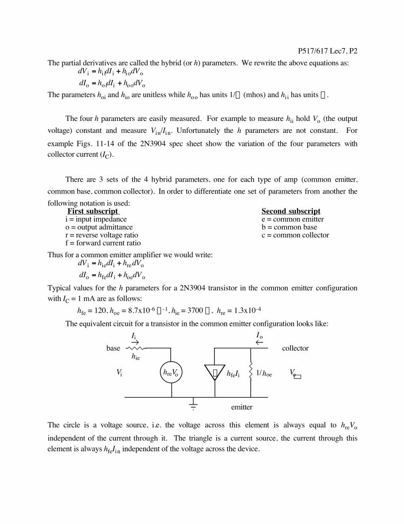
P517/617 Lec7, P3We can calculate the voltage and current gain, and the input and output impedance of a
common emitter amp using this model. Below is the equivalent circuit (without biasing network)for a CE amp attached to a voltage source (with resistance Rs) and load resistor (Rload).
emitter
base collector
Ø
Ø
Ø
VV
I I
VIi
i
o
o
h
hh ho ire
ie
fe oe1/R
Rs
load
Current gain: The current gain (GI) is defined as: GI = Io/Iin.Using Kirchhoff's current law at the output side we have:
hfeIin + Vohoe = Io
Using Kirchhoff's voltage rule at the output we have:Vo = - IoRload
Putting the two equations together we get:hfeIin = hoeIoRload + IoGI = Io / Iin = hfe / (1+ hoeRload)
For typical CE amps, hoeRload << 1 and the gain reduces to familiar form:GI ª hfe = b
Voltage gain: The voltage gain (Gv) is defined as: Gv = Vo/Vin.
This gain can be derived in a similar fashion as the current gain. The result is:GV = Vo / Vin = -hfeRload / (DRload + hie)
with D = hiehoe - hfehre ª10-2
This reduces to a familiar form for most cases where DRload << hieGV = -hfe Rload / hie = -Rload / rBE
Input Impedance: The input impedance (Zi) is defined as: Zi = Vin/Iin.Zi = (DRload + hie) / (1 + hoeRload)
This reduces to a familiar form for most cases where DRload << hie and hoe Rload << 1Zi = hie = hferBE
Output Impedance: The output impedance (Zo) is defined as: Zo = Vo/Io.Zo = (Rs + hie) / (D + hoeRs )
Zo does not reduce to a simple expression. As the denominator is small, Zo is as advertised large.
P517/617 Lec7, P4
Feedback and Amplifiers
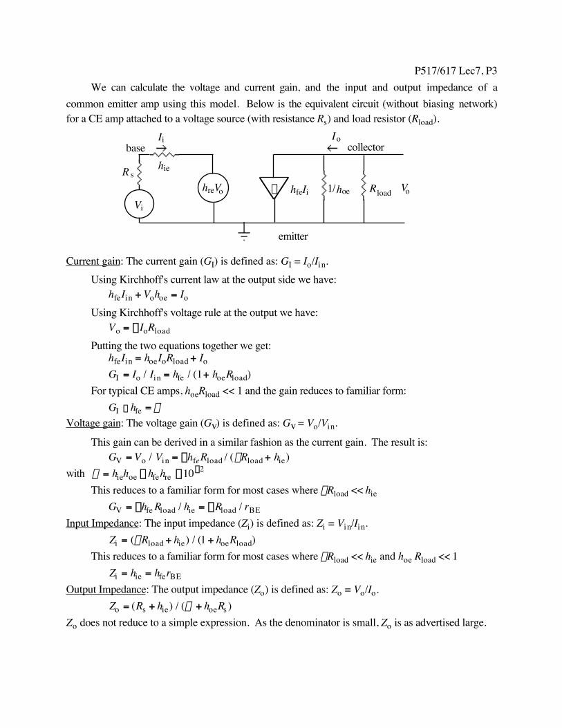
• Consider the following common emitter amplifier:
V
V
Vout
B
cc
1
1
2
3 E
R
R
RR
Q
This amp differs slightly from the CE amp we saw before in that the bias resistor R2 isconnected to the collector resistor R1 instead of directly to Vcc.
•How does this effect Vout?a) If Vout decreases (moves away from Vcc) then I2 increases which means that VB decreases (getscloser to ground). However, if VB decreases, then Vout will increase since DVout = -DVB R1/RE.b) If Vout increases (moves towards Vcc) then I2 decreases which means that VB increases (movesaway from ground). However, if VB increases, then Vout will decrease since DVout = -DVB R1/RE.
This is an example of NEGATIVE FEEDBACK
Negative Feedback is good:Stabilizes amplifier against oscillationIncreases the input impedance of the amplifierDecreases the output impedance of the amplifier
Positive Feedback is bad:Causes amplifiers to oscillate.
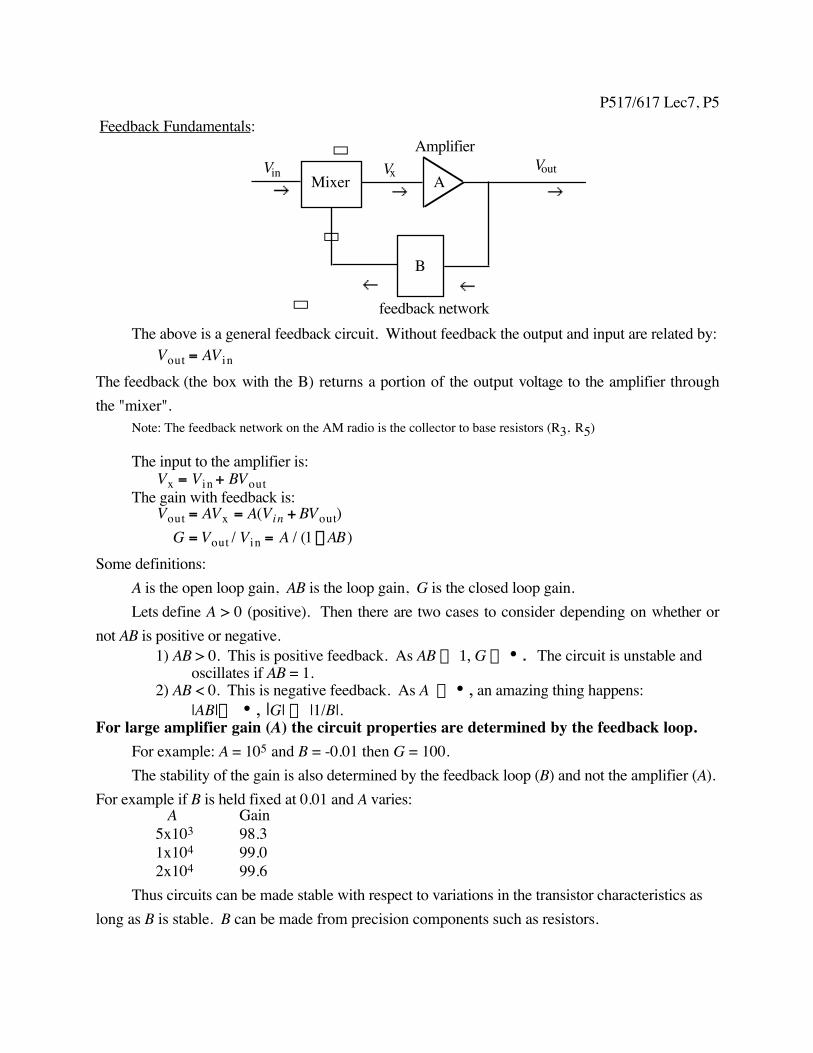
P517/617 Lec7, P5 Feedback Fundamentals:
Mixer A
B
feedback network
AmplifierØ
Ø
Ø
Ø
Ø
VV Vin outx
The above is a general feedback circuit. Without feedback the output and input are related by:Vout = AV in
The feedback (the box with the B) returns a portion of the output voltage to the amplifier throughthe "mixer". Note: The feedback network on the AM radio is the collector to base resistors (R3, R5)
The input to the amplifier is:Vx = Vin + BVout
The gain with feedback is:Vout = AVx = A(Vin + BVout)
G = Vout / Vin = A / (1 - AB)Some definitions:
A is the open loop gain, AB is the loop gain, G is the closed loop gain.Lets define A > 0 (positive). Then there are two cases to consider depending on whether or
not AB is positive or negative.1) AB > 0. This is positive feedback. As AB Æ 1, G Æ •. The circuit is unstable and
oscillates if AB = 1.2) AB < 0. This is negative feedback. As A Æ •, an amazing thing happens:
|AB|Æ •, |G| Æ |1/B|.For large amplifier gain (A) the circuit properties are determined by the feedback loop.
For example: A = 105 and B = -0.01 then G = 100.The stability of the gain is also determined by the feedback loop (B) and not the amplifier (A).
For example if B is held fixed at 0.01 and A varies: A Gain5x103 98.31x10⁴ 99.02x10⁴ 99.6
Thus circuits can be made stable with respect to variations in the transistor characteristics aslong as B is stable. B can be made from precision components such as resistors.

P517/617 Lec7, P6Operational Amplifiers (Op Amps)
• Op amps are very high gain (A = 105) differential amplifiers.A differential amp has two inputs (V1, V2) and output Vout = A(V1 - V2 ) where A is the
amplifier gain.
-+non inverting input
inverting input (power connections not shown)
Vout
If an op amp is used without feedback and V1 ≠ V2 , then Vout saturates at the power supplyvoltage (either positive or negative supply).
• Op amps are almost always used with negative feedback. The output is connected to the(inverting) input.
• Op amps come in "chip" form. They are made up of complex circuits with 20-100 transistors.Ideal Op Amp Real Op Amp mA741
Voltage gain (open loop) • 105
Input impedance • 2 MWOutput impedance 0 75 WSlew rate* • 0.5 V/msecPower consumption 0 50 mWVout with Vin = 0 0 2 mV (unity gain)Price 0$ $0.25* slew rate is how fast the output can change
• When working with op amps using negative feedback the following two simple rules (almost)always apply:
1) No current goes into the op amp.2) Both input terminals of the op amp have the same voltage.
The first rule reflects the high input impedance of the op amp. The second rule has to do withthe actual circuitry making up the op amp.• Some examples of op amp circuits with negative feedback:Voltage Follower
-+
(power connections not shown)V
Vinout =Vin
The feedback network is just a wire connecting the output to the input. By rule #2, theinverting (-) input is also at Vin. Thus Vout = Vin.
What good is this circuit? It is mainly used as a buffer as it has high input impedance (MW)and low output impedance (100 W).

P517/617 Lec7, P7Inverting Amplifier:
-+
(power connections not shown)VV
R
Ain
1
f
out
R
By rule #2, point A is at ground.By Rule #1, no current is going into the op amp.We can redraw the circuit as:
Ø
ØV V
Rin
1 fout
R
IoutI in
Vin / R1 + Vout / Rf = 0Vout / Vin = -Rf / R1
Thus the closed loop gain is Rf/R1. The minus sign in the gain means that the output has theopposite polarity as the input. See page 8 for more details.
Non-Inverting Amplifier:
-+
(power connections not shown)
VV
R
Ain
1
f
out
R
By rule #2, point A is Vin.By Rule #1, no current is going into the op amp. We can redraw the circuit as:
Ø
VV
R
in
1 fout
R
IoutI inx
Ø
Vin / R1 + (V in - Vout) / Rf = 0Vout / Vin = (R1 + Rf ) / R1
Thus the closed loop gain is (R1 + Rf ) / R1. For this circuit the output has the same polarityas the input.
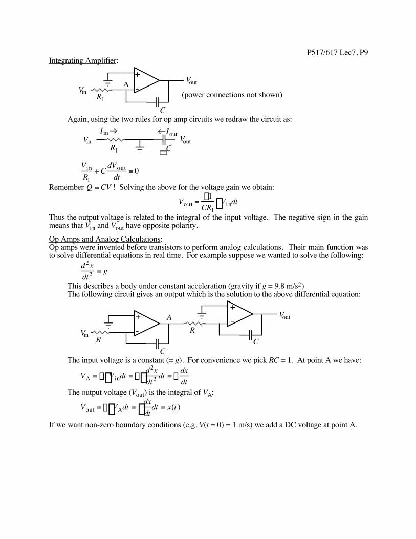
P517/617 Lec7, P9Integrating Amplifier:
-
+
(power connections not shown)AV
Vin
1
out
RC
Again, using the two rules for op amp circuits we redraw the circuit as:
Ø
Ø
V Vin1
outR
IoutI in
C
VinR1
+ C dVoutdt
= 0
Remember Q = CV ! Solving the above for the voltage gain we obtain:
Vout =-1
CR1VinÚ dt
Thus the output voltage is related to the integral of the input voltage. The negative sign in the gainmeans that Vin and Vout have opposite polarity.Op Amps and Analog Calculations:Op amps were invented before transistors to perform analog calculations. Their main function wasto solve differential equations in real time. For example suppose we wanted to solve the following:
d2 xdt2 = g
This describes a body under constant acceleration (gravity if g = 9.8 m/s2)The following circuit gives an output which is the solution to the above differential equation:
-
+
R
A
C
-+
RC
V
V
in
out
The input voltage is a constant (= g). For convenience we pick RC = 1. At point A we have:
VA = - VinÚ dt = -d2xdt2Ú dt = -
dxdt
The output voltage (Vout) is the integral of VA:
Vout = - VAÚ dt =dxdtÚ dt = x(t )
If we want non-zero boundary conditions (e.g. V(t = 0) = 1 m/s) we add a DC voltage at point A.