Oxidationelectronics:bond–band–barrier ... ·...
165
Oxidation electronics: bond–band–barrier correlation and its applications § Chang Q. Sun* School of Electrical and Electronic Engineering, Block S2, Nanyang Technological University, Singapore 639798, Singapore Institute of Advanced Materials Physics and Faculty of Science, Tianjin University, 300072, China Abstract This report features the recent progress in understanding the behaviour of atoms and valence electrons involved in the process of oxidation, and some technological development driven by the new knowledge. It is initiated and verified that a chemical bond contracts spontaneously at a surface associated with magnitude rise of the bond energy due to the coordination imperfection and that an oxygen atom hybridizes its sp orbitals upon reacting with a solid surface. The former leads to the bond order–length–strength (BOLS) correlation for the physical aspect of a surface and a nano-solid and the latter to a bond–band–barrier (BBB) correlation for chemical reaction. In the process of oxidation, non-bonding lone pairs, anti-bonding dipoles and hydrogen-like bonds are involved, which add corresponding density- of-states (DOS) features to the valence band of the host. Bond forming also alters the sizes and valencies of the involved atoms and causes a collective dislocation of these atoms, which corrugate the morphology or the potential barrier of the surface. Based on the above pre- mises, the oxidation of the low-index surfaces of transition metals Cu, Co, Ag and V, noble metals Rh, Ru, and Pd and non-metallic diamond has been consistently analyzed. Identities probed with various techniques, such as STM, LEED, XRD, STS, PES, TDS, EELS and Raman, have been systematically defined in terms of atomic valencies, bond geometry, valence DOS, bond strength and bond forming kinetics. It is understood that formation of the basic oxide tetrahedron, and consequently, the four discrete stages of bond forming kinetics and the oxygen-derived DOS features, are intrinsically common for all the analyzed systems though the patterns of observations may vary from situation to situation. What differs one oxide surface from another in observations are: (i) the site selectivity of the oxygen adsorbate, (ii) the order of the ionic bond formation and, (iii) the orientation of the tetrahedron at the host surfaces. The valencies of oxygen, the scale and geometrical orientation of the host lattice and the electronegativity of the host elements determine these specific differences extrinsically. Progress in Materials Science 48 (2003) 521–685 www.elsevier.com/locate/pmatsci 0079-6425/03/$ - see front matter # 2003 Elsevier Ltd. All rights reserved. doi:10.1016/S0079-6425(03)00010-0 § Supplementary multimedia movie showing the quantified four-stage Cu 3 O 2 bonding kinetics can be found at doi:10.1016/S0079-6425(03)00010-0. * Tel.: +65-6790-4517; fax: +65-6792-0415. E-mail addresses: [email protected] (C.Q. Sun).
Transcript of Oxidationelectronics:bond–band–barrier ... ·...

Oxidation electronics: bond–band–barriercorrelation and its applications§
Chang Q. Sun*
School of Electrical and Electronic Engineering, Block S2, Nanyang Technological University,
Singapore 639798, Singapore
Institute of Advanced Materials Physics and Faculty of Science, Tianjin University, 300072, China
Abstract
This report features the recent progress in understanding the behaviour of atoms and
valence electrons involved in the process of oxidation, and some technological developmentdriven by the new knowledge. It is initiated and verified that a chemical bond contractsspontaneously at a surface associated with magnitude rise of the bond energy due to the
coordination imperfection and that an oxygen atom hybridizes its sp orbitals upon reactingwith a solid surface. The former leads to the bond order–length–strength (BOLS) correlationfor the physical aspect of a surface and a nano-solid and the latter to a bond–band–barrier
(BBB) correlation for chemical reaction. In the process of oxidation, non-bonding lone pairs,anti-bonding dipoles and hydrogen-like bonds are involved, which add corresponding density-of-states (DOS) features to the valence band of the host. Bond forming also alters the sizesand valencies of the involved atoms and causes a collective dislocation of these atoms, which
corrugate the morphology or the potential barrier of the surface. Based on the above pre-mises, the oxidation of the low-index surfaces of transition metals Cu, Co, Ag and V, noblemetals Rh, Ru, and Pd and non-metallic diamond has been consistently analyzed. Identities
probed with various techniques, such as STM, LEED, XRD, STS, PES, TDS, EELS andRaman, have been systematically defined in terms of atomic valencies, bond geometry,valence DOS, bond strength and bond forming kinetics. It is understood that formation of the
basic oxide tetrahedron, and consequently, the four discrete stages of bond forming kineticsand the oxygen-derived DOS features, are intrinsically common for all the analyzed systemsthough the patterns of observations may vary from situation to situation. What differs oneoxide surface from another in observations are: (i) the site selectivity of the oxygen adsorbate,
(ii) the order of the ionic bond formation and, (iii) the orientation of the tetrahedron at thehost surfaces. The valencies of oxygen, the scale and geometrical orientation of the host latticeand the electronegativity of the host elements determine these specific differences extrinsically.
Progress in Materials Science 48 (2003) 521–685
www.elsevier.com/locate/pmatsci
0079-6425/03/$ - see front matter # 2003 Elsevier Ltd. All rights reserved.
doi:10.1016/S0079-6425(03)00010-0
§ Supplementary multimedia movie showing the quantified four-stage Cu3O2 bonding kinetics can be
found at doi:10.1016/S0079-6425(03)00010-0.
* Tel.: +65-6790-4517; fax: +65-6792-0415.
E-mail addresses: [email protected] (C.Q. Sun).

Extending the premise of sp-orbital hybridization to the reactions of (C, N)–Ni(001) surfaces
has led to a novel approach neutralizing the diamond–metal interfacial stress and hencestrengthening the diamond–metal adhesion substantially. The BOLS correlation has providedconsistent insight into the shape-and-size dependence of a number of properties for nano-
solids. The BBB correlation has led to new findings in designing and fabricating materials forphotoluminescence, electron emission and ultrahigh elasticity, etc.# 2003 Elsevier Science Ltd. All rights reserved.
Keywords: Surface interface; Crystal growth; Chemisorption; Materials design; Oxygen
Contents
1. Introduction ....................................................................................................................525
1.1. Scope ......................................................................................................................5251.2. Overview.................................................................................................................5261.3. Challenges...............................................................................................................528
1.3.1. Bond nature and bond forming kinetics.....................................................5281.3.2. Alteration of atomic valencies ....................................................................5291.3.3. Spectroscopes correspondences ..................................................................529
1.3.4. Driving forces behind reconstruction .........................................................5301.3.5. Work function and inner potential change.................................................5321.3.6. Factors controlling bond formation...........................................................532
1.4. Objectives ...............................................................................................................533
2. Principle: bond–band–barrier (BBB) correlation ............................................................5342.1. Foundations ...........................................................................................................534
2.1.1. Basic concepts.............................................................................................5342.1.2. Bonding effects ........................................................................................... 536
2.2. Chemical bond: the basic tetrahedron....................................................................539
2.3. Valence density-of-state (DOS) ..............................................................................5422.4. Surface potential barrier (SPB) ..............................................................................543
2.4.1. One-dimensional SPB model ......................................................................543
2.4.2. 3-D effect with DOS contribution ..............................................................5452.4.3. Physical indications ....................................................................................545
2.5. Summary ................................................................................................................546
3. STM and LEED: atomic valencies and bond geometry..................................................5473.1. Phase ordering ........................................................................................................5473.2. O–Cu{(001), (110), (111)}....................................................................................... 548
3.2.1. Observations............................................................................................... 5483.2.2. Analysis ......................................................................................................5563.2.3. Quantification: bond geometry and bonding kinetics ................................561
3.2.4. Summary ....................................................................................................5683.3. O–(Rh, Pd)(110) .....................................................................................................570
3.3.1. Observations............................................................................................... 570
3.3.2. Analysis ......................................................................................................5733.4. O–(Co, Ru)(101
-0) ...................................................................................................576
3.4.1. Observations............................................................................................... 5763.4.2. Analysis ......................................................................................................577
522 C.Q. Sun / Progress in Materials Science 48 (2003) 521–685

3.5. O–Rh(111) and O–Ru(0001) .................................................................................. 584
3.5.1. Observations............................................................................................... 5843.5.2. Analysis ......................................................................................................586
3.6. O–Rh(001) and (N, C)–Ni(001)..............................................................................590
3.6.1. Observations............................................................................................... 5903.6.2. Analysis ......................................................................................................5943.6.3. Quantification: driving force and bond stress ............................................597
3.7. O–(Ag, V)(001) .......................................................................................................599
3.7.1. O–Ag(001) ..................................................................................................5993.7.2. O–V(001) ....................................................................................................601
4. STS and PES: valence DOS ............................................................................................ 6044.1. Signature generality ................................................................................................ 604
4.1.1. STS .............................................................................................................604
4.1.2. PES, IPES and XPS ...................................................................................6064.1.3. Indication ...................................................................................................611
4.2. Specification ...........................................................................................................611
5. TDS: bond nature and bond strength .............................................................................6125.1. Identity similarity ...................................................................................................6125.2. Specification ...........................................................................................................618
6. EELS and Raman: fingerprints of weak interaction .......................................................6196.1. EELS: dipole vibration........................................................................................... 619
6.2. Raman: lone-pair in oxides, nitrides and bio-molecules.........................................6206.3. Confirmation: ultra-elasticity of nitride surfaces ....................................................620
7. Kinetics of bond forming and bond switching................................................................6227.1. Four-stage bond forming kinetics ..........................................................................6227.2. Bond switching: O-floating and O-diffusing ...........................................................624
8. Application: I. Bond contraction and charge transport ..................................................6258.1. Introduction ...........................................................................................................6258.2. Nano-solid: bond order–length–strength (BOLS) correlation................................626
8.2.1. Principle......................................................................................................6278.2.2. Application: lattice strain and surface mechanics ......................................6288.2.3. Other applications ...................................................................................... 634
8.3. Catalytic effect on band-gap expansion..................................................................6368.3.1. Blue light emission of PZT.........................................................................6368.3.2. O-induced blue-shift in PL .........................................................................6398.3.3. PL of III- and IV-nitride ............................................................................641
8.4. Joint size and catalytic effects: PL of nanometric SiO2 ..........................................6428.5. Work function reduction: cold cathode field emission ...........................................647
8.5.1. Current understanding ...............................................................................647
8.5.2. Explanation ................................................................................................ 6498.6. Magnetic enhancement ........................................................................................... 649
9. Application: II. Synthetic diamond.................................................................................6509.1. Thermal oxidation ..................................................................................................651
C.Q. Sun / Progress in Materials Science 48 (2003) 521–685 523
Nomenclature
� ElectronegativityY (ML) Oxygen coverage (unit in Monolayer)gi Surface-to-volume ratioa.u. Atomic unit (e=m=�h=1; 1 a.u.=1 Bohr radii=0.529 A;
E=27.21 eV)AES Auger electron spectroscopyAPECS Auger photoelectron coincidence spectroscopyAR Added-rowARIPES Angular-resolved inverse photoemission spectroscopyBA Bond angleBBB Bond–band–barrierBL Bond lengthBOLS Bond order–length–strengthBR Buckled-rowBZ Brillouin zoneCN Coordination numberCNT Carbon nano-tubeCVD Chemical vapor depositionDFT Density function theoryDLC Diamond like carbonDOS Density of statesDSIC Deep submicron integrated circuit
9.2. Adhesion improvement........................................................................................... 654
9.3. Dielectric relaxation and transition ........................................................................655
10.Summary .........................................................................................................................655
10.1. General understanding ........................................................................................... 65510.1.1. Essential events at a surface .......................................................................65510.1.2. Bond nature and bond forming kinetics.....................................................65610.1.3. Orientation specificity of the tetrahedron...................................................657
10.1.4. Consequences of bond forming ..................................................................65910.1.5. Driving forces behind reconstruction .........................................................66010.1.6. Factors controlling bond formation...........................................................661
10.2. Capability-enhancement of probing techniques .....................................................66110.2.1. STM and STS............................................................................................. 66110.2.2. PES, TDS, EELS and VLEED ..................................................................662
10.3. Findings in applications ......................................................................................... 663
11.Recommendations ...........................................................................................................663
Acknowledgements...............................................................................................................665
524 C.Q. Sun / Progress in Materials Science 48 (2003) 521–685

1. Introduction
1.1. Scope
The report will start, in Section 1, with a brief overview on oxygen adsorp-tion studies. The long-lasting puzzles in this field are summarized, whichchallenge the current efforts towards generalizing knowledge from various systemsobserved with various techniques. Section 2 will describe the original approaches
E/LDS Electron/laser stimulated desorption spectroscopyEELS Electron energy loss spectroscopyEF Fermi energyEMT Effective-medium theoryFWHM Full width at half maximumGGA Generalized gradient approximationH-/M-/LEIS High-, medium-, and low-energy ion scatteringHREELS High-resolution electron-energy-loss spectroscopyICISS Impact-collision ion-scattering spectrometryL Langmuir (10�6 torr.sec)LDA Local density approximation�L Local work functionLDOS Local DOSLEISS Low-energy-ion scattering spectroscopyMR Missing rowPED Photoelectron diffractionPEEM Photoelectron emission microscopyPES Photoelectron spectroscopyPL PhotoluminescencePZT PbZrTi oxideQi Bond contracting factorsRSGF Real-space Green’s function methodSBC Surface-bond contractionSEM Scanning electron microscopySEXAFS Surface extended X-ray absorption fine-structure spectroscopySIB Saturated image barrierSPA-LEED Spot analysis LEEDSPB Surface potential barrierSTM/S Scanning tunneling microscopy/spectroscopyTDS Thermal desorption spectroscopyTOF Time-of-flightUPS Ultraviolet photoelectron spectroscopyV/LEED Very/low-energy electron diffractionXPD/S X-ray photoelectron diffraction/spectroscopy
C.Q. Sun / Progress in Materials Science 48 (2003) 521–685 525

to oxide-tetrahedron bonding and its effect on the valence density-of-states (DOS)and the surface potential barrier (SPB). The basic conditions for an oxide tetra-hedron formation and the effects of bond forming on the charges of surroundingatoms are classified. Some crucial yet often-overlooked events, such as non-bondinglone pairs, anti-bonding dipoles and the hydrogen-like bonds will be emphasized. InSections 3–7, observations using STM, LEED/XRD, STS, UPS/XPS, TDS, EELSand Raman of a number of typical samples are systematically analyzed based on thecore idea of the chemical-bond–valence-band–potential-barrier (BBB) correlationfor deeper insight and generalized information. Emphasis will be given to deriving:
(i) The formulae of reaction with specification of individual atomic valencies;
(ii) Kinetics of charge transportation/polarization; (iii) Bond geometry and atomic dislocation; (iv) The driving forces and bond strength for surfaces with chemisorbed oxygen;and,(v) The correspondence between the BBB correlation and various signatures of
observations.
As a result, two essential concepts aredeveloped.One is the bond contraction at surfaceor sites surrounding defects where the atomic coordination number (CN) is reduced, andthe other is the essentiality of sp-orbital hybridization for an oxygen atom upon interact-ing with a solid surface, which widens the band-gap by charge transportation and polar-ization. It is shown that this premise canalsobeapplicable to reactions involving carbonand nitrogen. Sections 8 and 9 will introduce some findings in practical applicationsdriven by the developed BBB and BOLS correlation knowledge. In Section 10, asummary of the main conclusions will be given in responding to the challengesaddressed in Section 1. The report will end (Section 11) with recommendations onfurther extension of the current approaches in materials design.
1.2. Overview
The atomic and electronic process of catalytic oxidation plays an essential role inmany fields such as environmental chemistry (CO and NO oxidation, radiationprotection and ozone layer protection), bioelectronics (DNA folding and proteinsignaling) and pharmacology (NO regulating and messaging). Oxygen interactionwith solid surfaces of metals and non-metals relates to the technical processes ofcorrosion, bulk oxidation, and heterogeneous catalysis. Studies of these processeslaid the foundations for applications in microelectronics (MOSFET gate devicesand DSIC (deep submicron integrated circuit) technologies), photo-electronics(photoluminescence, photo-conductance and field emission), magneto-electronics(superconductivity and colossal magneto-resistance) and dielectrics (ferro-, piezo-,pyro-electrics). For both scientific and technological reasons, oxygen interactionwith solid surfaces has formed the subject of extensive study over many years [1,2].Solid surfaces with chemisorbed oxygen have been examined in detail from a
macroscopic to an atomistic point of view, and both experimentally and theoreti-
526 C.Q. Sun / Progress in Materials Science 48 (2003) 521–685

cally. Various techniques have been used to characterize the atomic and electronicproperties. The experimental techniques include:
� Crystallography includes low-energy-electron diffraction (LEED), surfaceX-ray diffraction (XRD), X-ray photoelectron diffraction (XPD), high-,medium-, and low-energy ion scattering (HEIS, MEIS, LEIS)
� Microscopy contains scanning tunneling microscopy (STM), photoelectronemission microscopy (PEEM).
� Spectroscopy includes the angular-resolved X-ray or ultraviolet photoelec-tron spectroscopy (ARUPS, or XPS) for the valence DOS features, X-rayphotoelectron spectroscopy (XPS) for the energy shift of a core-band, scan-ning tunneling spectroscopy (STS) for the on-site DOS and the inversephotoelectron spectroscopy (IPES) for surface image states. It also containsthe surface extended X-ray absorption fine-structure spectroscopy (SEXAFS)and the impact-collision ion-scattering spectroscopy (ICISS).
� Techniques for bond activation and lattice vibration include the thermal,electron and laser stimulated desorption spectroscopy (TDS, EDS, and LDS),as well as high-resolution electron energy loss spectroscopy (EELS).
Numerous theoretical approaches have been employed to investigate the details ofoxygen chemisorption. Theoretical methods include the semi-empirical effective-medium theory (EMT) [3], the tight binding theory [4–6], and the first principlemethod [7,8], including the density function theory (DFT) [9–13].Usually, the process inwhichanoxygenatomexchanges electronswith the solid surface
is defined as chemisorptionotherwise it is physisorption.Thekinetics of surface oxidationis generally believed to involve dissociation of the initial oxygen molecules at the surfacefollowedby trapping of the oxygen atoms into the chemisorption-well of potential energyof the surface. The chemisorption of oxygen breaks the host–host surface bonds and thencreates new kinds of oxygen–host bonds [14]. In the oxidation of metals, oxygen in theatmosphere is adsorbed onto the surface and reacts with the metallic atoms to form anionic or ionic–covalent type of compound. To a certain extent, the degree of adsorptionand reaction is a function of the orientation of the crystal face exposed to the gas and thepartial pressure or activity of the oxygen in the atmosphere. The actualmechanism for theoxidation of each surface was thought to be quite different and very complicated [15].Therefore, the atomic processes involved in the oxidation were far from clear [16].The invention of STM and STS has led to enormous impact onto studying the
oxidation of metal surfaces on an atomic scale and in real time. In spite of the diffi-culties in interpreting the STM images, valuable, direct, yet qualitative, informationfor systems with chemisorbed oxygen has been gained from such observations[17,18]. It is possible to investigate the kinetic and the static features of the chemi-sorbed systems with the STM and STS and hence to [14]:
(a) Distinguish between the different reconstruction models and thus eliminate
the inappropriate ones, and,(b) Elucidate the driving force behind such surface phase transitions.
C.Q. Sun / Progress in Materials Science 48 (2003) 521–685 527
Models derived from STM observations or from the fitting of diffraction (such asLEED and XRD) provide information about static atomic structures of the surface.These structural models succeeded in describing specific situations in terms of thestatic positions of the adsorbates that were often assumed rigid spheres. The generalcharacteristics of electronic structures and atomic arrangement on a variety of metaloxide surfaces have been now fairly determined [19,20]. There have been many land-mark reviews on the progress in this field published recent years [14,16,19,21–31].
1.3. Challenges
Although the physical picture of the oxidation process is now fairly understood,the underlying mechanism for the various observations still needs to be established.Much more needs to be known about the correlation between the chemical bonds,valence DOS, surface morphology and the corresponding properties of an oxide.Generally, our understanding of the nature and kinetics of oxide bonding and itsconsequences on the behavior of atoms and valence electrons at surfaces is far fromcomplete [14–30]. The following issues have formed the long-lasting puzzles that arestill a great challenge.
1.3.1. Bond nature and bond forming kineticsControversies remain regarding the nature of the oxide bond and the long-range
ordered O–M(metal)–O chains that appear on the oxygen chemisorbed surfaces. TheO–M–O chain formation was believed to provide the major forces that stabilize thereconstructed surface. For instance, one opinion [32] suggests that oxygen bondsmore covalently to a Cu atom than to a Ni, and with very small 3d-electron parti-cipation in the bonding between oxygen and copper. An alternative opinion [33] isthat the O–Cu bond is an ionic one with a significant Cu-3d electron contribution. Aco-linear O–Cu–O chain model [34,35] suggests that the chain is linked through theO(2pxy)–Cu(3dx2�y2 ) interaction; in comparison with this idea, it is suggested [36] thatthe O–Cu–O chain is connected by the delocalized O–Cu anti-bonding states. Thelatest investigations [37–40] suggest that the O–M bond have a mixture of ionic–covalent character and that the O–M bond transforms from ionic/covalent to covalent/ionic in nature when the Cu(001)-c(2�2)-2O phase transforms into the Cu(001)-(p2�2
p2)R45�-2O structure (Section 3.2). The covalent bond character is found to
be weaker in the case of Cu(001)-c(2�2)-2O than the case of Ni(001)-c(2�2)-2O[39,40]. Through a study of dc resistance and infrared reflectance changes induced inepitaxial Cu(100) films by adsorbed oxygen, McCullen et al. [41] found that thestandard surface resistivity models based on free electrons and point scatters areinadequate, even if the adsorbate-induced changes in conduction electron density areconsidered. They found that interpreting their findings within a free electron modelwould require that each adsorbate localize an unreasonably large number of conduc-tion electrons. However, it is yet to be known how the electron transports among thebonding constituent atoms or how the adsorbate localizes the electrons or even whatthe exact nature of the interaction between the oxygen and the Cu is. Oxidation isactually a kinetic process of bond forming and it is difficult to determine accurately
528 C.Q. Sun / Progress in Materials Science 48 (2003) 521–685

the static position of the moving surface atoms with altered valencies and sizes.Therefore, the nature and kinetics of oxide bonding and its consequences on thebehavior of atoms and valence electrons at the surface is of key importance.
1.3.2. Alternation of atomic valenciesThe common features of the STM images of metal surfaces with chemisorbed
oxygen are the pronounced dimensions and contrasts of protrusions compared withthose on clean metal surfaces. STM studies have confirmed the presence or absence ofthe O–M–O chains. It has been accepted that the oxygen adsorbates ‘squeeze out’ atomsat a certain number of surfaces so that metal rows are missing from these surfaces.Furthermore, the shapes of the protrusions and the orientations of the O–M–Ochains vary considerably with the material and the crystal orientation. For instance,O–Cu pairing chains form on the Cu(001)-(
ffiffiffi2
p� 2
ffiffiffi2
p)R45�-2O surface and the
‘dumb-bell’ protrusions are as high as 0.45 A [36]. In contrast, zigzagged O–O chainsform between two Co rows along the close-packed direction on the Co(101
-0)-c(4�2)-
4O surface [42]. The ‘honeycomb’ protrusions on the O-Co(101-0) surface are up to 1.0
A [43]. The resulting reconstructed phases of (Ag, Ni, Cu, Pt)(110)-(2�1)-O surfaces[9,44–46] possess ‘a high degree of similarity in the sense that they all are stabilized bysingle O–M–O strings perpendicular to the close packed direction’. The ‘spherical’protrusion on the Cu(110)-(2�1)-O surface is about 0.8 A in height contrasting to thatof 0.15 A for the clean Cu(110) surface [47]. The ‘oval’ protrusions are observed in theCu(110)-c(6�2)-8O phase [48] and the ‘honeycomb’ protrusions composed of the‘dumbbells’ are observed from the Cu(111)-O surface at higher temperature [49]. Allthe (Ag, Cu, Ni, Pt)(110)-(2�1)-O and the Cu(001)-(
p2�2
p2)R45�-2O phases have
missing rows. However, some others have no atoms that are missing during the reac-tion. These include Ni(001)–O [50], Pd(001)–O [51], (Co, Ru)(101
-0)–O [42,43],
Cu(111)–O [49], Rh(001)–O [52], Rh(111)–O [53,54] and Ru(0001)–O surfaces [55,56].STM studies should be able to reveal inherently common features caused by oxy-
gen adsorption from all these many specific forms. The determination of the beha-vior of surface electrons is far beyond the scope of models in terms of rigid spheres.It has been noted [18] that the STM features for metal surfaces with chemisorbedoxygen can hardly be explained crystallographically. What needs to do first is todefine correctly the correspondence between the STM and STS signatures and thevalencies of surface atoms. The atomic valencies may alter from metallic to ionic,polarized, or to missing-row vacancies upon reaction. The definition of surfaceatomic valency may then enable the reaction of a specific surface to be formulated.The patterns of morphology and crystallography may vary from situation to sit-uation; the oxide bond configuration and the valence DOS distribution modified byoxidation should be naturally common for all the oxide surfaces. This would even-tually lead to deeper insight into the various observations of different oxidized sys-tems for generalized information.
1.3.3. Spectroscopes correspondencesSpectroscopes such as STS, PES, and TDS as well as EELS are important tools
commonly used in chemisorption studies. UPS with E<50 eV (He-I and He-II
C.Q. Sun / Progress in Materials Science 48 (2003) 521–685 529

excitation) is often used to obtain direct information about the distribution ofvalence electrons below the Fermi level (EF) of a specimen. XPS at higher energy(102 eV) reveals the energy shift of the core bands of the surface. The core-level shiftdepends on the strength of the crystal field experienced by the core electrons. Shor-tened bond length and alternatively charged ions will enhance the binding energyand hence the crystal field. Charge transportation alters the nature of atomic inter-action and also weakens the effect of valence screening on the particular core-levelstates [57]. Therefore, the chemical shift in XPS reflects the occurrence of electrontransport and atomic dislocation due to the oxidation. STS provides on-site DOSinformation around the EF level of atoms at the surface. UPS and STS also provideinformation about any work-function change caused by dipole layer formation atthe surface [58]. For example, STS profiles from the O–Cu–O chain region on theO-Cu(110) surface have revealed two DOS features around EF [47]. One is the emptyenergy states located at 0.8–1.8 eV above EF and the other is the newly occupiedstate that is 1.4–2.1 eV below EF. The STS DOS features below EF are substantiallythe same as those detected using UPS from the Cu(110)–O [59], Cu(001)–O [35] andPd(110)–O [60] surfaces. It is unlikely that oxygen adds simply its 2s and 2p states tothe valence bands of the host metals without charge exchange. Therefore, the oxy-gen-derived DOS features need yet to be classified.On the other hand, as remarked by Redhead [61], the pioneer of TDS, it is possi-
ble to identify, from the TDS features, the individual process of bond breaking, i.e.,the opposite process of bond forming. TDS profiles possess several peaks and theintensities of the peaks oscillate with increasing oxygen exposure. For example, TDSfrom O–Pd [62] and O–Rh [173] surfaces show a similar number of peaks (4–5) withslight difference of peak temperatures. A correspondence needs to be identifiedbetween: (i) the TDS peaks and the bond strength and, (ii) the peak intensity oscil-lation and bond forming kinetics.High-resolution EELS from O–Ru [63,64] and O–Rh surfaces showed that the
stretch modes of dipole vibration were around �0.05 eV energy. The peak shiftstowards higher binding energy when oxygen coverage increases. However, the nat-ure of the weak interaction and the origin for the peak shift are yet to be defined. Itis interesting to note that the value 0.05 eV is at the same energy level as that for thehydrogen bond vibration detected from protein, H2O and DNA molecules.Clear and consistent definition of the outstanding features of STS, UPS, TDS and
EELS is essential. These spectral features should correspond to the bond formingkinetics, bond strength and the oxygen-derived valence DOS features.
1.3.4. Driving forces behind reconstructionQuestions still remain such as what mechanism generates a force which is so
strong that it enables the oxygen adsorbates to ‘push’ or ‘pull’ the entire first atomiclayer outward by 8–30%. Where do the forces come from that ‘push’ the second andthe third atomic layers closer by �5%? For a pure-metal surface the first interlayerspacing often contracts by 3–30%, instead [65–72]. It is hard to imagine that theoxygen adsorbates resting above the surface are able to ‘pull out’ the entire firstatomic layer without external forces ‘pulling’ the adsorbates. It is not clear yet how
530 C.Q. Sun / Progress in Materials Science 48 (2003) 521–685

the adsorbates remove metal atoms from the surface to form the missing rows. It isnot certain yet how the oxygen atoms weaken the interaction between the top andthe second atomic layer, and how the oxygen adsorbates enhance the interactionbetween the second and the third substrate atomic layer.Theoretical studies [39,40] suggest that the long range Coulomb interaction
between the O overlayer and the metal surface provides the driving force for thephase reconstruction from the Cu(001)- c(2�2)-2O phase to the (
p2�2
p2)R45�-2O.
The long-range electrostatic interaction that increases with reducing the O–Cu layerseparation, also controls the charge transfer and chemical binding in the system [73].The O valence charge density is found to be anisotropic and non-monotonicallydependent on the separation between the O overlayer and the Cu surface, varyingfrom 0.54 and 1.08 A. Based on the effective-medium theory, Jacobsen and Nørskov[3] assumed that oxygen atoms penetrate into the Cu(001) and the Cu(110) surfacesand push the top Cu layer outward. Such a subsurface-oxygen structural configur-ation on the Cu(110) surface agrees with the conclusion drawn by Feidenhans’l et al.[74] from their surface XRD studies. A first-principles study of the O–Al(111) sur-face by Kiejna and Lundqvist [75,76] recently revealed that the oxygen adsorbateprefers the hcp tetrahedral site, 1.92 A below the topmost Al layer that hasrelaxed by 25–37%. For the simultaneous sub-surface and on-surface adsorption atY=1.0, the binding energy in the hcp-hollow sub-surface site is 0.2 eV/atom lowerthan the binding energy in the on-surface fcc-hollow sites. The hcp-hollow sub-surface oxygen is apparently favourable in the Al(111) surface due to the lowerbinding energy. These sub-surface-oxygen hypotheses should be reasonably true, asthe oxygen adsorbate needs to move into the surface to form bonds with its sur-rounding atoms in both the top first and the second atomic layers and then pene-trate into the bulk, preceding the oxygen-attacked corrosion. The oxygenadsorbates push up the entire top layer and squeeze some metal atoms away fromtheir original sites, as a result of bond formation. The interaction between metalions in the second layer with metal atoms in the third layer should be stronger thanthe original pure metallic interaction, which may drive the second and the thirdatomic planes come closer.The driving force for reconstruction were attributed to the formation of the O–M–
O chains and the formation of the missing rows at the surface. However, neithermissing rows nor O–M–O strings form on the (Co, Ru)(101
-0)–O, Rh-(111)–O,
Ru(0001)–O and Rh(001)–O surfaces. Therefore, formation of the missing row andthe O–M–O chain may not be an essential mechanism driving the reconstruction.Jacobsen and Nørskov [3] related the driving force to a ‘stronger O–metal bond’formation on the reconstructed surface, because they noticed that the oxygen 2pstates hybridise (bond) more strongly with the d states of metal atoms. Further, theynoted that the O–M bond becomes stronger if the oxygen bonds with metal atoms oflower CN, though the bond contracts insignificantly at a curved surface of a nano-solid according to their EMT calculations [77]. These ideas provide highly possiblemechanisms for the forces that drive the reconstruction. Further correlationsbetween the binding energy (driving force) and the bond nature and the extent ofbond contraction are still needed.
C.Q. Sun / Progress in Materials Science 48 (2003) 521–685 531

1.3.5. Work function and inner potential changeThe work function of a surface is the separation in energy between EF and the
vacuum level. The work function often changes when dipoles form at the surface. Ifthe negative end of the dipole is directed into the vacuum the work function reduces,and vice versa. The muffin-tin inner potential constant corresponds to the netquantity of electrons around the atom [78]. For metal surfaces with chemisorbedoxygen, the work function often reduces by about 1.2 eV and such a reductiondepends on the phases and oxygen exposure [23,79]. Zhang et al. [80] detected thatthe work function of a Gd(0001) surface reduces from 3.3 to 2.5 eV upon oxygenchemisorption. They noted that the work function initially changes quickly withexposure but becomes slower at overages over 0.5 L. Occasionally, the work func-tion of a surface is observed to increase at higher oxygen exposures. The innerpotential constants for the Cu [81] and the Ru [82] surfaces were found to reduceupon oxygen adsorption. Pfnur et al. [83] found it necessary to assume such areduction in analyzing the VLEED (very-low-energy electron diffraction) spectrafrom the O–Ru system. The VLEED calculations with rigid-sphere models byThurgate and Sun [81] showed a 1.2 eV or higher reduction of the inner potential forthe top layer of the O–Cu(001) surface. The inner potential reduction also varies fordifferent phases due to the different possible crystal structures [84]. VLEED optimi-zation with the current bond model revealed that the inner potential for the top Cuatomic layer reduces by 9.5% (from 11.56 to 10.5 eV) upon oxygen chemisorption[78]. Besides the strong localization of surface charges due to the missing-row for-mation and charge transportation, the residual ion cores provide an additional likelymechanism for reducing the inner potential. Quantification and explanation of thereduction of both the work function and the inner potential constant for theO-chemisorbed surfaces are also big challenges.
1.3.6. Factors controlling bond formationModels of rigid spheres for a specific reconstructed system can illustrate the static
atomic positions at a certain moment of snapshot. However, such models reveal lit-tle information about the kinetics and dynamics of atoms and electrons at the sur-face. During the reaction, atomic position and atomic size change; atomic valenciesand the form of atomic interaction change; electrons are strongly localized bytransporting from one specimen to the other, and from one energy level to another;some occupied energy states in the valence band are emptied and some empty onesare filled up. It seems impractical to locate accurately the static positions of theindividual atoms at a surface. It is not realistic to base all observations on atomicdislocation or crystal-structure change. As pointed out by King [22], the task in thefuture decades is to grips with the factors controlling bond forming and breaking.It is worth noting that, from an experimental and theoretical point of view,
bond-forming kinetics and dynamics are beyond the scope of currently availableinstrumentation and theoretical approximations. For example, results of numericaloptimizations are subject to the assumptions made or to the initial conditionstaken, [55,85,86] and simulation of diffraction data often involves a huge numberof strongly correlated parameters [87]. The independent treatment of the correlated
532 C.Q. Sun / Progress in Materials Science 48 (2003) 521–685

parameters often leads to an infinite number of numerical solutions [88–90]. Inaddition, theoretical calculations often consider the electrostatic interaction betweenthe adsorbates and host atoms, being treated as rigid spheres, rather than the truebond formation [91], with essential contraction of bonds at the surface. Therefore,physical constraints on all the observations and their interdependence are necessary.It is quite often that some undetectable factors play the dominant roles behind theobservations. It would be interesting and rewarding to cope with the above-men-tioned challenges, and thus perhaps to discover methods to control the processes ofbond making or breaking.
1.4. Objectives
The aforementioned long-lasting challenges and the availability of the advancedVLEED methods (the data and the calculation code) at Murdoch University, Aus-tralia, and some outstanding STM/S observations [47,49] brought the present prac-titioner into this field in 1992. At the starting point of time, the crystallography,electronic spectroscopy, and the surface morphology were treated independently asconvention and the hard sphere models with electrostatic interaction were dominantin chemisorption studies. In the trial-error VLEED calculations, numerous (around30) independent parameters were needed to be dealt with. Therefore, an attemptallowing the sp orbitals of an oxygen atom to hybridize when the oxygen interactswith a solid surface and an alternative way of modeling considerations and decodingtechniques were timely necessary.Based on decoding the kinetic VLEED data from the O–Cu(001) surface, a com-
pact model has been developed for the oxide tetrahedron bonding [92,93] and itssubsequent effects on the valence DOS [94,95] and the SPB of surfaces with chemi-sorbed oxygen [88]. The developed BBB correlation has enabled in turn the capacityand reliability of VLEED to be fully explored [96], and the outstanding STM images(see Fig. 4 in Section 3) to be explained in terms of bond geometry and atomicvalencies. The corresponding decoding technique and the BBB models have enabledthe kinetic VLEED from the O–Cu(001) surface to be quantified and consistentlyunderstood in terms of four-stage Cu3O2 bonding kinetics and its effects on thevalence DOS [97]. Hence, the reliability of both the BBB theory and the advancedVLEED technique has been justified. For more details about the VLEED quantifi-cation of the O–Cu(001) bond forming kinetics the reader may be referred to recentreports [98,99]. For the purpose of completeness, we need to highlight some keypoints in the present report.With respect to the literature documented and previous reviews of this practitioner
[98–100] the current report focus more on extending the BBB correlation mechanismto the electronic process of surface oxidation of metals and thermal oxidation ofnonmetallic diamond, and enhancing the capacity of STM, STS, PES, TDS andEELS for general understanding. This has led to some designer process and materi-als with desired functions. The main objectives of this report are to share with thecommunity what the practitioner experienced and learnt in the past decade as thefollowing:
C.Q. Sun / Progress in Materials Science 48 (2003) 521–685 533

(i) Surface oxidation is a kinetic process in which charge transportation/polar-
ization dominates and atomic dislocation is merely one of the consequences.The events of O–M bonding, oxygen lone pair non-bonding, metal dipoleanti-bonding, and H-like bonding are crucial to the process of oxidation.Meanwhile, atomic sizes and atomic valencies change, and the bonds at thesurface contract. These events dislocate surface atoms collectively and modifythe valence DOS of the host. These events also roughen the surface (or SPB)and change the physical properties of an oxide surface.(ii) The electronegativity, the scale of lattice constant and the geometrical
orientation of the surface determine the specific details of the adsorbate site,bondordering and theorientationof the oxide tetrahedron.This gives rise to theversatile modes of crystal reconstruction and surface morphology change. Forthe analyzed representatives of transition metals, noble metals and a non-metallic diamond it is consistently concluded that the phase ordering, crystal-lography and surface morphology vary from situation to situation. However,formation of the basic oxide tetrahedron, with sp-orbital hybridization andlone pair production, oxygen derived valence DOS features and the kineticprocesses of bond formation are all the same by nature.(iii) The combination of STM, LEED/VLEED, PES/STS, TDS and EEELS/
Raman are essential for a comprehensive insight into the electronic processoccurring at a surface. Furnished with the new BBB correlation premise, thesetechniques allow one to extract information about the surface atomicvalencies, bond geometry, valence DOS, bond strength and bond formingkinetics.(iv) The tetrahedron bond model can be applied to reactions involving carbon
and nitrogen. The concepts of bond contraction and band-gap expansionhave been extended to some practical applications, which has led to someinnovative findings in technical applications, as will be discussed in thecontext.2. Principle: bond–band–barrier (BBB) correlation
2.1. Foundations
2.1.1. Basic conceptsAs will be demonstrated, patterns of observations of the oxidized surfaces depend
on the scale and geometry of the surface lattice, and the difference in electro-negativity between the bonding constituents. Therefore, it is necessary to classifythese basics first.Fig. 1 illustrates the typical coordination environment of the low-index fcc and
hcp surfaces. Host atoms are arranged at the first two planes of the fcc{(001), (110),(111)} and the hcp{(101
-0), (0001)} surfaces in the regular lattice sites. The C4v, C3v
and C2v point-group symmetries can be applied to the unit cells. The shortest atomic
534 C.Q. Sun / Progress in Materials Science 48 (2003) 521–685
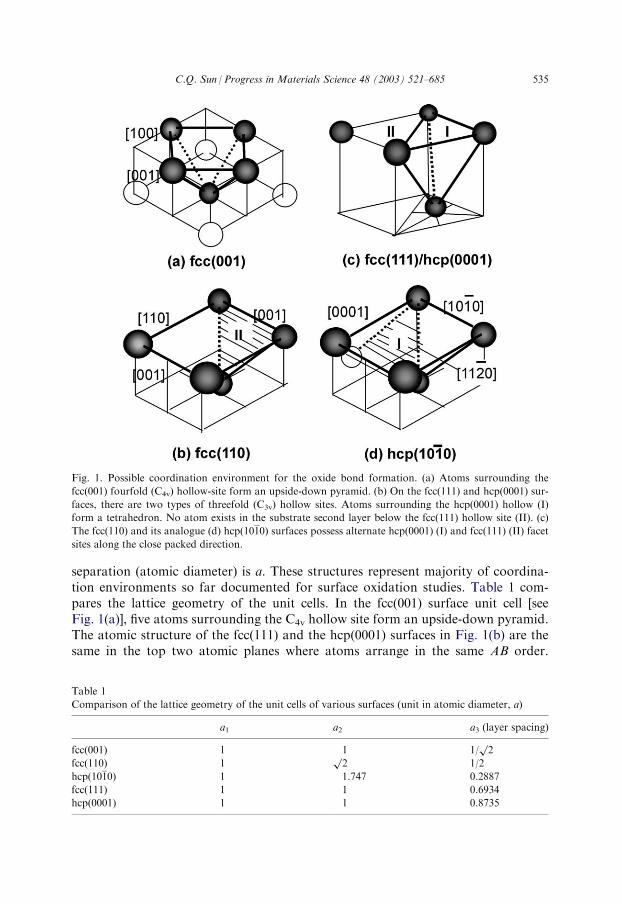
separation (atomic diameter) is a. These structures represent majority of coordina-tion environments so far documented for surface oxidation studies. Table 1 com-pares the lattice geometry of the unit cells. In the fcc(001) surface unit cell [seeFig. 1(a)], five atoms surrounding the C4v hollow site form an upside-down pyramid.The atomic structure of the fcc(111) and the hcp(0001) surfaces in Fig. 1(b) are thesame in the top two atomic planes where atoms arrange in the same AB order.
Fig. 1. Possible coordination environment for the oxide bond formation. (a) Atoms surrounding the
fcc(001) fourfold (C4v) hollow-site form an upside-down pyramid. (b) On the fcc(111) and hcp(0001) sur-
faces, there are two types of threefold (C3v) hollow sites. Atoms surrounding the hcp(0001) hollow (I)
form a tetrahedron. No atom exists in the substrate second layer below the fcc(111) hollow site (II). (c)
The fcc(110) and its analogue (d) hcp(1010) surfaces possess alternate hcp(0001) (I) and fcc(111) (II) facet
sites along the close packed direction.
Table 1
Comparison of the lattice geometry of the unit cells of various surfaces (unit in atomic diameter, a)
a1
a2 a3 (layer spacing)fcc(001)
1 1p1/p2
fcc(110)
1 2 1/2hcp(1010)
1 1.747 0.2887fcc(111)
1 1 0.6934hcp(0001)
1 1 0.8735C.Q. Sun / Progress in Materials Science 48 (2003) 521–685 535

Atoms surrounding the hcp(0001) hollow (indicated I) site form a tetrahedron whileatoms surround the fcc(111) hollow (indicated II) site cannot because there is noatom in the second layer. Atoms surrounding the fcc(110) and the hcp(101
-0) hollow
sites [in Fig. 1(c and d)], form a rectangular-pyramid of C2v symmetry. Besides thelong-bridge hollow site, there are two facet sites along the close packed direction inthe fcc(110) and the hcp(101
-0) surfaces. One is the hcp(0001) facet hollow site (I)
that involves one atom in the top layer and two atoms in the second layer; the otheris the fcc(111) facet (labeled II) that contains two atoms in the top layer and one inthe second layer along the close packed direction. The fcc{(110), (111)} surfaces areanalogous to the hcp{(101
-0), (0001)} surfaces with a slight difference in the inter-
atomic spacing.Table 2 lists the values of electronegativity (�), possible valencies and the atomic
radius of representative elements of different electronic structures. The difference inelectronegativity between atoms of two elements determines the nature of the bondbetween them. If the � is sufficiently high (around 2), the bond is ionic, otherwise it iscovalent or polar-covalent [102]. Normally, the atomic size of a noble (4d) metal isgreater than that of a transition (3d) metal and the electronegativity of the noblemetals is higher than that of transition metals. It is noted that an atomic radius isnot a constant but varies with the coordination number of this atom. Importantly,atomic radii change with alteration of valencies. It will be shown that, these basicsplay important roles in specifying the site of the adsorbate and the orientation of thebasic oxide tetrahedron and hence the patterns of observations for the chemisorbedsurfaces.
2.1.2. Bonding effectsBond formation is a process in which valence electrons transport. This should
have enormous effects on the surroundings by polarization and mass transportation.Alteration of atomic sizes will change the atomic distances and modify the surfacemorphology. Besides the well known bonding states of metallic, covalent, ionic andVan der Waals bonds in nature, polar-covalent bonds, non-bonding lone pairs, anti-bonding dipoles, H-like bonds and hydrocarbon-like bonds also exist.
Table 2
Electronegativity, possible valencies and the CN-related atomic radius of typical elements after Gold-
schmidt [101] and Pauling [102]
Element C
N O S i Co C u A g R u R h P d VElectronic
structure
2
s2p2 2 s2p3 2 s2p4 3 s2p2 3d74s2 3 d104s1 4 d105s1 4 d75s1 4 d85s1 4 d105s0 3d34s2� 2
.5 3 .0 3 .5 1 .9 1.9 1 .9 1 .9 2 .2 2 .2 2 .2 1.6Rion (Valency) 2
.6 (�4) 1 .71 (�3) 1 .32 (�2) 0 .41 (4) 0.82 (2) 0 .53 (1) 1 .00 (1) – – – –Rm (CN=1) 0
.771 0 .70/0.74 0 .66/0.74 1 .173 1.157 1 .173 1 .339 1 .241 1 .252 1 .283 1.224Rm (CN=12) 0
.914 0 .88/0.92 - 1 .316 1.252 1 .276 1 .442 1 .336 1 .342 1 .373 1.338536 C.Q. Sun / Progress in Materials Science 48 (2003) 521–685
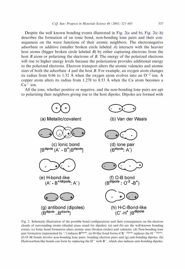
Despite the well known bonding events illustrated in Fig. 2(a and b), Fig. 2(c–h)describes the formation of an ionic bond, non-bonding lone pairs and their con-sequences on the wave functions of their atomic neighbors. The electronegativeadsorbate or additive (smaller broken circle labeled A) interacts with the heavierhost atoms (bigger broken circle labeled B) by either capturing electrons from thehost B atom or polarizing the electrons of B. The energy of the polarized electronswill rise to higher energy levels because the polarization provides additional energyto the polarized electrons. Electron transport alters the atomic valencies and atomicsizes of both the adsorbate A and the host B. For example, an oxygen atom changesits radius from 0.66 to 1.32 A when the oxygen atom evolves into an O�2 ion. Acopper atom alters its radius from 1.278 to 0.53 A when the Cu atom becomes aCu+ ion.All the ions, whether positive or negative, and the non-bonding lone pairs are apt
to polarizing their neighbors giving rise to the host dipoles. Dipoles are formed with
Fig. 2. Schematic illustration of the possible bond configurations and their consequences on the electron
clouds of surrounding atoms (shaded areas stand for dipoles). (a) and (b) are the well-known bonding
events. (c) Ionic bond formation alters atomic sizes (broken circles) and valencies. (d) Non-bonding lone
pair formation (represented by ‘:’) induces Bdipole. (e) H-like bond forms if B+/dipole replaces the H+/dipole.
(f) O–M bonds involve non-bonding lone pairs, bonding electron pairs and (g) anti-bonding dipoles. (h)
Hydrocarbon-like bonds can form by replacing the H+ with B+, which also induces anti-bonding dipoles.
C.Q. Sun / Progress in Materials Science 48 (2003) 521–685 537

expansion of atomic sizes and elevation of the DOS in energy space. The productionof the dipoles and the dipole–dipole interaction in the opposite direction will raisethe system energy. It is therefore reasonable to term such an event as anti-bondingdipole formation—an extreme case of the Van der Waals bond interaction. Anti-bonding is a by-product of reaction and it never forms between atoms of differentelectronegativity [108].Non-bonding lone pairs form when a pair of electrons of a specific atom occupies
a directional bonding orbital. This happens to electronegative elements in the upper-right part of the periodic table, such as nitrogen, oxygen and fluorine when the 2s,2px, 2py 2pz orbitals of these elements are hybridised [103]. It is often the case thatpart of the hybridized orbitals are occupied by shared electron pair (bonding)between A and B and the remaining orbitals by the lone electron pairs (non-bond-ing) of the electronegative additives. The number of lone pairs of an adsorbate fol-lows a ‘4� n’ rule and the n is the valence value of the adsorbate. For oxygen (n=2),two lone pairs are present while for nitrogen (n=3) only one lone pair forms duringthe sp-orbital hybridization. The ‘4� n’ rule holds for any elements in which the sporbitals hybridize. The lone pair requires an interaction with a B atom throughpolarization without any charge transport. The lone pair is actually not a bond butthe weaker part of the hydrogen bond.The classical hydrogen bond (O�2–H+/dipole : O�2), known for over 50 years, plays
an essential role in the structure and function of biological molecules. The ‘–’ and ‘:’represent the bond and the lone pair, respectively. Hydrogen bonds are responsiblefor the strength and elasticity of materials, such as wood or a spider’s web, mole-cular binding, as well as base pairing and folding in DNA. Hydrogen bonds are alsoresponsible for the synthesis and transferring of protein signaling [104,105]. It is tobe noted that the formation of the hydrogen bond is not due to the existence ofatoms of hydrogen or oxygen but due to the existence of the non-bonding lone pairs.If the lone-pair-induced Bdipole bonds further to an electronegative element A, thenan H-like bond (O�2–B+/dipole :O�2) forms. H-like bonding differs from the classicalhydrogen bond simply in that, the B+/dipole replaces the H+/dipole in the hydrogenbond (see Fig. 2e). If an atom of another electronegative element, such as C, replacesone of the oxygen ions then the (C-4–B+/dipole : O�2) configuration forms, which wasspecified in some cases as the anti-hydrogen bond [106]. This is also a H-like bond.Formation of such a H-like bond depends merely on the existence of the lone pairrather than the particular elements involved. Hence, the H-like bond is more gen-erally applicable though it is not often referred to as such. The same is true for thehydrocarbon-like bonds. The hydrocarbon bond is polar covalent in nature. Thenaked H+ also polarizes and attracts electrons of its neighboring atoms. Hydro-carbon-like bond can form by replacing the H+ with B+. The B+ is less electro-negative than the carbon.Unfortunately, the production of nonbonding lone pairs, anti-bonding dipoles,
H-like bonds and the hydrocarbon-like bonds are often overlooked. However, theseevents indeed play crucial roles in determining the physical properties of a systemthat involves electronegative additives. Quite often, a system contains several kindsof chemical bonds, such as in graphite and in an oxide. Because of the sp2-orbital
538 C.Q. Sun / Progress in Materials Science 48 (2003) 521–685

hybridization of carbon, the Van der Waals bond dominates in the [0001] directionwhile the stronger covalent bond dominates in the (0001) plane of the graphite. Ascan be seen from Fig. 2(f and g), O–B bond formation involves sharing pairs ofelectrons (bond), non-bonding lone pairs and anti-bonding dipoles. The electronicenvironment surrounding an oxygen atom varies from site to site at the subatomicscale.From an energy point of view, bond formation lowers the system energy and sta-
bilizes the system. Anti-bond (dipole) formation requires additional energy.Although it is energetically less favorable, the anti-bond can still form as a by-pro-duct of the events of bonding and non-bonding. Occupation of the orbitals by non-bonding electron lone pairs of an electronegative element, in principle, neither raisesnor lowers the system energy with respect to the energy level of the isolated atoms ofthe electronegative element [107,108]. From the band structure point of view, theanti-bond derived DOS (or polaron) should locate at energy above EF or near to itdue to the energy rise of the polarized electrons. The DOS features for bonding arelocated below the originally occupied levels of the electronegative element; while theDOS features of non-bonding lone pairs are located between that of the bond andthat of the anti-bond. Hydrogen-like bond formation will stabilize the system aselectrons transport from the high-energy anti-bonding states to the lower bondingstates. Bond and anti-bond formation will produce holes below the EF of the hostmaterial [93], which should be responsible for the transition from metal to semi-conductor when a compound forms.
2.2. Chemical bond: the basic tetrahedron
The original idea of the model is to extend the H2O molecular structure to a solidsurface with chemisorbed oxygen by replacing the H atom with a host atom of anarbitrary element B, as illustrated in Fig. 3(a). Two factors are taken into account inthe modeling considerations. First, the atomic radius is not constant but varies withchanges in not only its atomic valency, but also, its CN. Second, the sp orbitals ofoxygen hybridize and a quasi-tetrahedron forms. The bond angles and the bondlengths are not constant but vary within limits. Therefore, an oxygen atom can reactwith atoms, in any gaseous, liquid or solid states of an arbitrary element B throughtwo bonding electron pairs and two non-bonding lone pairs.Besides the well-known fact that an atom changes its radius when its valency
alternates, both the ionic and metallic radii of an atom contract with reducing theCN of this atom. Goldschmidt [101] suggested that, if an atom changes its CN from12 to 8, 6 and 4, then the ionic radius would be reduced by 3, 4 and 12% corre-spondingly. Pauling [102] also noted that the metallic radius contracts considerablywith reduction of theCN of the metal atom (see examples in Table 2). One may extendthe CN-imperfection induced radius contraction to atoms at a solid surface or sitessurrounding defects (such as point defects and stacking errors) though no such attempthas been reported previously. It is understandable that the surface provides an idealenvironment for CN reduction. Termination of the lattice periodicity in the surfacenormal direction reduces the CN of an atom at the surface. Such a CN-reduction
C.Q. Sun / Progress in Materials Science 48 (2003) 521–685 539

shortens the remaining bonds of the surface atom. It is reasonable to consider theCN-effect on the atomic radius as a Goldschmidt-contraction for an ionic bond or aPauling-contraction for a metallic. There exists sufficient evidence for the bondcontraction at metal surfaces [65–72]. For instance, about a 10% reduction of thefirst layer spacing of the (Ru [109], Co [110] and Re [111])(101
-0) surface has been
detected using LEED measurements and DFT calculations. The interlayer distancebetween the first and second layer of the diamond (111) surface is �30% smallerthan the interlayer separation in the bulk, which leads to a substantial reduction ofthe surface energy [112]. However, it has been reported that the dimer bond lengthsfor the IIA (Be and Mg(0001) surface) and IIB (Zn, Cd, and Hg) elements are longerthan the corresponding nearest neighbor atomic separation of the bulk values [72],which is conflicting with Pauling’s premise [102]. Table 3 summarizes the surfaceinterlayer relaxations of some metals caused by the Pauling-contraction.Oxygen interacts with atoms of element B [Fig. 3(a)] and hybridizes its sp orbitals
to form four directional orbitals. Oxygen captures two electrons from B atoms andthe 2s and 2p levels of oxygen are fully occupied with eight electrons that will repo-pulate in the four directional orbitals. Therefore, two of the four hybridized orbitalsare occupied by shared electron pairs (bonding orbitals). The remaining two orbitalsare occupied by the lone electron pairs of oxygen (non-bonding orbitals). It may benecessary to point out that the sp orbitals of oxygen hybridize independently with-out the involvement of orbitals of atoms of other elements, but the hybrid orbitalsmay be occupied by electrons of the others. Therefore, the orbital to be occupied isone thing; the actual occupancy of the hybridized orbital is another. The orbital can
Fig. 3. (a) The primary oxide quasi-tetrahedron and (b) the corresponding DOS features of bonding, non-
bonding, anti-bonding and holes [94]. Each of the two ions, 1 and 2, donates one electron to the central
oxygen to form the Goldschmidt-contraction ionic bonds. Atoms labeled 3 are the lone-pair-induced
metal dipoles with expansion of sizes and elevation of energy states. Arrows represent the process of
charge transportation. The arrow from the anti-bonding sub-band to the bond states corresponds to the
process of H-like bond formation.
540 C.Q. Sun / Progress in Materials Science 48 (2003) 521–685

be occupied by any kind of electron pairs (sharing or non-sharing). In a bondingorbital, the extent of electron sharing, or the nature of the bond, depends on thedifference in electronegativity (�) between the oxygen and element B. Due to thehigh � value (see Table 2), oxygen catches an electron from B (labeled 1 and 2) toform the Goldschmidt-contraction ionic bond at the surface. Formation of the non-bonding lone pairs, however, is independent of the nature of element B. The lonepairs are likely to polarize atom B (labeled 3) and the B atom becomes a Bdipole withassociated expansion of size and elevation of energy of the polarized electrons thatoccupy the anti-bonding energy levels.In an oxide tetrahedron, the plane (3O3) composed of the lone pairs and the
oxygen nucleus should be ideally perpendicular to the plane (1O2) that consists ofthe two bonding orbitals. The distance (1–2) between the two B+ ions and the spa-cing (3–3) between the Bdipole and Bdipole match closely the first and second shortestatomic spacing at a surface, which involves two atomic layers. The Bdipole tends tolocate at the open end of a surface due to the strong repulsion between the dipoles.The B2O primary tetrahedron is not a standard one but it is distorted due to thefollowing two effects: (i) The difference in repulsion between the occupied orbitalsvaries the bond angles [BAij (angle ffiOj), i, j=1, 2, 3 correspond to the atoms aslabeled; BA124104.5�, BA33 >109.5�] and, (ii) the difference in CN of atoms atdifferent sites adjusts the bond length [BLi=(RM++RO�2 )�(1-Qi), i=1, 2; Qi arethe effective bond contracting factors]. The length of BL3 and the angle BA33 mayvary with the coordination circumstances in a real system.It is unavoidable that the oxide tetrahedron formation dislocates the B atoms
collectively in the otherwise regular lattice sites. Moreover, oxygen always seeks fourneighbors to form a stable quasi tetrahedron. On the other hand, the expansion ofatomic radius and the energy rise of the dipole electrons are responsible for theprotrusions in the STM images and the reduction of the local work function. The
Table 3
Summary of the observed surface interlayer relaxation of clean metal surfaces. Origin for the conflicting
relaxation of the Be(0001) surfaces is yet not clear [72]
Metal
Method �d12/d12 Metal Method �d12/d12 (%)Rh(001)
LEED [113,114] �1.2;�1.4 Fe(210) LEED [115] �22W(001)
DFT [116] �5.7 Fe(310) LEED [115] �16W(110)
LEED [114,117] �3.0 Pd(310) DFT [71] �14.1W(320)
DFT [118] �22.3 Pt(210) LEED/EAM [119] �23.0/�31;Al(001)
DFT [68] �10 Cu(331) DFT [125,120] RSGF [121] �22.0;�13.8;�10.4Al(210)
LEED [122] �16 Cu(551) RSGFa [121] �9.8Ti/Zr(0001)
DFT [72,123]LEED [114]
�6.1��7.8
-4.9
Cu(211)
DFT [124,125,121]LEED [126]
�14.4;�28.4;-10.8
�14.9
Ag/Cu/Ni
(110)[127,128] �6��9 Cu(117) LEED [129] DFT [130] �13.0;-9.5Ag/Cu/Ni
(111), LEED �1��2 [131] Al(113) DFT [132] �6.8Ag/Cu/Ni
(100) [67] �2��3 Al(115) DFT [132] �8.0Fe/W(110)
DFT [393,133] �10.0;�13.0 Al(117) DFT [132] �8.3Be(0001)
LEED [134] +5.8 Al(331) LEED [135] �11.7a RSGF: Real-space Green’s function method. d12 is the separation between the top two atomic layers.
C.Q. Sun / Progress in Materials Science 48 (2003) 521–685 541

localized dipole electrons are also responsible for the non-Ohmic rectification at thesurface, even though the local work function reduces significantly. The strong loca-lization of dipole electrons at the surface increases the surface contact resistancebecause these electrons cannot move easily. The consequences of dipole formation inthis model agree with Lang’s theory [136–138] that an oxygen adsorbate affects theSTM current predominantly by polarizing metal electrons, as a result of anti-bond-ing dipole formation.At the initial stage of oxidation, the oxygen molecule dissociates and the oxygen
atom interacts with the host atoms through a single bond. It will be shown later(Section 3) that the O�1 occupies a specific position where the O�1 bonds directly toone of its neighbors and polarizes the rest. For the transition metals, such as Cu andCo, of lower electronegativity (� <2) and smaller atomic radius (<1.3 A), oxygenoften bonds to an atom at the surface first. For noble metals, such as Ru and Rh, ofhigher electronegativity (�>2) and larger atomic radius (>1.3 A), oxygen tends tosink into the hollow site and bonds to the atom underneath first. The ordering ofbond formation leads to different patterns of reconstruction. The O�1 also polarizesother neighbors and pushes the Bdipole at the surface radially outward from theadsorbate. Because of oxide tetrahedron formation with lone pair non-bonding anddipole anti-bonding, the electronic structure surrounding a certain atom varies fromsite to site.
2.3. Valence density-of-state (DOS)
The formation of bonds, non-bonding lone pairs and anti-bonding dipoles as wellas the H-like bonds generates corresponding features adding to the DOS of thevalence band and above of the host, as illustrated in Fig. 3(b). Arrows represent thekinetic processes of electron transportation. Initially, energy states below the EF of ametal are fully occupied in the ideal case at T=0. The work function, �0, Fermienergy, EF, and the vacuum level, E0, follow the simple relation: E0=�0+EF. ForCu, as an example, E0=12.04 eV, �0=5.0 eV and EF=7.04 eV. The Cu-3d bandlocates at energies range over from �2.0 to �5.0 eV below EF. The oxygen 2p statesare around �5.5 eV with respect to EF for Cu. At the initial stage of reaction, anelectron from a metal is transported from its outermost shell to the unoccupied 2porbital of the oxygen, which produces a hole in the outermost shell of the metal. TheO�1 polarizes its rest neighbors to form a polaron, as a result. This simple processcreates additional DOS features of bonding (<<EF), holes (4EF) and anti-bondingdipoles (4EF).With the full occupancy of the p-orbital of oxygen, the sp orbitals of the O�2
hybridize, which brings about four additional DOS features, as illustrated inFig. 3(b):
� Electronic vacancies are produced right below EF, generating a gap betweenthe conduction band and the valence band of a metal. The electron trans-portation can also expand the original band-gap of a semiconductor fromEG0 to EG1.
542 C.Q. Sun / Progress in Materials Science 48 (2003) 521–685

� The non-bonding (lone pair) states of O�2 locate below EF without apparentenergy change, in principle, compared to the 2p-level of an isolated atom ofoxygen [107].
� The bonding states are close to the originally occupied 2p-level of the isolatedoxygen.
� The anti-bonding (lone-pair-induced dipole) states are located above EF ornear to it. The oxygen-induced dipole reduces the work function from �0 to�1.
� Upon being overdosed with oxygen, H-like bonds form at the surface. Theoverdosed oxygen gets electrons from the dipoles and the Bdipole becomesB+/dipole. Thearrow fromthe anti-bonding states aboveEF to the deeperbondingsub-band represents the process of H-like bond formation. Apparently, thisprocess lowers the system energy.
It is noted that the hole-production and the lone-pair production are independent butsimultaneous, which result in the joint DOS features below EF. If the products of bothprocesses are compatible in quantity, the joint DOS features derived by the two pro-cesses may not be easily separated. The hole-production is due to two mechanisms:bonding and anti-bonding. For the Cu example, the 4s electrons (in the conductionband, CB) either contribute to oxygen for the bonding or jump up to the outer empty-shell (Cu 4p for example) for the anti-bonding dipole. Such bonding and anti-bonding processes empty the states just below EF, which result in the Cu-oxide beinga semiconductor with a known band-gap ranging from 1.2 to 1.5 eV [139,140].STS and VLEED revealed that the states of anti-bonding of the O–Cu system range
over 1.3�0.5 eV above the EF and the non-bonding states �2.1�0.7 eV below.Angular-resolved inverse PES [141] detected that the features of empty states at +2.0eV decrease with increasing oxygen coverage on the Cu(110) surface. The PEEM stud-ies of O–Pt surfaces [79,142–144] have detected the conversion of the dark islands, inthe scale of 102 mm, into very bright ones with work functions �1.2 eV lower than thatof the clean Pt surface. As will be shown in Section 4, the bonding states are around�5.5 eV below EF which is shifted slightly towards an energy lower than the 2p-levelof the oxygen because the hybrid bond forming lowers the system energy. Moststrikingly, all the oxygen-derived DOS features are strongly localized in real space.
2.4. Surface potential barrier (SPB)
2.4.1. One-dimensional SPB modelThe SPB experienced by electrons traversing the surface region contains two parts
[145]:
V r; Eð Þ ¼ ReV rð Þ þ iImVðr; EÞ ¼ ReV rð Þ þ iIm VðrÞ � VðEÞ½ � ð2:4:1Þ
The real part, ReV(r), describes the elastic scattering of the incident electronbeam. Integration of the ReV(r) along the moving path of the electron beam deter-mines the phase-shift of the electron beam.
C.Q. Sun / Progress in Materials Science 48 (2003) 521–685 543

It is adequate to consider the surface normal direction and the Re(r) will beReV(z) which has the form [146]:
ReVðzÞ ¼f�V0= 1þ Aexp½�Bðz � z0Þ�� �
; z5 z0 ða pseudo-Fermi-z functionÞ
1-exp l z � z0ð Þ½ �� �
= 4 z � z0ð Þ½ �; z < z0 ðthe classical image potentialÞ
ð2:4:2Þ
where A and B are constants given by B=V0/A and A=�1+4V0/l. The z-axisis directed into the crystal. V0 is the muffin-tin inner potential constant of thecrystal and z0 is the origin of the image plane. l describes the degree ofsaturation.The imaginary part, ImV(r), describes the spatial decay of the incident beams.
ImV(E) represents the joint effects of all the dissipative processes including excita-tion of phonons, photons and single-electron as well as plasmon excitation. Plasmonexcitation occurs at energy much higher than EF (normally �15 eV above EF). Atvery low energy, plasmon excitation does not come into play. Excitation of phononand photon requires energy smaller than the work function. Single-electron excita-tion occurs at any beam-energy that is greater than the work function and in thespace occupied by electrons. The spatial distribution of electrons is described by �(r)(charge density) which relates to the inelastic damping potential, ImV(r). Spatialintegration of the ImV(r, E) determines the amplitude-loss of the scattered electronwaves. An ImV(z, E) can be defined to include the effects that damping occurs in theelectron-occupied space (Fermi z decay) and that damping takes place at incidentbeam energy being greater than the work function, which depends on the occupiedDOS [88]:
ImVðz;EÞ ¼ Im½VðzÞ � VðEÞ�
ImVðE; zÞ ¼ � �ðzÞ � exp E � �L Eð Þ½ �=½ �
¼ � expE � �LðEÞ
� �= 1þ exp �
z � z1ðz0Þ
�ðz0Þ
� �� � ð2:4:3Þ
and,
�Lðx; yÞ ¼ E0 � EF; and EF / n ð2:4:4Þ
where and are constants depending on the calibration of the measuredspectral intensities. The terms z1(z0) (�(z1)=0.5�bulk) and �(z0) (saturationdegree) involved in the Fermi z function describe the spatial distribution ofelectrons contributing to the damping of incident beams. The spatial integrationof �(z) from a position inside the crystal to infinitely far away from the surfacegives the local DOS (n(x, y)). Therefore, �L(E) can extend to cover situationsthat are E dependent and to large surface areas over which the LEED methodintegrates.
544 C.Q. Sun / Progress in Materials Science 48 (2003) 521–685

2.4.2. 3-D effect with DOS contributionThe ReV(r) correlates with the ImV(r) through the Poisson equation [147]:
r2½ReVðrÞ� ¼ ��ðrÞ; and; ImVðrÞ / �ðrÞ: ð2:4:5Þ
The gradient of the ReV(r) relates to the intensity of the electric field "(r):![ReV(r)]=�"(r). If �(r)=0, then the ReV(r) corresponds to a conservative field inwhich the moving electrons will suffer no energy loss and the spatial variation of theinelastic potential ImV(r) / �(r)=0. It is to be noted that the ReV(z) transforms atz=z0 from the pseudo-Fermi z function to the 1/(z�z0) dominated classical imagepotential. Therefore,
r2½ReVðz0Þ� ¼ ��ðz0Þ ¼ 0: ð2:4:6Þ
The origin of the image-plane, z0, acts as the boundary of the surface regionoccupied by electrons. If we permit z0 to vary with the surface coordinates, then thez0(x, y) provides a contour of the spatial electron distribution, which should besimilar to that plotted using STM imaging method. The SPB features are thuscharacterized by the z0 and this effect allows us to choose z0 as the parameter in thesingle-variable parameterization of the nonuniform-SPB [88].In order to correlate the parameters that used to be treated as independent, and to
ensure the uniqueness of solutions, we define the SPB parameters as functionaldependents of z0. They are supposed to be correlated with z0 through a Gaussian-type function:
z1 z0ð Þ ¼ z0 � exp � z0 � z0Mð Þ= 1� 2n o
; ð2:4:7Þ
�ðz0Þ ¼ 1=l z0ð Þ � expn��z0 � z0mð Þ= 2
2o;
l z0ð Þ ¼ l0Mnx þ ð1� xÞ � exp
���z0 � z0Mð Þ=lz
2�o; ðx ¼ 0:4732Þ
Constants 1 and 2 are the full width at half maximum (FWHM) of the Gaussianfunctions and optimized to be 0.75 and 1.50, respectively [148]. The minimum z0m isestimated to be �1.75 Bohr radii. The l0M=1.275 is the maximum of l corre-sponding to maximum z0M=�3.425 Bohr radii and to lz=0.8965 for theO–Cu(001) surface. These constants may vary with materials considered.
2.4.3. Physical indicationsEqs. (2.4.2–2.4.4) represent not only correlation among the SPB parameters but
also correlate to STM profiles. At the dipole site, z1M�z0M, ��l�1, while in theatomic vacancy or ion positions, z1m<<z0m due to the strong localization ofelectrons at the surface. The ImV(z) is much less saturated than is the ReV(z) inthe site giving STM depressions. The SPB increases its degree of saturation with the
C.Q. Sun / Progress in Materials Science 48 (2003) 521–685 545

outward-shift of the image plane z0. This means that formation of metal dipolesshifts the electron clouds outward and enhances the density of the shifted clouds.Except for the inner potential constant V0, all the SPB parameters l, � and z1
become functional dependents of z0. The number of SPB variables is thus reducedfrom four to one. In addition, decoding VLEED using the correlation producesresults of clearer physical indication.More importantly, the electronic structure described with the SPB ties in closely
with the valencies and positions of atoms at the surface. In order to reflect the inter-dependence of the SPB and bond geometry, we have developed a decoding techniqueused for the particular O–Cu(001) surfaces [98,99]. In calculations, the VLEED codereads in the SPB constants and the atomic positions that were converted from thebond geometry. The code then automatically optimizes the z0 towards a duplicationof the measured intensity at each point of energy. Besides the bond geometry and theSPB constants, the calculation duplicates the spectrum and produces a z0(E) profile ofwhich the shape varies with the atomic structure employed. The z0(E) profile showsjoint features of surface morphology and the valence DOS as VLEED integrates overlarge (mm level) areas of surface. One can judge an optimal atomic geometry by ana-lyzing the shape of the z0(E) profile against physical constraints [98]. A combinationof the parameterized SPB and the z0-scanning calculation method reconciles the bondgeometry (atomic positions), surface morphology [ReV(z) and ImV(z)] and the DOSchange [z0(E) and ImV(E)] as a coherent system. This original approach may reflectthe real process of reaction because electrons are tied in closely with the positions andvalencies of surface atoms, and the reaction is a kinetic process in which atoms movecollectively. Typical results will be shown in Section 3.2.3.
2.5. Summary
We may end up the modeling section with a brief summary. The H2O moleculestructure and the concept of CN-imperfection induced atomic radius contractionhave been extended to the oxidation of a solid surface. This leads to the currentmodel for oxide-tetrahedron bond formation and its effects on the valence density-of-states and the surface potential barrier, as well as their interdependence:
� Oxygen can interact with atoms of an arbitrary element B to form a tetra-hedron with bonding and non-bonding states, as well as anti-bonding dipolesdue to polarization.
� Oxygen derives four additional DOS features that add to the valence bandand above of the host. These features of bonding, non-bonding, anti-bondingand electron holes are strongly localized.
� Oxygen induces the non-uniformity of the SPB. All the SPB parameters arecorrelated to the image plane (z0) which corresponds to the boundary of thesurface region occupied by electrons.
� The bond geometry, atomic valency, valence DOS and the SPB are inter-dependent. One may need to pay equal attention to these categories in dealingwith the surface chemisorption.
546 C.Q. Sun / Progress in Materials Science 48 (2003) 521–685

� Some important yet often-overlooked events, such as non-bonding lone pairs,anti-bonding dipoles and the H-like bond are crucial in practice.
In the next section, we report our exercises of applying the original BBB model toresults drawn from a database of surface oxidation. It will be shown that the sig-natures of STM/S, LEED, PES and TDS as well as the EELS and Raman can beexplained in terms of atomic valencies, bond geometry, valence DOS and bondstrength as well as bond forming kinetics. Formation of the oxide tetrahedron andthe valence DOS and the bond forming kinetics are found to provide common baseto explain all the systems analyzed.
3. STM and LEED: atomic valencies and bond geometry
3.1. Phase ordering
Table 4 summarizes the phase orderings occurred at the low-index O–(Cu,Rh){(001), (110), (111)} surfaces and their analogues of O–(Co, Ru){(101
-0), (0001)}
surfaces. The O–Pd(110) surface performs in the same way as the O–Rh(110) surface.It will be shown later that the O–(V, Ag)(100) surfaces perform differently from theO–(Cu, Rh)(001) surfaces despite the same geometrical configuration. Incorporatingthe primary bond model to these phase structures, we can derive the formulae of
Table 4
Oxygen induced phase ordering on the typical metal surfaces. The hcp(0001) and hcp(1010) faces are
analogues to the fcc(111) and fcc(110) faces, respectively. Please refer to Fig. 1 for the lattice geometry
Cu(fcc)
Rh(fcc) Co(hcp) Ru(hcp)fcc(001)
c(2�2)-2O�1 off-centered pyramidp p
c(2�2)-2O�1 radial
and inverse pyramid
( 2�2 2)R45�
-2O�2 missing row
c(2�2)p4g-2O�2 or
c(4p2�4
p2)-16O�2
Refs.
[21,36,38,81,94,97,149–155]
[52,156,–167]
fcc(110) or
hcp(1010)
Disordered
(1�1)-O�1 (hollow)
Disordered
(2�1)-2O�1 (atop)
(2�1)-O�2 (Ni,
Ag, Pt)
c(2�2n)p2mg-nO�2
(n=2,3,4) (Pd)
c(2�4)-4O�2
c(2�4)-4O�2c(6�2)-8O�2
(2�1)p2mg-2O�2 (2�1)p2mg-2O�2Refs.
[2,16,21,34,35,9,47,48,3,74,94,168–170]
[17–182]
[42,43,183,184,109,185]
[110,168,187]
fcc(111) or
hcp(0001)
radial (2�2)-O�1
(hcp-hollow)
radial (2�2)-O�1
(hcp-hollow)
‘29’ & ‘44’
structures
c(2�2)-2O�2
pairing row
c(2�2)-2O�2
pairing row
(1�1)-O�2
(1�1)-O�2Refs.
[188,49] [52,53,54,189–194] [55,56,257,85,189,195–200]
C.Q. Sun / Progress in Materials Science 48 (2003) 521–685 547

reaction at various stages, which enables the atomic valencies in the first two atomiclayers to be specified. As will be discussed in detail subsequently, the phase transi-tion originates from nothing more than the alteration of the oxygen valency (asassigned in Table 4) under a certain geometrical configuration at different oxygencoverage. In the following sections, we will analyze these well-determined repre-sentatives from the perspective of bond forming.
3.2. O–Cu{(001), (110), (111)}
3.2.1. Observations
3.2.1.1. O–Cu(001). Since 1956 when Young et al. [1] found that the Cu(001)surface is more easily oxidized than other faces of the copper single crystal, therehave been many conflicting opinions regarding the oxygen-induced Cu(001) surfacereconstruction. Different atomic superstructures have been derived with variousexperimental techniques [201] and theoretical approaches [33,202]. The missing-row(MR) type Cu(001)-(
p2�2
p2)R45�-2O reconstruction, first proposed by Zeng and
Mitchell in 1988 [149,150], has been elegantly accepted. The latest conclusion[19,38,94,15] about the phase forming kinetics was that a short-ordered nanometricCu(001)-c(2�2)-O�1 precursor phase forms at 25 L (Langmuir=10�6 torr.sec) oxy-gen exposure or lower, and then the ordered MR (
p2�2
p2)R45�-2O�2 structure
follows (the valencies of oxygen are denoted based on the current model for readers’convenience).It was resolved from the STM images in Fig. 4 that oxygen prefers the next-near-
est-neighboring hollow site throughout the course of reaction. This implies thestrong site-specificity of the oxygen adsorbate [151,203]. At the initial stage of reac-tion (Fig. 4a), nanometric c(2�2)-2O�1 domains dominate with zigzag and U-typeprotruding boundaries. Upon increasing oxygen exposure, the short ordered c(2�2)-O�1 phase evolves into the ordered (
p2�2
p2)R45�-2O�2 structure by every fourth
row of Cu atoms becoming missing. In the second phase, the ‘dumb-bell’ shapedprotrusions in Fig. 4b bridge over the missing rows. The ‘dumb-bell’ protrusionswas interpreted as [36]: ‘the pairing of Cu–O–Cu chains by displacing the Cu and/orO atoms next to the missing row by about 0.35 A towards the missing row’ and ‘theO-Cu-O chain is formed by the delocalized anti-bonding states’. The separation ofthe paired rows was estimated to be 2.9�0.3 A. The length of the bright spot wasabout 5.1 A. The height of the bright spot was 0.45 A compared to the 0.3 A pro-trusions on the pure Cu(001) surface [36].Clearly, as can be resolved from the STM images for the precursor, the atomic
valencies of the Cu atoms sitting inside the domain of ‘depression’ differ completelyfrom that of the Cu atoms composing the protruding boundaries. The atomicvalencies of the paired protrusions should also differ from the depressions in thesecond phase. This was the starting point that triggered the original exercise toidentifying the atomic valencies at the surface. We may note that obtaining a high-quality STM image is infrequent and the form of the image is often subject to the tipconditions and the applied bias voltages [204,205]. For instance, an asymmetrical tip
548 C.Q. Sun / Progress in Materials Science 48 (2003) 521–685
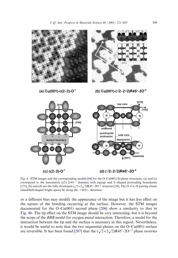
or a different bias may modify the appearance of the image but it has less effect onthe nature of the bonding occurring at the surface. However, the STM imagesdocumented for the O–Cu(001) second phase [206] show a similarity to that inFig. 4b. The tip effect on the STM image should be very interesting, but it is beyondthe scope of the BBB model for oxygen-metal interaction. Therefore, a model for theinteraction between the tip and the surface is necessary in this regard. Nevertheless,it would be useful to note that the two sequential phases on the O–Cu(001) surfaceare reversible. It has been found [207] that the (
p2�2
p2)R45�-2O�2 phase reverses
Fig. 4. STM images and the corresponding models [94] for the O–Cu(001) bi-phase structures. (a) and (c)
correspond to the nanometric c(2�2)-O�1 domains with zigzag- and U-shaped protruding boundaries
[151]; (b) and (d) are the fully developed (p2�2
p2)R45�-2O�2 structure [36]. The O–Cu–O pairing chains
(dumbbell-shaped bright spots) lie along the <010> direction.
C.Q. Sun / Progress in Materials Science 48 (2003) 521–685 549

into the initial precursor state after sputtering by an energetic Ar+ beam and followedby flashing the sample up to 520 K. When annealing the (
p2�2
p2)R45�-2O�2 sur-
face at a temperature corresponding to the ‘dull-red’ color of the Cu surface for halfan hour [208], sp-orbital de-hybridization occurs to the oxygen [209]. The atomicgeometry of the O–Cu(001) surface has been intensively studied using various tech-niques. The divergence of opinions is summarized in Table 5.
3.2.1.2. O–Cu(110). The O–Cu(110) surface has also been investigated inten-sively ever since the pioneer LEED study reported by Ertl in 1967 [2]. LEIS [210,211]and SEXAFS [169,212,213] studies suggest a missing-row type reconstruction whereevery other [010] Cu row on the surface is absent. In comparison, HEIS [214] andSTM [47,215] investigations support a buckled-row (BR) model in which the everyother row of Cu atoms is not missing but is shifted outwards instead. Moreover,XRD [57], LEED [216] and ICISS [217,218] measurements indicate an added-row(AR) type reconstruction. STM imaging [219–221] could finally settle the disagree-ment in favor of the missing-row reconstruction, which, however, should be viewedas an ‘added-row’ phase due to the mass transportation mechanism. The MR andAR models were thought to be the same at the saturation coverage, although themass transport for these two models is different [222]. The MR model requiresremoval of alternate [010] Cu rows while the AR model requires addition of alter-nate [010] Cu rows by Cu-surface diffusion. Step edges presumably serve as sinks orsources for Cu atoms at lower oxygen coverage. However, discrepancies exist on theheight of the oxygen atom and on the extent of the interlayer relaxation between thetwo topmost Cu layers.A summary of the structural parameters pertaining to the O–Cu(110) surface is
given in Table 6. It shows clearly that the results vary considerably depending on thedata sources. XRD [74] gives a considerably large first-layer expansion D12=1.65 A
Table 5
Structural discrepancies for O-Cu(001) surface (Unit in A)a
Ref. M
ethod D Cux D Ox D Oz D Cuz D 12 B ond length[81] V
LEED �0.8 1 .90 c (2�2)0.3
0.0 �0.2 �0.1 1 .90[38 S
EXAFS 0.25 0.03 0.2 0.1 1 .86 2.07�0.15��0 3
�0.1 0.8 0 –0.25 c (2�2)[206] S
TM, LEED 0.3 0.0 0.1 0.1 1 .94 1 .91[150] L
EED 0.3 0.0 0.1 0.1 1 .94 1 .81, 2.04 1.84(2)[154] L
EED, PED, NEXAFS 0.1�0.2 0 �0.25 0.25 0.1�0.2 2 .05 1 .94[152] L
EED 0.10 0.0 0.10 �0.05 2 .06[3] E
MT >0.0 < 0.0 0.3�0.5[36] S
TM �0.35 �0.35[93,97] V
LEED B ond length: 1.63(1); 1.77(1); 1.94 (2) A, ionic bond angle: 102.5, lonepair angle: 140.0
a All are missing row structures unless otherwise denoted c(2�2). Parameters are the first interlayer
spacing, D12, the shift of the atom near the missing row (DCux, DCuz) and the displacement of the
adsorbate (DOx, DOz).
550 C.Q. Sun / Progress in Materials Science 48 (2003) 521–685

(+30%) and a second-layer contraction D23=1.15 A (�11%), and the oxygen islocated, DO=0.34 A, beneath the missing-row layer. In contrast, a theoretical opti-mization [9] suggested a smaller first layer-expansion D12=1.331 A (+4%) withoxygen located �0.5 A above the top layer. For the clean Cu(110) surface,D12=1.17 A (�8.5%) and D23=1.307 A (+2%) [66,170], as compared to the bulk-interlayer distance Dbulk=1.278 A. The lateral displacements (parallel to the sur-face) of the Cu atoms remain very small. The measured vertical position of theoxygen is quite uncertain and it varies considerably from positions above to belowthe expanded first-layer of Cu atoms. An average of the reported values is oftenused.Pouthier et al. [223] examined the reported data and found a strong correlation
between the values of DO and D12. By taking parameters for charge transfer [223],and the surface potential barrier [89,93] into account, numerical solutions would bemore complex. As can be seen from Fig. 5, the overall trend of the correlationbetween D0 and D12 can be accounted for by a simple linear expression [88]:
DO ¼ �1:982�D12 þ 2:973� 0:136 A�
:
The coefficients have no apparent physical meanings. The correlation between DO
and D12 has generated numerous mathematical solutions that have caused long-lasting arguments.Nevertheless, all the numerical solutions covered by the correlation region (Fig. 5)
could be correct from a numerical point of view. This should be true as the diffrac-tion intensity depends on the arrangement of the scattering centers with variousdiffraction cross-sections. The cross-section of diffraction should vary with theeffective number of electrons of the scattering atom. The arrangement of scatteringcenters determines the phase-shift of the diffracted beams. The cross-section of thescatter determines the amplitude of the diffracted waves. Therefore, the diffraction
Table 6
The geometrical details of the Cu(110)-(2�1)-O surface (unit in A)a
D12
D23 D DO DCu(1)-O DCu(2)-OICISS [170]
1.60�0.13 1.15�0.06ICISS [210]
1.51�0.04 �0.10�0.10 1.81�0.01 1.90�0.10ICISS [217,218]
1.51�0.04 1.28�0.20 0.12�0.07 �0.08�0.15 1.81�0.01 2.00�0.14LEED [216]
1.49�0.03 1.21�0.03 0.03�0.03 0.04�0.03 1.81�0.01 2.01�0.05SEXAFS [213]
�0.35 1.82�0.02 1.99�0.02SEXAFS [283]
�1.31 �0.2 1.84�0.02 2.00�0.05XRD [48]
1.65�0.05 1.28�0.01 0.031�0.005 �0.34�0.17 1.84�0.06 1.85�0.16Theory [8]
�1.331 �0.48Theory [23]
1.60�0.05 �0.21�0.1Model [93] +data [48]
1.655 0.031�0.005 �0.60 1.675 1.92Theory [293]
1.877�0.2 �0.1�0.2a Listed are layer spacing D of the corresponding layers, the lateral shift of the second-layer atoms
towards the missing first-layer rows, the vertical O position DO relates to the first layer, and the bond
length to the nearest and the next-nearest Cu neighbors of the O adsorbate [21].
C.Q. Sun / Progress in Materials Science 48 (2003) 521–685 551

can identify nothing about the nature of the scattering centers but only show theresultant effect of scattering from the geometrical arrangement of the scatteringcenters of different cross-sections. With XRD and DFT, Vlieg et al. [224] determinedfor the Cu(410)–O surface two detailed structural solutions which give equallyacceptable fits to the XRD data after imposition of a Leonard–Jones penalty factor.These models differ especially in the O positions, but one is found to be morefavored by comparison with the results of the DFT calculations, and by considera-tions based on bond lengths and valence.It can be found from Fig. 5 that the vertical position of the adsorbate ranges from
DO=�0.01�0.59 A relative to the buckled Cu layer. The spacing between the sec-ond and the top Cu layer D12 is 1.50�0.16 A. If the top Cu layer buckles upward,the adsorbate will buckle inward, and vice versa. For each pair of values of (D12,DO) that fit the diffraction data there must exist a counterpart set that also fit. Forexample, the value at point [8] couples with the value at point [10]. Both are thenumerical solutions for the same system. This couple can be obtained by rotating theO–Cu–O chain 180� around its axis, and followed by offsetting the O–Cu–O chain inthe vertical direction. A half lattice-constant glide shift along the O–Cu–O chain isalso necessary. The exchange in the vertical position of O and Cu (0.59/0.16=3.68)seems to approach the ratio of atomic numbers ZCu/ZO=58/16=3.63. This relationinfers indeed, to a certain extent, that the cross-section depends on the charge of thespecific scattering center. Therefore, all the solutions along the line from [8] to [10]can find a counterpart that could fit the diffraction data. The vertical change of
Fig. 5. Correlation between the interlayer spacing D12 and the oxygen position DO with respect to the
topmost Cu plane (see inset) [88]. The data are given in Table 6. The symmetry points for O and Cu are
0.01�0.59 and 1.50�0.16 A. Case [8] transforms to [10] can be realized by rotating the O–Cu–O chain
around its axis 180� and shifting the axis from 1.166 (O above) to 1.540 A (O below). This indicates the
uncertainty of atomic positions derived from diffraction.
552 C.Q. Sun / Progress in Materials Science 48 (2003) 521–685

positions for both the partners should satisfy the numerical relation between D0 andD12. However, the simple operation on the O–Cu–O chain provides entirely differentphysical meanings. Therefore, physical constraints should be necessary for the mul-tiple solutions. For instance, the on-surface oxygen should be excluded for the fullydeveloped surface oxidation. This is because the Cu+ and O-2 are hardly detectableusing an STM due to the altered atomic valencies. The on-surface oxygen shouldproduce no protrusions in the STM images. As will be discussed later, the verticalpositions of the sub-surface oxygen also give different geometrical configurations ofthe oxide tetrahedron.Considerable efforts with STM imaging have also been made on studies of the
O–Cu(110) surface [47,168,215,217,218,220]. A typical STM image and the corre-sponding model for the (2�1)-O phase are illustrated in Fig. 6. In the STM image,the round bright spots of 0.8�0.2 A in height are separated by 5.1 A in the [110]direction and 3.6 A in the [010] direction. Single O–Cu–O strings are formed alongthe [010] direction, or perpendicular to the close-packed Cu row. In contrast, theprotrusion for the clean Cu(110) surface is about 0.15 A [47].Exposing the Cu(110)-(2�1)-O�2 surface to higher amounts of oxygen at T>300
K initiates a second structural phase of c(6�2)-8O�2. STM images of the c(6�2)-8O�2 structure [48,168,225,226] show a corrugation pattern consisting of a quasi-hexagonal arrangement of ‘ellipsoid’ protrusions. Fig. 7 shows the c(6�2) domainsadjacent to the (2�1) phase. Higher resolution images of the c(6�2) structure in theright-hand panel display additional weaker features between the large ‘bumps’. Theheight of the bright spots was reported to be 0.6�0.1 A, slightly lower than the
Fig. 6. STM image [47] and the corresponding models [93] for the surface atomic valencies of Cu(110)-
(2�1)-O�2 [219]. The STM grey-scale is 0.85 A, much higher than that of metallic Cu on a clean (110)
surface (0.15 A). The single ‘O�2 : Cudipole : O�2’ chain is zigzagged by the non-bonding lone pairs and
composed of the tetrahedron.
C.Q. Sun / Progress in Materials Science 48 (2003) 521–685 553

round spot in the (2�1)-O�2 surface, but much higher than that of the clean Cu(110)surface.Feidenhans’l et al. [48,226] derived a structural model based on their studies using
the combination of STM and XRD measurements and EMT computations. Themodel illustrates that, in the second phase of the O–Cu(110) surface, there are twokinds of oxygen atoms with different vertical positions; every third row of Cu atomsis missed and additional Cu atoms are buckled up, crossing over the missing rows(see Fig. 7). Liu et al. [227] and Dorenbos et al. [228] further confirmed this structureby using the tensor-LEED and LEISS (low energy ion scattering spectroscopy),respectively. The vertical positions of the atoms are listed in Table 7. In the model ofFig. 7, the sublayers (labeled 1 and 3) are composed of Cu and the layers 2 and 4 areoxygen. The atomic valencies in various layers will be specified in the next sectionbased on a reaction formula.
Fig. 7. STM image [48] and the corresponding models [93] for the surface atomic valencies of Cu(110)-
c(6�2)-8O�2 phase. The STM grey-scale is 0.66 A. The ‘O�2 : Cudipole : O�2’ chains are paired by the
rotation of every other tetrahedron that produce the dipole bridge over the missing row. The pairing
chains interlock the Cu+/dipole at the surface with regularly protruding dipoles.
554 C.Q. Sun / Progress in Materials Science 48 (2003) 521–685

3.2.1.3. O–Cu(111). It has been understood that the dissociate adsorption ofoxygen on the Cu(111) surface roughens the surface with short-range order [2,229].HREELS studies [230] suggest that oxygen chemisorbs at the threefold hollow site,either in, or below, the outermost plane of Cu atoms, resulting in a small work func-tion change. LEISS studies [231] revealed that oxygen induces a restructuring thatinvolves a 0.3 A displacement of Cu atoms. SEXAFS [232] determined that oxygenatoms adsorb in the threefold hollow sites with the O–Cu bond of 1.83�0.02 A inlength, close to the corresponding bulk value for Cu2O (also the average bond lengthdetermined in the current study). The Cu–Cu distance is considerably relaxed(3.15�0.1 A) with respect to the Cu-Cu separation in the bulk (2.555 A). Furthermore,an IPES study [233] revealed that an extra band around 3.0 eV is produced above EF at%, the center of the first Brillouin zone. These earlier observations provide strong evi-dence that the O–Cu(111) surface reconstructs with short-range order. The re-arrangement of the Cu atoms indicates that the impinging oxygen adsorbate ‘pushesout’ the Cu atoms that roughen the surface of the disordered oxide precursor [21].With a combination of STM, HEISS, and LEED, Jensen et al. [188] found two
new well-ordered, O-induced commensurate reconstructions with extremely largeunit cells, 29 and 44 times the (1�1) surface lattice, after an exposure of 300 L oxy-gen at 673 K and post-annealing to 723 and 773 K, respectively. Matsumoto et al.[234] confirmed these structural phases in a recent LEED and STM study. As shownin Fig. 8, there is a series of ‘double-holes’ and distorted ‘honey-comb’ frames com-posed of the ‘dumb-bell’ shaped bright spots as observed in the O–Cu(001) surface.
Table 7
Summary of the vertical positions of ion cores for the Cu(110)-c(6�2)-8O surface
D13
D23 D34STM, XRD, EMT [48,226], Tensor-LEED [227]
1.2 0.4 0.2LEIS [228]
0.45�0.12 0.40�0.12 0.12�0.12Fig. 8. (a) STM topography (It=2.9 nA, Vs=55 mV) of a 60�60 A2 region of O–Cu(111) surface show-
ing the ‘29’ structure. Grey scale is 0.27 A. (b) Topography (It=4.9 nA, Vs=7 mV) of a 60�60 A2 region
showing the ‘44’ structure. The grey-scale from black to white corresponds to 0.55 A [188].
C.Q. Sun / Progress in Materials Science 48 (2003) 521–685 555

3.2.2. AnalysisWe now turn to revisiting the well-determined O–Cu{(001), (110), (111)} surface
reconstructions from the perspective of bond forming. It is shown that the reactioncan be formulated by specifying the atomic valencies at the surfaces. The phaseordering and the derivatives originate from the formation of the O�1 and subse-quently the O�2 with sp-orbital hybridization. The various observations fromCu{(001), (110), (111)} surfaces with chemisorbed oxygen are purely the result ofgeometrical coordination effects on bond forming, because of the same atomic sizeand electronegativity.
3.2.2.1. Cu(001)-c(2�2)-2O�1: off-centered CuO2 pairing pyramid. Initially, theO2 molecule dissociates and then the oxygen atom immediately bonds to one atomat the surface. Bond theories [103,235] indicate that it is forbidden for an oxygenadsorbate to form identical bonds with four atoms which are located in the sameplane, because oxygen possesses at most four directional orbitals. The model inFig. 4c states that the O�1 forms a bond with one of its four neighbors at the surfaceand the O�1 polarizes the rest. This gives rise to two typical domains in a(p2�2
p2)R45� complex unit cell, which can be represented by:
O2 ðadsorbateÞ þ 7Cu ðsurfaceÞ
) 2O�1 þ Cuþ2�
ðdomainÞ þ 6Cudipole ðdomain boundaryÞ;
CuO2 pairing pyramidð Þ
or a (2p2�2
p2)R45� complex unit cell:
2 O2 ðadsorbateÞ þ 6Cu ðsurfaceÞ½ �
) 4 O�1 þ Cuþ1�
ðdomainÞ þ 8Cudipole ðdomain boundaryÞ
ð4CuO off-centered pyramidÞð3:2:1aÞ
The [2O�1+Cu+2] or the 4[O�1+Cu+1] domains form the depressed domains andthe O�1-induced Cudipole builds up the ‘engaged-cogwheels’ domain boundary thatare detected as U- or zigzag-shaped patches of protrusions in STM imaging (Fig. 4a).Larger domains consisting of c(2�2)-2O�1 unit cells can be constructed by addingmore oxygen adsorbates to the surface. The additional oxygen catches one electronfrom a dipole and polarizes its rest neighbors in the top layer. The model of thesurface matrix in Fig. 4c shows the alternative sign of charge distribution bothwithin the domains and in the domain boundaries. Therefore, the surface is fullycovered with dipoles in a way that stabilizes not only the domains but also the domainboundaries. At this phase, the surface stress should be tensile though further con-firmation is needed. Clearly, the atomic valencies of the copper atoms within thedomain (O�1, Cu+1 or Cu+2) differ from that at the domain boundary (Cudipole). It isto be noted that the surface reaction takes place without the second atomic layer beinginvolved at the precursor stage. There are no atoms missing in the short-ordered
556 C.Q. Sun / Progress in Materials Science 48 (2003) 521–685

c(2�2)-2O�1 surface. As optimized with VLEED, the small off-centered shift of theadsorbate (DOz �0.40 A. DOx �0.18 A is about 5% of the fourfold hollowdimension) is beyond the resolution of an STM.
Cu(001)-(p
2�2p
2)R45�-2O�2: Cu3O2 pairing tetrahedron. Upon increasingoxygen-exposure the ‘disordered’ nanometric Cu(001)-c(2�2)-2O�1 domain devel-ops into the ‘ordered’ (
p2�2
p2)R45�-2O�2 phase in which every fourth row of Cu
atoms is missing. As an intermediate and quasi-stable state, the O�1 tends to catchanother electron from its neighbors. Once its two bonding orbitals are fully occu-pied, the sp-orbital hybridization follows [97]. As a consequence, a tetrahedronforms with two additional orbitals that are occupied by lone electron pairs of theoxygen. The Cu(001) surface geometry allows the intriguing Cu3O2 pairing tetra-hedron to form in such a way that the substrate is involved, as shown in Fig. 4d. Aperspective view of the Cu3O2 pairing tetrahedron is illustrated in Fig. 9. We mayformulate the O–Cu(001) bi-phase ordering as the effect of the O�1 and subse-quently the hybridized-O�2 formation. The complete process of reaction is describedas follows:
Fig. 9. Perspective of the Cu3O2 pairing tetrahedron in the Cu(001)-(2p2�
p2)R45�-2O�2 unit cell [97]
[reaction formula is given in Eq. (3.2.1b)]. O�2 prefers the center of a quasi tetrahedron. Atoms 1 and 2
are Cu+2 and Cu+. Atom 3 is Cudipole and M is the vacancy of the missing Cu. Atom 4 is metallic Cu
atom. The pairing dipoles 3–3 cross over the missing row.
C.Q. Sun / Progress in Materials Science 48 (2003) 521–685 557

O2 ðadsorbateÞ þ 4Cu ðsurfaceÞ þ 2Cu ðsubstrateÞ
) 2O�1 þ Cu2þ ðsurfaceÞ - - - - - - - - - - - - - - - - ðCuO2 pairing pyramidsÞ
þ 3Cudipole ðO�1-inducedÞ þ 2CuðsubstrateÞ - - - - - - - - - - - ðbonding effectÞ
then, upon increasing oxygen exposure,
) 2O�2ðhybridÞ þ Cu2þðsurfaceÞ þ 2CuþðsubstrateÞ - - - - - - - - - - ðCu3O2
pairing tetrahedronÞ
þ 2Cudipole ðlone-pair inducedÞ þ Cu ðMR vacancyÞ - - - - - - ðbonding effectÞ
ð3:2:1bÞ
In the first phase, the Cu2+ connects the two off-centered pyramids on the surface toform a CuO2 (see lower side in Fig. 4c). In the second phase, the Cu
2+ couples twoCu2O-tetrahedra, giving rise to the Cu3O2 structure. The top layer of the Cu(001)-(p2�2
p2)R45�-2O�2 surface contains rows of Cu2+, a pairing [O�2 : Cudipole : O�2]
row and the missing-row vacancy; the second layer is composed of alternate rows ofCu and Cu+. In the second phase, the surface stress seems to be compressive due tothe repulsion among the surface dipoles. The adsorbate–adsorbate interaction isalways repulsive throughout the course of phase transformation because the identicalvalencies of them. It is pointed out that as the origin of the observations, the bondforming processes are hardly detectable with currently available means. What one isable to observe is the effect of bonding–dipole protrusions and missing row vacancies.
3.2.2.2. Cu(110)-(2�1)-O�2 : single O–Cu–O chain. Comparatively, the Cu(110)-(2�1)-O-2 surface reaction, as shown in Fig. 6, can also be expressed as an effectof the hybridized-O�2 formation. The characteristics of this phase is thecombination of the alternate missing-row (MR) of Cu and the buckled row (BR)of the ‘O�2 : Cudipole : O�2’ chain. The ‘:’ represents the lone electron pair of oxygenthat zigzags the buckled string.The formula for the MR+BR reconstruction is given as (for a c(2�2) unit cell):
O2 ðadsorbateÞ þ 4 Cu ðsurfaceÞ þ 4 Cu ðsubstrateÞ
) 2 O�2 ðhybridÞ þ 2Cuþ ðsubstrateÞ�
- - - - - - - - - - - - - ðCu2O bondingÞ
þ 2 Cu ðMR vacancyÞ þ Cudipole ðBRÞ�
- - - - - - - - - - - ðthe bonding effectÞ
ð3:2:2aÞ
or even the added row (AR) model:
O2 ðadsorbateÞ þ 4Cu ðsurfaceÞ þ 2Cu ðterrace edgesÞ
) 2 O�2 ðhybridÞ þ 2CuþðsurfaceÞ�
- - - - - - - - - - - - - - - ðCu2O bondingÞ
þ 2Cudipole ðbuckled ARÞ - - - - - - - - - - - - - - - - - - - - ðthe bonding effectÞ
ð3:2:2bÞ
558 C.Q. Sun / Progress in Materials Science 48 (2003) 521–685

om the mass-transport point of view, the Cu(110)-(2�1)-O�2 phase is made
Frsimply by every other Cu-row missing or an O–Cu–O raw being added which isbuckled up. Although the mass-transport mechanisms [222] in the MR+BR and theAR models are different, as reflected in the formulae, the cause of the reconstruction(Cu2O bonding) is the same.Formulae (3.2.2) indicate that all the MR, BR and the AR models are correct inthe sense of bonding effect, but the combination with their cause (Cu2O bondforming), would be complete. The model can also be applied to the similarfcc(110)-c(n�1)-O�2 surface of Ni, Ag [21], Pt [236] and Cu(112) surface, as well asthe bcc(112) surface of Mo and Fe with chemisorbed oxygen. Recently, Schroeder etal. [237] and Santra et al. [238] noted that the O–Mo(112) surface shares similarSTM patterns to that of the O–Cu(110) surface. Tan et al. [239] have found withSTM and LEED similar one-dimensional Cu–O–Cu strings added on the Cu(112)surfaces upon oxygen chemisorption. LEED study [240] revealed a missing-row typereconstruction forms at the Fe(112)-p(2�1)-O phase where the O–M–O chain runsperpendicular to the close-packed rows of the substrate.From the bond forming point of view, the bi-phase and related phenomena on the
O–Cu{(001), (110)} surfaces can be originated from charge transportation, that is, theO�1 and the hybridized-O�2 formation. Oxygen catches electrons one by one from itstwo nearest neighbors. As the effect of hybridized-O�2 on both the Cu(001) and theCu(110) surfaces, the lone-pair-induced dipoles are responsible for the protrusions inthe STM images. It is clear that the [: O�2 : Cudipole : O�2 :] chain is ‘zigzagged’ by thelone pairs (Fig. 6) rather than it is co-lined by states of anti-bonding, covalent bondingor even ionic bonding. The removal of the missing-row atom from both surfacesresults from the isolation of the specific Cu atom as its neighbors have already bondedto the oxygen. The Cu(110)-(2�1)-O�2 phase, whether added-row or missing-row,differs in origin from the Cu(001)-(
p2�2
p2)R45�-2O�2 surface by nothing more than
that the [O�2 : Cudipole : O�2 :] chain rotates around its axis by�45� to fit itself to thecoordination surroundings. The simple rotation has indeed yielded different valenciesof atoms in the surface planes. The difference in the coordination geometry betweenthe two surfaces appears to be the origin of the complexity of surface oxidation.Instead of an intermediate-O�1 state like that on the Cu(001) surface, O�2 forms
directly at the Cu(110) surface. The oxygen adsorbate may catch two electrons fromits nearest neighbors (shortest spacing, 2.552 A) in sequence. Meanwhile, the adsor-bate also requires extra atoms for the Cudipole to complete the tetrahedron. Due to theexpansion of dipole dimension and the repulsion between the non-bonding lone pairs,dipoles tend to expose to the open end of the surface. Apparently, oxygen atoms canhardly find edge atoms from a perfectly finished Cu(110) surface. The situation maychange, however, if the (110) face has sufficient terrace defects. This is suggested tobe the origin as to why the Cu(001) face is oxidized easier or harder. We maytherefore infer that the tetrahedron is the basic and stable building block in oxida-tion. If the tetrahedron is destroyed, oxygen will seek new partners for a new tetra-hedron—a process of re-bonding or bond switching. This may provide a mechanismfor O-penetrating in bulk oxidation and O-floating in the epitaxial growth of metalson the oxygen pre-covered metal surfaces [241,242].
C.Q. Sun / Progress in Materials Science 48 (2003) 521–685 559

We may also suggest a formula for the Cu(110)-c(6�2)-8O�2 phase with specifi-cation of the atomic valencies in different sublayers (Fig. 6d):
4O2 þ 12Cu ðsurfaceÞ þ 12Cu ðsubstrateÞ
) 4Cu ðMR vacancyÞ þ 2Cudipole ðsupplied by the MRÞ - - - - - - - ðlayer 1Þ
þ 4O�2 ðhybrid; large filled circleÞ - - - - - - - - - - - - - - - - - - - - - - ðlayer 2Þ
þ 8Cuþ=dipole ðserve as Cuþ for the upper O�2Þ - - - - - - - - - - - - - - ðlayer 3Þ
þ 4O�2 ðhybridÞ - - - - - - - - - - - - - - - - - - - - - - - - - - - - - - - - - ðlayer 4Þ
þ 4Cudipole ðinteracting with the upper O�2Þ - - - - - - - - - - - - - - - - ðlayer 5Þ
þ 8Cuþ ðsmall open circleÞ - - - - - - - - - - - - - - - - - - - - - - - - - - - ðlayer 6Þ
ð3:2:3Þ
Instead of varying the valencies of the oxygen adsorbate, further exposure atraised temperature increases the oxygen-coverage from 1/2 to 2/3 ML. Theprocess of oxygen re-bonding, which reorganizes the tetrahedron and the Cuatoms at the surface, changes the structural pattern. Self-organization of theCu2O tetrahedron yields two kinds of oxygen positions (layer 2 and 4), as canbe seen from the side view of Fig. 7. The lower O�2, the Cu+ at layer 6 andthe Cudipole at layer 3 build up the first Cu2O tetrahedron, which orientates thesame as the Cu2O in the (2�1)-O�2 phase. Acting as a donor for furtherbonding, the Cudipole at layer 3 provides an electron to the upper O�2 and theCudipole becomes Cu+/dipole. The non-bonding lone pairs of the upper O�2 theninduce the Cudipole at layer 1 and 5 to form another Cu2O tetrahedron with alteredorientation, which interlocks the O–Cu–O chains near to the missing row. Differingfrom the (2�1)-O�2, the substrate (sublayer 5 and 6) is composed of Cu+ andCudipole alternatively along the original O–Cu–O chain. They are arranged in a muchmore complicated array than even that of the second layer of the Cu(001)-(p2�2
p2)R45�-2O�2 phase. It is to be noted that two of the four missing Cu atoms
become the Cudipole that bridge over the missing row and they are responsible for therecorded STM ‘ellipsoid’ protrusions. The atomic arrangement specified by the tet-rahedron agrees with that determined by other researchers (refer to Table 7). Oneoxygen adsorbate atom locates below the Cu layer labeled 3 and the other oxygenabove. The possible mechanism causing such a more complicated phase is suggestedto be that thermal energy relaxes the Cu2O bonding and further exposure enhancesthe self-organization. The reversibility of the bond forming and a suitable ambientproduces a phase with more close-packed Cu2O and H-like bond involvement,which is even stable. Fig. 7 also shows the molecule structure of the pairing O–Cu–Ochain bridges over the missing row. The protruding dipoles are responsible for the‘ellipsoid’ STM protrusions.It is worth mentioning that the lone-pair-induced Cudipole (layer 3) interacts fur-
ther with the upper O�2. Such a set of interactions (O�2 : Cu+/dipole-O�2) forms anidentical system to the hydrogen bond by definition. Such configuration has been
560 C.Q. Sun / Progress in Materials Science 48 (2003) 521–685

defined as an H-like bond to discriminate the Cu+/dipole from the H+/dipole inthe hydrogen bond. According to the bond theory of Atkins [107], one mayfurther infer that the H-like bond forms if the lone-pair-induced dipole com-bines further with other electronegative specimen through bonding orbitals.Otherwise, an anti-bonding dipole is retained. It is known that the major con-tribution to an anti-bonding state is made by the less electronegative element[107]. Therefore, anti-bonding dipole-dipole interaction hardly ever formsbetween specimens with large differences in electronegativity. A typical exampleof the anti-bonding configuration is the quadruples in Fig. 4d, or the ‘dumb-bell’protrusions in the Cu(001)-(
p2�2
p2)R45�-2O�2 STM image. This inference
may be necessary in understanding the heterogeneous catalysis. For example,the formation of H-like bonds may provide a more feasible mechanism for formingisocyanate (N, C, O) on the Ru(0001) surface. As found by Kostov et al. [203],the isocyanate could only be formed on the Ru(0001) surface in the presence ofpre-adsorbed oxygen. It is expected that the anti-bonding electrons of the dipolesreadily combine with new adsorbates (nitrogen or carbon), lowering the systemenergy.
3.2.2.3. O–Cu(111). Reconstruction phases on the Cu(111)-O surface are mostcomplicated and the corresponding reaction formulae need to be defined. The Cu–Cu lattice distortion (3.15�0.10 A being the scale of dipole-dipole separation) isindicative of oxide tetrahedron formation. The STM protrusions (Fig. 8) and theoxygen-derived DOS (�3.0 eV) above the EF imply the presence of anti-bondingdipoles in the Cu(111)-O surface.
3.2.3. Quantification: bond geometry and bonding kinetics3.2.3.1. Kinetic VLEED from O–Cu(001). It is known that energetic electron
beams in LEED (E5102 eV) interact with a stack of ordered layers of ion cores.Information derived from LEED patterns is the symmetry and size of the unit cells.Decoding LEED I–V profiles generates knowledge about atomic positions but theaccuracy is always under question. In the VLEED (LEED with E<30 eV, or lowerthan the plasma excitation energy), electron beams interact with the valence elec-trons of a few surface atomic layers and with the potential barrier of the surface.VLEED provides highly informative data but sophisticated data processing isrequired. It has been shown that VLEED (at E<16 eV) could simultaneously collectnon-destructive information from the top layer of a surface about the behavior ofatoms (bond geometry) and valence electrons (DOS features) and the morphology(SPB) of the surface [99].Intensive calculations have been carried out on VLEED from an O–Cu(001)
surface [208,243]. The calculations used the code developed by Thurgate [81].The code involves multiple-diffraction events and multi-atoms in a complexCu(001)-(
p2�2
p2)R45�-2O�2 unit cell. Fig. 9 gives the Cu3O2 structure used in the
calculations. First, the calculation code reads in the parameters of the first interlayerspacing, D12, the shift of the Cu
dipole (DCux, DCuz) and the displacement ofthe adsorbate (DOx, DOz). These data are converted from variables of bond
C.Q. Sun / Progress in Materials Science 48 (2003) 521–685 561

geometry. The bond variables vary within a range that is subject to physicalconstraints. The bonds contract by Q1=0.12, Q2=0.04�0.04, the Cu
dipole shiftswithin DCux=0.25�0.25 A, and the bond angle BA12 varies within 104.5
�. Sec-ondly, the VLEED code optimizes the SPB constants such as the inner potentialconstant, V0, the amplitude of the inelastic potential, g, and the slope of theenergy dependence, d, of the imaginary part of the SPB (Section 2.4). Calcula-tions are performed based on the parameterized SPB by varying z0 over-2.5�1.25[for pure Cu(001)] in steps of 0.25 (atomic unit). A contour plot of z0 versus E isthen drawn with a matching between the calculated intensity and the measure-ment, Ic(z0i, E)/Im(E)=1.0�0.05. The z0(E) contour plot is the unique yield of thecalculation of this method. The plot shows the shape of the z0(E) curve that givesthe desired best fit of the measurement and shows all the possible solutions withinthe limits of parameter variation. This z0-scanning method is also a convenientway to compare different models and to refine the parameters of the SPB and thebond geometry.Once the refinement of the z0(E) plot is complete, the program automatically fits
the value of the z0(Ei) to give a desired level of agreement (for example 3% errorbar). In contrast to the z0-scanning method, the step of �z0 automatically variesfrom 0.25 to 0.0005 depending on the ratio of �=Ic(Ei)/Im(Ei). If � reaches therequired precision, calculation will automatically turn to the next energy step Ei+1
of measurement. This method yields simply the geometry-dependent z0(E) profileand reproduces the measured VLEED spectrum. Quantities such as the bond geo-metry, work function, barrier shapes and energy band structure are automaticallygiven as the product of the data processing.Decoding of the angular-resolved VLEED profiles from the O–Cu(001) surface
has yielded static information about the Brillouin zones, band structure and bondgeometry [244,245]. Calculations also reveal the non-uniformity and anisotropy ofthe SPB, and the distribution of the DOS in the upper part of the valence band. Ithas been revealed that oxygen adsorption has reduced the inner potential constant(V0) by 9.6% (from 11.56 a.u. to 10.5 a.u) and the work function by 1.2 eV from 5.0to 3.8 eV. The oxygen-reduced V0 is due to the transport of atoms and valenceelectrons at the surface. The lowered work function arises from surface dipole for-mation that increases the local charge density.VLEED revealed that, apart from long-term aging, the reaction upon aging and
annealing differs only slightly from that upon increasing the exposure of theO–Cu(001) surface. It was discovered from the decoding that annealing at a tem-perature of ‘dull red’ supplies energy for oxygen de-hybridization rather than thedriving force that enhances bond formation. Calculations excluded both the off-centered pyramid structure with oxygen higher than 0.4 A above the top layer andthe centered pyramid structure with four identical O–Cu bonds for the precursorc(2�2)-O�1 phase [209]. More details about the VLEED quantification of theO–Cu(001) bonding kinetics have been reported in Ref. [99]. For comprehensive-ness, here we introduce briefly the results that are of immediate relevance.Fig. 10(a–c) shows the VLEED (00) beam reflectance I00/I0 versus the incident
beam energy measured at 70� incidence and 42� azimuth angles [208]. It is obvious
562 C.Q. Sun / Progress in Materials Science 48 (2003) 521–685

that the VLEED spectral features are very sensitive to the oxygen-exposure. Thevariations of the typical peaks at 7.1, 9.1 and 10.3 eV show that the reaction pro-gresses in four discrete stages:
� YO 430 L: When the exposures are smaller than 30 L, the peak at 7.1 eVdecreases in magnitude until oxygen exposure reaches 30 L, while other peaksshow little change.
Fig. 10. Exposure-resolved VLEED spectra (a–c) measured at 70.0� incidence and 42.0� azimuth from the
O–Cu(001) surface [208], and the calculated results (d–f) from varying the individual bond variables of Q2,
BA12 and DCux. Variations of intensities in panel (a–c) at 7.1, 9.1 and 10.3 eV show four reaction stages.
Calculations (d–f) for 400 L oxygen-exposure by using bond variables can reproduce the trends of
measurement at different stages [97].
C.Q. Sun / Progress in Materials Science 48 (2003) 521–685 563

� 30 L<YO 435 L: In the region of 30–35 L, the decreased peak intensity at7.1 eV recovers a little.
� 35 L<YO4200 L: From 35 to 200 L, the first peak attenuates while one newpeak at 9.1 eV emerges; and then both the peak at 9.1 eV and the peak at 10.3eV have increasing to maximum values up to 200 L.
� YO > 200 L: When the exposures are greater than 200 L, a generalattenuation of the entire spectrum occurs.
The calculations for the 400 L oxygen-exposure by individually varying the bondvariables BA12, Q2 and BL2 can reproduce the measured trends, as summarized inFig. 10(d–f). Results indicate that:
� The oxygen-coverage is maintained at 0.5 ML throughout the course ofreaction.
� The results, especially, in panels (e) and (f), agree remarkably well with themeasured trends given in panels (b) and (c), respectively. This indicates thatthe process of Cu2O bond forming dominates in the reaction while the SPB isrelatively insensitive to the oxygen exposures.
� The four discrete stages of reaction can be simply simulated by varying thebondvariables individually.For instance, features appearing in the range from35to200Laredominatedby either the increaseof ff1O2orBL2extension.However,ff1O2 expansion and BL2 contraction is physically reasonable process. Thespectral features for samples with oxygen exposure greater than 200 L resultfrom the increase of DCux alone. From 30 to 35 L, the recovery of the peakat 7.1 eV can be realized by increasing the Q2 with smaller ff1O2 and smallerDCux.
� Variation of DCuz gives a little change of the spectral intensity between 9.5and 11.5 eV. Varying the DCuz produces no features that could matchmeasurements. Therefore, the individual shift of an atom at a time does notoccur in the real process of bond formation.
Fig. 11 shows the offset of the oxygen-exposure resolved z0(E) profiles, whichreproduce the measured spectra in Fig. 10(a–c). It is seen that the z0(E) profiles, ingeneral, are relatively insensitive to the variation of the exposure. The z0(E) profilesare similar in shape except for the slight difference below 7.5 eV for 25 L exposure.This further confirms the assumption that the SPB is much less sensitive to theexposure than the bond geometry. The slight outward-shift (-z direction, relative to�2.5 a.u. as indicated by broken lines) of the z0(E) curves at higher exposuresincreases the n(E), which reduces the work function in the area over which VLEEDintegrates (mm level). The shape of the z0(E) profile is a joint contribution of theoccupied DOS, n(E), and the surface corrugation (local spatial DOS n(x, y)). Thenon-constant form of the z0(E) can be understood as due to the O-induced ‘ratherlocal’ properties as revealed by STM and due to the non-uniform DOS in thevalence band as well. The �z0(E) in the z-direction is about (�2.3)–(�3.3) (atomicunit)=0.53 A which coincides with the �0.45 A STM grey-scale [36]. The vacating,
564 C.Q. Sun / Progress in Materials Science 48 (2003) 521–685
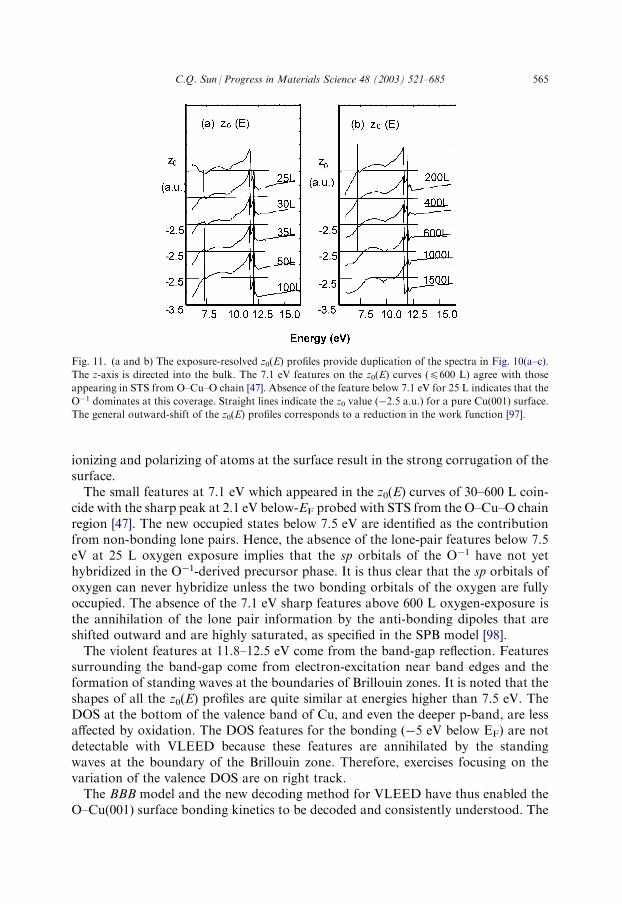
ionizing and polarizing of atoms at the surface result in the strong corrugation of thesurface.The small features at 7.1 eV which appeared in the z0(E) curves of 30–600 L coin-
cide with the sharp peak at 2.1 eV below-EF probed with STS from the O–Cu–O chainregion [47]. The new occupied states below 7.5 eV are identified as the contributionfrom non-bonding lone pairs. Hence, the absence of the lone-pair features below 7.5eV at 25 L oxygen exposure implies that the sp orbitals of the O�1 have not yethybridized in the O�1-derived precursor phase. It is thus clear that the sp orbitals ofoxygen can never hybridize unless the two bonding orbitals of the oxygen are fullyoccupied. The absence of the 7.1 eV sharp features above 600 L oxygen-exposure isthe annihilation of the lone pair information by the anti-bonding dipoles that areshifted outward and are highly saturated, as specified in the SPB model [98].The violent features at 11.8–12.5 eV come from the band-gap reflection. Features
surrounding the band-gap come from electron-excitation near band edges and theformation of standing waves at the boundaries of Brillouin zones. It is noted that theshapes of all the z0(E) profiles are quite similar at energies higher than 7.5 eV. TheDOS at the bottom of the valence band of Cu, and even the deeper p-band, are lessaffected by oxidation. The DOS features for the bonding (�5 eV below EF) are notdetectable with VLEED because these features are annihilated by the standingwaves at the boundary of the Brillouin zone. Therefore, exercises focusing on thevariation of the valence DOS are on right track.The BBB model and the new decoding method for VLEED have thus enabled the
O–Cu(001) surface bonding kinetics to be decoded and consistently understood. The
Fig. 11. (a and b) The exposure-resolved z0(E) profiles provide duplication of the spectra in Fig. 10(a–c).
The z-axis is directed into the bulk. The 7.1 eV features on the z0(E) curves (4600 L) agree with thoseappearing in STS from O–Cu–O chain [47]. Absence of the feature below 7.1 eV for 25 L indicates that the
O�1 dominates at this coverage. Straight lines indicate the z0 value (�2.5 a.u.) for a pure Cu(001) surface.
The general outward-shift of the z0(E) profiles corresponds to a reduction in the work function [97].
C.Q. Sun / Progress in Materials Science 48 (2003) 521–685 565

four-stage Cu3O2 bond forming kinetics is quantified as follows (refer to Fig. 9 andTable 8, also a multimedia as supplementary information):
� YO 430 L: The dissociated oxygen atom forms one contracting (Q1=12%)ionic bondwith aCu atom (labeled 1) on the surface.Meanwhile,metallic bondsbreak up and themissing row forms. TheDCux reaches 0.15 A and ff1O2 reaches94.0�. TheO�1 locates above the surface and forms anoff-centered pyramidwithits surface dipole neighbors. The missing-row atom seems to be attracted by thepairing O�1 and repelled by the dipoles, and eventually evaporates.
� 30 L<YO 435 L: The O�1 forms the second contracting (increase Q2 from 0to 4%) ionic bond with a Cu atom (labeled 2) in the substrate second layer;the sp orbitals of the O�2 start to hybridize. The O�2 penetrates into the bulk;meanwhile, the angle ff1O2 expands from 94.0� to 98.0�.
� 35 L<YO4200 L: The angle ff1O2 increases from 98.0� to a saturation valueof 102.0�, which causes the first interlayer spacing D12 to expand by about10%, while other parameters have little change.
� YO > 200 L: The interaction between the O�2 and the lone-pair-inducedCudipole develops. Lone pairs push the Cudipole outward, and consequently,pairing dipoles form and bridge over the missing row. The DCux increasesfrom 0.15 to a maximum 0.45 A at 800 L and above.
Table 8
Four-stage O–Cu(001) surface bonding kinetics [97]a
Reaction
stage
1
3
(<30 L: BL1 formation); 2 (30�35 L: BL2 and ff1O2 change);
(35�200 L: ff1O2 expansion); 4 ( ff 200L: DCux increase)
Exposure (
L) 25 30 35 50 1 00 2 00 4 00 6 00 5 800Bond
geometry
(Q1=0.12)
Q
B
D
2
0 0 0.04 0.04A12
92.5 94.0 98.0 1 00.0 1 01.0 1 02.0Cux
0.125 0.150 0.250 0.355 0.450Atomic shift
(A)
�
�
DCuz
0.1460 0.1440 0.1268 0.0938 0.0844 0.0709 0.1495 0.2239 0.2849DOx
0.1814 0.1796 0.1802 0.1831 0.1852 0.1877D
Oz �0.0889 �0.0447 0.0618 0.1158 0.1422 0.1682Layer D
12 1.7522 1.7966 1.8287 1.8824 1.9086 1.9343Bond length
(A)
B
B
L1
1.628L2
1.850 1.776B
L3 1.8172 1.8326 1.8833 1.8983 1.9053 1.9121 1.9262 1.9396 1.9505Bond angle
(�)
B
B
A13
95.70 98.82 1 04.24 1 05.12 1 05.64 1 05.33 1 05.30 1 04.01 103.83A23
91.80 93.11 95.75 96.46 96.83 95.18 99.52 1 01.67 103.43B
A33 1 65.87 1 60.83 1 45.26 1 44.32 1 43.02 1 41.82 1 39.43 1 35.38 135.71a Empty space is identical in value to that in the corresponding cell of the previous column. All infor-
mation is provided by the controlling variables (BA12, Q2, DCux). Error bar for bond length is 0.010 A
and for bond angle is 0.2�. The SPB constants: V0=10.50 eV, =�0.9703, =6.4478.
566 C.Q. Sun / Progress in Materials Science 48 (2003) 521–685

Representing the joint spatial and energy DOS, the variations of the structural-dependent z0(E) profiles (Fig. 11) agree with the bonding kinetics:
� The slight outward-shift of the z0(E) profile at higher exposures reduces theworkfunction, which corresponds to the development of the anti-bonding Cudipole.
� Features below 7.5 eV, particularly the small sharp peak at 7.1 eV, arederivatives of the non-bonding lone pairs of the O�2. The absence of thesefeatures at 25 L originates from the O�1 precursor, in which no lone pair hasformed; while at higher oxygen exposures the lone pair information is anni-hilated by the protruding Cudipole characteristics.
� Similarity of the fine-structure shapes at energies higher than 7.5 eV of all theprofiles implies that electrons in the lower part of the valence band involve nomuch in the process of charge transportation. In contrast, electrons in theupper part of the valence band dominate in oxidation: holes and lone pairsform simultaneously. The DOS features of bonding (around 12 eV) are notdetectable with VLEED due to the standing wave formation in the bound-aries of Brillouin zones.
3.2.3.2. XRD from O–Cu(110). Feidenhans’l et al. [74] determined the atomicstructures of the O–Cu(110) surface using XRD. Their results agree with the trendpredicted by EMT optimisations for the minimized total binding energy of the sys-tem [3]. Both XRD and EMT approaches revealed that the oxygen adsorbates arelocated underneath the missing-row top layer and the zigzag O–Cu–O chains areformed (refer to Fig. 6). Referring to the inset in Fig. 5, the vertical displacement ofthe dipole (labeled 3) is denoted as D3z. The distance from oxygen to the buckled Cutop layer is DOz. The lateral displacement of the Cu
+ row in the second layer isD1x. The z-axis is directed into the bulk. Thus the bond parameters can be con-verted from these data [74]:
D1x; DOz; D3zð Þ ¼ ð0:031�0:005; 0:34�0:17; -0:37�0:05Þ A�
: ð3:2:4Þ
As can be seen from Table 9, a slight change of the DOz varies the bond geometry.The different values of bond lengths represent quite different meanings in thephysics. The value of DOz=0.34 A gives a tetrahedron with four O–Cu bondsthat are nearly identical in length (Column I). The value of BL3 41.85 Aimplies that the atom labelled 3 is an ionic one. The Cu+ ion is hardly detect-able by STM due to the partially emptied d-states and the reduced atomicradius (from 1.27 to 0.53 A). This is apparently conflicting with the STM ima-ges that show the Cu atom buckling out of the surface. Lowering the oxygenadsorbate within the error bar (0.17 A) to DOz=0.51 A gives results in ColumnII. BL1 has a 6.5% contraction and BL3 extends slightly compared with thestandard ionic bond length, 1.85 A. The bond geometry is now acceptable asthe shorter bond corresponds to the ionic state of the Cu. Structural parametersin column II are acceptable while those in column I are strictly forbidden in line
C.Q. Sun / Progress in Materials Science 48 (2003) 521–685 567

with physical constraints and STM observations. The ideally suggested case,assuming the CN of the O�2 and the Cu+ as 4 (Q=0.12) and 8 (Q=0.03), isshown in column III. By adopting the value D3z=0.37+0.05 A, one can theninsert into this frame a tetrahedron [BL1=BL2=1.32�(1�0.12)+0.53�(1�0.03)=1.675 A], in which the O�2 ion is located 0.6 A beneath the dipole layer. Thegeometry of this tetrahedron is nearly identical to that determined for theCu(001)-(
p2�2
p2)R45�-2O�2 phase. Although the patterns of reconstruction
and morphology are different, the basic tetrahedron is the same in both theCu(001)-O�2 and the Cu(110)-O�2 surfaces.
3.2.4. SummaryIn summary, we have obtained the quantitative information about the bond
geometries and bond forming kinetics on the O–Cu(001) and the O–Cu(110) sur-faces. VLEED calculations revealed that the Cu3O2 pairing-tetrahedron evolvesfrom the CuO2 pyramid on the Cu(001) surface [Fig. 4(c and d)]. Both thebond theories and the VLEED calculations suggest that, in the precursor phase,the O�1 locates eccentrically above the fourfold hollow-site of the c(2�2)-2O�1
domain to form an off-centered pyramid. The off-center shift of the O�1 isDOx�1.807�[1.85�(1�0.12)]�0.18 A, which is comparable to the values of 0.10–0.13 A, as reported previously [38,154]. The vertical distance of the O�1 to the sur-face is �0.4 A above the surface. The absence of the lone-pair DOS features impliesthat no sp-orbital hybridization occurs of oxygen in the O�1-induced precursorphase.Except for the Cu(001)-c(2�2)-2O�1, all the available phases on the O–Cu(001)
and the O–Cu(110) surfaces are composed of the primary Cu2O tetrahedron. Theparameters for the Cu2O tetrahedron are nearly the same, as summarized in Table 9.The VLEED gave quantitative data that the work function is reduced by �1.2 eVand the inner potential constant decreases from 11.56 eV for the clean Cu(001) sur-face to 10.50 eV upon being oxidized. The SPB parameters vary from site to site onthe surface [88]. At the dipole site, z1ffiz0, �ffi l�1. This means that the metal dipoles
Table 9
Comparison of the tetrahedron bond geometries derived from the XRD from Cu(110)-(2�1)-O�2 and the
VLEED from Cu(001)-(p2�2
p2)R45�-2O�2 [93]
Variable
Cu(110) (2�1)-O�2 (p2�2p2)R45�-2O�2
ConclusionI
II IIIDOz
40.34 0.51 0.60BL1 (A)
51.85 1.73 1.675 1.628 <1.85 BL2 (A) 51.85 1.73 1.675 1.776 <1.85BL3(2) (A)
41.84 1.88 1.921 1.926 �1.92BA12 (�)
490.0 96.0 102.5 102.0 <104.5BA33 (�)
5156.7 146.5 140.3 139.4 �140.0BA13/23 (�)
497.4 100.2 102.3 99.5/105.3 �102.5568 C.Q. Sun / Progress in Materials Science 48 (2003) 521–685

enhance the SPB through the outward shift of the wave function. Dipole formationalso strengthens the degree of saturation of both the real and the imaginary part ofthe SPB at the dipole site.The SPB of the Cu(001)�O�2 surface varies considerably from that of the clean
Cu(001) surface. The z0M at dipole site is (z0M/z0(Cu)=3.37/2.50�) 1.35 times andthe lM is (lM/l(Cu)=1.27/0.9�)
p2 times that of the pure Cu(001) surface. The
values of z0M and lM quantify the protrusions in the STM image to a certain extentas the higher the electronic islands are, the denser the electrons will be there. In themissing-row site, z1 <<z0, � >> l�1, i.e., the missing-row vacancy is not occupiedby ‘free electrons’ of the solid. This may quantify the depression in the STM ima-ging. On the Cu(001)–O�2 surface, the lowest saturation degree and the smallestz-scale of the SPB is (z0m/z(Cu)=1.75/2.5 ffi lm/l(Cu)=0.65/0.9�) 1/
p2 times that
of the clean Cu(001) surface. Therefore, electrons at the surfaces with chemisorbedoxygen are rather local. It is reasonable to describe metal surfaces with chemisorbedoxygen at higher coverage as a non-Fermi system. This is because of the lack of freelymoving electrons at the surface. This mechanism should cause the non-Ohmic rectify-ing and higher contact resistance even though the local work function is much lowerthan that of the clean Cu(001) surface. It is understandable now why a standard free-electron resistance mechanism could not work in such as strongly localized system [41].Decoding the exposure-resolved VLEED data from the Cu(001)–O�2 surface
revealed that three bond parameters dominate the four-stage bonding kinetics. Inthe process of oxidation, the oxygen adsorbate first forms one Goldschmidt-con-traction ionic bond (1-O) to a Cu atom on the surface, and then another contractingionic bond (2-O) follows between the oxygen and a Cu in the substrate. As a result,the oxygen adsorbate buckles into the bulk. Then, the ionic bond angle (ff1O2)increases, leading to the relaxation of layer spacing. Finally, interaction developsbetween the lone pairs of oxygen and the lone-pair-induced metal dipoles (3-O).During the process of oxidation the change of the SPB is not apparent except for theDOS features of the non-bonding lone pairs.From the perspective of bond forming, the origin of the bi-phase ordering on both
the O–Cu(001) and the O–Cu(110) surfaces has been clear. It is interpreted thatthe formation of O�1 and subsequently the hybridized-O�2 gives in nature theCu(001)-c(2�2)-2O�1 and then the Cu(001)-(
p2�2
p2)R45�-2O�2 phases. Re-
assembling of the primary Cu2O tetrahedron transforms the Cu(110)-(2�1)-O�2
into the Cu(110)-c(6�2)-8O�2 phase at elevated temperatures and higher expo-sures. As consequences of O-2-hybridization, the Cu(001)-(
p2�2
p2)R45�-2O�2
differs from the Cu(110)-(2�1)-O�2 in origin by nothing more than the fact that the[O�2 : Cudipole : O�2] string rotates itself by �45� to match the specific coordinationenvironment. Such a chain-operation yields entirely different reconstruction patternsand surface morphologies of the two surfaces. Therefore, the phase ordering on theCu(001)–O and the Cu(110)–O surface is simply the consequence of the Cu2O for-mation at different stages and under various bonding circumstances. The mechanismfor the O–Cu(111) surface reconstruction should be the same because the Cu{(001),(110), (111)} surfaces differ one from another by nothing more than the crystalorientation.
C.Q. Sun / Progress in Materials Science 48 (2003) 521–685 569

3.3. O–(Rh, Pd)(110)
3.3.1. ObservationsIt has been clear that oxygen adsorbate occupies the long-bridge hollow-site on
the fcc(110) surfaces of Cu, Ni, Ag, and Pt to form a tetrahedron with its four sur-rounding atoms. Such a manner of occupation yields the alternative ‘O�2 :Mdipole :O�2:’ string and the ‘missing-row’ vacancies perpendicular to the close-packeddirection of the fcc(110) surface. In contrast, the oxygen adsorbate was found toprefer the alternate hcp(0001) or fcc(111) facet site (see Fig. 1) and form rope-likestrings along the close-packed direction of the fcc(110) surface of Rh [171–182] andPd [246–249]. Adsorbates tend to locate at the troughs crossing a row of Rh or Pdatoms to form the zigzag O–M–O chains instead. The preference of hcp or fcc site ofthe oxygen is still under debate. LEED studies [250–254] revealed five patterns of(1�2), (1�3), c(2�4), c(2�6) and a ‘complex’ structure. A series of the ‘complex’superstructures of (2�3) and c(2�4) has also been observed at 100 K and under 3 Loxygen-exposure. A tensor-LEED study [255] suggested that the reconstructionoccurs in the (2�3) and c(2�4) modes. This gives rise to the corresponding (1�3)and (1�2) periodicity at the Pd(110) surface. At low temperature (170 K) and lowcoverage, photoelectron diffraction study [256] suggested that the oxygen adsorbateprefers short bridge or nearly short-bridge sites on the Rh(110) surface rather thanthe threefold sites [161].Fig. 12 shows the STM images of the O-Rh(110) surface obtained for various values
of oxygen coverage. [174,177–179] These images are essentially the same as those pro-bed from the O–Pd(110) surface [246]. Grids may be applied to the STM photographs,in order to specify the locations of the adsorbates as represented by the small darkspots. The zigzag or ‘saw-tooth’ like protrusions form along the close-packed direction.Oxygen adsorbates rest beside a protrusion spot. The distinct features of the STMimages and the corresponding interpretations can be summarized below:
� Two kinds of zigzag strips of depressions appear. The depressions wereassumed rows of metals that have been missed out upon reconstruction. Onestrip of depression corresponds to the (2�2)pmg-2O (a mirror and a glidesymmetry) arrangement and the other to the (2�2)p2mg-2O phase (twofoldmirror and a glide symmetry).
� The strips of bright protrusions were explained as buckled Rh or Pd atoms ofthe first layer with lateral displacements in a zigzag fashion.
� The scale difference crossing the missing-row is �0.7 A while it is 0.16 Aalong the row of protrusions.
� It is interesting to note that, in Fig. 12(d), the protrusions of the rows next tothe ‘missing rows’ are higher relative to that of other protruding rows.
The O-induced reconstruction, in both the O–Rh(110) and O–Pd(110) surfaces, isusually assumed as the missing-row type. One out of a certain number of the Rh(Pd)rows is removed from the surface. Common to other oxygen–metal systems, the firstlayer spacing expands and the second contracts.
570 C.Q. Sun / Progress in Materials Science 48 (2003) 521–685

Fig. 13 illustrates the atomic structural models for the O–(Pd, Rh)(110) surfacesfor different values of oxygen coverage. Indicated are the (2�1)p2mg-2O (1.0 ML),(2�2)p2mg-2O and (2�2)pmg-2O (0.5 ML) unit cells. These unit cells compose thecomplex c(2�2n) (n=3, 4, 5) structures. Indicated are also phases corresponding to1/3 ML, 2/3 ML and 4/5 ML oxygen coverage. The atomic structural model sug-gested that:
� At very low coverage, oxygen occupies a fourfold hollow site (refer to Fig. 1b)of C2v symmetry.
� At YO <0.5 ML, the oxygen adsorbate starts to induce a (1�2) missing-rowreconstruction of the surface.Oxygen atoms occupy every other fcc(111) facet sitealong both sides of a metal row at the close-packed direction. Each adsorbateinteractswith two atoms at the surface andone atom in the second substrate layer.
� At YO=0.5 ML, the (1�2) missing-row reconstruction is fully developed.� At YO > 0.5 ML, the (1�2) missing-row reconstruction starts to degrade.The missing-rows are gradually replaced by the protruding metal rows untilall the missing rows are fully recovered.
� At YO=1, the O-fcc(110) surface is again unreconstructed and the oxygenadsorbates form a (2�1)-2O LEED pattern.
Fig. 12. STM images of the O–Rh(110) surfaces [174,177]. The bright protrusions were explained as
buckled metal atoms with lateral displacement while the dark stripes were assumed as missing row
vacancies. Grids were applied to locate the positions of oxygen adsorbates as the dark spots. Images were
recorded at conditions for (a) and (b) (2.0 V, 1 nA); (c) (0.4V, 0.25 nA) and (d) (0.35 V, 0.25 nA). Panel
(d) distinguishes the z-scale difference of the protrusions next to the missing rows.
C.Q. Sun / Progress in Materials Science 48 (2003) 521–685 571

It is surprising that, as the oxygen coverage increases, the number of missing rowsreduces from every second (1/2) to one in n (1/n) and, finally, to zero. A reasonableexplanation is yet lacking how the adsorbates can turn the atomic vacancies into realatoms that are then buckled up.LEED [173,176,179,181,182] and DFT [172,175] optimizations suggested that
oxygen adsorbate prefers the hcp(0001)-facet site in the Rh(110)-(2�1)p2mg-2Ophase. Oxygen atom sits 0.5–0.6 A above the top layer and bonds to one atom in thefirst layer and to two in the second. The O–Rh bond lengths are 1.86–1.97 A to theRh in the top layer and 2.04–2.07 A to the Rh in the second layer.Table 10 summarizes the geometrical values for the O–Rh(110) surface recon-
struction. The D in Fig. 13, labeling the distance between the oxygen rows, is2.26–2.80 A. Under the influence of oxygen chemisorption, the [100] row in the
Fig. 13. Missing-row type atomic structural models for the Rh(110) and Pd(110) surfaces with chemi-
sorbed oxygen [179]. Different phases are produced depending on oxygen coverage. Oxygen occupies the
apical site of a tetrahedron and forms O-metal bonds to two atoms at the surface and one atom in the
second substrate layer. The number of missing rows decreases with increasing oxygen coverage. Unit cells
for typical phases and the corresponding coverages are indicated. The D represents the distance betweenthe O–O zigzagged chains across the protrusions.
Table 10
O–Rh(110) surface atomic geometry (Dbulk=1.34A)
DOz
D D12 D23 Bond length(2�1)p2mg-2O [182]
0.60 1.13 1.33 1.39 1.86, 2.07(2�1)pg-2O (2�2)pg-O [176]
0.60.54
1.16
6.99
1.36
1.34
1.38
1.27
1.97; 2.04
(2�2)p2mg-2O
0.71 1.13 �3% 2.00; 2.05(2�1)p2mg-2O (DFT)[172]
0.66 0.70 �3% 1.99; 2.06Sub-surface O [179]
0.50 1.10 �3% 2.00, 1.88572 C.Q. Sun / Progress in Materials Science 48 (2003) 521–685

second layer is distorted in a zigzag fashion by �0.1 A with the Rh atomicpositions shifted towards the nearest oxygen positions. However, agreementneeds to be reached on the preferential site of oxygen, which of the fcc(111) orthe hcp(0001) facet is preferable and what the vertical distance of the oxygenatom is.
3.3.2. AnalysisIn order to examine the effects of electronegativity and the scale of the lattice
constant on the observations, we may compare the patterns of reconstruction of theO–(Rh, Pd)(110) surfaces with those of the O–Cu(110) surface.It is easy to understand that, reacting with the more open (Pd, Rh)(110) surfaces,
oxygen adsorbates move from the C2v hollow sites to the threefold fcc(111)-facetsites rather than the hcp(0001) facet sites of the fcc(110) surface (Fig. 1). Bonding totwo atoms in the second layer will create the same pattern of reconstruction occur-ring on the O–Cu(110) surface: a protruding row perpendicular to the close packeddirection. The fcc(111)-facet sited oxygen must find a fourth atom to form the tet-rahedron inside which the oxygen adsorbate locates. As illustrated in Fig. 14, thetriangles indicate the primary tetrahedron (1233) in the corresponding (2�1)p2mg-2O, (2�2)p2mg-2O and the (2�2)pmg-2O phases. The nature and kinetics of thebonding, as well as the individual valencies of surface atoms can be formulated asbelow.
� In the precursor phase, or at very low oxygen coverage, oxygen depositsrandomly into the C2v hollow site to form a B5O cluster. This cluster can beexpressed as:
O þ 4B 1st layerð Þ þ B 2nd layerð Þ
) O�1 þ Bþ beneath the O�1�
þ 4Bdipole induced by O�1�
ð3:3:1Þ
B5O forms by bonding to the B atom underneath and the O�1 polarizes its foursurface neighbors.
� AtYO=1/3 ML, O�2 develops and the (2�3)-2O�2 unit cell forms. The (2�3)
unit cell contains two quasi-tetrahedron, which can be expressed as:
O2 þ 6B 1st layerð Þ þ 6B 2nd layerð Þ
) 2O�2 hybridð Þ þ 2Bþ 1st layerð Þ þ 2Bþ 2nd layerð Þ B2O bondingð Þ
þ 2Bdipole buckled upð Þ þ 4B 1st layerð Þ þ 2B 2nd layerð Þ the bonding effectð Þ
ð3:3:2Þ
Oxygen retains the bond to the B atom underneath and gets another electron fromthe B atom in the surface row near the protrusions. Lone pair formation induces Bdipoles that form the row of protrusions. The protrusions are zigzagged becausethe atomic coordination determines that the tetrahedron has to rotate slightly
C.Q. Sun / Progress in Materials Science 48 (2003) 521–685 573

(imagine a triangle consisting of three apexes of a tetrahedron). On the other hand,the tetrahedron rotation releases the compression between the lone pairs of anadsorbate as the atomic distance along the close packed direction may be too shortfor the Bdipole–Bdipole spacing (see model in Fig. 3a). Except for the dipole in thebuckled-row, every other B atom in the top and the second layers near the oxygenbecomes B+. Therefore, interaction between the B+ and B along the B–B+–B row(which used to be assumed as a missing-row) becomes stronger than the interactionbetween pure metals. The nearly free electrons along the B–B+–B row become lessdense. The B atoms and B+ ions are hardly detectable with an STM, being similarto the images of missing row. Therefore, it is understandable why the invisible rowsare often referred to being ‘missing row’ in previous models. If the adsorbate locatesat the hcp(0001) facet site, the B–B+–B row should be composed of a Bdipole, whichis the case for the O–Cu(110) surface.
Fig. 14. Bond model for the pmg and p2mg reconstructions of the O-(Pd, Rh)(110) surface [171] specifies
the STM protrusions to be the metal dipoles. Depressions arise from the B+ ions rather than missing row
vacancies. O�2 locates always in the center of a quasi-tetrahedron represented by the unit 1233. Surface
bond network with involvement of H-like bond interlocks all the surface atoms and hence there are no
atoms are missing during the reaction. The top left insertion illustrates how the lone pairs of the oxygen
adsorbates polarize and deform the metal dipoles. Two kinds of depression rows correspond to the pmg
and p2mg glide symmetry of adsorbate distribution. The number of depressed rows decreases with
increasing oxygen exposure because the B+ converts to Bdipole with oxygen coverage increase.
574 C.Q. Sun / Progress in Materials Science 48 (2003) 521–685

� At YO=0.5 ML oxygen coverage, the hybridized-O�2 gives rise to the(2�2)pmg-2O�2 or the (2�2)p2mg-2O�2 phase. The unit cells contain each apair of quasi-tetrahedron and it can be formulated as:
O2 þ 4B 1st layerð Þ þ 4B 2nd layerð Þ
) 2O�2 hybridð Þ þ 2Bþ 1st layerð Þ þ 2Bþ 2nd layerð Þ B2O bondingð Þ
þ 2Bdipole buckled upð Þ þ 2B 2nd layerð Þ the bonding effectð Þ ð3:3:3Þ
� At YO=1.0 ML oxygen coverage, the (2�1)p2mg-2O�2 phase forms:
O2 þ 2B 1st layerð Þ þ 2B 2nd layerð Þ
) 2O�2 hybridð Þ þ 2Bþ=dipole þ 2Bþ 2nd layerð Þ B2O bondingð Þ ð3:3:4Þ
At this stage, an H-like bond forms, which lowers the STM protrusions and sta-bilizes the surface. As the surface atomic ratio O : B=1, each adsorbate must inter-act with three B atoms at the surface. Therefore, each B atom becomes B+/dipole astwo lone pairs are acting on it. The adsorbate drags the electron cloud of the dipolesto compensate for the lack of one atom for the tetrahedron.The formulae for all the possible phases on the O–(Rh, Pd)(110) surfaces represent
the kinetics of bond formation. The oxide tetrahedron forms by evolving a B5Ocluster into a B4O and then a B3O cluster. During the transition of the B5O into theB4O, the fifth B atom at the surface is released and then it is involved in another newB4O cluster formation. The lack of one atom in the B3O cluster at even higher cov-erage is compensated for by the formation of the H-like bond, as illustrated inFig. 14. Dipoles provide electrons to the oxygen to form the second ionic bond. Inthe (2�2)-2O�2 phase (0.5 ML), the entire second layer is half composed of B+ ionsand another half of B atoms; in the (2�1)p2mg-2O�2 phase (1.0 ML), the secondlayer is fully composed of B+ ions. The displacement of B and B+ in the secondlayer is not avoidable subjecting to the bond geometry.The reaction formulae indicate that the Bdipole or B+/dipole gradually replaces the
B+ that used to be assumed as the ‘missing row’ vacancy. Hence, the number of theinvisible rows decreases with increasing oxygen coverage. This figure agrees wellwith experimental observations. In terms of missing-row formation, a mechanismfor the mass-transport can hardly be established. It is unlikely that the oxygenadsorbate is able to turn the atomic vacancies into metal atoms that are buckled up.The current model, however, defines a feasible mechanism for the mass-transport. Itis understandable that the B+ row evolves into the Bdipole or the B+/dipole row withoxygen addition. Therefore, the zigzag depressions in the STM image correspond toB+ ions (row-I and row-II in Fig. 14) rather than to missing-row vacancies. Theshape-difference between the depressed row-I and row-II is due to the different glidesymmetries of the oxygen adsorbates as can be seen from Fig. 14. Row-I corre-sponds to the (2�2)pmg-2O-2 symmetry while row-II to the (2�2)p2mg-2O�2. It wasnoted earlier that the H-like bond forms by dragging the electron cloud of the pro-truding dipoles to the bonding orbitals of the oxygen and hence the H-like bond
C.Q. Sun / Progress in Materials Science 48 (2003) 521–685 575

formation lowers the protrusions. Therefore, the slightly higher STM protrusionsnear the invisible row can be understood as the absence of the H-like bond near theB+ rows.It is important to note that the B4O tetrahedron bonding requires that oxygen is
located inside a tetrahedron rather than at the apical site. Therefore, the bond geo-metry determines the relaxation of the first interlayer distance. Due to the reducedatomic sizes of metal ions in the second layer and the strong interaction between thesecond B+ layer and the B in the third layer, the second interlayer distance con-tracts. In this sense, the bond model is able to account for the observed layer spacingrelaxation and mass transportation as well as the surface morphologies of variousphases. It is obvious that the difference in the host atomic size and host electro-negativity determines the site specificity of the oxygen and the orientation of thetetrahedron. This delineates the (Rh, Pd)(110)–O surface from the Cu(110)–O sur-face in terms of reconstruction patterns, although the basic oxide tetrahedron iscommon.
3.4. O–(Co, Ru)(101-0)
3.4.1. ObservationsThe hcp(101
-0) plane with close-packed rows separated by the c-axis distance is an
analog to the fcc(110) surface with slight difference in layer spacing (as illustrated inFig. 1). In contrast to the (2�1) missing-row structures formed on the O–(Cu, Ni,Ag, Pt)(110) surfaces, three intriguing superstructures have been observed insequence on the O–Co(101
-0) surface [42,43,183–185] and two phases on the
O–Ru(101-0) surface [110,186,187]. From the standpoint of microscopy and crystal-
lography, O–(Co, Ru)(101-0) multiphase ordering has been well identified. Dis-
crepancies still exist on the vertical positions and the site specificity of the oxygenadsorbates. In an earlier LEED study, Schwarz et al. [184] found that the Co(101
-0)-
(2�1)p2mg-2O phase is developed from the p(2�1)-O or the c(2�4)-4O phase byincreasing the oxygen coverage at higher temperature. Based on the STM observa-tions, Koch et al. [42,43] proposed several models for the reconstructed O–Co(101
-0)
phases. LEED calculations [185] suggested that in the final (2�1)p2mg-2O phase,oxygen occupies the threefold-coordinated fcc(111) facet site and bonds to two Coor Ru atoms in the first atomic layer and one Co or Ru atom in the second, thisbeing the same as that occurring at the O–(Rh, Pd)(110) surface. Oxygen adsorbaterests above the top layer of the otherwise unreconstructed surface. The oxygenadsorbates prefer locations between two neighboring metal rows and form a zigzagO–O chain along the close-packed direction. Contrastively, oxygen adsorbates pre-fer the same fcc(111) facet sites but locate beside one specific (Rh, Pd) metal row toform the zigzag O–M–O row at lower coverages. This is the major differencebetween O–(Rh, Pd)(110) and O–(Co, Ru)(101
-0) in observation. Furthermore, che-
misorption of oxygen causes a significant expansion (�25%) of the first Co inter-layer spacing and a slight contraction (�5%) of the second Co interlayer spacingwith respect to those of the bulk. A LEED, DFT and HREELS study conducted bySchwegmann et al. [63] revealed that the O–Ru(101
-0) surface shares the same
576 C.Q. Sun / Progress in Materials Science 48 (2003) 521–685

reconstruction patterns as the last two phases of O–Co(101-0) despite the slightly
different details concerning atomic positions and layer spacings. Tight-binding cal-culations yielded the apparent O-derived DOS features in the valence band andabove of Ru, which are quite the same as those for the N–Ru(0001) surface calcu-lated by the same group [257]. The DOS features for both the N–Ru(0001) andO–Ru(101
-0) coincide with the current model specifications (Section 2.3) of bonding,
non-bonding, holes and anti-bonding states.The O–Co(101
-0) tri-phase ordering and the structural models are summarized
below:
� The disordered p(2�1)-O forms upon flashing the c(2�4)-4O phase to 450 K.It can be seen from Fig. 15 (a) that the STM image exhibits a checkeredpattern, randomly filled by black and white rectangles. The dimensions of therectangles are 5.0 A (�2aCo) by 4.0 A (�cCo) along the [1210] and the [0001]directions, respectively. The gray scale is about 1.1 A. It is reasonable to
Fig. 15. (a) STM image [43] and (b) the corresponding bond configuration [183] for the Co(1010)-p(2�1)-
2O�1 precursor phase with randomly filled checkered domains. The pairing O�1–O�1 dimer rests on the
top of surface atoms forming a ‘Q-shape’ dimer bond along the close-packed direction.
C.Q. Sun / Progress in Materials Science 48 (2003) 521–685 577

consider this less-ordered p(2�1)-O phase as the precursor state because wehave found, using VLEED, that the annealing supplies a disturbance ratherthan a driving force to enhance the reaction and that the O–Cu bondingprocesses are reversible [99].
� The c(2�4)-4O phase forms when the clean Co(101-0) surface is exposed to 2.5
L oxygen at 300 K. STM imaging revealed that the ordered c(2�4)-4O phaseforms uniformly over large areas [see Fig. 16(a)]. Rows of white oval bumpswith double Co periodicity (2aCo �5.0 A) are present in the direction of theclose-packed Co rows. The rows of bumps are separated by 8.0 A (�2cCo).The bright bumps, �1.1 A in height, are resolved as a honeycomb-likepattern separated by the zigzag depressions. From the STM image, Koch et
Fig. 16. (a) STM image of the Co(1010)-(2�4)-4O�2 surface [43]; (b) the corresponding bond configur-
ation [183]; and, (c) the hard-sphere model for the Ru(1010)-(2�4)-4O�2 structure [63]. A tetrahedron is
framed by a dotted square. The lack of one (Co, Ru) atom for the tetrahedron is compensated by a virtual
bond between O�2 and the electron cloud labeled 2, which sharpens the tip of the honeycomb-like bumps
in the STM images.
578 C.Q. Sun / Progress in Materials Science 48 (2003) 521–685

al. suggested that oxygen occupies the hcp(0001) facet site and reacts withone Co atom in the top layer.
� The (2�1)p2mg-2O phase was obtained by dosing oxygen (5�10 L) at roomtemperature to either the c(2�4)-4O or the (2�1)-O phase. STM revealed aregular array of protrusions, being similar to that of clean metal surfaces inthe scale of40.3 A. All the Co atoms of the topmost plane are at nearly thesame levels of height. The model proposed for this phase interlocks the modelfor the c(2�4)-4O phase with oxygen preferring the hcp(0001) facet site.However, LEED studies by Gierer et al. [185] have ruled out the hcp(0001)facet site preference of the adsorbate. It is suggested that the adsorbate atomsare located above the fcc(111) facet site instead, agreeing with the modelproposed by Comelli et al. [180] for the O–(Rh, Pd)(110) surfaces. Theoptimal atomic geometry is that oxygen atoms reside in the fcc(111) facet sites0.74�0.05 A above the first Co layer. The lateral distance between oxygenand the densely packed Co rows is 1.13�0.10 A (D/2 in Fig. 13). The O–Cobond lengths are estimated to be 1.83�0.10 A(1) (to the Co atom in the firstlayer) and 1.99�0.10 A(2) (to the Co atoms underneath the oxygen). Theoxygen-derived structure of the Co(101
-0) surface is one where the first Co
interlayer expands from 0.62 A to 0.90 A, which amounts to 25% with respectto the bulk value, 0.72 A.
Comparatively, the O–Ru(101-0) bi-phase ordering and the structural models are
nearly the same:
� The c(2�4)-4O and the (2�1)p2mg-2O phases form in sequence on theO–Ru(101
-0) surface at room temperature by oxygen exposure of 0.7 L and
2.5 L, respectively. This is easier to achieve than the formation of thesephases on the O–Co(101
-0) surface.
� According to the LEED and DFT data, [63] the oxygen adsorbate locates atthe apical site of a tetrahedron and interacts with two Ru atoms in the toplayer and one in the second layer. Oxygen atoms reside in the threefold hollowsites 1.02 (LEED) �1.05 (DFT) A above the first Ru layer in the first phase,with a lateral distance to the densely packed Ru rows of 1.18�1.19 A (/2). TheO–Ru bond lengths are 2.09(1) A and 2.10(2) A. In the second phase,oxygen sites 0.96 (LEED) �1.06 (DFT) A above the first layer. All the threeO–Ru bonds are identical in length, 2.03 A. The O–Ru distance (D/2)becomes 1.13 (LEED) –1.19 (DFT) A. Oxygen adsorption expands slightlythe Ru(101
-0) first interlayer by �4%.
3.4.2. Analysis3.4.2.1. Co(101
-0)-p(2�1)-O�1 : pairing-O�1 (<0.5 ML). Fig. 15 shows the bond
model for the STM image of the Co(101-0)-p(2�1)-O precursor phase. The oxygen
adsorbates are usually imaged with STM as depressions, even if the oxygen atomsare located above the surface, because the O-2p state is lower than the EF of a metal.Hence, the rectangular STM depressions can be identified as the pairing O�1–O�1
C.Q. Sun / Progress in Materials Science 48 (2003) 521–685 579

dimers. The O�1–O�1 dimer rests atop of two Co atoms forming the ‘Q’ shaped
Co2O2 bond along the close-packed direction. The O�1 catches one electron from
the Co atom underneath and shares one electron with the other O�1. The O�1
polarizes its rest neighbors, which are responsible for the STM protrusions of thisprecursor phase. The second layer is not affected by the reaction at this stage, asthere is no charge transport between the oxygen adsorbate and Co atom in the sec-ond layer. The dark or bright rectangular domains (5.0�4.0 A in two-dimensions)are in the scale of the regular lattice. This result may be inferred by carefully scalingthe STM images. The reaction at this stage may be formulated as follows:
O2 þ 8Co surfaceð Þ
) 2O�1 þ 2Coþ þ 6Codipole
or
2O2 þ 12Co surfaceð Þ
) 2 2O�1 þ 2Coþ þ 4Codipole�
; etc: ð3:4:1Þ
Unlike the nanometric Cu(001)-c(2�2)-O�1 precursor state, in which oxygenforms an off-centered pyramid (4(O�1 + Cu+1) or 2O�1 + Cu+2) with its surfaceneighbors, the oxygen adsorbates in the Co(101
-0)-p(2�1)-O�1 phase prefer the atop
atomic positions. In contrast, in the O-(Rh, Pd)(110) precursor states, O�1 occupiesthe C2v-hollow site and bonds to the atom underneath first. Obviously, the O�1
performs quite differently at these surfaces. This can be attributed to the differencesin basic conditions as discussed in Section 2.1, i.e., the scale and geometry of thehost lattice and the electronegativity of the host atom.
3.4.2.2. (Co, Ru)(101-0)-c(2�4)-4O�2: hybridized-O�2 (0.5 ML). With increas-
ing oxygen exposure, the O�1 evolves into O�2 and the oxide tetrahedron formsthrough a process of re-bonding, as shown in Fig. 16. The basic quasi-tetrahedrondenoted as (1233) is expressed as (B=Ru, Co):
O þ B substrateð Þ þ 2B surfaceð Þ
) O�2 hybridð Þ þ Bþ substrateð Þ þ 2Bdipole þ 2Bdipole� þ
In a c(2�4)-4O�2 unit cell,
2O2 þ 8B surfaceð Þ þ 8B substrateð Þ
) 4 O�2 hybridð Þ þ Bþ substrateð Þ þ 2Bdipole� þ
þB substrateð Þ
h i; ð3:4:2Þ
where the (2Bdipole)+ represents the fact that a virtual bond forms between the O�2
and the electron cloud of the two dipoles. The virtual bond is not a real one but itcompensates for the lack of one atom in the oxide tetrahedron formation.
580 C.Q. Sun / Progress in Materials Science 48 (2003) 521–685

The honeycomb-like or oval-shaped protrusions in the STM image are com-posed of four Codipole that are headed towards the center of the ‘oval’. In theCo2O tetrahedron, the lack of one Co atom for the bond is compensated by thepolarized electron-cloud (as denoted 2) as do the (Rh, Pd)(110)-c(2n�2)pmg-2O�2
phases. This process leads to a ‘virtual bond’ between the O�2 and the pairingdipoles, which sharpens the ‘tip’ of the ‘honeycomb’ protrusion, as can beobserved from Fig. 16. As all the surface atoms are interlocked by the bondnetwork, no atoms are missing there, being the same as that occurred in theO–(Pd, Rh)(110)-(2n�2)-2O�2 surfaces. In addition, every other close-packed rowin the second layer is composed of Co+. Although the STM images for theRu(101
-0)-c(2�4)-4O�2 phase are lacking, the reconstruction pattern determined
by LEED and DFT is the same as the Co(101-0)-c(2�4)-4O�2 surface, as can be
compared with models in Figs. 15 and 16. Therefore, the specification here shouldhold for both surfaces.The contribution from the electron clouds of the dipoles to the oxide tetrahedron
formation in the (Co, Ru)(101-0)-(2�4)-4O�2, the (Co, Ru)(101
-0)-(2�1)p2mg-2O�2
and the Cu(110)-c(6�2)-8O�2 phases evidences that the sp orbitals hybridization ofan O�2 is independent of its bonding constituents. Oxygen can bond to any com-ponent whether it is an atom or electron-cloud of a single or a cluster of dipoles,which is able to supply electrons to fill the hybridized orbital of the oxide tetra-hedron. It is even interesting that the minor geometrical difference between the (Pd,Rh)(110), (Co, Ru)(101
-0) and the (Cu, Ni, Ag, Pt)(110) causes entirely different
orientations of the ‘O�2 :Mdipole : O�2’ chains. Contrary to the single O–Cu–Ochain perpendicular to the close-packed direction of the (Cu, Ni, Ag, Pt)(110) sur-faces, the pairing O–O zigzag chains in Fig. 16 run along the close-packed directionof Ru and Co. The fact that the c-axis lattice 4.06/4.33 A of Co/Ru is too long forthe distance of Bdipole–Bdipole and the a-axis lattice 2.51/2.68 A may be too short forthe ionic bonds forces the oxygen to create a new environment for the Co2O orRu2O tetrahedron. This leads to the entirely different orientation of the O–(Co,Ru)–O chain and the shapes of the protrusions. As discussed, in the (Pd, Rh)(110)-c(2�2)-2O�2 surface, oxygen adsorbates prefer to locating in the troughs beside aspecific metal row, which yields the alternating ionic-row and buckled dipole-rowobserved as the zigzag O–M–O chain. However, oxygen atoms prefer positions,located in the (Co, Ru)(101
-0)-c(2�4)-4O�2 phase, between two nearest metal rows.
The latter leads to the ‘honeycomb’ pairing-dipole rows on the (Co, Ru)(101-0) sur-
face rather than the ‘saw-tooth’ like single protruding rows on the (Rh, Pd)(110)surface. It is obvious that the lattice geometry determines the site specificity ofthe adsorbate, which results in the different reconstruction patterns. The variationof the reconstruction patterns originates from nothing more than the specific site ofthe adsorbate.
3.4.2.3. (Co, Ru)(101-0)-(2�1)p2mg-2O�2: H-like bond dominates (1.0 ML).
The (Co, Ru)(101-0)-(2�1)p2mg-2O�2 phase, as shown in Fig. 17, interlocks with the
c(2�4)-2O�2 phase by adding the zigzagged O–O chains at positions between thepairing dipole rows. The chemical reaction is formulated as:
C.Q. Sun / Progress in Materials Science 48 (2003) 521–685 581

O2 þ 2B surfaceð Þ þ 2B substrateð Þ
) 2 O�2 hybridð Þ þ Bþ substrateð Þ þ Bþ=dipole�
ð3:4:3Þ
In the present phase, each Co and Ru atom at surface has three O�2 neighbors dueto the 1.0 ML coverage. Every Co or Ru atom at the surface becomes the ‘+/dipole’. Therefore, H-like bonds dominate at the surface, which lowers the STMprotrusions and narrows the anti-bonding band of the surface. It has been revealedusing UPS63 that the oxygen-reduced work function of the Ru(101
-0)–O surface is
Fig. 17. (a) STM image of the Co(1010)-(2�1)p2mg-2O-2 surface [43]; (b) the hard-sphere model for
Ru(1010)-(2�1)p2mg-2O-2 surface [63]; (c) the bond configuration [183] for the reconstruction. Shown in
the middle are the lone pairs of the oxygen adsorbate atoms that squeeze the electron cloud of a Co or Ru
atom, which leads to the corrugated morphology. The STM protrusions in this case correspond to dense
polarized electrons (�) rather than ion core (+) positions. As the bond network interlocks all the surface
atoms, no atoms are missing. The H-like bond formation restores significantly the decreased work function.
582 C.Q. Sun / Progress in Materials Science 48 (2003) 521–685

restored by 0.49 eV and 1.12 eV, respectively, as the c(2�4)-4O�2 phase changes tothe (2�1)p2mg-2O�2 phase. The effect of H-like bonds becomes more apparent onthe STM protrusions and the work-function recovery when the oxygen coverageincreases from 0.5 ML to 1.0 ML. This can be compared using the STM images andthe structural models in Figs. 16 and 17. The scale of the image in the latter reducesto a level similar to that for clean metals (0.15–0.3 A).All the Co atoms in the second layer become Co+ ions with reduced radii and
lowered energy states. The interaction between the Co+ second layer and the thirdmetallic Co layer is obviously stronger than it is between two Co metallic layers.Therefore, it is readily understood again that the first interlayer distance expands byan amount that depends on the bond geometry and the second interlayer spacingcontracts driven by the enhanced Co+–Co interlayer interaction. This mechanismshould hold for the Ru(101
-0)–O surface though LEED and DFT revealed a different
amount of relaxation from that for the Co(101-0)–O surface. However, we should
note that the geometrical solution is not unique, and it is subject to the para-meterization in data processing.Fig. 17 also shows how the non-bonding lone pairs of the two O�2 ions squeeze
and deform the electron-cloud of one Co or Ru atom. This configuration accountsfor the STM protrusions not only of the current Co(101
-0)-O�2 phases but also of
the (Rh, Pd)(110)-O�2. At these surfaces, STM protrusions correspond to the denseelectron-cloud (labeled ‘�’) rather than the ion core positions as labeled with ‘+’.As indicated, the slight protrusion in Fig. 17 locates between two ion cores. There-fore, it is not realistic to derive atomic structural information simply from the loca-tions of the protrusions. Obviously, only the current bond model can explainconsistently the dislocation of surface atoms and the alteration of atomic valencies.Comparing the reconstruction which has occurred to the (Co, Ru)(101
-0)-
(2�1)p2mg-2O�2 surfaces with that to the (Rh, Pd)(110)-(2�1)p2mg-2O�2 surfaces,it can be found that both systems have the same adsorbate arrangement. However,they yield entirely different patterns in the STM imaging. The former presents zigzagstrips, while the latter gives a regular array of depressions and protrusions. One mayattribute such a difference to the � values in Figs. 13 and 17:
F
F
or the Rh 110ð Þ- 2�1ð Þp2mg-2O�2 :D1 ¼ 3:81� D2 ¼ 3:81-2�1:13 ¼: 1:55A�
:
or the Co 101�0� �
- 2�1ð Þp2mg-2O�2 :D1¼: 2:26A�
and D2¼ 4:06� D1¼:1:80A�
:
An alternation of the D1 and D2 values and a small geometrical difference (0.25 A)determines the site-specificity of oxygen and gives quite a remarkable difference inthe form of the STM images.Knowledge about the O–(Co, Ru)(101
-0) surface reaction has thus been developed
in terms of bond forming. The disordered Co(101-0)-p(2�1)-O precursor is identified
as the derivative of the O�1. The ‘Q’-shaped O�1–O�1 dimer rests atop of surface
Co atoms along the close-packed direction. Meanwhile, O�1 polarizes its restneighbors leading to the protruding domain boundaries. At higher oxygen coverageof the (Ru, Co)(101
-0) surface, oxygen performs quite the same, as it does in the (Rh,
C.Q. Sun / Progress in Materials Science 48 (2003) 521–685 583

Pd)(110) surfaces. O�2 locates at the fcc(111) facet site and forms a tetrahedron withtwo Co or Ru atoms at the surface and one Co or Ru atom in the second layer. Thelacking of one atom for the tetrahedron formation is compensated by dragging theelectron cloud of the dipoles. For both the Ru and Co, a c(2�4)-4O�2 phase formsand then a (2�1)p2mg-2O�2 phase follows. The H-like bond lowers substantially theSTM protrusions and narrows the anti-bonding sub-band, which recovers thereduced work function significantly, as observed.
3.5. O–Rh(111) and O–Ru(0001)
3.5.1. ObservationsBoth the O–Rh(111) and the O–Ru(0001) surfaces share considerable similarities
in the patterns of O-induced reconstruction [194]. For instance, three phases ofp(2�2)-O, c(2�2)-2O and p(1�1)-O form sequentially on these two surfaces. TheRu(0001)-p(1�1)-O phase can form under N2O pre-treatment [55,85] while theRh(111)-p(1�1)-O phase can be obtained by low-energy oxygen-ion-beam irradia-tion [53]. Common to all other O-chemisorbed systems, the first layer spacingexpands and the second contracts. In the p(2�2)-O precursor phase (0 �0.25 ML),the R (=Ru, Rh) atoms buckle up radially away from (or towards, as disputed) theadsorbate and the original C3v symmetry of the unit cell remains. In the c(2�2)-2Ophase (0 �0.5 ML), pairing-row forms at the surface. In the p(1�1)-O phase(0=1.0 ML), the surface becomes unreconstructed. However, discrepancies yetremain regarding the vertical position and the site specificity of the adsorbate. DFT[55,85,194] and LEED optimisations [190,195,200,258,259] suggested that oxygenadsorbates are located �1.2 A above the top layer of the surface and the oxygensite-specificity follows the rules of homo-epitaxial growth of the regular fcc(111) orhcp(0001) crystal lattices. The adsorbate prefers the apical site of a tetrahedron andremains identical bond length to the surface atoms throughout the course of reac-tion. The bond length, 2.00–2.10 A, equals approximately to the sum of the atomicradii of oxygen and R atoms (values are given in Table 2). A recent DFT calculation[260] on the incorporation of oxygen into the basal plane of the late 4d transitionmetals (TMs) of Ru, Rh, Pd to Ag suggested that occupation of subsurface sites isalways connected with a significant distortion of the host lattice, rendering it initiallyless favorable than on-surface chemisorption, and that O always favors adsorptionin the hollow sites, which represent a continuation of the bulk stacking sequence,i.e., hcp sites on Ru(0001) and fcc sites on Rh(111), Pd(111), and Ag(111). Thecombination on-surface O in fcc sites and subsurface O in tetra-I sites to be eithermost stable or energetically very close to the most stable geometry. The tetra-I sitefor Ru would only allow for an O-metal bond length of 1.65 A. This situation gra-dually becomes better for the other elements, yet for Ag, which has the largest latticeconstant, this value is with 1.80 A still significantly too short. Thus, subsurface Oincorporation always induces a substantial local expansion of the metallic lattice.With increasing on-surface coverage, the repulsive interaction among the moredensely packed adsorbates decreases the preference for on-surface adsorption;eventually O penetration may then become more favorable than a continued filling
584 C.Q. Sun / Progress in Materials Science 48 (2003) 521–685
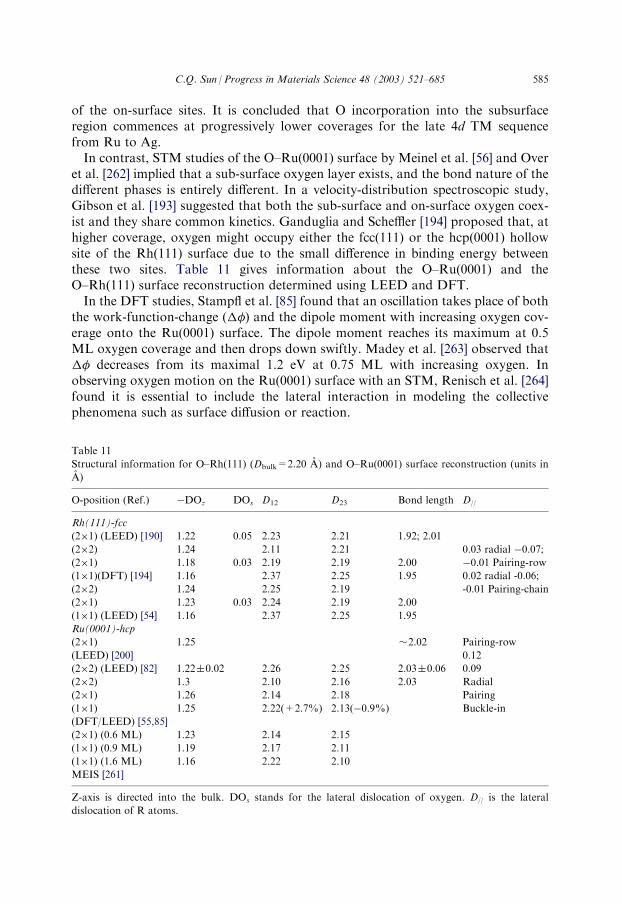
of the on-surface sites. It is concluded that O incorporation into the subsurfaceregion commences at progressively lower coverages for the late 4d TM sequencefrom Ru to Ag.In contrast, STM studies of the O–Ru(0001) surface by Meinel et al. [56] and Over
et al. [262] implied that a sub-surface oxygen layer exists, and the bond nature of thedifferent phases is entirely different. In a velocity-distribution spectroscopic study,Gibson et al. [193] suggested that both the sub-surface and on-surface oxygen coex-ist and they share common kinetics. Ganduglia and Scheffler [194] proposed that, athigher coverage, oxygen might occupy either the fcc(111) or the hcp(0001) hollowsite of the Rh(111) surface due to the small difference in binding energy betweenthese two sites. Table 11 gives information about the O–Ru(0001) and theO–Rh(111) surface reconstruction determined using LEED and DFT.In the DFT studies, Stampfl et al. [85] found that an oscillation takes place of both
the work-function-change (��) and the dipole moment with increasing oxygen cov-erage onto the Ru(0001) surface. The dipole moment reaches its maximum at 0.5ML oxygen coverage and then drops down swiftly. Madey et al. [263] observed that�� decreases from its maximal 1.2 eV at 0.75 ML with increasing oxygen. Inobserving oxygen motion on the Ru(0001) surface with an STM, Renisch et al. [264]found it is essential to include the lateral interaction in modeling the collectivephenomena such as surface diffusion or reaction.
Table 11
Structural information for O–Rh(111) (Dbulk=2.20 A) and O–Ru(0001) surface reconstruction (units in
A)
O-position (Ref.)
�DOz DOs D12 D23 Bond length D//Rh(111)-fcc
(2�1) (LEED) [190]
1.22 0.05 2.23 2.21 1.92; 2.01(2�2)
1.24 2.11 2.21 0.03 radial �0.07;�0.01 Pairing-row
0.02 radial -0.06;
-0.01 Pairing-chain
(2�1)
1.18 0.03 2.19 2.19 2.00(1�1)(DFT) [194]
1.16 2.37 2.25 1.95(2�2)
1.24 2.25 2.19(2�1)
1.23 0.03 2.24 2.19 2.00(1�1) (LEED) [54]
1.16 2.37 2.25 1.95Ru(0001)-hcp
(2�1)
1.25 �2.02 Pairing-row(LEED) [200]
0.12(2�2) (LEED) [82]
1.22�0.02 2.26 2.25 2.03�0.06 0.09(2�2)
1.3 2.10 2.16 2.03 Radial(2�1)
1.26 2.14 2.18 Pairing(1�1)
1.25 2.22(+2.7%) 2.13(�0.9%) Buckle-in(DFT/LEED) [55,85]
(2�1) (0.6 ML)
1.23 2.14 2.15(1�1) (0.9 ML)
1.19 2.17 2.11(1�1) (1.6 ML)
1.16 2.22 2.10MEIS [261]
Z-axis is directed into the bulk. DOs stands for the lateral dislocation of oxygen. D// is the lateral
dislocation of R atoms.
C.Q. Sun / Progress in Materials Science 48 (2003) 521–685 585

Fig. 18 presents the STM images for the p(2�2)-O and c(2�2)-2O phases at theRu(0001) surface. [56,199]. Fig. 19 also gives the reconstruction models for theO–Rh(111) [54,194] and O–Ru(0001) surfaces [55,85] determined by LEED andDFT. The on-surface oxygen adsorbate derives the ‘radial’ and ‘pairing-row’ struc-ture patterns at the surfaces. Similar STM patterns have been observed fromO–Au(111) [265] and Ag(111) [266] surface after prolonged annealing in oxygen(1bar) at 800 �C. These observations form the up-to-date knowledge about theO-hcp(0001) and the O-fcc(111) surface reconstruction.
3.5.2. AnalysisIt is known that the electronic configuration for Ru is 4d75s1and for Rh it is 4d85s1.
The electronegativity of both Ru and Rh is of the same value of 2.2. Their atomicradii [a=2.672(Ru) and 2.684(Rh) A] are similar. As shown in Fig. 1, the top two
Fig. 18. STM images of Ru(0001) surface with chemisorbed oxygen at 400 K. The images correspond to
(a) 0.20, (b) 0.25; and (c) 0.5 ML oxygen exposures, respectively. The p(2�2)-O (radial) and the p(2�1)-O
(pairing row) structures are fully developed at 0.25 and 0.5 ML [56].
586 C.Q. Sun / Progress in Materials Science 48 (2003) 521–685

Fig. 19. R4O cluster bonding [189,197] and the reconstruction models for the O–Rh(111) [54,194] and O–
Ru(0001) surfaces of C3v symmetry [55,85]. (a) At YO 41/4 ML coverage, O�1 locates in the center of a
tetrahedron and forms one bond with atom labeled 1. The O�1 induces and pushes the dipoles labeled 2
radially away and the C3v symmetry remains, producing the clusters of STM protrusion. (b) At YO 41/2ML, O�1 evolves into O�2 by forming one more bond with a surface R atom labeled 1. Dipoles (labeled 2)
are sustained then by the lone pairs. The dipole and ionic row move closer towards the sites without
adsorbates, which generates the pairing STM protrusion-depression patterns. (c) At YO 41.0 ML, H-likebonds dominate at the surface. Two lone pairs polarize each surface R atom (1/2) which donates mean-
while one electron to the adsorbate. Formation of the H-like bonds restores the reduced work function
and lowers the STM protrusions. The entire surface network is stabilized and becomes unreconstructed in
crystallography.
C.Q. Sun / Progress in Materials Science 48 (2003) 521–685 587
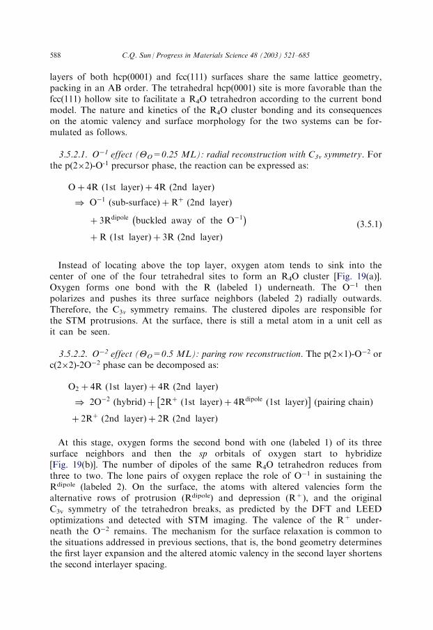
layers of both hcp(0001) and fcc(111) surfaces share the same lattice geometry,packing in an AB order. The tetrahedral hcp(0001) site is more favorable than thefcc(111) hollow site to facilitate a R4O tetrahedron according to the current bondmodel. The nature and kinetics of the R4O cluster bonding and its consequenceson the atomic valency and surface morphology for the two systems can be for-mulated as follows.
3.5.2.1. O�1 effect (YO=0.25 ML): radial reconstruction with C3v symmetry. Forthe p(2�2)-O-1 precursor phase, the reaction can be expressed as:
O þ 4R 1st layerð Þ þ 4R 2nd layerð Þ
) O�1 sub-surfaceð Þ þRþ 2nd layerð Þ
þ 3Rdipole buckled away of the O�1�
þR 1st layerð Þ þ 3R 2nd layerð Þ
ð3:5:1Þ
Instead of locating above the top layer, oxygen atom tends to sink into thecenter of one of the four tetrahedral sites to form an R4O cluster [Fig. 19(a)].Oxygen forms one bond with the R (labeled 1) underneath. The O�1 thenpolarizes and pushes its three surface neighbors (labeled 2) radially outwards.Therefore, the C3v symmetry remains. The clustered dipoles are responsible forthe STM protrusions. At the surface, there is still a metal atom in a unit cell asit can be seen.
3.5.2.2. O�2 effect (YO=0.5 ML): paring row reconstruction. The p(2�1)-O�2 orc(2�2)-2O�2 phase can be decomposed as:
O2 þ 4R 1st layerð Þ þ 4R 2nd layerð Þ
) 2O�2 hybridð Þ þ 2Rþ 1st layerð Þ þ 4Rdipole 1st layerð Þ�
pairing chainð Þ
þ 2Rþ 2nd layerð Þ þ 2R 2nd layerð Þ
At this stage, oxygen forms the second bond with one (labeled 1) of its threesurface neighbors and then the sp orbitals of oxygen start to hybridize[Fig. 19(b)]. The number of dipoles of the same R4O tetrahedron reduces fromthree to two. The lone pairs of oxygen replace the role of O�1 in sustaining theRdipole (labeled 2). On the surface, the atoms with altered valencies form thealternative rows of protrusion (Rdipole) and depression (R+), and the originalC3v symmetry of the tetrahedron breaks, as predicted by the DFT and LEEDoptimizations and detected with STM imaging. The valence of the R+ under-neath the O�2 remains. The mechanism for the surface relaxation is common tothe situations addressed in previous sections, that is, the bond geometry determinesthe first layer expansion and the altered atomic valency in the second layer shortensthe second interlayer spacing.
588 C.Q. Sun / Progress in Materials Science 48 (2003) 521–685

3.5.2.3. O�2 effect (YO=1.0 ML): H-like bond dominates. The p(1�1)-O-2 phaseon the C3v surface can be formulated as:
2O2 þ 4R 1st layerð Þ þ 4R 2nd layerð Þ
) 4O�2 hybridð Þ þ 4Rþ=dipole surfaceð Þ þ 4Rþ 2nd layerð Þ ð3:5:3Þ
As shown in Fig. 19(c), oxygen adsorbates have occupied all the tetrahedral siteson the surface. Each adsorbate needs one R atom for the bond and two to bepolarized at the surface. Because the atomic ratio O : R=1, each of the surface Ratoms has to interact with three oxygen neighbors through one ionic bond and twolone pairs. Therefore, all the R+ and Rdipole at the surface turn to be R+/dipole
(labeled 1/2) and hence H-like bonds dominate at the surface. In such a way, thesurface-dipole moment and the dipole-related �� are weakened substantially due tothe H-like bond formation, and the surface becomes unreconstructed in crystal-lography, agreeing with the DFT calculations and work function measurements, asmentioned above. This trend is the same as that occurring to the (Co, Ru)(101
-0)-
O�2 surfaces and the (Rh, Pd)(110)-O�2 surfaces at higher oxygen coverage.The analysis strongly supports the model of sub-surface oxygen formation though
most of the numerical optimizations favor an on-surface oxygen mechanism (seeTable 11) for oxygen chemisorption on these C3v surfaces. One cannot howeverexclude the possibility of multiple numerical solutions due to the correlation amongthe parameters used in optimization and the initial conditions being taken, as dis-cussed earlier. Nevertheless, existing grounds exclude the possibility that threeidentical bonds form and remain unchanged throughout the course of reaction. Ifthe oxygen is located above the top layer and if the oxygen bonds to its three surfaceneighbors identically, one could explain neither the interlayer relaxation nor theSTM protrusions. The on-surface oxygen mechanism should shrink the D12 instead,as the R+ reduces its size considerably and the R+ produces STM depressionsunder normal tip conditions.Actually, the adsorbate, whether it is O�1 or O�2, is retained always at the nearly
central position of the oxide tetrahedron throughout the course of reaction with theC3v surfaces. The striking significance of the precursor is that the O
�1 polarizes all ofits surface neighbors that maintain the original C3v symmetry. O
�2 forms two ionicbonds with the host atom in the p(2�1)-O-2 phase or electron clouds in the p(1�1)-O�2
phase, which breaks the C3v symmetry. The O�2 polarizes its two atomic neighbors
through the lone pair interaction. The O�2 should be slightly off-centered insidethe tetrahedron by an amount, which might be too small to be detectable. The oxida-tion alters the valencies of O into the O�1 and O�2, and R atoms into R+, Rdipole andR+/dipole with the measurable variation of�� and the surface dipole moment. The realprocess of oxidation is thus suggested to be that electron transport dominates andoxygen adsorbates reside inside the bulk rather than float atop the surface. This is thecase for thermal oxidation of the diamond {111} plane, which has been confirmed togo through the {111} channels throughout the course of oxidation (Section 9.1) [267].In summary, the bond model suggests that oxygen adsorbates sink into and
remain at the hcp(0001) hollow sites throughout the course of reaction with the C3v
C.Q. Sun / Progress in Materials Science 48 (2003) 521–685 589

surfaces. The rule of homo-epitaxial growth of the fcc(111) or the hcp(0001) surfaceseems unlikely. During the process of reaction, the R4O cluster configurationremains the same but the valencies of atoms at the surface change continually andsubstantially. The O�1 reconstructs the surface in a radial mode and then the O�2
produces the pairing-row pattern. Overdosing with oxygen (Y 50.5 ML) yields thep(1�1)-O�2 phase in which H-like bonds are dominant, which stabilize the surface.The H-like bond formation interlocks all the surface atoms, which may form a bar-rier for surface diffusion [268]. This conclusion should be valid for other fcc(111)and hcp(0001) surfaces with chemisorbed oxygen. For instance, a first principleapproximation of the well-defined O–Al(111) interaction [75] indicates that theadsorbate atoms prefer the hcp tetrahedral sites, 1.92 A below the topmost Al layerwhich has relaxed by 25%. A DFT calculation of Ganduglia et al. [269] suggests thatoxygen switches from the on-surface fcc site to the subsurface hcp sites of theRh(111) plane, and indicates that at even higher coverages oxygen incorporation isfollowed by oxygen agglomeration in two-dimensional sub-surface islands directlybelow the first metal layer. Inside these islands, the metastable hcp/octahedral (on-surface/sub-surface) site combination will undergo a barrierless displacement,introducing a stacking fault of the first metal layer with respect to the underlyingsubstrate and leading to a stable fcc/tetrahedral site occupation. The subsurfaceoxygen atoms in tetrahedral sites are fourfold coordinated to metal atoms. It hasbeen suggested that these elementary steps, namely, oxygen incorporation, aggrega-tion into sub-surface islands and destabilization of the metal surface may be moregeneral and precede the formation of a surface oxide at close-packed transitionmetal surfaces. A DFT calculation by Reuter et al. [270] predicted that the oxidationof the Ru(0001) surface proceeds via the accumulation of subsurface oxygen in two-dimensional islands between the first and second substrate layers. This leads locallyto a decoupling of an O–Ru–O trilayer from the underlying metal. Continued oxi-dation results in the formation and stacking of these trilayers, which unfold into theRuO2(110) rutile structure once a critical film thickness is exceeded. Along this oxi-dation pathway, they identified various metastable configurations in which oxygenoccupies the octahedral and tetrahedral sites, respectively. These configurations arefound to be rather close in energy, indicating a likely lively dynamics between themat elevated temperatures.
3.6. O–Rh(001) and (N, C)–Ni(001)
3.6.1. ObservationsWith increasing oxygen exposure of the Rh(001) surface, three outstanding phases
form sequentially, as identified using LEED, [157,164,271], STM, SPA-LEED andPES. [52,166]. The disordered p(2�2)-O phase (Y=1/4 ML) forms first and then isfollowed by the c(2�2)-2O (Y=1/2 ML) radial reconstruction and, finally, thec(2�2)p4g-2O (Y=1/2ML) clockwise-and-anticlockwise rotation of the unit cells, orclock reconstruction. These reconstruction patterns are the same as those occurringon the Ni(001) surfaces with chemisorbed carbon and nitrogen. Baraldi et al. [161–163] suggested that this sequence of phase transitions belongs to the Ising uni-
590 C.Q. Sun / Progress in Materials Science 48 (2003) 521–685

versality, or order–disorder transition. Fig. 20 shows the STM images of the twoordered phases for the O–Rh(001) surface. The oxygen adsorbate fills in the nextnearest fourfold hollow-site of the Rh(001) surface, in the same way as does oxygen onthe Cu(001) surface. It can be seen that both the c(2�2)-2O and the c(2�2)p4g-2O
Fig. 20. STM images [52] and the corresponding bond models [167] for (a) the Rh(001)-c(2�2)-2O�1
radial and (b) the c(2�2)p4g-2O�2 phases. During the reaction, a Rh5O pyramid evolves into the Rh4O
tetrahedron defining half of the surface atoms to be Rhdipole (labeled 2) and another half Rh+/dipole
(labeled 1/2). The electrostatic forces create rhombi-chains along the <11> directions. Here, (c) the
‘centered pyramid’ [272] and (d) the ‘off-centered rhombus’ [254] models are compared.
C.Q. Sun / Progress in Materials Science 48 (2003) 521–685 591

phases require the same local oxygen coverage of 1/2 ML. It was noted [52] thatformation of the two ordered phases depends not on the local oxygen coverage butrather the overall oxygen exposure. Direct LEED studies [272], revealed, however,that oxygen resides in hollow sites of the Ni(001) surface; the first substrate layerdistance is expanded and the second substrate layer reconstructs into a buckledlayer. It is suggested that [273] bond form between oxygen and the second-layernickel atom below it. No apparent rotation was identified [274].Fig. 21 shows the STM images of the ordered Ni(001)-(2�2)p4g-2C [287] and
Ni(001)-(2�2)p4g-2N [286] surfaces that exhibit the same type of ‘clock’ recon-struction as that occurring on the O–Rh(001) surface albeit the slight difference inthe rotation angles. However, the calculated STM image shows the C atoms asdepressions while in the experiment, a small protrusion is suggested [275]. It isinteresting to note that the Ni(100)-(2�2)p4g-2N STM image exhibits two orienta-tions of the depressions. With slight deviation, one is along the [10] direction and the
Fig. 21. STM images [286,287] and the corresponding atomic and bond model (insertions) for Ni(001)-
(2�2)p4g-(C�4, N�3) clock reconstruction. Individual atomic valencies and the orientation of the depres-
sions are indicated. Although they appeared quite similar to that of the Rh(001)-(2�2)p4g-O�2 phase, the
surface atomic valencies and the driving force are different.
592 C.Q. Sun / Progress in Materials Science 48 (2003) 521–685

other closes to the [01] direction. This provides the opportunity for one to identifythe atomic valencies at the surface.In 1979, Onuferko et al. [276] proposed a centered-pyramid model [Fig. 20(c)] for
the ‘p4g’ reconstruction. The model indicates that a ‘stress release’ mechanism pro-vides forces driving the ‘radial’ reconstruction phase to transit into the ‘clock’ rota-tion. The oxygen adsorbate was determined to locate DOz > 0.6 A156 above the C4vhollow site and form a centered-pyramid with the four Rh atoms at the surface. Itwas interpreted that the compressive stress of the pyramid in the Rh(001)-c(2�2)-2Osurface is released through the rotation of the Rh4O pyramid. The release of stressprovides the forces that drive the reconstruction while the basic R4O pyramidremains during the process of reconstruction despite a slight change of the verticalposition of the oxygen. This model applied well to all the (N, C)–Ni(001) and theO–Rh(001) surface reconstructions.In 1998, Alfe et al. [160,161,277] suggested an alternative (Fig. 20d) for the
Rh(001)-c(2�2)p4g-2O second phase. Instead of forming a pyramid with the foursurface neighbors in the C4v hollow site, the adsorbate was assumed to prefer the siteeccentrically above the ‘rhombus’. It is suggested that the adsorbate jumps back andforth along the longer axis of the rhombus. Norris et al. [278] derived from XRDmeasurement that, in the second ‘p4g’ phase, the Rh atom is displaced by 0.19�0.02A in the plane along the <11> direction. The oxygen atom is situated in therhombus sites with an in-plane shift of 0.20�0.05 A on either side of the center. The‘off-centered-rhombus’ model leads to the conclusion [161] that for all the Rh{(001),(110), (111)} surfaces at medium-high oxygen coverage, oxygen adsorbate tends tolocates at an apical site of a tetrahedron and to form three identical bonds with theRh atoms. So formed Rh3O tetrahedron was taken to be a C3v point-group sym-metry and the lengths of all the three O–Rh bonds in the Rh{(001), (110), (111)}surfaces to be in the range of 2.00–2.06 A. The Rh–O–Rh bond angle was suggestedto be around 90�. DFT calculations suggested that the ‘off-centered rhombus’ modelis less favorable than the ‘centered-pyramid’ model for the (C, N)–Ni(001) surfaces[277]. Table 12 summarizes the geometrical information for the ‘p4g’ reconstructionfor the Rh(001)-c(2�2)p4g-2O and the Ni(001)-c(2�2)p4g-2(C, N) surfaces.Kirsch and Harris [279] calculated surface reconstructions of Ni(001) surface
induced by C, N and O adsorption and suggested that C and N atoms prefer thenearly coplanar sites with the top Ni surface and induce the ‘‘clock’’ reconstructionof the surface while O atoms prefer sites slightly above the Ni(100) surface plane andhave little effect on the overall surface structure. The local environments of the C, N,and O atoms on these surfaces are similar to their environments in a series of latetransition metal carbonyl clusters, suggesting that some of the same electronic fac-tors may play a role in favouring the different structures. Results of the calculationssuggest that when adsorbates occupy coplanar sites on Ni(100), much of the Ni–Nibonding within the surface layer and between the surface- and second-layers is dis-rupted. On the C- and N-covered surfaces the disruption is more than compensatedfor by the formation of strong adsorbate–Ni bonds and by new Ni–Ni surface bondsresulting from the clock reconstruction. When O is forced into a coplanar site,however, both the higher electron count and increased electronegativity of the O
C.Q. Sun / Progress in Materials Science 48 (2003) 521–685 593

atoms lead to severe disruption of the surface bonding and weak Ni–O bonds. WhenO atoms sit above the surface, they form more polar Ni–O bonds, contribute lesselectron density to the Ni surface bands, and cause less disruption to Ni–Ni surfacebonds. These results suggest that, similar to the organometallic clusters, the sitepreferences of C, N, and O atoms are directly related to their electron count, and inturn to the relative occupation of both Ni–Ni and X–Ni (X=C, N, O) antibondingbands.
3.6.2. AnalysisWe now show that the O–Rh(001) radial and the subsequent clock reconstruction
results from the formation of the oxide tetrahedron, in which the O�1 transits to anO�2 with sp-orbital hybridization. The sp-orbital hybridization also holds for the Cand N when they react with the Ni(001) surface. It is derived that the electrostaticforce due to charge redistribution drives the p4g reconstruction [100,288,289]. Thebalance of bond tension against the electrostatic force along the <11> directionstabilizes the clock rotation on the O–Rh(001) and N–Ni(001) surfaces. However,equilibrium of electrostatic repulsion along the <11> direction and a response ofbond compression stabilize the C–Ni(001) clock rotation. Although the patterns ofreconstruction and morphology for the O–Rh(001) and the (C, N)–Ni(001) surfacesare nearly the same, the surface atomic valencies and the driving forces are differentdue to different valencies of the C�4, N�3 and O�2. The O–Rh bond experiencestension rather than compression.
Table 12
Atomic geometry of the Rh(001)-c(2�2)p4g-2O surface (D12=1.902 A; z is directed into the bulk) and the
Ni(001)-c(2�2)p4g-2(C, N) surfaces
Model [Ref.]
DOz DOs D<11> D12 D23Off-centered
rhombus model
[254] for
O–Rh(001)
O-Rh(001)
(LEED) [161]
�1.01�0.05
0.29�0.15 0.2�0.07 1.94�0.05 1.87�0.03(DFT) [160]
�1.02 0.08�0.20 1.99DFT [277]
�1.00�0.04 0.21 0.35 1.922SXRD [278]
�0.64�0.06 0.20�0.05 0.19�0.02 1.96�0.05Centered
pyramid model
[276] for all the
‘p4g’
N-Ni(001) (IES) [156]
�0.6�0.1 0.2�0.1SEAFS [280,281]
0.77�0.10PED [282]
�0.25�0.05 0.55�0.20 +0.15�0.10SXRD [283]
�0.20�0.10 0.30�0.01 +0.17�0.01C–Ni(001), PED [282]
�0.30�0.05 0.55�0.20 +0.15�0.10LEED [276]
�0.30�0.12 0.35�0.05 +0.20�0.05SEXAFS [284]
�0.2�0. 2LEED [285]
�0.31�0.05 0.45�0.07 +0.19�0.04Rhombus chain
model [100] for
all the ‘p4g’
Rh2O [100] +STM [52]
> 0 > 0 0.3Ni3N [100] + STM [286]
> 0 > 0 0.37Ni4C [100] +STM [287]
> 0 > 0 0.64594 C.Q. Sun / Progress in Materials Science 48 (2003) 521–685

With the bond model, the Rh(001)-c(2�2)-2O�1 radial and the subsequentRh(001)-(2�2)p4g-2O�2 clock reconstruction can be formulated as follows [Fig. 20(aand b)]:
O2 adsorbateð Þ þ 4Rh surfaceð Þ þ 4Rh 2nd layerð Þ
) 2O�1 sub-surfaceð Þ þ 2Rh þ 2nd layerð Þ
þ 2Rh 2nd layerð Þ þ 4Rhdipole O�1-induced� ð3:6:1Þ
this O�1-induced phase transits into the Rh(001)-(2�2)p4g-2O�2 second phase (seethe corresponding deformed unit cell in Fig. 20b):
) 2O�2 hybridð Þ þ 2Rhþ 2nd layerð Þ þ 2Rhþ=dipole
þ 2Rh 2nd layerð Þ þ 2Rhdipole O�2-induced� ð3:6:2Þ
Similarly, the Ni(001)-(2�2)p4g-2(N�3, C�4) surfaces can be formulated as(Fig. 21) [100]:
N2 adsorbateð Þ þ 4Ni surfaceð Þ þ 4Ni 2nd layerð Þ
) 2N�3 hybridð Þ þ 2Niþ surfaceð Þ þ 2Niþ=dipole surfaceð Þ
þ 2Niþ 2nd layerð Þ þ 2Ni 2nd layerð Þ
ð3:6:3Þ
and,
C2 adsorbateð Þ þ 4Ni surfaceð Þ þ 4Ni 2nd layerð Þ
) 2C�4 hybridð Þ þ 2Niþ surfaceð Þ þ 2Ni2þ surfaceð Þ
þ 2Niþ 2nd layerð Þ þ 2Ni 2nd layerð Þð3:6:4Þ
It is to be noted that from the rhombi-chain formation point of view, the p4gSTM images induced by C�4, N�3 and O�2 are substantially the same despite therotation angles. However, Ni(001)-(2�2)p4g-N�3 STM image shows two apparentorientations of the alternative thick lines of depressions, with slight deviation fromthe [10] direction and the [01] direction. Linking the Ni+ ions labeled 1 in N–Ni(001)surface [see Fig. 21(b)], one can find that the 1–1 bridge matches ideally the orien-tations of the STM depressions. This verifies that the radius of a Ni+ ion is muchsmaller than that of a Ni+/dipole. Therefore, applying the model of bonding to theSTM images enables the individual atomic valencies of the surface Ni atoms to beidentified.Table 13 summarizes information for the C�4, N�3 and O�2 derived ‘p4g’ phases
on the Ni(001) and Rh(001) surfaces. For instance, oxygen sinks into the C4v hollowsite in the Rh(001) surface and bonds to the Rh atom underneath. An Rh5O clusterforms in the c(2�2)-2O�1 precursor phase. The O�1 polarizes and pushes the elec-tron cloud of the surface atoms radially away from the central adsorbate. In thesecond phase, the c(2�2) cell deforms into two rhombi (without adsorbate) and two
C.Q. Sun / Progress in Materials Science 48 (2003) 521–685 595

squares with adsorbates inside, as can be seen from Fig. 20(b). The Rh5O pyramidwill evolve into an Rh4O tetrahedron with an off-centered shift of the adsorbate inthe hollow and one Rh atom at surface was released from the original Rh5O pyr-amid. As the O�2 has already bonded to one Rh underneath, the tetrahedron definesone Rh+ (labeled 1) and two lone-pair-induced Rhdipole dipoles (labeled 2) of thefour nearest surface neighbors. The Rh5O ! Rh4O transition gives rise to theoverall ‘p4g’ reconstruction. As can be seen from the primary unit cell containingthe adsorbate [Fig. 20(b)], three of the four surface neighbors are labeled with 1, 2and 2, respectively. Because the surface atomic ratio O : Rh=1 : 2 and each oxygenbonds to one atom at surface and needs two atoms to be polarized, half of theoverall surface atoms are thus defined as Rhdipole and another half as Rh+/dipole. TheRh+/dipole contributes to the H-like bond. One can find that atoms labeled 1 changetheir positions in a clockwise fashion if one counts the O-occupied hollows along the<11> direction (gray thick lines). The adsorbate dislocates eccentrically in direc-tion in a periodic way. From this point of view, it would be essential and complete toconsider a c(4
p2�4
p2)R45�-16O�2 complex unit cell in practice due to the peri-
odicity of the off-centered adsorbate positions. Strikingly, the ‘rhombi’ hollowswithout adsorbates form chains along the <11> direction. The above argument isalso applicable to the (N�3, C�4)-Ni(001) surfaces.From the atomic structure point of view, the current description favors both the
existing models to a certain extent. Oxygen prefers the site inside (sub-surface) theC4v hollow (Onuferko’s model) and eccentrically (Alfe’s model) in a periodic way(detected as oscillation). It is understandable that periodicity can be detected asoscillation. Most importantly, specification of the valencies of the adsorbates givesgreat detail about the electronic structures, driving forces and bond stresses, of theRh(001)–O and the Ni(001)–(C, N) surfaces [100]. Although the STM and LEEDsignatures appeared the same for these three ‘p4g’ reconstructed surfaces derived byC, N and O, the underlying mechanisms are quite different. Therefore, the reactionis a process in which charge transportation dominates. What one often observeswith STM and LEED is simply a portion of the consequences. For more detailsregarding the sp-orbital hybrid bonding of C, N, and O to the fcc(001) surfaces ofRh and Ni please refer to a recent report [100].
Table 13
Summary of the geometrical change, driving force, Fi, and bond tension, T, of the ‘p4g’ clock rotation (2)
derived from the STM images with the current model [100]
(2�2)p4g
Rh(100)-O-2 Ni(100)-N-3 Ni(100)-C-4Rotation angle F (�)
0.0; 9.0 0.0; 12.0 0.0; 20.0S<11> (A)
0.00; 0.30 0.00; 0.37 0.00; 0.64Bond strain �L/L (%)
1.2 2.2 6.4Electrostatic forces Fi
7.99; 11.09 8.21; 14.59 �3.11;�91.17Bond stress Fb (dyn)
35.16 35.95 �133.00Surface atomic states
Dipole; +/dipole +; +/dipole +; 2+596 C.Q. Sun / Progress in Materials Science 48 (2003) 521–685

3.6.3. Quantification: driving force and bond stressOne can estimate the lateral displacements of the Rh atoms by measuring the
sharp angle � of a rhombus in the STM image [Fig. 20(b)]. The average value of � ismeasured as 72�. The unit cell containing O�2 adsorbate rotates, hence, 2=(90���)/2=9�, which displaces the Rh atom along the <11> direction byS<11>=
p2R�tg2=0.30 A, where R=1.342 A is the atomic radius of Rh. Table 13
summarizes the geometrical change, driving force, Fi, and bond stress, T, of the ‘p4g’clock rotation (2) derived from the C�4, N�3 and O�2 induced ‘p4g’ reconstructionon the fcc(001) surface of Rh and Ni [100].Inspecting Figs. 20(b) and 21 one can find that the surface network is composed of
one-dimensional ‘- 2 - (1/2) – (1/2) - 2 – 2 - (1/2) – (1/2)-’ rhombi-chains along the<11> directions. Label 1 and 2 represents the valencies of ‘+’ and ‘dipole’,respectively. The electrostatic charges of the Rh+/dipole (1/2) and the Rhdipole (2) arenot equal and the Rh+/dipole is slightly positive compared to the Rhdipole that has anegative feature. The intensity of interaction is in such an order: 2 - 2 � (1/2) - (1/2)> 0 > (1/2) - 2. The repulsion between the 2 - 2 or (1/2) - (1/2) and the slightattraction between the 2 - (1/2) determines that the distance of 2 - 2 or (1/2) - (1/2) islonger than the distance of (1/2) - 2. Rhombus formation displaces the Rh atomsalong the <11> direction, and consequently, leads to the overall rhombi-chainnetwork at the surface. The alternate attraction and repulsion along the chain willsqueeze the 2-(1/2) closer without otherwise a response of bond tension to equili-brate the electrostatic force along the chain. From Fig. 22(a and b), it is seen that thebond expands by an amount �L/L=1/cosF�1=1.2%, which is negligibly smalland, therefore, a mechanism of bond-tension-increase rather than the mechanism ofbond-compression-release dominates in the Rh(001)p4g-(2�2)-2O�2 or the Rh(001)-(4p2�4
p2)R45�-16O�2 phase transition.
Without knowing the exact dipole moment, one may assume that Cou-lomb interaction dominates along the rhombi-chain that contains infinitenumber of atoms (n 5�100 is sufficient for calculation). The Coulombpotential Vi and the electrostatic force Fi acting on the ith atom in therhombi-chain are:
Vi ¼1
4�"0
Xi 6¼j
qj
rij¼
1
4�"0
Xi 6¼j
�1ð Þj 1
2j � 1ð Þa � 2s�
1
2j� 1ð Þa þ 2s
� �
Fi ¼ �qi@Vi
@rð3:6:6Þ
The relative charges for Rhdipole and Rh+/dipole are defined as qi=�"e and "e,respectively, by introducing an effective charge factor "="c + �' ("i�"c)/2 whichtakes the valence screening effect into account. "c=0.5 (�'=0) and "i=1.0 (�'=2)correspond to covalent and ionic states, respectively. For the current O–Rh system,��=3.5� 2.2=1.3, "=0.825.As a component of the electrostatic force Fi, the Fb in Fig. 22(b) balances the bond
tension T and hence the clock rotation of the unit cell:
C.Q. Sun / Progress in Materials Science 48 (2003) 521–685 597

Fb ¼Fiffiffiffiffiffiffiffiffiffiffiffiffiffiffiffiffiffiffiffiffiffiffiffiffiffiffiffiffiffiffiffiffiffiffiffiffiffiffiffiffiffiffiffiffiffi
2 1þ cos 2 90� � Fð Þð Þ½ �p ð3:6:7Þ
When the Rh4O tetrahedron rotates from 0 to 9� (see Table 13), S<11> shifts from0 to 0.3 A and the electrostatic force Fi increases from 8 to 11 dyn. The tensile bondstress, T, increases to 35 dyn at F=9�. It is easy to understand that, at F <9�, T<Fb, while at F > 9�, T > Fb. Therefore, the coupling of the alternative electro-static attraction and repulsion along the rhombus chain with the response of bondtension stabilizes the rotation.The bond tension might be over-estimated because the dipole potential should
take the rij�6 form rather than the simple Coulomb potential. However, this can be
precisely determined provided there is a known dipole moment. Nevertheless, wehave justified that the driving force behind the Rh(001)-O�2 clock rotation comesfrom the electrostatic interaction along the rhombi-chain and further rotation of thetetrahedron is constrained by the response of a bond tension. This bond-tension-increase mechanism also holds for the Ni(001)-N�3 surface. The Ni(001)-C�4 rota-
Fig. 22. (a) The non-uniform ‘- 2 - 1/2 – 1/2 - 2 -’ rhombi-chain is extracted from Figs. 20(b) and 21 to
estimate (b) the atomic dislocation and (c) the driving force and bond stress. Labels 2 and 1/2 stand for
different valencies (refer to Table 13) for O�2, N�3 and C�4 induced chains. The clock rotation angle F isderived from the STM rhombus sharp-angle Y. F=(90��Y)/2; S=
p2R� tgF; �L/L=1/cosF�1; Fi is
decomposed as Fb. (c) Shows the rotation angle dependence of the driving force Fi. Rotation is stabilized
at 9� by T=Fb. If F > 9�, T > Fb; otherwise, T <Fb.
598 C.Q. Sun / Progress in Materials Science 48 (2003) 521–685

tion is driven by the nonequivalent electrostatic repulsion in the <11> directionand the rotation is balanced by the response of bond-compression-increase, instead[100].
3.7. O–(Ag, V)(001)
3.7.1. O–Ag(001)
3.7.1.1. Observations. Using a combination of LEED and HREELS, Fang [290]found that oxygen could induce two different phases on the Ag(001) surface. At lowtemperature, the system displays a c(2�2) LEED pattern with an EELS peak at 37meV. By increasing the temperature from 180 to 300 K, a transition to a (1�1)LEED pattern happens, and the EELS peak shifts from 37 meV to a lower value of30 meV. The EELS peak shift indicates that the stretch interaction of oxygen-adsorbate is weakened. This phase transition was found to be reversible. It is inter-preted that the high-temperature (1�1) structure correspond to full oxygen coverage(0=1 ML), while the low-temperature c(2�2) structure arise from a lower coverage(0=0.5 ML), with a substantial amount of oxygen adsorbed in subsurface.Recently, Rocca et al. [291] reported a more complete investigation of O–Ag(001)surface, using the techniques of LEED, HREELS, XPS, and XPD. Measurementsconfirmed the existence of the phase transition observed by Fang, but leads to adifferent structural model. The estimated oxygen coverage is never greater than 0.4ML. By fitting the surface geometry to high-temperature XPD results, it was pre-dicted that atomic oxygen would sit in the fourfold hollow site, while at low tem-perature the fit of XPD data suggests that the substrate undergoes a (
p2�2
p2)R45�
missing-row reconstruction, being the same to the O-Cu(001) second phase with theCu3O2 pairing-tetrahedron configuration. In the second phase, oxygen atoms sit inthe hollow sites near the Ag missing rows of the substrate, thus giving rise to ac(2�2) LEED pattern. A first principle DFT calculation by Cipriani et al. [292]examined the phase stability at different oxygen coverage. It was found that themissing-row reconstruction is almost degenerate in energy with the non-recon-structed c(2�2) structure, both of which share the same LEED pattern. The geo-metrical details of the DFT calculation structure slightly differ from those inferredfrom XPD measurements [290]. Both the local density approximation (LDA) andthe generalized gradient approximation (GGA) predicted that the surface fourfold-coordinated hollow site and the sub-surface fivefold-coordinated hollow site aremost stable, practically degenerated, and separated by an energy barrier of �25meV or less. It is striking to note that the first Ag interlayer spacing expands by upto 30% upon oxygen adsorption [292]. According to the XPD results [291], oxygenadsorbates displace laterally by 0.36 A toward the missing row and shift verticallyby 0.15 A down below the top Ag atoms. The Ag atoms close to the missing row areshifted up by 0.3 A and laterally by a negligible amount. In the calculated structure,oxygen atoms sit �0.3 A above the Ag atoms that moves �0.2 A close to themissing row and �0.1 A below the other surface atoms. Oxygen atoms do not relaxlaterally. However, the origin of the structural discrepancy is unclear. Nonetheless,
C.Q. Sun / Progress in Materials Science 48 (2003) 521–685 599

the overall missing row structure coincides with the Cu(001)-(p2�2
p2)R45�-2O�2
phase which is dominated by the Cu3O2 structure where oxygen atoms move awayfrom the missing row and go below the Cu atoms near the missing row for the tet-rahedron formation. The Cu (dipoles) are shifted up and relax laterally towards themissing row by �0.25 A to form the ‘dumb bell’ protrusion cross over the missingrow. As discussed previously, accurate determination of the static position of atomsis not practical as the reaction is a kinetic process. In addition, errors are ofteninvolved in measurement and approximations in theoretical determination as well.The significant difference between the O–Cu(001) and the O–Ag(001) is the critical
temperature for phase transition. Missing row forms at the O–Cu(001) surface at�700 K while it forms at the O–Ag(001) surface below 300 K. XPS profiles [291]from O–Ag(001) show that the O 1s lower binding energy (528.3 eV) componentincreases its intensity with temperature rise at an expenses of decreasing the highbinding energy (530.9 eV) peak that dominates at T4300 K. This is also in line withthe 37!30 meV EELS peak transition. The transition of both the XPS bindingenergy and the EELS stretch energy indicates that the O–Ag(001) surface undergoesa phase transition from stable to quasi-stable at �300 K or lower with temperaturerise. At 246 K, the stable phase forms gradually with aging time. The stable phaseformation completes after a 3200 s aging at 246 K.With oxygen adsorption, an additional DOS feature at �2.0 to �3.0 eV emerges
[291,293] which agrees with those observed from the O–Ag(110) (�1.5��3.3 eV)[294] and O–Ag(111) (�2.0 eV) [295] surfaces. These features were attributed to thecontribution from O 2p states [291] while we have ascribed them as contributionfrom non-bonding lone pairs of O�2.
3.7.1.2. Analysis. It is interesting to note that the O–Ag(001) bi-phase structuresare partly analogies of the O–Rh(001) and the O–Cu(001) surfaces. The fivefoldcoordinated oxygen is the same as that in the Rh(001)-c(2�2)-2O�1 first phase andthe low temperature missing-row structure is the same as the Cu(001)-(p2�2
p2)R45�-2O�2 second phase. Formulae of reaction and the surface atomic
valencies of these two phases may refer to the conventions of the correspondingRh(001)-O-1 and Cu(001)-O-2 phases (Sections 3.3.2 and 3.2.2, respectively). Neitherlike the transition from CuO2 paring-pyramid to the Cu3O2 pairing tetrahedron atthe Cu(001) surface nor the transition from the Rh5O to the rotated Rh4O at theRh(001) surface, the O–Ag(001) surface transits from the Ag5O (O–Rh(001) firstphase) to the Ag3O2 [O–Cu(001] second phase] at much lower critical temperature.This intriguing fashion of low-temperature phase transition may originate from thelow electronegativity (1.9) and the large atomic size (rAg=1.442 A) of Ag atom (seeTable 1). At the low temperature, O�2 is more stable than the O�1 according to theXPS and EELS spectral features.The valence DOS features agree with that detected from other oxide surfaces.
These features can be unambiguously specified as the contribution from the non-bonding lone pairs of oxygen upon the sp-orbital hybridization. The transition ofXPS O 1s peak energy and the EELS stretch vibration are indication of oxygen de-hybridization, which happens to the O–Cu(001) at about 700 K [209].
600 C.Q. Sun / Progress in Materials Science 48 (2003) 521–685

3.7.2. O–V(001)3.7.2.1. Observations. With the STM, LEED, and DFT approaches, Koller et al.
[296] investigated the O-induced V(001) surface reconstruction. The STM images inFig. 23 show apparently the bi-phase structures beside the visible dark linesarranged regularly at the surface along the <100> directions. The distancebetween the dark lines is usually 4–6 vanadium <100> lattice constants, and,therefore, a (1�5) reconstruction mode was suggested. In the simulated STM ima-ges, the fourfold hollow sites occupied by oxygen atoms appeared as dark spotswhile the unoccupied hollow sites remain bright. The first phase within the domainis the same as the Rh(001)-c(2�2)-2O�1 phase [see Fig. 20(a)]. Oxygen occupies thenext nearest fourfold hollow-site and induces the radial reconstruction, as indicatedin the STM image (b). AES detected oxygen coverage as 2/3 ML. With increasingoxygen coverage to �0.73 ML, the second phase appears, in which the dark linesremain. The short-ordered, zigzagged ‘O–O’ chains run along the <11> direction.The bright spot is composed of four atoms. Ab initio calculations at very low oxy-gen coverage revealed that the C4v-hollow sited oxygen along the dark lines is ener-getically most favorable (�4.89 eV, Fig. 24a) and is followed by the twofold-coordinated bridge site (�3.17 eV) and then the site atop a vanadium atom (�2.97eV). The optimal structures at higher oxygen coverage are given in Fig. 24(b, c) withcorresponding binding energies of �5.26 eV and �5.20 eV, respectively. One shouldnote that the oxygen atoms in the dark lines now prefer the bridge sites in the twophases involving the reconstructed domains compared with the initial phase ofoxidation.LEED optimisation [296] with a total number of 26 independent parameters leads
to a structural model for the second phase (Fig. 24d, with R-factor value of 0.17),which is inconsistent with the models derived from STM imaging and ab initio cal-culations. The oxygen atoms in the bridge sites reside 0.12–0.18 A above the topvanadium layer, while the oxygen atoms in the C4v-hollow sites are �0.5 A abovethe top layer. The structural discrepancy determined by different methods wasattributed to: (i) the ab initio data are for T=0 K, whereas the LEED was taken atroom temperature; (ii) the involvement of the (1�4) and (1�6) superstructures mayinfluence the LEED measurements. Nevertheless, both the LEED and DFT opti-mization revealed an expansion of the first layer spacing (+4.2%) and a contraction(�3.2%) of the second with respect to the clean V(001) surface that contracts by�7��8.5% (determined by LEED) or �15% (by DFT).
3.7.2.2. Analysis. Disregarding the accuracy in the vertical positions of the oxy-gen atoms in the dark lines, the bi-phase structure for the O–V(001) surface can beeasily formulated. The formula for the first O�1-derived phase may refer to that forthe Rh(001)-c(2�2)-2O�1(Y=1/2 ML) surface which showed the radial recon-struction (Section 3.6.2). The oxygen forms a bond with a Vanadium atom under-neath and then polarizes the surface neighbors, which form the V5O structure.With the increase of oxygen coverage, the O�1 evolves into the O�2 that givesrise to the short-ordered (
p2�3
p2)R45�-4O�2 phase, which can be formulated as
follows:
C.Q. Sun / Progress in Materials Science 48 (2003) 521–685 601
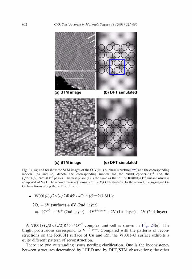
� V(001)-(p2�3
p2)R45�- 4O�2 (Y=2/3 ML):
2O2 þ 6V surfaceð Þ þ 6V 2nd layerð Þ
) 4O�2 þ 4Vþ 2nd layerð Þ þ 4Vþ=dipole þ 2V 1st layerð Þ þ 2V 2nd layerð Þ
A V(001)-(p2�3
p2)R45�-4O�2 complex unit cell is shown in Fig. 24(e). The
bright protrusions correspond to V+/dipole. Compared with the patterns of recon-structions on the fcc(001) surface of Cu and Rh, the V(001)–O surface exhibits aquite different pattern of reconstruction.There are two outstanding issues needing clarification. One is the inconsistency
between structures determined by LEED and by DFT/STM observations; the other
Fig. 23. (a) and (c) show the STM images of the O–V(001) bi-phase structure [296] and the corresponding
models. (b) and (d) denote the corresponding models for the V(001)-c(2�2)-2O�1 and the
(p2�3
p2)R45�-4O�2 phases. The first phase (a) is the same as that of the Rh(001)-O�1 surface which is
composed of V5O. The second phase (c) consists of the V4O tetrahedron. In the second, the zigzagged O–
O chain forms along the <11> direction.
602 C.Q. Sun / Progress in Materials Science 48 (2003) 521–685

is the oxygen coverage. AES detected higher oxygen coverage (0.67 and �0.73 MLfor the two phases, respectively) but the model gives only 1/2 and 2/3 ML ideally forthe two corresponding phases. The structural discrepancy may arise from the hugeparameter space that warrants non-unique solutions [99]. The agreement between theSTM and the DFT results supports each other, which may indicate the essentialityof searching for other possible numerical solutions in LEED optimization, such assub-surface oxygen. Modeling analysis conducted here insofar indicates that theoxygen atom always tends to be located inside the tetrahedron. On the other hand,the V atoms in the center of the bright protrusions are expected to be missing asthese V atoms interact with no oxygen atoms but they experience strong repulsion
Fig. 24. Comparison of the structural models. Ab initio optimization of (a) the C4v-hollow sited oxygen in
the dark lines and the arrangement of oxygen for (b) the first and the (c) second phase as observed with
STM. Panel (d) shows the LEED optimal structural model for the reconstructed surface at higher oxygen
coverage. Panel (e) is the current bond model suggesting a short-ordered V(001)-(p2�3
p2)R45�-4O�2
(2/3 ML) reconstruction.
C.Q. Sun / Progress in Materials Science 48 (2003) 521–685 603

from the neighboring V+/dipole. The expected missing V atoms may reduce thenumber of V atoms at the surface layers. In addition, the density of oxygen in thedark lines may be higher than the oxygen atoms inside the reconstructed domains.This may further increase the surface atomic ratio of O : V. These two factors,would account for the difference in the oxygen coverage between the AES measure-ment and the model specification. Further confirmation of the missing row forma-tion at the V(001)-O surface is needed.It is interesting to compare the O–(Cu, Rh, Ag, V)-(001) surface reconstruction.
The different atomic sizes and different values of electronegativity give rise tothe entirely different patterns of reconstruction on the four surfaces of the samelattice geometry. The process of tetrahedron bond formation is the same despitethe different transition temperatures and the corresponding patterns of observations.
4. STS and PES: valence DOS
4.1. Signature generality
Chemisorption is a process in which chemical bond forms and the valence electronstransport among the bonding constituent atoms. Processes of charge transport modifythe valence band structure and introduce additional DOS features. The derived DOSfeatures are detectable using STS (around EF), PES (E<EF), and IPES (inverse PES,E>EF). The database for the oxygen-derivedDOS for metals has been well established.However, identification of the DOS features in the valence band and above is still underdebate and a clear definition of the DOS features is necessary.
4.1.1. STSSTS measurements can be carried out by recording the dIt/dVt�Vt or d(lnIt)/
d(lnVt)�Vt curves, at a constant tip current, It, and various tip voltages, Vt. Thefeatures of an STS spectrum are associated with the on-site DOS of a few atoms at asurface [297,298]. Features below EF (tip negative bias) correspond to the occupiedDOS at the surface while features above EF (tip positive) represent the allowed, yetunoccupied, DOS of the sample surface [16].Fig. 25 shows the STS spectra of a Cu(110) surface [47] and of an Nb(110) surface
[304] with and without chemisorbed oxygen. In the first panel, spectrum A wastaken from the clean Cu(110) surface while B and C were taken from, respectively,the site above the bright spot (dipole) and the site between two bright spots along a‘O�2 : Cudipole : O�2’ chain at the Cu(110)-(2�1)-O�2 surface (Fig. 6 in Section 3.2).On the clean surface, empty DOS of 0.8–1.8 eV above EF are resolved and no extraDOS structures are found below EF. The STS spectra recorded from theCu(110)-(2�1)-O�2 islands reveal that the original empty-DOS above EF are par-tially occupied by electrons upon chemisorption, which result in a slight shift of theempty DOS to higher energy. Additional DOS features are generated around �2.1eV below the EF. The sharp features around �1.4 eV have been detected withARPES [233] and with the de-excitation spectroscopy of metastable atoms [300]. The
604 C.Q. Sun / Progress in Materials Science 48 (2003) 521–685

Cu–3d DOS are between �2 and �5 eV [35,233,301], and the O–Cu bonding deriva-tives are around the 2p-level of oxygen, �5.6 to �7.8 eV below EF [302]. Both Cu–3dand O–Cu bond DOS features are outside the energy range of the STS (EF�2.5 eV).Recently, Uehara et al. [303] measured from the O–Cu(110) surface a 2.3 eV peak
using the STM light-emission spectra. This feature was associated with the electrontransition from the Cu 4s–4p hybridized orbitals of Cu to the empty O-2p orbitals.It is to be noted that the STS features of spectrum C (taken from between the
bright spots) is more pronounced than that of spectrum B. Taking the tip-size effect
Fig. 25. STS profiles of (a) a Cu(110) surface [47] and of (b) a Nb(110) surface [304] with and without
chemisorbed oxygen. Spectra in panel (a) were obtained (A) at a metallic region, (B) on top of, and, (C)
between protrusions of the ‘O�2 : Cudipole : O�2 :’ chain [299] on the Cu(110)-(2�1)-O�2 surface. Insert in
panel (b) shows the STM image of O–Nb(110) surface with O–Nb chains and triangle-shaped atomic
vacancies.
C.Q. Sun / Progress in Materials Science 48 (2003) 521–685 605

of an STS (with �2.5 A lateral uncertainty) and the constant current mode intoaccount, the origin of the intensity difference between spectra B and C can easily beunderstood. Spectrum C is taken from the depression (inward curvature) that is atopan oxygen adsorbate. The above-EF feature is dominated by the two neighboringdipole protrusions while the below-EF information comes from the lone pair of theO�2 underneath. Thus, it is understandable that the above-EF features of profile Care stronger than those of profile B as profile C is collected mainly from a dipole(from outward curvature) site. The tip above the dipole collects information of boththe lone pair and the dipole but the information is relatively weaker because of thepositive curvature at the dipole site. So the intensity of an STS spectrum is deter-mined by (i) the tip size, (ii) the on-site curvature and, (iii) the energy states of O�2
adsorbate (<EF, lone pair electrons) and Cudipole (>EF, polarized electron).Therefore, the origin for the new peaks at �2.1 eV and the shift of the surface statesat 0.8–1.8 eV become clear now with the current BBB modeling specifications [299].STS spectra in a broader energy range (�8, 8 eV) from the O–Nd(110) surface
(Fig. 25) show DOS features near to the EF of O–Nb(110) is not that apparent asfrom the O–Cu–O chain [304]. They are rather weak compared with the intenseresonant features. The resonant peaks at positive bias (unoccupied states) wereassigned to a tunneling via quantized states in a potential well induced by the com-bination of image states and the applied electrical field [305,306]. Since the lowestimage state is energetically tied to the vacuum level, the position of the first reso-nance can be used for an estimation of the work function [306]. The successivehigher resonance at 6.4 and 7.7 eV are in accordance with resonance found for othertransition metals such as Cu/Mo(110) [305] and Ni(001) surfaces [306,307]. Theseresonances are shifted to lower energies on the O–Nb surfaces, independent of thetip positions, i.e., on or away from the O–Nb chains. The resonance shift was related tothe variation of work function upon oxidation [304]. During oxygen chemisorption atroom temperature an initial decrease by ��=�0.45 eV for less-than-monolayer cov-erage was observed followed by an increase of 0.8 eV beyond the value for the cleansurface for higher coverages [308]. The shift of the second peak at 5.6 eV coincides wellwith the work function increase and the rest two peaks are attributed to satellites ofresonance. The occupied DOS features on the O–Nb chain are at �5.8 eV and at �6.2eV at the STM triangular vacancy position compared to the DOS at �5.0 eV for cleanNb(110) surface. The energy shift of the occupied states was attributed to the overlap ofO 2p and Nb 4d states with convolution of the reconstruction effect [304].
4.1.2. PES, IPES and XPSFig. 26 shows the ARPES spectra from the O–Cu(110) surface. Three apparent
features were recognized and they are interpreted as follows [59]. The assignment ofpy and pz comes from two sources. Based on the geometrical structure it wasassumed that the strongest Cu–O interaction is along the O–Cu–O chains and thusone will make the assignment py to the structure with the largest dispersion. Sec-ondly, this feature is only observed at large incident angles # (angle between theincident beam and the surface normal), which suggests that one is observing anorbital in the plane, and this could only be the py orbital (along the O–Cu–O chain)
606 C.Q. Sun / Progress in Materials Science 48 (2003) 521–685

because of the polarisation dependence. The assignment of the p�z structure (the aster-isk indicates an anti-bonding level) stems from the observed polarisation dependenceand the comparison with the dispersion of the pz orbital. Hufner [59] explained that theO–p bands located below the Cu–d band corresponds to the O–Cu bonding band, andthose above the Cu–d band are the occupied O–Cu ‘anti-bonding’ bands. The oxygen2py band shows the largest dispersion, as expected from the geometrical arrangement,which was suggested as indicative of strong bonding along the O–Cu–O strings.A set of PES profiles from an O–Cu(001) [309] surface shows three new DOS
features around �1.45, �3.25 and �5.35 eV within the valence band region (above�7.04 eV) compared to that of a clean Cu(001) surface. The states around �1.45 eV(which coincide with the �1.4 eV STS feature in Fig. 25) were found to be anti-resonant, i.e., the intensity has no apparent change with varying incident beamenergy. The anti-resonant DOS feature is believed to be the character of electronsthat are strongly confined in one-dimension such as molecular chains [310]. Thus,
Fig. 26. ARPES spectra for O–Cu(110) [59] surfaces. Two additional features around �2 eV and �6 eV
are resolved coinciding with the features resolved with STS.
C.Q. Sun / Progress in Materials Science 48 (2003) 521–685 607
the anti-resonant DOS features around �1.45 eV can be related to the electron lonepairs that zigzag the ‘O�2:Cudipole:O�2’ strings at the Cu(001)-O�2 surface.In the He-II h�! ¼ 21:22 eV
� �PES studies, Belash et al. [301] found that, with
increasing number of oxygen atoms on a polycrystalline Cu surface, oxidation takesplace in three steps:In the first step (the lowest, 12 L, exposures), oxidation begins, which immediately
leads to the rise of a shoulder at �1.5 eV and a small peak at �6.0 eV in the PESspectra. The emergence of the new DOS features is at the expense of a sharp fall ofthe DOS features between �3.0 eV and EF. At the second step (12�1000 L), a fur-ther increase in the oxygen exposure leads to the increase of both the �6.0 eV DOSfeature and the sharp-fall at EF>E>�3.0 eV. The DOS at EF falls to zero and aband-gap of �1.0 eV width is produced. At the third step with an oxygen exposureof 5�103 L, a surface compound forms, which displays semiconductive properties.Its electronic structure is quite the same as that of the bulk Cu2O.These reaction steps agree well with the O–Cu(001) surface bonding kinetics as
determined with VLEED (please refer to Section 3.2.3).A set of ARPES spectra, as shown in Fig. 27(a and b), from the O–Pd(110) sur-
face [60] displays that two adjacent clusters of DOS populate below the EF of thePd(110) surface. One is around �2.0 eV and the other is around �5.0 eV. Thesesignatures arise at the expense of the weakening of the DOS close to the EF. PESinvestigations on the O–Rh(001) surface [157,159,166] showed that oxygen inducessignificant change in the energy states around �2 to �6 eV below EF. Fig. 27(c andd) [166] compares the ARPES spectra from the c(2�2)-O�1 (radial reconstruction)and (2�2)p4g-O�2 phase on the Rh(001) surface. DOS for holes below the EF can beresolved from the PES profiles of both phases. Additional O-derivatives can beidentified at around �5 eV for the first (2�2)-O�1 phase. The feature around �5 eVshifts down a little with an additional peak at about �2.0 eV at the some azimuthangles for the O�2-induced ‘p4g’ phase. The PES features of the O–Pd(110) andO–Rh(001) surfaces are substantially the same as those observed from theO–Rh(110) [173] and the O–Cu{(001),(110)} [309] surfaces as well, despite the slightdifference in peak positions. The DOS evolution kinetics of the O–Rh(001) surfacein the phase transition agrees with the trend for the O–Cu(001) phase transition asdetermined with VLEED [97] and PES [301].Fig. 28 shows the exposure dependence of the unoccupied bands of the O–Cu(110)
surface measured using ARIPES ðh�! ¼ 9:7 eVÞ [141] of which the resonant featuresare quite similar to the STS from O–Nb(110) surface (Fig. 25). It was explained inRef. [141] that the state centred at 4 eV above EF corresponds to a Cu-3d [10] state,in keeping with the Cu-3d [9] interpretation for the ground state, because withthe IPES technique an additional electron is added to the copper–oxygen system.The obviously symmetric dispersion of this state with respect to the occupied oxygen2py states is in agreement with a two-level approximation for the O–Cu s-bond.Chen and Smith [311] suggested that the band above EF is an empty surface state,which means that the agreement of its dispersion with that of the O-2py state belowEF is accidental. There appears to be no definite interpretation to this phenomenon upto now. One might, however, take a very pragmatic view of that problem. Any state in
608 C.Q. Sun / Progress in Materials Science 48 (2003) 521–685

a monatomic surface layer can be viewed as a surface state. In this sense, the two dif-ferent interpretations given for the unoccupied state of the O–Cu(110) surface maynot be all that different as commented by Hufner [59]. Nevertheless, it should be notedthat the feature at +2 eV coincides with those probed using STS on the sameO–Cu(001) surface. This empty feature decreases with increasing oxygen exposure.
Fig. 27. ARPES profiles for (a and b) O–Pd (110) [60] and (c and d) O–Rh(001) [166] surfaces. Shaded
areas are features derived by oxygen adsorption. A notable aspect upon the reconstruction is the two new
humps around �2 eV and �5 eV. It should be noted that the ARPES intensity near EF at some angles
such as 0 and 44� is reduced. For O–Rh(001), additional O-derivatives can be identified at around �5 eV
for the (2�2)-2O phase. The feature at �5.0 eV shifts to �6.0 eV with an additional feature at about �2.0
eV at some azimuth angles when the (2�2)p4g-2O phase is developed.
C.Q. Sun / Progress in Materials Science 48 (2003) 521–685 609

PES, IPESS and XPS data are available for systems of PdO [312,313] O–Cu(110) [314]O–Nb(110) [315] AgO [316] and Bi2Sr2CaCu2O8 [317], which share considerable DOSsimilarities in the valence band and above. Au nanoclusters deposited on TiO2(110)substrate also exhibits a weak feature at �1.0 eV due to the interfacial oxidation [318].XPS study [62] revealed that oxygen adsorption shifts the Pd(3d5/2) core-level by
�0.6 eV towards higher binding energy, which coincides with the O-1s core-levelshift detected from the O–Cu(001) surface [319]. The O-1s level (�529.5 eV) shifts0.6 to �530.1 eV when the oxygen reacts with the Cu(001) surface. It has also beenreported recently [194] that the Rh-3d binding energy increases by about 0.3 eV perbond to an oxygen adsorbate at the Rh(111) surface. Two distinct components inthe Ru-3d5/2 core-level spectra have been detected from the clean Ru(0001) surface[320]. With increasing oxygen coverage to the Ru(0001) surface, the Ru-3d5/2 core-level peaks shift to higher binding energies by up to 1.0 eV. Recently, Yang andSacher [321] found that the Cu-2p3/2 peak shifts positively with the particle size, D,which follows the relation: DEC Dð Þ ¼ Aþ B=D. The A and B are constant depend-
Fig. 28. IPES (inverse photoemission) spectra of Cu(110)-O ðh�! ¼ 9:7 eVÞ [141] show the similar STS
resonant features to that from the O–Nb(110) surface [304]. Feature D was explained as a direct transition
in the bulk band structure, while S a surface state. Feature A is an oxygen-induced orbital. It should be
noted that the peak at 2.0 eV decreases with increasing oxygen exposure, indicating the occupancy of the
empty surface states due to dipole formation.
610 C.Q. Sun / Progress in Materials Science 48 (2003) 521–685

ing on both surface treatment and substrate type. Nitridation of the sample couldraise the slope B from 2 (Cu/graphite) to 4.2 (Cu–N/polymer), demonstrating nicelythe joint physical and chemical effects on the core level shift. Therefore, as physicalorigin (without charge transport), surface relaxation and nanosolid formation shareconsiderable similarity in splitting and shifting the core-levels of a specimen.The core-level shift detected with an XPS shows that: (i) the O-adsorbate does
capture electrons from metal atoms, and, (ii) the core-level shift of the cleanRu(0001) surface may be indicative of the bond relaxation at the surface, whichmodifies the crystal field upon which core-level shift depends. Therefore, chemi-sorption is indeed a kinetic process in which electron transport dominates. Unfor-tunately, an XPS is unable to reveal direct information about the process of valencecharge transport. In this sense, STS and UPS are more favorable than XPS butmechanism for charge transportation must be clear.
4.1.3. IndicationComparing the DOS features detected using STS, PES and IPES, one may con-
clude immediately that the oxygen-derived valence DOS features are very commonfor all the analysed systems. Slight difference in the peak positions may result fromthe difference in electronegativity that determines the ease of charge transport. Onemight have noted that the patterns of morphology and crystallography vary indeedfrom situation to situation, as discussed in Section 3, but the DOS spectral featuresdetected are quite common. The challenge for us is to find a common mechanismbehind these phenomenological observations.
4.2. Specification
Opinions regarding the O-induced valence DOS features are often conflicting. Forinstance, there are have been several arguments on the additional DOS features around�1.4 to�2.0 eV of the copper oxide: (i) O–Cu anti-bonding states [233,309,322]; (ii) O-2p anti-bonding states [59,233,322]; (iii) oxygen 2s states [323,324] and (iv) the interac-tion of O-2p electrons with the spd hybridized electrons of Cu [301]. The additionalDOS features around�5.5 eV are interpreted as O-2p states adding to the valence bandof the host surface [35,59,233]. The sharp fall of the DOS features at EF>E>�3.0 eVcorresponds to the disappearance of the clean Cu surface states. Therefore, a consistentdefinition of the O-derived DOS features in the valence band of the hosts is essential.It has been clear now that chemisorption is a kinetic process in which the valencies of the
bonding constituent change and hence the sizes and positions of surface atoms change.Electrons are transported from the valence band of the host to the empty p-orbital ofoxygen for the bonding; then the oxygen hybridizes with the production of lone pairs. Thelone pairs polarize in turn their surrounding neighbors and the electrons of the host dipolesmove from the original energy level to the higher energy levels. These sequential processeswill redistribute electrons at the valence band and above of the host (Section 2.3).Table 14 summarizes the adsorbate-derived DOS features in the valence band of
metals. With the BBB model developed, we are able to define the O-derived DOSfeatures consistently (Section 2.3):
C.Q. Sun / Progress in Materials Science 48 (2003) 521–685 611

The DOS features above EF (�2.0 eV for Cu) correspond to the occupationof empty surface states by the anti-bonding dipoles, which lower the workfunction. Resonant peaks may come from the surface image states. The shiftof the resonances for O–Nb(110) lowered energy corresponds to the workfunction increases due to H-like bond formation at the surface. Lone-pairproduction generates the DOS feature between �1.5 and �2.0 eV below EF.Features around �5.5 eV are derivatives of the O-metal bonding. The sharpfall of the DOS features near the EF results from the hole-production in theprocess of bond and anti-bonding dipole formation.
It is to be noted that the hole-production and lone-pair production have oppositeeffects on the DOS distribution between �3.0 eV and EF. The former weakens theDOS intensity while the latter enhances it. What one can detect is the resultant ofthese two effects. The DOS change detected in this region may be insignificant ifthese two opposite processes are comparable in quantity.Such a DOS definition may be applied to catalytic reactions involving other electro-
negative elements such as N and S. DFT approaches indicated that the adsorbate-induced DOS features for both the N–Ru(0001) [257] and the O–Ru(101
-0) [63] surfaces
are the same and the identities agree with those specified by the currentBBB correlationpremise. Further experimental evidence for the sp-orbital hybridization with lone pairproduction of nitrogen has been reported recently [92,325–327]. STS [328] revealedstrong DOS features in the conduction band of CNx nanotubes close to the Fermi level(0.18 eV). The sp orbitals of other electronegative elements are also anticipated tohybridize upon reaction with a solid surface but further confirmation is necessary.
5. TDS: bond nature and bond strength
5.1. Identity similarity
One of the striking features observed from the O–Pd(110) surface is that the kineticsof surface adsorption, as detected with the exposure-resolved TDS, coincides with thetrend in the work function change (��) [62]. The TDS and the work functionobservations are given in Fig. 29 and their coincidence is summarized as follows:
(i) The four TDS peaks assigned as b1, b2, g1 and g2 oscillate with increasing
oxygen exposure. The changes of the TDS peak intensities show clearly thediscrete stages of reaction:o b2 emerges first upon introduction of oxygen to the surface and the b2peak saturates at 2.5 L exposure, and then keeps constant until 240 L;o b1 emerges at 1.5 L and increases gradually in intensity until 240 L;
o after an extremely high oxygen-exposure (22,800 L), a reversal, or oscil-lation, in the spectral intensities of b1 and b2 occurs. b1 is substantiallymore intense than b2, which differs significantly from the trends at loweroxygen exposures, where b1 is always weaker than b2. At the extremely
612 C.Q. Sun / Progress in Materials Science 48 (2003) 521–685

higher exposure, two troughs, g1 (600 K) and g2 (705 K), emerge at theexpense of slowing the intensity-increase of b2.
(ii) The exposure-derived �� of the O–Pd(110) surface agrees with that of the
O–Ru(0001) surface [86,263] and the O–Gd(0001) surface as well [80]. Thetrend for the�� for the O–Pd(110) surface can be summarized as follows [62]:o the �� reaches 500 meV at 1.0 L oxygen exposure and then to a maximum520 meV at 1.5 L;o from 1.5 to 2.5 L the �� decreases from 520 meV to 430 meV;
Table 14
The adsorbate-derived DOS features adding to the valence band of metals (unit in eV). Holes are pro-
duced below EF. All the data were probed with ARPES unless otherwise indicated
Other methods
[Ref.]
Definition
Anti-bonddipole > EF
Lone pair
<EF
Metal
<EF
O–M bond
<EF
O–Cu(001) [309]
�1.5�0.5 �3.0�1.0 �6.5�1.5VLEED [88]
1.2 �2.1O–Cu(001) [322]
�1.37;�1.16O–Ni(001) [329]
SXES EF ��6.0O–Cu(110) [35,141,
233,330]
�2.0
�1.5�0.5 �3.0�1.0 �6.5�1.5STS [47]
1.3�0.5 �2.1�0.5O–Cu(poly) [301]
�1.5 �3.0�1.0 �6.5�1.5O–Rh(001) [160]
DFT 1.0 �3.1 �5.8O–Pd(110) [62]
�2.0�0.5 �0.5, 3.0 �4.5�1.5O–Al(poly) [331]
STS 1.0O–Gd(0001) [80]
�3.0 �1.0, �8.0 �6.0O–Ru(0001) [332]
�1.0�1.0 �5.5�1.5O–Ru(0001) [333]
�0.8 �4.4O–Ru(0001) [334]
Ab initio 1.5 �4 �5.5, �7.8O–Ru(0001) [335]
1.7 �3.0 �5.8O–Ru(1010) [63]
DFT 2.5 �2��3.0 �5.0MgO/Ag(001) [336]
�3.0�1.0O–Co(Poly) [337]
UPS �2.0 �0.7 �5.0O-diamond (001)
[338]
UPS
�3.0O–C(nanotube) [339]
0.8N-Cu(001) [340]
XAS 3.0 �1.2 �5.6XES [329]
�1.0 �4.0 �5.5N–Ru(0001) [257]
DFT 3.0 �3.0 �6.0(O, S)–Cu(001) [340]
�1.3 �6.0TiCN [341]
XPS 0.0�1.0 �5.7a-CN [342]
XPS �4.5 �7.1CN [343]
XPS �2.3(N, O, S)–Ag(111)
[344]
�3.4
�8.0Previous
explanations
Surf. states
antibond [334]
O2s [324]
Anti-bond O-2p [35,59,233]O2p [59,233]
O–CuO–M
O–M anti-bond [322]
C.Q. Sun / Progress in Materials Science 48 (2003) 521–685 613

o the �� reduces from 430 meV at 2.5 L and less significantly to 400 meV at
10 L.Zheng and Altman [345] observed the similar trend of TDS from an O–Pd(001)surface. The Pd(001) surfaces exposed to oxygen at 350 K temperature results in asingle TDS peak at 850 K. The peak shifts from 850 K at lower coverage to 800 Kafter a 10 L exposure at which the highest temperature peak saturates. After the 800K peak saturates, a new TDS peak appears at 700 K that saturates at an exposure of
Fig. 29. (a) TDS profiles from Pd(110) surface [62] exposed to oxygen at 304 and 400 K, showing the
oscillation of the TDS peaks with increasing oxygen exposure, and, (b) the oxygen-exposure dependence
of the work function change �� derived from the UPS spectra of the O–Pd(110) surface [62]. The sepa-
rated regions correspond to the O�1, O�2-hybrid and H-like bond formation.
614 C.Q. Sun / Progress in Materials Science 48 (2003) 521–685

20 L. Meanwhile, another peak shows up at 650 K, which shifts towards 700 K withfurther increasing exposure. Above 1000 L the oxygen uptake slows and an addi-tional peak shoulder at 600 K is observed.Fig. 30 shows the exposure-resolved TDS profiles recorded from the O–Rh(110)
surface [173]. The TDS profiles exhibit five desorption maxima around 797, 835,909, 1095 and 1150–1190 K. Besides the addition of the fifth peak, the peak tem-peratures for the O–Rh(110) surface are slightly higher than those for theO–Pd{(001),(110)} surface. Comelli et al. [27] have observed the peaks b2 and b3 atlower exposures to the O–Rh(110) surface. Bowker et al. [346] also resolved threeTDS peaks of b2–b4 from the same O–Rh(110) surface. The emerging trend and theoscillation of these peaks are substantially the same as the set for theO–Pd{(001),(110)} surfaces though the peak positions differ slightly. The broadenedpeak b5 which shifts to lower temperature with increasing population of desorptionstates indicates the second-order desorption kinetics. All the other TDS maxima areinvariant with coverage according to the first-order kinetics.By combining the TDS profiles and LEED crystallography of the O–Rh(110)
surface, Schwarz et al. [173] correlated the TDS peaks to the LEED patterns ofvarious reconstructed phases. Comelli et al. [27] re-interpreted the TDS data of theO–Rh(110) surface based on the known adsorbate’s locations. It was suggested thatthe most stable structure is the p2mg phase and so the adsorbate binds to the surfacemore strongly. Due to the repulsive interactions, the adsorbate in the unrecon-structed troughs binds to the surface weakly.
Fig. 30. TDS profiles for the Rh(110) surface exposed to oxygen at 573 K [173]. Features oscillate with a
similar trend to those for the O–Pd(110) surface upon increasing oxygen exposure.
C.Q. Sun / Progress in Materials Science 48 (2003) 521–685 615

Similarly, TDS studies [158,347–349] revealed that the O–Rh(001) surface reactioninvolves three phases. The first phase gives no desorption feature up to 350 K, whenit converts to a state tentatively assigned as ‘oxygen atomic state’—or physisorption.For temperatures above 500 K, a new state appears, which was assigned as ‘oxidestate’—chemisorption. The latter two states yield oxygen ions of different kineticenergies. Fisher and Schmieg [165] reported three peaks (820, 920, and 1325–1200 Kwith the corresponding enthalpy of 210, 260 and 360 kJ/mol) in the TDS spectrumof the same O–Rh(001) surface. A kinetic Monte Carlo simulation of the O–Rh(001)TDS features [350] derived the desorption peaks of 820, 925, and 1250 K agreeingwith the measurement. The state of desorption at T>1200 K was related to thep(2�2)-O structure (corresponding to the O�1 state at oxygen coverage smaller than0.5 ML, as analyzed in this report) and it is a second order. The 920 K state showedfirst order kinetics, which was related to the c(2�2)-2O phase (corresponding to theO�1 state at 0.5 ML coverage). The 820 K peak was associated with desorption fromthe c(2�2)p4g-2O structure (O�2 dominates with H-like bond involvement at 0.5ML coverage, see Section 3.6). This implies that the adsorption enthalpy of oxygendecreases with the evolution of the O�1 to O�2. The initial precursor states are morestable than the fully developed ‘p4g’ phase, according to Ref. [350], which is con-flicting with the descriptions of Schwarz et al. [173] and Comelli et al. [27] for theO–Rh(110) surface.Based on their TDS measurement and the time-of-flight profiles from the
O–Rh(111) surface, Peterlinz and Sibener [192] suggested that: (i) sub-surface oxy-gen forms first on the Rh(111) surface at a temperature below 375 K; (ii) the sub-surface oxygen starts to segregate to the surface at 375 K and, (iii) the desorptionoccurs at above 650 K. Desorption is associated with a fairly sharp TDS peak atabout 800 K. The velocity distribution of oxygen molecules was found to be thesame for the same oxide bulk to that for the surface with adsorbed oxygen. This canbe indicative that oxygen desorbing from the surface is in the same state as the ori-ginal state of oxygen before desorbing from the surface. Logan et al. [351] obtaineda set of TDS data from the O–Rh(111) surface in the temperature range of 850–1050K, higher than those reported by Peterlinz and Sibener who used lower oxygendoses. Using the time-of-flight spectroscopy, Gibson et al. [53,193] found that thevelocity distribution of the desorbed oxygen follows approximately the Maxwell–Boltzmann description. They relate such characteristics to a ‘hot’ desorption, that is,the temperature of the desorbing gas is higher than the surface temperature. The gastemperature of 1175 K is higher than the sample temperature detected with TDS(700–1100 K), which implies that the TDS value of the heat of adsorption should becorrected slightly. Bottcher et al. [352] detected two TDS peaks at 400 and 1100 Kfrom the Ru(0001) surface at oxygen coverage below 0.25 ML. This differs some-what from the phase diagram reported by Piercy et al. [353] The phase diagramshows two peaks at 754 and 555 K. Despite the slight difference in the number of theTDS peaks and the binding strength that varies with the surface orientation andwith materials, one may conclude that the TDS features of oxide surfaces shareconsiderable similarities as compared in Fig. 31 showing the temperatures of theTDS peaks for the O–Rh and O–Pd surfaces.
616 C.Q. Sun / Progress in Materials Science 48 (2003) 521–685

Controversies surrounding the origins of the TDS identities are apparent, asaddressed above. For the O–Pd(110) surface example, one opinion [62,247,354]relates the b1 feature to sub-surface oxygen and the more strongly bound b2 peak tosurface oxygen. Another opinion [355] assumes that the two peaks come from the18O and 16O isotopes. There is still a dispute on the reason for the oscillation of b1and b2 for O–Pd(110). Bondzie et al. [62] attributed the oscillation to a process ofoxidation–reduction while Bassett and Imbihl [354] and Ladas et al. [247] related theoscillation to the filling and depletion of sub-surface oxygen. As indicated byComelli et al. [27] the detailed nature of the sub-surface state or states of oxygen hasnot been defined precisely though the sub-surface oxygen has been widely reportedon the Rh surfaces.Gottfried et al. [356] investigated gold (110) surface oxidation by bombarding the
surface with energetic oxygen ion. TDS revealed four TD peaks at 415, 545, 620 and750–950 K. These peaks are associated with chemisorbed atomic oxygen, oxygenatoms chemically dissolved in the bulk as well as gold oxide. The peak positionsare found to depend strongly on the ion energy (penetration depth) and substratetemperature as well. Increasing the ion energy from 1.0 to 5.0 keV, the 750 K peakshifts to 850 K with attenuation of peak intensity of the lower temperatures, indi-cating the bulk site occupation. With a constant ion energy, 2.0 keV, the 750 peakshifts to 800 K with announced low temperature peaks present when the sputteringtime is prolonged from 1 to 20 min. The heating rate in the TDS measurement alsoaffects the TDS features. Raising the heating rate has the similar effect to prolongthe sputtering duration.
Fig. 31. Comparison of the transition temperatures and the number of TDS peaks for O–Pd(110) [62] and
O–Rh(001) [165], O–Rh(110) [173] and O–Rh(111) [351] surfaces. The number of the TDS peaks is nearly
the same although the binding strength varies with the surface orientations and with materials.
C.Q. Sun / Progress in Materials Science 48 (2003) 521–685 617

5.2. Specification
Thermal desorption, known as bond breaking, is actually a reverse process ofadsorption. As noted by Redhead [61], TDS can clearly separate the multiple bind-ing states of the adsorbate atoms. Therefore, the peaks in the TDS profiles areassociated with the individual process in which a specific bond forms. The similarityof the TDS signatures and generality of the DOS features for all the analyzed sys-tems exhibit the inherent correlation of bond formation and charge transportation.Encouragingly, the process of electronic transportation and the nature of the che-mical bonds involved are intrinsically common for all the analyzed systems, eventhough the patterns of observations by other means may be different. This enablesus to relate the TDS signatures to the bonds of different nature, and to the DOSfeatures in the valence band, for the O–Pd(110) surface example, as listed inTable 15.Similarly, the TDS signatures in Fig. 30 can also be specified correspondingly.
The peaks correspond to the activation energies for the individual bond break-ing. It should be a helpful practice for interested readers to interpret the TDS ofthe O–Rh(110) surface. The fifth peak may relate to the contracting ionic bondat the initial stage of reaction and the bond length relaxes with the develop-ment of the tetrahedron, which lowers the activation energy. The two peaks at754 and 555 K appearing in the O–Ru(0001) phase diagram [353] can also berelated to the ionic bond and the non-bonding lone pair interaction, which hasbeen confirmed to exist in the DFT approaches [63,257], but the TDS features[352] at low oxygen coverage may correspond to the on-surface oxygen (400 K)and the first contracting bond (1100 K) between the O�1 and the Ru atomunderneath.As will be shown in Section 7, such specification allows the TDS oscillation
for O–Pd{(001), (110)} to be related to the bond forming kinetics, agreeing withobservations using other means, such as PES and VLEED, for other systems withchemisorbed oxygen.
Table 15
Correlation between the bond nature and the TDS and valence DOS features for the O–Pd(110) and
O–Pd(001) surfaces
Bond nature
TDS features (K) DOS featuresO–Pd(110) [62]
O–Pd(001) [345] O–Pd(110)Ionic bond
b2(816) 850!800 �5 eVNon-bonding lone pair
b1(774) 800 �2 eVH-like bond
g2(705) 700 �� recovery H-like bond g1(660) 600–650 �� recoveryAnti-bonding dipole
�� +2 eV618 C.Q. Sun / Progress in Materials Science 48 (2003) 521–685

6. EELS and Raman: fingerprints of weak interaction
6.1. EELS: dipole vibration
In a high-resolution EELS study, He and Jacobi [64] observed a dipole-activestretch vibration mode, �?(Ru–O), from an O–Ru(0001) surface. The energy of the�p(Ru–O) mode shifts from 54 to 81 meV, when the (2�2)-O (O�1 dominates at 0.25ML coverage) and the (2�1)-O adlayer (O�2 and lone pairs dominate at 0.5 ML)develops into the p(1�1)-O phase (O�2 and H-like bonds dominate at 1.0 ML cov-erage). The low-frequency EELS and infrared peaks have also been observed fromother oxide surfaces [357,358]. The observed trend is just the same as that occurringto the O–Rh{(111), (110), (001)} surfaces upon oxygen adsorption. HREELS [359]revealed that the characteristic losses for the O–Rh(111) surface increase from 62 to68 meV with oxygen coverage. On the O–Rh(001) surface [165], a single loss at 48meV at lower oxygen coverage (O�1 dominates) shifts to 54 meV at higher oxygencoverage (O�2 dominates). Upon the Rh(110)-(2�1)p2mg-O structure formation,two losses at 46�1 and 64�1 meV are observed simultaneously under dipole scat-tering conditions. The EELS peak transits at low temperature from 36 to 30 meV[290] when the O–Ag(001) surface changes from the O�2 derived phase to the O�1
derived one. The transition from lower energies to slightly higher indicates a higherbinding energy since the (2�2)p2mg structure is more stable. However, the originand the energy shift of the detected mode still has to be defined although thisobserved energy difference has usually been suggested as fortuitous [27,181].A nuclear inelastic scattering of synchrotron radiation measurement [360] of the
vibrational DOS of nanocrystalline (6–13 nm) a-Fe with oxide covered surfacerevealed: (i) enhanced population of low-energy vibrational modes around 18 meV,(ii) a broadening of the DOS peaks at 30–35 meV and, (iii) an additional intensity at40–50 meV. The softened feature (i) is attributed to vibrational modes of interfaceatoms, arising from the high fraction of interfacial sites connected with the smallcrystallite size. The broadening mode (ii) is caused by phonon confinement and thestiffening mode (iii) from oxidation. Experiments and computer simulations indicatethat the DOS contains low- and high-energy modes not exhibited by coarse-grainedcounterparts. These modes seem to originate from vibrations of atoms with reducedatomic coordination and modified local environment, i.e., at surface/interface sites.It is concluded that oxidation similarly contributes to the low-energy DOS butadditionally brings about stiff modes above the high-frequency cutoff of bulk a-Fe.It is surprising to note that the energy of the stretch vibration of O–M in EELS
around 50 meV coincides with the typical strength of the hydrogen bond detectedusing infrared and Raman spectroscopy from H2O, protein and DNA [104]. Theenergy for an ionic bond is normally around 3.0 eV and the energy for a Van derWaals bond is about 0.1 eV. Therefore, the vibrations detected with EELS from theRu, Rh and Ag oxide surfaces correspond to the weak non-bonding interactionbetween the host dipole and the oxygen adsorbate. For the O–Ru and O–Rh sur-faces, it has been clear that, in the precursor states at lower oxygen coverage, theweak interaction between the dipole and oxygen is dominated by the O�1 that
C.Q. Sun / Progress in Materials Science 48 (2003) 521–685 619

induces the dipoles. A lone pair replaces the O�1 when the O�1 evolves into the O�2 withincreasing oxygen coverage. The lone-pair dominates the weaker part of a hydrogenbond. Finally, a H-like bond forms, which stabilizes the bond network at the surface byreducing the dipole moment. Therefore, it is understandable that the interactionbetween oxygen adsorbate and the metal dipoles increases with the evolution fromO�1,O�2 to O�2 with H-like bond formation. Dipole-oxygen interaction through a lonepair seems to be stronger than that through the O�1. The H-like bond formation stabi-lizes the surface bond network and hence raises the frequencies of vibration. Therefore,the detected EELS and vibration DOS features correspond to the non-bonding interac-tion and their energy-shifts agree with the transition of the non-bonding componentsfrom O�1 induction to lone pair interaction and then to the H-like bond contribution inthe process of oxidation. The soften mode in the vibration DOS of nano-Fe oxide maybe due to interparticle interaction, which even weaker than the nonbonding interaction.
6.2. Raman: lone-pair in oxides, nitrides and bio-molecules
It is known that the lone-pair is produced intrinsically by the sp-orbital hybridization.The number of lone-pairs in a tetrahedron follows the ‘4-n’ rule (Section 2.2), where ‘n’is the valence value of the electronegative additive. Vibration of the dipole induced bythe lone pairs should be detectable by Raman spectroscopy in the frequency rangebelow 1000 cm�1. An experimental survey with Raman (HeNe laser, normal incidence)has been conducted to examine the following specimens [327]: (i) Al2O3 and TiO2powders; (ii) thin films of Ti nitride (TiN) and amorphous carbon nitride (CN); and,(iii) films of amorphous carbon (a-C) and Ti carbide (TiC). As anticipated and shown inFig. 32(a), the lone-pair features of the oxides (n=2) are stronger than those of thenitrides (n=3) while no such features can be resolved from carbides (n=4). Theappearance and the relative intensity of these low-frequency Raman features sup-port the modeling prediction and the rules of ‘4 n’ for lone-pair formation as well.The detected Raman features are quite similar to that of H2O, protein and DNA
[104]. The peak positions depend on the reduced atomic mass, �=m1m2/(m1+m2),of the components, and the force constant, fk, of the weak interaction [! / (fk/�)
1/2].The multi-peak corresponds to different orders of the Fourier coefficients in thenumerical solutions. These features in bio-molecules used to be attributed to thehydrogen bond vibrations with �50 meV binding energy. It is known that thehydrogen bond is actually composed of a lone pair (‘:’) on one side and a covalentbond (‘–’) on the other side of the B+/dipole (A�n–B+/dipole : A�n). The B is less elec-tronegative than A of which the sp orbitals hybridize upon reaction. The covalentbond vibration contributes to the spectra at much higher frequencies. Therefore,Raman low-frequency features come from the vibration of the lone-pair-induceddipoles that seem to be common to oxides, nitrides and bio-molecules.
6.3. Confirmation: ultra-elasticity of nitride surfaces
The ultra-hard and self-lubricative behavior of nitride surfaces may provide fur-ther evidence for the lone-pair interaction. The quasi-tetrahedron bond geometry of
620 C.Q. Sun / Progress in Materials Science 48 (2003) 521–685

a nitride prefers the C3v symmetry because a nitrogen atom needs three electronsfrom its surrounding atoms for a tetrahedron formation [92]. This explains why mostnitride compounds such as group III-nitride wide-band-gap semiconductors preferthe cubic fcc(111) or the hexagonal hcp(0001) orientations. Ideally, nitrogen tends tolocate at the hcp hollow site to form a tetrahedron with three identical bonds to thesurface atoms and with one lone pair interacting with the atom underneath. Therefore,
Fig. 32. (a) Low-frequency Raman shifts indicate that weak bond interaction exists in Ti and Al oxides
and TiN and amorphous CN, which correspond to the non-bonding electron lone pairs generated during
the sp-orbital hybridization of nitrogen and oxygen. Therefore, the peak intensities of oxides are stronger
than that of nitrides while there are no such peaks at all for a-C and TiC [327] films. (b) The elastic
recovery profiles for GaAlN and a-C evidence the lone-pair interaction dominating at the nitride surface
and the strong intralayer ionic interaction [327].
C.Q. Sun / Progress in Materials Science 48 (2003) 521–685 621

the nitride surface-bond network is composed of ions (N�3 and M+) and these ionsare surrounded with densely packed electron clouds. On the other hand, instead ofthe original strong interlayer metallic bonds, lone pairs dominate the interactionbetween the interatomic layers. Hence, the nitride surface-bond network of denselypacked electrons ensures the hardness at the surface atomic layer while the weakinterlayer interaction gives rise to the high elasticity perpendicular to the surface.Nanoindentation profiles in Fig. 32(b) confirm the predictions of high elasticity of
the nitride surfaces contributed by the lone pair interaction. For GaAlN film [361],the elastic recovery is as high as 100% under lower indentation load (0.7 mN)compared with that of amorphous carbon film. The GaAlN surface is also harderthan the a-C film under the lower indentation load. The absence of lone pairs in a-Cfilmmakes the carbide less elastic than a nitride under the same scale of indentation load.For CN and TiN, the elastic recovery ranges from 65 to 85%with higher load (5 mN) ofindentation [362]. The plastic deformation of the nitride films at higher indentation forceindicates the existence of a critical value of load that breaks the lone pair interaction.Therefore, the non-bonding interlayer interaction enhances the elasticity of nitride sur-faces at very low load. Such high elasticity and high hardness by nature furnishes thenitride surfaces with self-lubricative property for nano-tribological applications.
7. Kinetics of bond forming and bond switching
7.1. Four-stage bond forming kinetics
The correlation of the chemical bond, surface morphology, and valence DOS and thebond strength to the spectral signatures of LEED, STM, PES/STS, TDS and EELSenables the kinetics of oxide tetrahedron formation to be readily understood, in gen-eral. As an additional example, we may look at the particular O–Pd(110) surface basedon the kinetic TDS and UPS profiles (please refer to Fig. 29 for the profiles and Section3.3 for structural details) obtained during the increase of oxygen exposure:
� Stage 1 (Y<1.5 L): O�1 dominates giving a Pd5O cluster with one ionic bondto the Pd atom underneath and four surface metal dipoles. In TDS, the ionicbond feature b2 emerges before the lone pair feature b1 which does not appearyet until the turning point at 1.5 L. The O�1-induced anti-bonding dipolesreduce �� considerably. The highest �� value at 1.5 ML is evidence of theprecursor in which O�1dominates. This agrees with data derived withVLEED from the O–Cu(001) surface at an oxygen-coverage lower than 25 L.No lone pair features can be detected at the O�1 dominated stage.
� Stage 2 (1.54Y42.5 L): O�2-hybridization occurs and completes, giving riseto a tetrahedron with two ionic bonds and two non-bonding lone pairs. Thelone pair feature b1 emerges upon the sp orbitals of the O�2 being hybridized.The lone pair feature b1 becomes apparent at 2.5 L. The bond feature b2increases its intensity until the number of the ionic bonds saturates at 2.5 L.�� drops from 520 meV at 1.5 L down to 430 meV at 2.5 L because the
622 C.Q. Sun / Progress in Materials Science 48 (2003) 521–685

number of dipoles decreases. Two of the four surface dipoles are retained andthe remaining two become Pd+ or metallic Pd when the Pd5O evolves into thePd4O tetrahedron.
� Stage 3 (2.5<Y4240 L): Interaction develops between the adsorbate and theanti-bonding dipoles. The non-bonding feature b1 increases its intensitygradually indicating that more lone pairs are produced and the lone-pairinteraction develops. The constant intensity b2 implies that the oxygen cov-erage saturates gradually with the exposure. In fact, there exists no directcorrespondence between the oxygen coverage and the exposure. The slightdecrease of �� from 430 meV at 2.5 L to 400 meV at 10 L implies that the H-like bonds start to form. The H-like bonds reduce the width of the anti-bondsub-band and the work function reduction is restored, consequently.
� Stage 4 (Y �22,800 L): The number of H-like bonds increases with increasein the O: M ratio at the surface. Each O�2 needs three surface neighbors ofwhich one bonds to the oxygen and the rest two are to be polarized.Therefore, the increased number of H-like bonds replaces some of the originalionic bonds at the surface. The development of H-like bond features g1(600 K)and g2 (705K) can be regarded as a process in which the H-like bond dominates.H-like bonds replace the ionic bonds at the surface, and the ionic bond peak b2 isthus apparently lowered relative to the lone-pair peak b1. The considerableincrease of b1 intensity indicates that more lone-pairs have been produced, and,thereby, oxygen coverage is increased. Unfortunately, the database of �� athigher exposures is lacking but wemay anticipate that the��will recover furtheras the H-like bond narrows the width of the anti-bond band. This is also the casefor the hcp(101
-0)-(2�1)p2mg-2O�2 phase of Co and Ru.
The TDS oscillation of the O–Pd{(001),(110)} corresponds to the sequence ofbond formation: (i) an ionic bond forms first, (ii) a lone pair follows upon sec-ond bond formation, and then, (iii) an H-like bond replaces the ionic bond atthe surface with increase in the number of oxygen atoms adsorbed. These pro-cesses are the same as for the O–Cu(001) surface, and this has been quantifiedwith VLEED (Section 3.2.3). The trend also agrees with the reaction kinetics ofthe polycrystalline O–Cu surface revealed with PES [30]. In general, the iden-tities of kinetic UPS and VLEED correspond to the oxygen-derived DOS fea-tures. The exposure-resolved TDS signatures can be related to the processes ofbond forming. Therefore, it is easy to view the oxide bond and band formingkinetics from any complete kinetic spectra database, using the original BBBmodel that has been proven appropriate.It has been found general to all the analyzed samples that an oxide tetrahedron
forms in four discrete stages: (i) O�1 dominates initially at very low oxygen cover-age; (ii) O�2-hybridization begins with lone pair and dipole formation upon secondbond formation; (iii) interaction develops between lone pairs and dipoles, andfinally, (iv) H-like bonds form at higher exposure and the H-like bonds replace thesurface ionic bonds. These processes give rise to the corresponding DOS featuresin the valence band and modify the surface morphology and crystallography,
C.Q. Sun / Progress in Materials Science 48 (2003) 521–685 623

accordingly. Therefore, the events of sp-hybrid bonding, non-bonding lone pair, anti-bonding dipole and the H-like bonding are essential in the electronic process of oxi-dation, and in the catalytic reactions involving other electronegative additives as well.
7.2. Bond switching: O-floating and O-diffusing
We now turn to the kinetics of O-diffusing in bulk oxidation and O-floating dur-ing epitaxial growth of metals on oxygen pre-recovered metal surfaces. It is knownthat, in the process of oxidation and corrosion of metals, oxygen breaks theadsorption barrier and the metal–metal bond to move into the bulk. The bulk oxi-dation can be observed with the naked eye as the oxide powders peeling off themetals, known as rusting. However, in epitaxial growth of metals onto oxygen pre-covered metal surfaces, oxygen atoms always float up to the surfaces. These twoopposite processes seem to be very complicated and involve the kinetics anddynamics of oxide bond switching. Understanding the driving force and the kineticprocess of oxide-bond switching is particularly important to both fundamentalunderstanding and technological applications.AES [363], ICISS [242], work function measurements [198,364] and STM obser-
vations [241,365] have revealed that oxygen atom is always present on the surface ofthe grown Cu films deposited on an oxygen pre-covered Ru(0001) surface. Undercertain conditions (YO=0.2–0.4 ML, T�400 K), the work function, monitoredduring film deposition, oscillates with a period of one monolayer of copper epitaxialgrowth. It was explained that oxygen serves as a surfactant for a layer-wise Cugrowth on the O–Ru(0001) surface, periodically inducing a high density of islands.For lower YO, densely packed triangular islands are partially covered with an O/Cusurfactant structure. The O–Cu structure is locally ordered in a distorted hexagonallattice, namely, with the hcp(0001) or fcc(111) features. The structure also consists ofO–Cu–O strings inducing the observed corrugation. One possible mechanism pro-posed by Wolter et al. [241] is that the strain of the first Cu layer promotes the for-mation of the Cu2O-like (3�2
p3) structure. Once the structure is formed, elements
of it float onto the top of the growing film and act as a surfactant layer for furtherCu film growth. SIMS and secondary electron emission examination [366] revealedthat the Cu layers deposited on the c(2�2)-O/Ni(001) substrate are always coveredby an adsorbed layer of oxygen.Wulfhekel et al. [367] also detected similar phenomena in the epitaxial growth of
Cu on the O–Cu(111) surface. The oxygen-induced He-scattering features oscillateat �400 K. Interestingly, Yata et al. [368] observed that oxygen atoms segregateback to the surface during the epitaxial growth of Cu on the Cu(001)-(p2�2
p2)R45�-2O surface, while the (
p2�2
p2)R45�-2O structure is retained at
the grown surface.It has been found that co-adsorption of Ni and O on W(110) and subsequent
annealing to 500–1000 K leads to segregation of Ni and O, with the formation of Nicrystallites largely <111> oriented along the surface normal. The heights of theseNi ‘towers’ can be adjusted by varying the amounts of co-adsorbed oxygen and Ni[369].
624 C.Q. Sun / Progress in Materials Science 48 (2003) 521–685

Therefore, oxygen floating in the process of Cu/O/Ru(0001), Cu/O/Cu(111) andCu/O/Cu(001) growth and Ni cluster on O–W(110) surface is driven by a common,yet poorly known, mechanism. As pointed out by Wolter et al. [241] the detailedmechanism of oxygen segregation on the top of a metal surface is still an openquestion.The ideas reported in the present treatise have provided us with a possible
mechanism for the kinetics and dynamics of oxide bond switching. It has beenshown in Sections 3.2.3 and 7 that oxidation takes place in four discrete stages inwhich O�1 forms first and then O�2 follows with sp-orbital hybridisation and lonepair production. VLEED investigation [209] has revealed that annealing theO–Cu(001) surface at a ‘dull red’ temperature removes the lone-pair DOS featuresfrom the z0(E) profile, which means that the hybridised sp orbitals of the O�2 de-hybridize [99]. Hence, annealing at a certain temperature provides forces that reversethe reaction by oxide bond breaking rather than enhancing.One should note that oxygen floating occurs at �400 K. At the elevated tem-
perature, the processes of O�2 de-hybridizing and oxygen re-bonding tend to occurbecause annealing activates the bond breaking. At the thermally activated state,oxygen can adjust itself towards a stable tetrahedron with two bonding and twonon-bonding orbitals. It is worth mentioning that the lone pair induced dipoles tend tobe directed into the open end of a surface. The dipole forms periodically with the epi-taxial layer growth, observed experimentally as the periodic change of the work func-tion. Therefore, the strong repulsion between the dipoles and the repulsion between thelone pairs provide the driving force for oxygen to float up under a thermal activation inthe process of homo- or hetero-epitaxial growth of metals [67].We noted that the interaction between the dipoles and oxygen is rather weak (�50
meV, Section 6). With an external stimulus or under certain circumstances, thedipoles may escape from the bound by lone pairs, and then oxygen reactants have tore-bond to other atoms to form the stable tetrahedron, which is the case of bulk oxi-dation or rusting. AlthoughO-diffusing and O-floating are inverse processes, they sharethe same mechanism of bond switching. The mechanism for the oxide bond switchingmay be extended to bioelectronics such as the folding, signaling and regulating ofDNA, proteins and NO, in which the lone pair, dipole and H-like bond may dominate.
8. Application: I. Bond contraction and charge transport
8.1. Introduction
The study of nanocrystalline materials with dimensions less than 100 nm is anactive area of research in physics, chemistry, and engineering [370,371]. Nanocrys-tals have large surface-to-volume ratios, and surface effects take on a significancethat is normally inconsequential for bulk materials. The small volume can confinefree carriers, allowing observation of quantum behavior. While of immense intrinsicinterest, the study of nanocrystals is also propelled by technological promise. Var-ious physical properties such as mechanical strength [372], plasticity [373], melting
C.Q. Sun / Progress in Materials Science 48 (2003) 521–685 625

temperature [374], sintering ability [375,376], diffusion [377], and electronic struc-tures [378,379] as well as the chemical reactivity [380,381] may be dependent uponparticle size. That nanomaterials may display novel or enhanced properties com-pared to traditional materials opens up possibilities for new technological applica-tions. There have been numerous studies on the relationship between the size ofnanocrystals and their properties. However, consistent insight into the size andshape dependency of the nanostructured solid is still lacking.So far, we have developed two essential concepts through the study of surface oxida-
tion, which should be of immediate application. One is the surface bond contraction andtheother is sp-orbital hybridizationofO,NandC in reaction.Predictions of the functionsandpotential applicationsof thebonding events at a surfacewith chemisorbedoxygenaresummarized in Table 16. The bond contraction is not limited to an oxide surface but ithappens at any site, where the atomicCN reduces. It is known that the physical propertiesof a solid are often related to atomic interaction and to the distribution of the valencecharges. The spontaneous bond contraction enhances the single bond energy of theremaining bonds of the lower-coordinated atom. Catalytic reaction modifies directly theoccupied valence DOS by charge transportation or polarization. Band-gap expansionand surface bond contraction are suggested to play major roles dictating the propertychanges of a solid. Importantly [382], all the detectable physical quantities relating to thecohesive energy or binding energy density will change with the dimension of a nano-solid of which the portion of surface atoms and the curvature of the surface vary withits dimension. Developments so far have led to the following advances in applications.
8.2. Nano-solid: bond order–length–strength (BOLS) correlation
With reduced dimensions of solids or devices, quantum and interface effectsbecome dominant. The size-and-shape dependency of the physical properties of anano-solid has attracted tremendous interest. The striking significance of nano-metric materials is that the conventionally detectable quantities are no longer con-
Table 16
Summary of model predictions and potential applications of compounds with electronegative additives
Events
Characterizationtechniques
Functions
Potential applicationsAnti-bonding
(dipole) >EF
STM/S, IPES UPS
Work function-reduction (�f) Cold-cathode field emissionHoles <EF
Photoemission Band-gap expansion PL Blue-shift UV detectionNonbonding
(Lone pair)
<EF
Raman/FTIR STS,
VLEED
Polarization of metal electrons
High elasticity Far-IR activityH- or CH-
like
STM/S, UPS EELS
��-Recovery Surface bond network stabilizationBonding
XRD, LEED UPS,XPS
Mass transport atomic shift
phase change
Compound formation
Surface bond
contraction
XRD/XPS
Crystal field cohesive energyHamiltonian
Origin for the tunability of
nano-solids
626 C.Q. Sun / Progress in Materials Science 48 (2003) 521–685

stant but they are adjustable by simply controlling the shape and size of the solid.The continuous change of the properties has been leading to a revolution in mate-rials science and device technology. It is possible to tune the physical performance ofa device by adjusting the sizes of particles that compose the medium of the device.However, from a fundamental point of view, the origins and the general trend of theproperty change are yet to be understood, although there are often several modelsdescribing a specific phenomenon. As will be shown in the following sections thatthe CN imperfection induced bond contraction at the surface and the rise in theportion of surface atoms may unify the enormous variations of nano-solid properties.
8.2.1. PrincipleThe finding of surface bond contraction has led to a bond order–length–strength
(BOLS) correlation mechanism that is given as follows [383]:
� di ¼ cid"i ¼ c�mi "c
i¼ 2= 1þ exp 12� zið Þ= 8zið Þ½ �
� � ð8:1Þ
where d is the bulk bond length and " is the single bond energy of atom in the bulk.The i is counted up to at most three from the outermost atomic layer to the center ofthe particle, as no apparent CN(zi) reduction is expected for i>3. The m is anadjustable parameter introduced to describe the change of binding energy. Nor-mally, for metals or semiconductors [384], m is around one, whereas, for compoundsand alloys, m around four [327,385]. The contraction coefficient ci should be aniso-tropy and vary with solid dimension because the surface curvature of the solidchanges with particle size. Fig. 33 illustrates the BOLS correlation which states thatthe lengths of the remaining bonds of the lower-coordinated atom reduce (withcoefficient ci) spontaneously; as such, the single bond energy ("i) will rise with CN(zi)reduction. The bond energy rise and the reduction of the CN contribute to thecohesive energy of the specific atom, which relates the process of self-organizationgrowth, phase transition and thermal stability. The bond energy rise raises thebinding energy density in the relaxed surface region, as the bond number in a cir-cumferential unit area does not change. The binding energy density rise contributesto the Hamiltonian and related properties such as the entire band structure and thesurface mechanics. Most strikingly, a recent DFT calculation [386] reveals that for Au,Cu, Pt, Pd, Ni and Ag single atomic chains, the binding energy per bond is (�3 to �1eV) 2–3 times larger in the chains than the single bond energy (�1 to �0.4 eV) of thebulk fcc structures. Meanwhile, the equilibrium atomic separation contracts by up to10% (Cu, Ag) �15% (Pt). The binding energy rise due to reduced coordination isattributed to the multi-atom effect that enhances the interatomic interaction of the sin-gle atomic chain. This finding concurs with the current BOLS correlation mechanism.For a spherical particle with radius R there are k atoms arranged along the R. The
thickness of the ith atomic shell is di. The number of atoms in the ith atomic shell isNi=4�Ri
2di, Ri=[k�(i�0.5)]d; the total number of atoms of the entire sphere isN=4�(kd)3/3. Then the number or volume ratio of the ith atomic shell to that of thebulk is,
C.Q. Sun / Progress in Materials Science 48 (2003) 521–685 627

i ¼ Ni=N ¼ 4� k � i � 0:5ð Þð Þ½ �d2di
� �= 4�ðkdÞ3=3�
¼ 3� 1� i� 0:5ð Þ=k½ �2
� � ci
k; R ¼ kdð Þ
Generally, the surface-to-volume ratio for solid (L=0) or hollow (L>0) a sphe-rical dot (p=3), a rod (p=2) and a plate (p=1) can be expressed as:
pi k;L; cið Þ ¼
p k � i � 0:5ð Þ½ �p�1
kp � Lpci ð8:2Þ
As the k is an integer, the property change will show quantized features at smallparticle sizes. For a solid, the p
i is proportional to pk�1, or pD�1, the dimensionalsize (k, and D) and dimensionality (p) of the solid.
8.2.2. Application: lattice strain and surface mechanics
8.2.2.1. Lattice contraction and strain energyFor a freestanding nano-solid, the lattice constants are often measured to contract
while for a nano-solid embedded in a matrix of different materials or passivatedchemically, the lattice constants may expand. For example, oxygen chemisorptioncould expand the first metallic interlayer by up to 10–25% [65] though the oxygen-metal bond contracts [78,110]. Reddy et al. [387] detected with XRD that the latticesof a ZnMnTe ally contract by as high as 7–8% and the amount of contractiondecreases with increasing particle sizes. They ascribed such contraction as the atomicdensity rise in the core of the nanoparticles. Using XRD and Raman, Zhang et al.[388] measured that the lattice constant of Wurtzite CdSe nanocrystals contracts0.06–0.23% and suggested that the surface tension provides the force driving thesurface optimization/reconstruction and hence to minimize the non-radiative trapsoriginated from the dandling bonds on the surface, which cause the red shift of theLO frequency of the nanosolid. Yu et al. [389] found that the mean lattice constants
Fig. 33. Illustration of the BOLS correlation mechanism which states that the bond length reduces with
the reduction of the atomic CN(zi); the bond energy of the shortened bond will rise. Large open circles
and the square are data after Goldschmidt [101] and Feibelman [72].
628 C.Q. Sun / Progress in Materials Science 48 (2003) 521–685
of Sn and Bi nano-particles contract with the decrease of particle size. The c-axislattice contracts more significant than the a-axis lattice. Yu et al. have attributedsuch lattice variation to the super-saturation of the vacant lattice sites inside theparticle. Stoneham [390] ascribed the lattice contraction of Bi and Sn as the effect ofsurface stress and the compressibility of these materials. Nanda et al. [391] adopted aliquid-drop model to illustrate the lattice strain and indicated that the anisotropiclattice contraction comes from the anisotropy of compressibility and thermalexpansion coefficient of the corresponding bulk materials. Despite the differentphysical mechanisms, all the arguments could fit the experimental measurementsvery well.In previous work [392], we showed that the mean lattice contraction of an isolated
nano-solid is averaged over the entire solid. The change of the mean lattice constantof the entire solid originates from the spontaneous contraction of the bond at thesurface and the rise in the surface-to-volume ratio. Actually, surface stress and sur-face energy results from, not in, the bond contraction as there is no external stimulus(pressure, field, heat, etc.) applied to the surface.For instance, the compressibility,
� ¼ �1
V
@V
@P
� ����T;
and the thermal expansion coefficient,
� ¼1
V
@V
@T
� ����P;
3
are intrinsic properties of a solid. They describe the response of the lattice (V / d ),DV
V¼ 3
Dd
d¼
�� DP;T ¼ const�� DT;P ¼ const
�ð8:3Þ
to the external stimulus such as pressure, �P, or temperature change, �T. Theexternal stimulus simply provides a probe detecting the responses: compression orexpansion. However, the degree of easiness of lattice change depends on the shape ofthe inter-atomic interaction potential. For example, if the pair-wise atom potentialwell is broader, the compressibility and the thermal expansion coefficient of theatomic pair would be higher, and vise versa. Interestingly, a recent X-ray diffractionstudy [131] revealed that the compressibility and the phase transition pressure ofnanometric PbS particles are no longer constant but change with varying particlesize. It was found that the compressibility increases and the transition pressuredecreases considerably with reducing particle size. This indicates that reducing par-ticle size not only changes the minimal binding energy but also the shape of thepotential well. Actually, the compressibility and thermal expansion vary with theshape of potential well but the pressure (surface stress) depends on the minimalbinding energy at equilibrium atomic separation, as will be shown in the next sec-tion. Therefore, one needs to identify what the cause is and what the effect would be.It is not applicable to assume a constant compressibility and a constant thermalexpansion coefficient in dealing with a nanometric solid. As will be shown in the
C.Q. Sun / Progress in Materials Science 48 (2003) 521–685 629

following sections, the surface stress and interface energy are derivatives of thebinding energy that is enhanced at the surface by the spontaneous bond contraction.The mean lattice constant in a nano-particle can be derived from the relation:
d ¼ Nd0 þXi¼2
Ni ci � 1ð Þd0
" #=N ¼ d0 1þ
Xi¼2
pi ci � 1ð Þ
" #
and, the relative change of the mean lattice-constant is
Dd
d0¼
d � d0d0
¼Xi¼2
pi ci � 1ð Þ < 0: ð8:4Þ
The relative change in the mean lattice-constant of a particle depends on both thesurface-to-volume ratio p
i and the bond-contraction coefficient ci. By adjusting theci values, the trends of lattice contraction of Sn and Bi particles can be quantified, asfor the Sn sample shown in Fig. 34(a). The possible errors in measurement mayresult from the accuracy of shapes and sizes of the particles that could lead to dif-ferent p
i values [382]. The fact that the c-axis lattice contracts more significantlythan does the a-axis lattice may results from the anisotropy of the CN or from thebond strength in different directions. Such a bond contraction should lead to anincrease in binding energy, or strain energy, at equilibrium atomic separation.Therefore, the premise of spontaneous bond contraction is able to describe the ori-gin of the size-dependency of lattice contraction and its derivatives of a nanometricsolid.Fig. 34(b) shows the distribution of nearest-neighbor (NN) atomic distances (bond
length) for relaxed Ag nanocrystals [393]. The NN distance, for the 2.0, 2.5, and 3.5nm size crystals, becomes shorter than the bulk one. For the 5.0 nm crystal, 60% ofthe atoms have the bulk value but 40% have a shorter NN distance. Fig. 34(c) showsthe size-dependence of the average NN distance for the relaxed Ag, Cu, and Ninanocrystals. One can see that the average NN distance for the three elements, Ag,Cu, and Ni, is shortened by as much as 1.6–2.0% for small nano-crystals and about0.6% for relatively large ones, as compared with the bulk value. Using extendedX-ray-absorption fine structure, Montano et al. [394] measured the microstructureof Cu microstructures (0.7–1.5 nm mean diameter) and found the Cu–Cu bondcontracts from the bulk value of 0.255–0.221 nm for Cu2 dimer and the structureremains the fcc structure. The trends of NN distance contraction in Fig. 34(c) agreewith the current modeling predictions [see sample in Fig. 34(a)]. For Ag nanocrys-tals, Kara and Rahman [393] found that the atomic force constants experience astiffening of up to 120% when compared with that for bulk Ag, which should be oneof the consequences of binding energy enhancement, as discussed.By examining the bond length between neighboring atoms in Ag, Cu, Ni, and Fe
in different structures with different coordination numbers, Kara and Rahman [393]pointed out that these elements belong to a class of elements showing a strong bond-order–bond-length correlation [72]. Because of this correlation, the bond lengthbetween an atom and its neighbors would decrease with decreasing coordination.
630 C.Q. Sun / Progress in Materials Science 48 (2003) 521–685

Thus the dimer bond lengths (2.53, 2.22, 2.15, and 2.02 A, for Ag, Cu, Ni, and Fe,respectively [72]), are shorter than the NN distance in their respective bulk values by12.5% for Ag, 13.2% for Cu, 13.6% for Ni, and 18.6% for Fe. Note that Fe showsthe strongest bond-order–bond-length correlation, as far as the dimer bond-length isconcerned. The pattern is similar for the surface relaxations of the top layer atomsfor these elements, for several crystallographic orientations. Because of the loweredCN at the surface, elements show a contraction of the interlayer separation at thesurface. Experiments and first principle calculations agree that the interlayer
Fig. 34. (a) Simulation of the experimental observations (broken lines) of Yu et al. [389]. (b) Distribution
of bond length (nearest neighbor distance) in relaxed Ag nanocrystals with diameters 2.0 (dashed line), 3.5
(long-dashed line), and 5.0 nm (dot-dashed line); the bold vertical line represents the NN distance in the
bulk. (c) Relative average NN distance as a function of the nano-crystalline diameter for Ag (solid line),
Cu (dot-dashed line), and Ni (long-dashed line) [393]. Agreement [392] in (a) is acceptable within error by
introducing different bond contraction parameters, as indicated. An atomic radius of 0.162 nm was used
for the Sn atom.
C.Q. Sun / Progress in Materials Science 48 (2003) 521–685 631

separation between the first and the second layers contracts for these four elements.Bond contraction has also been detected as (multi) layer relaxation from a numberof clean metal surfaces, as listed in Table 3. It was predicted [72] that bonds tounder-coordinated Ti or Zr should be unusually short, given the small ratio, �0.7,of dimer bond length to NN distance for these elements. The argument and findingsagree with the premises of Pauling and Goldschmidt, though the extent of contrac-tion may vary from situation to situation. According to Pauling and Goldschmidt,all the elements will suffer the global shrinkage because of the reduced CN at sur-faces, and the global shrinkage has no selectivity of elements.
8.2.2.2. Surface stress and Young’s modulusSurface stress links the microscopic bonding configuration at an interfacial region
with its macroscopic properties [395,396]. It plays a central role in the thermo-dynamics and acoustics of solid surfaces. During the last decade, increasing interesthas been paid to processes that are strongly influenced by surface stress effects suchas reconstruction, interfacial mixing, segregation and self-organization at solid sur-faces. However, detailed knowledge about the underlying atomistic processes ofsurface stress is yet lacking [395,396]. The BOLS correlation premise may provide uswith insight into the physical origin of the enhanced surface stress and Young’smodulus, as discussed as follows.The CN-derived bond contraction has been defined as di ¼ cid by introducing a
contraction coefficient ci<1. Hence, a specific bond length and the correspondinglylocal properties such as interatomic potential u(di) at equilibrium atomic separationwill change:
Ddi
d¼ ci � 1 < 0;
Du rið Þ
u rð Þ
���r¼d
¼D"i"
¼ c�mi � 1 > 0 ð8:5Þ
The Young’s modulus, B, and the surface stress or hardness, P, can be derived as[327]:
P ¼ �@u rð Þ
@v
���r¼d
/"
d 3;
B ¼ �v@P
@v
���r¼d
¼ v@2u rð Þ
@v2
���r¼d
/"
d 3ð8:6Þ
Both the P and B share the same dimension and they depend uniquely on thebinding energy at equilibrium atomic separation, or the bond length. In anotherword, the hardness is a sum of bond energies per unit volume [397]. The derivative isindependent of the exact form of an interatomic potential. Therefore, the relativechanges of the surface stress (corresponding to hardness) and the Young’s moduluscan be expressed as:
632 C.Q. Sun / Progress in Materials Science 48 (2003) 521–685

DB
B0¼
DP
P0¼
D""
� 3Dd
d¼ c�m
i � 1� 3 ci � 1ð Þ ð8:7Þ
This relation implies that the B and P at a surface are both higher than the bulkvalues due to the spontaneous bond contraction and that the tensile surface stressdominates at an elemental solid surface [395,396].A study to compare the hardness and Young’s modulus of the surface with the
bulk value was carried out using nanoindentation [327]. The force-depth profile inFigure 35 shows a maximal 200% hardness at �10 nm depth of a TiCrN thin film (2mm thick) deposited on tungsten carbide substrate. The peak shift is due to the sur-face roughness (Ra=10 nm was confirmed with an atomic force microscopy). Thegeometrical shape of the nanoindenter tip determines the subsequent decrease in theprofile with depth. Shi et al. [398] have detected 180% increase of both the hardnessand Young’s modulus of the bulk value of amorphous carbon thin films depositedon silicon substrate. Caceres et al. [361] have also observed the similar enhancementof both the Young’s modulus and the hardness at an AlGaN surface.Solving Eq. (8.7) with the measured value of DP=P ¼ 1; we found the ci values of
0.770, 0.824, 0.860 and 0.883 that correspond tom=1, 2, 3, and 4. Therefore,m=3–4 isreasonable, if the surface bond contracts by 12–14%, according to Goldschmidt [101].The m>1 value is an intrinsic property of compounds and alloys [399].It is not surprising that, if one can establish the functional dependence of any
physical property, Q(r, "), on the atomic distance or its derivatives, it is possible toexpress the size-induced change of the property Q(r, ") of a nano-solid by using thequantized statistical relation:
DQ Dð Þ
Q 1ð Þ¼
Xi4 3
iDQi di; "ið Þ
Q; ð8:8Þ
Eqs. (8.3 and 8.8) indicate that, for a solid nano-rodP4 3
i¼1 i / 1=k� �
DQ=Qdepends on the inverse radius (1/k) of the rod; while for a hollow nanotube with
Fig. 35. Nanoindentation depth profile of a TiCrN thin film on a tungsten carbide substrate with rough-
ness of 10 nm. The hardness increases by 200% compared to the bulk value [327].
C.Q. Sun / Progress in Materials Science 48 (2003) 521–685 633

limited number of wallsP4 3
i¼1 i
� �� 1, �Q/Q approaches a constant value and the
Q(D) is much greater than that for the corresponding bulk value. These predictionsagree with what has been discovered by Wong et al. [400]. By using atomic forcemicroscopy, they found that the multiwall carbon nanotubes are about two times asstiff as the SiC nano-rods and that the strengths of the SiC nano-rods are sub-stantially greater than those found for large SiC structures (600 GPa). The Young’smodulus is 610 Gap and 660 Gap for SiC rods of 23.0 and 21.5 nm across, respec-tively. For hollow carbon tubes, the modulus is 1.28�0.59 TPa with no apparentdependence on the diameter of the nanotubes. Zeng et al. [401,402] have found thatthe hardness and elasticity of nanometric TiN/CrN and TiN/NbN multi-layeredthin films increase with reducing the structural wavelength (optimal at 7.0 nm). Thismay be indicative of the bond contraction at the surface and interfaces.These results provide direct evidence for the essential concept of surface-bond
contraction that enhances the mechanical strength at a surface and of nanobeams. Itis important to note that, in the Nanoindentation test, errors may arise due to theshape and size effect of the tip. However, such errors may affect the precision of thederived m values but never affect the origin and the general trend of the measure-ments. By taking the relative change of the quantity into account errors due to themeasuring technique should be removed.
8.2.3. Other applicationsThe bond contraction at the surface has indeed enormous effects on various phy-
sical properties of nano-solids. A theoretical calculation conducted by Ian andHuber [403] reveals that the Fe–W and Fe–Fe interlayer contracts by �10% com-pared to the corresponding bulk Fe–W and Fe–Fe interlayer spacings. Compared tothe Fe bcc bulk moment of 2.2�B, the magnetic moment for the surface layer of Feis enhanced (i) by 15% to 2.54�B for 1 ML Fe/5 ML W (110) and (ii) by 29% to2.84�B for 2 ML Fe/5 ML W (110). The inner Fe layer for 2 ML Fe/5 ML W(110)has a bulk-like moment of 2.3�B. The significant surface relaxation of Fe(310)(�12%) [404] and Ni(210) (�12%) [405] has also been found to enhance the atomicmagnetic momentum by up to 27%. The surface relaxation of the (110), (211), (311),(511), (331) and (221) surfaces of Al, Ag, Cu and Pd has been found to lead to a shiftin the frequencies of the surface states and to a change in the number and localiza-tion of the states [406]. It has been found [407] that the vibrational free energy andthe heat capacity of the step and the terrace atoms on a Cu(711) surface are sensitiveto the local atomic environment. The vibrational contribution to the excess freeenergy of the step atoms near room temperature is a significant fraction of the kinkformation energy. Batra [68] concluded that the Al(001) surface relaxation has aneffect on the total bandwidth for the relaxed monolayer, which is about 1.5 eV largerthan the value for the bulk truncated monolayer. The cohesive energy is increased byabout 0.3 eV per atom upon relaxation.The concept of surface-bond contraction has been incorporated into a number of
other observations [399]. For instance, the band-gap expansion of nanometricsemiconductors will lead to the reduction of dielectric constant and hence the blueshift of the photo-absorption edges of a nanometric semiconductor [384]. The sur-
634 C.Q. Sun / Progress in Materials Science 48 (2003) 521–685
face stress enhancement has an influence on the Gibbs free energy that determinesthe transition behavior of ferroelectric [408] and pyroelectric [409] properties ofnanometric PZT oxides. It has been shown that the CN-imperfection-inducedrelaxation influences not only the band-gap of a solid but also the entire bandstructure of the nano-solid including the core-level shift, bandwidth and the bandtails [383]. The electronic structure of nano-composites was proposed to deviatefrom one of the coarse-grained materials if a large volume fraction consists of elec-tronically modified regions at interface boundaries [410]. Typical samples of appli-cations are introduced below.Ferroelectrics constitutes a special group of materials with high dielectric con-
stants. The dielectric properties vary with external stimulus, such as temperature,electric field, pressure and particle size. Introducing such materials into a photoniccrystal could thus help modulate its band-gap, which is not only sensitive to theexcitations but also tunable by varying the particle sizes. In line with this, a silicon–dioxide colloid crystal infilled with barium titanate (BaTiO3) has been synthesized[411] with a method combining a self-assembly process and a sol-gel technique. Inthe vicinity of the ferroelectric phase-transition point of BaTiO3 (100–150
�C), thephotonic band-gap of the resulting assembly exhibited strong temperature depen-dence. At the Curie point, a 20-nm red shift in the band-gap has been detected. Thisis also where optical transmittance is at a minimum. The tuning of the band-gapcould be used not only for simple on-off switching, but also in devices requiringmore localized control of light propagation.The atomic cohesive energy, or the sum of the binding energy of a single bond
over the CN of an atom, determines the thermal energy required to melt the atom ofa solid. The critical thermal energy also causes the order-disorder transition of aferromagnetic nano-solid. This principle has enabled the melting behavior of (Cu,Au, Ag, Al, InAl, Sn, etc.) nano-solids [412] to be consistently formulated, whichagrees with experimental observations. The predicted size dependency [413] of theCurie temperatures for the spin–spin order–disorder transition of ferromagnetic(Fe, Co, Ni) solids also agrees with measurements. The approach favors closely theatomistic model of Jiang and Shi [414] who relate the amplitude of atomic vibration tothe melting behavior of a surface and the surface energy. With few adjustable para-meters, the model based on Lindemann and Mott premises for the relationship ofvibrational melting entropy and melting temperature has applied well to the size-dependent melting of compounds [415], metals [416], nanotubes [417], polymers [418],glasses [419], inert gases [420], ice [421], and semiconductors [422]. In conjunction withJiang’s approach, the current BOLS premise could provide deeper insight into the phy-sical origin and the general trends of the phase transition behavior of a nanometric solid.Matching the BOLS modeling predictions to the Auger photoelectronic coin-
cidence spectroscopies (APECS) from surfaces or to the size dependence of theAPECS from nanosolids derive information about the single energy levels of anatom isolated from solid and their shifts upon solid formation as well as the bondingof a monatomic chain [423–425]. With the measured values of coalescent tempera-ture of the tip-end (Tm=1593 K) [426] and the known product of the Young’smodulus with the wall (bond) thickness (Ytffi 0.3685 TPa.nm) [400,427,428] for a
C.Q. Sun / Progress in Materials Science 48 (2003) 521–685 635

single-walled carbon nantube (SWCNT) as well as their functional dependence onatomic coordination, bond length and bond energy, represented by the BOLScorrelation, a single C–C bond in the SWCNT has been determined to be �0.142nm thick and �0.116 nm long, associated with �68% bond energy rise in magni-tude [429]. The melting point of the tube wall is found �12 K higher than the tubeterminal. Besides, the predicted diameter-dependence matches the observed trends ofTm-suppression and Y-enhancement of nanorod and multi-walled carbon nanotubes(MWCNTs). Findings provide not only consistent insight into the origin of theY-enhancement and the Tm-suppression of the NTs but also an effective methodobtaining information that is beyond the scope of direct measurement using cur-rently available techniques.Further work towards a single and simple model aiming to generalize the shape
and size dependency and reconcile all the reasonable models for nano-solids to theeffect of CN imperfection is in progress.
8.3. Catalytic effect on band-gap expansion
Solids made of elements in group-II and group-III are conductors withoutapparent gap existing between the conduction and the valence band of the bulk.Upon introducing the electronegative additives to the conductors, a band-gap EG isgenerated due to the mechanism of electron-hole pair production, as discussed inSection 2.3. The width of a band-gap can be detected by measuring the wavelengthof the absorbed or emitted photons [430]. In the following sections, we will showthat the band-gap expansion mechanism not only leads to a new finding of the bluelight emission of a PZT oxide but also provides a consistent understanding of theblue shift in photoluminescence of both oxides and nitrides. We also show that boththe physical-size effect and the catalytic effect enhance each other in the band-gapexpansion.
8.3.1. Blue light emission of PZTThe band-gap-expansion mechanism implies that it is possible to discover or
invent new sources for light emission with a desired wavelength by controlling theextent of catalytic reaction. Oxide ceramics are much cheaper and easier to producecompared with the group-III nitrides. Driven by this motivation, we have searched forvisible light emission during the sintering of PZT [Pb(ZrxTi1�x)O3] ceramics [431].Intense blue-light was indeed found to emit from the sample under Ar+ ultraviolet (UV)irradiation. This was first observed in a vacuum chamber in which we were depositingthe conducting Au layer by Ar+ sputtering on to the samples for scanning electronmicroscopic characterization. The light is stable after a period of 2-year ageing [432].The Pb(ZrxTi1�x)O3 pellets were synthesized using the traditional sintering pro-
cess [431]. The dried slurry of the ball-milled mixture of PbO, TiO2 and ZrO2 pow-ders was pressed into pellets and then calcined in air at 900 �C for 2 h. Aftercalcination, the pellets were crushed and wet-ball milled again. The pellets weresintered in air at 500 �C for 2 h, and subsequently 1200 �C for another 2 h. For allthe sintering profiles, the heating and cooling rate was 5 �C/min.
636 C.Q. Sun / Progress in Materials Science 48 (2003) 521–685

The photoluminescence (PL) and photo-excitation (PE) spectra and the temporalprofiles were measured using a Spex Fluorolog-3 spectrometer in ambient atmo-sphere. The excitation beams were applied directly onto the surface of the pelletsand the signals were collected in front of the surface. Fig. 36(a) plots the PL (I–l)spectra of the PZT samples. There is only one broad band located at 475�50 nm.The single excitation mode implies that the mechanism of direct band-gap transitiondominates. The corresponding excitation spectra (monitored at 475 nm PL) inFig. 36(b) exhibit that the excitation band is in the range of 305�45 nm. Changing
Fig. 36. (a) The photoluminescence (PL) spectra and (b) the photo-excitation (PE) spectra for the PZT
ceramics obtained at room temperature. The peak corresponds to 2.65 eV (467 nm) and the FWHM is 0.5
eV. The lifetime (c) varies from 0.03 to 0.6 ms [432]. (d) Room temperature blue PL of PZT observed
under Ar+ UV radiation in a glass chamber for film deposition.
C.Q. Sun / Progress in Materials Science 48 (2003) 521–685 637

the x value causes a negligible shift of both the PL and PE peaks. The fluorescencedecay curves of the PZT samples show that the lifetime of the photons variesmarkedly from 0.03 ms (at x=0.5) to 0.6 ms (at x=1.0). The 0.6 ms lifetime is muchlonger than that for other reported defect luminescence. However, the mechanismfor the unusual temporal behavior is not clear though x=0.5 corresponds to thephase boundary between the tetragonal and the rhombohedral ferroelectric in thephase diagram [431]. This finding not only justifies the BBB modeling predictionsbut also adds another advantage to the PZT oxide ceramics.The BBB modeling argument provides the possible mechanisms for the band-gap
production and the x-value effect on the PL and PE peak shift. The energy differencebetween the PE and PL gives information about electron–phonon interactiontermed as Stokes shift, in conjunction with non-irradiative combination of the car-riers [430]. As it is known, the band-gap depends on both the valence DOS dis-tribution and the interatomic interaction. The mechanism of electron-hole pairproduction in Section 2.3 anticipates that a band-gap generates between the con-duction and the valence band upon reacting with electronegative additives. On theother hand, the width of the band-gap depends on the first Fourier coefficient of the
Fig. 36. (continued)
638 C.Q. Sun / Progress in Materials Science 48 (2003) 521–685

crystal field. Further, the crystal field is a function of atomic distance and thequantity of charge transportation during the reaction. There are several means forenhancing the interatomic potential. For instance, the spontaneous lattice contrac-tion enhances the binding energy density in the relaxed region and the correspond-ing properties. Moreover, solid transits from one phase to another that is morestable, which enhances the atomic interaction. Even further, defects production inmaterials processing may form centers of photoluminescence and influence thecrystal field and charge distribution as well. Therefore, besides the direct gapexpansion by hole-production, modifying the crystal field by chemical reaction andlattice revision at the surface or through phase transition will expand intrinsicallythe band-gap.Except for the similar electronic configuration (d4), Ti (3d4; �=1.5; r=0.1467 nm;
r(4+)=0.068 nm) differs slightly from Zr (4d4; �=1.3; r=0.1597 nm; r(4+)=0.079nm;) in the electronegativity (�), metallic and ionic radius (r). Adding an elementwith a smaller atomic radius could raise interatomic potential energy, which expandsthe band-gap intrinsically; increasing atoms of lower � value means that a higheramount of charge transportation to oxygen would take place, which would expandthe band-gap extrinsically. The smaller radius of Ti and the lower � value of Zr maycompensate for each other in the gap expansion when the x-value is adjusted. Theatomic-size–electronegativity compensation mechanism may explain why the band-gap of the PZT is less sensitive to the x-values, though the actual mechanism shouldbe much more thoroughly investigated.It was found that samples of ZrO2 and TiO2 or their mixtures without Pb presence
give no light though the samples were prepared under the same processing condi-tions. This means that the Pb plays some unclear yet important catalytic roles indetermining the PL features. On the other hand, the temporal behavior of the pho-tons is a high challenge. The actual mechanism for the PL of PZT should be muchmore complicated and an understanding of the role of Pb and the temporal behaviorwould be necessary.Visible light emission of other oxides has been reported [433] such as SrCu2O2 [434],
Sr2CeO4 [435], SiON [436], and ITO/SiO [437]. The current band-gap expansionmechanism may provide interpretation for the photoluminescence of these oxides.
8.3.2. O-induced blue-shift in PLFig. 37 shows the room temperature PL spectra of (a) the Al0.3Ga0.7As/GaAs
‘quantum-well’ lasers [438], (b) the SiO2 films containing Si nanoparticles (2–5 nm indiameter) [440] and (c) ZnO/Ga2O3 nanofibers [439]. Rapid thermal annealing at920 �C for 120 s causes a blue shift and intensified PL spectra of the devices coated withan anodic SiO2. The ZnO/Ga3O2 fibres were synthesized at 850
�C in a tube furnaceand atmosphere using graphite powder as catalysis. Adding Ga2O3 improves thequality of the PL. Thermal oxidation of the Si/SiO2 system also shifts the PL to highenergy but the intensity of the PL peak is reduced significantly. The blue shift of thePL peak is often attributed to a ‘quantum-size’ effect in which a reduction of theaverage nanocrystal size leads to emission at shorter wavelengths [440]. The width ofthe emission band is attributed to a wide distribution in nanocrystal sizes.
C.Q. Sun / Progress in Materials Science 48 (2003) 521–685 639

According to the band-gap expansion mechanism developed in this work, it is easyto understand that the oxidation-induced blue-shift of the PL is purely due to theeffect of electron-hole pair production during annealing when oxygen switches itsbond and moves into the bulk. On the other hand, annealing also enhances the so-called ‘quantum-size’ effect in the device with oxygen diffusion because the non-oxide core reduces its size upon being oxidized of the outer atomic layers [438].Oxide emission cannot be detectable within the infrared wavelength range.There are two possible effective ways that are hence applicable to tune the wave-
length of the PL of a compound solid. One is to reduce the physical size and theother is to enhance the catalytic reaction of the system. The rise in the portion ofsurface atoms in conjunction with surface bond contraction enhances the crystalfield in the surface region and hence the Hamiltonian that determines the entire bandstructure including the band-gap. Catalytic reaction removes electrons from the topof the valence band, which widens the gap directly. It is known that the quantumefficiency (YPL) of photoluminescence follows the relation [430]: YPL=Pr/(Pr+Pnr),
Fig. 37. Room temperature PL spectra of (a) the GaAs–Al0.3Ga0.7As ‘quantum-well’ laser with and
without anodic SiO2 annealed at 920�C for 120 s [438]. (b) 100 nm thick SiO2 films containing Si nano-
crystals oxidized for 0, 3, 10, 15, 20, 25, and 29 min at 1000 �C. (c) ZnO–Ga2O3 nanofibres (150 nm in
diameter) synthesized at 850 �C in tube furnace using graphite powder as catalysis [439], by heating the
mixture of ZnO+Ga2O3+C (Curve I), and ZnO+C (Curve II). For each spectrum, the corresponding
oxidation time is indicated. An arrow indicates the band-gap wavelength of bulk Si. The inset shows
schematically the change in the nanocrystal size distribution upon oxidation [440]. Thermal annealing of
the oxidized laser causes a blue shift and enhancement of the PL spectrum.
640 C.Q. Sun / Progress in Materials Science 48 (2003) 521–685

where Pr and Pnr are the probability of radiative and non-radiative combination ofelectron-hole pairs. Electron transiting from the conduction band tail to the valenceband tail is responsible for the radiative combination, while electron transiting fromthe conduction band tail to the defect states that are located within the band-gap isresponsible for the non-radiative irradiation [441]. The decrease of the PL intensityof Si in SiO2 indicates that oxidation creates defects in this particular system due tothe nonbonding lone pair production.
8.3.3. PL of III- and IV-nitrideSimilarity in the band-gap-enlargement of oxides and nitrides has been widely
noted. Fig. 38 shows the band-gap enlargement of (a) III-nitrides and (b) amor-phous Ge- and Si-nitrides. It is noted that nitrogen incorporation into the group-IIImetallic solids generates a considerably large band-gap when the compound forms.The width of the band-gap depends on the bond length [442] or the electronegativityof the corresponding element (�Al=1.5, �Ga=1.6, and �In=1.7). Nitrogen expands theband-gap of the semiconductive a-Ge and a-Si from �1.1 to �4.0 eV [443], dependingon nitrogen content. Nitrogen also widens the band-gap of amorphous carbon (a-CNx:H) [444]. Corresponding band-gap changes of a-CNx:H films have been observedin the He-II valence band spectra showing a recession of the leading edge of more than0.9 eV while the optical band-gap widens from 0 to more than 1 eV.Reynolds et al. [445] suggested that the green-band of ZnO and the yellow-band of
GaN share some common yet unclear mechanisms. Chambouleyron et al. [443]related the band-gap expansion of a-Ge:N and a-Si:N compounds to the substitu-tion of Si–Si or Ge–Ge bonds by stronger Si–N or Ge–N bonds. It was suggestedthat, as the N content increases, the nitrogen lone-pair band develops and that thelone-pair band dominates the valence-band maximum as the stoichiometry isreached. The largest optical band-gap is obtained for the stoichiometric compound.On the contrary, for smaller N content, Si–Si or Ge–Ge bonds dominate the valenceband maximum.For amorphous semiconductors, it is generally accepted that the transition of
carriers is between the conduction-band tail and valence-band tail states. Lumines-cence spectra [430] of the a-Si:H showed that the n-type (phosphorous) doping shiftsthe luminescence peak of the a-Si:H from 1.1 to 0.81 eV, and the p-type (boron)doping shifts the peak to 0.91 eV. This can be easily understood in terms of impuritylevels. The shallow n-donor levels and the deeper p-acceptor levels are located withinthe initial band-gap (1.1 eV width) near to the band tails, which should narrow thegap, as observed. However, the luminescence peak of the a-Si:N:H compoundmoves to higher energy with increasing nitrogen concentration [446]. The broadenedband-gap through nitridation could not be explained in terms of the traditionaldonor effect, though the nitrogen addition is always believed as n-type doping.Clearly, the band-gaps of metal oxides, III-nitride, and IV-nitride are enlarged bythe same hole-production mechanism proposed in the current exercise (Section 2.3).The change of bond nature and bond length has an effect on the crystal field, andconsequently, the width of the band-gap; charge transport in the reaction re-popu-lates with valence electrons of the host materials.
C.Q. Sun / Progress in Materials Science 48 (2003) 521–685 641

8.4. Joint size and catalytic effects: PL of nanometric SiO2
Owing to the new phenomena of blue shift in photoluminescence, the investigationof nano-crystalline or porous Si oxide has attracted tremendous interest. Nano-structured SiO2 compounds also have potential applications as low-dielectric layer, inthe deep submicron integrated circuit (DSIC) technology. The emitted wavelengthsof the nanometric Si oxide varies in a wide spectral range from infrared to theultraviolet, depending on the shape and size of the particles and the process of
Fig. 38. (a) Band-gap expansion of the group III-nitride [442] and (b) the N-concentration dependence of
the optical band-gap (ETauc) of a-Ge:N:H [447,448] and a-Si:N:H [449] thin films [443]. Nitrogen generates
a band-gap to the metallic group III materials and the width of the band-gap depends on the bond length
or the electronegativity.
642 C.Q. Sun / Progress in Materials Science 48 (2003) 521–685

chemical treatment [450]. There are several conflicting models concerning themechanisms responsible for the band-gap expansion. Existing models include quan-tum confinement [451,452], phonon-assisted free-exciton collision [453], impuritycenters [454], surface alloying [455], cluster interaction and oxidation effects [456].According to the quantum confinement theory [451], electrons in the conductionband and holes in the valence band are confined spatially by the potential barrier ofthe surface. Because of the confinement of both electrons and holes, the lowestenergy optical transition from the valence to the conduction band increases inenergy, effectively increasing the band-gap. Within a simple effective-mass approx-imation, the confined gap is given as [457,458]:
EG Rð Þ ¼ EG 1ð Þ þ�h2�2
2�R2�1:786e2
"rRþ 0:284ER ð8:9Þ
where 1� ¼ 1
m�h
þ 1m�
e, being the reduced mass of an electron-hole (e-h) pair, is an
adjustable parameter, where ER is the Rydberg (spatial correlation) energy for thebulk semiconductor:
ER ¼�e4
2"2r "20 �h2¼ 13:56
�
"2rme
� �eVð Þ ð8:10Þ
The effective dielectric constant "r and the effective mass, �, describe the effect ofthe homogeneous medium in the quantum box. For CdS [459], the "r=5.5,me=0.19, and mh=0.8. The energy of the freely moving carriers is responsible forthe band-gap expansion according to this expression. The width of the confinedband-gap grows as the characteristic dimensions D of the crystallite decrease. Onequestion may arise whether the carriers move indeed freely inside the solid that is fargreater than the localized length (several Angstrom) and the nano-solid containsnumerous atoms each of which acts as a trapping center?The free-exciton collision [453] model suggests that the excitation laser heats the
free excitons that collide with the boundaries of nanometer-sized fragments.According to this model, laser heating the free-excitons up to a temperature inexcess of the activation energy required for the self-trapping give rise to the extre-mely hot self-trapping excitons (STEs). Because the resulting temperature of theSTEs is much higher than the lattice temperature, the cooling of STEs is dominatedby the emission of lattice phonons. However, if the STE temperature comes intoequilibrium with the lattice temperature, the absorption of lattice phonons becomespossible. As a result, the blue shift of the STE-PL band is suggested to originatefrom the activation of hot-phonon-assisted electronic transitions. The blue shift ofthe STE-PL band depends on the temperature of laser-heated free-excitons, which,in turn, is determined by the size of nanometer-sized (silica example was consideredonly) fragments. This happens because the temperature (kinetic energy) of the laser-heated free-exciton increases with the number of collisions within the boundary ofconfined regions, which tends to be higher with decreasing the size of the silicafragments in nanoscale materials. The energy gained by laser heating increases with
C.Q. Sun / Progress in Materials Science 48 (2003) 521–685 643

decreasing nano-particle diameters in an exp(1/D) fashion. It is indicated that theblue shift of the PL bands in nanoscale materials in general does not need to berelated always to a quantum confinement effect.A recent first-principle study by Luo et al. [460] of the Si/O(001) multi- (n
Si+1O) layers suggested that the quantum-confinement effect does not provide theobserved optical functionality. They referred the oxygen enlarged band gap of Si tothe effects that are of atomic origin. It is suggested that by adding oxygen atoms,one introduces new non-tetrahedral bonds and extra electronic states. These newstates interact with the Si host states, resulting in changes in the energy levels and inthe characteristics of the host wave functions. The added oxygen-layers are sug-gested to have two effects. First, the strongly electronegative oxygen atoms (assumedas rigid spheres without valence alternation) form a potential barrier that causesquantum confinement on the Si host states. This will lower the energies of theSi-valence band states and increase the energies of the Si-conduction band states,thus increasing the band gap. The second effect of the added oxygen-layer is thelowering of the crystal symmetry that can lead to significant coupling between theSi states that otherwise do not couple, as well as between the Si and oxygen states.The coupling between the Si states will be large if they have the same folded sym-metry, and their overlaps with the oxygen state are large. Coupling results in levelrepulsion that pushes up the valence band maximum and lowers the conductionband minimum, thus lowering the band gap, opposite of the quantum confinement.The combined effect of quantum-confinement, level repulsion and splitting makesthe band structure of the (8Si +1O) layers a direct gap of 1.4 eV in the center ofBrillouin zone of Si.Here we show that the PL frequency shift of Si oxide nanoparticles is determined
by the joint effect of oxidation and surface-bond contraction—BOLS and BBBmechanism [382]. It is known that the frequency-shift of PL reflects the band-gapchange of the system. The band-gap depends on the crystal field or a sum of thebinding energies over the entire solid. The interatomic potential, or binding energy,depends on atomic distance and charge quantity of the atoms [382]. Shortened bondlength and alternatively charged ions enhance the crystal field and hence the band-gap. Chemical reaction also enhances the crystal field by weakening the ‘screeneffect’ due to the charge repopulation upon reaction. The process of charge transferfurther widens the band-gap directly by emptying the occupied DOS below EF, asspecified in the BBB model (Section 2.3).Considering the effect of surface relaxation, the Hamiltonian of a solid is
defined as:
H ¼ H0 þ H0 ¼ ��h2r2
2mþ Vatom rð Þ þ Vcrystal r þ RCð Þ 1þ Dsurf½ � ð8:11Þ
where the Vatom(r) is the intra-atomic trapping potential of an isolated atom and theH0 ¼ Vcrystal r þ RCð Þ 1þ Dsurf½ � is the periodic potential of the surrounding atoms,i.e., the inter-atomic binding potential or crystal field. RC is the lattice constant.�surf is the contribution from surface relaxation:
644 C.Q. Sun / Progress in Materials Science 48 (2003) 521–685
Dsurf ¼Xi4 3
iDv dið Þ
v dð Þþ ¼
Xi4 3
i c�mi � 1
� þ ;
nV Dð Þ
and, ¼N 2v dð Þð8:12Þ
where v(d) is the binding energy density and v(di) / "i is proportional to the singlebond energy as no bond number decrease occurs between two circumferentialatomic layers. The "i is the bond energy at equilibrium atomic separation. describethe contribution from cluster interaction V(D), which becomes insignificant withincreasing particle dimension D. The particle size determined band-gap and thecore-level shift of a nano-solid are expressed as follows [382]:
DEG Dð Þ
EG 1ð Þ¼
DEcore Dð Þ
Ecore 1ð Þ¼ Dsurf ¼
Xi4 3
i c�mi � 1
� þ ð8:13Þ
Eq. (8.12) indicates that the band-gap expansion and the core-level shift of anano-solid result from the surface-bond contraction (ci) and the rise in surface-to-volume ratio ( i) that depends on the shape (p, L) and size (k) of the particles as wellas the type of atomic interaction (m).Fig. 39 shows that the modeling predictions agree with observations of the size-
dependent PL energy of SiOx nano-particles. Bond contraction of 12% and 4% was
Fig. 39. Agreement between prediction [385] and observations [474] of the PL blue shift of nano-sized Si
oxide. Data 1–13 are after Refs. [468–480].
C.Q. Sun / Progress in Materials Science 48 (2003) 521–685 645

applied, respectively, to the first two atomic layers of a spherical dot. It can be seenthat the curve of m=4 follows better the trend of observation than the curve ofm=2 [385]. The resultant m value describes well both the size and the oxidationeffects of smaller particle sizes. The cluster interaction seemed to play an insignif-icant role in the band-gap expansion. Based on the same premise, consistencybetween predictions and observations of the blue shift in the PL of CdS and CdSenanosolid has been achieved [461]. This agreement evidences that a surface bondcontracts more than it does on a flat surface when the surface curvature increasesand that the Cd–Se bond contracts faster than the Cd–S bond when the solidapproaches to the lower end of size limit.On the other hand, XPS investigations of O–Cu [462], O–Sn, O–Ta [463], ZnS
[464] and CdS [465] nanoclusters have revealed additional features at higher bindingenergy besides the well-known chemical shift (see Fig. 40). A core-level shift towardshigher binding energy of the clean Ru(0001) surface has also been detected withhigh-resolution XPS [320]. Both the components of core-level shifts result from theincrease of crystal field experienced by the core electrons, which are dominatedby different mechanisms (the charge transportation and the bond contraction).Zacchigna et al. [159] have found that a clean Rh(001) surface has a core-levelshift of �0.65 eV relative to the bulk value, while with O addition, the shift extends�0.40 eV further towards higher binding energy. Photoemission from highly orientedpyrolytic graphite by Balasubramanian et al. [466] reveals two C 1s components
Fig. 40. XPS Cu 2p3/2 core-level shifts of O–Cu nano-particles of (a) 4.0 (b) 6.0 and (c) �25 nm in dia-
meter which indicate the increase of binding energy with reduced particle size, with, as yet, unclear
mechanism. The slight decrease (10�1 eV level) of the separation between the main peak and the satellite
peak with reducing particle size and the slight increase of the peak intensity Is/Im were ascribed as the
increase of ionicity of the O–Cu bond [462].
646 C.Q. Sun / Progress in Materials Science 48 (2003) 521–685

separated in binding energy by 0.12 eV. The high binding energy component isascribed as atoms in the outermost atomic layer and the other to atoms in deeperlayers. This interpretation is based on the relative intensity change with incidentbeam energy and the incident angles. The intensity of the higher binding energy line(surface feature) increases with lower photo energy and smaller incident angles.These size-induced core-level offsets may provide further evidence for the sponta-neous bond contraction at the surface that contributes directly to the crystal field[467].The band-gap expansion and core-level shifts are consequences of the binding
energy that can be enhanced by either surface-bond contraction and charge trans-portation. Strikingly, these effects enhance each other on the electronic structuresand related properties of a nano-solid. Hence, the overall PL features and the core-level shifts of nano-compounds can be consistently understood in terms of bondcontraction and chemical reaction effects. The former defines the band-gap; the lat-ter widens it by charge transportation.The above analysis may lead to a conclusion about the band-gap generation of
nanometric compounds. Although it cannot be accounted for using the traditionalwise of impurities in semiconductor physics, the phenomenon of blue shift in thelight emission from the compound semiconductors can be consistently explainedwith the current BBB correlation for both oxides and nitrides [92], and the size effectfor nanometer-sized particles. The occupied DOS at the top of the valence or con-duction band are emptied by electron transportation for bond and anti-bondingdipole formation. The width of the generated band-gap depends on: (i) the DOSdistribution of the host, (ii) the electronegativity difference and, (iii) the stoichio-metry of the compound.
8.5. Work function reduction: cold cathode field emission
8.5.1. Current understandingField emission from semiconductors in general can originate from the valence
band, gap states, or the conduction band, from an accumulation layer at the surface.Previous models have attributed field emission from diamond and DLC to the lowaffinity of diamond [481,482], the so-called antenna effect of conducting channels[483], emission from defect gap states [484], and band bending at depletion layers[485].Emitters doped with N or O could reduce the threshold of the field emission.
Experimental evidence [486–489] has shown that an addition of N to CVD poly-crystalline diamond thin films significantly reduces the threshold of cold-cathodeemission of the diamond. The threshold of the N-doped diamond is even lower thanthose doped with boron and phosphorous. It has recently been found that boronnitride coated graphite nanofibers also emit electrons at much reduced (from 1.5 to0.8 V/mm) the threshold with high (102 level) intensity compared with the uncoatedcarbon fibers [490]. It is explained that introduction of the BN nanofilm leads to asignificant reduction in the effective potential barrier height [491]. A tendency ofN-buckling outward the BN nanotubes has been observed theoretically [492]. This is
C.Q. Sun / Progress in Materials Science 48 (2003) 521–685 647

explained as arising from the different hybridizations of B and N in the curvedhexagonal layer and the N-bucking is expected to form a surface dipole.Similarly, ceramic oxides, such as PZT, can also be used as cold-field electron
emitters [493,494]. Pickett [495] found that Cs–O–C surface bonds reduce the workfunction of diamond surface to F=1.25 eV and he indicated that the low-F surfacepromotes non-charging electron emission of the surface. Lin [339] proved experi-mentally that lowering the work function of a cathode by adsorbing both oxygen andelectropositive metallic elements on its surface is more effective than by adsorbingsimply the metallic element. He noted that an appropriate quantity of oxygen adsor-bed on the cathode surface would be essential to result in a better dispenser cathodeand also high quantum yield negative electron affinity photo cathodes, while fluorinewould play an important part in the electron emission stability. First-principles cal-culations by Park et al. [496] reveal that the calculated emission currents of carbonnanotubes are significantly enhanced when oxygen is adsorbed at the tip. This findingis attributed to the change in the electronic structure by oxidation and the local fieldincrease at the adsorption site. Treated by O2 and O3, the emission current of thecarbon-nanotube array was found to increase by �800% along with a decrease ofthe onset field emission voltage from 0.8 to 0.6 V/mm [497]. This is in conflict withthe experimental results [498] at higher oxygen exposures (>65 L) that cause adverseeffect on the field emission.Several models have been developed to explain the effect of N and O lowered
threshold of cold emission. Nitrogen is soluble in diamond, but it forms a distortedsubstitutional site with one long bond. This site forms a deep singly occupied donorlevel, localized mainly on the carbon orbital of the weak C–N bond, 1.7 eV belowthe conduction band edge Ec, and also a doubly occupied state just above Ev due tothe quasi-N lone pair of this C–N bond [499]. Nitrogen can also form aggregates indiamond. The simplest is the nearest-neighbor substitutional pair, known as the Acenter [500]. The two nitrogen atoms relax away from each other, so that the N lonepair states interact to form two filled states, just below Ev and about 1.5 eV above Ev
[499]. The carbon dangling bonds within grains have an energy �1.4 eV above Ev.C–H and C–O bonds possess dipoles which cause a surface dipole layer and a vol-tage step at the surface [501]. The C–H bond has a positive H site that lowers theaffinity; while the C–O bond has a negative O that raises the affinity.It is also explained [500] that nitrogen impurities in the diamond can aid emission
if they form deep donor levels. They would create a depletion layer, which causesband bending at the back contact. At sufficiently high donor concentrations, thisband bending narrows the tunneling distance there, and allows emission into thediamond conduction band. Some N electrons are donated to intrinsic defect levels, andcurrent is injected into the N levels to hop across the diamond to the front surface, whereit is emitted. A possible mechanism for films like SiO2 is proposed as due to ohmic loss ora space charge layer [485], so that the Fermi level of the back contact now lies close to thevacuum layer, and that electrons could tunnel from the back contact into the diamondor DLC conduction band, become hot electrons, and be emitted into the vacuum.The N-lowered threshold has also been attributed to a certain sub-band formed by
the N above EF, while such a band is lacking with P or B doping because boron is a
648 C.Q. Sun / Progress in Materials Science 48 (2003) 521–685

shallow substitutional acceptor in diamond with a level at 0.38 eV above the valenceband edge Ev, and phosphorus can act as a shallow donor with a level 0.46 eV belowEc [499]. As expected, a Cs- and Li-dopant might add their higher energy states tothe conduction band of diamond to reduce the work function of the diamond.However, this measure was found less effective than N-doping [502].
8.5.2. ExplanationAs an additional consequence of chemisorption of oxygen and nitridation discussed
in this work, the local work function changes with altering the surface atomic valen-cies. The dipole towards the open end of a surface will easily emit electrons under anexternal electrical stimulus. This may provide an additional possible mechanism forlowering the threshold voltage of emitters in cold-cathode field emission.It is known that the emitting-current density (j) follows the Fowler–Nordheim
(FN) relation [503]:
j ¼AE 2
�exp
� B�3=2
�E
� �
where A and B are constant � is the dimensionless field enhancement factor (for asmooth surface �=1), and E and � the external electric field and the work function,respectively. Obviously, reducing the work function is the only means to enhance thecapability of a cold cathode. The possible mechanisms of reducing the work func-tion may include the charge tunneling [493], surface roughening or nano-structuringthat enlarge the local curvature of the emitters, as well as chemical adsorption.The low-threshold effect of the cold-cathode field emission due to oxygen and
nitrogen addition could be a clear evidence for the BBB modeling predictions. Thepresence of the anti-bonding states above EF lowers the work function that eases thecathode field emission. Actually, the phosphorus-3p electrons are more mobile thanare the N-2p and O-2p electrons, but P-doping gives little reduction of the thresholdwith respect to the O and N doping. The work function of Cs and Li (�3.5 eV) ismuch lower than that of other metals (�5.0 eV). However, adding the Cs and Li tothe diamond surface improves little in the emission properties. Therefore, loweringthe threshold of field emission is the special ability of electronegative additives suchas nitrogen and oxygen. The lone pair induced dipoles lowers the work function andhence the threshold of field emission. However, it is anticipated that the productionof the H-like bond at the surface due to over-dosing may have detrimental effect onthe work function reduction, such as the case [498] of carbon nanotubes with over-doped oxygen.
8.6. Magnetic enhancement
Inclusion of oxygen and nitrogen could enhance the magnetic momentum by ashigh as 25% of the ferromagnetic materials [504,505]. Coey and Sun [506], and Panet al. [507] found that the addition of N to the rare earth–Fe(Co) (R–Fe) system
C.Q. Sun / Progress in Materials Science 48 (2003) 521–685 649

improves the Ms and the Tc considerably. The Ms of the R–Fe(Co) alloys wereincreased by about 30–40% relative to their parent alloys. The N-enhanced Ms mayenable these kinds of materials to be used in high-density data storage and as newkind of strong permanent magnets. However, mechanism for the magneticenhancement is yet to be clear.The BBB correlation indicates that the chemical reaction could transport electrons
from the less electronegative element to the higher ones. The charge transportmodulates the valence state and hence the angular momentum that is the sum ofspin and angular contributions. It can be seen from Table 17 that the total angularmomentum increases when the Fe alters its atomic states to Fe+ or Fe dipole. In theformer, the Fe donates one 3d electron to the sp3 hybrid orbital of the N acceptor. In thelatter, a Fe 3d electron is excited to its own outer shells, 4p or 4d, corresponding to thehigher antibonding energy. The N�3 and its electrons contribute nothing to the magne-tization. The total momentum of the Fe+ is 2.5 and the Fe dipole is 4.0 (3d54s24p1) oreven 5.0 (3d54s24d1). The average momentum is then 2.875 or 3.125, 25–40% greaterthan is a pure Fe (2.22 measurement). Apparently, this interpretation, being wellaccount for the experimental observations, should be reasonable.For the N�3+3Fe+1+Fe (dipole) unit, the estimated average angular-momentum
increases to 2.875 or 3.125 relative to the pure Fe (2.22 measurement), which agreeswith the reported findings.
9. Application: II. Synthetic diamond
The original ideas of sp-orbital hybridization of C, N and O upon interacting withsolid surfaces have been applied to solving critical issues in the synthesis of diamondfilms, which has led to progress as introduced below:
� Preferential oxidation of diamond {111};� Adhesion enhancement between diamond and metal substrate;� Grain size and annealing effects on the dielectrics of diamond.
Table 17
Variations of angular momentum of Fe with its atomic states [325]
Valence state
Configuration S=PSi
L=PLi
Ja=P(L�S)iFe
3d64s2 2 0 (L-frozen) 2 (2.22)Fe+
3d54s2 2.5 0 2.5Fe+2
3d54s1 2.5+0.5 0 3.0Fe (dipole 1)
3d54s24p1 2.5+0.5 0+1 4.0Fe (dipole 2)
3d54s24d1 2.5+0.5 0+2 5.0Dipole 2 corresponds to the antibonding states being well above the EF.a The total angular momentum is governed by the Hund’s rule.
650 C.Q. Sun / Progress in Materials Science 48 (2003) 521–685

9.1. Thermal oxidation
Oxidation and graphitization of synthetic diamond is an important issue forpractical applications. Oxidation limits the performance of diamond used in cuttingtools, optical windows and electronic devices when the diamond piece is experien-cing working conditions under which its temperature rises in air or in other gaseousambient. Johnson et al. [508] heated diamond optical windows in the temperaturerange of 970–1170 K in air and examined the infrared (l=10.6 mm) transmittance ofthe windows. They found that the forward scattering of the infrared from the dia-mond windows changes from 0.8% before heating to 6.2% after heating at 1070 Kfor 255 seconds while the transmittance drops by 6–12% after heating. Nimma-gadda et al. [509] suggested that oxidation occurs preferentially at regions of grainboundaries, local defects and diamond-like carbon phase during the earlier stages ofoxidation. An investigation by Zhu et al. [510] revealed that diamond oxidationoccurs at �1070 K and suggested that diamond oxidation depends on the crystalorientation and defect density. Thermal-programmed desorption (TPD), EELS andAES investigating the oxidation of single crystal diamond (111) and (110) surfaces[511] revealed that molecular oxygen is easily chemisorbed on the clean diamondsurfaces at room temperature. Carbon monoxide was the only product of thermaldesorption from both surfaces. Apart from a low temperature desorption peak pre-sent in all TPD spectra, two CO desorption peaks at 790 and 1030 �C were observedfor the C(111)-(2�1) surface, whereas, only one desorption peak in the 760–890 �Crange was observed in case of the C(110) surface. In a mimic of low-earth-orbitalatomic oxygen dominated environment, Li et al. [512] examined the reaction ofpolycrystalline diamond films with energetic atomic oxygen of �5.0 eV at ambienttemperature. They found a low reaction rate of R=8.28�10�26 cm3/atom (volumeeroded by per oxygen atom) at room temperature, suggesting the erosive-resistant ofCVD diamond in the space ambient.Hence, it is widely believed that the {001} faces have fewer defects than the
{111} faces and thus the {001} face is more resistant to oxidation. Understanding ofdiamond oxidation so far is constrained to the ‘defect density’ mechanism. Recently,Theije et al. [513] examined the oxidative etching of the diamond {111} surfaceusing ‘dry’ oxygen, ‘wet’ oxygen/water vapor mixture and in molten potassiumnitrate. They found upon dry-oxygen etching the {111} surface roughens veryfast and becomes unstable. It is proposed that the rugged surface is due to thechemical roughening in which oxygen destabilizes the surface by different bondconfigurations. In a thermal oxidation of the hydrogenated diamond {100} surface,Pehrsson et al. [514] found that the {100} surface is largely inert to oxygen below1220 K. Thermal oxidation with un-activated oxygen occurred only after the surfacehydrogen had been removed, usually at about 1220 K. Obviously, the {100} surfaceis far harder to be oxidized than the {111} surface. The preferential oxidation of thediamond {111} surface is in contrast to the ‘periodic bond chain’ theory [515] thatpredicted the {111} to be the only stable face of diamond and, therefore, the {111}should be the face with slowest etching rate or more oxidative resistant than otherfaces [516].
C.Q. Sun / Progress in Materials Science 48 (2003) 521–685 651

Challenges for the underlying mechanism for the oxidation of a diamond yetremain. We need to answer why are the densely packed diamond {111} planes oxi-dized easier than diamond {001} or {220} planes, and how does the oxygen pene-trate into diamond {111} face in the course of reaction? Here we present our findingson the geometrical selectivity of oxidation with a mechanism based on the premiseof oxide bond switching (Section 7.2).Fig. 41 shows the SEM image of the oxidized diamond single crystal obtained
after heating at 1070 K in air [267]. It is seen that diamond erosion occurs pre-ferentially in the planes possessing C3v symmetry. However, the rectangular planesexperience no change apart from the defect sites. Generally, the {111} planes grow inCVD synthesis at a relatively higher temperature than the {220} planes [517]. At1–2% CH4/H2 gas ratio, the synthetic diamond changes at 1100�50 K from {220}plane dominated to a {111} dominated phase. The {111} planes can form hexagonalplatelets, truncated hexagonal platelets, decahedrons (pseudo five-fold symmetry),icosahedral (20 faces) and triangular shapes, depending on stacking errors [518].Nevertheless, the {111} faces cannot form platelets with 90� corner angles. There-fore, the square or rectangle platelets in Fig. 41(a) can be identified as the {220}, orequivalent planes.It is important to note that the lone pairs of oxygen possess the special ability of
inducing dipoles. The interaction between the dipole and the oxygen, and hence thedipole to the bulk, is very weak (�50 meV, Section 6) as there is no electron sharingbetween the dipole and the oxygen. Due to the strong repulsion of the non-bondinglone pairs, the dipoles tend to locate at the open end of a surface. The looselybounded dipoles therefore tend to be eroded away of the surface in the process ofcorrosion.The atomic density ratio of the {111} plane to that of the {220} plane is given as
[refer to Fig. 41(b and d) being the lattice parameter]:
Fig. 41. (a) SEM image showing that oxygen atoms penetrate into the {111} plane throughout the course
of reaction. (b) Schematic illustration of the geometrical environment of the {111} and {220} planes of
diamond. The {111} plane accommodates more easily an oxide tetrahedron than the {220} plane, as it is
harder for oxygen to find a nearest neighbor C in the second atomic layer [524].
652 C.Q. Sun / Progress in Materials Science 48 (2003) 521–685

n 111f g
n 220f g¼
1ffiffiffi2
pd
� �2sin 60�ð Þ=2
1:5ffiffiffi2
pd2
¼
ffiffiffiffiffi32
27
r> 1
The {111} inter-plane distance is (p3-1)d/2 (from the plane comprising atoms
labeled 123 to atom 0). The {220}-plane separation isp3d/2 (from atom 0 to atom
4). It is seen from the diamond unit cell in Fig. 41(b) that each of the two planes cutsthrough three C atoms but the geometrical arrangement of these atoms in the planesis entirely different. The three atoms (labeled 1, 2 and 3) in the {111} plane form aC3v hollow with identical edges of a=
p2d, and of (
p3-1)d/2 in depth. The diamond
bond length isp3d/2 or 1.54 A. However, the three atoms (labeled 0, 1 and 2) in the
{220} plane are arranged in such a way that the triangle edges are at d, d andp2d.
Therefore, it is easier for an oxygen adsorbate to find the fourth C atom (labeled 0)underneath the C3v-hollow site in the {111} plane to form a quasi-tetrahedron. How-ever, the atom (labeled 3 or 4) underneath the {220}-plane composed of atoms labeled 0,1, and 2 could hardly form a frame in which an oxide tetrahedron could fit. Therefore, itis harder to facilitate the oxide tetrahedron in the {220} plane than in the {111} plane.This explains why the densely packed {111} plane oxidizes easier than the {220} plane.Although the atomic sizes and the geometrical arrangement of the considered
metals (Sections 3–4) are different, the oxide tetrahedron formation is essentially thesame, as we have already noted in the context. During the process of oxidation ofthe diamond, oxygen atoms penetrate easily into the {111} planes and loosen the Catoms at the surface by forming the weakly bound dipoles. The dipoles are readilyeroded away at elevated temperatures and then the oxygen seeks new partners forthe tetrahedron. Oxygen can always survive by fitting itself into a suitable bondingenvironment to build up the tetrahedron through bond switching.It may be questioned that diamond is not essentially the same as metals in the
process of reaction. In fact, we have shown that the factors dominating the oxida-tion of a solid surface are: (i) the difference in electronegativity, (ii) the scale andgeometry of the lattice, and, (iii) the temperature and oxygen pressure. Electro-negativity determines the nature of the bond or the easiness and amount of chargetransportation between the bonding constituents. The atomic geometry and latticeconstant determines the way of facilitating the oxide tetrahedron. The temperatureand the ambient oxygen pressure determine the rate of reaction. Therefore, themechanism of oxidation should be valid for a solid surface whether it is a metal or not.No specification of element or its phase is necessary for oxide tetrahedron formation.It is clear now that diamond erosion starts at 750 K in air showing strong geo-
metric selectivity, an indication of oxide tetrahedron formation as in the case ofmetal surface oxidation. It is also clear now that the {111} planes provide a moresuitable bonding environment than the loosely packed {220} planes. Oxygen pene-trates into the bulk by bond switching and leaves behind the weakly bound dipolesthat are eroded away during the process of corrosion. Loh and his co-workers [519]have recently detected, using the UPS He-II emission, that the lone-pair DOS
C.Q. Sun / Progress in Materials Science 48 (2003) 521–685 653

features (around �3.0 eV below EF) are present at the diamond {111} planes withchemisorbed oxygen. This provides further evidence that the oxide tetrahedronforms on the non-metal diamond surface with lone pair production. Therefore, thepreferential oxidation of diamond {111} shows that our model premise is valid notonly for metals but also for the non-metallic diamond.
9.2. Adhesion improvement
The poor adhesion of diamond films to metal substrates has been a long-standingissue that prevents practical applications of the excellent properties of synthetic dia-mond. Earlier analysis (Section 3.6) [100] for Ni surface reaction indicated that theC–Ni(001) bond experiences strong compression and the surface is covered with Ni+
and Ni2+ while the N–Ni(001) bond stress is slightly tensile and the surface comprisesalternatingNi+ andNi+/diple. It is possible to extend the ideas (summarized inTable 13)to the adhesion of diamond to metals by adopting the conclusions derived in Section3.6. XRDmeasurement [520] has confirmed the prediction that carbon turns the tensilestress of Ti surface to be compressive. Comparison of the surface morphology of TiCwith that of TiN indicates that the surface stresses are different in nature [521].Based on these predictions and justifications, we have designed and inserted a
graded TiCN interlayer between metal substrate and the synthetic diamond to neu-tralize the interface stress, which has improved the adhesion between diamond andthe Ti substrate substantially [521]. Fig. 42 compares the cross-section of the dia-mond/Ti system with and without the graded TiCN interlayer. It can be seen thatthe graded TiCN interlayer is able to remove the cracks and has enabled the dia-mond to adhere to the Ti substrate strongly. The critical scratch load for theadherent diamond is as high as 135 N compared to the adhesion strength of 55 N fornanostructured diamond on the tungsten carbide substrate. These exercises mayprovide a prototype for joining metals with non-metals in composite materials.The success of this approach evidences that the extension of the sp-hybrid bonding
of oxygen to carbon and nitrogen is on an essentially correct track. The extension ofthe sp-hybrid bonding to nitrogen has also led to the new understanding that the
Fig. 42. SEM cross-section observation of diamond with or without the designed graded TiCN buffer
layer. The porous carbide with strong bond repulsion prohibits the adhesion while the buffer layer allows
the diamond and Ti substrate to bond strongly.
654 C.Q. Sun / Progress in Materials Science 48 (2003) 521–685

crystalline carbon-nitride formation is harder than the hexagonal SiCN crystallite[326], and that overdosed (>75% partial pressure) nitrogen in diamond depositioncould turn the diamond to be SiCN [522]. Further results show that the surface bondcontraction and the lone pair interaction play dominant roles in the extraordinarymechanical performance of the hard and self-lubricant nitride surfaces [327].
9.3. Dielectric relaxation and transition
Lowering the dielectric constant of a medium is increasingly demanded by the‘copper-low k’ DSIC technology and for photonic devices. Dielectric reduction willlead to the blue shift in the photo absorption, in particular for semiconductorshaving an indirect band-gap transition [384]. Diamond films with reduced domainsize may have high potential to serve as the dielectric layer in DSIC technology,provided suitable thermal performance and adequate adhesion. The mechanism ofsurface bond contraction implies that adjusting the particle size or introducing poresinto the solid can reduce the dielectric constant. This is because the spontaneousbond contraction of the surface atoms enhances the crystal field of the system. Thedielectric constant is inversely proportional to the square width of the band-gap(Eg
�2) [523], which depends functionally on the crystal field [384]. An impedance(resistance and capacitance) spectroscopic investigation reveals that [524,525]: (i)reduction of the particle size from the micrometer scale to the nanometer scale canreduce the static dielectric constant of the synthetic diamond films; (ii) raising themeasuring temperature has the opposite effect to that caused by reducing the parti-cle size; and, (iii) for the nanostructured diamond, the impedance transits at �520K. The transition corresponds to the mechanism of electron-polarization at thegrain interior and electron-polarization at grain boundaries, respectively. It is sug-gested that the grain interior is activated at lower temperature and the impurities atgrain boundaries are activated at higher temperature. The activation energies for thetwo mechanisms were measured as 0.13 and 0.67 eV, respectively. The oppositeeffects of heating and particle-size reduction on the dielectric behavior of the nano-metric diamond are due to the variation of the mean atomic separation that expandsupon heating while contracts with reduced particle size. Lattice contraction enhan-ces the crystal field and subsequently decreases the dielectric constant. On the otherhand, the crystal field can be weakened by lattice expansion under thermal excita-tion. Hence, heating the sample has the opposite effect to that caused by reducingthe grain size on the dielectric constant of the diamond.
10. Summary
10.1. General understanding
10.1.1. Essential events at a surfaceTwo events are found essential at a surface with and without adsorbed oxygen. The
underlying mechanism and the consequences of these events should be useful in practice:
C.Q. Sun / Progress in Materials Science 48 (2003) 521–685 655

� First, a chemical bond contracts at a surface or at sites surrounding defectswhere the CN of the atom reduces. An extension of the concept of ‘atomicsize shrinks with its CN reduction’, initiated by Goldschmidt and Paulinglong ago, to solid surfaces has led to the bond order-length-strength corre-lation mechanism, which dictates the tunable properties of a nano-solid ofwhich the portion of surface atoms increases with reducing particle size. TheBOLS correlation modifies both the cohesive energy of an atom at a surfaceand the binding energy density in the relaxed surface region.
� The BOLS correlation is expected to provide impact on the fields of nano-metric materials and surface science as well, as we have demonstrated.
� Second, it is essential for O, N, and C atoms to hybridize their sp orbitalsupon reacting with atoms whether in the gaseous phase or at a solid surface.It is valid to adopt the orbital configuration of a single molecule, such as CH4,NH3 and H2O, to the interaction of O, N and C with atoms at the solidsurfaces of transition metals, noble metals and a non-metal diamond. Suchexercises have led to the correlation of chemical-bond–valence-band–poten-tial-barrier with the often overlooked events of lone pair non-bonding, H-likebonding, and dipole anti-bonding, which have indeed brought us enormousnew insight into the electronic process of oxidation and practical applications.
� The combination of BOLS and BBB mechanisms may cover the majorsources that determine the unusual behavior of a surface. Bond contraction ata surface provides perturbation to the Hamiltonian that defines the entireband structure and related properties of a solid; chemical reaction causes arepopulation of valence electrons in the valence band and modifies thebinding energy as well. Catalytic reaction changes the bond nature while thephysically sizing of the solid changes the average bond length. All the physicalproperties should be derivatives of the Hamiltonian of the system or the DOSdistribution in the valence band of the solid.
10.1.2. Bond nature and bond forming kineticsIt has been clear that surface oxidation is a kinetic process in which O�1 forms
first and then the O�2 follows with sp-orbital hybridization and, H-like bond for-mation, if necessary. An oxide tetrahedron forms intrinsically, which is independentof the bonding environment or the nature of the host element. A host atom maydonate more than one-electron to different oxygen atoms while one oxygen atomcan never catch more than one-electron from a specific host atom because of thedirectionally hybridized orbitals. The sp orbitals of an oxygen atom cannot hybri-dize until its two bonding orbitals are fully occupied. The two bonding orbitals canbe occupied by sharing electrons with atoms of a metal or a non-metal, or even bydragging the electron-cloud of dipoles, thereby, being able to stabilize the primaryM2O tetrahedron. The production of the non-bonding lone pairs and the induceddipoles is also intrinsic and is independent of the environment or the nature of thebonding constituents.One oxide surface may contain atoms with different valencies: O�1; O�2; M+;
M+2; Mdipole; M+/dipole and Mvacancy. An oxide system is composed of various
656 C.Q. Sun / Progress in Materials Science 48 (2003) 521–685

chemical bonds: the ionic or polar-covalent bond between the oxygen and the hostatom, the non-bonding lone pair of oxygen, anti-bonding host dipoles, and theH-like bond. Covalent bond and anti-bond can never form between the adsorbateand the host substrate atom due to the huge difference in electronegativity betweenthem [107]. Although most of these atomic valencies and bonding events are oftenoverlooked, these bonding events and the corresponding atomic valencies play cru-cial roles in the process of catalytic oxidation and in determining the properties of anoxide system, as demonstrated in this report.An oxide tetrahedron forms in the following discrete stages:
(i) First, an ionic or polar-covalent bond forms. The surface bond contracts
because of CN imperfection. Ions polarize their surrounding atoms.(ii) The second contraction bond follows.
(iii) The sp orbitals of oxygen hybridize with the production of two non-bondinglone pairs.(iv) Interaction develops between the adsorbate and the lone pair induced anti-
bonding dipoles.(v) At higher oxygen coverage, H-like bonds may form by dragging the electron
cloud of the dipoles to the bonding orbital of the oxygen adsorbate.
Measurements have revealed that the bond process is reversible by heating or bybombardment of energetic particles. Bond switching is responsible for the bulk oxi-dation and for oxygen floating in the process of epitaxial growth of metal on oxygenpre-covered metals. Oxide tetrahedron formation could be the cause of observedatomic dislocation, phase formation and transition, charge and mass transportation.The theme of sp-orbital hybridization has been extended to the reaction of carbon
and nitrogen with a Ni(001) surface. Although the observed patterns of reconstruc-tion and morphology for the O–Rh(001) and the (C, N)–Ni(001) surfaces are thesame, the valencies of surface atoms, the bond stress and the driving forces for thesesurfaces are quite different. This is simply due to the variation of the valencies of theadsorbates. A ‘rhombi-chain’ model or a c(4
p2�4
p2)R45-16O�2 phase structure
could describe these ‘p4g’ reconstructions better.
10.1.3. Orientation specificity of the tetrahedronFormation of the oxide tetrahedron and its kinetics are common while the adsor-
bate-site specification, the order of the two bonds formation and the orientation of theoxide tetrahedron vary with the bonding environment. Except for the initial stage ofoxidation, the oxygen adsorbate prefers a position inside a tetrahedron. However, thescale and geometry of the lattice, and the electronegativity of the host determine thebond-formation order and the site-and-orientation specificity of the tetrahedron.
� Oxygen prefers the next-nearest-neighboring C4v hollow site of the fcc(001)surface. However, the orders of the ionic bond formation at the Cu(001)and (Rh, V, Ag)(001) surfaces are opposite owing to their different atomicsizes and the values of electronegativity. Different patterns of reconstruction
C.Q. Sun / Progress in Materials Science 48 (2003) 521–685 657

of the O–Rh(001) and O–Cu(001) surfaces are suggested to arise fromnothing more than the minor difference in their atomic sizes [radius,1.342(Rh)–1.277(Cu)=0.065 A] and electronegativity [2.2(Rh)–1.9(Cu)=0.3].The smaller hollow [d=2R(
p2–1)=1.058 A] and the lower electronegativity of
the Cu(001) surface allow the oxygen [d=1.32 A] to bond to one Cu surfaceatom first, and then to another Cu underneath. The wider hollow [1.112 A]and the higher electronegativity of the Rh(001) surface permit oxygen tosink into the hollow and form the first bond to the Rh atom underneath.The inverse orders of ionic bond formation generate entirely different patternsof reconstruction and morphology, as well as the different surface atomicvalencies and phase structures on the fcc(001) surface of Cu, Rh, V and Ag.Adsorption of oxygen to the Rh(001) surface creates the Rh5O radial andthen theRh4O tetrahedron that gives the ‘p4g’ clockwise reconstruction and the‘rhombi-chain’ fashion. Oxygen reaction with the Cu(001) surface gives riseto the off-centered pyramid and then the missing-row structure in which thepairing ‘Cudipole : O�2 : Cudipole’ strings form. The pairing Cudipole–Cudipole
crosses over the missing row vacancy. Alternation of the valency of oxygenfrom O�1 to O�2 gives rise to the off-centered CuO2 pairing pyramid intothe Cu3O2 pairing tetrahedron on the Cu(001) surface. The analysis alsoapplies to the phase transition of O–V(001) and O–Ag(001) surfaces.
� The fcc(110) surface of Cu, Ni, Ag and Pt could fit the oxide tetrahedronideally by locating the adsorbate at the long-bridge hollow site with ‘missing-row’ production. However, the slightly opened fcc(110) surface of Rh and Pdallows the oxygen to locate at the fcc(111) facet site in a zigzag fashion alongthe close packed direction without row missing. The former produces thealternative rows of metal vacancies and the single ‘Mdipole : O�2 :Mdipole’string. The latter leads to the sequential phases that correspond to the M5O,M4O and M3O structures with H-like bonds dominant at the surface. Theobservable differences on these fcc(110) surfaces result from nothing morethan the difference in the atomic size and electronegativity.
� The slight geometrical difference between the (Rh, Pd)-fcc(110) surface andthe (Co, Ru)-hcp(101
-0) surface allows the oxygen adsorbates to prefer the
troughs in different ways. Oxygen adsorbates prefer the fcc(111) troughslocated beside a certain close-packed metal row at the fcc(110) surface. Incontrast, the adsorbates locate in the same fcc(111) facet troughs but locatebetween two neighboring metal rows at the hcp(101
-0) surface. Such a dif-
ference in the adsorbate’s site-specificity generates entirely different patternsin STM observations. The zigzagged dipole-row is seen at the (Rh, Pd)(110)surface but the grouped octopoles appear at the (Ru, Co)(101
-0) surfaces at
0.5 ML oxygen coverage.� Oxygen prefers the hcp(0001) hollow site in both the (Rh, Al)(111) surfacesand the Ru(0001) surface. Although the basic tetrahedron remains during thecourse of reaction the electronic configurations of the constituent atomsalternate in the process of oxidation. Electron transportation leads to the‘C3v-radial’ and then the ‘pairing-row’ type reconstruction and, finally, H-like
658 C.Q. Sun / Progress in Materials Science 48 (2003) 521–685

bonds dominate at the surface. In comparison, oxidation of the Cu(111) andthe Pd(111) [526] surfaces gives rather complicated patterns of reconstruction.
� At the O�1-induced precursor phases, O�1 forms one bond to a host atomnearby and the O�1 polarizes its surroundings. The O�1-induced dipolesinteract with the O�1 adsorbate through the non-bonding O�1��Mdipole
interaction that is rather weak as revealed with EELS from the O–Ru and O–Rh surfaces at the initial stages of oxidation (Section 6.1). It seems thatoxygen tends to form the first bond with an atom at the transition metalsurface such as the Cu(001) and Co(101
-0) surfaces, because of the lower
electronegativity (<2.0) and shorter atomic radius (<1.3 A). The O�1–O�1
dimer rests above the Co atoms forming the ‘8’-shaped Co2O2 bond with twoCo atoms at the Co(101
-0) surface because of the dimension of the C2v hollow
of Co(101-0) (dimension of 2.50�4.06 A2). The O�1 locates 40.4 A eccen-
trically (�0.18 A) above the Cu(001) hollow (2.55�3.61 A2) and forms theCuO2 off-centered pyramid at the surface. In contrast, oxygen sinks into thehollow site and bonds firstly to the noble metal (Ag, Rh, Pd and Ru) atomunderneath. Therefore, it is safe to say that O�1 prefers the on-surfaceposition of a transition metal and then the O�2 buckles in, and that O�1 andO�2 locate at a sub-surface position inside the surfaces of noble metalsthroughout the course of reaction.
� In the O�2 valence situations, the sp-orbital hybridization allows the O�2 toseek four suitable neighbors for a stable quasi-tetrahedron. Oxygen prefers thenearly central position of the tetrahedron rather than any other alternatives.Therefore, difference in the bonding environment determines the orientationof the tetrahedron of which the lone pairs tend to point into the open endof the surface. The Cu(001) surface supports the pairing Cu3O2 tetrahedron,while the (Cu,Ni, Ag, Pt)(110) surface supports the primary Cu2O tetrahedron.The Rh(001) surface supports the single Rh2O tetrahedron with rotation,which forms the rhombi-chain along the <11> direction. The O–Cu(001)surface differs only from the O–Cu(110) surface in that the O–Cu–O chainrotates itself by �45 to fit the crystal orientation. The V(001) surface allowsthe ‘radial’ and then the short ordered (
p2�3
p2)R45�-4O�2 reconstruction.
The missing row type Ag3O2 structure is more stable at lower temperaturewhile the ‘radial’ Ag5O (O�1) is table at room temperature and above.
� Oxygen can penetrate into the bulk or float back to the surface subjecting toexternal conditions, such as raised temperature or higher exposure, throughbond switching. Oxide tetrahedron formation shows strong geometric selec-tivity at the hardest diamond surface and the diamond {111} plane is pre-ferable throughout the course of reaction. The weakly bound dipoles arereadily eroded away under thermal excitation.
10.1.4. Consequences of bond formingThe external conditions determine the site-and-orientation specificity of the basic
oxide tetrahedron, which generate versatile changes in observations. The mainidentities observed so far from the oxide surfaces are summarized below:
C.Q. Sun / Progress in Materials Science 48 (2003) 521–685 659

� O–M–O protruding chains form at most of the surfaces. It is recognized thatall the O–M–O chains are zigzagged by the lone-pair non-bonding statesrather than by any other kinds of chemical bonds. The observed metaldipoles in the O–M–O chains are not those belonging to the M2O system, asthese dipoles exchange no electrons with the O�2. Those belonging to theM2O molecule are perpendicularly connected to the O–M–O chain and theycannot be detected by STM imaging because of the reduced size and loweredenergy levels of occupancy.
� The missing-rows could form on a very limited number of surfaces due tooxygen chemisorption. The missing atoms in the O–(Cu, Ag)(001) surface andthe O–(Cu, Ni, Ag, Pt)(110) surfaces are isolated during bond formation asthe metallic neighbors of the missing-row atoms have combined with oxygenadsorbates. These ‘extra’ atoms for tetrahedron formation are readilysqueezed away from their regular positions by a small disturbance such asbeing dragged out by the two neighboring O�1 at the initial stage ofCu(001) surface reaction.
� H-like bond formation is, however, more general than the missing row in thesurfaces analyzed. The process of H-like bond formation compensates for thelack of an atom for the tetrahedron formation, in which the adsorbate dragsthe electron-cloud of the dipoles to its bonding orbitals. This process sharpensthe ‘tip’ of the ‘honey-comb’ protrusions such as in the (Co, Ru)(101
-0)-
c(2�4)-4O�2 phase (Fig. 16). There are no atoms to be missing. Importantly,the H-like bond lowers the STM protrusions and stabilizes the system byreducing the dipole moment at the surface, as do the phases of (Co,Ru)(101
-0)-(2�1)p2mg-2O�2, (Rh, Pd)(110))-(2�1)p2mg-2O�2 and Ru(0001)-
(1�1)-O�2. Except for those phases induced by O�1 and indicated with‘missing row’ in Table 4, all the phases contain the H-like bond. Athigher oxygen coverage, the H-like bonds interlock all the surface atoms.Such bond interlocking may allow the top layer to prevent atomic diffusioninto the bulk, which may act as a barrier that should be of use in manyfields.
� Because of oxygen penetrating into the top layer for tetrahedron formation,the first interlayer spacing expands, which depends on the bond geometry.The production of metal ions in the second layer strengthens the interactionbetween the ionic second layer and the third metallic layer. Therefore, thespacing between the second and third atomic layer often contracts.
10.1.5. Driving forces behind reconstructionIt is known that the binding energy for a metallic bond is about �1.0 eV and for
an ionic bond it is about �3.0 eV. The energies for the H-like bond and the non-bonding lone pair are around �0.05 to �0.1 eV. Disregarding the minor energies forthe weak bound states, the transition of metallic bond to the contracted ionic bondis associated with a gain in energy:
DE ¼ �3:0= 1� Qð Þ � �1:0ð Þ ¼ � 2þ Qð Þ= 1� Qð Þ < �2:0 eV=bondð Þ:
660 C.Q. Sun / Progress in Materials Science 48 (2003) 521–685

e net gain in energy provides forces that drive the reconstruction, though the
Thorbital hybridization and the anti-bonding formation would consume some amountof energy. Analysis of the Rh(001)-O�2 clock reconstruction indicates that the driv-ing force for the atomic dislocation also comes from other sources such as thealternative electrostatic repulsion and attraction along the <11> rhombi chain, anda response of bond tension that stabilizes the clock rotation.10.1.6. Factors controlling bond formationIt has been clear that the sp orbitals of an oxygen atom hybridize intrinsically
upon the full occupancy of the two bonding orbitals. Formation of the oxidetetrahedron is independent of the nature of the host element and the geometricalenvironment. However, external factors determine the site-and-orientation of theoxide tetrahedron and the order of the two ionic bonds of the tetrahedron. Theextrinsic dominating factors are:
(i) difference in electronegativity between the bond constituents
(ii) lattice geometrical orientation and the scale of lattice constant of the host (iii) valencies of the oxygen adsorbate (iv) substrate temperature and oxygen exposure as well as aging conditions.Obviously, only the last one is controllable. The valencies of oxygen can bechanged by varying oxygen exposure or by annealing the sample at a certain tem-perature. The multiphase ordering on the metal surfaces results from the variationof the oxygen valency under various bonding circumstances. However, it is stillpuzzling how the oxygen exposure changes the valencies of the oxygen.
10.2. Capability-enhancement of probing techniques
The developed knowledge allowed us to enhance the capabilities of the followingtechniques in terms of atomic valencies, bond geometry, valence DOS, bondstrength and bond forming kinetics as summarized below.
10.2.1. STM and STS
� The striking significance of the current modeling exercise is that, based on theSTM and STS observations, the individual atomic valencies at the surfacehave been identified and the kinetics of oxidation has been formulated. Forinstance, electron clouds of metal dipoles, induced by either the O�1 or thenon-bonding lone pairs of the O�2, dominate the STM protrusions; ions ofmetals or oxygen (M+, O�1 or O�2) or vacancies of missing atoms cause theSTM depressions. Even though it locates well above the surface atomic plane,the oxygen adsorbate is still not detectable by an STM because the occupiedenergy states of the oxygen are still lower than the EF of metals, even thoughthe size of the adsorbate increases. The M+ is undetectable because of boththe reduced atomic size and the lowered energy states of occupancy.
C.Q. Sun / Progress in Materials Science 48 (2003) 521–685 661

� The various shapes of STM protrusions represent the configuration ofdipoles. For example, (i) a single dipole forms on the Cu(110)-O�2 surface; (ii)an engaged-cogwheel and paired dipoles (quadruple) grow on the Cu(001)-O�1 surface; and, (iii) the grouped dipoles (octupole) form a congested arrayon the (Co, Ru)(101
-0)-c(2�4)-4O�2 and the V(001)-(
p2�3
p2)R45�-4O�2
surfaces.� The unique STS profiles covering energies of EF�2.5 eV from the O–Cu(110)surface give the on-site DOS information about the lone pairs (<EF) andanti-bonding dipoles (>EF). The STS features from O–Nb(110) show theresonant features due to the surface image potential, which is in agreementwith inverse PES observations.
10.2.2. PES, TDS, EELS and VLEEDAs analyzed in Sections 4–6, the spectral identities of STS, PES, TDS, EELS and
VLEED correspond to individual processes of bond formation or their consequenceson the energetic behavior of valence electrons. Oxygen-induced phase ordering andpatterns of observations vary indeed from situation to situation. However, forma-tion of the primary tetrahedron, the oxygen-derived DOS features and the bondforming kinetics are naturally common for all the analyzed representatives.
� The four valence DOS features in a PES correspond to the oxygen-hostbonding (��5 eV), non-bonding lone-pairs of oxygen (��2 eV), electronholes of the host (4EF) and the anti-bonding host dipoles (5EF), rather thansimply the addition of the 2s or 2p states of the isolated oxygen to the valenceDOS of the host.
� The change of work function corresponds to the bandwidth of the anti-bonding dipole states, which provides information about the dipole formationand H-like bond formation. Dipole formation widens the bandwidth of theanti-bonding states and reduces the work function; H-like bond formationnarrows the anti-bonding sub-band and causes the reduced work function torestore, which stabilizes the entire system. The reduced work function could beof use in the cold-cathode electron emission but theH-like bond formationmayhave an adverse effect.
� TDS provides information about the activation energy for individual bondbreaking. The oscillation of the TDS signatures of the O–Rh and O–Pdsurfaces has been related to the sequence of bonding, non-bonding and the H-like bonding contribution.
� The energy increase of the dipole-stretch mode in EELS relates directly to thestrength of non-bonding interaction that varies from the O�1��Mdipole to theO�2:Mdipole and the H-bind-like contribution. Raman spectroscopy givesinformation at low frequencies about the non-bonding lone pair interaction,being similar to that revealed by EELS. As the weaker part of a hydrogenbond, the lone pair interaction is found to exist in the oxides, nitrides and bio-molecules such as protein and DNA chains.
662 C.Q. Sun / Progress in Materials Science 48 (2003) 521–685

� It has been verified that LEED at very low energy (<30 eV) provides a uniquetechnique that can collect nondestructive information from the top atomiclayer and the VLEED covers the valence band in energy. VLEED givessimultaneous information about the surface morphology, lattice geometryand valence DOS features, though sophisticated decoding and a proper modelis required.
� The BOLS correlation enables the APECS (a combination of AES and XPS)to reveal information about the single energy levels of an atom isolated fromsolid and their shifts upon solid formation as well as the bonding of amonatomic chain, which is beyond the scope of direct measurement inconvention.
10.3. Findings in applications
The knowledge of BOLS and BBB correlation has led to a systematic under-standing of the catalytic effect and the shape-and-size dependency of a nano-solid,which has led to some new findings in nano-tribology, nano-dielectrics and nano-photonics, etc. The BBB correlation knowledge has also led to the process design forstrengthening diamond-metal adhesion. Designing new functional materials forphoto and electron emitters and photonic crystal with tunable optical band-gap hasalso been possible. Progress made in these practical applications could be indicativethat our approach is in a correct track, which should bring along new findings.Further efforts, I am sure, towards materials design based on the BOLS and BBBcorrelations would be more effective, interesting and rewarding.
11. Recommendations
With the bond-forming premise, we have been able to generalize various obser-vations of oxidation occurring at different surfaces. Developed knowledge shouldpave the path towards bond engineering. Further work would be even moreencouraging and rewarding. Recommendations on further study are given below.
� In crystallographic studies of chemisorbed surfaces, it might not be essentialto locate precisely the static positions of the adsorbate atoms at a surface, asthe reaction is a kinetic process in which charge transportation dominates andall the involved atoms move collectively and continually. Identifying thenature, the dynamics and kinetics of bond formation, and their consequenceson observations and practical applications should be a foremost concern in astudy. The bond angle and bond length are retractable depending on surfacecoordinates and the bonding environment. During the reaction, all atomschange their sizes and valencies, and hence hard-sphere models have limi-tations. As demonstrated, a small variation of oxygen positions in the O–Cu(110) surface gives an entirely different physical picture. Therefore, insimulating diffraction data (such as the LEED I–V profiles), it would be
C.Q. Sun / Progress in Materials Science 48 (2003) 521–685 663

necessary to replace the traditional trial-error wisdom of individual dis-placement of the hard spheres with variation of bond geometry and atomicvalency. The value of the R-factor in LEED optimizations may be improved;on the other hand, if one allows the oxygen to reside inside a tetrahedron andallows the bond to contract at surface.
� Due to the correlation among the parameters, the number of numericalsolutions may not be unique and physical constraints should be applied. Itwould be more realistic in theoretical approaches to consider the actualoccupancy of the orbitals that may hybridize, by the lone pairs and anti-bonding dipoles, in particular. The interatomic potential for the O�2 :Mdipole
(lone pair) differs from that for the O�2–M+ (ionic bond). Such modificationsmay improve the outcome of calculations such as minimizing the system totalenergy. Bond contraction is also an intrinsic process at the surface and a bondswitching mechanism would be necessary. Exercises in terms of rigid adsor-bate being trapped in the potential well at the surface without breaking thebarrier seem to be less adequate in chemisorption studies. Recent photo-electron diffraction measurement [91] indicated that the bond lengths of CO,NO and NH3 molecules are much shorter (by up to 0.79 A) on a Ni(001) anda NiO(001) surface than those determined by theoretical calculations and,therefore, the currently widely-used theoretical methods are questioned as invery serious errors in the particular cases [91]. It is pointed out that theshortened bond length indicates true bond formation, and not simply elec-trostatic interaction as has been concluded based on currently popular the-oretical treatments [91].
� Importantly, chemisorption is a process in which charge transportationdominates. Atomic dislocation is only one of the numerous consequences ofbond formation. Therefore, it is necessary to examine the system by all theeffective means, and their correlation in terms of crystallography, morphology,desorption and electronic spectroscopy to avoid misinterpreting the results.
� The sp-orbital hybridization may extend to catalytic reactions involving otherelectronegative elements. Interestingly, based on DFT pseudo-potential andtight-binding theoretical calculations, Lefebvre et al. [527] pointed out thatthe electronic structures of the tin monochalcogenide (SnX, X=O, S, Se, orTe) family possesses similar DOS features that are consistent with the pre-sence of a lone pair. This might be indicative the essentiality of sp orbitalhybridizations for other electronegative additives. The weak non-bondinginteraction, such as the lone pair and H-like bond, may play an importantrole in bioelectronics such as the folding, signaling, and regulating of proteinand DNA chains as well as cell binding. The non-bonding weak interactionand the dipole formation may also contribute to the mechanism for medicine-cell interaction, such as messaging and regulation of NO. It is expected thatthe lone pair and the dipoles may play dominant roles in determining thehigh-Tc superconductivity of nitride and oxide compounds.
� Furnished with the BOLS and BBB correlations and knowledge about thementioned bonding events and the factors controlling bond switching, we
664 C.Q. Sun / Progress in Materials Science 48 (2003) 521–685

would be able to develop methods towards controllable bond making andbreaking for designer materials with anticipated functions in the not toodistant future.
Acknowledgements
I am pleased to thank Professors P. J. Jennings, A. Stelbovics, S. M. Thurgate, G.Hitchen, S. Y. Tong, C. L. Bai, F. M. Ashby and E. Y. Jiang for valuablecommunications, which enlightened me very much. The VLEED data and calcula-tion code provided by the Murdoch group has enabled the reported advances. Iwould also like to express my sincere thanks to Professor J. S. Colligon for his cri-tical readings of the manuscript and his valuable input. Kind endorsement of theworks linked to the current report by M. Donath, S. Tear, G. Russell, L. A. Bursill,L. Holland, O. S. Heavens, R. E. Hurley, and A. Mookerjee and helpful discussionswith K. P. Loh, A. T. S. Wee, A. C. H. Huan are all gratefully acknowledged. I amindebt to S. Li, B. K. Tay, F. R. Zhu, K. Liao, Z. L. Dong, H. Huang, Y. Q. Fu,H. L. Bai, J. Zhou, W. T. Zheng and Q. Jiang for their support and input in oneway or another. Permission reprinting diagrams from Elsevier Science, IOP, WorldScientific, and AIP is also acknowledged.
References
[1] Young FW, Cathcart JV, Gwathmey AT. The rates of oxidation of several faces of a single crystal
of copper as determined with elliptically polarized light. Acta Metall 1956;4:45–152.
[2] Ertl G. Untersuchung von oberflachenreaktionen mittels beugung langsamer elektronen (LEED).
Surf Sci 1967;6:208–32.
[3] Jacobsen KW, Nørskov JK. Theory of the oxygen-induced restructuring of Cu(110) and Cu(100)
surfaces. Phys Rev Lett 1990;65:1788–891.
[4] Liu P, Wang Y. A tight-binding molecular dynamic simulation of the Cu(110) surface covered with
oxygen. Surf Sci 1999;440:81–6.
[5] Liu P, Wang Y. Theoretical study on the structure of Cu(110)-p2�1-O reconstruction. J Phys:
Condens Matter 2000;12(17):3955–66.
[6] Tjeng LH, Meinders MBJ, Sawatzky GA. Relationship between atomic and electronic structure of
clean and oxygen covered copper (110) surface. Surf Sci 1990;233(1–2):163–83.
[7] Ricart JM, Torras J, Illas F, Rubio J. Bonding of atomic oxygen to Cu(110) and Ag(110) surfaces: a
study of the nature of the interaction. Surf Sci 1994;307/309:107–12.
[8] Ricart JM, Torras J, Clotet A, Sueiras JE. Atomic oxygen chemisorption on Cu(110) and Ag(110):
an ab initio study. Surf Sci 1994;301(1–3):89–96.
[9] Schimizu T, Tsukada M. Origin of the different formation modes of the oxygen added row over-
layer on Ag(110) and Cu(110) surfaces. Surf Sci 1993;295(1-2):L1017–22.
[10] Lynch M, Hu P. A density functional theory study of CO and atomic oxygen chemisorption on
Pt(111). Surf Sci 2000;458(1–3):1–14.
[11] McClenaghan ND, Hu P, Hardacre C. A density functional theory study of the surface relaxation
and reactivity of Cu2O,100). Surf Sci 464(2–3 2000;223-232.
[12] Zhang CJ, Hu P. Why must oxygen atoms be activated from hollow sites to bridge sites in catalytic
CO oxidation? J Am Chem Soc 2000;122:2134–5.
[13] Noguera C. Insulating oxides in low dimensionality: a theoretical review. Surf Rev Lett 2001;8:121–67.
C.Q. Sun / Progress in Materials Science 48 (2003) 521–685 665
[14] Besenbacher F. STM studies of metal surfaces. Rep Prog Phys 1996;59:1737–802.
[15] Sinnott MJ. The solid state for engineers. New York: John Wiley and Sons Inc; 1963.
[16] Wintterlin J, Behm RJ. Adsorbate on metals. In: Gunthert HJ, Wiesendanger R, editors. The
scanning tunnelling microscopy I; 1992. Springer-Verlag, Berlin [Chapter 4]. Bai CL. Scanning
tunnelling microscopy and its applications. Springer Series in Surface Science vol. 32. Springer:
Berlin.
[17] Bonnell DA. STM and STS of oxide surfaces. Prog Surf Sci 1998;57(3):187–252.
[18] Van Hove MA, Cerda J, Sautet P, Bocquet ML, Salmeron M. Surface structure determination by
STM vs LEED. Prog Surf Sci 1997;54:315–29.
[19] Kittel M, Polcik M, Terborg R, Hoeft J-T, Baumgartel P, Bradshaw AM, et al. The structure of
oxygen on Cu(100) at low and high coverages. Surf Sci 2001;470(3):311–25.
[20] Henrich VE. Metal-oxide surfaces. Prog Surf Sci 1995;50:77–90.
[21] Besenbacher F, Nørskov JK. Oxygen chemisorption on metal surfaces: general trends for Cu, Ni
and Ag. Prog Surf Sci 1993;44:5–66.
[22] King DA. Chemisorption on metals: a personal review. Surf Sci 1994;299/230:678–89.
[23] Ertl G. Reactions at well-defined surfaces. Surf Sci 1994;299/230:742–54.
[24] Van Hove MA, Somorjai GA. Adsorption and adsorbate-induced restructuring: a LEED perspec-
tive. Surf Sci 1994;299:487–501.
[25] Liu W, Wong KC, Zeng HC, Mitchell KAR. What determines the structures formed by oxygen at
low-index surfaces of copper. Prog Surf Sci 1995;50:247–57.
[26] Leibsle FM, Murray PW, Condon NG, Thornton G. STM studies of reaction on metal surfaces and
model oxide supports. J Phys D: Appl Phys 1997;30:741–56.
[27] Comelli G, Dhanak VR, Kiskinova M, Prince K C, Rosei R. Oxygen and nitrogen interaction with
rhodium single crystal surfaces. Surf Sci Rep 1998;32:165–231.
[28] Over H. Crystallographic study of interaction between adspecies on metal surfaces. Prog Surf Sci
1998;58(4):249–376.
[29] Freund H-J, Kuhenbeck H, Staemmler V. Oxide surfaces. Rep Prog Phys 1996;59:283–347.
[30] Noguera C. Dipolar oxide surface. J Phys Condens Matter 2000;12:R367–410.
[31] Gilles Renaud. Oxide surfaces and metal-oxide interfaces studied by grazing incidence X-ray
scattering. Surf Sci Rep 1998;32:1–90.
[32] Mattsson A, Panas I, Siegbahn P, Wahlgren U, Akeby H. Model studies of the chemisorption of
hydrogen and oxygen on Cu(100). Phys Rev 1987;B36:7389–401.
[33] Bagus PS, Illas F. Theoretical analysis of the bonding of oxygen to Cu(100). Phys Rev B 1990;42:
10852–7.
[34] Fritsche L, Weimert B, Kranefeld H, Noffke J. Bonding in the Cu(110)-p(2�1)-O system analyzed
in terms of Cu–O–Cu chain properties. Surf Sci 1993;291(3):309–16.
[35] DiDio RA, Zehner DM, Plummer EW. An angle-resolved UPS study of the oxygen-induced
reconstruction of Cu(110). J Vac Sci Technol 1984;A2(2):852–5.
[36] Jensen F, Besenbacher F, Lagsgaard E, Stensgaard I. Kinetics of oxygen-induced reconstruction of
Cu(100) studied by scanning tunneling microscopy. Phys Rev B 1990;42:9206–9.
[37] Arvanitis D, Comelli G, Lederer T, Rabus H, Baberschke K. Characterization of two different
adsorption states for O on Cu(100): ionic versus covalent bonding. Chem Phys Lett 1993;211:53–9.
[38] Lederer T, Arvanitis D, Comelli G, Troger L, Baberschke K. Adsorption of oxygen on Cu(100). 1.
Local-structure and kinetics for 2 atomic chemisorption states. Phys Rev B 1993;48(20):15390–404.
[39] Stolbov S, Kara A, Rahman TS. Electronic structure of the c(2�2)O/Cu(001) system. Phys Rev B
2002;66:245–405.
[40] Stolbov S, Rahman TS. Role of Long range interaction in oxygen superstructures formation on
Cu(001) and Ni(001). Phys Rev Lett 2002;89:116101.
[41] McCullen EF, Hsu CL, Tobin RG. Electron density changes and the surface resistivity of thin metal
films: oxygen on Cu(100). Surf Sci 2001;481(1–3):198–204.
[42] Koch R, Schwarz E, Schmidt K, Burg B, Christmann K, Rieder KH. Oxygen adsorption on
Co(101�0): different reconstruction behavior of hcp(101�0) and fcc(110). Phys Rev Lett 1993;71:1047–
50.
666 C.Q. Sun / Progress in Materials Science 48 (2003) 521–685

[43] Koch R, Burg B, Schmidt K, Rieder KH, Schwarz E, Christmann K. Oxygen adsorption on
Co(101�0). The structure of p(2�1)2O. Chem Phys Lett 1994;220:172–6.
[44] Taniguchi M, Tanaka K, Hashizume T, Sakurai T. Ordering of Ag–O chains on the Ag(110)
surface. Surf Sci 1992;262(3):L123–8.
[45] Eierdal L, Besenbacher F, Lagsgaard E, Stensgaard I. Interaction of oxygen with Ni(110) studied
by STM. Surf Sci 1994;312:31–53.
[46] Pascal M, Lamont CLA, Baumgartel P, Terborg R, Hoeft JT, Schaff O, et al. Photoelectron dif-
fraction study of the Ag(110)-(2�1)-O reconstruction. Surf Sci 2000;464(2–3):83–90.
[47] Chua FM, Kuk Y, Silverman PJ. Oxygen chemisorption on Cu(110): an atomic view by scanning
tunneling microscopy. Phys Rev Lett 1989;63:386–9.
[48] Feidenhans’l R, Grey F, Nielsen M, Besenbacher F, Jensen F, Lægsgaard E, et al. Oxygen chemi-
sorption on Cu(110): a model for the c(6 � 2) structure. Phys Rev Lett 1990;65:2027–30.
[49] Jensen F, Besenbacher F, Lagsgaard E, Stensgaard I. Oxidation of Cu(111): two new oxygen
induced reconstructions. Surf Sci 1991;259:L774–80.
[50] Batra IP, Barker JA. Helium diffraction from adsorbate-covered surfaces: a study of the O–Ni(001)
system. Phys Rev B 1984;29:5286–91.
[51] Vu DT, Mitchell KAR, Warren OL, Thiel PA. Tensor LEED analysis of the Pd(100)-
(p5�
p5)R27�-O surface structure. Surf Sci 1994;318(1–2):129–38.
[52] Mercer JR, Finetti P, Leibsle FM, McGrath R, Dhanak VR, Baraldi A, et al. STM and SPA-LEED
studies of O-induced structures on Rh(100) surfaces. Surf Sci 1996;352–354:173–8.
[53] Gibson KD, Viste Mark, Sanchez Errol C, Sibener SJ. High density adsorbed oxygen on Rh(111)
and enhanced routes to metallic oxidation using atomic oxygen. J Chem Phys 1999;110(6):2757–60.
[54] Schwegmann S, Over H, De Renzi V, Ertl G. The atomic geometry of the O and CO+O phases on
Rh(111). Surf Sci 1997;375:91–106.
[55] Stampfl C, Schwegmann S, Over H, Scheffler M, Ertl G. Structure and stability of a high-coverage
(1�1) oxygen phase on Ru(0001) Phys. Rev Lett 1996;77:3371–4.
[56] Meinel K, Wolter H, Ammer C, Beckmann A, Neddermeyer H. Adsorption stages of O on
Ru(0001) studied by means of STM. J Phys: Cond Matter 1997;9:4611–9.
[57] Briggs D, Riviere JC. Practical surface analysis, vol. 1. USA: John Wiley and Sons Press; 1990.
[58] Ertl G, Rhodin TN. The nature of surface chemical bond. USA: North-Holland Press; 1979.
[59] Hufner S. Photoelectron spectroscopy: principles and applications. USA: Springer-Verlag; 1995.
[60] Yagi K, Higashiyama K, Fukutani H. Angle-resolved photoemission study of oxygen-induced
c(2�4) structure on Pd(110). Surf Sci 1993;295:230–40.
[61] Redhead PA. The first 50 years of electron stimulated desorption (1918–1968). Vacuum 1997;48:585–
96.
[62] Bondzie VA, Kleban P, Dwyer DJ. XPS identification of the chemical state of subsurface oxygen in
the O/Pd(110) system. Surf Sci 1996;347:319–28.
[63] Schwegmann S, Seitsonen AP, De Renzi V, Dietrich D, Bludau H, Gierer M, et al. Oxygen
adsorption on the Ru(101�0) surface: anomalous coverage dependence. Phys Rev B 1998;57(24):
15487–95.
[64] He P, Jacobi K. Vibrational analysis of the 1�1-O overlayer on Ru(0001). Phys Rev 1997;B55:
4751–4.
[65] Jennings PJ, Sun CQ. In: O’Connor DJ, Sexton BA, Smart RC, editors. In the surface analysis
methods in materials science. 4th ed. New York: Springer-Verlag; 1992.
[66] Adams DL, Nielsen HB, Andersen JN, Stensgaard I, Feidenhans’l R, Sørensen JE. Oscillatory
relaxation of the Cu(110) surface. Phys Rev Lett 1982;49(9):669–72.
[67] Frenken JWM, Van der Veen Allan JFG. Relation between surface relaxation and surface force
constants in clean and oxygen-covered Ni(001). Phys Rev Lett 1983;51(20):1876–9.
[68] Batra IP. Lattice relaxation in aluminum monolayers. J Vac Sci Techn 1985;A3(3):1603–6.
[69] Gupta RP. Lattice relaxation at a metal surface. Phys Rev B 1981;23(12):6265–70.
[70] Hwang Y-N, Park S-H, Kim D. Size-dependent surface phonon mode of CdSe quantum dots. Phys
Rev B 1999;59(11):7285–8.
C.Q. Sun / Progress in Materials Science 48 (2003) 521–685 667

[71] Li YS, Jona F, Marcus PM. Low-energy-electron-diffraction study of multilayer relaxation on a
Pb{311} surface. Phys Rev B 1991;44(15):8267–73.
[72] Feibelman PJ. Relaxation of hcp(0001) surfaces: a chemical view. Phys Rev B 1996;53(20):13740–6.
[73] Stolbov S, Rahman TS. Relationship between electronic and geometric structures of the O/Cu(001)
system. J Chem Phys 2002;117(18):8523–30.
[74] Feidenhans’l R, Grey F, Johnson RL, Mochrie SGJ, Bohr J, Nielsen M. Oxygen chemisorption on
Cu(110): a structural determination by X-ray diffraction. Phys Rev 1990;B41:5420–3.
[75] Kiejna A, Lundqvist BI. First-principles study of surface and subsurface O structures at Al(111).
Phys Rev 2001;B63:085405.
[76] Kiejna A, Lundqvist BI. Stability of oxygen adsorption sites and ultrathin aluminum oxide films on
Al(111). Surf Sci 2002;504(C):1–10.
[77] Hansen LB, Stoltze P, Nørskov JK, Clausen BS, Niemann W. Is there a contraction of the inter-
atomic distance in small metal particles? Phys Rev Lett 1990;64(26):3155–8.
[78] Sun CQ. Oxygen-reduced inner potential and work function in VLEED. Vacuum 1997;48:865–9.
[79] Rotermund HH. Investigation of dynamic processes in adsorbed layers by photoemission electron
microscopy (PEEM). Surf Sci 1993;283:87–100.
[80] Zhang J, Dowben PA, Li D, Onellion M. Angle-resolved photoemission study of oxygen chemi-
sorption on Gd(0001) Surf. Sci 1995;329(3):177–83.
[81] Thurgate SM, Sun CQ. Very low-energy electron diffraction analysis of oxygen on Cu(001). Phys
Rev 1995;B51:2410–7.
[82] Lindroos M, Pfnur H, Held G, Menzel D. Adsorbate induced reconstruction by strong chemi-
sorption: Ru(001)p(2�2)-O. Surf Sci 1989;222:451–63.
[83] Pfnur H, Lindroos M, Menzel D. Investigation of adsorbates with LEED at very low energies
(VLEED). Surf Sci 1991;248:1–10.
[84] Thurgate SM, Hitchen G, Sun CQ. Surface structural determination by VLEED analysis. In:
MacDonald RJ, Taglauer EC, Wandelt KR, editors. The surface science: principles and applica-
tions. New York: Springer; 1996. p. 29.
[85] Stampfl C, Scheffler M. Theoretical study of O adlayers on Ru(0001) Phys. Rev B 1996;54:2868–72.
[86] Materer N, Starke U, Barbieri A, Doll R, Heinz K, Van Hove MA. Reliability of detailed LEED
structural analysis: Pt(111) and Pt(111)-p(2�2)-O. Surf Sci 1995;325:207–22.
[87] Wang YM, Li YS, Mitchell KAR. LEED crystallographic analysis for the half monolayer structure
formed by O(0001) at the Zr surface. Surf Sci 1995;342(1-3):272–80.
[88] Sun CQ, Tay BK, Sun XW, Lau SP. Solution certainty of the Cu(110)-(2 � 1)-O2� crystallography.
Int J Mod Phys B 2002;16(1-2):71–8.
[89] Sun CQ, Bai CL. Modeling of non-uniform electrical potential barriers for metal surfaces with
chemisorbed oxygen. J Phys: Condens. Matter 1997;9(27):5823–36.
[90] Sun CQ, Bai CL. Oxygen-induced non-uniformity in surface electrical potential barrier. Mod Phys
Lett 1997;B11(5):201–8.
[91] Hoeft JT, Kittle M, Polcik M, Bao S, Toomes RL, Kang JH, et al. Molecular adsorption bond
length at metal oxide surfaces: failure of current theoretical methods. Phys Rev Lett 2001;87(8):
086101.
[92] Sun CQ. A model of bonding and band-forming for oxides and nitrides. Appl Phys Lett 1998;
72(14):1706–8.
[93] Sun CQ, Bai CL. A model of bonding between oxygen and metal surfaces. J Phys Chem Solids
1997;58(6):903–12.
[94] Sun CQ. What effects in nature the two-phase on the O–Cu(001)? Mod Phys Lett 1997;B11:81–6.
[95] Sun CQ. Origin and processes of the O–Cu(001) and O–Cu(110) biphase ordering. Int J Mod Phys
B12(10) 1998:951–64.
[96] Sun CQ. Spectral sensitivity of the VLEED to the bonding geometry and the potential barrier of the
O–Cu(001) surface. Vacuum 1997;48(5):491–8.
[97] Sun CQ. Exposure-resolved VLEED from the O–Cu(001): bonding kinetics. Vacuum 1997;48:535–41.
[98] Sun CQ. O–Cu(001): I. Binding the signatures of LEED, STM PES in a bond-forming way
(review). Surf Rev Lett 2001;8(3):367–402.
668 C.Q. Sun / Progress in Materials Science 48 (2003) 521–685

[99] Sun CQ. O–Cu(001): II. VLEED quantification of the four-stage Cu3O2 bond- forming kinetics
(review). Surf Rev Lett 2001;8(6):703–34.
[100] Sun CQ. The sp orbital hybrid bonding of C, N and O to the fcc(001) surface of nickel and rhodium
(review). Surf Rev Lett 2000;7(3):347–63.
[101] Goldschmidt VM. Ber Deut Chem Ges 1927;60:1270.
[102] Pauling L. Atomic radii and interatomic distances in metals. J Am Chem Soc 1947;69(1):542–53.
[103] Keenan CW, Kleinfelter DC, Wood JH. General college chemistry. 6th ed. USA: Harper and Row
Publishers; 1979.
[104] Han WG, Zhang CT. A theory of non-linear stretch vibration of hydrogen bonds. J Phys: Cond
Mat 1991;3:27–35.
[105] Crabtree RH. A new type of hydrogen bond. Science 1998;282:2000.
[106] Hobza P, Havlas Z. The fluoroform. . .ethylene oxide complex exhibits a C–H. . .O anti-hydrogen
bond. Chem Phys Lett 1999;303(3-4):447–52.
[107] Atkins PW. Physical chemistry. 4th ed. Oxford: Oxford University Press; 1990.
[108] Morrison SR. The chemical physics of surfaces. NY and London: Plenum Press; 1977.
[109] Baraldi G, Silvano L, Comelli G. Oxygen adsorption and ordering on Ru(101�0). Phys Rev B63
2001:115410.
[110] Over H, Kleinle G, Ertl G, Moritz W, Ernst KH, Wohlgemuth H, Christmann K, Schwarz E.
LEED structural analysis of the Co(101�0) surface. Surf Sci 1991;254(1–3):L469–74.
[111] Davis HL, Zehner DM. Structure of the clean Re(101�0) surface. J Vac Sci Technol 1980;17:190–3.
[112] Halicioglu T. Calculation of surface energies for low index planes of diamond. Surf Sci 1991;259:
L714–8.
[113] Begley AM, Kim SK, Jona F, Marcus PM. Surface relaxation of Rh{001}. Phys Rev B 1993;48(16):
12326–9.
[114] Teeter G, Erskine JL. Studies of clean metal surface relaxation experiment–theory discrepancies.
Surf Rev Lett 1999;6:813–7.
[115] Sokolov J, Jona F, Marcus PM. Parallel and perpendicular multilayer relaxation of Fe{310}. Phys
Rev B 1985;31:1929–35.
[116] Fu CL, Ohnishi S, Wimmer E, Freeman AJ. Energetics of surface multilayer relaxation on W(001):
evidence for short-range screening. Phys Rev Lett 1984;53(7):675–8.
[117] Teeter G, Erskine JL, Shi F, Van Hove MA. Surface roughness and LEED crystallography: ana-
lysis of flat and vicinal W(110). Phys Rev 1999;B60(3):1975–81.
[118] Cho JH, Oh DH, Kleinman. Core-level shifts of low coordination atoms at the W(320) stepped
surface. Phys Rev 2001;B64:115404.
[119] Zhang XG, Van Hove MA, Somorjai GA, Rous PJ, Tobin D, Gonis D, et al. Efficient determination
of multilayer relaxation in the Pt(210) and densely stepped kink surface. Phys Rev Lett 1991;67(10):
1298–303.
[120] Tian Y, Lin K-W, Jona F. Anomalous multilayer relaxation on a Cu(331) surface. Phys Rev B
2000;62(19):12844–8.
[121] Durukanoglu S, Kara A, Rahman TS. Local structural and vibrational properties of stepped sur-
faces: Cu(211), Cu(511), and Cu(331). Phys Rev 1997;B55(20):13894–993.
[122] Adams DL, Jensen V, Sun XF, Vollesen JH. Multilayer relaxation of the Al(210) surface. Phys Rev
B 1988;38(12):7913–31.
[123] Cho JH, Terakura K. Plane-wave-basis pseudopotential calculations of the surface relaxations of
Ti(0001) and Zr(0001). Phys Rev B 1997;56(15):9282–5.
[124] Wei CY, Lewis SP, Mele EJ, Rappe AM. Structure and vibrations of the vicinal copper (211) sur-
face. Phys Rev B 1998;57(16):10062–8.
[125] Geng WT, Freeman AJ. Multilayer relaxation of Cu(331). Phys Rev B 2001;64:115401.
[126] Seyller T, Diehl RD, Jona F. Low-energy electron diffraction study of the multilayer relaxation of
Cu(211). J Vac Sci Technol A 1999;17(4):1635–8.
[127] Bohnen KP, Ho KM. Structure and dynamics at metal surfaces. Surf Sci Rep 1993;19:99–120.
[128] Rodriguez AM, Bozzolo G, Ferrante J. Structure and energetics of high index Fe, Al, Cu and Ni
surfaces using equivalent crystal theory. Surf Sci 1994;307–309:625.
C.Q. Sun / Progress in Materials Science 48 (2003) 521–685 669
[129] Walter S, Baier H, Weinelt M, Heinz K, Fauster Th. Quantitative determination of Cu(117) multi-
layer surface relaxations by LEED. Phys Rev B 2001;63:155407.
[130] Tian ZJ, Rahman TS. Energetics of stepped Cu surfaces. Phys Rev B 1993;47(15):9751–9.
[131] Qadri SB, Yang J, Ratna BR, Skelton EF, Hu JZ. Pressure induced structural transitions in
nanometer size particles of PbS. Appl Phys Lett 1996;69(15):2205–7.
[132] Gravil PA, Holloway S. Roughening and melting of stepped aluminum surfaces. Phys Rev B 1996;
53(16):11258–75.
[133] Meyerheim HL, Sander D, Popescu R, Kirschner J, Steadman P, Ferrer S. Surface structure and
stress in Fe monolayers on W(110). Phys Rev B 2001;64:045414.
[134] Davis HL, Hannon JB, Ray KB, Plummer EW. Anomalous interplanar expansion at the surface of
Be(0001). Phys Rev Lett 1992;68:2632–5.
[135] Adams DL, Sorensen CS. Multilayer relaxation of the Al(331) surface. Surf Sci 1986;166:495–511.
[136] Lang ND. Apparent barrier height in scanning tunneling microscopy. Phys Rev B 1988;37(17):
10395–8.
[137] Lang ND. Small adsorption dipole moment need not imply small charge transfers. Surf Sci 1983;
127:L118–22.
[138] Lang ND. Scanning tunneling microscopy III. Springer Series in Surf. Sci., vol. 29 Wiesendanger R,
Guntherodt HJ, editors (Berlin), 1993, p. 7–12.
[139] Ghijsen J, Tjeng LH, Van Elp J, Eskes H, Westerink J, Sawatzky GA, Czyzyk MT. Electronic
structure of Cu2O and CuO. Phys Rev 1988;B38:11322–30.
[140] Marabelli F, Parravicini GB, Salghetti-Drioli F. Optical gap of CuO. Phys Rev 1995;B52:1433–6.
[141] Dose V. Momentum-resolved inverse photoemission. Surf Sci Rep 1986;5:337–78.
[142] Rotermund HH, Lauterbach J, Haas G. The formation of subsurface oxygen on Pt(100). Appl Phys
A: Solids and Surf 1993;57(6):507–11.
[143] Lauterbach J, Rotermund HH. Spatio-temporal pattern formation during the catalytic CO-oxida-
tion on Pt(100). Surf Sci 1994;311:231–46.
[144] Lauterbach J, Asakura K, Rotermund HH. Subsurface oxygen on Pt(100): kinetics of the transition
from chemisorbed to subsurface state and its reaction with CO, H2 and O2. Surf Sci 1994;313:52–
63.
[145] Pendry JB. Low energy electron diffraction: the theory and its application to the determination of
surface structure. London: Academic Press; 1974.
[146] Jones RO, Jennings PJ, Jepsen O. Surface barrier in metals: a new model with application to
W(001). Phys Rev B 1984;29(12):6474–80.
[147] Jennings P. Private communication, Murdoch University, Perth; 1994.
[148] Sun CQ. Modeling of bond structure and potential barrier of the O–Cu(100) surface characterized
by STM/S and VLEED. PhD Thesis, Murdoch University Press; 1995.
[149] Zeng HC, McFarlane RA, Sodhi RNS, Mitchell KAR. LEED crystallographic studies for the
chemisorption of oxygen on the (100) surface of copper. Can J Chem 1988;66:2054–62.
[150] Zeng HC, Mitchell KAR. Further LEED investigations of missing row models for the Cu(100)-
(p2�2
p2)R45�-O surface structure. Surf Sci 1990;239:L571–8.
[151] Fujita T, Okawa Y, Matsumoto Y, Tanaka K. Phase boundaries of nanometer scale c(2�2)-O
domains on the Cu(100) surface. Phys Rev 1996;B54:2167–74.
[152] Atrei A, Bardi U, Rovida G, Zanazzi E, Casalone G. Test of structural models for Cu(001)-
(p2�2
p2)R45�-O by LEED intensity analysis. Vacuum 1990;41(1–3):333–6.
[153] Robinson IK, Vlieg E. Oxygen-induced missing-row reconstruction of Cu(001) and Cu(001)-vicinal
surfaces. Phys Rev B 1990;42:6954–62.
[154] Asensio MC, Ashwin MJ, Kilcoyne ALD, Woodruff DP, Robinson AW, Lindner T, et al. The
structure of oxygen adsorption phases on Cu(100). Surf Sci 1990;236:1–14.
[155] Wuttig M, Franchy R, Ibach H. Oxygen on Cu(100): a new type of an adsorbate induced recon-
struction. J Electr Spectro 1987;44:317–23.
[156] Shen YG, Qayyum A, O’Connor DJ, King BV. Oxygen-induced surface (2 � 2)p4g reconstruction
of Rh(001). Phys Rev B 1998;58(15):10025–30.
[157] Tucker CW. Oxygen faceting on Rh(210) and Rh(100) surfaces. Acta Meta 1967;15:1465–74.
670 C.Q. Sun / Progress in Materials Science 48 (2003) 521–685

[158] Ueda K, Takano A, Tanaka K. Oxygen adsorption study on Rh(100) surface by electron-stimulated
desorption spectroscopy. Jpn J Appl Phys B 1995;34:3662–5.
[159] Zacchigna M, Astaldi C, Prince KC, Sastry M, Comicioli C, Rosei R, et al. Photoemission from
atomic and molecular adsorbates on Rh(100). Surf Sci 1996;347:53–62.
[160] Alfe D, de Gironcoli S, Baroni S. The reconstruction of Rh(100) upon oxygen adsorption. Surf Sci
1998;410(2–3):151–7.
[161] Baraldi A, Cerda J, Martın-Gago JA, Comelli G, Lizzit S, Paolucci G, et al. Oxygen induced
reconstruction of the Rh(100) surface: general tendency towards threefold oxygen adsorption site
on Rh surfaces. Phys Rev Lett 1999;82(24):4874–7.
[162] Baraldi A, Dhanak VR, Comelli G, Prince KC, Rosei R. Order–disorder phase transition of oxygen
on Rh(100). Phys Rev B56 1997:10511–7.
[163] Baraldi A, Dhanak VR, Comelli G, Prince KC, Rosei R. O/Rh(100) p(2�2) ! c(2�2) order–dis-
order phase transition. Phys Rev 1996;B53:4073–7.
[164] Dubois LH. Vibrational spectra of atomic adsorbates: carbon, oxygen, and sulfur on Rh(100).
J Chem Phys 1992;77:5228–33.
[165] Fisher GB, Schmieg SJ. The molecular and atomic states of oxygen adsorbed on Rh(100): adsorp-
tion. J Vac Sci Technol A 1983;1:1064–9.
[166] Mercer JR, Finetti P, Scantlebury MJ, Beierlein U, Dhanak VR, McGrath R. Angle-resolved pho-
toemission study of half-monolayer O and S structures on the Rh(100) surface. Phys Rev B 1997;55:
10014–21.
[167] Sun CQ. Driving force behind the O–Rh(100) radial and clock reconstruction Mod. Phys Lett B
1998;12(20):849–57.
[168] Wintterlin J, Schuster R, Coulman DJ, Ertl G, Behm RJ. Atomic motion and mass transport in the
oxygen induced reconstructions of Cu(110). J Vac Sci Technol B 1991;9(2):902–8.
[169] Bader M, Puschmann A, Ocal C, Haase J. Surface extended x-ray absorption fine-structure study of
the O(2 �1)/Cu(110) system: missing-row reconstruction and anisotropy in the surface mean free
path and in the surface Debye–Waller factor. Phys Rev Lett 1986;57:3273–6.
[170] Yarmoff JA, Donna MC, Huang JH, Kim S, Stanley WR. Impact-collision ion-scattering spectro-
scopy of Cu(110) and Cu(110)-(2 � 1)-O using 5-keV 6Li+. Phys Rev B 1986;33:3856–8.
[171] Sun CQ. On the nature of the O–Rh(110) multiphase ordering. Surf Sci 1998;398(3):L320–0L326.
[172] Stokbro K, Baroni S. Surface chemistry of metal–oxygen interactions: a first-principles study of
O:Rh(110). Surf Sci 1997;370:166–78.
[173] Schwarz E, Lenz J, Wohlgemuth H, Christmann K. Interaction of oxygen with a Rh(110) surface.
Vacuum 1990;41:167–70.
[174] Murray PW, Leibsle FM, Li Y, Guo Q, Bowker M, Thornton G, et al. STM Study of the oxygen-
induced reconstruction of Rh(110). Phys Rev 1993;B47(19):12976–9.
[175] Kundrotas PJ, Lapinskas S, Rosengren A. Theoretical study of the oxygen-induced missing-row
reconstruction on the Rh(110) surface. Surf Sci 1997;377–379:7–10.
[176] Gierer M, Over H, Ertl G, Wohlgemuth H, Schwarz E, Christmann K. LEED analysis of the
Rh(110)-(2 � 2)-O phase. Surf Sci 1993;297:L73–8.
[177] Dhanak VR, Prince KC, Rosei R, Murray PW, Leibsle FM, Bowker M, et al. STM study of oxygen
on Rh(110). Phys Rev 1994;B49(8):5585–90.
[178] Dhanak VR, Comelli G, Cautero G, Paolucci G, Prince KC, Kiskinova M, et al. (1 � n) Recon-
struction of the Rh(110) surface with N=2, 3, 4, 5. Chem Phys Lett 1992;188(3–4):237–40.
[179] Comicioli C, Dhanak VR, Comelli G, Astaldi C, Prince KC, Rosei R, et al. Structure of
Rh(110)(1�2) and Rh(110)-(2�2)p2mg-O surfaces. Chem Phys Lett 1993;214(5):438–42.
[180] Comelli G, Dhanak VR, Kiskinova M, Paolucci G, Prince K C, Rosei R. Adsorption of oxygen on
Rh(110) and reactivity of different overlayer structures. Surf Sci 260- 1992;270:360–4.
[181] Comelli G, Dhanak VR, Kiskinova M, Pangher N, Paolucci G, Prince KC, et al. Adsorption of
oxygen on Rh(110)—A LEED, Auger-electron spectroscopy and thermal-desorption study. Surf Sci
1992;260(1–3):7–13.
[182] Batteas JD, Barbieri A, Starkey EK, Van Hove MA, Somorjai GA. Rh(110)-p2mg(2�1)-2O surface
C.Q. Sun / Progress in Materials Science 48 (2003) 521–685 671

structure determined by automated tensor LEED: structure changes with oxygen coverage. Surf Sci
1995;339:142–50.
[183] Sun CQ. On the nature of the O-Co(101�0) triphase ordering. Surf Rev Lett 1998;5(5):1023–8.
[184] Schwarz E, Ernst KH, Gonser-Buntrock C, Neuber M, Christmann K. Ordered oxygen phases on a
Co(101�0) surface. Vacuum 1990;41(1–3):180–4.
[185] Gierer M, Over H, Pech P, Schwarz E, Christmann K. The adsorption geometry of the (2�1)-2O
oxygen phase formed on the Co(101�0) surface. Surf Sci 1997;370:L201–6.
[186] Poluston S, Tikhov M, Lambert. The adsorption geometry of the (2�1)-2O oxygen phase formed
on the Co(101�0) surface. Surf Rev Lett 1994;1:655.
[187] Orent TW, Hansen RS. Interactions of nitric-oxide and oxygen with Ru(1010) Surf. Sci 1977;67:
325–50.
[188] Jensen F, Besenbacher F, Lagsgaard E, Stensgaard I. Two new oxygen induced reconstructions on
Cu(111). Surf Sci 269/ 1992;270:400–4.
[189] Sun CQ. Oxygen interaction with the Ru(0001) and Rh(111) surfaces: bond forming kinetics. Mod
Phys Lett B 2000;14:219–28.
[190] Wong KC, Liu W, Mitchell KAR. LEED crystallographic analysis for the Rh(111)-(2�1)-O surface
structure. Surf Sci 1996;360:137–43.
[191] Thiel PA, Yates Jr JT, Weinberg WH. The interaction of oxygen with the Rh(111) surface. Surf Sci
1979;82:22–44.
[192] Peterlinz KA, Sibener SJ. Absorption, adsorption, and desorption studies of the oxygen/Rh(111)
system using O�2, NO and NO2. J Phys Chem 1995;99:2817–25.
[193] Gibson KD, Colonell JI, Sibener S. Velocity distribution of recombinatively desorbed O2 originat-
ing from surface and sub-surface oxygen/Rh(111). J Surf Sci 1995;343:L1151–5.
[194] Ganduglia-Pirovano MV, Scheffler M. Structural and electronic properties of chemisorbed oxygen
on Rh(111). Phys Rev B 1999;59(23):15533–43.
[195] Narloch B, Held G, Menzel D. Structural arrangement by co-adsorption: a LEED IV determina-
tion of the Ru(001)-p(2�2) (2O+CO) structure. Surf Sci 1994;317:131–42.
[196] Fuggle JC, Madey TE, Steinkilberg M, Menzel D. Photoelectron spectroscopic studies of adsorp-
tion of CO and oxygen on Ru(001). Surf Sci 1975;52:521–41.
[197] Sun CQ. O-Ru(0001) surface bond-and-band formation. Surf Rev Lett 1998;5(2):465–71.
[198] Schmidt M, Wolter H, Wandelt K. Work-function oscillations during the surfactant induced layer-
by-layer growth of copper on oxygen pre-covered Ru(0001) Surf. Sci 1994;307:507–13.
[199] Schmid AK, Hwang RQ, Bartelt NC. Predicting the future of a complicated surface structure: grain
coarsening of p(2�2)O/Ru(0001) Phys. Rev Lett 1998;80:2153–6.
[200] Pfnur H, Held G, Lindroos M, Menzel D. Oxygen induced reconstruction of a close-packed
surface: a LEED IV study on Ru(001)-p(2�1)O. Surf Sci 1989;220:43–58.
[201] Woodruff DP, Delchar TA. Modern techniques of surface science. Cambridge: Cambridge
University Press; 1986.
[202] Nørskov JK. Theory of adsorption and adsorbate-induced reconstruction. Surf Sci 1994;299/300:
690–705.
[203] Kostov KL, Reauscher H, Menzel D. The role of coadsorbed oxygen in NCO formation on
Ru(001). Surf Sci 287/ 1993;288:283–7.
[204] Mills DL. Theory of STM-induced enhancement of dynamic dipole moments on crystal surfaces.
Phys Rev B 2002;65:125419.
[205] Kuk Y, Silverman PJ. Role of tip structure in scanning tunneling microscopy. Appl Phys Lett 1986;
48:1597.
[206] Woll C, Wilson RJ, Chiang S, Zeng HC, Mitchell KAR. Oxygen on Cu(100) surface structure
studied by STM and by LEED multiple-scattering calculations. Phys Rev B 1990;42:11926–9.
[207] Tanaka K-I, Fujita T, Okawa Y. Oxygen induced order-disorder restructuring of a Cu(100) surface.
Surf Sci 1998;401:L407–12.
[208] Hitchen G, Thurgate SM, Jennings P. A LEED fine structure study of oxygen adsorption on
Cu(001) and Cu(111). Aust J Phys 1990;43:519–34.
672 C.Q. Sun / Progress in Materials Science 48 (2003) 521–685

[209] Sun CQ. Time-resolved VLEED from the O–Cu(001): atomic processes of oxidation. Vacuum 1997;
48:525–30.
[210] Van de Riet E, Smeets JBJ, Fluit JM, Niehaus A. The structure of a clean and oxygen covered
copper surface studied by low energy ion scattering. Surf Sci 1989;214:111–40.
[211] Bronckers RPN, De Wit AGJ. Reconstruction of the oxygen-covered Cu(110) surface identified
with low energy Ne+ and H2O+ ion scattering. Surf Sci 1981;112(1–2):133–52.
[212] Dobler U, Baberschke K, Haase J, Puschmann A. Azimuthal- and polar-angle-dependent surface
extended x-ray-absorption fine-structure study: (2� 1)O on Cu(110). Phys Rev Lett 1984;52:1437–40.
[213] Dobler U, Baberschke UK, Vvedensky DD, Pendry JB. X-ray absorption near-edge structure of
adsorbate-induced reconstruction (2�1)O on Cu(110). Surf Sci 1986;178:679–85.
[214] Feidenhans’l R, Stensgaard I. Oxygen adsorption induced reconstruction of Cu(110) studied by
high energy ion scattering. Surf Sci 1983;133:453–68.
[215] Kuk Y, Chua FM, Silverman PJ, Meyer JA. O chemisorption on Cu(110) by STM. Phys Rev B
1990;41(18):12393–402.
[216] Parkin SR, Zeng HC, Zhou MY, Mitchell KAR. LEED crystallographic determination for the
Cu(110)2 � 1-O surface structure. Phys Rev B 1990;41:5432–5.
[217] Durr H, Schneider R, Fauster T. Added-row growth of the (2�1)O–Cu(110) reconstruction. Phys
Rev B 1991;43(2):1802–4.
[218] Durr H, Fauster Th, Schneider R. Surface structure determination of the (2 � 1)O–Cu(110) recon-
struction by low-energy ion scattering. Surf Sci 1991;244:237–46.
[219] Jensen F, Besenbacher F, Lagsgaard E, Stensgaard I. Surface reconstruction of Cu(110) induced by
oxygen chemisorption. Phys Rev B 1990;41:10233–6.
[220] Coulman DJ, Wintterlin J, Behm RJ, Ertl G. Novel mechanism for the formation of chemisorption
phases: the (2�1)O–Cu(110) ‘added-row’ reconstruction. Phys Rev Lett 1990;64:1761–4.
[221] Kern K, Niehus H, Schatz A, Zeppenfeld P, Goerge J, Comsa G. Long-range spatial self-organi-
zation in the adsorbate-induced restructuring of surfaces: Cu{100}-(2 � 1)O. Phys Rev Lett 1991;
67:855–8.
[222] Haase J, Hillert B, Bradshaw AM. Comment on ‘Oxygen chemisorption on Cu(110): an atomic
view by scanning tunneling microscopy’. Phys Rev Lett 1990;64(25):3098–101.
[223] Pouthier V, Ramseyer C, Girardet C, Zeppenfeld P, Diercks V, Halmer R. Characterization of the
Cu(110)-(2 � 1)O reconstruction by means of molecular adsorption. Phys Rev B 1998;58(15):9998–
10002.
[224] Vlieg E, Driver SM, Goedtkindt P, Knight PJ, Liu W, et al. Structure determination of Cu(410)-O
using X-ray diffraction and DFT calculations. Surf Sci 2002;516(1–2):16–32.
[225] Coulman DJ, Wintterlin J, Barth JV, Ertl G, Behm RJ. An STM investigation of the Cu(110)-C(6 �
2)O system. Surf Sci 1990;240:151–62.
[226] Feidenhans’l R, Grey F, Johnson RL, Nielsen M. Determination of the Cu(110)-c(6�2)-O structure
by X-ray diffraction. Phys Rev B 1991;44:1875–9.
[227] Liu W, Wong K C, Mitchell K A R. Structural details for the Cu(110)-c(6 �2)-O surface deter-
mined by tensor LEED. Surf Sci 1995;339(1–2):151–8.
[228] Dorenbos G, Breeman M, Boerma DO. Low-energy ion-scattering study of the oxygen-induced
reconstructed p(2 � 1) and c(6 � 2) surfaces of Cu(110). Phys Rev B 1993;47(3):1580–8.
[229] Thurgate SM, Jennings PJ. Effects of oxygen adsorption on the LEED fine structure features of
Cu(001), Cu(110), Cu(111) and Ni(001). Surf Sci 1983;131:309–20.
[230] Dubois LH. Oxygen chemisorption and porous oxide formation on Cu(111):a high resolution
EELS study. Surf Sci 1982;119:399–410.
[231] Niehus H. Surface reconstruction of Cu(111) upon oxygen adsorption. Surf Sci 1983;130:41–9.
[232] Haase J, Kuhr H-J. Reconstruction and relaxation of the oxygen covered Cu(111) surface: a SEX-
AFS study. Surf Sci 1988;203:L695–699.
[233] Jacob W, Dose V, Goldmann A. Atomic adsorption of oxygen on Cu(111) and Cu(110). Appl Phys
A 1986;41:145–50.
[234] Matsumoto T, Bennett RA, Stone P, Yamada T, Domen K, Bowker M. Scanning tunneling
microscopy studies of oxygen adsorption on Cu(111). Surf Sci 2001;471(1–3):225–45.
C.Q. Sun / Progress in Materials Science 48 (2003) 521–685 673

[235] Pauling L. The nature of the chemical bond. 3rd ed. Ithaca, NY: Cornell University Press; 1960.
[236] Janin E, Schenck H, Von Gothelid M, Karlsson UO, Svensson M. Bridge-bonded atomic oxygen
on Pt(110). Phys Rev B 2000;61(19):13144–9.
[237] Schoeder T, Giorgi JB, Hammoudeh A, Magg N, Baumer M, Freund H-J. Oxygen-induced p(2�3)
reconstruction on Mo(112) studied by LEED and STM. Phys Rev B 2002;65:115411.
[238] Santra AK, Min BK, Goodman DW. Oxygen-induced p(1x3)-O reconstruction on Mo(112): a
precursor to the epitaxial formation of MoO2(100). Surf Sci 2002;513(3):L441–4.
[239] Tan KC, Guo YP, Wee ATS, Huan CHA. (2�1) oxygen superstructure on Cu(210) surface studied
by quantitative LEED analysis and STM. Surf Rev Lett 1999;6:859–63.
Guo YP, Tan KC, Wang HQ, Huan CHA, Wee ATS. Low-energy electron diffraction study of
oxygen-induced reconstructions on Cu(210). Phys Revb 2002;B66:165410.
[240] Sokolov J, Jona F, Marcus PM. Europhys Lett 1986;1:401.
[241] Wolter H, Meinel K, Ammer Ch, Wandelt K, Neddermeyer H. O-mediated layer growth of Cu on
Ru(0001). J Phys: Condens Matter 1999;11:19–37.
[242] Shen YG, O’Connor DJ, Vanzee H, Wandelt K, Macdonald RJ. The growth of thin Cu films
on an O-precovered Ru(0001) surface studied by low-energy ion-beams. Thin Solid Films 1995;
263(1):72–8.
[243] Hitchen G, Thurgate S. Determination of azimuth angle, incidence angle, and contact-potential
difference for LEED fine-structure measurements. Phys Rev B 1988;38(13):8668–72.
[244] Sun CQ. Coincidence in angular-resolved VLEED: Brilluion zones, atomic shift, and energy bands.
Vacuum 1997;48(6):543–6.
[245] Sun CQ. Angular-resolved VLEED from O–Cu(001): valence bands, chemical bonds, potential
barrier, and energy states. Int J Mod Phys 1997;B11(25):3073–91.
[246] Tanaka H, Yoshinobu J, Kawai M. Oxygen-induced reconstruction of the Pd(110) surface—an
STM study. Surf Sci 327(1–2 1995;L505–L509.
[247] Ladas S. Kinetic oscillation during the catalytic CO oxidation on Pd(110): the role of subsurface
oxygen. Surf Sci 1989;219:88–106.
[248] Nishijima M. Electron energy loss spectra of a Pd(110) clean surfaces. Solid State Commun 1986;
58:75–82.
[249] Sun CQ. Nature and kinetics of the O-Pd(110) surface bonding. Vacuum 1998;49(3):227–32.
[250] He J-W, Ulrich M, Norton PR. Interaction of oxygen with a Pd(110) surface. II. Kinetics and
energetics. J Chem Phys 1989;90:5088–93.
[251] He J-W, Ulrich M, Griffiths K, Norton PR. Interaction of oxygen with a Pd(110) surface. I.
Structures and coverages. J Chem Phys 1989;90:5082–7.
[252] Jo M. Oxygen adsorption on Pd(110) at 300 K low energy electron diffraction and electron energy
loss spectroscopy study. Chem Phys Lett 1986;131:106–11.
[253] Tucker CW. Chemisorbed oxygen structures on the rhodium (110) surface. J Appl Phys 1966;
37(11):4147–55.
[254] Alfe D, Rudolf P, Kiskinova M, Rosei R. HREED spectra of various oxygen structures on
Rh(110). Chem Phys Lett 1993;211(2–3):220–6.
[255] Brena B, Comelli G, Ursella L, Paolucci G. Oxygen on Pd(110)-substrate reconstruction and
adsorbate geometry by tensor LEED. Surf Sci 1997;375:150–60.
[256] Bondino F, Comelli G, Baraldi A, Rosei R. Photoelectron diffraction study of the low-temperature
low-coverage oxygen layer on Rh(110). Phys Rev B 2002;66:075402.
[257] Schwegmann S, Seitsonen AP, Dietrich H, Bludau H, Over H, Jacobi K, et al. The adsorption of
atomic nitrogen on Ru(0001): geometry and energetics. Chem Phys Lett 1997;264(6):680–6.
[258] Castner DG, Somorjai GA. LEED, AES and thermal desorption studies of the oxidation of the
rhodium (111) surface. Appl Surf Sci 1980;6:29–38.
[259] Starke U, Van Hove MA, Somorjai GA. Adsorbate-induced relaxation of close-packed fcc and hcp
metal surfaces. Prog Surf Sci 1994;46:304–19.
[260] Todorova M, Li WX, Ganduglia-Pirovano MV, Stampfl C, Reuter K, Scheffler M. Role of
subsurface oxygen in oxide formation at transition metal surfaces. Phys Rev Lett 2002;89:096103.
[261] Quinn P, Brown D, Woodruff DP, Noakes TCQ, Bailey P. Structural analysis of the
674 C.Q. Sun / Progress in Materials Science 48 (2003) 521–685

Ru(0001)(1�1)-O and Ru(0001)(2�1)-O structures by medium energy in scattering. Surf Sci 2001;
491(1-2):208–18.
[262] Over H, Kim YD, Seitsonen AP, Wendt S, Lundgren E, Schmid M, et al. Atomic-scale structure
and catalytic reactivity of the RuO2(110) surface. Science 2000;287:1474–6.
[263] Madey TE, Engelhardt HA, Menzel D. Absorption of oxygen and oxidation of CO on the
ruthenium (001) surface. Surf Sci 1975;48:304–28.
[264] Renisch S, Schuster R, Wintterlin J, Ertl G. Kinetics of adatom motion under the influence of
mutual interactions: O/Ru(0001) Phys. Rev Lett 1999;82(19):3839–42.
[265] Huang L, Chevrier J, Zeppenfeld P, Cosma G. Observation by STM of hexagonal Au(111) surface
reconstruction induced by oxygen. Appl Phys Lett 1995;66(8):935–7.
[266] Carlisle CI, Fujimoto T, Sim WS, King DA. Atomic imaging of the transition between oxygen
chemisorption and oxide film growth on Ag{111}. Surf Sci 2000;470(1–2):15–31.
[267] Sun CQ, Xie H, Zhang W, Ye H, Hing P. Preferential oxidation of diamond {111}. J Phys D 2000;
33(17):2196–9.
[268] Egelhoff Jr WF, Chen PJ, McMichael RD, Powell CJ, Deslattes RD, Serpa FG, et al. Surface
oxidation as a diffusion barrier for Al deposited on ferromagnetic metals. Journal of Applied
Physics 2001;89(9):5209–14.
[269] Ganduglia-Pirovano MV, Reuter K, Scheffler M. Stability of subsurface oxygen at Rh(111). Phys
Rev B 2002;65:245426.
[270] Reuter K, Ganduglia-Pirovano MV, Stampfl C, Scheffler M. Metastable precursors during the
oxidation of the Ru(0001) surface. Phys Rev B 2002;65:165403.
[271] Daniel WM, Kim Y, Peebles HC, White JM. Adsorption of Ag, O2 and N2O on Rh(100). Surf Sci
1981;111:189–204.
[272] Heinz K, Oed W, Pendry JB. Direct low-energy electron-diffraction analysis of c(2 � 2)O/Ni(100)
including substrate. Phys Rev B 1990;41:10179.
[273] Chubb SR, Marcus PM, Heinz K, Muller K. Adsorption-induced relaxation of Ni(001)-c(2 � 2)-O.
Phys Rev B 1990;41:5417.
[274] Norman D, Stohr J, Jaeger R, Durham PJ, Pendry JB. Determination of local atomic arrangements
at surfaces from near-edge X-ray absorption fine-structure studies: O on Ni(100). Phys Rev Lett
1983;51:2052.
[275] Hormandinger G, Pendry JB, Leibsle FM, Murray PW, Joyner RW, Thornton G. Scanning-
tunneling-microscopy investigation of the Ni(100)-p(2 � 2)C surface. Phys Rev B 1993;48:8356.
[276] Onuferko JH, Woodruff DP, Holland BW. LEED structure analysis of the Ni{100}-(2�2)p4g-C
structure: a case of adsorbate-induced substrate distortion. Surf Sci 1979;87:357–74.
[277] Alfe D, de Gironcoli S, Baroni S. The reconstruction of nickel and rhodium (001) surfaces upon
carbon, nitrogen and oxygen adsorptions. Surf Sci 1999;437:18–28.
[278] Norris AG, Schedin F, Thornton G, Dhanak VR, Turner TS, McGrath R. Surface X-ray diffrac-
tion study of the Rh(100)(2�2)-O reconstruction. Phys Rev 2000;B62(3):2113–7.
[279] Kirsch JE, Harris S. Electronic structure studies of Ni(001) surface reconstructions resulting from
carbon, nitrogen, or oxygen atom adsorption. Surf Sci 2003;522:125–42.
[280] Wenzel L, Arvanitis D, Daum W, Rotermund HHJ, Stohr J, Babershke K, et al. Structural deter-
mination of an adsorbate-induced surface reconstruction: p4g(2 � 2)N versus c(2 � 2)O on Ni(100).
Phys Rev B 1987;36:7689.
[281] Arvanitis D, Babershke K, Wenzel L. Multiple-scattering effects in surface extended X-ray absorp-
tion fine structure. Phys Rev B 1988;37:7143.
[282] Kilcoyne ALD, Woodruff DP, Robinson AW, Lindner T, Somers JS, Bradshaw AM. Photoelec-
tron diffraction study of the Ni(100) (2 �2)-C(p4g) and Ni(100) (2 �2)-N(p4g) structures. Surf Sci
1991;253:107.
[283] Dudzik E, Norris AG, McGrath R, Charlton G, Thornton G, Murphy B, et al. The
Ni(100)(2�2)p4g-N reconstruction determined by surface X-ray diffraction. Surf Sci 1999;433/435:
317.
[284] Bader M, Ocal C, Hillert B, Hass J, Bradshaw AM. Surface extended-x-ray-absorption fine-
structure study at the carbon K edge: the p4g(22)-C/Ni(100) system. Phys Rev B 1987;35:5900.
C.Q. Sun / Progress in Materials Science 48 (2003) 521–685 675

[285] Gauthier Y, Baudoing-Savois R, Heinz K, Landskron H. Structure determination of p4g Ni(100)-
(2 multiplied by 2)C by LEED. Surf Sci 251/ 1991;252:493–7.
[286] Leibsle FM. STM study of the (2�2) p4g nitrogen-induced surface reconstruction on Ni(100). Surf
Sci 1993;297:98–105.
[287] Klink C, Olesen L, Besenbacher F, Stensgaad I, Lagsgaard E, Lang ND. Interaction of C with
Ni(100): atomic-resolved studies of the ‘clock’ reconstruction. Phys Rev Lett 1993;71:4350–3.
[288] Sun CQ. Mechanism for the N–Ni(100) clock reconstruction. Vacuum 1999;52(3):347–51.
[289] Sun CQ, Hing P. Driving force and bond strain for the C-Ni(100) surface reaction. Surf Rev Lett
1999;6(1):109–14.
[290] Fang CSA. Surface structural transition of absorption of oxygen on Ag(100). Surf Sci 1990;235:
L291–4.
[291] Rocca M, Savio L, Vattuone L, Burghaus U, Palomba V, Novelli N, et al. Phase transition of dis-
sociatively adsorbed oxygen on Ag(001). Phys Rev B 2000;61(1):213–27.
[292] Cipriani G, Loffreda D, Dal Corso A, de Dironcoli S, Baroni S. Adsorption of atomic oxygen on
Ag(001): a study based on density-functional theory. Surf Sci 2002;501(3):182–90.
[293] Savio L, Vattuone L, Rocca M, De Renzi V, Gardonio S, Mariani C, et al. Substrate reconstruction
and electronic surface states: Ag(001). Surf Sci 2001;486(1–2):65–72.
[294] Tjeng LH, Meinders MB, Sawatzky GA. Electronic structure of clean and oxygen covered silver
(110) surface. Surf Sci 1990;223:341–68.
[295] Felter TE, Weinberg WH, Ya Lastushkina G, Boronin AI, Zhdan PA, Borskov GK, et al. A LEED
study of the (100) and (111) surfaces of the intermetallic. Surf Sci 1982;118:369–79.
[296] Koller R, Bergermayer W, Kresse G, Hebenstreit ELD, Konvicka C, Schmid M, et al. The structure
of the oxygen induced (1�5) reconstruction of V(100). Surf Sci 2001;480:11–24.
[297] Kuk Y, Silverman PJ. Scanning tunneling microscope instrumentation. Rev Sci Instrum 1989;60:
165–80.
[298] Pendry JB, Pretre AB, Krutzen BCH. Theory of the scanning tunnelling microscope. J Phys: Con-
dens Matter 1991;3:4313–21.
[299] Sun CQ, Li S. Oxygen derived DOS features in the valence band of metals. Surf Rev Lett 2000;7(3):
L213–7.
[300] Sesselmann W, Conrad H, Ertl G, Kuppers J, Woratschek B, Haberland H. Probing the local
density of states of metal surfaces by de-excitation of metastable noble-gas atoms. Phys Rev Lett
1983;50:446–50.
[301] Belash VP, Klimova IN, Kormilets VI, Trubjtsjn V Y, Finkelstein L D. Transformation of the
electronic structure of Cu into Cu2O in the adsorption of oxygen. Surf Rev Lett 1999;6(3/4):383–8.
[302] Courths R, Cord B, Wern H, Saalfeld H, Hufner S. Dispersion of the oxygen-induced bands on
Cu(110)-an angle-resolved UPS study of the system p(2�1)O/Cu(110). Solid State Commun 1987;
63(7):619–23.
[303] Uehara Y, Matsumoto T, Ushioda SIdentification of O atoms on a Cu(001) surface by scanning
tunneling microscope light emission spectra. Phys Rev 2002;B66:075413.
[304] Surgers C, Schock M, Lohneysen HV. Oxygen-induced surface structure of Nb(110). Surf Sci 2001;
471:209–18.
[305] Binnig G, Frank KH, Fuchs H, Garcia N, Reihl B, Rohrer H, et al. Tunneling spectroscopy and
inverse photoemission: image and field states. Phys Rev Lett 1985;55:991.
[306] Jung T, Mo YW, Himpsel FJ. Identification of metals in scanning tunneling microscopy via image
states. Phys Rev Lett 1995;74:1641.
[307] Portlupi M, Duo L, Isella G, Bertacco R, Marcon M, Ciccacci F. Electronic structure of epitaxial
thin NiO(001) films grow on Ag (0001): towards a firm experimental basis. Phys Rev B 2001;64:
165402.
[308] Pantel R, Bujor M, Bardolle J. Continuous measurement of surface potential variations during
oxygen adsorption on the (100), (110) and (111) faces of niobium using mirror electron microscope.
Surf Sci 1977;62:589–609.
[309] Warren S, Flavell W R, Thomas AG, Hollingworth J, Wincott PL, Prime AF, et al. Photoemission
studies of single crystal CuO(100). J Phys: Condens Matter 1999;11(26):5021–43.
676 C.Q. Sun / Progress in Materials Science 48 (2003) 521–685

[310] Emberly EG, Kirczenow G. Anti-resonances in molecular wires. J Phys: Condens Matter 1999;11:
6911–26.
[311] Chen CT, Smith NV. Unoccupied surface states on clean and oxygen-covered Cu(110) and Cu(111).
Phys Rev B 1989;40(11):7487–90.
[312] Pillo T, Zimmermann R, Steiner P, Hufner S. The electronic structure of PdO found by photo-
emission (UPS and XPS) and inverse photoemission (BIS). J Phys Condens Matter 1997;9(19):
3987–9912.
[313] Yagi K, Fukutani H. Oxygen adsorption site of Pd(110)c(2*4)-O: analysis of ARUPS compared
with STM image. Surf Sci 1998;412-413:489–94.
[314] Ozawa R, Yamane A, Morikawa K, Ohwada M, Suzuki K, Fukutani H. Angle-resolved UPS study
of the oxygen-induced 2�1 surface of Cu(110). Surf Sci 1996;346(1–3):237–42.
[315] Wang Y, Wei X, Tian Z, Cao Y, Zhai R, Ushikubo T, Sato K, Zhuang S. An AES, UPS and
HREELS study of the oxidation and reaction of Nb(110). Surf Sci 1997;372(1–3):L285–90.
[316] Boronin AI, Koscheev SV, Zhidomirov GM. XPS and UPS study of oxygen states on silver. J Elec
Spec Rel Phen 1998;96(1–3):43–51.
[317] Aprelev AM, Grazhulis VA, Ionov AM, Lisachenko AA. UPS (8.43 and 21.2 eV) data on the
evolution of DOS spectra near EE of Bi2Sr2CaCu2O8 under thermal and light treatments. Physica
C 1994;235–240(pt.2):1015–6.
[318] Howard A, Clark DNS, Mitchell CEJ, Egdell RG, Dhanak VR. Initial and final state effects in
photoemission from Au nanocluaters on TiO2(110). Surf Sci 2002;518:210–24.
[319] Tillborg H, Nilsson A, Hernnas B, Martensson N. O/Cu(100) studied by core level spectroscopy.
Surf Sci 1992;260–70:300–4.
[320] Lizzit S, Baraldi A, Groso A, Reuter K, Ganduglia-Pirovano MV, Stampfl C, et al. Surface core-
level shifts of clean and oxygen-covered Ru(0001). Phys Rev B 2001;63:205419.
[321] Yang DQ, Sacher E. Initial- and final-state effects on metal cluster/substrate interactions, as deter-
mined by XPS: copper clusters on Dow Cyclotene and highly oriented pyrolytic graphite. Appl Surf
Sci 2002;195:187–95.
[322] Pforte F, Gerlach A, Goldmann A, Matzdorf R, Braun J, Postnikov A. Wave-vector-dependent
symmetry analysis of a photoemission matrix element: the quasi-one-dimensional model system
Cu(110)(2�1)O. Phys Rev B 2001;63(16):165405.
[323] Benndorf C, Egert B, Keller B, Seidel H, Thieme F. Oxygen interaction with Cu(100) studied by
AES, ELS, LEED and work function changes. J Phys Chem Solids 1979;40:877–86.
[324] Benndorf C, Egert B, Keller G, Thieme F. The initial oxidation of Cu(001) single crystal surfaces:
an electron spectroscopic investigation. Surf Sci 1978;74:216–28.
[325] Sun CQ. A bond-and-band model for the behavior of nitrides. Mod Phys Lett 1997;11:1021–9.
[326] Fu YQ, Sun CQ, Du HJ, Yan BB. Crystalline CN forms harder than the hexagonal SiCN crystal-
lite. J Phys D Appl Phys 2001;34:1430–5.
[327] Sun C Q, Tay BK, Lau SP, Sun XW, Zeng XT, Bai HL, et al. Bond contraction and lone pair
interaction at nitride surfaces. J Appl Phys 2001;90(5):L2615–7.
[328] Terrones M, Ajayan PM, Banhart F, Blase X, Carroll DL, Charlier JC, et al. N-doping and
coalescence of carbon nanotubes: synthesis and electronic properties. Applied Physics A 2002;74(3):
355–61.
[329] Tillborg H, Nilsson A, Wiell T, Wassdahl N, Martensson N, Nordgren J. Electronic structure of
atomic oxygen adsorbed on Ni(100) and Cu(100) studied by soft-X-ray emission and photoelectron
spectroscopies. Phys Rev B 1993;47(24):16464–70.
[330] Spitzer A, Luth H, The adsorption of oxygen on copper surface, I. Cu(100) and Cu(110). Surf
Sci 1982;118:121–35. The adsorption of oxygen on copper surface, II. Cu(111). Surf Sci
1982;118:136–44.
[331] Perrella AC, Rippard WH, Mather PG, Plisch MJ, Buhrman RA. Scanning tunneling spectroscopy
and ballistic electron emission microscopy studies of aluminum-oxide surfaces. Phys Rev 2002;B65:
201403(R).
[332] Bottcher A, Niehus H. Oxygen adsorption on oxidized Ru(0001) Phys. Rev B 1999;60(20):14396–
404.
C.Q. Sun / Progress in Materials Science 48 (2003) 521–685 677

[333] Bottcher A, Conrad H, Niehus H. Reactivity of oxygen phases created by the high temperature
oxidation of Ru(0001) Surf. Sci 2000;452:125–32.
[334] Bester G, Fahnle M. On the elelctronic structure of the pure and oxygen covered Ru(0001) surface.
Surf Sci 2002;497(1–3):305–10.
[335] Stampfl C, Ganduglia-Pirovano MV, Reuter K, Scheffler M. Catalysis and corrosion: the theoretical
surface-science context. Surf Sci 2002;500:368–94.
[336] Altieri S, Tjeng LH, Sawatzky GA. Electronic structure and chemical reactivity of oxide-metal
interfaces: MgO(001)/Ag(001). Phys Rev B 2000;61(24):16948–55.
[337] Mamy R. Spectroscopic study of the surface oxidation of a thin epitaxial Co layer. Appl Surf Sci
2000;158:353–6.
[338] Zheng JC, Xie XN, Wee ATS, Loh KP. Oxygen induces surface states on diamond (100). Diamond
and Rel Mater 2001;10:500–5.
[339] Lin LW. The role of oxygen and fluorine in the electron emission of some kinds of cathodes. J Vac
Sci Technol 1988;A6(3):1053–7.
[340] Tibbetts GG, Burkstrand JM, Tracy JC. Electronic properties of adsorbed layers of nitrogen,
oxygen, and sulfur on copper (100). Phys Rev B 1977;15(8):3652–60.
[341] Fuentes GG, Elizalde E, Sanz JM. Optical and electronic properties of TiCxNy films. J Appl Phys
2001;90(6):2737–43.
[342] Souto S, M Pickholz MC, dos Santos, Alvarez F. Electronic structure of nitrogen-carbon alloys
(a-CNx) determined by photoelectron spectroscopy. Phys Rev 1998;B57(4):2536–40.
[343] Chen ZY, Zhao JP, Yano T, Ooie T. Valence band electronic structure of carbon nitride from
X-ray photoelectron spectroscopy. J Appl Phys 2002;92:281–7.
[344] Tibbetts GG, Burkstrand JM. Electronic properties of adsorbed layers of nitrogen, oxygen, and
sulfur on silver (111). Phys Rev B 1977;16(4):1536–41.
[345] Zhang G, Altman EI. The oxidation mechanism of Pd(001). Surf Sci 2002;504(c):253–70.
[346] Bowker M, Guo QM, Joyner RW. Oxidation of carbon monoxide catalysed by rhodium (110). Surf
Sci 1993;280:50–62.
[347] Craig Jr JH. Characteristic energy of electronically desorbed ions from Rh(001). Appl Surf Sci
1989;35:520–6.
[348] Gorodetskii VV, Niuwenhuys BE, Aachtler WHH, Boreskov WMH. Adsorption of oxygen and its
reactions with carbon monoxide and hydrogen on rhodium surfaces: comparison with platinum and
iridium. Appl Surf Sci 1981;7:355–71.
[349] Salanov AN, Savchenko VI. Oxygen interaction with rhodium at low pressure. Surf Sci 1993;296:
393–9.
[350] Hansen EW, Neurock M. First-principles-based Monte Carlo methodology applied to O/Rh(100).
Surf Sci 2000;464(2-3):91–107.
[351] Logan AD, Datye AK, Houston JE. The nature of the oxygen phase formated during progressive
oxidation of the rhodium (111) surface. Surf Sci 1991;245:280–8.
[352] Bottcher A, Conrad H, Niehus H. Thermal arrangement of oxygen adsorbed on oxygen-rich
Ru(0001) Surf. Sci 2001;478:229–39.
[353] Piercy P, Maier M, Pfnur H. The structure of surface II, Vol. 11, p480. [Van der Veen JF, Van Hove
MA, editors.]. Berlin: Springer; 1986.
[354] Bassett MR, Imbihl R. Mathematical modeling of kinetic oscillations in the catalytic CO oxidation
on Pd(110): The subsurface oxygen model. J Chem Phys 1990;93(1):811–21.
[355] Rar A. Desorption and dissociation of oxygen admolecules on a stepped platinum (533) surface.
Surf Sci 1994;318:89–96.
[356] Gottfried JM, Elghobashi N, Schroeder SLM, Christmann K. Oxidation of gold by oxygen-ion
sputtering. Surf Sci 2002;523:89–102.
[357] Moritz T, Menzel D, Widdra W. Collective vibrational modes of the high-density (1�1)-O phase on
Ru(001). Surf Sci 1999;427/428:64–8.
[358] Frank M, Wolter K, Magg N, Heemeier M, Kuhnemuth R, Baumer M, Freund H-J. Phonons
of clean and metal-modified oxide films: an infrared and HREELS study. Surf Sci 2001;492(3):
270–84.
678 C.Q. Sun / Progress in Materials Science 48 (2003) 521–685

[359] Root TW, Fisher GB, Schmidt LD. Electron energy loss characterization of NO on Rh(111). I. NO
coordination and dissociation. J Chem Phys 1986;85:4679–87.
[360] Pasquini L, Barla A, Chumakov AI, Leupold O, Ruffer R, Deriu A, et al. Size and oxidation effects
on the vibrational properties of anocrystalline a-Fe. Phys Rev B 2002;66:073410.
[361] Caceres D, Vergara I, Gonzalez R, Monroy E, Calle F, Munoz E, Omnes F. Nanoindentation of
AlGaN thin films. J Appl Phys 1999;86(12):6773–8.
[362] Sjostrom H, Stafstrom S, Boman M, Sundgren J-E. Superhard and elastic carbon nitride thin films
having fullerenelike microstructure. Phys Rev Lett 1995;75:1336.
[363] Kalki K, Schick M, Ceballos G, Wandelt K. Thin-film growth on an O-precovered Ru(0001)
surface. Thin Solid Films 1993;228(1–2):36–9.
[364] Schmidt M, Wolter H, Schick M, Kalki K, Wandelt K. Compression phases in copper/oxygen
coadsorption layers on a Ru(0001) surface. Surf Sci 1993;287-B:983–7.
[365] Meinel K, Ammer Ch, Mitte M, Wolter H, Neddermeyer H. Effects and structures of the O/Cu
surfacant layer in O-mediated film growth of Cu on Ru(0001). Prog Surf Sci 2001;67:183–203.
[366] Karolewski MA. Determination of growth modes of Cu on O/Ni(100) and NiO(100). Surf Sci 2002;
517(1–3):138–50.
[367] Wulfhekel W, Lipkin NN, Kliewer J, Rosenfeld G, Jorritsma LC, Poelsema B, et al. Conventional
and manipulated growth of Cu/Cu(111). Surf Sci 1996;348(3):227–42.
[368] Yata M, Rouch H, Nakamura K. Kinetics of oxygen surfactant in Cu(001) homoepitaxial growth.
Phys Rev B 1997;56(16):10579–84.
[369] Whitten JE, Gomer R. Reactivity of Ni on oxygen-covered W(110) surfaces. J Vac Sci Technol A
1995;13:2540.
[370] Edelstein AS, Cammarata RC. Nanomaterials: synthesis, properties and applications. Bristol:
Institute of Physics; 1996.
[371] Gleiter H. Prog Mater Sci 1989;33:223.
[372] Goldstein AN, Echer CM, Alivisatos AP. Science 1992;256:1425.
[373] Lu L, Sui ML, Lu K. Superplastic extensibility of nanocrystalline copper at room temperature.
Science 2000;287(5457):1463–6.
[374] Christenson HK. Confinement effects on freezing and melting. J Phys Condens Matt 2001;13:R95.
[375] Mintova S, Olson NH, Valtchev V, Bein T. Mechanism of zeolite a nanocrystal growth from
colloids at room temperature. Science 1999;283:958–60.
[376] Campbell CT, Parker SC, Starr DE. The effect of size-dependent nanoparticle energetics on catalyst
sintering. Science 2002;298:811.
[377] Horch S, Lorensen HT, Helveg S, Laegsgaard E, Stensgaard I, Jacobsen KW, et al. Enhancement
of surface self-diffusion of platinum atoms by adsorbed hydrogen. Nature 1999;398(6723):134–6.
[378] van Buuren T, Dinh LN, Chase LL, Siekhaus WJ, Terminello LJ. Changes in the electronic
properties of Si nanocrystals as a function of particle size. Phys Rev Lett 1998;80:3803.
[379] Yoffe AD. Semiconductor quantum dots and related systems: electronic, optical, luminescence and
related properties of low dimensional systems. Adv Phys 2001;50(1):1–208.
Yoffe AD. Low-dimensional systems: quantum size effects and electronic properties of semi-
conductor microcrystallites (zero-dimensional systems) and some quasi-two-dimensional systems.
Adv Phys 2002;51(2):799–890.
[380] Tan OK, Zhu W, Yan Q, Kong LB. Size effect and gas sensing characteristics of nanocrystalline
xSnO2(1�x)a-Fe2O3 ethanol sensors. Sensors and Actuators B 2000;65:361–5.[381] Rao CNR, Kulkarni GU, Thomas PJ, Edwards PP. Size-dependent chemistry: properties of nano-
crystals. Chem-European J 2002;8(1):29–35.
[382] Sun CQ, Gong HQ, Hing P, Ye H T. Behind the quantum-confinement and surface passivation of
nanoclusters. Surf Rev Lett 1999;6(2):L171–6.
[383] Sun CQ, Chen TP, Tay BK, Li S, Huang H, Zhang YB, et al. An extended. quantum confinement
theory: surface coordination imperfection modifies the entire band structure of a nano-solid. J Phys
D 2001;34(24):3470–9.
[384] Sun CQ, Tay BK, Lau SP, Sun XW. Dielectric suppression and its effect on photon absorbance of
nanometric semiconductors. J Phys D 2001;34:2359–62.
C.Q. Sun / Progress in Materials Science 48 (2003) 521–685 679

[385] Sun CQ, Sun XW, Gong HQ, Huang H, Ye H, Jin D, et al. Frequency shift in the photo-
luminescence of nanostructured SiOx: surface-bond contraction and oxidation. J Phys Condens
Matter 1999;11:L547–50.
[386] Bahn SR, Jaconsen KW. Chain formation of metal atoms. Phys Rev Lett 2001;87:266202.
[387] Reddy DR, Reddy BK. Laser-like mechanoluminescence in ZnMnTe-diluted magnetic semi-
conductor. Appl Phys Lett 2002;81(3):460–2.
[388] Zhang JY, Wang XY, Xiao M. Lattice contraction in free-standing CaSer nanocrystals. Appl Phys
Lett 2002;81(11):2076.
[389] Yu XF, Liu X, Zhang K, Hu ZQ. The lattice contraction of nanometer-sized Sn and Bi particles
produced by an electrohydrodynamic technique. J Phys Condens Matter 1999;11:937–44.
[390] Stoneham AM. Comment on: the lattice contraction of nanometersized Sn and Bi particles. J Phys
Condens Matter 1999;11:8351–2.
[391] Nanda KK, Behera SN, Sahu SN. Comment on: the lattice contraction of nanometer sized Sn and
Bi particles. J Phys Condens Matter 2001;13:2861–4.
[392] Sun CQ. Comment on: the lattice contraction of nanometersized Sn and Bi particles. J Phys Cond
Matt 1999;11(24):4801–3.
[393] Kara A, Rahman TS. Vibrational properties of metallic nanocrystals. Phys Rev Lett 1998;81(7):1453.
[394] Montano PA, Shenoy GK, Alp EE, Schulze W, Urban J. Structure of copper clusters isolated in
solid argon. Phys Rev Lett 1996;56(19):207602079.
[395] Ibach H. The role of surface stressing reconstruction, epitaxial growth and stabilization of meso-
scopic structures. Surf Sci Rep 1997;29:193–263.
[396] Haiss W. Surface stress of clean and adsorbate-covered solids. Rep Prog Phys 2001;64:591–648.
[397] J. Robertson, 1991??
[398] Shi X, Tay BK, Flynn DL, Sun Z. Tribological properties of tetrahedral carbon films deposited by
filtered cathodic vacuum arc technique. Mat Res Symp Proc 1997;436:293.
[399] Sun CQ, Tay BK, Zeng XT, Li S, Chen TP, Zhou J, et al. Bond-order–bond-length–bond-strength
correlation mechanism for the shape and size dependency of a nanosolid. J Phys Condens Matter
2002;14(34):7781–95.
[400] Wong EW, Sheehan PE, Lieber CM. Nanobeam mechanics: elasticity, strength, and toughness of
nanorods and nanotubes. Science 1997;277:1971–4.
[401] Zeng XT. TiN/NbN superlattice hard coatings deposited by unbalanced magnetron sputtering. Surf
Coat Technol 1999;113:75–9.
[402] Zeng XT, Zhang S, Sun CQ, Liu YC. Nanometric-layered CrN/TiN thin films: mechanical strength
and thermal stability. Thin Solid Films 2003;424(1):99–102.
[403] Qian X, Hubner W. First-principles calculation of structural and magnetic properties for Fe
monolayers and bilayers on W(110). Phys Rev B 1999;60(23):16192–7.
[404] Geng WT, Freeman AJ, Wu RQ. Magnetism at high-index transition-metal surfaces and the effect
of metalloid impurities: Ni(210). Phys Rev B 2001;63:064427.
[405] Geng WT, Kim M, Freeman AJ. Multilayer relaxation and magnetism of a high-index transition
metal surface: Fe(310). Phys Rev B 2001;63:245401.
[406] Sklyadneva Yu I, Rusina GG, Chulkov EV. Vibrational states on vicinal surfaces of Al, Ag, Cu and
Pd. Surf Sci 1998;416:17–36.
[407] Kara A, Durukanoglu S, Rahman TS. Local thermodynamic properties of a stepped metal surface:
Cu(711). Phys Rev B 1996;53(23):15489–92.
[408] Huang H, Sun CQ, Zhang TS, Hing P. Grain-size effect on ferroelectric Pb(Zr1-xTix)O3 solid
solutions induced by surface-bond contraction. Phys Rev B 2001;63:184112.
[409] Huang H, Sun CQ, Hing P. Surface-bond contraction and its effect on the behavior of nanometric
PZT. J Phys Condens Matter 2000;12:L127–32.
[410] Gleiter H, Weissmuller J, Wollersheim O, Wurschum R. Nanocrystalline materials: a way to solids
with tunable electronic structures and properties? Acta Mater 2001;498:737–45.
[411] Zhou J, Sun CQ, Pita K, Lam YL, Zhou Y, Ng SL, et al. Thermally tuning of the photonic band-
gap of SiO2 colloid-crystal infilled with ferroelectric BaTiO3. Appl Phys Lett 2001;78(5):661–3.
680 C.Q. Sun / Progress in Materials Science 48 (2003) 521–685

[412] Sun CQ, Wang Y, Tay BK, Li S, Huang H, Zhang Y. Correlation between the melting of a nano-
solid and the cohesive energy of a surface atom. J Phys Chem B 2002;106:10701.
[413] Zhong WH, Sun CQ, Tay BK, Li S, Bai HL, Jiang EY. Curie temperature suppression of ferro-
magnetic nanosolids. J Phys Condens Matter 2002;14:L399–405.
[414] Shi FG. Size dependent thermal vibrations and melting in nanocrystals. J Mater Res 1994;9:1307.
[415] Jiang Q, Zhang Z, Li JC. Superheating of nanocrystals embedded in matrix. Chem Phys Lett 2000;
322(6):549–52.
[416] Jiang Q, Liang LH, Li JC. Thermodynamic superheating and relevant interface stability of low-
dimensional metallic crystals. J Phys Condens Matter 2001;13(4):565–71.
[417] Jiang Q, Aya N, Shi FG. Nanotube size-dependent melting of single crystals in carbon nano-tubes.
Appl Phys A 1997;64:627–9.
[418] Jiang Q, Shi HX, Zhao M. Melting thermodynamics of organic nanocrystals. J Chem Phys 1999;
111:2176–80.
[419] Jiang Q, Shi HX, Li JC. Finite size effect on glass transition temperatures. Thin Solid Films 1999;
354:283–6.
[420] Wen Z, Zhao M, Jiang Q. The melting temperature of molecular nanocrystals at the lower bound of
the mesoscopic size range. J Phys Condens Matter 2000;12:8819–24.
[421] Jiang Q, Liang LH, Zhao M. Modeling of the melting temperature of nano-ice in MCM-41 pores.
J Phys Cond Mat 2001;13:L397–401.
[422] Zhang Z, Zhao M, Jiang Q. Melting temperature of semiconductor nanocrystals in the mesoscopic
size range. Semicond Sci Technol 2001;16:L33–5.
[423] Sun CQ, Pan LK, Fu YQ, Sun XW, Li S., Tay BK. Communicated. The 3d5/2 and 2p3/2 levels of a
Cu atom isolated from solid and their shifts upon nanosolid formation andf surface passivation.
[424] Sun CQ, Tay BK, Fu YQ, Li S, Chen TP, Bai HL, Jiang EY. Discriminating crystal binding from
atomic trapping of a core electron at energy levels shifted by surface relaxation or nanosolid for-
mation. J Phys Chem B Lett 2003;107(2):411–4.
[425] Sun CQ, Pan LK, Fu YQ, Tay BK, Li S. Size dependence of the 2p-level shift of nanosolid silicon.
J Phys Chem B 2003;107(22):5113–5.
[426] An B, Fukuyama S, Yokogawa K, Yoshimura M. Surface superstructure of carbon nanotubes on
highly oriented pyrolytic graphite annealed at elevated temperatures. Jap J Appl Phys (part 1) 1998;
37:3809–11.
[427] Yakobson BI, Brabec CJ, Bernholic J. Nanomechanics of carbon tubes: instabilities beyond linear
response. Phys Rev Lett 1996;76:2511–4.
[428] Falvo MR, Clary GJ, Taylor RM, Chi V, Brooks FP, Washburn S, Superfine R. Bending and
buckling of carbon nanotubes under large strain. Nature 1997;389:582–4.
[429] Sun CQ, Bai HL, Tay BK, Jiang EY. Communicated. The dimension and strength of a single C–C
bond in carbon nanotubes. [Submitted to J Phys Chem B].
[430] Street RA. Hydrogenated amorphous silicon. Cambridge: Cambridge University Press; 1991 [p 276,
315, 295].
[431] Jin D, Hing P, Sun CQ. Growth kinetics and electrical properties of Pb(Zr0.9Ti0.1)O3 doped with
Cerium oxide. J Phys D: Appl Phys 2000;33:744–52.
[432] Sun CQ, Jin D, Zhou J, Li S, Tay BK, Lau SP, et al. Intensive and stable blue light emission of
Pb(ZrxTi1-x)O3. Appl Phys Lett 2001;79(8):1082–4.
[433] Hirata GA, McKittrick J, Devlin D. Growth and analysis of red, green and blue luminescent oxide
thin films. Surf Rev Lett 1998;5(1):413–7.
[434] Kudo A, Yanagi H, Hosono H, Kawazoe H. SrCu2O2: a p-type conductive oxide with wide band-
gap. Appl Phys Lett 1998;73(2):220–2.
[435] Jiang YD, Zhang F, Summers CJ, Wang ZL. Synthesis and properties of Sr2CeO4 blue emission
powder phosphor for field emission displays. Appl Phys Lett 1999;74(12):1677–8.
[436] Price KJ, Sharpe LR, McNeil LE, Irene EA. Electroluminescence in silicon oxynitride films. J Appl
Phys 1999;86(5):2638–41.
[437] Wang YQ, Zhao TP, Liu J, Qin GG. Near-ultraviolet and near-infrared electroluminescence from
an indium-tin-oxide film/native Si oxide/p-Si structure. Appl Phys Lett 1999;74(25):3815–7.
C.Q. Sun / Progress in Materials Science 48 (2003) 521–685 681

[438] Yuan S, Jagadish C, Kim Y, Chang Y, Tan H, Cohen RM, et al. Anodic-oxide-induced intermixing
in GaAs-AlGaAs Quantum-well and quantum wire structures. IEEE J Select Topics in Quantum
Elelctronics 1998;4:629–35.
[439] Xu CX, Sun XW, Chen BJ, Sun CQ, Tay BK, Li S. Photoemission of aligned ZnO nanofiber array
prepared by vapor transport in air. Chinese Phys Lett 2003;20(8):1319–22.
[440] Brongersma ML, Polman A, Min KS, Boer E, Tambo T, Atwater HA. Tuning the emission wave-
length of Si nanocrystals in SiO2 by oxidation. Appl Phys Lett 1998;72(20):2577–9.
[441] Liu A. Microstructure and photoluminescence spectra of porous InP. Nanotechnology 2001;12:L1–3.
[442] Ponce FA, Bour DP. Nitride-based semiconductors for blue and green light-emitting devices.
Nature (London) 1997;386(6623):351–9.
[443] Chambouleyron I, Zanatta AR. Nitrogen in germanium. J Appl Phys 1998;84:1–30.
[444] Hammer P, Victoria NM, Alvarez F. Electronic structure of hydrogenated carbon nitride films.
J Vac Sci Technol A 1998;16(5):2941–9.
[445] Reynolds DC, Look DC, Jogai B, Morkoc H. Similarities in the band edge and deep-center pho-
toluminescence mechanisms of ZnO and GaN. Solid State Commun 1997;101:643.
[446] Austin IG, Jackson WA, Searle TM, Bhat PK, Gibson RA. Philos Mag 1985;B52:271.
[447] Zanatta AR, Chambouleyron I. Nitrogen in the amorphous-germanium network: from high dilu-
tion to the alloy phase. Phys Rev 1993;B48:4560–70.
[448] Vilcarromero J, Marques FC. Influence of the deposition conditions on the properties of amor-
phous germanium nitrogen alloys. Phys Status Solidi B 1995;192(2):543–7.
[449] Hasegawa S, Matsuda M, Kurata Y. Bonding configuration and defects in amorphous SiNx:H
films. Appl Phys Lett 1991;58:741–3.
[450] Theib W. Optical properties of porous silicon. Surf Sci Rep 1997;29:91–192.
[451] Collins RT, Fauchet PM, Tischler MA. Porous silicon: from luminescence to LEDs. Phys Today
1997;1:24–31.
[452] Canham LT. Silicon quantum wire array fabrication by electrochemical and chemical dissolution of
wafers. Appl Phys Lett 1990;57:1046–8.
[453] Glinka YD, Lin S-H, Hwang L-P, Chen Y-T, Tolk NH. Size effect in self-trapped exciton photo-
luminescence from SiO2-based nanoscale materials. Phys Rev B 2001;64:085421.
[454] Qin GG, Jia YQ. Mechanism of the visible luminescence in porous silicon. Solid State Commun
1993;86:559–63.
[455] Koch F, Petrova-Koch V, Muschik T, Nikolov A, Gavrilenko V. Microcrystalline Semiconductors:
Materials Science and Devices vol. 283. Pittsburgh, PA: Materials Research Society; 1993. p. 197.
[456] Iwayama TS, Hole DE, Boyd IW. Mechanism of photoluminescence of Si nanocrystals in SiOx
fabricated by ion implantation: the role of interactions of nanocrystals and oxygen. J Phys Condens
Matter 1999;11:6595–604.
[457] Brus JE. On the development of bulk optical properties in small semiconductor crystallites. J Lumin
1984;31:381.
[458] Kayanuma Y. Quantum-size effects of interacting electrons and holes in semiconductor micro-
crystals with spherical shape. Phys Rev B 1988;38:9797.
[459] Steigerwald ML, Brus LE. Acc Chem Res 1990;23:183.
[460] Luo X, Zhang SB, Wei S-H. Chemical design of direct-gap light-emitting silicon. Phys Rev Lett
2002;89:076802.
[461] Sun CQ, Li S, Tay BK, Chen TP. Upper limit of blue shift in the photoluminescence of CdS and
CdSe nanosolids. Acta Materilia 2002;50(8):4687–93.
[462] Borgohain K, Singh JB, Rao MVR, Shripathi T, Mahamuni S. Quantum size effect in CuO nano-
particles. Phys Rev B 2000;61(16):11093–6.
[463] Schmeiber D, Bohme O, Yafantis A, Heller T, Batcherlor DR, Lundstrom I, et al. Dipole mement
of nanparticles at interfaces. Phys Rev Lett 1999;83(2):380–3.
[464] Nanda J, Sarma DD. Photoemission spectroscopy of size selected zinc sulfide nanocrystallites.
J Appl Phys 2001;90:2504.
[465] Nanda J, Kuruvilla A, Sarma DD. Photoelectron spectroscopic study of CdS nanocrystallites. Phys
Rev B 1999;59:7473.
682 C.Q. Sun / Progress in Materials Science 48 (2003) 521–685

[466] Balasubramanian T, Andersen JN, Wallden L. Surface-bulk core-level splitting in graphite. Phys
Rev 2001;B64:205420.
[467] Sun CQ, Bai HL, Tay BK, Jiang EY. Length, strength, extensibility and thermal stability of
metallic bond in a gold monatomic chain. J Phys Chem B [in press].
[468] Wang X, Huang DM, Ye L, Yang M, Hao PH, Fu HX, Hou XY, Xie XD. Pinning of photo-
luminescence peak positions for light-emitting porous silicon: An evidence of quantum size effect.
Phys Rev Lett 1993;71:1265–7.
[469] Delerue C, Lannoo M, Allan G. Properties of porous silicon. London: INSPEC; 1997. p 213.
[470] Dorigoni L, Bisi O, Bernardini F, Ossicini S. Electron states and luminescence transition in porous
silicon. Phys Rev B 1996;53:4557–64.
[471] Sanders GD, Chang Y-C. Theory of optical properties of quantum wires in porous silicon. Phys
Rev B 1992;45:9202–13.
[472] Hybertsen MS, Needels M. First-principles analysis of electronic states in silicon nanoscale quan-
tum wires. Phys Rev B 1993;48:4608–11.
[473] Kanemitsu Y, Uto H, Masumoto Y, Matsumoto T, Futagi T, Mimura H. Microstructure and
optical properties of free-standing porous silicon films: size dependence of absorption spectra in Si
nanometer-sized crystallites. Phys Rev B 1993;48:2827–30.
[474] Schuppler S, Friedman SL, Marcus MA, Adler DL, Xie YH, Ross FM, et al. Size, shape, and
composition of luminescent species in oxidized Si and H-passivated Si. Phys Rev 1995;B52:4910.
[475] Ohno T, Shiraishi K, Ogawa T. Intrinsic origin of visible light emission from silicon quantum wires:
Electronic structure and geometrically restricted exciton. Phys Rev Lett 1992;69:2400–3.
[476] Yeh CY, Zhang SB, Zunger A. Confinement, surface, and chemisorption effects on the optical
properties of Si quantum wires. Phys Rev 1994;40:14405–15.
[477] Read AJ, Needs RJ, Nash KJ, Canham LT, Calcott PDJ, Qteish A. First-principles calculations of
the electronic properties of silicon quantum wires. Phys Rev Lett 1992;69:1232–5.
[478] Polatoglou HM. J Lumin 1993;57:117–20.
[479] Pavesi L, Giebel G, Ziglio F, Mariotto G, Priolo F, Campisano FU, Spinella C. Nanocrystal size
modifications in porous silicon by preanodization ion implantation. Appl Phys Lett 1994;65(17):2182–4.
[480] Pan LK, Sun CQ, Tay BK, Chen TP, Li S. Photoluminescence of Si nanosolid near the lower end of
size limit. J Phys Chem B 2002;106:11725.
[481] Zhu W, Kochanski GP, Jin S. Low-field electron emission from undoped nanostructured diamond.
Science 1998;282:1471–3.
[482] Geis MW, Efremow NN, Krohn KE, Twitchell JC, Lyszczarz TM, Kalish R, et al. A new surface
electron-emission mechanism in diamond cathodes. Nature (London) 1998;393:431–5.
[483] Xu WS, Tzeng T, Latham RV. Similarities in the ‘cold’ electron emission characteristics of diamond
coated molybdenum electrodes and polished bulk graphite surfaces. J Phys D 1993;26:1776–80.
[484] Huang ZH, Cutler PH, Miskovsky NM, Sullivan TE. Calculation of local-density of states at an
atomically sharp Si tip. J Vac Sci Technol B 1995;13:522–4.
[485] Amaratunga GAJ, Silva SRP. Nitrogen containing hydrogenated amorphous carbon for thin-film
field emission cathodes. Appl Phys Lett 1996;68:2529.
[486] Okano K, Koizumi S, Silva SRP, Amaratunga GAJ. Low-threshold cold cathodes made of nitro-
gen-doped chemical-vapour-deposited diamond. Nature 1996;381:140.
[487] Cheah LK, Shi X, Liu E, Tay BK. Electron field emission properties of tetrahedral amorphous
carbon films. J Appl Phys 1999;85(9):6816–21.
[488] Lim SC, Stallcup II RE, Akwani IA, Perez JM. Effects of O2, H2, and N2 gases on the field emis-
sion properties of diamond-coated microtips. Appl Phys Lett 1999;75(8):1179–81.
[489] Sowers AT, Ward BL, English SL, Nemanich RJ. Field emission properties of nitrogen-doped
diamond films. J Appl Phys 1999;86(7):3973–82.
[490] Sugino T, Yamamoto T, Kimura C, Murakami H, Hirakawa M. Field emission characteristics of
carbon nanofiber improved by deposition of boron nitride nanocrystalline film. Appl Phys Lett
2002;80(20):3808–10.
[491] Sugino T, Kimura C, Yamamoto T. Electron field emission from boron-nitride nanofilms. Appl
Phys Lett 2002;80(19):3602–4.
C.Q. Sun / Progress in Materials Science 48 (2003) 521–685 683

[492] Hernandez E, Goze C, Bernier P, Rubio A. Elastic Properties of C and BxCyNz composite nano-
tubes. Phys Rev Lett 1998;80(20):4502.
[493] Riege H, Boscolo I, Handerek J, Herleb U. Features and technology of ferroelectric electron emis-
sion. J Appl Phys 1988;84(3):1602–13.
[494] Stolichnov I, Tagantsev AK, Colla EL, Setter N. Cold-field-emission test of the fatigued state of
Pb(ZrxTi1�x)O3 films. Appl Phys Lett 1998;73(10):1361–3.
[495] Pickett WE. Negative electron affinity and low work function surface: cesium on oxygenated dia-
mond (100). Phys Rev Lett 1994;73(12):1664–7.
[496] Park N, Han S, Ihm J. Effects of oxygen adsorption on carbon nanotube field emitters. Phys Rev
2001;B64:125401.
[497] Kung S-C, Hwang KC, Lin IN. Oxygen and ozone oxidation-enhanced field emission of carbon
nanotubes. Appl Phys Lett 2002;80(25):4819–21.
[498] Wadhawan A, Stallcup II REM, Stephens II KF, Perez JM, Akwani IA. Effects of O2, Ar, and H2
gases on the field-emission properties of single-walled and multiwalled carbon nanotubes. Appl
Phys Lett 2001;79(12):1867–9.
[499] Briddon P, Jones R. Theory of impurities in diamond. Physica B 1993;185:179–89.
[500] Robertson J. Mechanisms of electron field emission from diamond, diamond-like carbon, and
nanostructured carbon. J Vac Sci Technol B 1999;17(2):659–65.
[501] Rutter MJ, Robertson J. Ab initio calculation of electron affinities of diamond surfaces. Phys Rev B
1998;57:9241–5.
[502] Geis MW, Twichell JC, Macaulay J, Okano K. Electron field emission from diamond and other
carbon materials after H2, O2, and Cs treatment. Appl Phys Lett 1995;67:1328–30.
[503] Boer K. Survey of semiconductor physics vol. II. New York: Van Nostrand Reinhold; 1992. p. 359.
[504] Jiang EY, Sun CQ, Liu Y, Li J. The structures and magnetic properties of facing targets sputtered
Fe-nitride films. J Appl Phys 1989;65:1659–63.
[505] Schaaf P. Laser nitriding of metals. Prog Mater Sci 2002;47(1):1–161.
[506] Coey JMD, Sun HJ. Mag Mag Mater 1990;87:L251.
[507] Pan H, Yang F, Chen Y, Han X, Tang N, Chen C, Wang Q. Magnetic properties of a new series of
rare-earth iron nitrides R3(Fe, Mo)29Nx (R=Ce, Nd, Sm, Gd, Tb, Dy or Y) J. Phys Condens Matt
1997;11:2499–505.
[508] Johnson CE, Bennett JM, Nadler MP. Oxidation of diamond windows. J Mater Res 1995;10(10):
2555–63.
[509] Joshi A, Nimmagadda R, Herrington J. Oxidation kinetics of diamond, graphite, and chemical
vapor deposited diamond films by thermal gravimetry. J Vac Sci Technol 1990;A8:2137.
[510] Zhu W, Wang XH, Pickrell DJ, Badzian AR, Messier R. The oxidation of CVD diamond films.
Carbon 1990;28(6):796–9.
[511] Bobrov K, Shechter H, Hoffman A, Folman M. Molecular oxygen adsorption and deso-
rption from single crystal diamond (1 1 1) and (1 1 0) surfaces. Appl Surf Sci 2002;196(1–4):
173–80.
[512] Li J, Zhang Q, Yoon SF, Ahn J, Zhou Q, Wang S, Yang D, Wang Q, Li Z, Wang J, Lei Q. Reaction
of diamond thin films with atomic oxygen simulated as low earth orbit environment. J Appl Phys
2002;92(10):6275–7.
[513] Theije FKde, van Veenendaal E, van Enckevort WJP, Vlieg E. Oxidative etching of cleaved syn-
thetic diamond {111} surfaces. Surf Sci 2001;492(1–2):91–105.
[514] Pehrsson PE, Mercer TW, Chaney JA. Thermal oxidation of the hydrogenated diamond (100) sur-
face. Surf Sci 2002;497(1–3):13–28.
[515] Hartman P, Perdok WG, On the relations between structure and morphology of crystals. I. Acta
Crys 1955;8(9):49–52; On the relations between structure and morphology of crystals. II. Acta Crys
1955;8(9):52–4; On the relations between structure and morphology of crystals. III. Acta Crys 1955;
8(9):525–9.
[516] Hartman P. Non-uniform distribution of faces in a zone. Z Kristallogr 1965;121:78.
[517] Kim YK, Lee KY, Lee JY. Texture-controlled diamond films synthesized by microwave plasma-
enhanced chemical vapor deposition. Thin Solid Films 1996;272(1):64–70.
684 C.Q. Sun / Progress in Materials Science 48 (2003) 521–685

[518] Angus JC, ArgoitiaA, Gat R, Li Z, Sunkara M, Wang L, Wang Y. In: Lettington A, Steeds JW,
editors. The thin film diamond. London: Chapman and Hall; 1994. p. 9.
[519] Loh KP. Private communication. May, 2001.
[520] Fu YQ, Yan BB, Sun CQ, Du HJ. Carbon turns the tensile surface stress of Ti into compressive.
J Phys D 2001;34(24):L129–132.
[521] Sun CQ, Fu YQ, Yan BB, Lau SP, Sun XW, Tay BK. Improving diamond–metal adhesion with
graded TiCN interlayers. J Appl Phys 2002;91(4):2051–4.
[522] Fu YQ, Sun CQ, Du HJ, Yan BB. From diamond to crystalline silicon carbonitride: effect of
introduction of nitrogen in CH4/H2 gas mixture using MW-PECVD 2003;424(1):107–14.
[523] Tsu R, Babic D, Loriatti Jr L. Simple model for the dielectric constant of nanoscale silicon particle.
J Appl Phys 1997;82:1327.
[524] Ye HT, Sun CQ, Huang HT, Hing P. Dielectric transition of nanostructured diamond films. Appl
Phys Lett 2001;78(13):1826–8.
[525] Ye HT, Sun CQ, Hing P. Size control and size effect on the dielectric constant of nanostructured
diamond films. J Appl Phys D 2000;33(23):L148–152.
[526] Lundgren E, Kresse G, Klein C, Borg M, Andersen JN, De Santis M, et al. Two-dimensional oxide
on Pd(111). Phys Rev Lett 2002;88:246103.
[527] Lefebvre I, Szymanski MA, Olivier-Fourcade J, Jumas JC. Electronic structure of tin mono-
chalcogenides from SnO to SnTe. Phys Rev 1998;B58(4):1896–906.
C.Q. Sun / Progress in Materials Science 48 (2003) 521–685 685