OU- OK NanoNet: Outlinejohnson/OKNanoNet/2008-AAAS/2008... · OU- OK NanoNet: Outline ... •...
35
OU- OK NanoNet: Outline • General Introduction to NanoResearch at OU (15 minutes) - Earlier EPSCoR support - LEPM and CPMED - OK-NanoNet RII 1 and RII 2 - OU/UA MRSEC C-SPIN - Current State: Physics, Chemistry, ECE, AME, CBME • Technical Support (40 minutes) - Cleanroom / Electron Microscopy - ECE: IV-VI MBE Position - CBME: XPS Position • Project Support (OK Regents Match) (30 minutes) - Carbon Nanotube-Polymer Composites - Polymer Nanostructures on Solid Surfaces - Molecular Plasmonics on Gold Nanoparticles - Nanoparticle Sensors - DNA Packing into Nanoparticles - Polymer Membranes for Fuel Cells • Tour Fabrication and EM Facilities (30 minutes) • New Hire Support (45 minutes) AME: Saha, Merchan-Merchan ECE: Yang, Kane CBME: Striolo Chemistry: Mao • Summary and Wrap-up (15 minutes)
Transcript of OU- OK NanoNet: Outlinejohnson/OKNanoNet/2008-AAAS/2008... · OU- OK NanoNet: Outline ... •...

OU- OK NanoNet: Outline• General Introduction to NanoResearch at OU (15 minutes)
- Earlier EPSCoR support - LEPM and CPMED- OK-NanoNet RII 1 and RII 2 - OU/UA MRSEC C-SPIN- Current State: Physics, Chemistry, ECE, AME, CBME
• Technical Support (40 minutes)- Cleanroom / Electron Microscopy- ECE: IV-VI MBE Position- CBME: XPS Position
• Project Support (OK Regents Match) (30 minutes)- Carbon Nanotube-Polymer Composites- Polymer Nanostructures on Solid Surfaces- Molecular Plasmonics on Gold Nanoparticles- Nanoparticle Sensors- DNA Packing into Nanoparticles- Polymer Membranes for Fuel Cells
• Tour Fabrication and EM Facilities (30 minutes)• New Hire Support (45 minutes)
AME: Saha, Merchan-Merchan ECE: Yang, KaneCBME: Striolo Chemistry: Mao
• Summary and Wrap-up (15 minutes)

Funding of Oklahoma Nano Centers86 – 89 "Experimental Study ... Semiconductors,'' OU Physics.
92 – 95 "Laboratory for the Electronic Properties of Materials,'' OU; ECE, Physics, Chem/Biochem, CEMS; e.g. purchased MBE system.
95 – 98 "Center for Photonic and Electronic Materials and Devices,” OU, OSU & TU; at OU ECE, Physics, Chem/Biochem, CEMS; supported new professors.
98 – 01 "Center for Photonic and Electronic Materials and Devices,” OU, OSU & TU; at OU ECE, Physics, Chem/Biochem, CEMS; supported new professors.
00 – 04 “OK Nanonet,” RII at OU, OSU & TU; supported dots, nanotubes, semiconductors.
00 – 05 “C-SPIN,” MRSEC at OU and U of Arkansas.
03 “Polymers at Interfaces,” NanoNet MRSEC attempt (OSU/OU) denied.
04 – 08 “OK NanoNet II,” RII at OU, OSU & TU; supported dots, nanotubes, with reduced support.
04 – 08 “OK NanoNet,” Oklahoma State Regents for Higher Education maintained match commitment.
05 – 11 “C-SPIN,” MRSEC at OU and UA.

Oklahoma Network for Nanostructured Materials
Oklahoma NanoNet (1st RII)
Supports: Physics at OU, OSU and TUChemistry OU, OSU and TUElectrical Engineering OU and OSUChemical Engineering at OU and OSU Mechanical Engineering at OSU

Center for Semiconductor PhysicsIn Nanostructures

NanoNet (1st RII) Accomplishments 1. Research facilities serving OK researchers
– OU: TEM, x-ray diffractometer, and supercomputer nodes/workstations – OSU: AFM, NSOM, particle sizer, and optical microscopy
2. Personnel serving OK researchers– OU: research staff for TEM, XPS, clean room, and MBE– OSU: support staff for SPM, seed grants to 7 promising young faculty– TU: new faculty position
3. Interdisciplinary research: new collaborations, including post-docs at – OU Physics/CEMS both experimental and theory– OSU Chem/OU CEMS– TU Chem/Physics– Many more spontaneous collaborations
4. Education– OU: nanotech courses in CEMS and Physics– OSU: nanotechnnology course for physicists, chemists, and engineers– TU: summer workshops in nanoscience for school teachers

Nano Activities in Oklahoma (after 1st RII)
Industry
C-SPIN OU/UA
Sensor Technologies
(OSU)
Biomedical OUHSC
NEMS/MEMS
Bioengineering Center (OU)
Fuel Cells Batteries
OK NanoNetOU/OSU/TU

NanoNet Goals ( 2nd RII )
MRSEC or NSEC based on existing research strengths in Oklahoma
Potential Interdisciplinary Research Groups (IRGs) – Carbon Nanotubes– Fuel Cells and High-energy Batteries– Interfaces of Nano and Bio Materials– Novel Optoelectronic Devices and Their Fabrication
Continued Success in Nanotechnological Research Demands
• Interdisciplinary Expertise - Faculty, Research Staff
• Extensive Experimental Infrastructure

Rationale For The Center (C-SPIN II)Scientific RationaleIRG1-Collective Properties of Nanostructure Arrays
To achieve control over nanostructure arrays to exploit collective interactions between individual units providing the basis for new optical and electronic materials.
IRG2- Mesoscopic Narrow Gap SystemsTo utilize the unique properties of narrow bandgap materials to address the need for higher speed operation, denser memory, and increased functionality for nanoscale electronic devices.
Broader ImpactEducational Outreach
To encourage inquiry based learning for the improved understanding of K-12 science and to promote materials science at the undergraduatelevel, graduate level, and to the general public.
Workforce development and Industrial OutreachTo promote careers in materials science, enhance minority participation in science, spin-off new small businesses, and assist industry; thus sowing the seeds for the economic development of the region and country.

OU- OK NanoNet: Support• Technical Support
- Cleanroom / Electron Microscopy- ECE: IV-VI MBE Position- CBME: XPS Position
• Project Support (OK Regents Match)- Carbon Nanotube-Polymer Composites- Polymer Nanostructures on Solid Surfaces- Molecular Plasmonics on Gold Nanoparticles- Nanoparticle Sensors- DNA Packing into Nanoparticles- Polymer Membranes for Fuel Cells
• New Hire SupportAME: Saha, Merchan-MerchanECE: Yang, KaneCBME: StrioloChemistry: Mao

Participants for EPSCoR Grants
OSUApblett - particles/sensorsMaterer – surfacesSlaughter – catalystsFord - colloids, nanotubesWicksted – sensors,
nanotubesMintmire - theoryFlanders -
particles/biomaterialsXie - theoryHarmon - sensorsSmay - colloids,
biomaterialsMisawa - biomaterials
processesPope – nano/bioClarke – nano/bioMalayer – nano/bioClinkenbeard – nano/bioZhang – spectroscopySallam - processing
OU Johnson – nano- fabricationMullen – theorySantos – epitaxyBumm – molecular electronicsResasco – nanotubes, fuel cells Schmidtke – sensors, biomaterialsGrady – polymers, nanotubesPapavassilou – theoryFrech – batteries, fuel cellsGlatzhofer – novel polymersYip – molecular opticsRice – nano/bioShi – photonics, lasers McCann – photonics, lasersRon Halterman – Molecular ratchet
Striolo (CMBE) – theorySaha (AME) – nanocompositesMerchan-Merchan (AME) – nanoparticlesKane (ECE) – nitride growthYang (ECE) – III-V lasers/detectorsMao (Chemistry) – bio- nano- MaterialsLiu (Chemistry) – proteomics, nanonhannelsJentoft (CBME) - catalysis
TUTeeters - nanoelectronicsRoberts - nanobio materialsMitra – nanotubesWymore – nano/bioRosche – nano/bio
OUHSCDormer – nano/bio medical
Industrial CollaboratorsNomadicsSWeNTNanoBioMagneticsEkips

OU- OK NanoNet: Technical Support• Cleanroom Physics, ECE, CBME, AME, Chemistry (Johnson)• Electron Microscopy: TEM and E-Beam Lithography (Johnson)• ECE: IV-VI MBE Position (McCann and Shi)• CBME: XPS Position (Resasco)
GLOSSARYECE Electrical and Computer EngineeringCBME Chemical, Biological and Material EngineeringAME Aero-Mechanical Engineering
TEM Transmission Electron MicroscopySEM Scanning Electron MicroscopyEBL E-Beam LithographyXPS X-ray Photo-electron SpectroscopyAFM Atomic Force MicroscopyEDS Energy Dispersive (x-ray) Spectroscopy
MBE Molecular Beam EpitaxyIII-V Group III and Group IV e.g. GaAs and InSbIV-VI Group IV and Group VI e.g. PbSe and PbTe
ICP-RIE Inductively-Coupled Plasma Reactive-Ion EtchingSWNT Single-walled nanotube MWNT Multi-walled nanotubePEG PolyEthylene Glycol

Clean Room: Class 10,000 (tests at 1,000)• Lithography
- Photolithography: line width ~1 µm - E-Beam Lithography: line width ~ 50 nm - Templating: Ordered arrays of ~20 nm dots
• Deposition: - Thermal evaporation (e.g. Ti/Au or Cr/Au)- Magnetron Sputtering (metals, oxides etc.)- 4 gun e-beam evaporation
• Etching:- Wide range of liquid etch processes- ICP Reactive Ion Etcher (RIE)
• Analysis Characterization:- High-Quality Optical Microscopy- Scanning Probe Microscopy (AFM & STM)- Profilometer, Ellipsometry- High-res. & thin film x-ray diffraction- UV-Vis spectrometer
• Expertise - Kelley: Tech. – now retired- Jernigen: Research Tech. and M.S. student- Keay: Ph.D. Research Associate
chrome on glass photomask
photoresist (PR)
substrate
Photolithography
Lift-off Patterning Patterned Etching
etch open areas
remove PR leaving trenches

Electron Beam Lithography at OU
• Current System: Zeiss 960A– 25 kV operating voltage (30 kV max)– 8 pA current (W source)– Line widths of 100 nm
• 300 nm PMMA• 70 nm Cr liftoff
–NPGS pattern generation• Installing: JEOL 840A
– 40 kV max operating voltage– 80 pA current (LaB6 source)– Line widths below 30 nm– High speed beam blanking
Si substrate
Deposited Cr
100 nm
Higher operating voltages, increased beam current and smaller spot size will improve our ultimate resolution.

Clean Room: Fabrication and Characterization Projects• Physics and Astronomy:
- NanoArrays: Johnson- Flat Gold NanoParticles (FGNPs): Bumm- InSb Quantum-Well Structures: Santos and Murphy
• Electrical and Computer Engineering (ECE) - IV-VI Nanostructures and Devices: Shi and McCann- III-V Inter-band Cascade lasers: Yang- Nitride Devices: Kane
• Chemistry and Biochemistry- Nanomaterials, Biomaterials, Biomimetics and Biointerfaces: : Mao - Polymer Deposition in Ordered Arrays of Nano-Pores: Glatzhofer, Frech
and Johnson• Chemical, Materials and Biological Engineering (CMBE)
- Cell Adhesion & Rolling in the Cardiovascular System: Schmidtke• Aero-mechanical Engineering (AME)
- Flame synthesized Nanoparticles: Merchan-Merchan- Nanocomposites and Composite Materials: Nano-clays: Saha

Magneto-resistance vs. B-Field. Peaks occurs when electron path is incident on the detector opening
Magnetic-Focusing in InSb Quantum Wells (QWs)• MBE growth of QW• Define mesa with
photolithography & wet etch
• Define contacts with photolithography
• Deposit and anneal contacts• Define trenches using e-
beam lithography • Dry etch trenches with RIE• Mount sample and wire
bond contacts and pads• Perform low-temperature
magneto-transport measurements.
Three samples wire bonded to
a flat pack (Optical image)
Single sample showing a device and bonding pads. (Optical image)
Focusing Device showing isolation trenches (SEM image)
Focu
sing
pe
aks
Labeled close up showing a device “under test” (DUT) (SEM image)

Cell Adhesion & Rolling in the Cardiovascular System
Frenette N. Eng. J. Med. 335:43-45, 1996.
• Recruitment of leukocytes & platelets to blood vessel walls is a critical process in acute and chronic physiological pathologies including:- thrombosis, inflammation- myocardial infarction,
stroke, atherosclerosis- cancer metastasis.
• Initial capture & subsequent rolling interactions are mediated by:
Clustered
Random
1. Non-covalent receptor-ligand bonds 2. Biomechanical forces exerted by the
fluid flow on these bonds3. Cellular features complementing the
molecular properties of these bonds.
Simplified System

Single frame of a movie showing neutrophils rolling on a surface consisting of a series of protein lines of different width.
Artificial Systems to Study Cell Adhesion & Rolling
• Use photolithography or bead lithography to pattern proteins on a surface. - Pattern surface with nano-beads
or photolithography.- Deposit PEG which sticks to
bare surface- Remove exposed photoresist
(nano-beads).- Deposit protein sticks to
exposed surface and not the PEG-covered surface.
• Use fluorescence and optical microscopy to study cell-surface interaction in a flow cell – make movies of cells rolling or adhering to protein patterned surfaces.
Series of protein lines of different widths (2 through 20 µm) and 30 µm separation. Imaged using fluorescent fibrinogen (63x Obj).
20 µm
10 µm
8 µm
6 µm
4 µmLines
Rolling neutrophil
Flow

Characterization of PEG/ Protein layers
04
Y [µ
m]
-404
0 10 20 30 40 50 60 70X [µm]
Z [n
m]
0 20 40 60 80-404
X [µm]
Z [n
m]
04
Y [µ
m]
PEG on Si PEG + Protein on Si
Low-voltage plan-view SEM
DIC Optical
NC-AFM

NanoParticle Locating Systems (fiduciary mark)
Dark-Field
10 µm
10 µm
SEM
Dark-FieldSample Map w/ ref markDark-Field
Locate particle of interestwith respect to fiduciary mark
Beware of changing contrast!

Addressable Particles and their Spectroscopy
A1
B1
C1
D1
Particle D1 2006-11-26 Objective 100x NA 0.8
0
0.02
0.04
0.06
0.08
0.1
0.12
0.14
0.16
0.18
0.2
400 500 600 700 800 900 1000 1100 1200 1300 1400 1500 1600
Wavelength (nm)
Sca
tterin
g In
tens
ity (S
-D')/
(R-D
)
HR2000
NIR512
• Alignment markers defined on substrate using lift-off photlithography.
• Same area can be found foroptical spectroscopy/ microscopy, AFM & STM, and TEM and SEM. Each 75 µm x 75 µm cell has an
address encoded on the edge
• FGNPs colored due to Mie scattering involving excitation of high-ordered plasmons• Like colors of stained glass.

Nano-Indenting: Proof of Concept
1. Prepare FGNPs2. SEM, AFM and Spectra3. Nano-indent experiments4. SEM, AFM and Spectra5. TEM with lattice imaging
Line Scansacross nano
indents & step
Before Indent
After Indent

TEM Facilities1. TEM Staff
- Tetsuya Mishima, Ph.D. TEM specialist - Guoda Lian, Ph.D. TEM specialist, now at Kilby Analysis Laboratory,
Texas Instruments. 2. TEM instrumentation [http://www.ou.edu/research/electron/]
- JEOL 2000FX, Analytical scope with EDS, PEELS- JEOL 2010F, field-emission source, for HR-TEM
3. Sample Prep Facilities - Lapping, Dimpling - Gatan Ion-Thinning Mill (bought second system)
4. TEM Modeling- MacTempas X V2.1
5. TEM Collaborations- D.A. Blom, and L.F. Allard Jr., Oak Ridge National Laboratory- Moon Kim, Electrical Engineering, UT - Guoda Lian, at Kilby Analysis Laboratory, Texas Instruments.

Installed Field-Emission TEM: JEOL 2010F
Gold Lattice: High-Resolution TEMLattice. Resolution 0.102 nm
Si(110) Dumb Bells: Left, STEM image; Right, Filtered image of the red square area. Resolution: 0.143 nm
>0.7eV>1.5eVEELS energy resolution
>0.2 nm2.5nm0.5nm
>2.0nm20 nm2 nm
STEM probe sizeEDS probe sizeEELS probe size
>0.2 nm10 -30min
>0.3 nm1.5 -3 hr
HR-TEM resolutionTime consuming
2010FNew
2000FXOld
COMPARISON
Recently installed JEOL
2010F TEM
This instrument greatly expands OU’s TEM capabilities
EDS EDS probe size probe size for 2010Ffor 2010F

High-Res. TEM Resolution: 2000FX vs. 2010F
Resolution for 2010F is far superior. Note the atomic resolution for the AlGaAs/GaAs interface.
AlGaAs/GaAs Interface.
[001][001]
GaAsGaAs
AlGaAsAlGaAs
1.95 1.95 ÅÅ
From 2010FFrom 2010F
1 nm1 nm
3.13 3.13 ÅÅ
[011][011]
From 2000FXFrom 2000FX
AlGaAsAlGaAs
GaAsGaAs
2 nm2 nm
From 2010FFrom 2010F
MicroMicro--twin in GaAstwin in GaAs
2010F shows lattice points while 2000FX just shows lattice planes.
5 nm5 nm
MatrixMatrix MicroMicro--twintwin MatrixMatrix
From 2000FXFrom 2000FX
MicroMicro--twin in 9%AlInSbtwin in 9%AlInSb
Micro-twins

MnSe-ZnSe Branched Doped-Dots (D-Dots • Growth using colloidal chemistry.• Spherical through branched D-Dots can be grown.• Such D-Dots are a non-toxic alternative to CdSe-related Quantum dots (QDs).
Mn2+ ion doped ZnSe quantum dots (Mn:ZnSe d-dots) with branched shapes.All the Mn is in the core.
5 nm5 nm
( )111
A
3
1
4
2 9o
5o
1
1
3
4
3
2
2
4
( )111
( )111
( )111
( )100
( )100
( )100
( )111
( )111
( )111
( )111
( )111
( )111
( )111
( )111
( )111
( )100
33
[111]
Branch
]011B//[
[111]
22
[111]
Core
[111]
]110B//[
[110]
[111]
5o
]211B//[]011B//[
B C
D E
1
Branch 3Branch 4
000 111
111 022
000 111
111 022
000
111 111
022311
1112 20
000
20% 20% MnMn
0% 0% MnMn
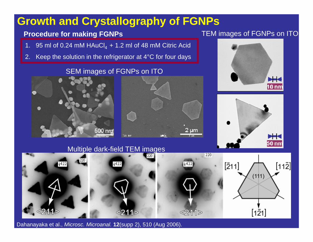
Growth and Crystallography of FGNPs
Multiple dark-field TEM images
1. 95 ml of 0.24 mM HAuCl4 + 1.2 ml of 48 mM Citric Acid
2. Keep the solution in the refrigerator at 4°C for four days
Procedure for making FGNPs
SEM images of FGNPs on ITO
TEM images of FGNPs on ITO
Dahanayaka et al., Microsc. Microanal. 12(supp 2), 510 (Aug 2006).

1D Postwetting Layer in InGaAs/GaAs(100) QD Chains
Z.M Wang et al. J. Appl. Phys. 99, 033705 (2006).

Defect Evaluation by Cross-sectional TEM

TI- FRAM Capacitor – Showing PZT Grains
• Fabrication Facilities & • Electron Microscopy
STEM showing PZT grains and grain boundaries. (Annular dark field detector & liq. N2 cooled sample)Grain Size Stats. Height = 64 ± 5 nm ; Width = 80 ± 25 nm
TiAlNTiAlN
IrIr
IrIr
TiAlNTiAlN
SiOSiO22/Si/Si33NN44
PZTPZT
TiAlNTiAlN
Ir/IrOIr/IrOxx
IrIr
TiAlNTiAlN
SiO2/Si3N4
PZT PZT
50 nm
500 nm
W PostW Post
W PostW PostEncapsulateEncapsulate
SiOSiO22
70 nm
x-SEM of Capacitor Stack
STEM image from Guoda Lian, TI
First TEM image showing PZT Grains.

F-RAM: NanoBeam Diffraction (NBD) Results
XT=0.4o
YT=2.3o
X:Y 0.952X is aY is c
XT=1.5o
YT=0.0o
X:Y 1.036X is cY is a
XT=0.0o
YT=0.8o
X:Y 1.00X is aY is a
XT=0.0o
YT=-1.5o
X:Y 0.957X is aY is c
100 nm
a[001]
[110]
X
Yc a c YT
XT
X
Y
[100] TetragonalDiffraction
Pattern

TEM - SEM NanoNet Projects at OU
PhysicsJohnson: Nanostructures Bumm: Flat Gold NanoParticlesMurphy: InSb Device FabricationSantos Defects in InSb structures ChemistryMao: Nano- Bio-materialsNelson SWNT functionalizationAMESaha: Nanocomposite materialsAltan: Nanocomposite materialsMerchan-Merchan: Nanocrystals
CBMEO'Rear: Surface Modification Mallinson: ZeolitesGrady: Nanoparticles for drug deliverySchmidtke: Bio-functionalized surfacesResasco: Carbon NanotubesECESluss: Silica shell NanoparticlesMcCann: IV-VI NanostructuresIndustrial EngineeringStarly: Electrospun BioscaffoldsOtherTeeters (TU) Nanobatteries and NanobasketsRoch (USAO): Polyaniline fibers

OU- OK NanoNet: Project Support (Regents)1. “Electrical and Thermal Conductivity of Carbon Nanotube-Polymer
Composites,” - Ford (OSU), Grady, Resasco
2. “Polymer Nanostructures on Solid Surfaces,” - Grady, Schmidtke, Striolo, Teeters (TU)
3. “Molecular Plasmonics on Gold Nanoparticles … ,” Halterman, Bumm
4. “Nanoparticle Sensors: Advanced Signaling Through PhotophysicalQuenching,” – Roberts (TU), Bumm, DiCesare (TU)
5. “DNA Packing into Nanoparticles,” Rybenkov, Zgurskaya
6. “Novel High Temperature Polymer Membranes for Fuel Cells,” Glatzhofer, Frech

OU- OK NanoNet: Facilities Tour• Fabrication Facilities & Electron Microscopy

OU- OK NanoNet: New Hire Support
AME: Mrinal Saha, Wilson Merchan-Merchan
ECE: Rui Yang, Matthew Kane
CBME: Alberto Striolo
Chemistry: Chuanbin Mao

OU- OK NanoNet: Summary• General Introduction to NanoResearch at OU
• Technical Support• Cleanroom / Electron Microscopy• ECE: MBE Position• CBME: XPS Position
• Project Support (Regents Match)Carbon Nanotube-Polymer CompositesPolymer Nanostructures on Solid SurfacesMolecular Plasmonics on Gold NanoparticlesNanoparticle SensorsDNA Packing into NanoparticlesPolymer Membranes for Fuel Cells
• Tour Fabrication Facilities & Electron Microscopy
• New Hire SupportAME: Saha, Merchan-Merchan ECE: Yang, KaneCBME: Striolo Chemistry: Mao