Origin of the surface recombination centers in ZnO...
24
Linköping University Post Print Origin of the surface recombination centers in ZnO nanorods arrays by X-ray photoelectron spectroscopy Li-Li Yang, Qingxiang Zhao, Magnus Willander, Xianjie Liu, Mats Fahlman and J H Yang N.B.: When citing this work, cite the original article. Original Publication: Li-Li Yang, Qingxiang Zhao, Magnus Willander, Xianjie Liu, Mats Fahlman and J H Yang, Origin of the surface recombination centers in ZnO nanorods arrays by X-ray photoelectron spectroscopy, 2010, APPLIED SURFACE SCIENCE, (256), 11, 3592-3597. http://dx.doi.org/10.1016/j.apsusc.2009.12.160 Copyright: Elsevier Science B.V., Amsterdam. http://www.elsevier.com/ Postprint available at: Linköping University Electronic Press http://urn.kb.se/resolve?urn=urn:nbn:se:liu:diva-54620
Transcript of Origin of the surface recombination centers in ZnO...

Linköping University Post Print
Origin of the surface recombination centers in
ZnO nanorods arrays by X-ray photoelectron
spectroscopy
Li-Li Yang, Qingxiang Zhao, Magnus Willander, Xianjie Liu, Mats Fahlman and J H Yang
N.B.: When citing this work, cite the original article.
Original Publication:
Li-Li Yang, Qingxiang Zhao, Magnus Willander, Xianjie Liu, Mats Fahlman and J H Yang,
Origin of the surface recombination centers in ZnO nanorods arrays by X-ray photoelectron
spectroscopy, 2010, APPLIED SURFACE SCIENCE, (256), 11, 3592-3597.
http://dx.doi.org/10.1016/j.apsusc.2009.12.160
Copyright: Elsevier Science B.V., Amsterdam.
http://www.elsevier.com/
Postprint available at: Linköping University Electronic Press
http://urn.kb.se/resolve?urn=urn:nbn:se:liu:diva-54620

1
Origin of the surface recombination centers in ZnO
nanorods arrays by X-ray photoelectron spectroscopy
L. L. Yang 1, 2*
, Q. X. Zhao 1
, M. Willander1, X. J. Liu
3, M. Fahlman
3 and J. H. Yang
2
1. Department of Science and Technology (ITN), Linköping University, SE-60174
Norrköping, Sweden
2. Institute of Condensed State Physics, Jilin Normal University, Siping, 136000,
People's Republic of China
3. Department of Physics, Chemistry and Biology, Linköping University, SE-581 83
Linköping, Sweden
Abstract
The surface composition of as-grown and annealed ZnO nanorods arrays (ZNAs)
grown by a two-steps chemical bath deposition method has been investigated by X-
ray photoelectron spectroscopy (XPS). XPS confirms the presence of OH bonds and
specific chemisorbed oxygen on the surface of ZNAs, as well as H bonds on
0)1(10 surfaces which has been first time observed in the XPS spectra. The
experimental results indicated that the OH and H bonds play the dominant role in
facilitating surface recombination but specific chemisorbed oxygen also likely affect
the surface recombination. Annealing can largely remove the OH and H bonds and
transform the composition of the other chemisorbed oxygen at the surface to more
closely resemble that of high temperature grown ZNAs, all of which suppresses
surface recombination according to time-resolved photoluminescence measurements.
Keywords: ZnO nanorods; Optical properties; Surface recombination; X-ray
photoelectron spectroscopy
* Author to whom any correspondence should be addressed.
E-mail: [email protected]

2
1. Introduction
Zinc oxide (ZnO) as one of the most important semiconductors has attracted
significant attention in recent years. Especially, quasi-one-dimensional ZnO
nanostructures (e.g. nanorods, nanowires, nanotubes and nanobelts) have been
considered highly potential for sensor application such as gas sensor [1-2] and
biosensor [3-5], and nanophotonic applications such as nanolasers [6–8], optical
waveguides [9–11], and light emitting diodes [12]. However, one of the significant
differences between nanostructures and an epilayer is the larger surface-to-volume
ratio of the former. This large surface-to-volume ratio can be an advantage for some
applications, for example sensor devices [1-5]. However, it can also be a problem in
other applications, for example, optoelectronic devices such as light emitting diodes
[12] and solar-cell [13-14] devices, since surface states are created within the band
gap region either because of surface inhomogeneities like nonstoichiometry or
because of the selective adsorption of foreign species in addition to the abrupt
termination of lattice periodicity. Such surface states will strongly influence the
electronic and optical properties at the semiconductor surfaces and interfaces since the
surface recombination rate may become dominating, resulting in a short carrier life
time [15-18]. The potential implications of these effects are especially noticeable in
the case of nanostructured materials. Therefore, to optimize devices based on ZnO
nanostructures, it is necessary to understand the surface recombination mechanisms
and explore effective way to control surface states. Furthermore, knowing surface
chemical origins in ZnO nanostructures are also essential for their applications in
sensor devices based on surface properties. For example, Z. K. Bai et al have reported
that the coverage of hydroxyl (OH) groups on the surface of tetrapod-shaped ZnO can
inhibit the ethanol adsorption [19-20], i.e. the high ratio of the coverage of OH group
can depress the high surface activity of the tetrapod-shaped ZnO sensor and block the
3
adsorption or reaction sites for the ethanol molecules, which lead to a smaller
consumption and sensing signal. Besides, as well known, the attraction or repulsion
action between chemical groups on the ZnO surface and detective molecule also
influence the sensitivity of ZnO sensor. Therefore, the investigation on the surface
recombination and chemical origins of surface recombination centers are significant
for the applications of ZnO nanostructures.
As we known, ZnO nanorods are a suitable material for the research on surface
recombination due to their large surface to volume ratio. Recently, we successfully
controlled the size of well-aligned ZnO nanorod arrays (ZNAs) from 40nm to 150nm
with the two-step chemical bath deposition (CBD) method [21, 22], i.e. by first spin
coating the substrate with a seed layer of ZnO nanoparticles and then using the CBD
growth. And we also investigated in detail the surface recombination of ZNAs with
different diameters by time-resolved photoluminescence measurement and revealed
that the surface recombination can be strongly suppressed by annealing at 500oC at
ambient conditions [23, 24]. We pointed out that the surface recombination maybe
originate from the functional groups absorbed by ZNAs surface during the chemical
reaction in the solution, which should be related to the elements such as carbon,
nitrogen and hydrogen, but we could not identify the origin of the surface
recombination due to the limitation of the used characterization techniques [24].
Although some groups have reported the possible functional groups attached in the
surface of the ZnO [25-35], so far, there are no investigations which try to build the
relationship between the chemical origin and surface recombination centers. On the
basis of the discussion in the first paragraph, we believe that the investigation on
identifying the chemical origin of surface recombination center is rather important
than just revealing the existence of surface recombination in the emission process,
because it will open to an effective way to control the surface recombination,utilize
4
the surface states for sensor application and efficiently enhance the properties of
optoelectronic devices based on ZnO nanostructures.
Therefore, in this paper, we utilized X-ray photoelectron spectroscopy (XPS) to
investigate the surface composition of as-grown ZNAs and ZNAs annealed in 500oC
for 1h in air atmosphere. The results clearly revealed the correlation between the
chemical origin and the surface recombination centers of ZNAs grown by CBD
method for the first time as far as we know.
2. Experimental
The ZNAs used in this investigation were grown on Si substrates by the CBD
method, which includes a two-steps process, i.e. a substrate treatment prior to the
CBD growth. The pre-treatment of the substrates, by coating the substrate with a
solution of zinc acetate dihydrate (Zn (OOCCH3)2·2H2O) dissolved in pure ethanol
with concentration of 5mM, was used to control the diameter of ZnO nanorods. In the
CBD growth, the aqueous solutions of zinc nitrate hexahydrate [Zn (NO3)2.6H2O,
99.9% purity] and methenamine (C6H12N4, 99.9% purity) were first prepared and
mixed together. The concentrations of both were fixed at 0.1M. The pre-treated Si
substrates were immersed into the aqueous solution and ZnO was grown at an
elevated temperature of 93oC. The more details of controllable preparation process of
ZNAs and some other controllable growth conditions can be found elsewhere [21-24].
To guarantee the comparability, a big piece of sample was cut into two parts. One was
used as as-grown sample, the other was post-growth thermal treated at 500oC for 1h in
air atmosphere and then quenched to room temperature by removal from the oven.
Scanning electron microscopy (SEM) pictures were recorded by using a JEOL
JSM-6301F. Transmission electron microscope (TEM) (200keV, JEM-2100HR, Japan)
was used to get the high resolution TEM (HRTEM) image and the selected-area

5
electron diffraction (SAED) pattern of samples. Time-resolved photoluminescence
(TRPL) was performed by using an excitation laser line from a frequency tripled
sapphire:Ti laser emitting at 266 nm with a 200 fs pulse width and a 80 MHz
repetition rate. The luminescence signal is dispersed by a 0.3 m monochromator and
time resolved by a streak camera. The spectral resolution is about 1 meV and the time
resolution is 7 ps. The measurements were done under weak excitation conditions (0.5
W/cm2) at 1.8 K. XPS measurements were performed using a Scienta® ESCA200
spectrometer in ultra-high vacuum (UHV) with a base pressure of 10−10
mbar. The
measurement chamber is equipped with a monochromatic Al (Kα) X-ray source
providing photon with hυ=1486.6 eV. The XPS experimental condition was set so
that the full width at half maximum (FWHM) of the clean Au 4f7/2 line was 0.65 eV.
All spectra were measured at a photoelectron take-off angle of 0º (normal emission)
and room temperature. The binding energies were obtained referenced to the Fermi
level with an error of ±0.1 eV.
3. Results and discussions
The SEM images of the as-grown and 500oC annealed ZNAs with 90 nm
diameters are shown in figure 1(a) and 1(b). In order to show the homogeneity of both
samples, only top-view SEM images are shown here. The length of nanorod is about 1
μm. From figure 1(a), it can be seen that the as-grown ZNAs are vertically aligned on
the Si (001) substrates. The hexagonally shaped nanorods uniformly cover the entire
Si substrate with high density. After 500oC post annealing, the morphology is almost
same with the as-grown ZNAs as shown in figure 1(b). The microstructure of the as-
grown ZNAs is further characterized by TEM and HRTEM, as shown in figure 1(c)
and 1(d). Figure 1(c) shows a low-magnification TEM image, confirming the
formation of the one-dimensional ZnO nanorods with 90nm diameter. The inset

6
SAED pattern further confirms that the as-grown ZNAs grow along the c-axis
direction since no splitting of the diffraction spots can be observed. Figure 1(d)
displays the typical HRTEM image of as-grown ZNAs. The HRTEM image clearly
reveals only the fringes with a lattice spacing of about 0.52 nm (equal to the lattice
constant c of ZnO), indicating that the ZnO nanorod is single crystalline in nature and
also further confirming that [0001] is the growth direction of the ZnO nanorods.
Figure 2 shows the effect of an annealing on the recombination decay at a
relative low temperature of 500 oC. As earlier demonstrated for Si epilayer [36-38],
the surface recombination can strongly influence the decay time. The excess minority
carriers via the near bandgap recombination exhibit a single exponential decay or a
biexponential decay, depending on whether the surface recombination is the major
recombination channel or not. Both decay curves exhibited a biexponential decay,
which demonstrated the existence of surface recombination [23-24]. To see it clearly,
the experimental curves in Fig.2 had been fitted by two exponential decays according
to the equation:
BS t
B
t
S eAeAtI //
)(
(1)
where I(t) represents the PL intensity as a function of time, while AS and AB are the
relative weights of the two exponential decays with time constants S and B,
respectively. The coloured lines in Fig.2 represent the fitting decay curves according
to Eq. (1). The fitting results show that the value of B is the same, 95 ps, for decay
curves from both as-grown and 500oC annealed ZNAs. We believe that this time
constant B represents an effective “bulk” exciton decay time in these two samples.
Then, S is assigned to the time constant which is related to surface recombination.
The detailed explanation about the assignments to B and S can be also found in
Ref.23, in which theoretical calculated results show a well consistency with these

7
assignments, especially for S. The value of S is 14 ps and 21 ps for the as-grown and
500oC annealed ZNAs, respectively, which clearly indicates that the decay constant
that arises from surface processes increases after annealing, i.e. the post-annealing at
500oC can suppress the surface recombination of ZNAs. For helping us discuss the
surface recombination centres later, the decay curve for ZnO nanorods grown at high
temperature (HT, 890oC) such as using the VLS growth (named as HT-ZNAs) is also
shown in Figure 2. The preparation of HT-ZNAs can be found in our previous work
[39]. In this case, the surface recombination can be neglected, and the decay curve
follows almost a single exponential decay.
We would like to point out that ZnO nanorods grown by CBD method actually
have two kinds of defects, i.e. surface defects and intrinsic defects (also called as deep
level defects)[23-24]. To further clearly distinguish the contribution from the surface
defects and intrinsic defects, for the prolonged decay time after 500oC annealing, we
also investigated the effect of annealing temperature on the optical properties of ZnO
nanorods [24]. In Ref. [24], we utilized the Resonant Raman spectroscopy to monitor
the change of surface defects and deep level defects in the CBD grown ZnO nanorods
under thermal treatment from 500°C to 700°C. By correlating the Raman
measurements, PL measurements and time-resolved PL measurements, we proved
that the surface defects had a significant contribution to the observed strong Raman
intensity of 1LO and 2LO (A1-LO mode) in the CBD as-grown samples. The results
also clearly indicated that the surface defects played a significant role in the as-grown
sample and 500oC annealing treatment can successfully release some part of the
surface defects. Therefore, it is not hard to see that the surface recombination centers
can be successfully revealed through comparing the surface composition of as-grown
and 500oC annealed ZNAs.

8
XPS was used to investigate the surface composition of as-grown and 500oC
annealed ZNAs. Figure 3 shows the XPS survey spectra from as-grown and annealed
ZNAs, in which all of the peaks can be only ascribed to Zn, O, and C elements as
labeled in Figure 3b [25]. It indicated that there were no other impurities observed in
both samples. We would like to mention that, in all the XPS spectra of ZNAs, the
binding energies have been calibrated by taking the carbon C1s peak (285.0 eV) as
reference.
The deconvolutions of the XPS spectra for the O1s core level line from the as-
grown and annealed ZNAs are shown in Figure 4(a) and 4(b), respectively. For all
XPS spectra in the paper, the open circles denote the experimental data, red solid line
represents the fitting curves and the deconvoluted individual peaks are depicted by
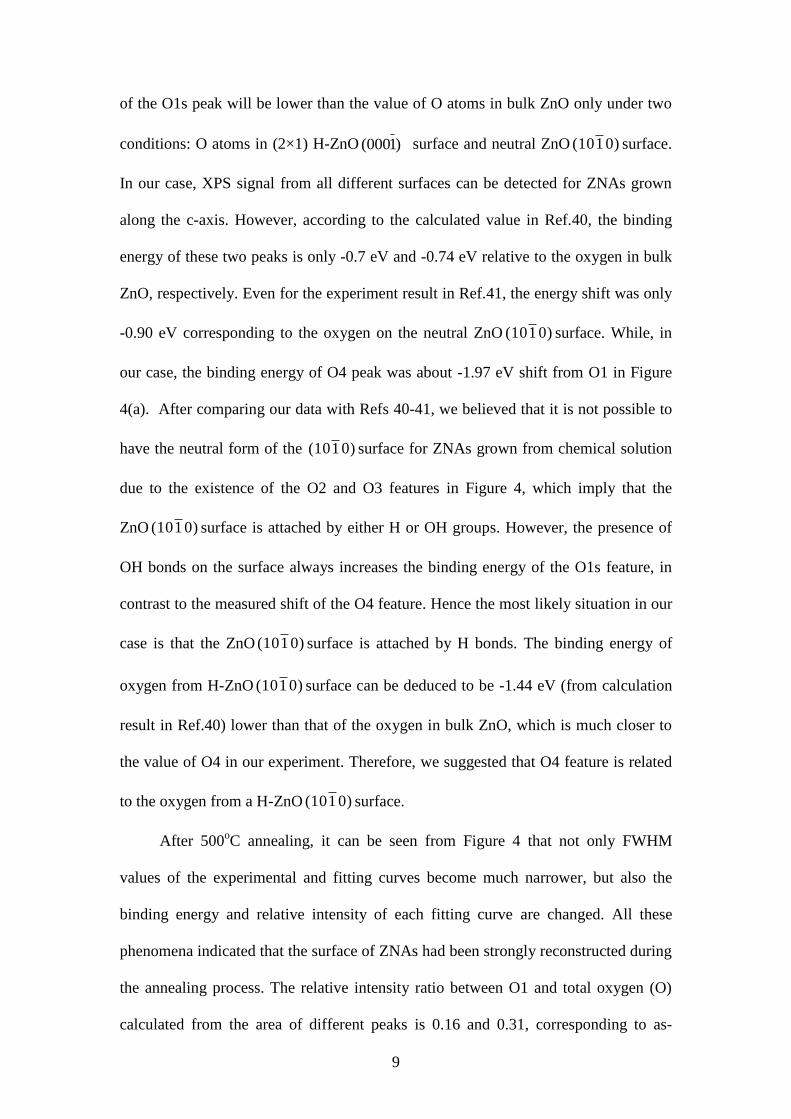
green lines. In Figure 4(a), the deconvolutions show the presence of four different
O1s peaks in the as-grown ZNAs. The peak centered at 530.35±0.3 eV (O1) is
associated to the O2-
ion in the wurzite structure surrounded by the Zn atoms with
their full complement of nearest-neighbor O2-
ions [26-35]. The peak at 531.54±0.3
eV (O2) is attributed to the presence of OH bonds, i.e. ZnO(OH) [28-32]. The binding
energy peak at 532.87±0.3 eV (O3) can be ascribed to the specific chemisorbed
oxygen, such as -CO3, adsorbed O2, or adsorbed H2O [26-35]. Usually, only these
three peaks can be extracted from O1s XPS spectrum. But in our case, we observe
another peak located at 528.38±0.3 eV (O4). K. Kotsis and V. Staemmler have
reported ab initio calculation of the O1s spectra of ZnO and Zn oxo compounds [40],
where different binding energy values of O1s were calculated corresponding to
different O atoms on the polar O-terminated ZnO (0001) : adsorption of H atoms (i.e.
H-ZnO (0001) ) with (2×1) and (1×1) surface structure and also the O atoms on the
neutral ZnO 0)1(10 surface. According to their calculation results, the binding energy
9
of the O1s peak will be lower than the value of O atoms in bulk ZnO only under two
conditions: O atoms in (2×1) H-ZnO (0001) surface and neutral ZnO 0)1(10 surface.
In our case, XPS signal from all different surfaces can be detected for ZNAs grown
along the c-axis. However, according to the calculated value in Ref.40, the binding
energy of these two peaks is only -0.7 eV and -0.74 eV relative to the oxygen in bulk
ZnO, respectively. Even for the experiment result in Ref.41, the energy shift was only
-0.90 eV corresponding to the oxygen on the neutral ZnO 0)1(10 surface. While, in
our case, the binding energy of O4 peak was about -1.97 eV shift from O1 in Figure
4(a). After comparing our data with Refs 40-41, we believed that it is not possible to
have the neutral form of the 0)1(10 surface for ZNAs grown from chemical solution
due to the existence of the O2 and O3 features in Figure 4, which imply that the
ZnO 0)1(10 surface is attached by either H or OH groups. However, the presence of
OH bonds on the surface always increases the binding energy of the O1s feature, in
contrast to the measured shift of the O4 feature. Hence the most likely situation in our
case is that the ZnO 0)1(10 surface is attached by H bonds. The binding energy of
oxygen from H-ZnO 0)1(10 surface can be deduced to be -1.44 eV (from calculation
result in Ref.40) lower than that of the oxygen in bulk ZnO, which is much closer to
the value of O4 in our experiment. Therefore, we suggested that O4 feature is related
to the oxygen from a H-ZnO 0)1(10 surface.
After 500oC annealing, it can be seen from Figure 4 that not only FWHM
values of the experimental and fitting curves become much narrower, but also the
binding energy and relative intensity of each fitting curve are changed. All these
phenomena indicated that the surface of ZNAs had been strongly reconstructed during
the annealing process. The relative intensity ratio between O1 and total oxygen (O)
calculated from the area of different peaks is 0.16 and 0.31, corresponding to as-
10
grown and annealed sample respectively. This indicates that the crystallization of
ZNAs becomes much better through the annealing process. It is worth to notice that,
in comparison with Figure 4(a), the most dramatic change in Figure 4(b) (after
annealing) is that the O4 peak totally disappeared and the O2 peak is strongly
suppressed. We can thus suggest that O4 and O2 play significant roles in the surface
recombination of ZNAs, and we propose that O4 and O2 correspond to the presence
of H bonds on 0)1(10 surface and OH on the surface of ZNAs respectively.
We would like to point out here that some oxygen species may not be
detectable due to their less concentration than the detection limit of XPS equipment.
Although we can not deny their possible contributions to the surface recombination,
we can only explain the results which we have observed from the available
experimental techniques. We hope our results will stimulate and promote the further
investigations in order to definitely conclude the origin of the surface defects which
are involved in the recombination.
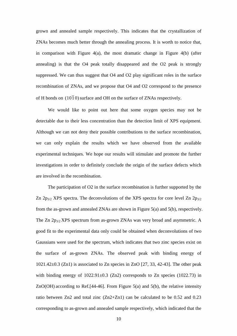
The participation of O2 in the surface recombination is further supported by the
Zn 2p3/2 XPS spectra. The deconvolutions of the XPS spectra for core level Zn 2p3/2
from the as-grown and annealed ZNAs are shown in Figure 5(a) and 5(b), respectively.
The Zn 2p3/2 XPS spectrum from as-grown ZNAs was very broad and asymmetric. A
good fit to the experimental data only could be obtained when deconvolutions of two
Gaussians were used for the spectrum, which indicates that two zinc species exist on
the surface of as-grown ZNAs. The observed peak with binding energy of
1021.42±0.3 (Zn1) is associated to Zn species in ZnO [27, 33, 42-43]. The other peak
with binding energy of 1022.91±0.3 (Zn2) corresponds to Zn species (1022.73) in
ZnO(OH) according to Ref.[44-46]. From Figure 5(a) and 5(b), the relative intensity
ratio between Zn2 and total zinc (Zn2+Zn1) can be calculated to be 0.52 and 0.23
corresponding to as-grown and annealed sample respectively, which indicated that the

11
intensity of Zn2 peak was sharply suppressed after 500oC annealing. This
phenomenon further testified that presence of OH bonds as an origin of surface
recombination, in excellent agreement with the results from O1s XPS spectra.
We also found in Figure 4(a) and 4(b) that the component O3 ascribed to
chemisorbed oxygen can not be removed by annealing even at temperatures as high as
500oC. As mentioned before, O3 is usually ascribed to the specific chemisorbed
oxygen, such as -CO3, adsorbed O2 or adsorbed H2O [26-35]. In Figure 4 it can be
observed that the binding energy of the O3 peak shifts from 532.87±0.3 eV to 532.28
±0.3 eV and the FWHM also decreased from 2.01 eV to 1.60 eV after annealing. The
peak position of O3 can vary depending on adsorbant, e.g. from 532.25 eV [29] to
533.21 eV [35], and the exact energy position depended on the relative ratio between
the different components involved in O3 peak due to the growth process [26-35].
Therefore, the large shift of the O3 position in Figure 4 indicates a change of the
relative contribution to the O3 peak from the different adsorbant components, which
might also cause a change in the surface recombination. In order to determine the
effects of O3 on the surface recombination, we have to look back on Figure 2. From
Figure 2, we can observe that although the decay time for 500oC annealed sample is
prolonged compared with the as-grown sample, it still does not totally change into an
exponential one like that of the HT-ZNAs, which suggests that although the surface
recombination is strongly suppressed by the annealing process, it is still non-
negligible in the photoluminescence process. A possible origin for the remnant
surface recombination after annealing could thus be O2 that has not totally released
and possibly O3 as well.
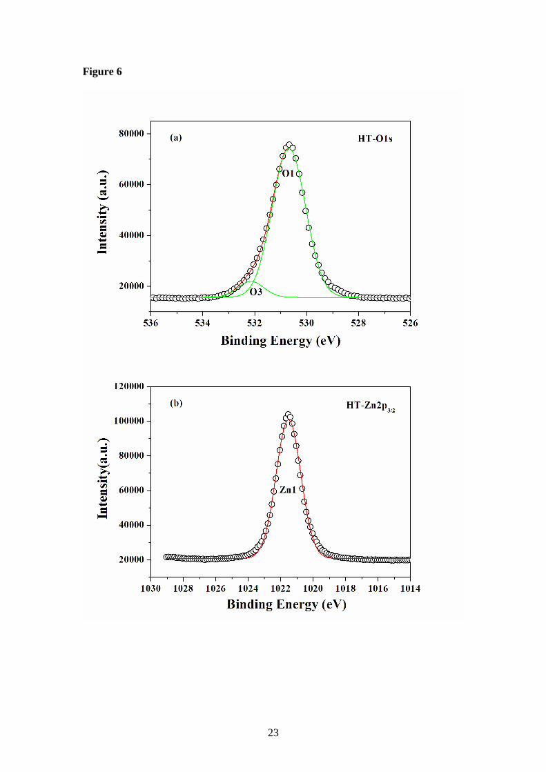
In order to further investigate the contribution from O3 to the surface
recombination, O 1s and Zn 2p3/2 XPS spectra from HT-ZNAs are shown in Figure 6.
From Figure 6(a), we depict the best fit obtained from a deconvolution of two

12
Gaussians. The two peaks centered at the 530.68±0.3 eV and 532.15±0.3 eV
correspond to O1 and O3 respectively. From Figure 6(b), only one component of Zn1
is enough to fit the experiment curve. All these results further testify that the OH and
H bonds on the surface are chemical origins of surface recombination in ZNAs grown
by CBD method. In addition, from Figure 6(a), it can also be observed that O1 is the
dominant part of the whole signal of O1s unlike in Figure 4. The relative intensity
ratio of O3/O is only 0.075, in fact, so the effect of O3 can be neglected in the
photoluminescence process for the HT-ZNAs. The O3 feature is always the dominant
component in the whole signal of O1s in the as-grown and annealed ZNAs grown by
CBD method, however, as shown in Figure 4. Hence, we believe that the O3
contribution to the photoluminescence process can not be neglected for such samples
and specific chemisorbed oxygen likely contributes to surface recombination.
Moreover, in comparison with the annealed sample in Figure 4(b), the binding energy
of the O3 feature in HT-ZNAs in Figure 6(a) is shifted to lower energy. Note that the
binding energy of O3 in the annealed sample also is shifted to lower energy compared
to the as-grown sample as mentioned before. This suggests that the annealing process
changes the composition of the chemisorbed oxygen species to something more
closely related to the case of HT-ZNAs, which in turn may have a lesser contribution
to the surface recombination.
4. Conclusion
In this paper, we have performed an XPS investigation on the surface of as-
grown and annealed ZNAs. We found that surface recombination correlates to the
presence of OH bonds and specific chemisorbed oxygen on the surface of ZNAs, and
H bonds on 0)1(10 surface. The experimental results suggest that OH and H bonds
play the dominant role in the surface recombination but specific chemisorbed oxygen
also likely affect the surface recombination. Annealing can largely remove the OH

13
and H bonds and transform the composition of the other chemisorbed oxygen at the
surface to more closely resemble that of high temperature grown ZNAs, all of which
corresponds to a suppression of surface recombination according to time-resolved
photoluminescence measurements. We believe these results can enlighten the other
researchers to explore effective ways to suppress the surface recombination, which
will prompt the practical application of ZNAs in the future, and the results can also
further stimulate theoretical investigation of the surface chemical clusters.
Acknowledgements
The authors would like to acknowledge financial support for this work from the
Swedish Research Council (VR) and financial support through Swedish Research
Links via VR. L.L. Yang would also like to acknowledge financial support from
National Nature Science Foundation of China (NNSFC, No.60878039 and 60778040),
program for the development of Science and Technology of Jilin province (Item No.
20090140) and the Eleventh Five-Year Program for Science and Technology of
Education Department of Jilin Province (Item No. 20080156).

14
References:
[1] H. Zhang, J. B. Wu, C. X. Zhai, N. Du, X. Y. Ma and D. R. Yang,
Nanotechnology 18 (2007) 455604.
[2] L. Liao, H. B. Lu, J. C. Li, C. Liu, D. J. Fu and Y. L. Liu, Appl. Phys. Lett. 91
(2007) 173110.
[3] A. Wei, X. W. Sun, J. X. Wang, Y. Lei, X. P. Cai, C. M. Li, Z. L. Dong, W.
Huang, Appl. Phys. Lett. 89 (2006) 123902.
[4] A. Umar, M. M. Rahman, S. H. Kim, Y. B. Hahn, J. Nanoscience and
Nanotechnology 8 (2008) 3216.
[5] S. Al-Hill, M. Willander, Nanotechnology 20 (2009) 175103.
[6] M. H. Huang, S. Mao, H. Feick, H. Yan, Y. Wu, H. Kind, E. Weber, R. Russo
and P. Yang, Science 292 (2001) 1897.
[7] J. C. Johnson, H-J Choi, K. P. Knutsen, R. D. Schaller, P. Yang and R. J.
Saykally, Nat. Mater. 1 (2002) 106.
[8] X. Duan, Y. Huang, R. Agarwal and C. M. Lieber, Nature (London) 421 (2003)
241.
[9] M. Law, D. J. Sirbuly, J. C. Johnson, J. Goldberger, R. J. Saykally and P. Yang
Science 305 (2004) 1269.
[10] C. J. Barrelet, A. B. Greytak and C. M. Lieber, Nano Lett. 4 (2004) 1981.
[11] A. B. Greytak, C. J. Barrelet, Y. Li and C. M. Lieber, Appl. Phys. Lett. 87 (2005)
151103.
[12] M. Willander, L. L. Yang, A. Wadeasa, S. U. Ali, M. H. Asif, Q. X. Zhao and O.
Nur, J. Mater. Chem. 19 (2009) 1006.
[13] Y. Y. Lin, Y. Y. Lee, L.W. Chang, J. J. Wu, C.W. Chen, Appl. Phys. Lett. 94
(2009) 063308.
[14] Z. L. S. Seow, A. S. W. Wong, V. Thavasi, R. Jose, S. Ramakrishna, G. W.
Ho ,Nanotechnology 20 (2009) 045604.

15
[15] S. C. Erwin, L. Zu, M. I. Haftel, A. L. Efros, T. A. Kennedy, D. J. Norris, Nature
436 (2005) 91.
[16] P. Zhang, E. Tevaarwerk, B. Park, D. E. Savage, G. K. Celler, I. Knezevic, P. G.
Evans, M. A. Erikkson, M. G. Lagally, Nature 439 (2006) 703.
[17] J. J. Boland, Nature 439 (2006) 671.
[18] Q. Wan, T. H. Wang, J. C. Zhao, Appl. Phys. Lett. 87 (2005) 083105.
[19] Z. K. Bai, C. S. Xie, M. L. Hu, S. P. Zhang, D. W. Zeng, Mater. Science and
Engineering B 149 (2008) 12.
[20] W. Schmid, N. Bârsan, U. Weimar, Sens. Actuator B 89 (2003) 232.
[21] L. L. Yang, Q. X. Zhao, M. Willander, J. Alloys and Compounds 469 (2009) 623.
[22] L. L. Yang, Q. X. Zhao, M. Willander, J. H. Yang J. Crystal Growth 311 (2009)
1046 .
[23] Q. X. Zhao, L. L. Yang, M. Willander, B. E. Sernelius and P. O. Holtz, J. Appl.
Phys. 104 (2008) 073526.
[24] L. L. Yang, Q. X. Zhao, M. Willander, J. H. Yang and I. Ivanov, J. Appl. Phys.
105 (2009) 053503.
[25] Seung Yong Bae, Hyun Chul Choi, Chan Woong Na, and Jeunghee Park, Appl.
Phys. Lett. 86 (2005) 033102.
[26] L. J. Meng, C. P. Moreira, and M. P. d. Santos, Appl. Surf. Sci. 78 (1994) 57.
[27] Y. F. Lu, H. Q. Ni, Z. H. Mai, and Z. M. Ren, J. Appl. Phys. 88 (2000) 498.
[28] E. De la Rosa, S. Seplveda-Guzman, B. Reeja-Jayan, A. Torres, P. Salas, N.
Elizondo, and M. Jose Yacaman, J. Phys. Chem. C 111 (2007) 8489.
[29] H.H. Wang, S.H. Baek, J.J. Song, J.H Lee and S.W. Lim, Nanotechnology 19
(2008) 075607.
[30] L. J. Meng, C. P. Moreira de Sa and M. P. Dos Santos, Appl.Surf. Sci. 78 (1994)
57.

16
[31] N. Boulares, K. Guergouri, R. Zouaghi, N. Tabet, A. Lusson, F. Sibieude and C.
Monty, Phys. Status Solidi A 201–210 (2004) 2319.
[32] A. Toumiat, S. Achour, A. Harabi, N. Tabet, M. Boumaour and M. Maallemi,
Nanotechnology 17 (2006) 658.
[33] M. Chen, X. Wang, Y. H. Yu, Z. L. Pei, X. D. Bai, C. Sun, R. F. Huang, L. S.
Wen, Appl. Surf. Sci. 158 (2000) 134.
[34] B. J. Coppa, R. F. Davis, R. J. Nemanich, Appl. Phys. Lett. 82 (2003) 400.
[35] H. H. Wang, C. S. Xie, Physica E 40, 2724(2008).
[36] K. L. Luke and L. J. Cheng, J. Appl. Phys. 61, 2282 (1987).
[37] A. Buczkowski, Z.J. Radzimski, G.A. Rozgonyi and F. Shimura, J. Appl. Phys.
69, 6495 (1991).
[38] K. Thölmann, M. Yamaguchi, A. Yahata and H. Ohashi, Jpn. J. Appl. Phys. 32, 1
(1993).
[39] Q.X. Zhao, P. Klason and M. Willander, Applied Phys. A 88 (2007) 27.
[40] Konstantinos Kotsis and Volker Staemmler, Phys. Chem. Chem. Phys. 8 (2006)
1490.
[41] St.Gil Girol, PhD thesis, Ruhr-Universität, Bochum, 2004.
[42] N. S. Ramgir, D. J. Late, A. B. Bhise, M. A. More, I. S. Mulla, D. S. Joag, and K.
Vijayamohanan, J. Phys. Chem. B 110 (2006) 18236.
[43] C.Y. Leunga, A.B. Djurišić, Y.H. Leung, L. Ding, C.L. Yang, W.K. Ge, J.
Crystal Growth 290 (2006) 131.
[44] B. V. Crist, Handbooks of Monochromatic XPS spectra - Vol.2 - Commercially
Pure Binary Oxides, XPS International, Inc., 1999, PP820.
[45] R. Umebayashi, N. Akao, N. Hara, K. Sugimoto, J. Electrochemical Society,150
(2003) B295.
[46] C. Pettenkofer, U. Meier, Appl. Surf. Sci. 252 (2005) 1139.

17
Figure captions:
Figure 1. (a) and (b) SEM images for as-grown and 500oC annealed ZNAs; (c) TEM
image of single as-grown ZnO nanorod, the inset is the corresponding SAED pattern;
(d) HRTEM of as-grown ZnO nanorod.
Figure 2. Decay curves from as-grown and annealed ZNAs. Decay curve from high-
temperature (890oC) as-grown sample was also shown at here for comparison. The
decays were measured at 1.8 K. The colour lines are fitted according to Eq. (1).
Figure 3. XPS survey spectra of as-grown ZNAs (a) and annealed ZNAs (b), where
the labels indicated the origins of the corresponding peaks.
Figure 4. (a) O1s XPS spectra of as-grown ZNAs where four components (green
curves) were used to deconvolute the experimental peak, as labeled by O1, O2, O3
and O4. (b) O1s XPS spectra of ZNAs after 500oC annealing. Only O1, O2 and O3
components were extracted from the experimental curve.
Figure 5. Zn 2p3/2 XPS spectra of as-grown ZNAs (a) and annealed ZNAs (b), where
two components (green curves) were used to deconvolute the experimental peak, as
labeled by Zn1 and Zn2.
Figure 6. (a) O 1s XPS spectra of high temperature (890oC) grown ZNAs, where only
O1 and O3 components were extracted from the experimental curve (green curves). (b)
Zn 2p3/2 XPS spectra of high temperature (890oC) grown ZNAs, one component of
Zn1 is enough to fit the experiment curve.

18
Figure1

19
Figure 2

20
Figure 3

21
Figure 4

22
Figure 5
23
Figure 6