Organic Nanophotonics for Low-Cost Biosensing · Organic Nanophotonics for Low-Cost Biosensing ......
18
A5.5 Lemmer 1 Subproject A5.5 Organic Nanophotonics for Low-Cost Biosensing Principal Investigators: Uli Lemmer CFN-Financed Scientists: One Ph.D. position since March 2007 Further Scientists: Sönke Klinkhammer, Christoph Vannahme, Thomas Woggon, Jan Brückner, Carsten Eschenbaum, Uwe Bog, Birgit Rudat, Dr. Timo Mappes Lichttechnisches Institut Karlsruher Institut für Technologie (KIT)
Transcript of Organic Nanophotonics for Low-Cost Biosensing · Organic Nanophotonics for Low-Cost Biosensing ......

A5.5 Lemmer
1
Subproject A5.5
Organic Nanophotonics for Low-Cost Biosensing Principal Investigators: Uli Lemmer CFN-Financed Scientists: One Ph.D. position since March 2007 Further Scientists: Sönke Klinkhammer, Christoph Vannahme, Thomas Woggon, Jan Brückner, Carsten Eschenbaum, Uwe Bog, Birgit Rudat, Dr. Timo Mappes Lichttechnisches Institut Karlsruher Institut für Technologie (KIT)

A5.5 Lemmer
2
Organic Nanophotonics for Low-Cost Biosensing Introduction and Summary The field of organic optoelectronic devices is steadily growing [1,2]. One of the most prominent applications is the use of organic light-emitting diodes (OLEDs) for example in small displays in mobile phones, MP3-audio players or even TV displays. Other research areas are organic solar cells and photodetectors being of great interest for large-area, low-cost applications [3, 4, 5]. Organic devices can be fabricated by relatively low-cost manufacturing methods on a wide range of different substrates [6]. Organic lasers are a special type of organic light-emitting devices [7]. In contrast to OLEDs, these devices emit a highly directional, monochromatic beam of light. By using different materials the whole visible wavelength range can be covered by the laser emission [8, 9, 10, 11]. These lasers can also be fabricated by low-cost methods [12, 13] rendering them interesting for an application in optical sensor systems. In the last years the vision of a complete analysis system integrated “on a chip”, a so called lab-on-chip (LOC), attracts an increasing number of users and research groups [14, 15, 16, 17, 18]. Possible applications for such systems are in the areas of medicine, drug discovery and environmental monitoring. Instead of shipping a sample for an analysis to a central laboratory one could use such small, portable systems for point-of-care diagnostics [19, 20]. Optical detection schemes such as laser induced fluorescence, absorbance detection, or evanescent field sensing are commonly used approaches in sensor systems. Today, these techniques are usually based on external laser sources and complicated coupling optics being bulky and expensive. The monolithic integration of nanophotonic laser light sources onto the chip will result in small, portable and far more flexible systems [21, 22, 23, 24, A5.5:9]. 1. Organic Semiconductor Distributed Feedback Lasers 1.1. Resonator structure Among different approaches for the resonator design [25, 26] the distributed feedback (DFB) resonator scheme is one of the most promising ones for organic lasers due to its rather simple and efficient design. Typically, the organic DFB laser consists of a thin–film active material that is deposited on top of a periodically corrugated substrate. The active material is optically pumped, for example by an external pulsed UV laser. The layers sequence forms a slab waveguide (thickness < 400 nm) confining the optical wave in the substrate plane. The so called distributed feedback mechanism of the laser relies on Bragg scattering induced by a periodic modulation of the refractive index due to the surface corrugations (gratings) of the substrate. The lasing wavelength las of a DFB laser can be estimated using a modified version of Bragg’s formula las = 2 neff /m. (1) The effective refractive index of the guided mode is neff, the Bragg order which provides the necessary feedback is m and the grating period of the structure is given by . As a part of this project the lasing mechanisms in organic photonic crystal lasers with two-dimensional distributed feedback were investigated experimentally as well as theoretically [A5.5:2, A5.5:3] in collaboration with Prof. Dr. Kurt Busch’s group of the Institut für Theoretische Festkörperphysik at the KIT.
A5.5 Lemmer
3
1.2. Organic semiconductor energy transfer systems as active laser medium Organic semiconductors have attracted a lot of attention as active materials in the recent years. Their broad spectral emission range in the visible, their high efficiency combined with the ease of fabrication and low costs make them ideal candidates as gain materials in broadband laser sources. Organic semiconductor materials are generally available as conjugated polymers [27,28] or so-called small molecules [29], but also other classes of molecules like spiro-linked compounds [30] or conjugated dendrimers [31] have been demonstrated in laser devices . Material systems with a large spectral gap between the absorption of the excitation light and the laser emission are of particular interest for organic semiconductor lasers. This reduces the self-absorption of the emission leading to a more efficient lasing operation. Such a system can be fabricated by molecular doping of a host material thus forming a so-called guest-host material. A very well studied efficient material complex is the organic semiconductor tris(8-hydroxyquinoline) aluminum (Alq3) and doped with laser dye 4-dicyanmethylene-2-methyl-6-(p-dimethylaminostyryl)-4H-pyran (DCM). The exciting radiation is absorbed in the host material. The absorbed energy is then transferred by a radiationless process to the guest material lifting it into an electronically excited state (see Fig. 1). The predominantly utilized energy transfer mechanism for organic semiconductor lasers is the so called Förster resonance energy transfer [8]. This process is based on a dipole-dipole interaction and therefore requires a spectral overlap of the donor’s emission with the acceptor’s absorption. The effective radius of this process can be up to 10 nm.
~~~~~~~~~
photon energytransfer
Alq3 DCM
Fig. 1: Energy transfer in dye doped organic semiconductors. 1.3 Optical pumping schemes There are several approaches for optically pumping an organic semiconductor laser. The high absorbance of the pump light in the laser material is a basic requirement. Additionally, short pulses and a small focus are advantageous. Depending on the material the pulse duration has a critical influence on the threshold where lasing can be observed. This condition depends on the ratio of the fluorescence lifetime and the pump pulse duration [32]. Due to their short pulses and high energy densities, diode pumped solid state (DPSS) lasers were the first compact laser sources used for pumping organic semiconductor lasers [10]. With steady advances in developing low threshold organic lasers [A5.5:4,A5.5:10, 34] we were able to present a gallium nitride laser diode-pumped organic laser in 2006 [35, A.5.5:11]. In 2008, the first organic laser pumped by a blue light emitting diode was demonstrated [36]. Furthermore, we successfully demonstrated free-space pumping of organic semiconductor microcone lasers with a low-cost laser diode [37].

A5.5 Lemmer
4
1.4 Prospects for organic laser diodes With various optoelectronic components based on organic semiconductors being implemented successfully during the last decade, an organic laser diode device has become of particular interest. However, it could not be realized so far. Electrically pumped organic lasers are expected to provide numerous advantages over their inorganic counterparts like tunability over the whole visible spectrum and the promise of low-cost fabrication. The implementation of such a device seems to be straight forward. Electrodes are put on both sides of the slab waveguide formed by the organic laser material to inject charge carriers. The problem, however, is the strong optical loss which is introduced by coating the waveguide with a metal layer or even with a transparent metal oxide layer like indium tin oxide (ITO). To deal with this problem the thickness of the organic layer can be increased in order to minimize the overlap of the guided mode with the absorbing electrodes. However, this results in very high operation voltages of the device. Although high current densities for thin-film devices can be achieved without damaging the organic layer [38, 39, 40], neither an electrically pumped organic laser nor an electrically pumped organic amplifier has been shown yet. Our numerical simulations show, that the main reason for this behavior is the rising charge carrier density which causes additional losses like bimolecular annihilation, induced absorption by polarons and triplet excitons, and field-induced exciton dissociation [41, A5.5:5, A5.5:7]. 2. Fabrication There are basically two methods to realize DFB resonator gratings: either the lower or the upper active layer boundary has to be patterned with the requested topography of the distributed feedback grating. As shown in Fig. 2, this may be achieved either by direct patterning of the active laser material or by structuring the substrate beneath the active layer. The quality of the resonator structure affects threshold and efficiency of the laser. For patterning of the active layer photoisomerization [42], direct embossing [43, 44] or direct laser interference ablation can be used.
Laser material
Substrate
Laser material
Substrate
Laser material
Substrate Fig. 2: Different methods to pattern the active material layer of an organic semiconductor laser.
Patterning of the substrate might be advantageous since this process is independent of the properties of the active material. Hence, most fabrication techniques for organic semiconductor lasers are based on structured substrates. To fabricate DFB resonators of first and second order for lasers in the visible range, grating periods of 100-400 nm are required [45]. In the following paragraph an overview of the different fabrication methods of DFB resonators for organic semiconductor lasers is given. Fig. 3 schematically illustrates the possible nanopatterning processes. There are three main process chains that lead to a DFB resonator grating substrate. Each process chain includes structuring of a master substrate. In the first one (1) this master is directly used as laser substrate. However, the fabrication of a master substrate is expensive and time-consuming, thus this method is only used for prototyping. A second process chain (2) uses the replication of the master substrate. Different methods allow multiple

A5.5 Lemmer
5
replications with the master substrate used as a molding tool. However, the master itself may be damaged during the process. This is avoided by introducing the fabrication of a replication tool (3) which can be optimized for long durability. Thus, the latter process chain is best suited for commercial applications. The master substrate can be fabricated by serial or parallel processes. Serial processes like electron beam lithography or direct laser writing allow for highest freedom in design of the structures. In comparison parallel processes like laser interference lithography or ablation are fast and applicable to large areas. In the following we will describe the most important fabrication methods which have been elaborated in the course of the project:
Master grating fabrication
Serial methods- Electron beam lithography- Direct laser writing
Parallel methods- Laser interference lithography- Laser interference ablation- Self-assembly
Tool fabrication
- Molding tool (hard/soft)- Lithography masks
Replication techniques
Imprinting- Hot embossing- UV-Nanoimprint-Lithography- Microcontact printing
Casting- Replica molding(hard/soft)
Lithography- Photolithography
Patterned substrate
1
2
3
Fig. 3: Overview of DFB resonator fabrication methods.
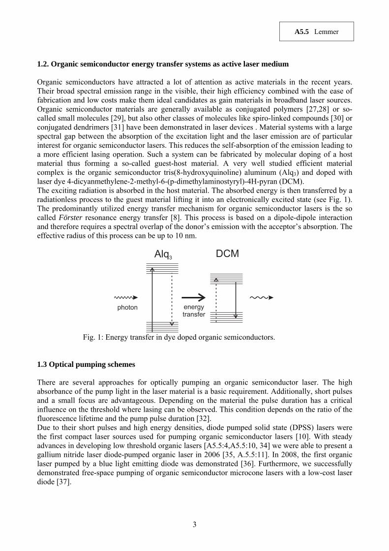
2.1 Master fabrication by laser interference lithography Laser interference lithography (LIL) is one of the most important techniques for the fabrication of periodic structures. In contrast to electron beam lithography it is possible to quickly pattern large areas with this technique. Although the basic principle behind LIL is quite simple, the realization of large area and high quality structures is a difficult task [A5.5:2, 46]. A scheme of our LIL setup is shown in Fig. 4. A laser beam is split into two single beams which are directed onto a photosensitive resist. This results in a locally varying exposure dosage, leaving a periodic structure after developing the resist. The interference pattern grating constant Λ can be calculated by Λ=λ/(2sinα), with the angle α between the substrate normal and the laser beam. Therefore the lower limit of the grating constant is half of the laser wavelength λ. In case of the commonly used argon ion laser emitting at 364 nm this means theoretically a minimal lattice period of 182 nm. A long coherence length of the laser is needed in order to realize a substrate sized interference pattern. Additionally, a mechanically stable
A5.5 Lemmer
6
optical setup is obligatory. As a rough estimation the displacement of the interference pattern should be lower than 1/10 of the period during exposure. After developing the structure, it can either be used directly as a laser resonator or transferred into another material. As the substrate can be rotated by 90 or 60 degrees, square and triangular lattices can also be patterned with LIL using multiple exposures.
Sample
Laser�
Su
bstr
ate
Ph
oto
resis
t
Fig. 4: Schematic experimental setup for laser interference lithography. The inset shows the pattern created by the interfering beams.
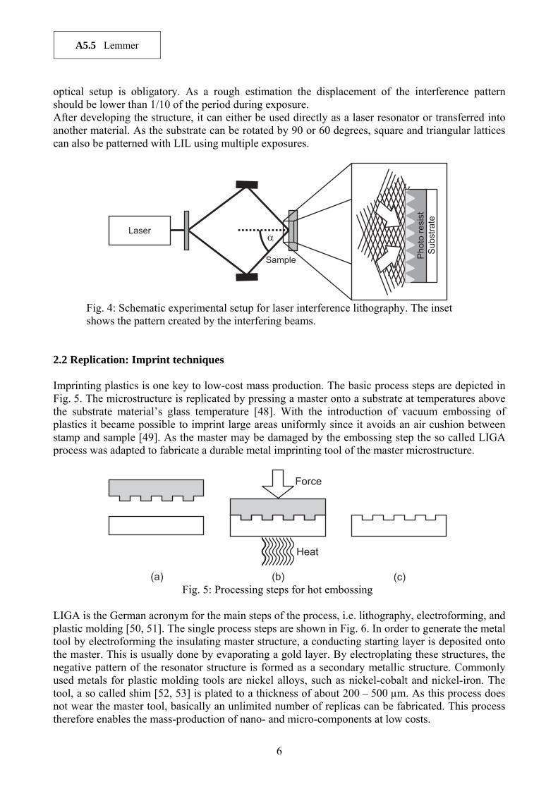
2.2 Replication: Imprint techniques Imprinting plastics is one key to low-cost mass production. The basic process steps are depicted in Fig. 5. The microstructure is replicated by pressing a master onto a substrate at temperatures above the substrate material’s glass temperature [48]. With the introduction of vacuum embossing of plastics it became possible to imprint large areas uniformly since it avoids an air cushion between stamp and sample [49]. As the master may be damaged by the embossing step the so called LIGA process was adapted to fabricate a durable metal imprinting tool of the master microstructure.
(a) (b) (c)
Force
Heat
Fig. 5: Processing steps for hot embossing
LIGA is the German acronym for the main steps of the process, i.e. lithography, electroforming, and plastic molding [50, 51]. The single process steps are shown in Fig. 6. In order to generate the metal tool by electroforming the insulating master structure, a conducting starting layer is deposited onto the master. This is usually done by evaporating a gold layer. By electroplating these structures, the negative pattern of the resonator structure is formed as a secondary metallic structure. Commonly used metals for plastic molding tools are nickel alloys, such as nickel-cobalt and nickel-iron. The tool, a so called shim [52, 53] is plated to a thickness of about 200 – 500 µm. As this process does not wear the master tool, basically an unlimited number of replicas can be fabricated. This process therefore enables the mass-production of nano- and micro-components at low costs.

A5.5 Lemmer
7
A possible approach towards decreased process times by eliminating the heat-up and cool-down phase of the hot embossing, is the UV nanoimprint lithography. Here, a transparent imprinting tool is pressed into a UV curable liquid polymer or solgel material. The material is then cured by exposing it to UV radiation [54, 55].
(a) (b) (c) Fig. 6: Fabrication scheme of a Ni-shim following the LIGA process.
2.3 Active layer deposition For fabricating an integrated organic laser it is necessary to selectively deposit the active layer. The two main deposition techniques for organic lasers are spin-coating and thermal vapor deposition. Often only one deposition technique can be used for an organic material. For the spin-coating process the material has to be dissolved in a suitable solvent and applied to the substrate. The substrate is then rotated at up to 4000 rpm causing the additional liquid to be spun off the substrate. After evaporation of the solvent a thin solid film remains. Although being of impressive simplicity, this technique is problematic when patterning of the layer is required. Due to the good solubility of organic materials traditional concepts used for inorganic materials as masking and etching are not directly applicable. In contrast to spin-coating the vapor deposition of the active material is ideal for producing patterned laser areas. Different concepts can be used for tuning the laser emission wavelength within the gain spectrum of one single material.
Fig. 7: Spectra of Alq3:DCM lasers based on resonator gratings with different periodicities.
The most common method is to produce one substrate exhibiting several resonators with varying grating periods. The active layer can then be deposited onto all gratings simultaneously. Due to the different feedback conditions the emission wavelength can be tuned. Figure 7 shows a result of our work with one Alq3:DCM laser where the grating constants cover the range between 370 nm and
600 625 650 675 700 7250.00
0.25
0.50
0.75
1.00
0.0
2.5
5.0
7.5
10.0
12.5
No
rmal
ized
Inte
nsi
ty
Wavelength / nm
Thr
esh
old
/ µ
J/cm
²

A5.5 Lemmer
8
460 nm. We could demonstrate a corresponding wavelength range extending over more than 120 nm [A5.5:9]. 2.4 Direct laser interference ablation of the active material Laser interference ablation (LIA) produces similar periodic structures as LIL by interfering two laser beams. The basic experimental setup is similar to LIL (see Fig. 4). However, there is no need for exposing and developing a resist. The structure is directly realized by partly ablating the surface instead. Grating period and thus the emission wavelength can be chosen on demand. The only requirement for the material is a good absorbance of the ablation laser light. Using UV lasers many organic materials can be ablated [47]. Additionally the contamination of the surface through ablation products should be avoided. Pulsed laser systems are preferred for LIA, since they provide high pulse energies while reducing heating of the sample to a minimum. When only a periodic surface grating is needed, LIA has the advantage that the laser resonator can be generated directly into the active organic layer thus eliminating the need for a master and further processing. Essentially, the production steps are reduced to active layer deposition and ablation. The pulse energy required for LIA on an Alq3:DCM film is about 10 mJ/cm² using a frequency triple Nd:YAG laser emitting 150 ps pulses at 355 nm [A5.5:12]. 2.5 Substrate gratings fabricated by direct laser writing The technique of direct laser writing (DLW) allows to fabricate almost arbitrary 3D structures in a photoresist. It is based on a focused femtosecond laser pulse which is scanned over the sample. A DFB laser resonator based on a surface grating patterned with DLW in the novel hybrid organic-inorganic material ORMOCER© could be demonstrated for the first time [A5.5:19] (Fig. 8). This shows the applicability, the flexibility and the speed of the DLW fabrication process for drastically reducing the design-to-device cycle time. The possibility of defining arbitrary three dimensional structures opens a new degree in design freedom not possible with conventional lithography. Furthermore, combining microscale structures with nanoscale structures is essential for the fabrication of integrated photonic lab-on-chip devices. Therefore, active and passive integrated optical components have been fabricated using direct laser writing (DLW) [56].
Fig. 8: Left: Atomic micrograph of the DFB grating structured using DLW. Right: Obtained spectra of the DFB laser with increasing pump power.

A5.5 Lemmer
9
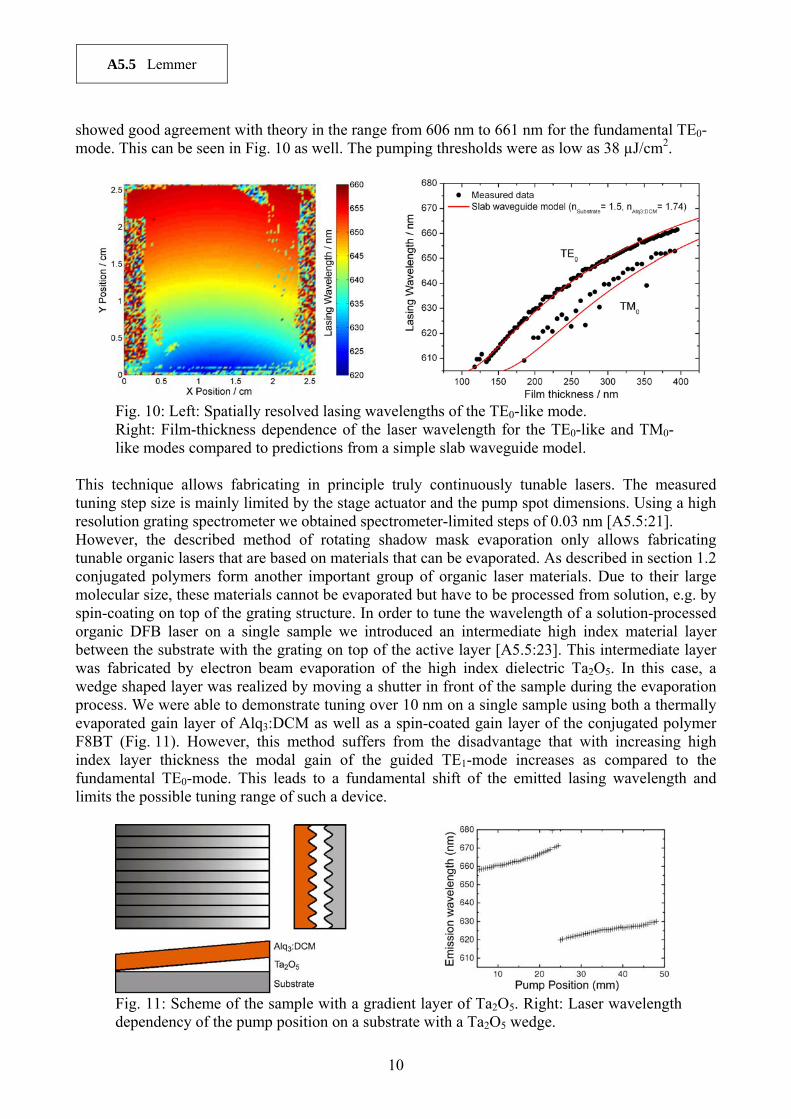
3. Tunable organic lasers Organic gain materials have the advantage of providing high energy conversion efficiencies over a broad spectral range. Thus, they are ideal candidates as active material for wavelength tunable laser devices. Applications for tunable lasers are widespread, e.g. in the field of spectroscopy, material diagnostics or sensing [57]. Therefore, we investigated different tuning principles for organic DFB lasers. From Equation 1 it can be seen that varying the grating pitch on one sample is the most simple way to modify the emission wavelength of a DFB laser. In Fig. 7, various lasing spectra of an organic DFB laser with varying grating period are shown. The pitch of the neighboring gratings varied in steps of 10 nm which results in discrete wavelengths steps of about 14 nm. As already described in section 2, corrugated substrates or masters of high quality are usually fabricated using electron beam lithography or interference lithography for structuring and subsequent developing and etching steps. Even though a continuous variation of the pitch is in principle possible using asymmetric interference exposure, a common way to vary the pitch is by sequentially exposing the resist which results in regions of varying pitch. Thus, the resolution of the used structuring method directly determines the grating period variation. For e.g. electron beam lithography, the resolution is on the order of 1 nm which also means that a possible laser wavelength variation is on the order of 1 nm as well. Thus, for tunable laser applications where a wavelength resolution below 1 nm is necessary, different tuning schemes for organic DFB lasers have to be developed. One method to tune the emission wavelength of an organic DFB laser is by varying the effective refractive index of the guided, resonant mode which can e.g. be achieved by a variation of the film thickness. This has been demonstrated for the thermally evaporated small molecule complex Alq3:DCM in a discrete fashion [10] as well as with a continuous film-thickness variation [A5.5:16, A5.5:26]. For the latter, a thickness gradient of the resulting thin film was obtained by installing a particularly designed shadow mask coaxially between the rotating sample holder and the evaporation sources. The shadow mask is shown in Fig. 9 along with a photograph of a sample after the rotating shadow mask evaporation.
Fig. 9: Left: Photograph of the shadow mask used in the evaporation process. Right: Photograph of a sample after the rotating shadow mask evaporation.
It was designed such that a linear decrease of the film thickness from the inner side to the outer side is achieved as the opening angle of the openings decreases radially. The substrate grating with a period of 400 nm was fabricated by interference lithography on a glass slide with an edge length 2.5 cm. For the evaporation, we aligned the grating substrates such that the resulting thickness gradient was parallel to the grating lines in order to provide uniform optical feedback in the region of interest. The samples were scanned spatially and spectrally by moving the pump spot relative to the evacuated sample chamber. This resulted in a map of each sample giving the DFB laser emission wavelength for each position on the sample, as shown in Fig. 10. A correlation of the lasing wavelength with the position dependant film thickness as obtained from a reference sample
A5.5 Lemmer
10
showed good agreement with theory in the range from 606 nm to 661 nm for the fundamental TE0-mode. This can be seen in Fig. 10 as well. The pumping thresholds were as low as 38 µJ/cm2.
Fig. 10: Left: Spatially resolved lasing wavelengths of the TE0-like mode. Right: Film-thickness dependence of the laser wavelength for the TE0-like and TM0-like modes compared to predictions from a simple slab waveguide model.
This technique allows fabricating in principle truly continuously tunable lasers. The measured tuning step size is mainly limited by the stage actuator and the pump spot dimensions. Using a high resolution grating spectrometer we obtained spectrometer-limited steps of 0.03 nm [A5.5:21]. However, the described method of rotating shadow mask evaporation only allows fabricating tunable organic lasers that are based on materials that can be evaporated. As described in section 1.2 conjugated polymers form another important group of organic laser materials. Due to their large molecular size, these materials cannot be evaporated but have to be processed from solution, e.g. by spin-coating on top of the grating structure. In order to tune the wavelength of a solution-processed organic DFB laser on a single sample we introduced an intermediate high index material layer between the substrate with the grating on top of the active layer [A5.5:23]. This intermediate layer was fabricated by electron beam evaporation of the high index dielectric Ta2O5. In this case, a wedge shaped layer was realized by moving a shutter in front of the sample during the evaporation process. We were able to demonstrate tuning over 10 nm on a single sample using both a thermally evaporated gain layer of Alq3:DCM as well as a spin-coated gain layer of the conjugated polymer F8BT (Fig. 11). However, this method suffers from the disadvantage that with increasing high index layer thickness the modal gain of the guided TE1-mode increases as compared to the fundamental TE0-mode. This leads to a fundamental shift of the emitted lasing wavelength and limits the possible tuning range of such a device.
Fig. 11: Scheme of the sample with a gradient layer of Ta2O5. Right: Laser wavelength dependency of the pump position on a substrate with a Ta2O5 wedge.

A5.5 Lemmer
11
We also demonstrated the general applicability of such tunable organic DFB lasers as probing source in spectroscopic [A5.5:21, A5.5:26] or laser induced fluorescence measurements [A5.5:26]. We showed that the achieved resolution is comparable to that obtained by a commercial photospectrometer using a compact setup consisting of only few optical components (Fig. 12).
Fig. 12: Schematic of the optical setup and the detection scheme. Right: Comparison of a notch filter transmission curve measured using the tunable organic semiconductor laser (red) and a Cary 5 photospectrometer (black).
We were able to detect resonance shifts of 0.5 nm of an immersed photonic crystal slab upon variation of the cladding refractive index and probing with the tunable organic laser. This shift is comparable to the one obtained in a similar biosensing experiment using two crossed polarisers and a green LED where a 2.5 nMol streptavidin solution was detected [A5.5:27]. This demonstrates the potential of tunable organic lasers for spectroscopic investigations of biological systems. Our current research activities are focusing on a scheme that allows tuning of organic DFB lasers by covering the slab waveguide with a layer of liquid crystals. These liquid crystals are aligned by an electrical field between laterally aligned electrodes which allows tuning the wavelength of such a laser by just changing the applied voltage. This method has the advantage that sample and excitation pump spot do not have to be moved with respect to each other. This approach is a promising way to tune the lasing wavelength of organic DFB lasers integrated in photonic circuits. A manuscript about this work is currently in preparation. 4. Integration of organic lasers into optical sensor systems A major advantage of organic laser materials is the fact that this material group and thus also devices made out of these can easily be integrated into micro-optical or photonic circuits. A scheme of the proposed integration of organic lasers as light sources in LOC systems is shown in Fig. 13. Light of the optically pumped organic lasers is coupled into a polymeric waveguide. The laser light is guided to the detection area at the cross-section of the waveguide and a microfluidic channel. The resulting optical signal, e. g., a change in the absorption pattern or a laser-induced fluorescent signal might then be detected by an integrated photodiode (which could also be an organic one). In conventional analysis systems often several solid state or gas lasers are needed to generate light at different wavelengths, rendering these systems complex and expensive. In our concept [58, 59, 60, A5.5:15, A5.5:25], several organic lasers with different emission wavelengths will be integrated on a single chip. The proposed portable LOC systems optical pumping avoids the need for electronic interconnects which potentially facilitates its use in point-of-care diagnostics.

A5.5 Lemmer
12
Fig. 13: Scheme of a possible LOC design incorporating a microfluidic system for analyte preparation and handling, multiple nanophotonic laser sources and photodetection by organic photodiodes.
Within the project, mainly the polymer Poly(methyl methacrylate) (PMMA) which is well suited for hot embossing nanostructures has been used as the substrate material. Additionally, PMMA is a low-cost biocompatible material [61]. It is also quite simple to define stripe waveguides in PMMA as it exhibits a significant change of the refractive index after exposure to UV light of a short wavelength (often referred to as deep UV, DUV) [62]. 4.1 Waveguide coupled organic semiconductor lasers The above mentioned fabrication techniques enabled the fabrication of an integrated waveguide coupled organic semiconductor laser. This work is done in close collaboration with the Institut für Microstrukturtechnik of the KIT. We have shown the coupling of amplified spontaneous emission (ASE) generated in an organic semiconductor layer into an underlying deep UV patterned waveguide [A5.5:8]. Recently, an integrated laser with strongly (20x) enhanced coupling efficiency has been demonstrated [A5.5:9]. The coupling efficiency could even be more improved by introducing a topographical step between the grating region of the DFB laser and the waveguide region [A5.5:18, A5.5:20]. The waveguide coupled lasers were fabricated with three main process steps.
Hot embossing of first order DFB laser resonators Waveguide definition through deep UV exposure of PMMA Deposition of the active laser material via thermal evaporation
Fig. 14: Schematic of the process chain for the fabrication of integrated waveguide coupled organic solid state lasers.
A5.5 Lemmer
13
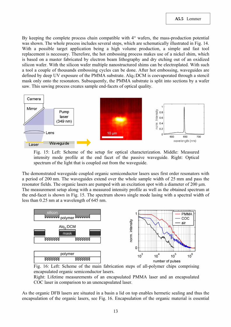
By keeping the complete process chain compatible with 4“ wafers, the mass-production potential was shown. The whole process includes several steps, which are schematically illustrated in Fig. 14. With a possible target application being a high volume production, a simple and fast tool replacement is necessary. Therefore, the hot embossing process makes use of a nickel shim, which is based on a master fabricated by electron beam lithography and dry etching out of an oxidized silicon wafer. With the silicon wafer multiple nanostructured shims can be electroplated. With such a tool a couple of thousands embossing cycles can be done. After hot embossing, waveguides are defined by deep UV exposure of the PMMA substrate. Alq3:DCM is coevaporated through a stencil mask only onto the resonators. Subsequently, the PMMA substrate is split into sections by a wafer saw. This sawing process creates sample end-facets of optical quality.
Fig. 15: Left: Scheme of the setup for optical characterization. Middle: Measured intensity mode profile at the end facet of the passive waveguide. Right: Optical spectrum of the light that is coupled out from the waveguide.
The demonstrated waveguide coupled organic semiconductor lasers uses first order resonators with a period of 200 nm. The waveguides extend over the whole sample width of 25 mm and pass the resonator fields. The organic lasers are pumped with an excitation spot with a diameter of 200 µm. The measurement setup along with a measured intensity profile as well as the obtained spectrum at the end-facet is shown in Fig. 15. The spectrum shows single mode lasing with a spectral width of less than 0.25 nm at a wavelength of 645 nm.
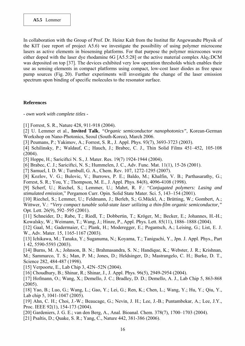
Fig. 16: Left: Scheme of the main fabrication steps of all-polymer chips comprising encapsulated organic semiconductor lasers. Right: Lifetime measurements of an encapsulated PMMA laser and an encapsulated COC laser in comparison to an unencapsulated laser.
As the organic DFB lasers are situated in a basin a lid on top enables hermetic sealing and thus the encapsulation of the organic lasers, see Fig. 16. Encapsulation of the organic material is essential

A5.5 Lemmer
14
for long time operation as the material degrades under optical pumping due to photooxidation. This simple, wafer-scale encapsulation technique was demonstrated to work for PMMA as well as cyclic olefin copolymer (COC) giving 11-fold and 3-fold improvement of the operation lifetime respectively [A5.5:29]. This work was conducted in collaboration with the group of Prof. Dr. Anders Kristensen at DTU Nanotech in Denmark. 4.2 Integrated fluorescence excitation using organic semiconductor lasers In a next step, we fabricated DFB lasers and a microfluidic channel in PMMA, connected with each other by a deep UV defined waveguide (Fig. 17) [63]. The microfluidic channel was filled with two different solutions: (1) carboxylate-modified microspheres (FluoSpheres®, dark red fluorescent, 660⁄680) of 0.04 µm in diameter mixed in aqueous solution to a concentration of 1% solids acquired from Sigma-Aldrich® and (2) goat anti-mouse IgG antibodies labelled with Alexa Fluor® 647 mixed in PBS buffer solution to a concentration of 2 mg/mL acquired from InvitrogenTM. Both, DFB laser and microfluidic channel were sealed with a lid. By pumping the DFB laser, its emitted light was coupled into the waveguide and guided to the crossing of waveguide and microfluidic channel where the DFB laser light excited the fluorophores. This was detected with a microscope objective and a spectrometer as shown in Fig. 18.
Fig. 17: Left: (a) Scheme of an all-organic laser-lab on a chip system as used for fluorescence excitation and (b) sectional view of one detection unit on the same system (not to scale). Right: Schematic illustration of the optical setup to prove the functional capability of fluorescence excitation on all-organic chips.
Fig. 18: (a) Input-output curve of an integrated laser and (b) laser and fluorescence spectrum taken at the interaction zone as shown in Fig. 3 without using a long pass filter to block the laser light.

A5.5 Lemmer
15
4.3 Biosensing schemes for photonic lab-on-chip systems In order to provide a LOC platform that allows the detection of a small number of molecules we also investigated a photonic bio-transducer that can easily be combined with deep UV defined waveguides. Using the technique of dip-pen nanolithography, a functional waveguide grating coupler out of the phospholipid 1,2-dioleoyl-sn-glycero-3-phosphocholine (DOPC) was patterned onto a waveguide [A5.5:22]. The different wavelengths of the white light that was externally coupled into that waveguide was coupled out by the grating at different angles as shown in Fig. 19.
Fig. 19: Left: Schematic of the waveguide grating couplers. Light of a supercontinuum laser source is coupled into a single-mode strip waveguide and decoupled by the grating coupler. Right: Photographs of the coupler at 30° and 45° from the surface normal, where the red and green portions of the guided supercontinuum light are coupled to radiation modes, respectively.
The DOPC structures were shown to undergo a change of size and shape upon protein binding which also affects the diffraction efficiency. By this, we were able to detect binding of an analyte to the functionalized DOPC gratings with concentrations as low as 5 nMol. Thus, such a grating coupler is one possible route as a transducer for an advanced detection scheme of biologically relevant molecules [A5.5:24]. This work was the result of a successful collaboration with Steven Lenhert and coworkers from the Institut für Nanotechnologie of the KIT. Another very sensitive biosensing element was introduced by Vahala et al. [64]. Microresonators are known to exhibit sharp resonances due to the whispering gallery modes propagating in such a geometry. These resonances are sensitive to changes of the cavity surrounding and thus enable single-molecule detection.
Fig. 20: Left: Schematic cross sectional view of the conical PMMA microcavity with a thin layer of Alq3:DCM on top. Right: Emission spectra of the microcavity laser at increasing pump energies using the laser diode as pump source.
A5.5 Lemmer
16
In collaboration with the Group of Prof. Dr. Heinz Kalt from the Institut für Angewandte Physik of the KIT (see report of project A5.6) we investigate the possibility of using polymer microcone lasers as active elements in biosensing platforms. For that purpose the polymer microcones were either doped with the laser dye rhodamine 6G [A5.5:28] or the active material complex Alq3:DCM was deposited on top [37]. The devices exhibited very low operation thresholds which enables their use as sensing elements in compact platforms using compact, low-cost laser diodes as free space pump sources (Fig. 20). Further experiments will investigate the change of the laser emission spectrum upon binding of specific molecules to the resonator surface. References - own work with complete titles - [1] Forrest, S. R., Nature 428, 911-918 (2004). [2] U. Lemmer et al., Invited Talk, “Organic semiconductor nanophotonics”, Korean-German Workshop on Nano-Photonics, Seoul (South-Korea), March 2006. [3] Peumans, P.; Yakimov, A.; Forrest, S. R., J. Appl. Phys. 93(7), 3693-3723 (2003). [4] Schilinsky, P.; Waldauf, C.; Hauch, J.; Brabec, C. J., Thin Solid Films 451–452, 105-108 (2004). [5] Hoppe, H.; Sariciftci N. S., J. Mater. Res. 19(7) 1924-1944 (2004). [6] Brabec, C. J.; Sariciftci, N. S.; Hummelen, J. C., Adv. Func. Mat. 11(1), 15-26 (2001). [7] Samuel, I. D. W.; Turnbull, G. A., Chem. Rev. 107, 1272-1295 (2007). [8] Kozlov, V. G.; Bulovic, V.; Burrows, P. E.; Baldo, M.; Khalfin, V. B.; Parthasarathy, G.; Forrest, S. R.; You, Y.; Thompson, M. E., J. Appl. Phys. 84(8), 4096-4108 (1998). [9] Scherf, U.; Riechel, S.; Lemmer, U.; Mahrt, R. F.: “Conjugated polymers: Lasing and stimulated emission,” Pergamon Curr. Opin. Solid State Mater. Sci. 5, 143–154 (2001). [10] Riechel, S.; Lemmer, U.; Feldmann, J.; Berleb, S.; G.Mückl, A.; Brütting, W.; Gombert, A.; Wittwer, V.: “Very compact tunable solid-state laser utilizing a thin-film organic semiconductor,” Opt. Lett. 26(9), 592–595 (2001). [11] Schneider, D.; Rabe, T.; Riedl, T.; Dobbertin, T.; Kröger, M.; Becker, E.; Johannes, H.-H.; Kowalsky, W.; Weimann, T.; Wang, J.; Hinze, P., Appl. Phys. Lett. 85(11), 1886–1888 (2004). [12] Gaal, M.; Gadermaier, C.; Plank, H.; Moderegger, E.; Pogantsch, A.; Leising, G.; List, E. J. W., Adv. Mater. 15, 1165-1167 (2003). [13] Ichikawa, M.; Tanaka, Y.; Suganuma, N.; Koyama, T.; Taniguchi, Y., Jpn. J. Appl. Phys., Part 1 42, 5590-5593 (2003). [14] Burns, M. A.; Johnson, B. N.; Brahmasandra, S. N.; Handique, K.; Webster, J. R.; Krishnan, M.; Sammarco, T. S.; Man, P. M.; Jones, D.; Heldsinger, D.; Mastrangelo, C. H.; Burke, D. T., Science 282, 484-487 (1998). [15] Verpoorte, E., Lab Chip 3, 42N–52N (2004). [16] Choudhury, B.; Shinar, R.; Shinar, J., J. Appl. Phys. 96(5), 2949-2954 (2004). [17] Hofmann, O.; Wang, X.; Demello, J. C.; Bradley, D. D.; Demello, A. J., Lab Chip 5, 863-868 (2005). [18] Yao, B.; Luo, G.; Wang, L.; Gao, Y.; Lei, G.; Ren, K.; Chen, L.; Wang, Y.; Hu, Y.; Qiu, Y., Lab chip 5, 1041-1047 (2005). [19] Ahn, C. H.; Choi, J.-W.; Beaucage, G.; Nevin, J. H.; Lee, J.-B.; Puntambekar, A.; Lee, J.Y., Proc. IEEE 92(1), 154-173 (2004). [20] Gardeniers, J. G. E.; van den Berg, A., Anal. Bioanal. Chem. 378(7), 1700–1703 (2004). [21] Psaltis, D.; Quake, S. R.; Yang, C., Nature 442, 381-386 (2006).

A5.5 Lemmer
17
[22] Balslev, S.; Jorgensen, A. M.; Bilenberg, B.; Mogensen, K. B.; Snakenborg, D.; Geschke, O.; Kutter, J. P.; Kristensen, A., Lab Chip 6, 213–217 (2006). [23] Punke, M.; Mozer, S.; Stroisch, M.; Bastian, G.; Gerken, M.; Lemmer, U.; Rabus, D.G.; Henzi, P.: “Organic semiconductor devices for micro-optical applications,” Proc. SPIE 6185, 618505-1-618505-13 (2006). [24] Christiansen, M. B.; Schøler, M.; Kristensen, A., Opt. Exp. 15, 3931-3939 (2007). [25] Schneider, D.; Lemmer, U.; Riedl, T.; Kowalsky, W.: “Low threshold organic semiconductor lasers,” Organic Light Emitting Devices, K. Müllen and U. Scherf, Editors. Wiley-VCH, Weinheim, (2005). [26] W. Kowalsky et al., Invited Talk, Organic semiconductor distributed feedback lasers, Optics East 2005, Boston, USA, October 2005. [27] Friend, R. H., Gymer, R. W., Holmes, A. B., Burroughes, J. H., Marks, R. N., Taliani, C., Bradley, D. D. C., Santos,D.A.D.,Brédas, J. L., Lögdlund, M., and Salaneck, W. R., Nature 397, 121–128 (1999). [28] Hide, F., Diaz-Garcia, M. A., Schwartz, B. J., Andersson, M. R., and Heeger, A. J., Science 273, 1833–1836 (1996). [29] Kozlov, V. G., Bulovic, V., Burrows, P. E., and Forrest, S. R., Nature 389, 362–364 (1997). [30] Schneider, D., Rabe, T., Riedl, T., Dobbertin, T., Kröger, M., Becker, E., Johannes, H.-H., Kowalsky, W., Weimann, T., Wang, J., and Hinze, P., Applied Physics Letters 85, 1659–1661 (2004). [31] Ribierre, J. C., Tsiminis, G., Richardson, S., Turnbull, G. A., Samuel, I. D. W., Barcena, H. S., and Burn, P. L., Applied Physics Letters 91(8), 081108 (2007). [32] Schneider, D., Technical University Braunschweig, Ph.D. thesis (2005). [33] Turnbull, G. A.; Andrew, P; Barnes, W. L,.; Samuel, I.D.W., Appl. Phys. Lett. 82, 313 (2003). [34] U. Lemmer et al., Invited Talk, Advances in organic semiconductor lasers, Frontiers in Optics Conferences during OSA annual meeting 2005, Tucson, USA, October 2005. [35] Karnutsch, C.; Haug, V.; Gärtner, C.; Lemmer, U.; Farrell, T.; Nehls, B.; Scherf, U.; Wang, J.; Weimann, T.; Heliotis, G.; Pflumm, C.; deMello, J.C.; Bradley, D.D.C.: “Low threshold blue conjugated polymer DFB lasers,” CLEO, CFJ3 (2006). [36] Yang, Y.; Turnbull, G. A.; Samuel, I. D. W., Appl. Phys. Lett. 92, 163306 (2008). [37] S. Klinkhammer, T. Großmann, K. Lüll, M. Hauser, C. Vannahme, T. Mappes H. Kalt, and U. Lemmer, “Diode-Pumped Organic Semiconductor Microcone Laser”, submitted (2010). [38] Campbell,V; Smith, D.; Neef, C.; Ferraris, J., Appl. Phys. Lett. 75(6), 841–843 (1999). [39] Yokoyama, W.; Sasabe, H.; Adachi, C., Jpn. J. Appl. Phys. 42, L1353–L1355 (2003). [40] Yamamoto, H.; Kasajima, H.; Yokoyama, W.; Sasabe, H.; Adachi, C., Appl. Phys. Lett. 86, 083502 (2005). [41] Gärtner, C.; Karnutsch, C.; Pflumm, C.; Lemmer, U.: “Numerical Device Simulation of Double Heterostructure Organic Laser Diodes Including Current Induced Absorption Processes,” IEEE J. Quantum Electron. 43(11), 1006-1017 (2007). [42] Kavc, T.; Langer, G.; Kern, W.; Kranzelbinder, G.; Toussaere, E.; Turnbull, G. A.; Samuel, I. D. W.; Iskra, K. F.; Neger, T.; Pogantsch, A., Chem. Mat. 14, 4178-4185 (2002). [43] Lawrence, J.R.; Andrew, P.; Barnes, W.L.; Buck, M; Turnbull, G. A.; Samuel, I. D. W., Appl. Phys. Lett. 81, 1955-1958 (2002). [44] Pisignano, D.; Persano, L.; Visconti, P; Cingolani, R.; Gigli, G., Appl. Phys. Lett. 83, 2545 (2003). [45] Forberich, K., “Organische Photonische-Kristall-Laser“, University of Freiburg, Ph.D. thesis (2005). [46] Gombert, A.; Bläsi, B.; Bühler, C.; Nitz, P.; Mick, J.; Hoßfeld, W.; Niggemann, M., Opt. Eng. 43, 2525-2533 (2004). [47] Srinivasan, R.; Braren, B., Chem. Rev., 89, 1303-1316 (1989).

A5.5 Lemmer
18
[48] Chou, S.Y.; Krauss, P.R.; Renstrom, P. J., Science 272(5258), 85 (1996). [49] Hanemann, T.; Heckele, M.; Piotter, V., Polymer News 25, 224-229 (2000). [50] Bacher, W.;Menz, W.; Mohr, J., Industrial Electronics, IEEE Transactions on 42(5), 431-441, (1995). [51] Mappes, T.; Worgull, M.; Heckele, M.; Mohr, J., Microsyst. Technol., DOI: 10.1007/s00542-007-0499-6, (2008). [52] Gale, M.T., Microelectron Engineering 34(3) (1997). [53] Kim, I.; Mentone, P.F., Electrochim. Acta 52 (2006). [54] Berggren, M.; Dodalapur, A.; Slusher, R.E., Appl. Phys. Lett. 72(4), 410–411 (1998). [55] Meier, M.; Dodabalapur, A.; Rogers, J. A.; Slusher, R. E.; Mekis, A.; Timko, A., J. Appl. Phys. 86(7), p. 3502–3507 (1999). [56] Eschenbaum, C., Woggon, T., Lemmer, U., “High Speed Fabrication of Toroidal Micro-Ring Resonators by Two Photon Direct Laser Writing”, Nonlinear Photonics (paper NThB8), OSA Technical Digest (CD), Optical Society of America (2010). [57] Duarte, F.J., (Ed.), Tunable Laser Applications, Second Edition (CRC, New York, 2009) [58] U. Lemmer et al, Invited Talk., Organic semiconductor lasers for integrated sensor systems, SPIE Symposium on Photonic Devices + Applications, San Diego, USA, August 2008. [59] U. Lemmer et al., Invited Talk, Organic semiconductor lasers as integrated light sources for optical sensor systems, Plastic Electronics 2007, Frankfurt, Germany, October 2007. [60] M. Punke et al., Invited Talk, Organic semiconductor devices for micro-optical applications, SPIE Symposium on Micro-Optics, VCSELs, and Photonic Interconnects: Fabrication, Packaging, and Integration, Strasbourg, France, May 2006. [61] Rabus, D.G.; Bruendel, M.; Ichihashi, Y.; Welle, A.; Seger, R.A.; Isaacson, M., IEEE J. Sel. Top. Quantum Electron. 13(2), 214–222 (2007). [62] Ruck, D.M.;.Brunner, S.; Tinschert, K.; Frank, W. F. X., Nucl. Instrum. Methods Phys. Res., Sect. B 106(1-4), 447-451 (1995). [63] Vannahme, C., Klinkhammer, S., Lemmer, U., Mappes, T., “Plastic lab-on-a-chip for fluorescence excitation with organic semiconductor lasers”, submitted (2010). [64] Armani, A. M., Kulkarni, R.P., Fraser, S.E., Flagan, R.C., Vahala, K.J., Science, vol. 317, pp. 783–787 (2007).