Organic flashmemory
23
Organic Flash Memory Gizem MERCAN 2009510051
-
Upload
gizem-mercan -
Category
Engineering
-
view
88 -
download
2
Transcript of Organic flashmemory

Organic Flash MemoryGizem MERCAN 2009510051


The demand on memory device elements based on organic materials grows rapidly
Since they require low-cost for manufacturing
Yield high perfomance in technological applications.
There are many organic materials that are being used as memory device elements that provide fast.
Information About Organic Memory Devices

Information About Organic Memory Devices
Non-volatile memory which should retain for at least 10 years.
It should provide high density data storage.
High writing/reading stability.
Long retention time.

What are principles of design?
A typical organic memory device is based on deposition of a low cost polymer film on an active organic material.
The organic memory devices are made using organic bistability materials employ ideal on/off ratio,
Moderate read/write voltage,
Quicker response time have potential applications in RAM,ROM and flash memory.

Types of Organic Memory Devices
Generation of memory in organic devices can be achieved by charge storage in terms of charge trapping, charge separation, and change transfer within the active components of the organic layer.
Thus the material used should provide an energy barrier to prevent recombination of negative and positive charges.
Then after the materials are polarized, conductance of the device changes, where the low conductance state is the OFF state and the high-conductance state is the ON state.

Types of Organic Memory Devices
This process where the electrically bistable materials are switched from low conductive state (0) to high conductive state (1) by the applied voltage is called writing.
When the process is reversed by applying a reverse bias voltage as from high conductive state to low conductive state, device performs erasing.
Roughly, Organic Memory Devices can be investigated under three categories :
1. Resistive switch and write once, read many times (WORM) devices,
2. Molecular Memory Devices.
3. Polymer Memory Devices (PMDs).

Resistive switch&Worm and Moleculer Memory Device
A resistive material which is an active thin film is sandwiched between these electrodes.
Highly ordered monolayer of molecules is placed between the electrodes.

Polymer Memory Device
An organic material layer consisting of mixture of molecules and nanoparticles in an organic polymer matrix is placed between the electrodes instead of a molecular monolayer.

Flash Memory
Flash memory is a non volatile computer storage chip that can be electrically erased and programmed.
It was developed eeprom and must be erased in fairly large blocks before these can be rewritten with new data.
The high density NAND type must also be programmed and read in (smaller) blocks, or pages, while the NOR type allows a single machine word (byte) to be written or read independently.
The NAND type is primarily used in memory cards, Usb drives, solid-state drives, and similar products, for general storage and transfer of data.

Principle of Operations
Flash memory stores information in an array of memory cells made from floating-gate transistors. In traditional single-level cell (SLC) devices, each cell stores only one bit of information. Some newer flash memory, known as multi-level cell (MLC) devices
NOR flash: Each cell has one end connected directly to ground, and the other end connected directly to a bit line.
Default state is logically equivalent to a binary "1" value. A NOR flash cell can be programmed, or set to a binary "0" value. NAND flash: NAND flash also uses floating-gate transistors, but
they are connected in a way that resembles a Nand-gate. NAND flash uses tunnel injection for writing and tunnel release for
erasing. NAND flash memory forms the core of the removable Usb storage devices known as Usb Flash Drives, as well as most memory card formats and ssd available today.

Floating-gate transistors
• In flash memory, each memory cell resembles a standard MOSFET, except the transistor has two gates instead of one. On top is the control gate (CG), as in other MOS transistors, but below this there is a floating gate (FG) insulated all around by an oxide layer. The FG is interposed between the CG and the MOSFET channel.

Organic Flash Memory
The University of Tokyo developed the ‘organic flash memory’ a non volatile memory(gecici olmayan bellek) that has the same basic structure as a flash memory and is made with organic materials.(group led by Takeo Someya and Tsuyoshi Sekitani)
The erasing and reading voltages of the new flash memory are as low as 6V and 1V,respectively.Data can be written in and erased from the memory more than 1000 times.

Organic Flash Memory With its flexibility,the
flash memory can be used for large area sensors.
electronic paper and other large-area electronic devices if its memory retention time can be extended.

Organic Flash Memory

Organic Flash Memory
The research group used a polyethylene naphthalate(PEN) resin sheet as a substrate and arranged 26x26 2T memory cells in an array structure on it.
The sheet is flexible.the university comfirmed that it can be bent until its curvature radius 6mm without causing mechanical or electrical degradation.
Also comfirmed that the sheet can be used as a non volatile memory.
The memory array.The white parts are control gates and watery blue parts under three electrodes are pentacene(is a polycyclic aromatic hydrocarbon consisting of
five linearly-fused benzene rings.)
Organic Flash Memory
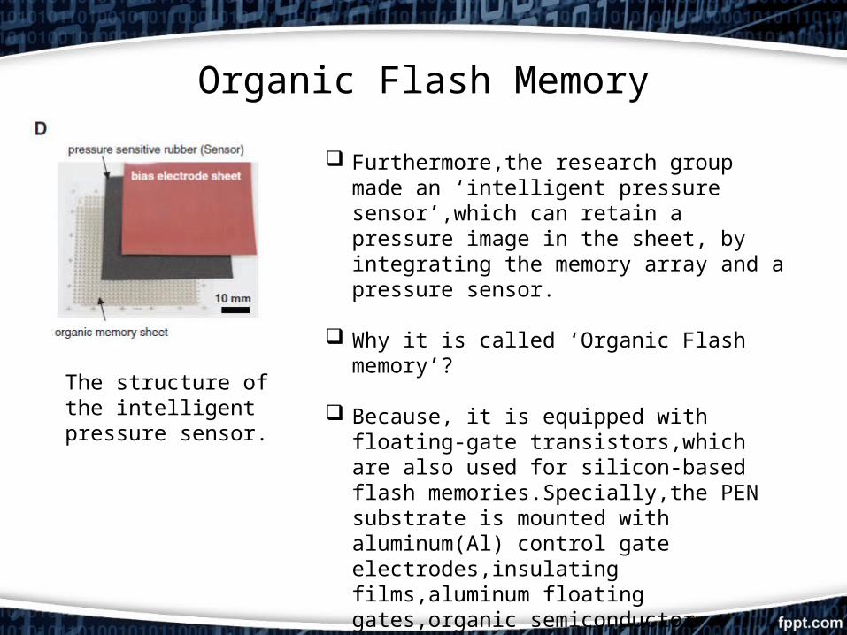
The structure of the intelligent pressure sensor.
Furthermore,the research group made an ‘intelligent pressure sensor’,which can retain a pressure image in the sheet, by integrating the memory array and a pressure sensor.
Why it is called ‘Organic Flash memory’?
Because, it is equipped with floating-gate transistors,which are also used for silicon-based flash memories.Specially,the PEN substrate is mounted with aluminum(Al) control gate electrodes,insulating films,aluminum floating gates,organic semiconductor pentacene and source and gate electrodes made of gold(Au).

Organic Flash Memory
The insulating film was made by using a self-assembled monolayer(SAM),which is made of kind of phosphoric acid having an alkyl chain(CH2-CH2…)in addition AlOx.
The SAM is as thin as 2nm.

Advantages of Organic Flash Memory
There are non volatile memories developed past.One is made by using ferroelectric materials, and the other has a floating-gate structure like the latest non volatile memory.
However,It is difficult to lower the writing and erasing voltages of the previous memory than 20V.
Also it becomes unstable when exposed to air because its memory properties fluctuate due to the nonconstant thickness of the insulating film.
At this time, SAM whose insulating film does not require thickness checking to reduce the variation in memory properties.
Moreover, the SAM is stable in atmosphere.

Disadvantages
The new organic flash memory has a memory retention time of only one day.
But this can be improved by reducing the size of element and employing an SAM with a long molecular length.

References• Chen Qi , Bai Hua, Shi GaoQuan, Memory devices based on organic electric bistable materials, Chinese Science
Bulletin, 200, 52(15), 2017-2023• J C. Scott, Is there an immortal memory?, Science, 2004, 304(5667), 62-63• DOI: 10.1126/science.1179963• Science 326, 1516 (2009);• Tsuyoshi Sekitani, et al.• Sensor Arrays• Organic Nonvolatile Memory Transistors for Flexible• www.sciencemag.org (this information is current as of December 10, 2009 ):• The following resources related to this article are available online at• http://www.sciencemag.org/cgi/content/full/326/5959/1516• version of this article at:• Updated information and services, including high-resolution figures, can be found in the online• http://www.sciencemag.org/cgi/content/full/326/5959/1516/DC1• Supporting Online Material can be found at:• http://www.sciencemag.org/cgi/content/full/326/5959/1516#otherarticles• This article cites 22 articles, 2 of which can be accessed for free:• http://www.sciencemag.org/cgi/collection/app_physics• Physics, Applied• This article appears in the following subject collections:• http://www.sciencemag.org/about/permissions.dtl


Any Question?