Organic field effect transistorsw3.ualg.pt/~hgomes/chapter_OFETs.pdf2! Organic field effect...
62
Book Title First Author & Second Author Copyright © 2009 by Pan Stanford Publishing Pte Ltd www.panstanford.com Chapter Five Organic field effect transistors Henrique Leonel Gomes University of the Algarve, Department of Electronics and Informatics, Campus de Gambelas, 8005-139 Faro, Portugal [email protected] This chapter aims to provide the reader with a practical knowledge about electrical methods to measure organic thin film transistor devices. It presents a series of recipes, which allow the experimentalist to gain insight into the performance and limitations of the devices and circuits being measured. It also gives guidelines on how to correctly interpret the measurements and to provide feedback to the manufacturing process. Organic based transistors are particularly suited for sensing and biomedical applications. The operation of these devices is presented with particular emphasis on the electrical techniques to address them when operating in complex liquid environments. 1.1 INTRODUCTION In this chapter various aspects of the characterization and performance of organic thin film transistors (OTFT) are considered. The chapter begins by addressing first individual transistors and afterwards addresses the characterization of simple circuits such as logic gates and ring oscillators. At the transistor level, the emphasis is on how to (i) perform basic parameter extraction and quantify individual transistor
Transcript of Organic field effect transistorsw3.ualg.pt/~hgomes/chapter_OFETs.pdf2! Organic field effect...
Book Title First Author & Second Author Copyright © 2009 by Pan Stanford Publishing Pte Ltd www.panstanford.com
Chapter Five
Organic field effect transistors
Henrique Leonel Gomes University of the Algarve, Department of Electronics and Informatics, Campus de Gambelas, 8005-139 Faro, Portugal [email protected]
This chapter aims to provide the reader with a practical knowledge about electrical methods to measure organic thin film transistor devices. It presents a series of recipes, which allow the experimentalist to gain insight into the performance and limitations of the devices and circuits being measured. It also gives guidelines on how to correctly interpret the measurements and to provide feedback to the manufacturing process. Organic based transistors are particularly suited for sensing and biomedical applications. The operation of these devices is presented with particular emphasis on the electrical techniques to address them when operating in complex liquid environments.
1.1 INTRODUCTION
In this chapter various aspects of the characterization and performance of organic thin film transistors (OTFT) are considered. The chapter begins by addressing first individual transistors and afterwards addresses the characterization of simple circuits such as logic gates and ring oscillators. At the transistor level, the emphasis is on how to (i) perform basic parameter extraction and quantify individual transistor
2 ⎢ Organic field effect transistors
performance, (ii) gain insight on the ability of the device to operate over long periods of time by measuring its operational stability, (iii) identify reliability issues which cause device failure and (iv) identify and circumvent sources of variability in transistor parameters. At the circuit level, the focus is on how the non-ideal behaviour of individual transistors degrades circuit operation.
This chapter is organized in the following way. A brief history of the TFT is presented on section 2 together with the description of the typical the TFT architectures and the basic operation mechanism. The differences between a silicon based metal-oxide-semiconductor field effect transistor (MOSFET) and an organic TFT device are discussed in section 3. The ideal TFT electrical characteristics are derived. Due to the presence of impurities TFTs show some non-ideal characteristics. These are discussed in section 4. Emphasis is given to the physical meaning of the extracted parameters. Recipes to identify non-ideal effects caused by extrinsic factors such as, impurities, parasitic and imperfect metal contacts are also presented and discussed. The operational stability deserves special attention. Different types of instabilities are briefly explained. It is shown how to quantify and benchmark operational stability. Section 4 also addresses variability characterization and draws the attention for the importance of design layout that minimizes variability. Electronic active impurities or traps determine the transistor performance and stability. Section 5 outlines the effects of traps on the electrical properties and describes techniques to study traps using the transistor as a tool. These include the temperature dependence of the field effect mobility, thermal de-trapping experiments and small signal-impedance spectroscopy. Simple but important circuits types such as the inverter and the ring oscillator are presented in section 6. OTFT applications in bioelectronics are discussed in section 7. The major conclusions of this chapter are outline in section 8. This chapter ends with a list of questions to help the reader to apply the concepts learned to some practical examples.
1.2 Field effect Transistors ⎢ 3
1.2 FIELD EFFECT TRANSISTORS
A thin film transistor (TFT) is a device that uses an electric field to modulate the conduction of a channel located at the interface between a dielectric and semiconductor. Therefore, it is field effect transistor (FET) similar to the well-known metal oxide field effect transistor (MOSFET), which is the basic building block of modern integrated circuits. The development histories of TFTs and MOSFETs are parallel in time. The TFT concept was patented in 1925 by Julius edger Lilienfeld and in 1934 by Osker Heil but at the time no practical applications has emerged. In the 1960s several device structures and semiconductor materials like Te, CdSe, Ge and InSb were explored to fabricate TFTs. However, the competition from the MOSFET based on silicon technology forced the TFT to enter in a long period of hibernation. In the early 1970s the need for large area applications in flat panel displays motivates the search for alternatives to the crystalline silicon and the TFT found its niche of application. In 1979, the hydrated amorphous silicon (a-Si: H) becomes a forerunner as a semiconductor to fabricate TFTs. Since the mid-1980s, the silicon-based TFTs have successfully dominate the large area liquid crystal displays (LCD) technology and become the most important devices for active matrix liquid crystal and organic light emitting diode applications. In the meantime, TFTs based on organic semiconductor channel layers are introduced in the 1990s with electron mobility equivalent to that of a-Si: H. Nowadays, organic based thin film transistors (OTFTs) are the candidate for incorporation onto flexible substrates. A representative and particularly important example is full-color, video, flexible OLED displays. Small OLED displays on conventional glass substrates for mobile phone and PDA applications are rapidly growing and are displacing LCD screens in the small display sector. OFET technology could be an ideal back-plane for this application because of the close materials compatibility between OLEDs and OFETs and their excellent mechanical properties. The application niche for OFETs is not entirely defined. Smart cards, disposable electronics, and electronic skins are also currently under intense research.
4 ⎢ Organic field effect transistors
1.2.1 Basic operation of a TFT
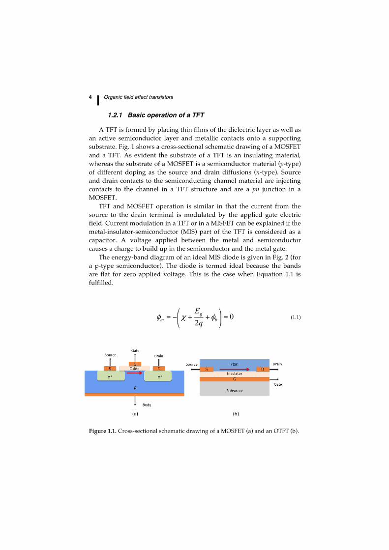
A TFT is formed by placing thin films of the dielectric layer as well as an active semiconductor layer and metallic contacts onto a supporting substrate. Fig. 1 shows a cross-sectional schematic drawing of a MOSFET and a TFT. As evident the substrate of a TFT is an insulating material, whereas the substrate of a MOSFET is a semiconductor material (p-type) of different doping as the source and drain diffusions (n-type). Source and drain contacts to the semiconducting channel material are injecting contacts to the channel in a TFT structure and are a pn junction in a MOSFET.
TFT and MOSFET operation is similar in that the current from the source to the drain terminal is modulated by the applied gate electric field. Current modulation in a TFT or in a MISFET can be explained if the metal-insulator-semiconductor (MIS) part of the TFT is considered as a capacitor. A voltage applied between the metal and semiconductor causes a charge to build up in the semiconductor and the metal gate.
The energy-band diagram of an ideal MIS diode is given in Fig. 2 (for a p-type semiconductor). The diode is termed ideal because the bands are flat for zero applied voltage. This is the case when Equation 1.1 is fulfilled.
02
=⎟⎟⎠
⎞⎜⎜⎝
⎛++−= b
gm q
Eφχφ (1.1)
Figure 1.1. Cross-sectional schematic drawing of a MOSFET (a) and an OTFT (b).

1.2 Field effect Transistors ⎢ 5
Figure 1.2. Band diagram of an ideal metal-insulator-semiconductor structure at equilibrium. ϕm is the metal work-function, qχ is the electron affinity measured from the bottom of the conduction band EC to the vacuum level, Eg the semiconductor bandgap, EV the semiconductor valence band, q the absolute electron charge, and Ef the Fermi level and Ei the intrinsic Fermi level.
Here, ϕm is the metal work-function, qχ is the electron affinity measured from the bottom of the conduction band EC to the vacuum level, Eg the semiconductor bandgap, q the absolute electron charge, and ϕb the potential difference between the Fermi level and the intrinsic Fermi level Ei (which is located very close to midgap) (in the non-ideal case, a small band curvature exists at the insulator-semiconductor interface, and a small potential Vfb, the so-called flat-band voltage, must be applied to the metal to get the flat-band conditions.)
When the MIS diode is biased with positive or negative voltages, three different situations may occur at the insulator-semiconductor interface. For a negative voltage (Fig. 1.3a), the bands bend upward and the top of the valence band moves closer to the Fermi level, causing an accumulation of holes near the insulator-semiconductor interface. The interface is thus more conductive than the bulk of the semiconductor. When a small to moderate positive voltage is applied to the gate electrode, majority carrier holes are repelled from the insulator/semiconductor interface so that a depletion layer is formed (Fig. 1.3b). When a larger positive voltage is applied to the metal (Fig. 1.3c), the bands bend even more downward and the intrinsic level eventually crosses the Fermi level. At this point, the density of electrons
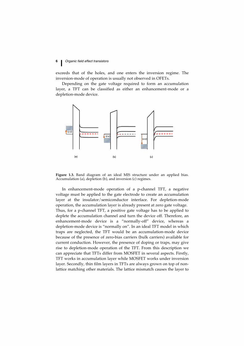
6 ⎢ Organic field effect transistors
exceeds that of the holes, and one enters the inversion regime. The inversion-mode of operation is usually not observed in OFETs.
Depending on the gate voltage required to form an accumulation layer, a TFT can be classified as either an enhancement-mode or a depletion-mode device.
Figure 1.3. Band diagram of an ideal MIS structure under an applied bias. Accumulation (a), depletion (b), and inversion (c) regimes.
In enhancement-mode operation of a p-channel TFT, a negative voltage must be applied to the gate electrode to create an accumulation layer at the insulator/semiconductor interface. For depletion-mode operation, the accumulation layer is already present at zero gate voltage. Thus, for a p-channel TFT, a positive gate voltage has to be applied to deplete the accumulation channel and turn the device off. Therefore, an enhancement-mode device is a “normally-off” device, whereas a depletion-mode device is “normally on”. In an ideal TFT model in which traps are neglected, the TFT would be an accumulation-mode device because of the presence of zero-bias carriers (bulk carriers) available for current conduction. However, the presence of doping or traps, may give rise to depletion-mode operation of the TFT. From this description we can appreciate that TFTs differ from MOSFET in several aspects. Firstly, TFT works in accumulation layer while MOSFET works under inversion layer. Secondly, thin film layers in TFTs are always grown on top of non-lattice matching other materials. The lattice mismatch causes the layer to
1.2 Field effect Transistors ⎢ 7
be amorphous with a high density of defects in particular at the dielectric/semiconductor interface. Thirdly, TFT is undoped while MOSFET is mostly Si-doped.
1.2.2 OTFT architectures
OTFTs can be fabricated on various types of rigid or flexible substrates, i.e., there is no need for an (expensive) single crystal wafer. There is no limit to the size or material properties of the substrate as long as it can stand the fabrication process environment. In addition, TFTs can be made from a wide range of semiconductor and dielectric materials.
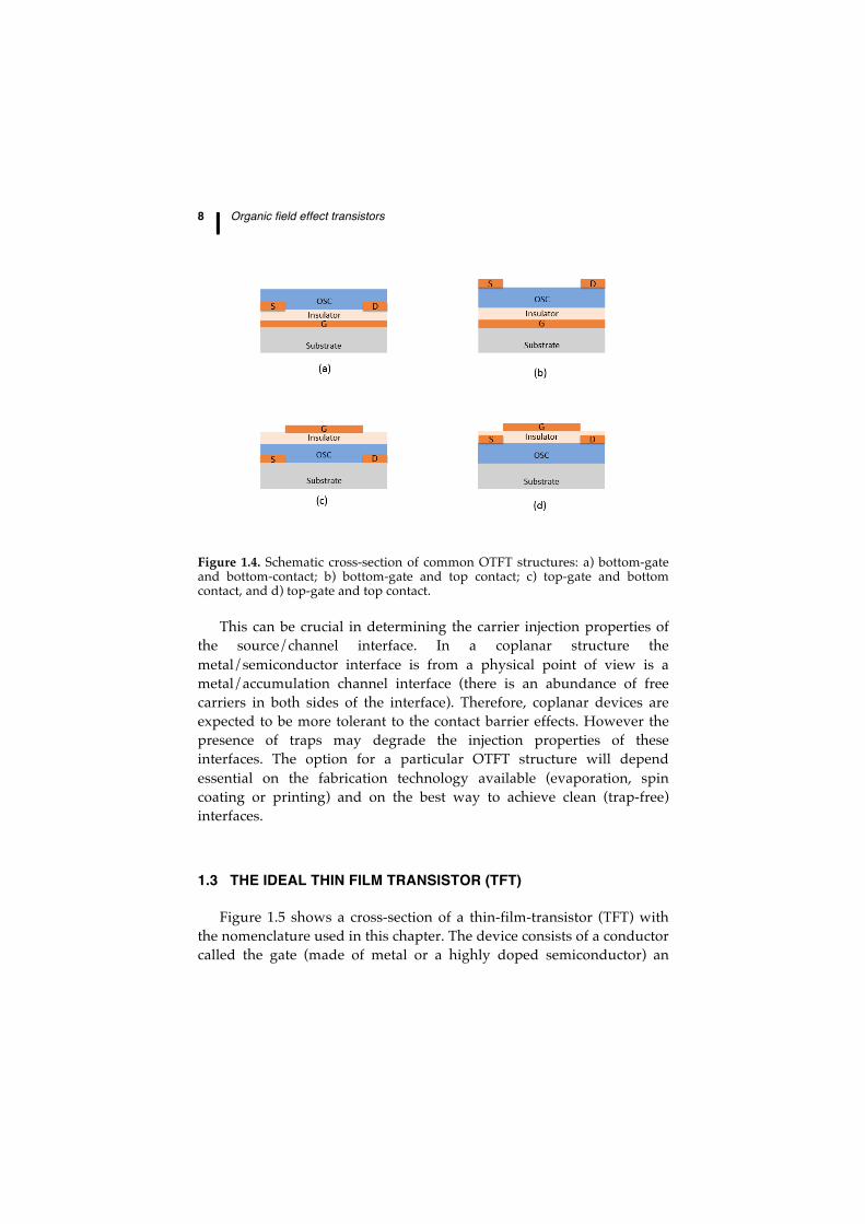
OTFT can be configured into four basic structures on the basis of position of the electrodes as shown in Fig. 1.4. The patterned source/drain electrodes can be deposited prior to the organic semiconductor (OSC) deposition or after it. The former case is a ‘‘coplanar’’ configuration (popularly called bottom contact) and the latter is ‘‘staggered’’ configuration (also known as top contact). Both the staggered and coplanar configurations are further categorized as bottom gate and top-gate structures. Different TFT structures can display quite dissimilar device characteristics while using the exact same materials. In a coplanar configuration, the source drain contacts and the insulator layer are on the same part of the channel whereas, in a staggered configuration, the source drain contacts and the insulator layer are on the opposite part of the channel.
8 ⎢ Organic field effect transistors
Figure 1.4. Schematic cross-section of common OTFT structures: a) bottom-gate and bottom-contact; b) bottom-gate and top contact; c) top-gate and bottom contact, and d) top-gate and top contact.
This can be crucial in determining the carrier injection properties of the source/channel interface. In a coplanar structure the metal/semiconductor interface is from a physical point of view is a metal/accumulation channel interface (there is an abundance of free carriers in both sides of the interface). Therefore, coplanar devices are expected to be more tolerant to the contact barrier effects. However the presence of traps may degrade the injection properties of these interfaces. The option for a particular OTFT structure will depend essential on the fabrication technology available (evaporation, spin coating or printing) and on the best way to achieve clean (trap-free) interfaces.
1.3 THE IDEAL THIN FILM TRANSISTOR (TFT)
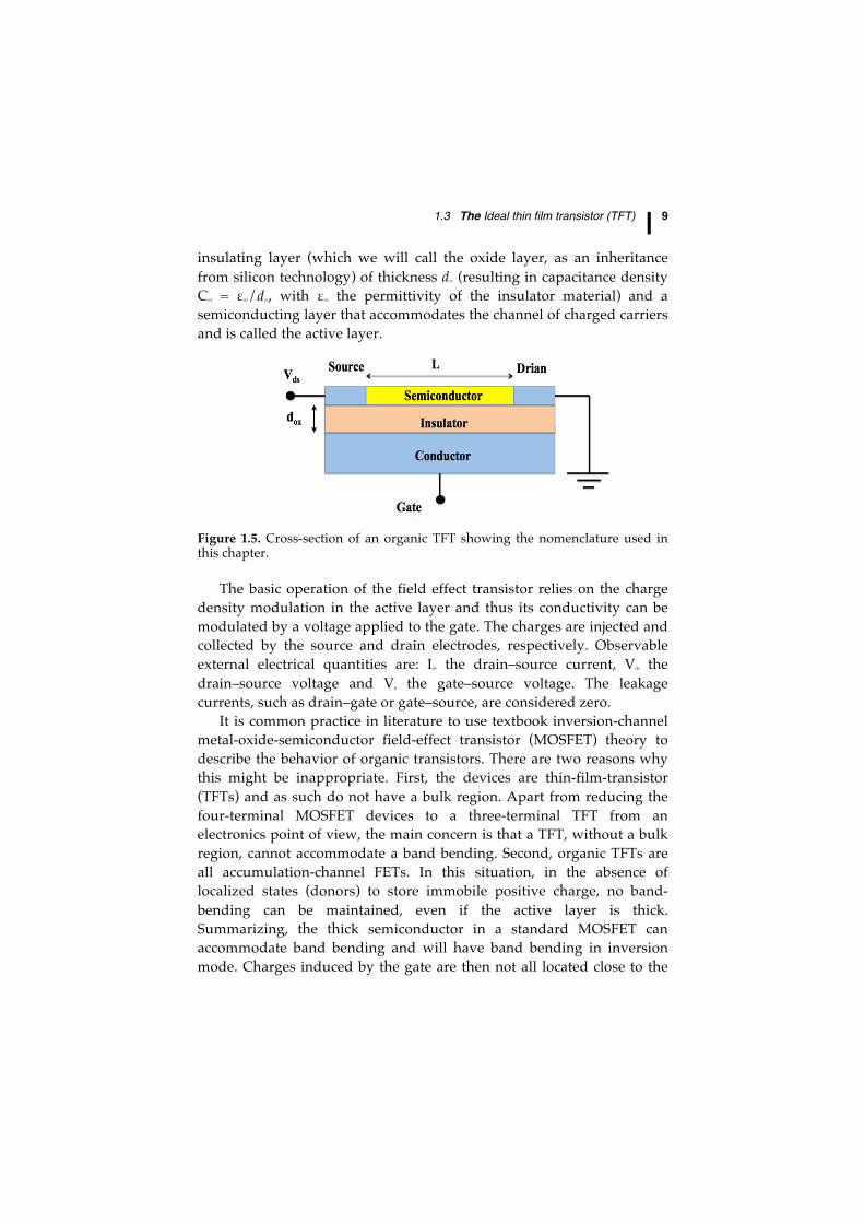
Figure 1.5 shows a cross-section of a thin-film-transistor (TFT) with the nomenclature used in this chapter. The device consists of a conductor called the gate (made of metal or a highly doped semiconductor) an
1.3 The Ideal thin film transistor (TFT) ⎢ 9
insulating layer (which we will call the oxide layer, as an inheritance from silicon technology) of thickness dox (resulting in capacitance density Cox = εox/dox, with εox the permittivity of the insulator material) and a semiconducting layer that accommodates the channel of charged carriers and is called the active layer.
Figure 1.5. Cross-section of an organic TFT showing the nomenclature used in this chapter.
The basic operation of the field effect transistor relies on the charge density modulation in the active layer and thus its conductivity can be modulated by a voltage applied to the gate. The charges are injected and collected by the source and drain electrodes, respectively. Observable external electrical quantities are: Ids the drain–source current, Vds the drain–source voltage and Vg the gate–source voltage. The leakage currents, such as drain–gate or gate–source, are considered zero.
It is common practice in literature to use textbook inversion-channel metal-oxide-semiconductor field-effect transistor (MOSFET) theory to describe the behavior of organic transistors. There are two reasons why this might be inappropriate. First, the devices are thin-film-transistor (TFTs) and as such do not have a bulk region. Apart from reducing the four-terminal MOSFET devices to a three-terminal TFT from an electronics point of view, the main concern is that a TFT, without a bulk region, cannot accommodate a band bending. Second, organic TFTs are all accumulation-channel FETs. In this situation, in the absence of localized states (donors) to store immobile positive charge, no band-bending can be maintained, even if the active layer is thick. Summarizing, the thick semiconductor in a standard MOSFET can accommodate band bending and will have band bending in inversion mode. Charges induced by the gate are then not all located close to the
10 ⎢ Organic field effect transistors
interface which leads to a complicated charge-voltage which reflects in the current-voltage relation results. In a thin-film-transistor, or in general an accumulation-type FET, all induced charge is necessarily close to the insulator and the charge–voltage relation is always simply:
( ) ( ) oxgCV-xV=xρ (1.2)
with ρ and V the local charge per area and voltage in the channel, respectively. This charge in a TFT might still be either mobile or immobile, though.
To give an idea of how thin the active layer in a TFT can be and still work properly: for a silicon based device, with −1 V at the gate relative to drain and source and an oxide thickness of dox = 200 nm, the induced charge is 0.17 mC/m2. With a density of states of NV of 1.04 × 1019 cm−3 and assuming continuity, this can fit into 1 Å which is less than the height of a monolayer. The TFTs have thus effectively two-dimensional charge distributions. This explains why, as has been shown, for organic FETs only the quality of the first monolayer matters. At best, the consecutive layers help to stabilize the integrity of the first layer, in terms of diffusion of impurities and crystallinity.
For standard MOSFETs, the assumption is made that the induced free charge in the channel is linearly depending on the gate bias. This is because, once the channel has been formed, all the charge induced by the gate is free charge. This in turn is caused by the type of semiconductor used in TFTs. For traditional materials, such as, Si or GaAs, the acceptors and donors introduce shallow levels, which are consequently all ionized at all operational temperatures. In organic semiconductors, the acceptor and donor states are very deep and abundant. As a result, even at room temperature, not all levels are ionized and temperature and bias can change the degree of occupancy. As we will show, the as-measured mobility does not change because of an increased depth of the acceptor level.
It is easy to show that the equation for currents of a MOSFET is also applicable to TFTs. In the case of a TFT the thickness of the channel is constant, but the density of charges p inside the channel varies from one electrode (“source”, x = 0) to the other (“drain”, x = L). To calculate the currents through the device, we have to understand that, locally, the current Ix(x) at a given point x in the channel is equal to the local
1.3 The Ideal thin film transistor (TFT) ⎢ 11
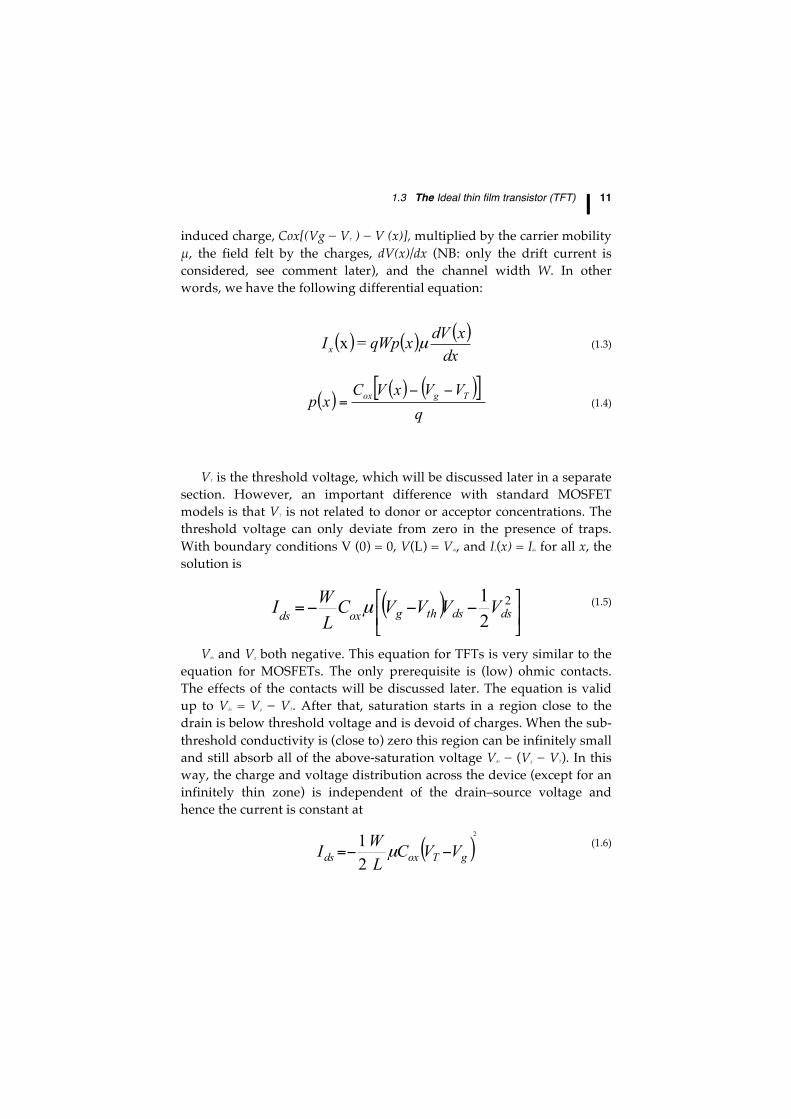
induced charge, Cox[(Vg − VT ) − V (x)], multiplied by the carrier mobility μ, the field felt by the charges, dV(x)/dx (NB: only the drift current is considered, see comment later), and the channel width W. In other words, we have the following differential equation:
( ) ( ) ( )dxxdVxqWpIx µ=x (1.3)
( ) ( ) ( )[ ]q
VVxVCxp Tgox −−= (1.4)
VT is the threshold voltage, which will be discussed later in a separate section. However, an important difference with standard MOSFET models is that VT is not related to donor or acceptor concentrations. The threshold voltage can only deviate from zero in the presence of traps. With boundary conditions V (0) = 0, V(L) = Vds, and Ix(x) = Ids for all x, the solution is
( ) ⎥⎦
⎤⎢⎣
⎡ −−−= 2
21
dsdsthgoxds VVVVCLWI µ (1.5)
Vds and Vg both negative. This equation for TFTs is very similar to the equation for MOSFETs. The only prerequisite is (low) ohmic contacts. The effects of the contacts will be discussed later. The equation is valid up to Vds = Vg − VT. After that, saturation starts in a region close to the drain is below threshold voltage and is devoid of charges. When the sub-threshold conductivity is (close to) zero this region can be infinitely small and still absorb all of the above-saturation voltage Vds − (Vg − VT). In this way, the charge and voltage distribution across the device (except for an infinitely thin zone) is independent of the drain–source voltage and hence the current is constant at
( )gToxds VVCLWI −−= µ21 2
(1.6)
12 ⎢ Organic field effect transistors
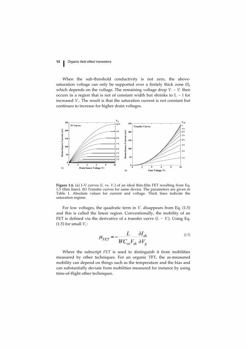
When the sub-threshold conductivity is not zero, the above-saturation voltage can only be supported over a finitely thick zone (l), which depends on the voltage. The remaining voltage drop VT − Vg then occurs in a region that is not of constant width but shrinks to L − l for increased Vds. The result is that the saturation current is not constant but continues to increase for higher drain voltages.
Figure 1.6. (a) I–V curves (Ids vs. Vds) of an ideal thin-film FET resulting from Eq. 1.5 (thin lines). (b) Transfer curves for same device. The parameters are given in Table 1. Absolute values for current and voltage. Thick lines indicate the saturation regime.
For low voltages, the quadratic term in Vds disappears from Eq. (1.5) and this is called the linear region. Conventionally, the mobility of an FET is defined via the derivative of a transfer curve (Ids − Vg). Using Eq. (1.5) for small Vds:
g
ds
dsoxFET V
IVWCL
∂∂−=µ (1.7)
Where the subscript FET is used to distinguish it from mobilities measured by other techniques. For an organic TFT, the as-measured mobility can depend on things such as the temperature and the bias and can substantially deviate from mobilities measured for instance by using time-of-flight other techniques.
1.3 The Ideal thin film transistor (TFT) ⎢ 13
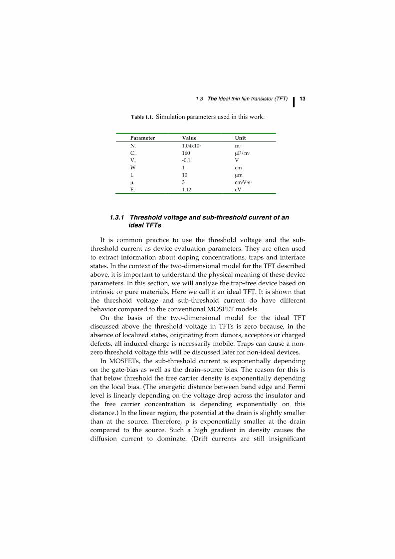
Table 1.1. Simulation parameters used in this work.
Parameter Value Unit NV 1.04x10¹⁶ m-2 COX 160 µF/m-2 Vds -0.1 V W 1 cm L 10 µm µo 3 cm2V-1s-1 Eg 1.12 eV
1.3.1 Threshold voltage and sub-threshold current of an ideal TFTs
It is common practice to use the threshold voltage and the sub-threshold current as device-evaluation parameters. They are often used to extract information about doping concentrations, traps and interface states. In the context of the two-dimensional model for the TFT described above, it is important to understand the physical meaning of these device parameters. In this section, we will analyze the trap-free device based on intrinsic or pure materials. Here we call it an ideal TFT. It is shown that the threshold voltage and sub-threshold current do have different behavior compared to the conventional MOSFET models.
On the basis of the two-dimensional model for the ideal TFT discussed above the threshold voltage in TFTs is zero because, in the absence of localized states, originating from donors, acceptors or charged defects, all induced charge is necessarily mobile. Traps can cause a non-zero threshold voltage this will be discussed later for non-ideal devices.
In MOSFETs, the sub-threshold current is exponentially depending on the gate-bias as well as the drain–source bias. The reason for this is that below threshold the free carrier density is exponentially depending on the local bias. (The energetic distance between band edge and Fermi level is linearly depending on the voltage drop across the insulator and the free carrier concentration is depending exponentially on this distance.) In the linear region, the potential at the drain is slightly smaller than at the source. Therefore, p is exponentially smaller at the drain compared to the source. Such a high gradient in density causes the diffusion current to dominate. (Drift currents are still insignificant
14 ⎢ Organic field effect transistors
because the densities are still too small.) The gradient and the current thus depend exponentially on Vds and Vg. The current is proportional to the difference in density at the source and the drain, Ids ∝ exp(Vg)−exp(Vg−Vds) ≈ exp(Vds)exp(Vg), which leads to the equation normally found in textbooks. Above threshold, the densities depend linearly on the potential and drift currents exceed the diffusion currents.
Because thin films do not have space to accommodate band bending, resulting in the basic Eq. (1.1), the charge density does not depend exponentially on the potential as in MOSFETs, but always linearly.
In summary, the similarity of the basic equation, Eq. (1.5) and Eq. (1.6), and the shapes of the curves of Fig. 1.6, with those obtained for inversion-channel MOSFETs, explain the persistence in literature of using the MOSFET model to describe organic TFTs; empirically, the curves are the same. The complications start when the measured data are analyzed and parameter extraction is attempted. The differences between MOSFETs and organic TFTs parameters are the following:
The threshold voltage in an ideal accumulation type organic TFT is zero. This is because, in the absence of localized states, originating from donors, acceptors or traps, all induced charge is necessarily mobile. Real organic TFTs are often non-ideal and they have a threshold voltage, however it is important to keep in mind that the threshold voltage is not an intrinsic device parameter in an organic TFT.
1.4 NON-IDEAL CHARACTERISTICS
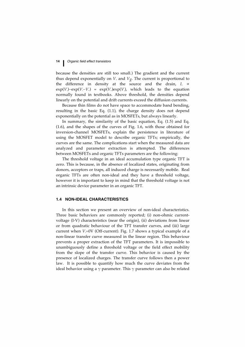
In this section we present an overview of non-ideal characteristics. Three basic behaviors are commonly reported; (i) non-ohmic current-voltage (I-V) characteristics (near the origin), (ii) deviations from linear or from quadratic behaviour of the TFT transfer curves, and (iii) large current when Vg=0V (Off-current). Fig. 1.7 shows a typical example of a non-linear transfer curve measured in the linear region. This behaviour prevents a proper extraction of the TFT parameters. It is impossible to unambiguously define a threshold voltage or the field effect mobility from the slope of the transfer curve. This behavior is caused by the presence of localized charges. The transfer curve follows then a power law. It is possible to quantify how much the curve deviates from the ideal behavior using a γ parameter. This γ parameter can also be related
1.4 Non-ideal characteristics ⎢ 15
with the density of localized states and its extraction will be discussed later.
Figure 1.7. Experimental transfer curve for an organic TFT based showing non-linear voltage dependence.
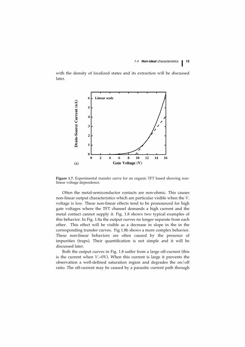
Often the metal-semiconductor contacts are non-ohmic. This causes non-linear output characteristics which are particular visible when the Vds voltage is low. These non-linear effects tend to be pronounced for high gate voltages where the TFT channel demands a high current and the metal contact cannot supply it. Fig. 1.8 shows two typical examples of this behavior. In Fig. 1.8a the output curves no longer separate from each other. This effect will be visible as a decrease in slope in the in the corresponding transfer curves. Fig 1.8b shows a more complex behavior. These non-linear behaviors are often caused by the presence of impurities (traps). Their quantification is not simple and it will be discussed later.
Both the output curves in Fig. 1.8 suffer from a large off-current (this is the current when Vgs=0V). When this current is large it prevents the observation a well-defined saturation region and degrades the on/off ratio. The off-current may be caused by a parasitic current path through
16 ⎢ Organic field effect transistors
the bulk region or by a built-in channel. The application of a positive gate bias should help to diagnose the physical origin of this current.
If the current is caused by a built-in channel then it should decrease when a positive gate bias is applied (driving the TFT into depletion). A parasitic leakage path is usually not affected by the gate bias. In order to minimize the off-current one should make the semiconductor layer undoped and as thin as possible.
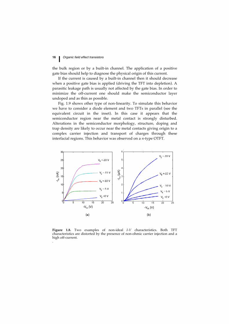
Fig. 1.9 shows other type of non-linearity. To simulate this behavior we have to consider a diode element and two TFTs in parallel (see the equivalent circuit in the inset). In this case it appears that the semiconductor region near the metal contact is strongly disturbed. Alterations in the semiconductor morphology, structure, doping and trap density are likely to occur near the metal contacts giving origin to a complex carrier injection and transport of charges through these interfacial regions. This behavior was observed on a n-type OTFT.
Figure 1.8. Two examples of non-ideal I-V characteristics. Both TFT characteristics are distorted by the presence of non-ohmic carrier injection and a high off-current. .
1.4 Non-ideal characteristics ⎢ 17
Figure 1.9. I-V characteristics observed for an n-type OFET. Severe distortion for low Vds is observed. The inset shows an equivalent circuit to model this behavior.
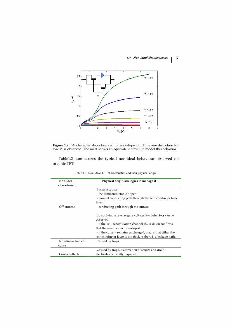
Table1.2 summarizes the typical non-ideal behaviour observed on organic TFTs
.Table 1.1. Non-ideal TFT characteristics and their physical origin.
Non-ideal characteristic
Physical origin/strategies to manage it
Off-current
Possible causes: - the semiconductor is doped. - parallel conducting path through the semiconductor bulk
layer. - conducting path through the surface. By applying a reverse gate voltage two behaviors can be
observed: - if the TFT accumulation channel shuts-down confirms
that the semiconductor is doped. - if the current remains unchanged, means that either the
semiconductor layer is too thick or there is a leakage path. Non-linear transfer
curve Caused by traps.
Contact effects.
Caused by traps. Passivation of source and drain electrodes is usually required.
18 ⎢ Organic field effect transistors
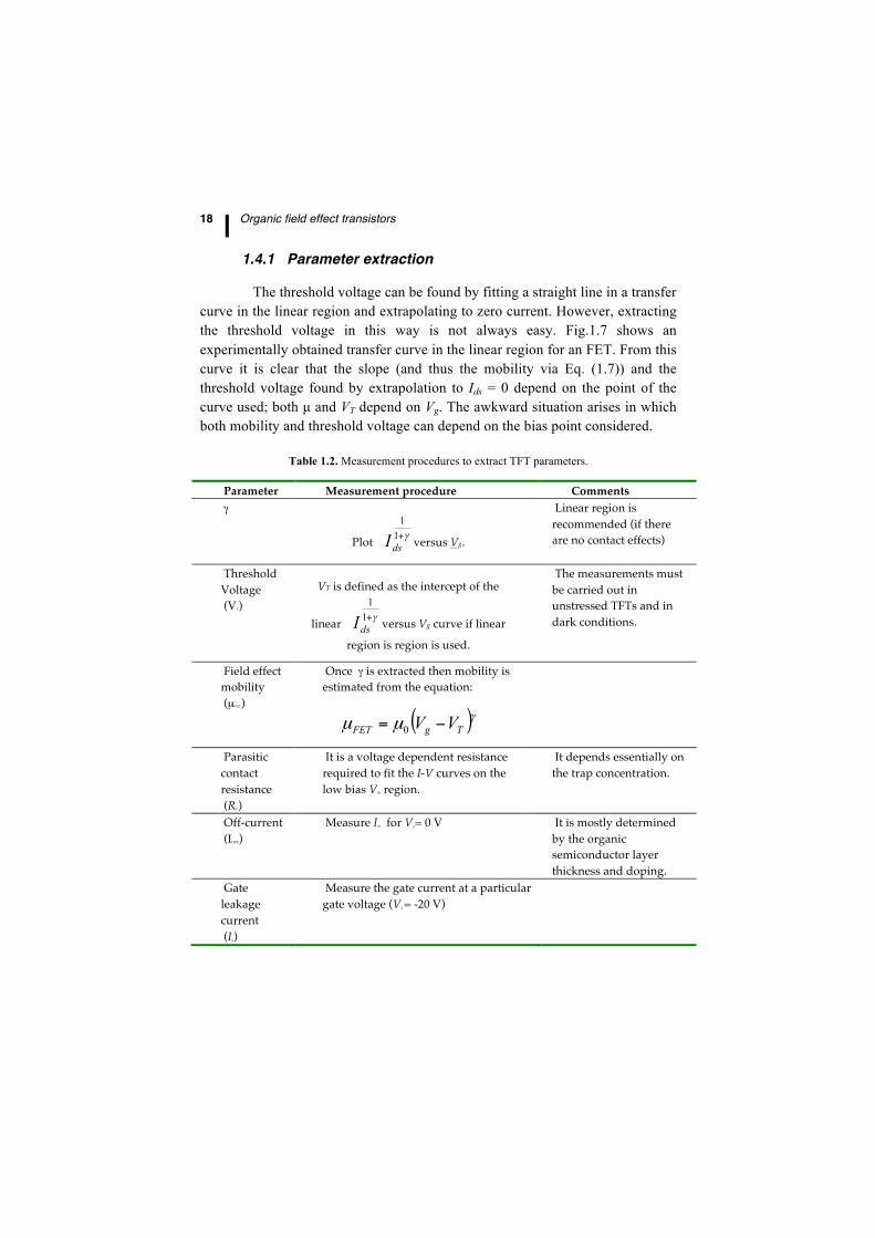
1.4.1 Parameter extraction
The threshold voltage can be found by fitting a straight line in a transfer curve in the linear region and extrapolating to zero current. However, extracting the threshold voltage in this way is not always easy. Fig.1.7 shows an experimentally obtained transfer curve in the linear region for an FET. From this curve it is clear that the slope (and thus the mobility via Eq. (1.7)) and the threshold voltage found by extrapolation to Ids = 0 depend on the point of the curve used; both µ and VT depend on Vg. The awkward situation arises in which both mobility and threshold voltage can depend on the bias point considered.
Table 1.2. Measurement procedures to extract TFT parameters.
Parameter Measurement procedure Comments γ
Plot γ+11
dsI versus Vg.
Linear region is recommended (if there are no contact effects)
Threshold Voltage (VT)
VT is defined as the intercept of the
linear γ+11
dsI versus Vg curve if linear
region is region is used.
The measurements must be carried out in unstressed TFTs and in dark conditions.
Field effect mobility (µFET)
Once γ is extracted then mobility is estimated from the equation:
( )γµµ TgFET VV −= 0
Parasitic contact resistance (RC)
It is a voltage dependent resistance required to fit the I-V curves on the low bias Vds region.
It depends essentially on the trap concentration.
Off-current (IOFF)
Measure Ids for Vg= 0 V It is mostly determined by the organic semiconductor layer thickness and doping.
Gate leakage current (Ig)
Measure the gate current at a particular gate voltage (Vg = -20 V)
1.4 Non-ideal characteristics ⎢ 19
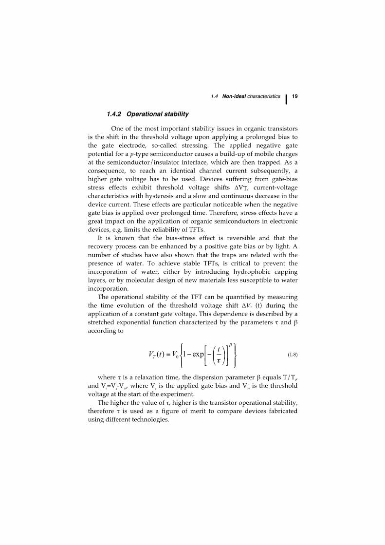
1.4.2 Operational stability
One of the most important stability issues in organic transistors is the shift in the threshold voltage upon applying a prolonged bias to the gate electrode, so-called stressing. The applied negative gate potential for a p-type semiconductor causes a build-up of mobile charges at the semiconductor/insulator interface, which are then trapped. As a consequence, to reach an identical channel current subsequently, a higher gate voltage has to be used. Devices suffering from gate-bias stress effects exhibit threshold voltage shifts ∆VT, current-voltage characteristics with hysteresis and a slow and continuous decrease in the device current. These effects are particular noticeable when the negative gate bias is applied over prolonged time. Therefore, stress effects have a great impact on the application of organic semiconductors in electronic devices, e.g. limits the reliability of TFTs.
It is known that the bias-stress effect is reversible and that the recovery process can be enhanced by a positive gate bias or by light. A number of studies have also shown that the traps are related with the presence of water. To achieve stable TFTs, is critical to prevent the incorporation of water, either by introducing hydrophobic capping layers, or by molecular design of new materials less susceptible to water incorporation.
The operational stability of the TFT can be quantified by measuring the time evolution of the threshold voltage shift ∆VT (t) during the application of a constant gate voltage. This dependence is described by a stretched exponential function characterized by the parameters τ and β according to
⎪⎭
⎪⎬⎫
⎪⎩
⎪⎨⎧
⎥⎦
⎤⎢⎣
⎡⎟⎠
⎞⎜⎝
⎛−−=β
τtVtVT exp1)( 0 (1.8)
where τ is a relaxation time, the dispersion parameter β equals T/T0,
and V0=V
g-V
T0, where V
g is the applied gate bias and VT0 is the threshold
voltage at the start of the experiment. The higher the value of τ, higher is the transistor operational stability,
therefore τ is used as a figure of merit to compare devices fabricated using different technologies.
20 ⎢ Organic field effect transistors
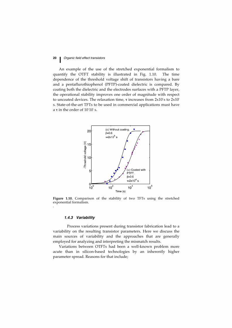
An example of the use of the stretched exponential formalism to
quantify the OTFT stability is illustrated in Fig. 1.10. The time dependence of the threshold voltage shift of transistors having a bare and a pentaflurothiophenol (PFTP)-coated dielectric is compared. By coating both the dielectric and the electrodes surfaces with a PFTP layer, the operational stability improves one order of magnitude with respect to uncoated devices. The relaxation time, τ increases from 2x10³
s to 2x10⁴ s. State-of-the-art TFTs to be used in commercial applications must have a τ in the order of 106
-107 s.
Figure 1.10. Comparison of the stability of two TFTs using the stretched exponential formalism. .
1.4.3 Variability
Process variations present during transistor fabrication lead to a variability on the resulting transistor parameters. Here we discuss the main sources of variability and the approaches that are generally employed for analyzing and interpreting the mismatch results.
Variations between OTFTs had been a well-known problem more acute than in silicon-based technologies by an inherently higher parameter spread. Reasons for that include;
1.4 Non-ideal characteristics ⎢ 21
- irregular morphology of the semiconductor, - difficulty in controlling the precise dimensions of OTFTs, - mobile trapped charges in the dielectric, - uneven material deposition, - roughness of the semiconductor-gate dielectric interface
which leads to mobility variations between the different transistors.
Artefacts, such as bad transistor layout and incorrect data analysis, may also introduce variability.
Interestingly, not all parameters affect the transistor current on the same way. According to Eq. (1.6), variations in the threshold voltage VT affect the saturation current of the transistor quadratically, while variations inµ, W, L, and dOX, influence the saturation current only linearly.
The large transistor variability poses a serious challenge to the cost-effective utilization of organic analogue circuits. It prohibits the use of OFETs in configurations that rely on precisely matched currents, as for instance current-steering D/A converters. Thus, the variability issues are of paramount importance.
Semiconductor foundries run analyses on the variability of attributes of transistors (length, width, dielectric thickness, etc.). This set of files are generally referred to as "model files" in the industry and are used by electronic design assisted (EDA) tools for simulation of transistor and circuit designs. Designers using this approach run simulations to analyze how the outputs of the circuit will behave according to the measured variability of the transistors for that particular process. These simulations allow estimating the final circuit yield, starting from a basic inverter and stepping up towards the full integrated circuit. Moreover, simulations taking into account the area dependent variability increase the predicted yield, as expected.
1.4.3.1 Experimental procedures and methodologies to study variability
Variability characterization requires a large number of measurements on a variety of devices, layout styles, and environments. The methodology used in CMOS technologies to account for local parameter variations and transistor mismatch can be transposed to organic thin-

22 ⎢ Organic field effect transistors
film transistor technologies. For each TFT, an electrical parameter P is characterized by a continuous distribution with space and specific noise power intensity AP independent of the device surface area. Therefore, in the local approach, the variance � of parameter P for a device with surface WL takes the form
WLAp
p
22 =σ (1.9)
For instance, the variance � in the threshold voltage Vt will follow
WLqQ
Cd
OXVt 4
12
2 =σ (1.10)
Where Qd is the channel charge, and COX is the gate oxide capacitance per unit area. Once the extraction has been done, data filtering is usually applied to eliminate erroneous values.
1.4.3.2 Limitations of test structures
Parasitic effects caused by off-current or parasitic fringe current outside the channel region can introduce errors in parameter extraction and lead to an incorrect variability analysis. Next a specific example is discussed.
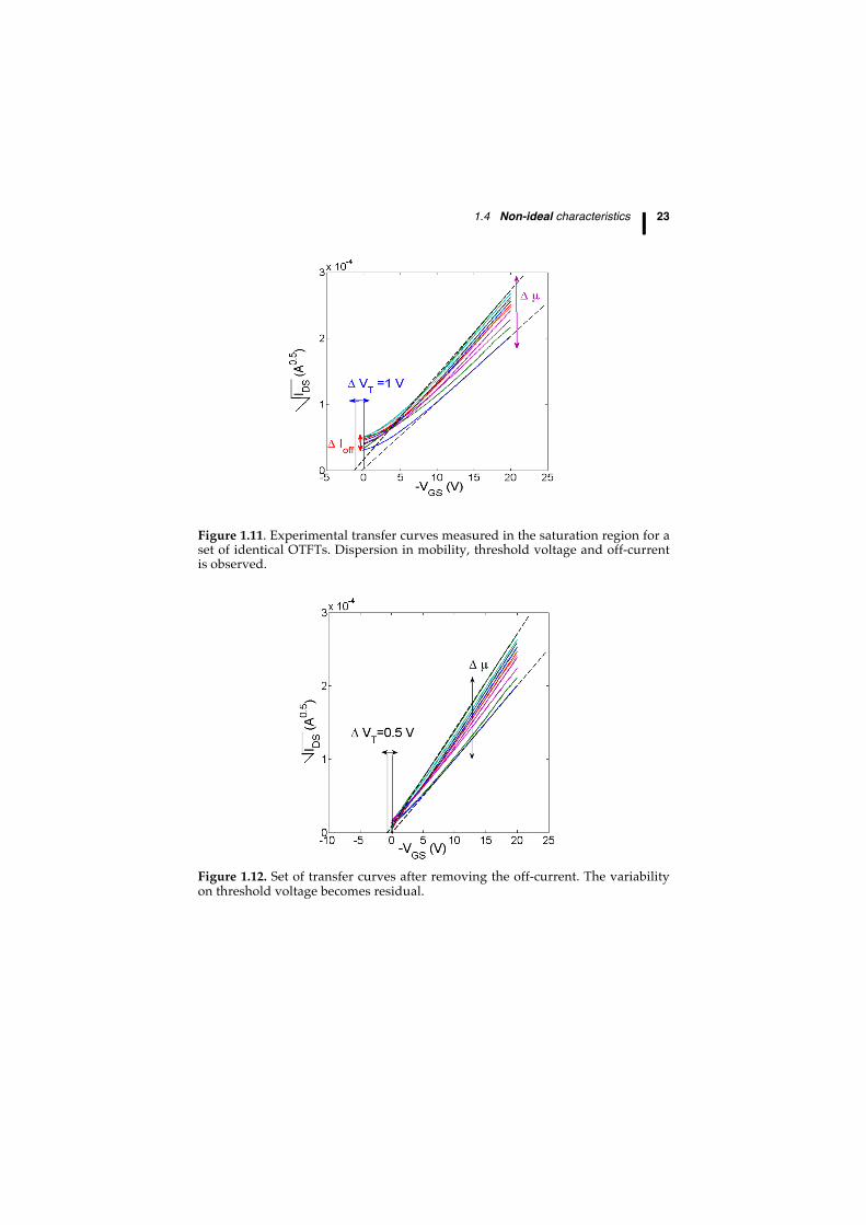
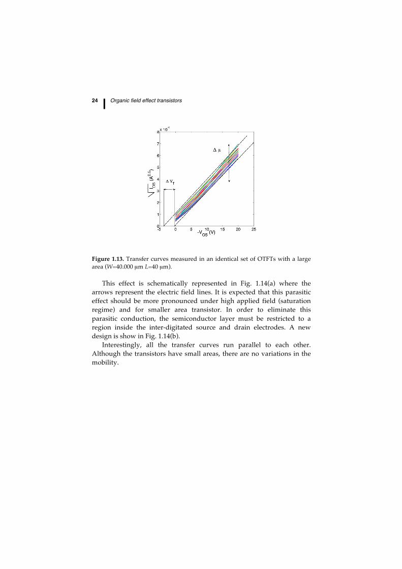
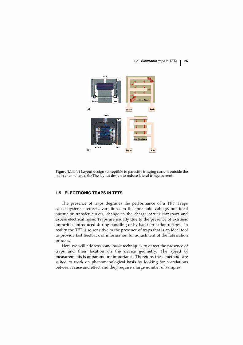
Fig. 1.11 shows a set of transfer curves for small area OTFTs produced in identical conditions and located in the same substrate. Apparently, there are variations in the off-current, in the threshold voltage as well as on the field-effect mobility. When the off-current is removed from all the curves, the variability on the threshold voltage becomes residual. This is shown in Fig. 1.12. However, the application of the same correction procedure to a large area OTFT shows no variations on the mobility. Indeed, all the transfer curves run parallel to each other (see Fig. 1.13). The fact that the dispersion on mobility is dependent on the area of the OTFT, demonstrates conclusively that the variation on mobility arises from the presence of a parasitic source-drain current flowing outside the channel area.
1.4 Non-ideal characteristics ⎢ 23
Figure 1.11. Experimental transfer curves measured in the saturation region for a set of identical OTFTs. Dispersion in mobility, threshold voltage and off-current is observed.
Figure 1.12. Set of transfer curves after removing the off-current. The variability on threshold voltage becomes residual.
24 ⎢ Organic field effect transistors
Figure 1.13. Transfer curves measured in an identical set of OTFTs with a large area (W=40.000 µm L=40 µm).
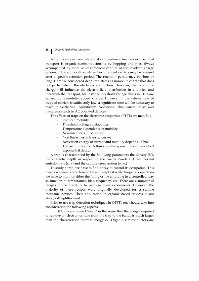
This effect is schematically represented in Fig. 1.14(a) where the arrows represent the electric field lines. It is expected that this parasitic effect should be more pronounced under high applied field (saturation regime) and for smaller area transistor. In order to eliminate this parasitic conduction, the semiconductor layer must be restricted to a region inside the inter-digitated source and drain electrodes. A new design is show in Fig. 1.14(b).
Interestingly, all the transfer curves run parallel to each other. Although the transistors have small areas, there are no variations in the mobility.
1.5 Electronic traps in TFTs ⎢ 25
Figure 1.14. (a) Layout design susceptible to parasitic fringing current outside the main channel area. (b) The layout design to reduce lateral fringe current.
1.5 ELECTRONIC TRAPS IN TFTS
The presence of traps degrades the performance of a TFT. Traps cause hysteresis effects, variations on the threshold voltage, non-ideal output or transfer curves, change in the charge carrier transport and excess electrical noise. Traps are usually due to the presence of extrinsic impurities introduced during handling or by bad fabrication recipes. In reality the TFT is so sensitive to the presence of traps that is an ideal tool to provide fast feedback of information for adjustment of the fabrication process.
Here we will address some basic techniques to detect the presence of traps and their location on the device geometry. The speed of measurements is of paramount importance. Therefore, these methods are suited to work on phenomenological basis by looking for correlations between cause and effect and they require a large number of samples.
26 ⎢ Organic field effect transistors
A trap is an electronic state that can capture a free carrier. Electrical
transport is organic semiconductors is by hopping and it is always accompanied by more or less frequent capture of the involved charge carriers in traps of localized states. Such trapped carriers may be released after a specific retention period. The retention period may be short or long. Here we considered deep trap states as immobile charge that does not participate in the electronic conduction. However, their columbic charge will influence the electric field distribution in a device and therewith the transport, for instance threshold voltage shifts in TFTs are caused by immobile-trapped charge. However if the release rate of trapped carriers is sufficiently low, a significant time will be necessary to reach quasi-thermal equilibrium conditions. This causes delay and hysteresis effects in AC operated devices.
The effects of traps on the electronic properties of TFTs are manifold: - Reduced mobility - Threshold voltages instabilities - Temperature dependence of mobility - Non-linearities in IV curves - Non linearities in transfer curves - Activation energy of current and mobility depends on bias - Transient response follows multi-exponentials or stretched
exponential decays A trap is characterized by the following parameters the density (Nt),
the energetic depth in respect to the carrier bands (Et) the thermal emission rate (en, ep) and the capture cross section (σn, σp)
To study a trap, we have to find a way to control its occupation. This means we must know how to fill and empty it with charge carriers. Then we have to monitor either the filling or the emptying in a controlled way as function of temperature, bias, frequency, etc. There are a number of recipes in the literature to perform these experiments. However, the majority of these recipes were originally developed for crystalline inorganic devices. Their application to organic based devices is not always straightforward.
Prior to use trap detection techniques in OTFTs one should take into consideration the following aspects:
1-Traps are named "deep" in the sense that the energy required to remove an electron or hole from the trap to the bands is much larger than the characteristic thermal energy kT. Organic semiconductors are
1.5 Electronic traps in TFTs ⎢ 27
relatively wide band-gap semiconductors typical around 2 eV. Silicon has a band gap of only 1.1 eV. Therefore, organic semiconductors can accommodate very deep traps. The meaning of a “deep trap” is very different in organic or in silicon technology. A trap of 0.1 eV is considered deep in silicon technology whereas in organic electronics it is considered a shallow trap. A deep trap in organics may have an energetic depth of 0.5-0.8 eV. This has important consequences. While a deep trap in silicon can be filled and emptied in a matter of seconds at room temperature, in an organic material it may take a day to empty. Some techniques to look at deep traps in silicon operate in time scales of seconds or milliseconds. This means they are not applicable for studying traps in organic electronic devices.
2- Traps in organic semiconductors have usually very large cross sections. This means they fill very fast. But because they are deep they empty slowly. Trap filling times are several orders of magnitude faster than emptying times. From a practical point of view, in organic TFTs is easier to study traps during the filling process while in silicon-based devices it is usually standard procedure to study the traps during the emptying process. For silicon based devices the traps are first filled, usually at low temperatures, to prevent a fast escape. This method may be impracticable for organics because of the extremely long times required to monitor a trap release process.
3- In inorganic crystalline devices trapped charge carriers can be de-trapped by interaction with light and the resulting current is recorded as a function of the wavelength of the light. In principle, such an optical stimulated current-spectrum would directly yield the energy distribution of the trap states if an optical transition from a trap state to the transport states is possible. Unfortunately, in many organic semiconductors a direct transition from the trap state to the transport states is not allowed. Usually, the incident light excites the carrier into an excited state of the same molecule, from where a free carrier is generated by auto-ionization. Thus, the required optical transition energy is often not related to the energy difference between trap and transport state.
4- In organic electronics traps are very abundant. Trap concentration often is higher than the free carrier concentration.
This section starts by using the non-ideal TFT characteristics as a simple tool to detect the presence of shallow localized charge density. These basically provide information about the charges that are not totally
28 ⎢ Organic field effect transistors
free but can participate in the electrical conduction. Techniques to look at deep traps (immobile charge) are discussed in the end.
1.5.1 TFT non-ideal characteristics as a tool to measure traps.
Information about the localized trap density can be extracted by measuring how far a TFT transfer curve deviates from the ideal behaviour. Insight into the energetic distribution of these localized charges can be obtained by measuring the temperature dependence of the mobility or the TFT drain-source current. These two cases will be discussed.
1.5.1.1 Extraction of localized charge density from the TFT transfer characteristics
A trap free TFT should have a liner transfer curves or quadratic transfer curve on the linear and in the saturation region respectively. Deviations from this behavior are caused by localized charge. This density of localized charge is then taken into account by the γ parameter as discussed in section 1.4. The γ parameter is related to a characteristic temperature T0 of the density of sates (DOS) by:
220
−=TT
γ (1.11)
T is the absolute temperature and T0 the characteristic temperature. The energy distribution of the DOS gd (E), is expressed as
⎟⎟⎠
⎞⎜⎜⎝
⎛ −=
0
exp)(kTEE
gEg Vdod (1.12)
E is the energy of an electron, gdo the density of states (DOS) of traps at the valence band EV, k Boltzmann’s constant, and T0 a parameter describing the distribution (the slope of a logarithmic plot of the DOS).
γ can be extracted from the transfer curves. This can be done by trial and error or by an integration procedure.
1.5 Electronic traps in TFTs ⎢ 29
( )( )
( )gds
g
V
gds
g VI
dVVIVH
g
∫=
max
0 (1.13)
Using the measured linear transfer characteristics Ids in the integral function, the slope and intercept of H(Vg) are calculated
SlopeInterceptVT = (1.14)
and
21−=
Slopeγ (1.15)
The extraction of γ can be made either from the linear or from the saturation region.
Although, linear region is preferable, bad source and drain metal contacts may cause additional distortion on the linear transfer curve making difficult to extract γ.
1.5.1.2 Temperature dependence of the charge transport
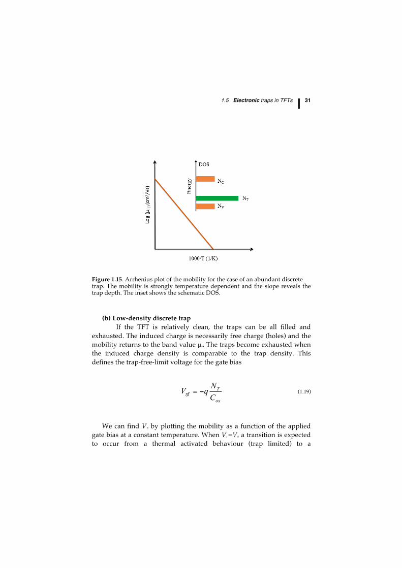
The charge-carrier mobility of MOSFET devices based on silicon are basically independent of temperature. On the other hand, TFTs based on organic materials do normally not show this characteristic. Complicated temperature dependencies are often observed and reported. These are caused by the presence of traps. Here we will show that Arrhenius plots for different biases may serve as a rapid evaluation tool of the quality of the material. More specifically, they give direct insight into the density-of-states governing the conduction. Three basic temperature dependences will be briefly described here, (a) abundant discrete trap, (b) low-density discrete trap, and (c) abundant traps that are distributed in energy. A detailed analysis can be found in the references.

30 ⎢ Organic field effect transistors
(a) Abundant discrete trap In principle a trap free TFT should show a charge carrier mobility
(µFET), that is bias and temperature independent. For this analysis we consider the intrinsic (band) mobility µ
0 to be temperature independent; this may not be necessaryly true, but is a good approximation. When a discrete trap is assumed, the mobility is lowered significantly by the reduced ratio of free-to-total charge, and becomes temperature dependent, but remains independent of bias. The reasoning is as follows: Free holes (p) in the conduction band, originally induced by the gate bias, can be captured by the traps, turning these positively charged. At thermal equilibrium, the ratio of densities of holes and charged traps NT
+
is determined by the energetic distance ET-EV between them, the relative abundance of the levels, NV and NT, respectively, and the temperature T.
⎟⎠
⎞⎜⎝
⎛ −=+ kT
EENN
Np TV
T
V
T
exp (1.16)
The current is only proportional to the free hole density because the trapped states, by definition, do not contribute to current and the density of electrons is insignificant.
qVC
Np goxT =+ + (1.17)
⎟⎠
⎞⎜⎝
⎛ −−=
kTEE
NN VT
T
V exp0µµ (1.18)
The mobility is thermal activated and independent of bias, the slope of the Arrhenius plot reveals the activation energy of mobility, which is then equal to the depth of the trap level, Ea = ET – EV. This behavior is show in Fig. 1.15.
1.5 Electronic traps in TFTs ⎢ 31
Figure 1.15. Arrhenius plot of the mobility for the case of an abundant discrete trap. The mobility is strongly temperature dependent and the slope reveals the trap depth. The inset shows the schematic DOS.
(b) Low-density discrete trap If the TFT is relatively clean, the traps can be all filled and
exhausted. The induced charge is necessarily free charge (holes) and the mobility returns to the band value µ0. The traps become exhausted when the induced charge density is comparable to the trap density. This defines the trap-free-limit voltage for the gate bias
ox
Ttfl C
NqV −= (1.19)
We can find Vtfl by plotting the mobility as a function of the applied gate bias at a constant temperature. When Vg =Vtfl a transition is expected to occur from a thermal activated behaviour (trap limited) to a
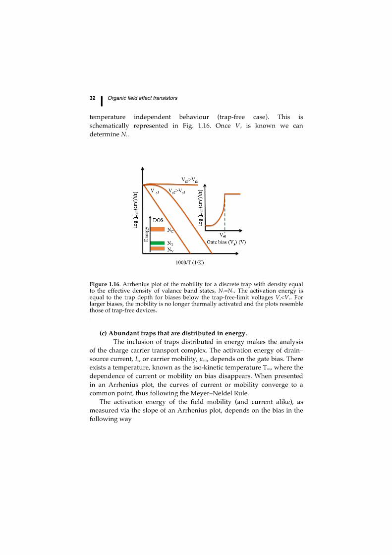
32 ⎢ Organic field effect transistors
temperature independent behaviour (trap-free case). This is schematically represented in Fig. 1.16. Once Vtfl is known we can determine NT.
Figure 1.16. Arrhenius plot of the mobility for a discrete trap with density equal to the effective density of valance band states, NT=NV. The activation energy is equal to the trap depth for biases below the trap-free-limit voltages Vg<Vtfl. For larger biases, the mobility is no longer thermally activated and the plots resemble those of trap-free devices.
.
(c) Abundant traps that are distributed in energy. The inclusion of traps distributed in energy makes the analysis
of the charge carrier transport complex. The activation energy of drain–source current, Ids, or carrier mobility, µFET, depends on the gate bias. There exists a temperature, known as the iso-kinetic temperature TMN, where the dependence of current or mobility on bias disappears. When presented in an Arrhenius plot, the curves of current or mobility converge to a common point, thus following the Meyer–Neldel Rule.
The activation energy of the field mobility (and current alike), as measured via the slope of an Arrhenius plot, depends on the bias in the following way
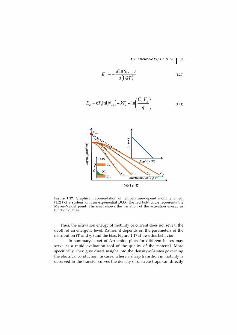
1.5 Electronic traps in TFTs ⎢ 33
( )/kTd
)(µdE FETa 1
ln−= (1.20)
( ) ⎟⎟⎠
⎞⎜⎜⎝
⎛−−=
qVC
kTNkTE goxToa lnln 22 (1.21) (
Figure 1.17. Graphical representation of temperature-depend mobility of eq. (1.21) of a system with an exponential DOS. The red bold circle represents the Meyer-Neldel point. The inset shows the variation of the activation energy as function of bias.
Thus, the activation energy of mobility or current does not reveal the
depth of an energetic level. Rather, it depends on the parameters of the distribution (T2 and gT0) and the bias. Figure 1.17 shows this behavior.
In summary, a set of Arrhenius plots for different biases may serve as a rapid evaluation tool of the quality of the material. More specifically, they give direct insight into the density-of-states governing the electrical conduction. In cases, where a sharp transition in mobility is observed in the transfer curves the density of discrete traps can directly
34 ⎢ Organic field effect transistors
be determined via the trap-free-limit voltage Vtfl, see Eq. (1.19). In organic TFTs the most common situation observed is the corresponding to traps distributed in energy. Arrhenius plots of the current or mobility are straight lines, but the slope (activation energy) depends on the applied gate bias and they do not provide directly the trap depth.
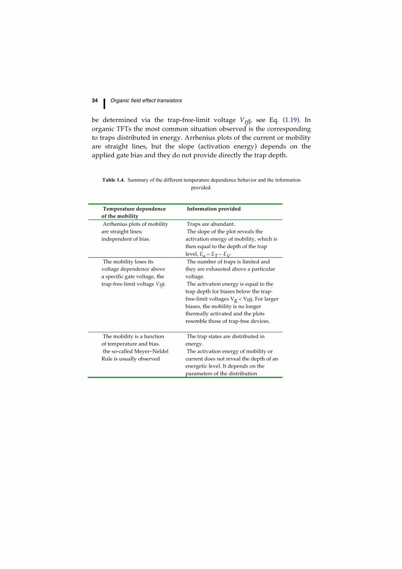
Table 1.4. Summary of the different temperature dependence behavior and the information provided.
Temperature dependence
of the mobility Information provided
Arrhenius plots of mobility are straight lines; independent of bias.
Traps are abundant. The slope of the plot reveals the
activation energy of mobility, which is then equal to the depth of the trap level, Ea = ET – EV
The mobility loses its voltage dependence above a specific gate voltage, the trap-free-limit voltage Vtfl.
The number of traps is limited and they are exhausted above a particular voltage. The activation energy is equal to the
trap depth for biases below the trap-free-limit voltages Vg < Vtfl. For larger biases, the mobility is no longer thermally activated and the plots resemble those of trap-free devices.
The mobility is a function of temperature and bias. the so-called Meyer–Neldel
Rule is usually observed
The trap states are distributed in energy. The activation energy of mobility or
current does not reveal the depth of an energetic level. It depends on the parameters of the distribution
1.5 Electronic traps in TFTs ⎢ 35
1.5.2 Electrical techniques to study traps
There are a number of electrical techniques to study traps. Often these methods require the fabrication of dedicated devices such as Schoktty diodes and metal-insulator-semiconductor (MIS) capacitors. However, in some circumstances TFTs may also be used. Techniques that can be applied to TFTs are the following:
- Small signal impedance spectroscopy (IS) - Thermal stimulated currents (TSC) - Electrical noise
A detailed description of these techniques can be found on the excellent books of Blood and Orton. Here we only briefly describe how to apply them to organic TFTs.
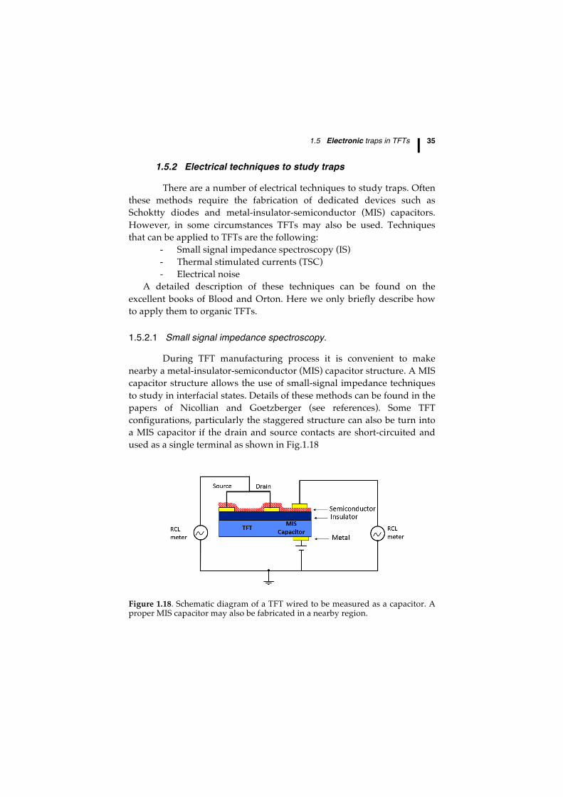
1.5.2.1 Small signal impedance spectroscopy.
During TFT manufacturing process it is convenient to make nearby a metal-insulator-semiconductor (MIS) capacitor structure. A MIS capacitor structure allows the use of small-signal impedance techniques to study in interfacial states. Details of these methods can be found in the papers of Nicollian and Goetzberger (see references). Some TFT configurations, particularly the staggered structure can also be turn into a MIS capacitor if the drain and source contacts are short-circuited and used as a single terminal as shown in Fig.1.18
Figure 1.18. Schematic diagram of a TFT wired to be measured as a capacitor. A proper MIS capacitor may also be fabricated in a nearby region.

36 ⎢ Organic field effect transistors
MIS capacitor can only provide information about interfacial states if
these states can be probed by frequencies below the device relaxation frequency, fR. A MIS-capacitor behaves as a double-layer system. The frequency dependence of the capacitance and resistance shows a dispersion at a particular frequency fR. This frequency must be within a reasonable observation window (10Hz-1MHz) accessible to most of RCL meters or impedance analyzers. To achieve this condition the organic semiconductor layer must have a low resistance.
Once is established that MIS capacitor has a relaxation frequency high enough to perform small-signal measurements, information about interfacial charges can be extracted by measuring the capacitance and the loss for different applied bias and frequencies. The reason for that is because the insulating layer disconnects the interface states from the metal, making them communicate with the semiconductor more readily than with the metal.
The first step is to determine the effect of interface states on the admittance. An ac signal, superimposed on a dc bias will cause the Fermi level to oscillate around a mean position. Any interface states within the modulation depth Vac around this average Fermi level will change their occupancy during an ac cycle and the emitted and captured charges contribute to a capacitance
isis NAqVQC 2=
Δ
Δ= (1.24)
with A the area of the device, q the elementary charge and Nis the density of interface sates per eV per unit area. The charges come out with a characteristic time constant τ. For low frequencies compared to this time constant, the measured capacitance is as given by Eq. (1.24). For increased AC frequencies ɷ, the response of the states to the signal is diminished; the reduced ac current means a reduced measured capacitance. The slower response also causes a phase lag of the ac current and the capacitance can be measured as a conductance and loss, G and G/ɷ, respectively. Standard procedure is to model this with an equivalent circuit of a capacitance in series with a resistance, see Fig. 1.19, in which the capacitance is equal to Cis and the resistance is such that the time constant RC of this circuit is equal to the relaxation time τ of the levels. Note that whereas the capacitance has real physical meaning in this circuit, the resistance only helps to define the time
1.5 Electronic traps in TFTs ⎢ 37
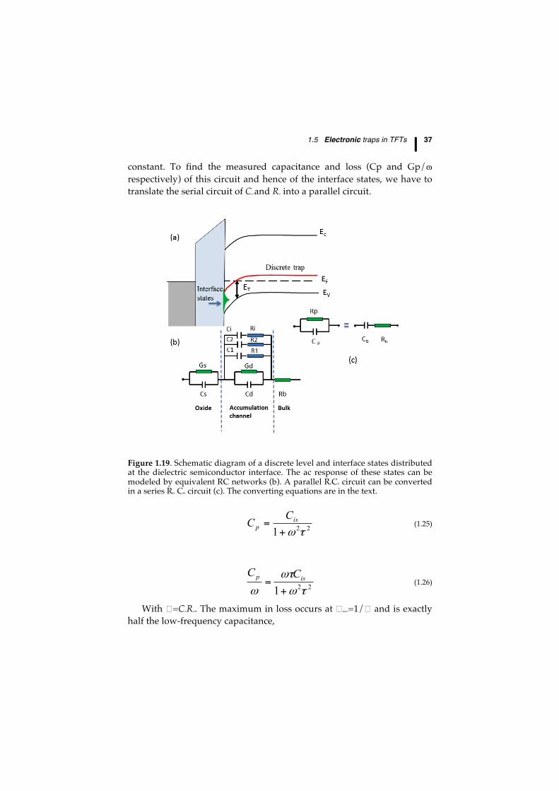
constant. To find the measured capacitance and loss (Cp and Gp/ɷ respectively) of this circuit and hence of the interface states, we have to translate the serial circuit of Cis and Ris into a parallel circuit.
Figure 1.19. Schematic diagram of a discrete level and interface states distributed at the dielectric semiconductor interface. The ac response of these states can be modeled by equivalent RC networks (b). A parallel RPCP circuit can be converted in a series RIS CIS circuit (c). The converting equations are in the text.
221 τω+= is
pCC (1.25)
221 τω
ωτω +
= isp CC (1.26)
With �=CisRis. The maximum in loss occurs at �max=1/� and is exactly half the low-frequency capacitance,
38 ⎢ Organic field effect transistors
22
maxis
p NAqC
=ω
(1.27)
τ
ω1
max = (1.28)
In this way, by measuring the capacitance CP and loss GP/ɷ as a function of frequency, the density of states at a region qVac+kT around the Fermi level can be determined.
The second part of the mapping is the determination of energetic position of the states for which we have just found the density. This can be found by determining the movement of the peak in loss with temperature. The trap relaxation time s follows
⎟⎠
⎞⎜⎝
⎛ −= −
kTEET TTexp2
0ττ (1.29)
with τ0 still depending on the density of states at the top of the valence band, the average thermal velocity of the carriers and the capture cross section, but not depending on the temperature. Combining Eqs. 1.27 and 1.28 learns us that an Arrhenius plot of the maximum in the loss as a function of temperature will yield the activation energy, EA = ET -EV, of that particular bunch of states,
( ) ⎟⎠
⎞⎜⎝
⎛−=kTETT Aexp20
maxmax ωω (1.30)
To find the distribution of interface states in energy we can scan the bias and repeat the above procedure at every step.
A simple capacitance voltage plot can provide the information about the dielectric layer capacitance. The presence of shallow traps can introduce hysteresis or humps in the plots.
The presence of interfaces states can also reveal as a peak in a loss-voltage plot. This peak can be due to a discrete state, or to states distributed in energy. A discrete state will cause a peak that is independent of the applied bias. A broad energetic interface state
1.5 Electronic traps in TFTs ⎢ 39
distributed in energy cause a peak structure that moves to higher frequencies for higher applied bias.
1.5.2.2 Thermal stimulated currents
The presence of trapped charge carriers in TFTs can in principle be confirmed using, thermally stimulated current (TSC) measurements. The traps are filled by applying a bias while the temperature is such that the trapped carriers cannot be freed by the thermal energy. The temperature is then raised linearly. The liberated carriers contribute to the excess current, i.e. the external current minus the leakage current, until they recombine with carriers of opposite type or join the equilibrium charge carrier distribution. This excess current, measured as function of temperature during heating, is called the thermally stimulated current.
For a single trap level, a TSC curve has one maximum whose position depends on capture cross section, heating rate and trap depth. By varying the heating rates the trap depth and capture cross-section can also be determined. Because detrapping currents are extremely small (pico-amps), TSC can only be used with relatively insulating materials. Normally-off or fully depleted TFTs satisfy this requirement. When performing TSC experiments the transistor is connected as a metal-insulator-semiconductor (MIS) capacitor.
The experimental procedure involves the following steps: 1-The trap filling is performed at room temperature. The filling bias
conditions are kept until the TFT is brought to low temperatures low enough that detrapping can be disregarded.
2- At low temperatures the TFT is connected as a capacitor. Drain and source terminals are short. A picommeter measures the capacitor discharging current between the gate terminal and the drain and source terminals.
3-The TFT then is heated at a constant rate, β = dT/dt, up to high temperatures. The trapped carriers are released and collected at the grounded source and drain electrodes. The temperature where a current peak occurs is related to the energetic depth of the trap state and the area under the peak is related to the trap density.
Fig. 1.20 shows TSCs curves recorded using an organic TFT. The figure shows also the base line (a curve recorded without trap filling) to
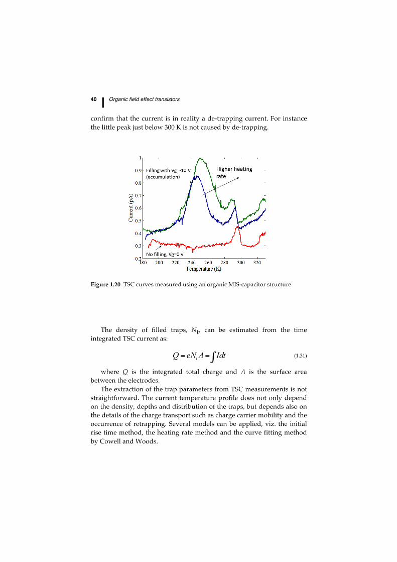
40 ⎢ Organic field effect transistors
confirm that the current is in reality a de-trapping current. For instance the little peak just below 300 K is not caused by de-trapping.
Figure 1.20. TSC curves measured using an organic MIS-capacitor structure.
The density of filled traps, Nt, can be estimated from the time integrated TSC current as:
∫== IdtAeNQ t (1.31)
where Q is the integrated total charge and A is the surface area between the electrodes.
The extraction of the trap parameters from TSC measurements is not straightforward. The current temperature profile does not only depend on the density, depths and distribution of the traps, but depends also on the details of the charge transport such as charge carrier mobility and the occurrence of retrapping. Several models can be applied, viz. the initial rise time method, the heating rate method and the curve fitting method by Cowell and Woods.
1.5 Electronic traps in TFTs ⎢ 41
The initial rise method is valid for all types of recombination kinetics and assumes that the current in the initial part of the curve, when the traps begin to empty, is exponentially dependent on temperature. This method is often used when the full TSC curve cannot be recorded or is distorted by other processes. The method only provides the trap depth and is usually less accurate than the other models.
A more reliable determination of the trap depth is obtained from the relation between the heating rate β and the temperature of the peak maximum, Tm, as described by Blood and Orton in Eq. (1.32):
( ) ⎟⎟
⎠
⎞⎜⎜⎝
⎛+=
⎭⎬⎫
⎩⎨⎧
=σγkE
kTE
TT T
m
T
m
m lnln4
β (1.32)
In which β is the heating rate, ET is the trap depth, k is the Boltzmann constant is the capture cross section and γ is a parameter depending on the effective mass. From a series of TSC curves at different heating rates, the peak temperatures, Tm can be determined. The activation energy of the trap can then be obtained from a linear plot ( )β4
mTln vs. mT1 . The slope yields a value for the activation energy.
Special care has to be taken into account when using TFTs connected as capacitors to perform TSC experiments. Often the bottom electrode is the entire substrate. When a filling bias is applied, it may charge the entire semiconductor area which is larger than the device area. The charges in the vicinity of the TFT can diffuse to the contacts and the leads, where they are collected and measured in the external circuit. The released charges during the TSC curve are extracted from an area larger than that between the TFT electrodes. This may lead to discrepancies between the total charge expected and the measure charge.
Alternatively, it is possible to fit the complete TSC curves numerically using the classical approach of Cowell and Woods. The underlying assumption is monomolecular recombination of the charge carriers from a discrete set of traps with a single trapping level with a trap depth ET below the conduction band, with negligible re-trapping. The current I then follows from:
( )( )( ) offII +ΘΘ−+
Θ−=
− 22exp B1expA
(1.33)
42 ⎢ Organic field effect transistors
In which venA t µτ= , ( )mmT kvEB ΘΘ== exp2β , mT kTE=Θ . Here, nt, is the initial trap density of traps filled, τ is the average
lifetime for a free carrier, µ is the mobility and ν is the attempt to escape frequency. The TSC curves can be fitted with four fitting parameters, Tm, A, ET and Ioff. We note that at high temperatures, when a significant number of traps is emptied, the conductivity of the TFT channel is partially restored and the associated background current severely distorts the measurements. For temperatures above the TSC peak the current cannot be treated solely as a detrapping current and the analysis is usually not possible.
1.6 CIRCUITS AND SYSTEMS
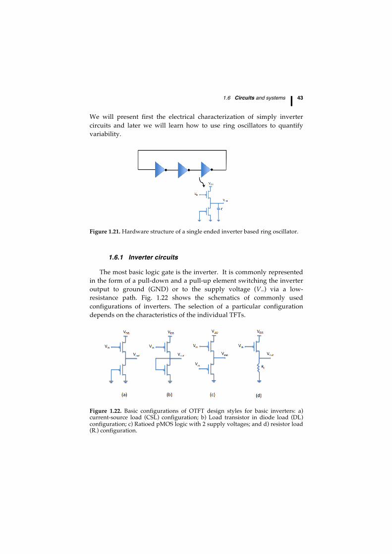
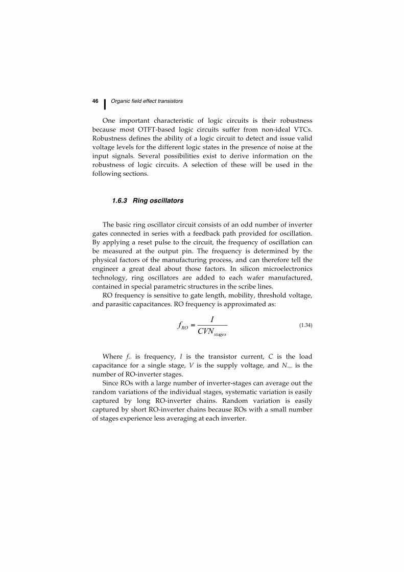
Having studied the electrical performance of individual transistors, it is now important to understand how they behave when connected into circuits. A simple circuit is the inverter. It is based on only two transistors and well suited to prove the capability of organic TFTs to build up more complex circuits. The inverter has to show signal amplification and, most importantly, their output signal has to be able to drive a subsequent inverter stage. The last requirement can be tested with a ring oscillator (RO). This device consists of an odd number of inverters connected with each other in series. Fig. 1.21 shows the principal electronic circuit of a three-stage ring oscillator. A ring oscillator is often used to demonstrate a new technology. In silicon microelectronic circuits many wafers include a ring oscillator as part of the scribe line test structures. They are used during wafer testing to measure the effects of manufacturing process variations.
It is important to emphasize that one should only embark into the process of making circuits when individual TFTs perform reasonable well. Circuits will not work properly if the threshold voltage of individual TFTs is not stable, or if the current modulation ratio is poor. On/off drain current ratios reaching 103-104 are considered as a minimum to obtain suitable digital circuits.
Inverters and ring oscillators may fulfil several objectives, (i) to show that the processing technology is mature enough to fabricate circuits, (ii) to monitor variations caused by systematic and random physical effects.
1.6 Circuits and systems ⎢ 43
We will present first the electrical characterization of simply inverter circuits and later we will learn how to use ring oscillators to quantify variability.
Figure 1.21. Hardware structure of a single ended inverter based ring oscillator.
1.6.1 Inverter circuits
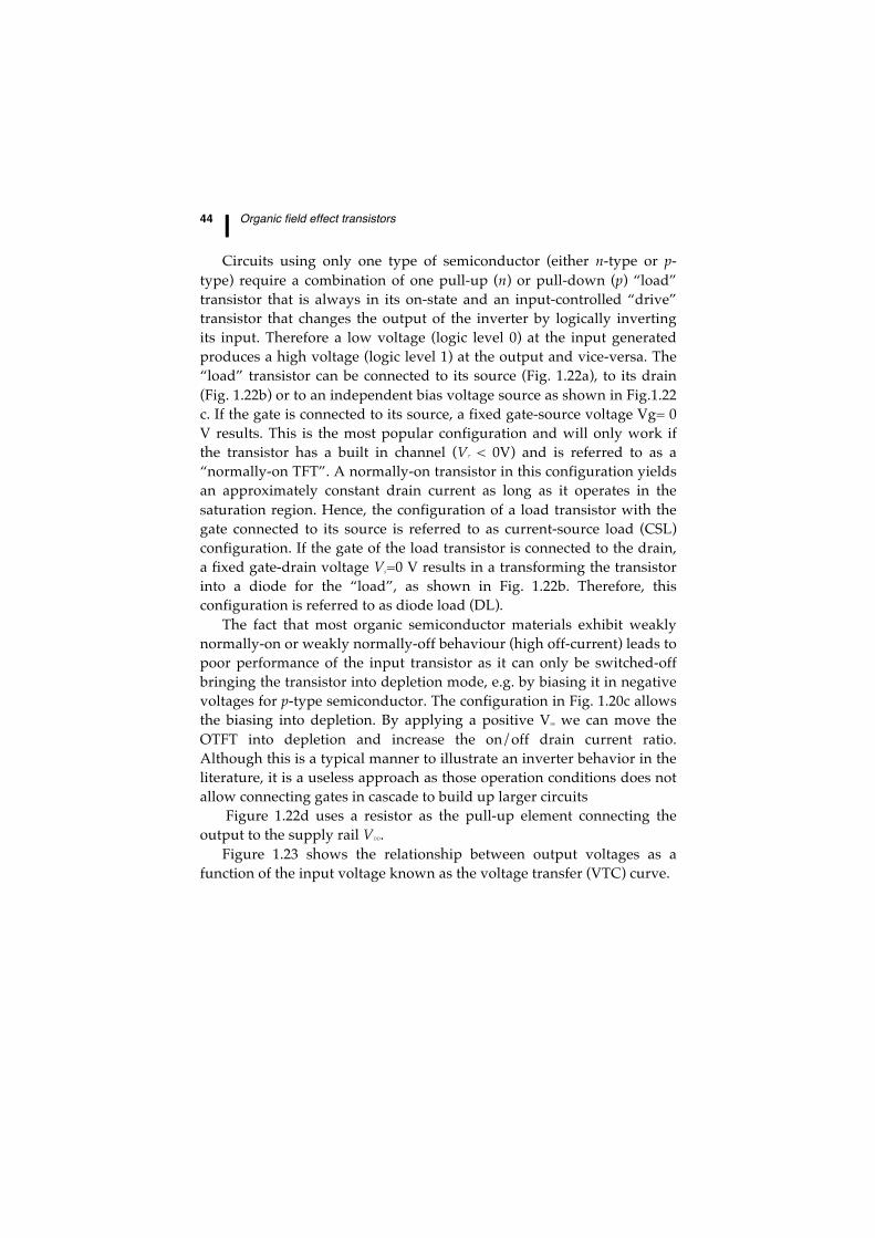
The most basic logic gate is the inverter. It is commonly represented in the form of a pull-down and a pull-up element switching the inverter output to ground (GND) or to the supply voltage (VDD) via a low-resistance path. Fig. 1.22 shows the schematics of commonly used configurations of inverters. The selection of a particular configuration depends on the characteristics of the individual TFTs.
Figure 1.22. Basic configurations of OTFT design styles for basic inverters: a) current-source load (CSL) configuration; b) Load transistor in diode load (DL) configuration; c) Ratioed pMOS logic with 2 supply voltages; and d) resistor load (RL) configuration.
44 ⎢ Organic field effect transistors
Circuits using only one type of semiconductor (either n-type or p-
type) require a combination of one pull-up (n) or pull-down (p) “load” transistor that is always in its on-state and an input-controlled “drive” transistor that changes the output of the inverter by logically inverting its input. Therefore a low voltage (logic level 0) at the input generated produces a high voltage (logic level 1) at the output and vice-versa. The “load” transistor can be connected to its source (Fig. 1.22a), to its drain (Fig. 1.22b) or to an independent bias voltage source as shown in Fig.1.22 c. If the gate is connected to its source, a fixed gate-source voltage Vg= 0 V results. This is the most popular configuration and will only work if the transistor has a built in channel (VT < 0V) and is referred to as a “normally-on TFT”. A normally-on transistor in this configuration yields an approximately constant drain current as long as it operates in the saturation region. Hence, the configuration of a load transistor with the gate connected to its source is referred to as current-source load (CSL) configuration. If the gate of the load transistor is connected to the drain, a fixed gate-drain voltage Vg=0 V results in a transforming the transistor into a diode for the “load”, as shown in Fig. 1.22b. Therefore, this configuration is referred to as diode load (DL).
The fact that most organic semiconductor materials exhibit weakly normally-on or weakly normally-off behaviour (high off-current) leads to poor performance of the input transistor as it can only be switched-off bringing the transistor into depletion mode, e.g. by biasing it in negative voltages for p-type semiconductor. The configuration in Fig. 1.20c allows the biasing into depletion. By applying a positive VSS we can move the OTFT into depletion and increase the on/off drain current ratio. Although this is a typical manner to illustrate an inverter behavior in the literature, it is a useless approach as those operation conditions does not allow connecting gates in cascade to build up larger circuits
Figure 1.22d uses a resistor as the pull-up element connecting the output to the supply rail VDD.
Figure 1.23 shows the relationship between output voltages as a function of the input voltage known as the voltage transfer (VTC) curve.
1.6 Circuits and systems ⎢ 45
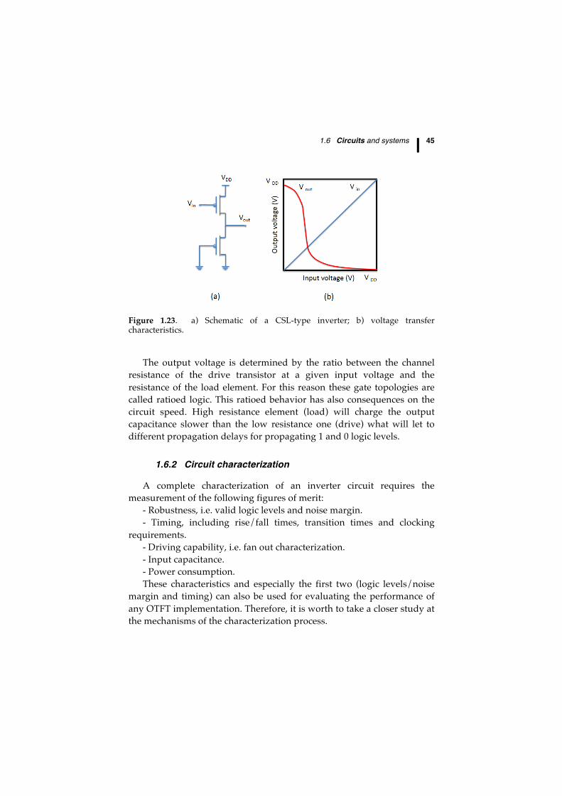
Figure 1.23. a) Schematic of a CSL-type inverter; b) voltage transfer characteristics.
The output voltage is determined by the ratio between the channel resistance of the drive transistor at a given input voltage and the resistance of the load element. For this reason these gate topologies are called ratioed logic. This ratioed behavior has also consequences on the circuit speed. High resistance element (load) will charge the output capacitance slower than the low resistance one (drive) what will let to different propagation delays for propagating 1 and 0 logic levels.
1.6.2 Circuit characterization
A complete characterization of an inverter circuit requires the measurement of the following figures of merit:
- Robustness, i.e. valid logic levels and noise margin. - Timing, including rise/fall times, transition times and clocking
requirements. - Driving capability, i.e. fan out characterization. - Input capacitance. - Power consumption. These characteristics and especially the first two (logic levels/noise
margin and timing) can also be used for evaluating the performance of any OTFT implementation. Therefore, it is worth to take a closer study at the mechanisms of the characterization process.
46 ⎢ Organic field effect transistors
One important characteristic of logic circuits is their robustness
because most OTFT-based logic circuits suffer from non-ideal VTCs. Robustness defines the ability of a logic circuit to detect and issue valid voltage levels for the different logic states in the presence of noise at the input signals. Several possibilities exist to derive information on the robustness of logic circuits. A selection of these will be used in the following sections.
1.6.3 Ring oscillators
The basic ring oscillator circuit consists of an odd number of inverter
gates connected in series with a feedback path provided for oscillation. By applying a reset pulse to the circuit, the frequency of oscillation can be measured at the output pin. The frequency is determined by the physical factors of the manufacturing process, and can therefore tell the engineer a great deal about those factors. In silicon microelectronics technology, ring oscillators are added to each wafer manufactured, contained in special parametric structures in the scribe lines.
RO frequency is sensitive to gate length, mobility, threshold voltage, and parasitic capacitances. RO frequency is approximated as:
stages
RO CVNIf = (1.34)
Where fRO is frequency, I is the transistor current, C is the load
capacitance for a single stage, V is the supply voltage, and Nstages is the number of RO-inverter stages.
Since ROs with a large number of inverter-stages can average out the random variations of the individual stages, systematic variation is easily captured by long RO-inverter chains. Random variation is easily captured by short RO-inverter chains because ROs with a small number of stages experience less averaging at each inverter.
1.7 TFTs FOR BIOMEDICAL applications ⎢ 47
1.6.4 Summary
Electrical properties of the inverter have been presented in the current chapter. The low On/Off drain current ratio is a key issue in the design using pMOS-only logic, as the load transistor is always on, thus reducing output swing.
OTFT stability plays also an important role. Threshold voltage variations affect the noise margins of the logic gates are and the optimal drive/load ratio. Thus high variability can be transformed into a severe limitation of the number of logic gate stage that can be chained. This limits the amount of circuits that can be implemented. Lack of stability also plays an important role in a circuit that use to work in continuous operation.
Since ring oscillators oscillate at a frequency dependent on the characteristics and dimensions of the devices as well as the loads of each inverter, these circuits can be used to detect device and interconnect process variation through measurements on their oscillating frequencies.
1.7 TFTS FOR BIOMEDICAL APPLICATIONS
To use OTFTs as sensors we have to disturb or cause a change in
one or more of the transistor parameters, (i) threshold voltage, (ii) off-current and (i) field-effect mobility. Therefore, TFTs are multi-parameter and amplifying sensing devices. Chemicals, biological substances and even living cells may interact with several parts of the device structure and change the TFT parameters. Basically, there are three different strategies to use a TFT as a sensor:
- Floating gate method. - Changes in the TFT channel or at the channel/contact interfaces. - Changes in the dielectric layer.
1.7.1 Floating gate method.
The floating gate method has been substantially explored on inorganic based TFTs. This method has been used to fabricate neuron-device interfaces as show in Fig.1.24a. Neurons generate small voltage fluctuations on top of the floating gate terminal and modulate the
48 ⎢ Organic field effect transistors
channel current underneath. An identical approach was implemented using organic based TFTs (see Fig.1.24b). However, the TFTs used for this purpose have their channels exposed and do not have a built-in dielectric layer or even a gate terminal, they are a resistor. The gate dielectric will be established only when the device is immersed into the electrolyte and the electrolyte itself plays the role of the gate terminal. This occurs because when conductive or semiconductive materials are immersed into electrolytes a double-layer (Helmholtz layer) is established at the metal/electrolyte interface. This layer has a high capacitance and an associated resistance. The double-layer is conveniently described by a parallel RC network as shown in Fig. 1.24. This electrochemical layer plays the role of dielectric. The capacitance is usually high (µF/cm2) and the associated parallel resistance is in the range of a few kΩ/cm2. Cells generate low frequency signals (f <1 kHz) with amplitude in the microvolts range. These low frequency bioelectrical signals are easily coupled trough the double-layer capacitance (CD) and modulate the TFT channel current.
Bioelectronic organic based devices can make use of a third metal terminal, which is in contact with the electrolyte to modulate the channel conductance. This channel modulation by a DC voltage in an electrolyte medium can be complex. We may assume that ions brought to near the semiconductor/electrolyte surface electrostatically modulate the channel conductance. Or, alternatively, the ions penetrate into the TFT channel causing a chemical oxidation or reduction of the organic semiconductor channel. Independently of the mechanism, these devices show I-V characteristics alike a transistor. As expected, the range of DC voltages that can be applied is limited to voltages below |1V|.
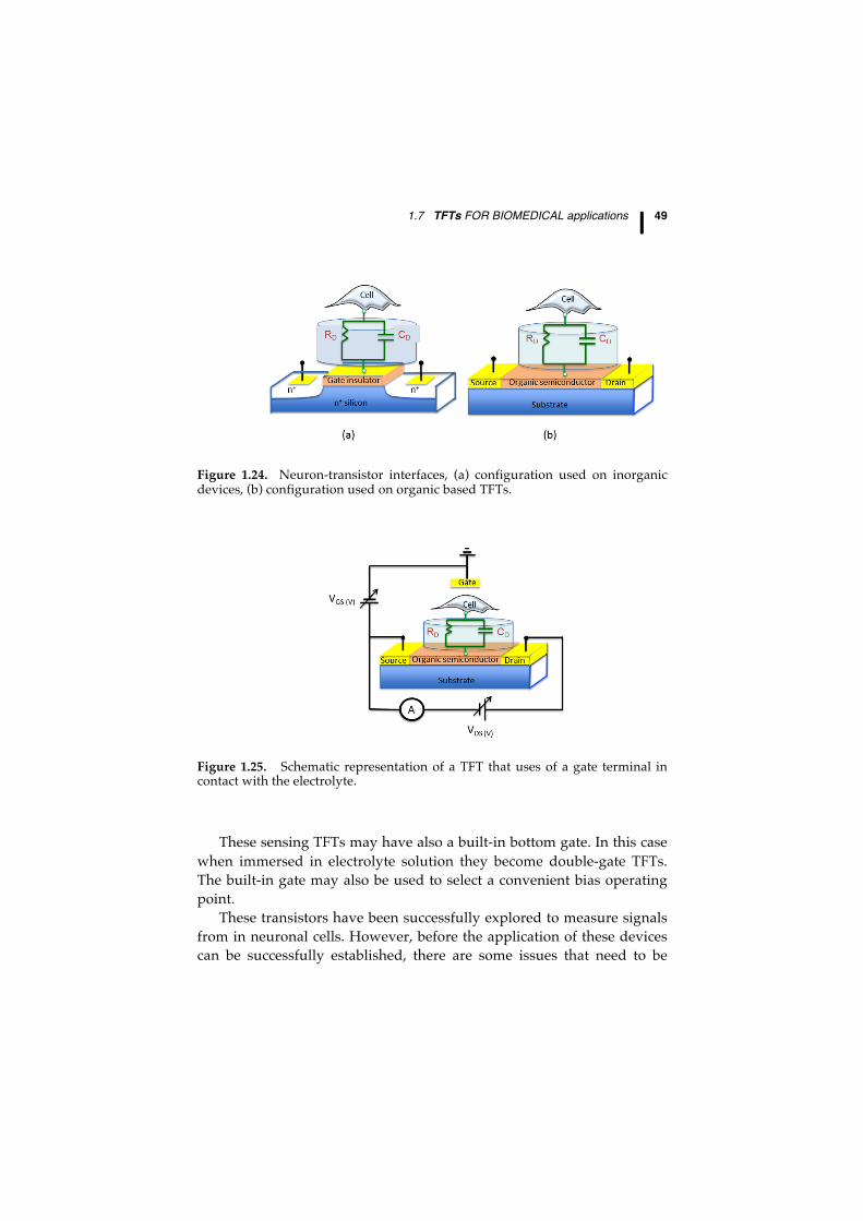
1.7 TFTs FOR BIOMEDICAL applications ⎢ 49
Figure 1.24. Neuron-transistor interfaces, (a) configuration used on inorganic devices, (b) configuration used on organic based TFTs.
Figure 1.25. Schematic representation of a TFT that uses of a gate terminal in contact with the electrolyte.
These sensing TFTs may have also a built-in bottom gate. In this case when immersed in electrolyte solution they become double-gate TFTs. The built-in gate may also be used to select a convenient bias operating point.
These transistors have been successfully explored to measure signals from in neuronal cells. However, before the application of these devices can be successfully established, there are some issues that need to be
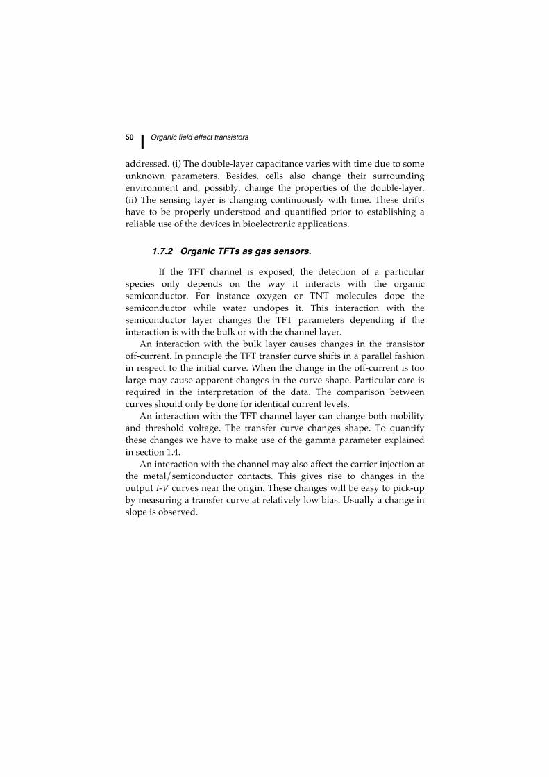
50 ⎢ Organic field effect transistors
addressed. (i) The double-layer capacitance varies with time due to some unknown parameters. Besides, cells also change their surrounding environment and, possibly, change the properties of the double-layer. (ii) The sensing layer is changing continuously with time. These drifts have to be properly understood and quantified prior to establishing a reliable use of the devices in bioelectronic applications.
1.7.2 Organic TFTs as gas sensors.
If the TFT channel is exposed, the detection of a particular species only depends on the way it interacts with the organic semiconductor. For instance oxygen or TNT molecules dope the semiconductor while water undopes it. This interaction with the semiconductor layer changes the TFT parameters depending if the interaction is with the bulk or with the channel layer.
An interaction with the bulk layer causes changes in the transistor off-current. In principle the TFT transfer curve shifts in a parallel fashion in respect to the initial curve. When the change in the off-current is too large may cause apparent changes in the curve shape. Particular care is required in the interpretation of the data. The comparison between curves should only be done for identical current levels.
An interaction with the TFT channel layer can change both mobility and threshold voltage. The transfer curve changes shape. To quantify these changes we have to make use of the gamma parameter explained in section 1.4.
An interaction with the channel may also affect the carrier injection at the metal/semiconductor contacts. This gives rise to changes in the output I-V curves near the origin. These changes will be easy to pick-up by measuring a transfer curve at relatively low bias. Usually a change in slope is observed.
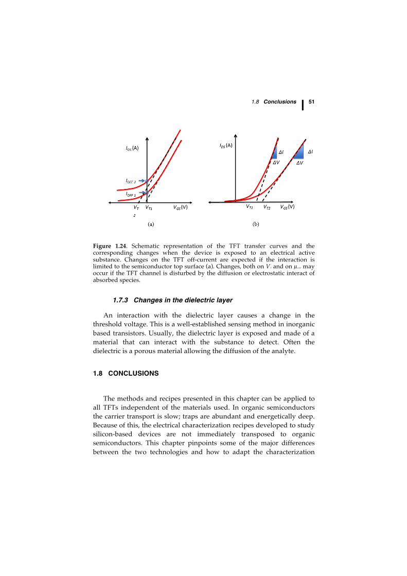
1.8 Conclusions ⎢ 51
Figure 1.24. Schematic representation of the TFT transfer curves and the corresponding changes when the device is exposed to an electrical active substance. Changes on the TFT off-current are expected if the interaction is limited to the semiconductor top surface (a). Changes, both on VT and on µFET may occur if the TFT channel is disturbed by the diffusion or electrostatic interact of absorbed species.
1.7.3 Changes in the dielectric layer
An interaction with the dielectric layer causes a change in the threshold voltage. This is a well-established sensing method in inorganic based transistors. Usually, the dielectric layer is exposed and made of a material that can interact with the substance to detect. Often the dielectric is a porous material allowing the diffusion of the analyte.
1.8 CONCLUSIONS
The methods and recipes presented in this chapter can be applied to
all TFTs independent of the materials used. In organic semiconductors the carrier transport is slow; traps are abundant and energetically deep. Because of this, the electrical characterization recipes developed to study silicon-based devices are not immediately transposed to organic semiconductors. This chapter pinpoints some of the major differences between the two technologies and how to adapt the characterization
52 ⎢ Organic field effect transistors
methods developed for silicon devices to TFTs based on organic semiconductors. Using the experience gained from the a-Si:H TFT, important progresses have been made in understanding of basic device physics. Influences of the semiconductor band structure, gate dielectric defects, interface density of states, etc. on TFT characteristics, lifetime, failure mechanism, etc. are now understood. This knowledge allows us to use the TFT as a powerful evaluation tool for new materials and new manufacturing technologies. There are constant efforts in searching for new types of organic molecules and polymers to improve performance or to lower the production costs.
Nowadays, the major challenge faced by organic TFTs is reliability, especially deterioration of the device characteristics with time. In this context, the methods presented in this chapter to measure traps and interfacial states are a crucial part of the characterization work.
The TFT is a versatile solid-state transistor configuration that can be applied to a wide range of products. It is difficult to predict in which areas or products, organic TFTs will have big impact in the future. The key impact areas are assumed to be the following:
(i) Flexible electronics. Organic TFTs formed on bendable substrates, can be used in light-
weight, unbreakable, flexible OLED displays on plastic substrates. (ii) Simple circuits. With the transistor performance that is available today a wide range
of applications can already be addressed, in particular, simple logic, memory, and I/O circuits integrated with chemical and biological sensors.
(iii) Sensors, detectors and bioelectronics interfaces. TFTs can be easily modified or connected to other devices to detect or
generate changes of chemical, biological, optical, magnetic, radioactive, and other properties through controlling the transport of charge carriers, etc.
Still remain many fundamental research challenges that need to be addressed and but it appears likely that organic TFTs will find several niche applications.
1.9 Questions ⎢ 53
1.9 QUESTIONS
1-The definition of VT from conventional MOSFETs does not apply to OFETs. What is the practical utility of this parameter?
Answer VT is not an intrinsic TFT parameter. It is physically related with the
presence of traps. The extraction of VT form the transfer curves may be used to quantify the density of traps and the operational stability.
2- Charge carrier mobility can be estimated using Hall effect, time-of-
flight or from space charge limited current (SCLC) measurements. How mobility values extracted from these techniques compare with mobility values extracted by measuring TFT transfer curves?
Answer The mobility determined by Hall effect or time of flight methods
reflect the charge carrier transport through the bulk material and it is usually higher than the field effect mobility extracted using a TFT structure. Scattering centers at the interface control the mobility in a TFT. It depends on the quality of the interface and on the dielectric used.
3-The mobility can be extracted from a linear fit of the gate voltage
dependence of the current in the linear regime or the square root of the current in the saturation regime. However, questions arise when the device exhibits deviations from this ideal behavior. Summarize the common issues encountered and the strategies to circumvent them.
Answer Three sources of non-ideal behavior are often encountered: (i) Device characteristics exhibit hysteresis with the current being
higher on the forward sweep towards than on the reverse sweep. This is usually due to the current degrading on the timescale of the electrical measurement, and this instability reflects charge trapping. If the sweep rate is increased to mask this instability, this can lead to overestimated
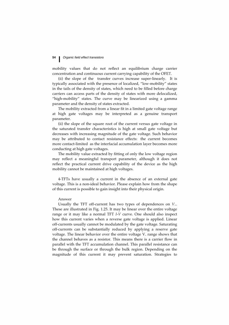
54 ⎢ Organic field effect transistors
mobility values that do not reflect an equilibrium charge carrier concentration and continuous current carrying capability of the OFET.
(ii) the slope of the transfer curves increase super-linearly. It is typically associated with the presence of localized, “low-mobility” states in the tails of the density of states, which need to be filled before charge carriers can access parts of the density of states with more delocalized, “high-mobility” states. The curve may be linearized using a gamma parameter and the density of states extracted.
The mobility extracted from a linear fit in a limited gate voltage range at high gate voltages may be interpreted as a genuine transport parameter.
(ii) the slope of the square root of the current versus gate voltage in the saturated transfer characteristics is high at small gate voltage but decreases with increasing magnitude of the gate voltage. Such behavior maybe attributed to contact resistance effects: the current becomes more contact-limitedas the interfacial accumulation layer becomes more conducting at high gate voltages.
The mobility value extracted by fitting of only the low voltage region may reflect a meaningful transport parameter, although it does not reflect the practical current drive capability of the device as the high mobility cannot be maintained at high voltages.
4-TFTs have usually a current in the absence of an external gate
voltage. This is a non-ideal behavior. Please explain how from the shape of this current is possible to gain insight into their physical origin.
Answer Usually the TFT off-current has two types of dependences on VDS.
These are illustrated in Fig. 1.25. It may be linear over the entire voltage range or it may like a normal TFT I-V curve. One should also inspect how this current varies when a reverse gate voltage is applied. Linear off-currents usually cannot be modulated by the gate voltage. Saturating off-currents can be substantially reduced by applying a reserve gate voltage. The linear behavior over the entire voltage Vds range shows that the channel behaves as a resistor. This means there is a carrier flow in parallel with the TFT accumulation channel. This parallel resistance can be through the surface or through the bulk region. Depending on the magnitude of this current it may prevent saturation. Strategies to
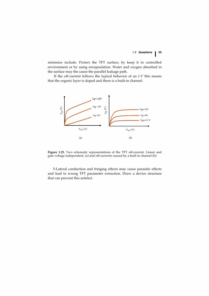
1.9 Questions ⎢ 55
minimize include. Protect the TFT surface; by keep it in controlled environment or by using encapsulation. Water and oxygen absorbed in the surface may the cause the parallel leakage path.
If the off-current follows the typical behavior of an I-V this means that the organic layer is doped and there is a built-in channel.
Figure 1.25. Two schematic representations of the TFT off-current. Linear and gate voltage independent, (a) and off-currents caused by a built in channel (b).
5-Lateral conduction and fringing effects may cause parasitic effects
and lead to wrong TFT parameter extraction. Draw a device structure that can prevent this artefact.
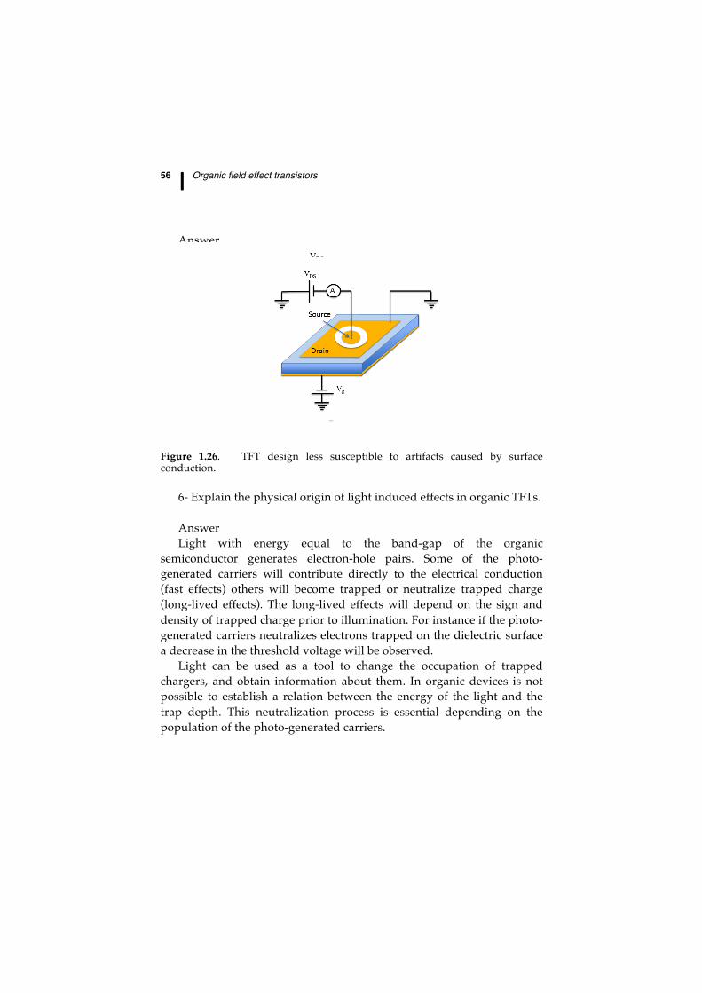
56 ⎢ Organic field effect transistors
Answer
Figure 1.26. TFT design less susceptible to artifacts caused by surface conduction.
6- Explain the physical origin of light induced effects in organic TFTs. Answer Light with energy equal to the band-gap of the organic
semiconductor generates electron-hole pairs. Some of the photo-generated carriers will contribute directly to the electrical conduction (fast effects) others will become trapped or neutralize trapped charge (long-lived effects). The long-lived effects will depend on the sign and density of trapped charge prior to illumination. For instance if the photo-generated carriers neutralizes electrons trapped on the dielectric surface a decrease in the threshold voltage will be observed.
Light can be used as a tool to change the occupation of trapped chargers, and obtain information about them. In organic devices is not possible to establish a relation between the energy of the light and the trap depth. This neutralization process is essential depending on the population of the photo-generated carriers.
1.9 Questions ⎢ 57
7- Outline some strategies to improve TFT operational stability.
Answer
The quality of the dielectric/semiconductor interface determines if the TFT will work or not. A high mobility organic semiconductor deposited in a contaminated dielectric surface will not make a working TFT. It is crucial to select a proper dielectric and handle it carefully. Water is the most difficult contaminant to remove from dielectric surfaces. Even using vacuum processing techniques is always present. The best strategy is to passivate the dielectric surface using ultrathin hydrophobic layers.
. 8-TFTs are multi-parameter sensing devices. Outline some strategies
as well as some precautions when using TFT parameters in sensing applications. Answer
In sensing applications the device is either monitored continuously or periodically. The prolonged application of bias usually causes drifts and changes for instance in the VT not related with the presence of the substance to detect. It is important to devise a method where intrinsic device instabilities are not measured. For instance the device is only switch-on for short periods of time and left resting for long periods of time to allow recovering. An interesting alternative is to use small-signal impedance techniques. Oscillating small fields at low frequencies can be used to monitor the TFT channel resistance and conductance using LCR meters or impedance analyzers. These methods usually do not cause drifts in the properties of TFTs.
9- OTFTs are low current and high impedance devices. Outline some
precautions required to perform the dynamic characterization of an inverter circuit.
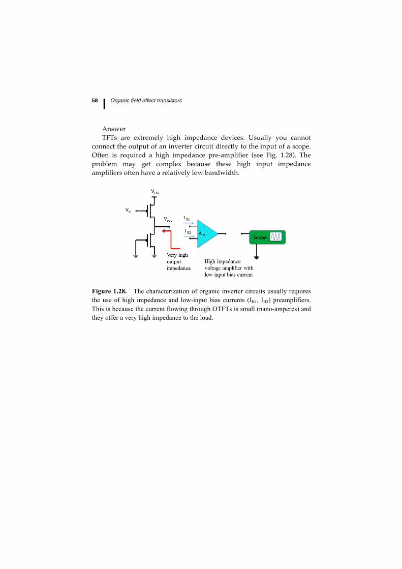
58 ⎢ Organic field effect transistors
Answer TFTs are extremely high impedance devices. Usually you cannot
connect the output of an inverter circuit directly to the input of a scope. Often is required a high impedance pre-amplifier (see Fig. 1.28). The problem may get complex because these high input impedance amplifiers often have a relatively low bandwidth.
Figure 1.28. The characterization of organic inverter circuits usually requires the use of high impedance and low-input bias currents (IB1, IB2) preamplifiers. This is because the current flowing through OTFTs is small (nano-amperes) and they offer a very high impedance to the load.
1.9 Questions ⎢ 59
.
Suggested further reading references
Journal references 1. Braga, D. and Horowitz, G. (2009). High-Performance Organic Field-Effect
Transistors. Adv. Mater., 21, pp. 1473–1486. 2. Campana, A. et al. (000), Electrocardiographic recording with conformable organic
electrochemical transistor fabricated on resorbable bioscaffold, Adv. Mat. 26, pp. 3874-3878.
3. Cowell, T.A.T. and Woods, J. (1967). The evaluation of thermally stimulated current curves, Brit. J. Appl. Phys. 18, pp. 1045-1051.
4. Cramer, T. et al. (2013). Water-gated organic field effect transistors–opportunities for biochemical sensing and extracellular signal transduction, Journal of Materials Chemistry B 1, pp. 3728-3741.
5. Cramer, T. et al. (2013) Organic ultra-thin film transistors with a liquid gate for extracellular stimulation and recording of electric activity of stem cell-derived neuronal networks, Physical Chemistry Chemical Physics, 15, pp. 3897-3905.
6. Feng, C. Marinov, O, Deen, M. J. Selvaganapathy, P. R. and Wu, Y. (2015) 7. Sensitivity of the threshold voltage of organic thin-film transistors to light and water,
J. of Appl. Phys. 117, pp. 185501. 8. Gomes, H. L., et al. (2004). Bias-induced threshold voltages shifts in thin-film
organic transistors, Appl. Phys. Lett. 84, pp. 3184-3186. 9. Gomes, H. L. et al. (2006). Electrical instabilities in organic semiconductors caused
by trapped supercooled water, Appl. Phys. Lett., 88. pp. 08210. 10. Gomes, H. L. et al. (2005). Electrical characterization of organic based transistors:
stability issues, Polymers for Advanced Technologies, 16, pp. 227-231. 11. Horowitz, G. (1988). Organic Field-Effect Transistors, Adv. Mater., 10, pp 365-377. 12. Horowitz, G. (2011). The organic transistor: state-of-the-art and outlook, The
European Physical Journal Applied Physics, 53, 33602. 13. Magliulo, M. et al. (2013). Electrolyte-Gated Organic Field-Effect Transistor
Sensors Based on Supported Biotinylated Phospholipid Bilayer, Adv. Mater., 25, pp. 2090–2094.
14. Marinov, O., Deen, M. J., Zschieschang, U., Klauk, H. (2009). Organic thin-film transistors: Part I—Compact DC modeling Electron Devices, IEEE Transactions on 56, pp. 2952-2961.
15. Marinov, O. Deen, M. J., Iniguez, B. (2005). Charge transport in organic and polymer thin-film transistors: recent issues Circuits, Devices and Systems, IEE Proceedings. 152, pp. 189-209.
60 ⎢ Organic field effect transistors
16. Mathijssen, S. G. J. et al. (2007). Dynamics of threshold voltage shifts in organic
and amorphous silicon field-effect transistors, Adv. Mater.,19, pp. 2785. 17. Nicollia, E. H. and Goetzberger, A. (1967). Bell Syst. Tech. J. 46, pp. 1055-1133. 18. Kim, C. H. et al. (2014). Compact DC Modeling of Organic Field-Effect Transistors:
Review and Perspectives, IEEE transactions on Electron Devices, 61, pp. 278-287. 19. Kim C. H. et al. (2013). A Compact Model for Organic Field-Effect Transistors with
Improved Output Asymptotic Behaviors IEEE Transactions on Electron Devices 60, pp. 1136-1141.
20. Kumar, B., Kaushik, B. K. and Negi, Y. S. (2013). Static and dynamic analysis of organic and hybrid inverter circuits, J. Comput. Electron. 12, pp.765–774.
21. Sirringhaus, H. (2014). 25th Anniversary Article: Organic Field-Effect Transistors: The Path Beyond Amorphous Silicon, Adv. Mater., 26, pp. 1319–1335.
22. Sirringhaus, H. (2009). Reliability of Organic Field-Effect Transistors. Adv. Mater., 21, pp. 3859–3873.
23. Stallinga, P and Gomes, H. L. (2008). Modeling electrical characteristics of thin-film field-effect transistors III. Normally-on devices," Synthetic Metals, 158, pp. 473-478.
24. Stallinga, P. and Gomes, H. L. (2007), "Metal contacts in thin-film transistors," Organic Electronics, 8, pp. 300-304.
25. Stallinga, P. and Gomes, H. L. (2006). Modeling electrical characteristics of thin-film field-effect transistors I. Trap-free materials," Synthetic Metals, 156, pp. 1305-1315. Book references
26. Nicollian, E. H. and Brews, J. R. (1982). MOS (Metal Oxide Semiconductor) Physics and Technology, Wiley, New York.
27. Blood, P. and Orton, J. W. (1992) The Electrical Characterization of Semiconductors: Majority Carriers and Electron States (Techniques of Physics), Academic Press, New York.
1.9 Questions ⎢ 61
List of symbols
ϕm Metal work-function ɷ Angular frequency q Absolute electron charge T Absolute temperature k Boltzmann’s constant NT
+ Charged traps T0 Characteristic temperature of the density of sates G Conductance Vds Drain–source voltage β Dispersion parameter P Device parameter γ Deviation of a transfer curve from the ideal behavior fR. Device relaxation frequency, Nis Density of interface sates per eV per unit area gd(E), Energy distribution of the DOS Vfb Flat-band voltage µFET Field effect mobility p Free hole concentration Ig Gate Leakage current Vg Gate–source voltage COX Gate oxide capacitance per unit area. V
T0 Initial the threshold voltage
TMN Iso-kinetic temperature (Meyer–Neldel) Ei Intrinsic Fermi level G/ɷ Loss Nt Number of traps AP Noise power intensity of parameter distribution dox Oxide thickness εox Permittivity of the insulator material ϕb Potential difference between the Fermi level and the intrinsic
Fermi level Ei RC Parasitic contact resistance τ Relaxation time fRO Ring oscillator frequency Eg Semiconductor bandgap Qd TFT channel charge V
T Threshold voltage W TFT channel width L TFT channel length IOFF TFT off-current µ0 Trap free field effect mobility
62 ⎢ Organic field effect transistors
Nt Trap energetic depth in respect to the carrier bands en, ep Trap thermal emission rate (for electrons and holes) σn, σp Trap capture cross section (for electrons and holes) σ Variance Vtfl The trap-free-limit voltage