OPTIMIZED SILICON SOLAR CELLS FINAL REPORT NOVEMBER 30, 1971 · OPTIMIZED SILICON SOLAR CELLS FOR...
102
I ' OPTIMIZED SILICON SOLAR CELLS FOR SPACE EXPLORATION POWER SYSTEMS FINAL REPORT NOVEMBER 30, 1971 Prepared by Peter A.' lIes JPL Contract No. 952865 Centralab Semiconductor Division Globe-Union Inc. 4501 North Arden Drive El Monte, California 91734 .------- - ---- -N72-22044 ICELLS FOR SPACE EXPLORATI . Inc) I PA lIes (Globe-Un10n, • 1 Final RepoI:t •• __ CSCL 10A 30 Nov. 1971 101 P /\' '-,' \'JJ C- ----_ .. -- - - --- ------'--- https://ntrs.nasa.gov/search.jsp?R=19720014394 2018-06-01T15:19:29+00:00Z
Transcript of OPTIMIZED SILICON SOLAR CELLS FINAL REPORT NOVEMBER 30, 1971 · OPTIMIZED SILICON SOLAR CELLS FOR...
I '
OPTIMIZED SILICON SOLAR CELLS
FOR
SPACE EXPLORATION POWER SYSTEMS
FINAL REPORT
NOVEMBER 30, 1971
Prepared by Peter A.' lIes
JPL Contract No. 952865
Centralab Semiconductor DivisionGlobe-Union Inc.
4501 North Arden DriveEl Monte, California 91734
.------- --~-~------ ---- -N72-22044
«N-AS-A-CR~126216) OPTIMIZ~~- ~~~~O~y~~i~~ICELLS FOR SPACE EXPLORATI . Inc)I P A lIes (Globe-Un10n, •1Final RepoI:t •• __ ,'~ CSCL 10A30 Nov. 1971 101 P /\' '-,' \'JJ
C -----_ .. -- ~---- -~-- ---- ------'---
https://ntrs.nasa.gov/search.jsp?R=19720014394 2018-06-01T15:19:29+00:00Z

OPTIMIZED SILICON SOLAR CELLS
FOR
SPACE EXPLORATION POWER SYSTEMS
FINAL REPORT
NOVEMBER 30, 1971
Prepared by Peter A.' lIes
JPL Contract No. 952865
Centralab Semiconductor DivisionGlobe-Union Inc.
4501 North Arden DriveEl Monte, California 91734
I

A B S T R ACT
This report describes a program aimed at designing andfabricating improved silicon solar cells for a range ofmissions extending from 0.1 to 15 astronomical units(Mercury to Jupiter).
Theoretical analysis was combined with some previousempirical measurements to design cells for five specificplanetary missions.
For missions lying inside Earthradiua (Mercury, Venus)the major cell property required was very low seriesresistance, allowing high curve fill factor to be maintained at the higher intensities. For the Mercury mission,the temperature of the cell had to be kept low. This wasachieved by reflecting more of the incident sunlight byuse of large area front contacts.
Theoretical estimates showed no advantage in shifting thereflectivity minimum of the anti-reflection coating tolonger wavelengths. optimum grid patterns were derivedand used.
For the outer missions (Mars, the Asteroid belts andJupiter) the formation of a Schottky barrier at the backcontact had to be avoided (by use of a P+ layer under theback contact) and the excess leakage current of the PNjunction had to be reduced. This reduction involvedadjustment of several fabrication parameters and was themost difficult to ensure. When these two problems wereminimized, the CFF of the cells remained high for operationat the low temperatures and intensities. Optimum gridpatterns were also derived and used for these missions.
A parallel approach was followed, wherein widely separatedvalues of four cell: variables were combined in a matrixarrangement, and the cells measured over the whole rangeof missions to see if some of the combinations showedpromise for specific missions.
Following the theoretical analysis, eleven groups of cellswere fabricated, at least two groups being specificallydesigned for each of the five target missions. Also, thesixteen matrix groups were fabricated. Later, seven groupsof deliverable cells were fabricated, including at leastone group intended for each target mission.

/
Testing and analysis of all groups was performed at 28°C.This testing included I-V curves at three differentintensities (5, 140, 850 mW/cm ), dark forward and reverseI-V characteristics, and spectral response measurements.
The planned measurements at simulated mission conditionshave not yet been made, thus preventing final conclusionsfrom being made. These measurements will be performedsubsequent to this report, and the results will bereported separately.

1.01.11.21.31.41.51.61.71.82.02.12.22.33.03.13.24.04.14.24.35.05.15.25.36.06.17.08.09.0
10.0
TABLE OF CONTENTS
ABSTRACTList of TablesList of FiguresGLOSSARY
SununaryProgram ObjectivesTheoretical AnalysisMission-Designed Cell FabricationMatrix Cell FabricationCell MeasurementsFabrication of Deliverable CellsConclusionsSignificant Program DevelopmentsIntroductionDocument OrganizationPurpose and ObjectivesBackground to ProgramProgram PlanProgram TasksProgram ChangesAnalytical Study of Optimized DesignNear-Sun MissionOuter MissionsTrade Studies of AnalysisFabrication PhaseFabrication of Mission Design CellsFabrication of Matrix CellsFabrication of Deliverable Cell GroupsMeasurementsMeasurement FacilitiesConclusionsSuggestions for Future Cell Design WorkReferencesBibliography
Appendix A - Special Test Conditions
page No.
(i)(ii)(iii)
111444556777899
121313355455555559626276787981
87

Table No.
1.
2.
3.
4.
5.
6.
7.
8.
9.
10.
11.
12.
13.
14.
15.
16.
17.
List of Tables
Title
Cell parameters for Mission Design Cells
Calculated Equilibrium Temperatures
Relative Power at various Irradiancesand Temperatures
output Power vs. Fraction of Cell Covered
optimum Grid Numbers for Mercury Cells
optimum Grid Numbers for Venus Cells
Temperature and Relative Power forVarious SiO Thicknesses
optimum Grid Numbers for Mars Cells
Optimum Grid Numbers for Asteroid Belt Cells
Optimum Grid Numbers for Jupiter Cells
Effects of Decreasing Intensity for Cellsat 28°C
Onset Temperatures for Cell Degradation
Description of Mission Design Cells
Description of Matrix Cell Groups
Description of Deliverable Cell Groups
Summary of I-V Measurements at 28°C - MissionDesign Cell Groups
Summary of I-V Measurements at 28°C Matrix Cells
(i)
page
3
14
17
21
22
23
29
35
36
36
37
50
56
58
61
63 - 65
70 - 72

Figure No.
1.
2.
3.
4.
5.
6.
7.
8.
9.
10.
11.
LIST OF FIGURES
Title Page
Typical I-V Characteristics as a Function 16of Solar Irradiation at ConstantTemperature
Relative Power vs. Irradiance and Temperature 19
Coefficient of Power Equation vs. Temperature 20
Four Grid Mercury Cell 24
Checkerboard Contact Mercury Cell 25
Grid Pattern for Venus Cell 26
Refractive Indices vs. Wavelength (Si & SiO) 32
Anti-reflection Coating Characteristics 32
Open Circuit Voltage vs. Temperature 41
Effect of Decreased ~emperature on 43Cutoff Wavelength
Optical Absorption Coefficient vs. 44Wavelength for Silicon
12.
13.
14.
15.
16.
17.
18.
Light Generated Current Density vs.Diffusion Length
CFF vs. Series Resistance for VariousValues of Saturation Current Density
Effects of Excess Diode Current orSchottky Barrier on Cell I-V Curve
Grid Designs used for Various MissionDesign Cell Groups
Grid Designs for Mercury Mission
Dark Diode Characteristics forMission Design Cells
Ratio of Readings in Long WavelengthChannel to Reading in Short WavelengthChannel
(ii)
45
47
48
57
60
68
69

19.
20.
Dark Diode Characterist1cs for Matrix Cells
Isc (AM=O) forD1creasing Junction Depth
\ \
74
75

GLOSSARY OF TERMS USED
The following terms are used frequently in solar cell work.The definitions generally accepted in this work are given below.
1. AMO (Air Mass Zero)Refers to the intensity of sunlight measured near to spaceconditions (very low air mass between the sun and the measurement point). The solar spectrum used with AMO sunlight isthat published by Johnson (F. S. Johnson, liThe Solar Constant"J. Meteorol, Vol. 11, p. 431, 1954).
2. Cell parametersThese are the physical properties of the silicon, the contactsor the coating. They are determined by the fabrication sequenceused.
3. Curve Fill Factor (CFF)See item 7. below.
4. DiffusionUsed in two senses. First, it describes the solid state processwhereby impurities are introduced into the silicon, generally toform a layer of conductivity sign opposite to that of the starting silicon. Second, it describes the motion of current carrierswithout the presence of an electrical field. In this secondsense, it also occurs in the definition of the "diffusion length"of the carriers, i.e., the mean distance the carriers travelby diffusion.
5. EfficiencyThe percentage of input solar radiation which is converted bythe solar cell to useful electrical energy.
Efficiency(%) = cell output x 100solar input for total area (including
contacts)
6. Evaporation MasksContacts and coatings for solar cells are generally applied bythermal evaporation in vacuo. The areas where these contactsor coatings are required are defined by shadow masks, withappropriate openings, held in close contact with the solarcell surface during evaporation.
7. I-V CharacteristicsThe numbers used to define the current-voltage output from asolar cell. The output is measured as a continuous curve(traced by varying the load resistance from zero to infinity)in the fourth quadrant of the complete I-V curve. The mostoften used terms are:
Short Circuit Current (Is )The current generated by €he incident light when thecell terminals are shorted.
(iii)

Open Circuit voltage (Voc )The voltage developed by the light at the open terminalsof the cell.
Maximum Power (Pmax )The maximum product of load current times load voltage. Thecorresponding values of load current and voltage are designated Ima~ and Vmax . Often for convenience in large scaletests, cells are graded according to the current at a testvoltage close to Vmax, e.g., for 10 ohm-cm resistivity,current is measured at 430 mV (I430)
Curve Fill Facto¥ (CFF)Prnax expressed as a fraction of the power given by theproduct Isc. V~c
CFF = Pmax~=:..:...._--
I sc Voc
8. IntensityThe term specifying the amount of solar e~ergy incident on thecell. The units generally used are mW/cm •
9. Junction (PN)The dividing region between the shallow surface layer and thestarting silicon. The PN junction is a rectifier (diode) andis necessary for the conversion process of sunlight intoelectrical energy.
10. Junction DepthThe thickness of the shallow surface layer on a solar cell. Thisdepth is generally low, typically 0.5 urn.
11. N or P SiliconSilicon can be doped with impurities to give either N (negative)or P (positive) type of conductivity. The addition of subscriptse.g., N+ or P+ is used to show that regions are heavily dopedwith the impurities.
12. PhotovoltaicThe developing of a voltage (electrical) by a photon (light) input.
13. RadiationA term covering the particles (electrons, protons or neutrons)or electromagnetic radiation (ultraviolet, X-Rays) which thesolar cells encounter in space missions.
14. Radiation ResistanceA qualitative term describing how well solar cells can withstandthe exposure to radiation. The term can be made quantitative bydefining the percentage of output power remaining after a givendosage by a specified radiation.
(iv)

15. Saturation CurrentThe theoretical current associated with the diode created by thePN junction. Ideally, it is the current collected by the junctionfrom carriers generated by thermal processes at the cell operatingtemperature.
16. Schottky Barrier ,A potential barrier arising at the interface between a metal anda semiconductor, such as silicon. It is named after the Germanscientist who first explained these barriers.
17 •. Sheet ResistanceThe resistance of a unit square of a thin layeras the surface layer of silicon in solar cells.on the sheet thickness (junction depth) and thetion in the surface layer.
of material suchIt depends both
carrier concentra-
~
18. Solar SimulatorA test setup which illuminates solar cells by the solar spectrumfor specific missions. The defining parameters are the spe2trum(AMO for space sunlight) and the intensity (e.g., 140 mW/cm fornear-earth, 5 mW/cm2 for near-Jupiter.)
(v)

1.0 SUMMARY
1.1 Program Objectives
The contract objective was to develop silicon solar cellsfor use on spacecraft missions covering a heliocentricorbit range of 0.1 to 15 astronomical units.
The purpose of the program was to exploit the presentstate-of-the-art variables available for Nip siliconsolar cells. These variables are the base resistivityof the P-silicon, the PN junction depth, the sheet resistance, the grid contact configuration, the contact metalsand the coating. The variables were to be combined infabricating cells designed for five specific missions,namely for orbits near Mercury, Venus, Mars, the Asteroidbelts and Jupiter.
Probable operating conditions were chosen for each of thefive orbits. From these conditions, cell designs weredetermined, using a combination of contemporary solarcell theory and previous measurements on cells designedto operate within this range of orbits.
Using these mission designs, a fabrication sequence waschosen for the cells, and groups of cells were fabricated.These mission design cells were intended for measur~ment
at conditions simulating the various missions, and t~ir
performance compared to that of two groups of "controlcells" made according to the best present near-Earthoptimized cells.
In addition to the mission design cells, an alternateapproach was included, aimed at finding cells with goodperformance at some of the five target missions. Thisalternate approach used a sixteen-position matrix of celldesigns, combining fairly wide ranges of four cellfabrication variables, namely bulk resistivity, PNjunction depth, back contact metals and the number ofgrid contacts.
1.2 Theoretical Analysis
The first part of the program was theoretical analysis.Using the solar intensity expected near the various orbitsand making plausible assumptions, the equilibrium temperatures were calculated.
Analysis was made of the solar cell properties at thevarious combinations of intensity and temperature. Thisanalysis was based on three sources, namely, presentsolar cell theory, published theoretical analyses ofvarious missions and practical cell measurements covering some of the range of interest. These latter measurements were needed to provide guidelines for cell
- 1 -
parameter variations which were not predictable from thetheoretical analysis. The results of the analysis areincorporated in Table 1 which specifies the variouscell parameters chosen for the cells designed for thefive missions. The parameters used for optimum nearEarth orbits are also included.
1.2.1 Design of Cells for the Inner Missions (Mercury, Venus)
The design problems resolved to reducing the total seriesresistance of the cell to very low levels to reduce parasitic losses from the large generated currents. Keycell parameters were chosen to ensure low. series resistance. Thus low resistivity silicon (.~1.0 ohm-cm) wasused, a deeper PN junction (- 0.7~m) with correspondinglower sheet resistance (rV 20 ohm/square) and grid configurations providing good current pickup. In addition,in order to keep the cell operating temperature low, alarge sacrifice in possible output was needed. Thetemperature reduction resulted from use of front surface(grid) contacts which reflected a large portion of theinput power. For example, for Mercury cells, 60% of theincident power was reflected, leaving less than half thenormal active cell area.
A theoretical analysis showed no overall advantage inshifting the maximum of the reflectivity curve by increasing the thickness of the antireflection coating.
1.2.2 Design of Cells for the Outer Missions (Mars, Asteroidbelts, Jupiter)
For these missions, the lower solar intensity leads tolower cell temperatures than for Earth orbits and theinner orbits. In addition, the power loss due to seriesresistance is significantly reduced because of the lowercurrent generated. The two main causes for cell powerloss are:
(a) Possibility of a.Schottky voltage barrier at theback surface interface between the P-silicon andthe contact metals. This barrier is most likelyto form at lower temperatures, i.e., it is moreserious as the spacecraft sun distance increases.
(b) Excess leakage currents in the PN junction. Thesecurrents can arise for several reasons duringprocessing. These reasons include surface preparation damage, diffusion-induced strains, introduction of harmful impurities, or damage frommechanical handling.
The practical solution to (a) was to include a P+ layeron the P-silicon, to minimize the chance of forming aSchottky barrier. This P+ layer was provided by both
-2-

TA
BL
E1
CE
LL
PAR
AM
ETER
SFO
RM
ISS
ION
-DE
SIG
NC
EL
LS
An
ti-
Ju
ncti
on
Sh
eet
Fro
nt
Bac
kG
rid
*R
efl
ecti
ve
Mis
sio
nR
esis
tiv
ity
Dep
thR
esis
tan
ce
Co
nta
ct
Co
nta
ct
Co
nfi
cg
ura
tio
nC
oati
ng
Co
mm
ents
(oh
m-c
m)
(11m
)(o
hm
/sq
)
Merc
ury
0.8
-1.5
0.6
20
Ti-
Ag
Ti-
Ag
Ch
eck
erb
oard
SiO
Mu
sth
av
eo
r4
wid
elo
wseri
es
gri
ds
resis
tan
ce
Can
co
nn
ec'
toan
yed
g,
Ven
us
0.8
-1.5
0.5
25
Ti-
Ag
Ti-
Ag
10
gri
ds
SiO
Mu
sth
av
elo
wseri
es
resis
tan
ce
Eart
h0
.8-1
.50
.43
3T
i-A
gT
i-A
g6
gri
ds
SiO
7-1
40
.44
5T
i-A
gT
i-A
g6
gri
ds
SiO
Mar
s1
-30
.62
0T
i-A
gP
+w
ith
4g
rid
sS
iOT
i-A
g
Aste
roid
3-7
1.0
15
Ti-
Ag
P+
wit
h2
gri
ds
SiO
Nee
dex
tra
Belt
sT
i-A
gcare
inp
rep
ara
tio
of
fro
nt
su
rface
an
ed
ges,
an
din
co
nta
ct
sin
teri
ng
.
Ju
pit
er
3-7
1.0
15
Ti-
Ag
P+
wit
h1
gri
dS
iON
eed
ex
tra
Ti-
Ag
care
inp
rep
ara
tio
of
fro
nt
su
rface
an
ed
ges,
an
din
co
nta
ct
sin
teri
ng
.
Gri
dP
att
ern
ssh
ow
nin
Fig
ure
s1
5,
16
-3-

P+ diffusion or by alloying of aluminum. The lattermethod was more convenient, and was adopted.
There was no such ready solution to (b). Extreme carewas needed in silicon surface preparation, in diffusiontechniques, and in the handling steps. Also, care wastaken to reduce the sintering temperature time cycle toprevent the chance of punch-through of the PN junctionby the contact metals. In addition, higher resistivitysilicon (3-7 ohm-ern) was used because the PN junctionquality could be higher. Deeper junctions were used toafford additional protection from surface leakage.
The grid contact analysis, although not so important, wasextended to these outer missions and the optimum numberof grids for Mars, the Asteroid belts, and Jupiter werederived as four, two and one, respectively.
1.2.3 Solder Coverage
It was considered best for all missions to reduce theamount of solder used, or preferably to eliminate italtogether on the cells. This is practical becauseseveral interconnecting methods are available which donot require solder on the cells.
1.3 Mission-Design Cell Fabrication
Based on the parameters in Table 1, the starting silicon,diffusion, contact and coating parameters were controlledand.combined to give cells designed for the five missions.Cell groups are described in Section 5.1 below. A totalof 1300 cells was made for these groups.
1.4 Matrix Cell Fabrication
Sixteen groups of cells were made using extreme values ofresistivity (0.1 and 10 ohm-cm), junction depth (0.4 and1.6~m) combined with two grid configurations (zero or six)and two back contact structures. The matrix scheme isgiven below in Section 5.2.
As described below, the first matrix cells were accidentally mixed during fabrication. A second run was made forall sixteen groups. For both runs, a total of 3200 cellswas made, with 100 control cells.
1.5 Cell Measurements
The cells described above were measured at 28°C under thefollowing illumination conditions:
(a)
(b)
(c)
2140 mW/cm , AMO spectrum
25 mW/ern , AMO spectrum (used a perforated box asneutral filter)
850 mw/cm2 , Tungsten Iodide illumination-4-

Cell Measurements (continued)
(d) Dark (zero illumination) forward diode characteristics
(e) Dark (zero illumination) reverse diode characteristics
(f) Typical spectral response at 28°C
The results of these measurements are given in Section6.2 below.
In addition, typical cells from each group were to bemeasured at:
(i)
(ii)
2850 mW/cm , cell approximately 100°C
25 mW/cm , cell at -140°C
(iii) Dark forward diode characteristics, -140°C
As explained below, these latter measurements were notperformed. They will be completed after this report,and the results will be reported separately.
1.6 Fabrication of Deliverable Cells
Based on the measurements, the final design for cellsoptimized for five missions was decided, and the deliverable cells (5 groups, 50 cells) were fabricated. Thesecell groups are described in section 5.3 below. Twoadditional groups were added and are described. For theseseven groups at least 1400 cells were fabricated.
1.7 Conclusions
The program, including theoretical analysis, cell fabrication, and analysis for 28°C measurements, led to conclusions which were incorporated in the cells designed forthe target missions, and are described above.
Final conclusions will be made separately from this report,based on simulated mission measurements to be made in thefuture.
Some general conclusions are possible, as follows:
(1) Present-day cell processing techniques can be variedand combined to give cells theoretically capable of goodoperation for the target missions. The outermissions presented more difficulty in cell design.
-5-

(2) There lS often unexpected interaction betweencell fabrication steps when these are varied overfairly wide range. Such interactions must beunderstood and minimized before the separateeffects of these variations can be found. Presentmethods used to analyze cell·properties are adequateto explore these interactions.
(3) The precise blend of cell parameters cannot befinalized without taking into account all themission requirements.
1.8 Significant Program Development
The current literature and previous measurements wereincorporated into the theoretical analysis. This analysisshowed that present range of available cell parametersshould give cells designed for the fiv.e target missions.The cell fabrication steps showed reasonable trends incell properties measured at 28°C. It also appeared thatcurrently available analytical methods (combining photovoltaic I-V characteristics, dark I-V characteristics,spectral response and physical measurements) are adequateto check the effects of the variations in cell processingsteps. The program provided relatively large samples(up to 100 per group) in about thirty cell groups covering a wide range of parameters. These cells will add toexisting cell measurement information.
The development not completed when this report was writtenwas the final simulated mission evaluation and analysis.This phase will be completed in the future and the resultswill be reported separately.

2.0 INTRODUCTION
2.1 Document Organization
This report consists of the following major parts:
(a) A summary (Section 1.0) of the program objectives,the work accomplished, and the conslusions drawn.
(b) Background material (Section 2.0) to explain theProgram chosen.
(c) The detailed work plan (Section 3.0).
(d) A theoretical analysis (Section 4.0) of cellperformance over the range of expected conditions.
(e) Fabrication details of optimized cells (Section 5.0).
(f) Details of measurements made (Section 6.0), andanalysis of these measurements.
(g) Conclusions drawn (Section 7.0).
(h) Suggestions for future work (Section 8.0).
(i) References (Section 9.0).
(j) A bibliography of pertinent references, with notes.(Section 10.0)
(k) Appendix A, describing the special test equipment.
2.2 Purpose and Objectives
The purpose of the program was to exploit the presentstate-of-the-art for NIP silicon solar cells to designand fabricate cells optimized for each of five separatemissions covering the range of orbits near Mercury (to0.1 astronomical units) out to near Jupiter (to 15 astronomical units).
Five specific missions, namely near the orbits of Merc~ry,
Venus, Mars, the asteroid belts and Jupiter, were chosenas specific targets.
-7-

The objectives of the program were to survey previouswork, to combine these results with present understanding of silicon solar cell operation, and to designspecific cells optimized for the five missions. Following fabrication of the cells, detailed measurements andanalysis were performed, and conclusions drawn as to theeffectiveness of the program.
2.3 Background to Program
Most silicon solar cells fabricated have been optimizedfor near-earth orbits. Thus they perform well at intensities around 140 mW/cm2 , and cell temperatures from 10to 60°C. Some modification in cell design (often drastic)is required when designing for orbits with intensities aslow as 5 mW/cm2 and temperatures around -140°C, or forintensities up to 850 mW/cm2 , and ceLl temperatures around100°C. Cells designed specifically for these extremes(Jupiter and Mercury missions) have been built and analyzed.However, it was thought profitable to examine the wholerange of missions over Which the importance of variouscontrollable cell parameters could change and to combinethese parameters to give cells optimized for the fivemissions under study.
At the outset, it was agreed that all of the necessaryarray systems requirements e.g. low weight, and low costcould not be included in this study. However, the cellsdesigned are comparable to present systems suggested forthese missions and in a few cases (e. g. light weight,large area arrays for Jupiter) any advancements in arraydesign could probably include the cell improvementssuggested in the present program.
No allowance was made for radiation resistance. In thecase of the inner missions, nearer the sun, the onlyradiation of concern is sporadic solar flares, and thesecan be partly dealt with by combination of transparentshielding (covers) and by the chance of accelerated annealingat higher cell operating temperatures. For the outermissions, the main problem is from the Jovian radiation belts,and no ready solution exists for the suspected intenseirradiation at low cell temperatures, While maintaining thelow weight of a large area array.
-8-

Previous related work on cell parameter measurementswithin the present range of interest is summarized bylisting the references, with notes on the highlightsof the conclusions drawn. In some cases the workreferenced is proceeding simultaneously with the presentprogram.
3.0 PROGRAM PLAN
3.1 Program Tasks
The tasks accomplished in the program arose from workoutlined in the preceding sections. These tasks aresummarized in the following sections.
3.11
3.12
Analysis Phase
Most of the pertinent literature references were readand information considered useful for the present program was extracted. A list of these references withnotes is given in SectionlD.O below. In addition tothese published results, in-house measurements atCentralab Semiconductor were analyzed over the range ofinterest. These measurements showed how conventionalcells begin to lose their effectiveness as the extremesof high or low solar intensity were approached. Basedon the conclusions from these previous measurements,current solar cell theory was used to derive designswhich should give optimum performance at the varioustarget missions.
Cell Fabrication Phase
The fabrication sequence was similar to that used for conventional cell manufacture except that the initial siliconresistivity, PIN junction diffusion, contact materialsand the masks used were varied according to the schemeshown in Table 1. The process flow chart is shown inthe next section.
3.12.1 Process Flow Chart
The fabrication sequence used for the cells made was as follows:
-9-

1. Grow silicon single crystal of required resistivity,and P-type obtained by adding boron dopant.
2. Cut the crystal ingot into 2x2 em slices, using 0.0.diamond saws for major shaping, and I.D. diamond sawsfor slicing.
3. Lap and polish one side of the slices, using in-housemachines. The final polish is by a combination mechanical-chemical method ensuring very good optical finishwith low work damage.
4. Clean the slices for diffusion
5. Diffuse wafers, producing a shallow, highly-doped Nsilicon layer. The wafers are heated in a tube furnace,and inert carrier gases with addition of phosphorousoxychloride carry the dopant over the slices.
6. By etching remove the diffused layer from the nonpolished side of the slice, to expose P-silicon.
7. Clean the slices for contact evaporation. This involvesremoving the phospho-silicate glass layer remaining onthe polished surface after diffusion.
8. Place slices in a vacuum evaporator with the P-sidefacing coils from which Titanium (Ti) and Silver (Ag)are thermally evaporated. The system pressure is reducedbelow a control point, and the amounts of metal depositedare controlled by resistance monitoring. When requiredan additional coil containing aluminum (AI) is used.
9. The slices are placed in fixtures in the evaporator withthe polished N+ side in contact with a mask Which hasopenings to produce the required grid contact structure.Metals are evaporated as in 8 above.
10. The slices are placed in another evaporator, and heldto expose the active area. Silicon monoxide is thenevaporated into this surface. The amount of SiO iscontrolled by a quartz crystal monitor.
11. The slices are sintered in a reducing atmosphere (hydrogen)at near 600°C for around 5 minutes.
-10-

3.13
12. The slices are compressed between inert spacers withthe edges exposed. The excess metals and the damagedsilicon layers around these edges are removed by chemicaletching.
13. At this stage if required, cells can be solder coated,either wholly or by use of masking materials, only inpreselected areas.
14. Also if required, the solder coating can be reduced inthickness to below 1 mil by an additional solder-pressingoperation, in a machinespecially designed for this purpose.
15. The cells are inspected for mechanical defects.
16. The cells are now ready for electrical testing.
The different grid pattern masks used in step 9 abovewere designed in Centralab and purchased from an outsidesupplier.
In addition to cells optimized for specific missions,the sixteen groups of cells comprising the matrix testwere fabricated. The scheme for these matrix cells isgiven in Section 5, Table 6.
Measurement Phase
As cells were made, measurements were taken on the solarsimulators at 140 mW/cm2 • Also, for cells at 28°C, twospecial light sources were set up, one using a perforatedbox to give 5 mW/cm2 when placed under the simulator, theother a source consisting of a tungsten iodide lamp capableof providing 850 mW/cm2 • At 28°C, dark forward and darkreverse diode I-V characteristics were recovered. Alsotypical spectral response curves were drawn, using a set often narrow band filters between a tungsten light source andthe cells.
Work was begun on simulating actual conditions for theMercury and Jupiter missions, but these measurements werenot completed.
During, or after, c~ll fabrication, measurements were madeof physical parameters such as bulk resistivity, sheet resistance and PIN junction depth.
-11-
3.14 Analysis of Measurements
Measurements on the various groups allowed extractionof the average values and the spread in P max., lscand Voc. The dependence of these I-V characteristicson the fabrication parameters, was studied. The results are given below in Section 6.2.
3.2 Program Changes
The program had several changes from its original plan.There was a delay in finishing the analysis phase, becauseof the need to combine empirical results with the theoreticalanalysis.
A change from the original contract was the addition of thesixteen matrix groups, their fabrication and measurement.As mentioned above, the first 1600 cells fabricated for thematrix cells were mixed during processing, requiring anadditional 1600 cells to be made. A good deal of time waswasted in testing these mixed matrix cells.
The testing phase was curtailed because of personnel reduction in the Centralab Solar Measurements Group. Thusthe originally intended testing program was not completed.
After discussion with JPL, it was agreed that specificmission conditions could be simulated on the JPL equipment,and typical cells from the optimized cell groups as wellas some matrix cells would be submitted to JPL. Thus theanalysis and cell fabrication portions were completed, butthe originally planned measurements at actual mission con-
. ditions were not made during the contract period.
There were also changes in the delivery and scope of reports,mostly resulting in the incorporation of all essential details in this Final Report.
-12-
4.0 ANALYTICAL STUDY OF OPTIMIZED DESIGN FOR SOLAR CELLS
The analysis was divided into two parts, namely fornear-sun missions, inside earth-orbit, and far-sunmissions, outside earth-orbit. The inner missionsare discussed in Section 4.1, the outer missions inSection 4.2.
4.1
4.1.1
Near-Sun Missions
Temperature Calculations
The equilibrium temperature of a solar cell in spacedepends upon its own thermal characteristics and uponthe incident power. Rather than begin with a set ofassumed temperatures for the five conditions understudy, the temperatures were calculated using theequation:
T4 a*
S cos ¢ (l-n) (1)= El
+ E2 D2(J"
where
a = front surface solar absorptance (0.81)
El = front surface hemispherical emittance (0.84)
E2 = assumed back surface emittance (0.9)
S = solar constant at D=l (0.136 w-cm2 )
D = solar distance in astronomical units (Earth=l)
(J" = Stefan-Boltzmann constant (5.6686 x 10⁻¹² wattscm-2-deg-4
¢ = angle of incidence (0, cos ¢ = 1)
T = temperature (OK)
n = solar cell efficiency
The front surface solar absorptance of typical coveredsolar cells is 0.81 and the front surface total hemispherical emittance at 300K is 0.84. The ~mittance
has a slight temperature coefficient (2xlO- /K) butthis will be ignored.
The cells are assumed to be mounted on a paddle typestructure. For this configuration we may assume aneffective back surface total hemispherical emittance
-13-

of 0.9. This is consistent with temperature differentials actually experienced on' honeycomb substratesand with published emittances of black high emittancefinishes. The solar constant is taken as 0.136w-cm2 ,a realistic value in light of recent measurements(Reference 1). If a solar constant value of 0.1396Wcm2 is preferred, the equilibrium temperatures forMercury and Venus increase by 2-3°C.
The angle of incidence is assumed to be 0 (normalincidence). The power generated by the solar cellsmounted on a paddle type structure is generallydissipated elsewhere in the spacecraft. This has theeffect of lowering the solar temperature.
The efficiency is based upon total cell area, andvalues ranging from 0.01 at Mercury to 0.16 at Jupiter(as shown in Table 2), were estimated from the measuredvalues for Earth and Jupiter. The choice of theefficiency value need not be more precise because T isgoverned by 1/4J I-n. For example, assuming theextreme n-values of 0.16 or 0.01 for a given missionwill only cause 4% difference in the calculatedtemperature. In addition, D will vary according to themission, trajectory, and the ~ and E values can onlybe specified to within a few percent.
TABLE 2
Calculated Equilibrium Temperature
Orbit
SolarDistance(Au)
SolarFlux -2(mW-cm )
AssumedEfficiency
Temperature(OC)
Mercury .39 894 0.01 246.1
Venus .72 262 0.06 104
Earth 1.0 136 0.10 43.5
Mars 1.52 59 0.12 -17.6
Asteroid Belts 2.77 17.7 0.14 -85.1
Jupiter 5.2 5 0.16 -136.9
-14-

4.1.2
4.1.3
Temperature Reduction for Mercury Missions
The calculated temperature for a conventional cell atVenus (104°C) is reasonable, and worthwhile amountsof power can be expected. However, this conventionalcell will be essentially inoperative at Mercurybecause of the high equilibrium temperature. It isnecessary to reduce the input energy by some means tobring the temperatures to a reasonable level.
Several methods have been proposed to limit the inputenergy to a solar cell for operation at Mercury(Reference 2). Tilting the solar panel is one approach,
where cos ¢ in Equation 1 is reduced. This method hasan advantage in that full power can be available duringthe entire mission, but the spacecraft attitude controlto maintain proper orientation at Mercury is difficult.Another method is to limit the incident energy byreflecting a portion of it (reducing a in Equation 1).s
This reflection can be done in either of two methods:
(1) Use of a bandpass filter to accept radiation wherethe cell is most efficient, and
(2) Use of a spatial filter, where a portion of thearea of the cell reflects the sunlight.
The bandpass filter approach is better theoretically,but practical filters fall somewhat short of idealfilters used in calculations. The spatial filtertechnique is easily applied and has a secondary benefitin that the reflecting portion can also be used as acontact material and thus reduces series resistancein the cell. This approach has been selected fordevelopment.
Cell Power Studies
The optimization of the reflecting contact cell is bestcarried out with a digital computer. The successfulapplication of a computer requires an equation relatingcell power to cell temperature and irradiance, and anequation relating cell temperature to irradiance andthermal characteristics. The latter equation isEquation (1) in Section 4.1.1. The former has beenderived using earlier data.
As a starting point, the series of curves shown inFigure 1 was used. These curves were derived from aseries of measurements on Centralab 1 x 2 cm cells andcan be applied to 2 x 2 cm cells directly. The curveswere drawn at a constant temperature (28°C) by bondingthe cell to a water-cooled heat sink and monitoringtemperature with a thermocouple. The source was a
-15-

_. - - -- -1---
1: II I II! I II ~ ~ I ~' --
~~ ./- --it1-- - - - ]..._. -- - - 11--J~ 1- ~- - Jill-i jIi! I~~~~1'~~~ • - - <o -- J --- -LJ L. _ LLW_,_ l.. 1\ , I - t~o 0.1 0.2 0.3 0.4 0.5 0.6 0.7
VOLTAGE (volts) -16 -
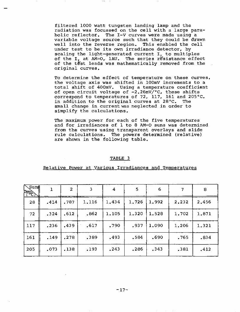
filtered 1000 watt tungsten landing lamp and theradiation was focussed on the cell with a large parabolic reflector. The I-V curves were made using avariable voltage source such that they could be drawnwell into the reverse region. This enabled the cellunder test to be its own irradiance detector, byscaling the light-generated current I L to multiplesof the I L at AM=O, lAUe The series resistance effectof the test leads was mathematically removed from theoriginal curves.
To determine the effect of temperature on these curves,the voltage axis was shifted in 100mV increments to atotal shift of 400mV. Using a temperature coefficientof open circuit voltage of -2.26mV/oC, these shiftscorrespond to temperatures of 72, 117, 161 and 205°C.in addition to the original curves at 28°C. Thesmall change in current was neglected in order tosimplify the calculations.
The maximum power for each of the five temperaturesand for irradiances of 1 to 8 AM=O suns was determinedfrom the curves using transparent overlays and sliderule calculations. The powers determined (relative)are shown in the following table.
TABLE 3
Relative Power at Various Irradiances and Temperatures
~ 1 2 3 4 5 6 7 8
28 .414 .787 1.116 1.434 1.726 1.992 2.232 2.456
72 .324 .612 .862 1.105 1.320 1.528 1.702 1.871
117 .236 .439 .617 .790 .937 1.090 1.206 1.321
161 .149 .278 .389 .493 .584 .690 .765 .834
205 .073 .138 .193 .243 .286 .343 .381 .412
-17-

The values in the table were plotted as the ordinatewith the irradiance as the abcissa and the temperatureas the parameter. The plots are not linear, so a"range of interest" was devised such that the expectedtemperature and irradiance levels would be included.Within this IIrange of interest", straight line approximations can be made. The graph is shown in Figure 2.Five equations were derived, one for each temperature.They are
28°C - P = .3318 + .123
72°C - P = .2458 + .123
117°C P = .1698 + .099
161°C P = .1018 + .086
205°C - P = .048 + .092
where P is the relative power and 8 is the irradiancein solar constants.
A graph was made, plotting the coefficient of 8 and theordinate intercept against the temperature T as shownin Figure 3. A second-order polynomial was fit to thecoefficients of 8 using the values at T=28, 117 and250°C. This polynomial is (2 x lO-6T2 - 2.11 x 10⁻³T +.389). For the ordinate intercept a least squaresstraight line was fitted, taking the form (-2.23 x 10⁻⁴T+ .13). The factor 143 was added to convert therelative value at 28°C, AM=O (0.414) to 59mW. Thecomplete equation is
P=143 [8 (2xlO-6T2-2 .11xlO-3T+. 389) + .13-2. 24XlO-4T] (2)
P = power in mW from a 2 x 2cm cell
S = solar constants
T = cell temperature (OC)
The equation fits the measured data rather well. Thesolid triangles in Figure 2 show solutions to theequation for various values of T and 8.
A program incorporating the two equations was writtenin the BA8IC language for the General Electric MKIItime-sharing computer. A fraction (X) of the cell areawas assumed covered by a reflecting grid with a solarabsorptance of 0.1. The solar absorptance of the cellactive area was assumed to be 0.85. Previous trialsindicated that the optimum value of X lay between 0.55and 0.70, so X was varied between these limits in 0.01increments. It was assumed that the final power was
-18-

II
-j !,
,,
,!
,i
28
C7
2C
l.~i
tmit
mH§E
H§EH
m~mm
ffff
fi!-
Hm.r
imtf
mtfm
tfmt
fm!m
#m#'~,~m'
~'!m
!fff
i'++-H--H-++-~_1
/1++
--+-+
+-+-
++--+
-++-
+-++
-+-+
+-++
+-+-
++--+
---'--
;-+-+
-+-+
++-,-
+j-+
-+-+
+H,
,-j
-i-
./--
r,J
.I
rJ,
r-T-I
I,
tt'T",'*
,"","'f
-h-+
-+T
/--',~,-
+-+
-H-+
-+-+
-1I-
t-+
+-H
-+-+
H-i
,'
1.
2H
4+
++
- H-+
+f-
H-+
+-I
-HH
-il.
"'
,I
'.+
_~I'-+-
_-!
-lL
".-L
±::
',:
I'
II
:~
:-
J~!,:
;/J
LL
L~-
L'"
'1::
!:
1.++
-+-"
-'_
'~"
rr:..-i:
.-""'+-
'......
.-1
,-.+-
+!-+
1-'-H-+-+-'~+-;-,-i..~-
--:-,-
i,-I
1-++
++-+
++++
-+++
+-++
-++-
-L-
+-+-
II
"lk
'11
-I_
LL
-+'I
I,
I,
-+-j,
I'i
.~.
+:,'
",
P(
TKfL
:1..
-t-<
--ZA
-,!,
....
~,.,
~A,
II-+H-++t--iH+-I-f-'-++-H-+--t~I.I!--+-+-
_L
..
L~..
,'~r-4~
H--
.-;-
--+
,,
'I'
','~"
,"
Lf-"
[I.
'!
"""
''.
\I
11
j'
II
I!
II
II
i..A
",
II
IIIi.
,'
ii
I,
,_~
Lit
H.l-
::jSk
'i.I
-l._
~_i~
:(,
iI._
!-.i
·f_L
~_-
-f-L-
f.-f+~-~,
1'"
.-+
-;,
f-+,:-
'--'-,
':..L-L~!
iI
I-l-
l..L
+-H
K-l'fl+!-~j-\+I~:
,II
fIA
_~
J-L
L.!
-'-I
TT
-I_
II'.~_L_+--.
-rlL
.I/
)1
1I
IfT
Trr,
Ij
I'.
I1
',.;
f.
I
I-+-+
-+-+
-+-+
++-+
+-+-
T-+-
+-t--
t-i---
ift--t
-f-I
I'~.i'
LL
U~c
'i.J
'Litf
'f..."
I,
,,
IH+H
·-++-
t":t-t
·Ij
,,
,....L
.L.:..
..H
++
-H+
-H-+
+J-
C:+
+-I
-t--
+-'
p\'-
I:-I
I\~j
'1
'~T
L..L
.L_~~
l,-
-!
L,l-:
L,r'-t~,
W-i
II
...!."
!,+L
-i.
,_,...
+-,
I-f-i-
-+-+
+++-
H-f-
+++-
i-Hf--
,Y-+
-+-,+
+,I
jI
--r-
II
II
I;
!I
•;
i!
II
II
Ii
I:'
,TT
Ii.:
-r-I
j
c:;
W ~0
.80 0.. W
I>
~.....
.f-
;(,
0~
I...:
lO
.W 0:
:
I,
Ii
II!
IH
I,
;.'1
'-:-+
+OU.
.J.I.J
.i"':"
.L';'!
...LI_
i-+-W;
..l.l.
..J:U:
..L..L
.L.LL!
..JLl.
.l..L.
LLLW..
J.~.J.
..L..L
LLi"":
'...L.
.L:!-L
L.J...
.l...L
.J...l
..Ll..
.!~-I.
"':'.J
...J..
.l-Wu~
.,j..J
..""".
l-W...
.l"';'
.J..t-
........~_
h-"-':-I
.I-_-~f-
_t,-,,:+
':ll::t~
ci:.t:t~
ci'::.
..:_-,;.:-
+-,_·:...I
r_':-_._-:
-.......;:
~_-,;.:-'-
-+-+-;,;.:
_;_:...
12
34
56
78
SU
NS
FIG
UR
E2
.R
EL
AT
IVE
PO
WE
Rv
s.
IRR
AD
IAN
GE
an
dT
EM
PE
RA
TU
RE

H-+--++-H-+-+-+--J ++--f--+-j-+-f--t-+-+-+--H--+--+-+-+-f-HH-+-f-I
-H--+1'\,,/-,-H+--+-:-I-i1*~ + Jt_LtM-!-- -,~+- - - U++--f--+-j-+-++-+-+-H- N- -i-++ -- -- -- -l I --q::
. 0 51-++-H-+--I--H_+-~ -1-+-1--+-1_- _ =:j::+_L-H__ '_+_++_J::++__H,,+-- _ ~_ :: _I _ rit:~t-:t->-'~=-- _- _ ___ j_-=t= .02
1-++-++-11--++-++-4--+-+--+--+--1--'---1.+-- - _+ __+-l ...+--I-I-1--+-1--+-+--1-- -r=Fl---- ---- -.- . --=- ==-=-l-r-
--I-t++-J-t-t--t-=-=--- ~ =-= ~ ~::__ -~ili - ::-:: -- -- ~ ---t ~.= =- -. -: == -- ==- -. ~~- -= == <,tJ ;H-+-H-H-+-I- , .- - "-t- - -- - -- -- - -- f1= - ------ - I! :
00 50 10 O~L...I.-J....l...J...-":1.l;:-5::-0-J...,l....l...J...~~2~O-=-O~..:...J....1......L.-L-!:2~5~OJ...LL..L.J.-Ll....LLLLl...LL.LLl-l..J 0
TEMPERATURE (OC)-20-

4.14
directly proportional to the fraction of the exposedarea. The results of these calculations are shownin Table 4.
TABLE 4
Output Power vs Fraction of Cell Covered
Fraction Temp. PowerCovered (X) (OC) (mW)
.55 168.2 44.26
.56 166.3 44.44
.57 164.3 44.59
.58 162.4 44.70
.59 160.4 44.78
.60 158.4 44.82
.61 156.3 44.83
.62 154.3 44.81
.63 152.2 44.75
.64 150.0 44.65
.65 147.9 44.51
.66 145.7 44.33
.67 143.5 44.11
.68 141.2 43.84
.69 138.9 43.54
.70 136.5 43.19
By inspection of the table, it can be seen that theoptimum reflective area is 0.61, with a resultingequilibrium temperature of 156.3° and a power of 44.83mW.It can also be seen that for the power to be within 1%of optimum, the reflective area fraction can varybetween .56 and .66. When the same analysis was appliedfor D = .72 (Venus), it showed an optimum reflectingarea of 0, indicating temperature control by this meansis not needed at Venus.
Series Resistance
For operation at high levels of irradiance such as aMercury or Venus mission, the most important loss factoris the series resistance. Consequently, for thesemissions the series resistance must be minimized. Assuming that contact resistances are not improveable beyondthe currently used titanium-silver system, the twoelements of importance are the diffused layer-gridstructure resistance and the bulk resistance. Sincesome 61% of the top surface of a Mercury cell must bereflective, a contact pattern can be derived using thereflecting area to minimize the series resistance.
-21-

_As a starting point, Equationmodified:
83 + 2W2
(-T-
(3 ) (Reference 2) was
= 0 (3 )
where 8 = grid separation
W = cell width (1.9cm)
T = grid line thickness
Pt = sheet resistance of grid line
P = sheet resistance of diffused layers
V = cell voltage at operating temperature (190mV)
jmp = cell current density at operating point(.26 A/cm2 )
The relationship T = 1.228/(.78-8), which was derivedfrom the area constraint was used. The resultingequation, a third order polynomial, was solved for acombination of diffused-surface sheet resistances andgrid-line sheet resistances using a ROOTER program inthe GE time-sharing library. The results, shown inthe table below, indicate a 3 or 4 grid cell would beoptimum if Equation (3) applies.
TABLE 5
Optimum Grid Numbers for Mercury Cells for Various
Cell Parameters
Pt Q/O P Q/O 8 (cm) T (cm) Ns
.005 40 .17 .38 3.3
.005 30 .20 .47 2.7
.005 25 .22 .54 2.3
.005 20 .25 .65 1.9
.002 40 .17 .39 3.2
.002 30 .20 .48 2.6
.002 25 .22 .55 2.3
.002 20 .25 .66 1.9
-22-
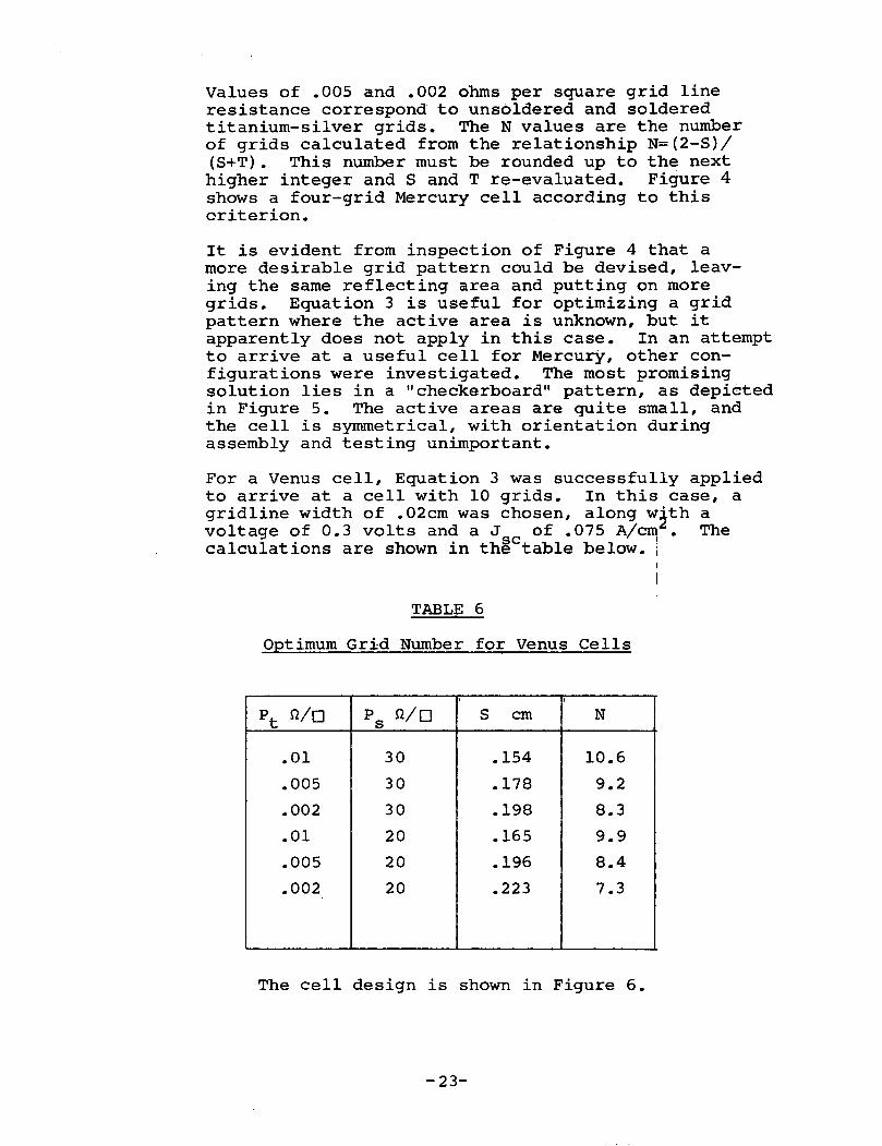
Values of .005 and .002 ohms per square grid lineresistance correspond to unsoldered and solderedtitanium-silver grids. The N values are the numberof grids calculated from the relationship N=(2-S)/(S+T). This number must be rounded up to the nexthigher integer and Sand T re-evaluated. Figure 4shows a four-grid Mercury cell according to thiscriterion.
It is evident from inspection of Figure 4 that amore desirable grid pattern could be devised, leaving the same reflecting area and putting on moregrids. Equation 3 is useful for optimizing a gridpattern where the active area is unknown, but itapparently does not apply in this case. In an attemptto arrive at a useful cell for Mercury, other configurations were investigated. The most promisingsolution lies in a "checkerboard" pattern, as depictedin Figure 5. The active areas are quite small, andthe cell is symmetrical, with orientation duringassembly and testing unimportant.
For a Venus cell, Equation 3 was successfully appliedto arrive at a cell with 10 grids. In this case, agridline width of .02cm was chosen, along w~th avoltage of 0.3 volts and a J of .075 A/C~. Thecalculations are shown in thiCtable below. i
I
ITABLE 6
Optimum Grid Number for Venus Cells
, I
Pt n/O P n/o S cm Ns
.01 30 .154 10.6
.005 30 .178 9.2
.002 30 .198 8.3
.01 20 .165 9.9
.005 20 .196 8.4
.002 20 .223 7.3
The cell design is shown in Figure 6.
-23-

Metal Contact
Active Area
FIGURE 4
FOUR-GRID MERCURY CELL
-24-

rt'looooff
o0't-
o
Metal Contact ,Active Area
r-------~----'--- -----.---- -
~~~~:;/ ~~~
~~~WJ~~~~
~~~~~~~~
~~~~~~~~
~~~~~~~~
~~~~~~~~
~~~~~~~~
~~~~~~~~
0.790 :f: 0.003
EACH ACTIVE AREA a .060 x O. 060SPACING 0.035
FIGURE 5
CHECKERBOARD CONTACT MERCURY CELL
-25-

FIGURE 6
GRID PATTERN FOR VENUS CELL
-26-

4.1.5
The optical and electrical characteristics of thediffused layer are not sufficiently understood toallow a mathematical optimization. As the sheetresistance is decreased from 33 ohms per square (theempirically determined value for lAU), the seriesresistance and the light-generated current bothdecrease. The change in series resistance is calculable and has been included in the grid optimizationstudies. The loss in current is not calculable andmust be determined by experiment. Starting values of20 ohms per square for Mercury and 25 ohms per squarefor Venus were selected based on earlier measurementsof the loss of current. These values representedgood tradeoff between I loss and series resistancescdecrease.
The base resistivity is in part responsible for theseries resistance of a cell, contributing about .05ohms for a 2 x 2 cell with 10 ohm-cm base resistivityand about .01 ohms for a similar cell with 2 ohm-cmbase resistivity. At a current level of 300mA (fora Venus cell) each .01 ohm of base resistance createsa voltage drop of 3mV equivalent to 1% in power. Ata current of 400mA (for a Mercury cell with 61%reflective), each .01 ohm of base resistance createsa voltage drop of 4mV, equivalent to 2.1% in power.Hence, a low base resistivity is desirable. Theoryindicates that lowering the base resistivity to 0.1ohm-cm or even lower should produce good cells, withthe important advantage of high open-circuit voltage.In practice, the expected voltage increase has notmaterialized. A few experimental cells near 0.5ohm-cm have proven good, but these have been the exception, and even at these resistivities the expectedincrease in V was not observed. Based upon presentstate-of-the-~~t, base resistivities in the range 0.8 1.5 ohm-cm are suitable for both Mercury and Venuscells, because the bulk silicon contribution to theseries resistance can be reduced adequately withoutseverely decreasing I sc •
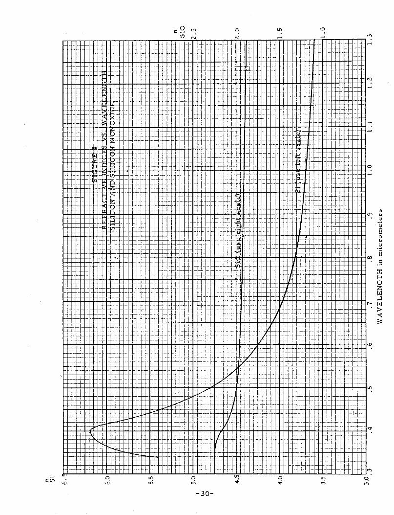
Effect of Shifting Reflection Minimum to Longer Wavelengths
It was mentioned earlier that a bandpass filter offeredtheoretical advantages for reducing the input energy toa Mercury cell. An hypothesis was formulated whereinthe reflection minimum of the SiO anti-reflectioncoating normally applied to solar cells would be shiftedto longer wave~ergths where the efficiency of solar cellsis higher·~nd would lower the temperature by reflecting some of the· less useful short-wavelength solarradiation with a net increa~e in power. The currentlyused SiO thickness is 8xlO- m (800 A) corresponding toa reflection minimum of approximately 6xlO- 7m (6000 ~).
-27-

Calculations were made to determine solar absorptanceand power loss due to decr~~sed.film_~ran~miisionforofilm thickness from 7xlO-~ to 12xlO m (70QA to 1200A).
The variation in solar absorptance with film thicknesswas calculated using equations giving reflectance asa function of component indices of refraction andthickness, applied at 20 selected ordinates (Ref. 4).The reflectance equations (Ref. 5) are
2 2 2rl 216r l + r 2 + r2 cos
R = 2 2 (4)1 + r l r 2 + 2rl r 2 216cos
where r l = (n - nl)/(no + nl
)0
r 2 = (nl - n 2 )/(nl + n 2 )
R = reflectance of assembly
no = index of refraction of air
n l = index of refraction of SiO
n 2 = index of refraction of Si
rp = 2 lT n l e/~
e = thickness of SiO
?-... = wavelength
Assuming that the assembly does not transmit anyradiation, the absorptance is given by A=l-R. Thecomputer was used to solve Equation 4 for the 20selected ordinates using index of refraction valuesshown in Figure 7 (Refs. 6-8) and for film thick-
o 0 •nesses from 700A to 1200A. As shown 1n Table 7, thetemperature (calculated using Equation 1) does indeeddrop with increasing film thickness, and the relativepower due to this temperature drop (calculated usingEquation 2) does increase.
-28-

TA
BL
E7
Tem
pera
ture
an
dR
ela
tiv
eP
ow
erfo
rV
ari
ou
sS
iOT
hic
kn
ess
es
Sio
~F
or
So
lar
Eq
uil
ibri
um
Rela
tiv
eP
ow
erL
oss
Ov
era
llT
hic
kn
ess
Rm
inA
bso
rpta
nce
Tem
pera
ture
Po
wer
Due
toC
oati
ng
Po
wer
(nm
)(n
m)
(s)
(°C
)
705
32
.83
91
51
.2.9
88
.99
2.9
80
80
60
8.8
34
15
0.2
11
1
906
84
.82
61
49
.81
.00
5.9
89
.99
4
10
07
60
.82
21
49
.41
.00
9.9
66
.97
5
11
08
36
.82
01
49
.11
.01
3.9
37
.94
9
12
09
12
.81
31
48
.41
.02
1.9
08
.92
7
-29
-
n Si hH
-+++
+-+-
H-l
-+++
-+-H
-+++
+-+-
H-+
-+++
+-H
H,-+
i++-
1-+ '-
+'+--
'-+-H
H-+
++
++
-HH
-++ '-
!'-+-
++++
HH
-+++
++H
H-+
+++-
HH
-+-+
++-'-
-'-H
.....l
.-+...
l-++-
HH
-+++
-'j-+
,--'--
lH
H-+
++
+-f
-H-+
++
++
-H-+
++
+-+
-H-+
-++
+.+
-HH
-+-1P-
H-+
-+++
+-+-
:-,H
-+++
+-+-
H-+
-+++
+-+-
H--
+-+'
-IH,-+
,-++-
i'-+!,.
.'++;-H--+~++·~-HH-+I-+,
+-,-+
'-+:-t-+++-H-+-++~+-l
H--
++
+H
H-+,
-bJ.*
:-IH
-+-+
+-H
-+-+
+-H
-i-++
+-H
-+-+
--i--T
-i-i
++-H
-+'-"
Y-+
-L..L
-H-+
-+-+
-HI-+
+++-
H-+
-+-+
,-++-
+-+:
-1-+
-+-t,
-::--+
+n-i,-
+,+~-+'-
.+.6'.'.
-:.-.
r:...,'-
-++-
:'-+'++
+-+-
-1-,-
+..;.1
-+:"":
--7+--
'-t-",
t--,H.
-+++-,
-i-':J
f~'!-+
-·~.'+
+-H
H-+
+++-
+-H
--+-
-;--;'
..!.
j!iii
1+
+-t
-t-H
-+-+
+'-:
'--+-
+....L
++-r-
h-,'!.~
,_.~11..1..
a_
i-H
H-'-
+'-i
i--+
--r-
+-'-
""-+
-'-'
-+++
.-~"
rlI
;!
•I
I!l-r
-I
II'
IJ
'tI
jIi.
.--I,
II
':
II
II:
HH
-++
+''I
,''j-
i-t
'1'I
1,'
H--
i,T
TT
TI.
,,
f<.f<
HA
Q,V
II"·I<
....I
VS'
.W
:AV
.H
6.0
HH
-+++
-Jf.+
'+-t-
+-i-;
,,--+
I-+++
+-H
H-+
+---1
,--+,-+
+:-;
,,
""
",;
I';'
.:Ul
~!~r'I
_~,--'
?-~~#~
~!.!f!
+'MU-!l'i
l..i",.J1
'ir4--¥"£X~
:.'r'J~:~
t"''i-';'_-.
,.;'''_1-.J-
'-_--Jt-_-.;
..'-_1---!+_
-+-I-_1f-_l-
~~_-.J'''_~~
~'-l-lHH-++-hfi--I-H-t+-1~H-++++-HH-++++-HH.....l.-++-;-·7-+--:,H-++++-HH-+-+++-+-HH-+--j--r+-+-n'4"T'r-
II
II
Iiii
!
HH
-++
+-'
-'+
'++
+-j
-'-!'
-+f
\++++--I-H-+--,..++-+-H--+~+--'-t--I-'
..,!
H-'
-+--
'-+
-+-H
-+_L
I--H
-++
++
-+-H
rl-+
-+-+
+-+
-H--
+_+
++
+1 _+1 ++
-+-H
-+-+
-i-' -
:1-+
'_+-/-
+,'·:.
.·.;....
·r:+--'--'-H-t+....L-t--'-t--r--,-+~-l
!I
1I
i
,,
,I
,i_~
II
I\1
I!
I-;
'_+
++
+1+
,++-
+_H
-+--
++-',
-+-,-
-'-,..,
....+
--i-_
'-.;:
--!
:i;
Ii.
l_~~.
'1
II
Ii
j
I-"H
-+-"
',:,.f+
-..;--
!-H
--I-
++-i\
.-'-H
-t-++
+-+-
H,'-
-,I-+
---'-
--.-.
,-;f-
!---
i---+
-:-+-
'--r-
·;-:
~.'~,
;---1- 1
+t+-+
I-!-
-++-
:'I~++
-f-+-
t.-t,-
~,'~
-_:-+
--'-
;-;.~~
'.~+-
'--;
-r-+
-,--
-:--
--I-
-II-
-H-+
,-'H~-,-+....L+-+-HI~,--++++-+--H-++-:-+-+-
......-
--'-
t--H
..--
-'--
-r--
r--i
Ti-
II
t-+-+-
~i
If:
I
5.5
II,
(.\-
_:-
+t-+
-!.-L
h-+
--H'~
.:,
II
++;..
.1+-+-+--+----+~_,_-'--r-t-C...JI-+'-;..++.l-~,.-j
H-+-+~-+-ilH-,
++
-H+
-HH
-+-+
+-l
H-d
=±
I+H
-r-
f;-~-'-
---'_.,
..1+._-+
I++H
-+'+
+-r
l-+
+-H
1-+- 1+-H-+-+--+-H--;--+-t-1-+.,+-Y~-+-H-t+-H-++-'-H-+M--'-+-t--"-+-'-t
-H-r
-'-H
f-cH
-+++
+-+-
H-t+
++-+
-f\-j
--+_
+'-'H~
!,
ii
.I~:
J.-1
jI
I:
I!
IiIi:
!\
I:
I,
iT
;:
II
II!
II
i
, W o I
------
-.-;.-
,, 1
.3
,1
i,
1
11
!1
,I
:;-r
-lil
T.9
1.0
11
1.2
.8.7
WA
VE
LE
NG
TH
in.m
icro
mete
rs
H-+
-+,-,i
-,I--
i---
-r-I
--'-t
--'
II
I~-l--4-
-+~c-'
-'-+
-+--
-'--
-jIH
,_·~
++-,
I-+:
+1++
-+-i-
--i--
+-+-
.H,-+
++++
-HH
-++-
+-+-
+-H
-+-+
++-'-
t-H-+
-+-+
-+-'-
t-H--
+--r
-+++
-HH
-+++
++....
.HH-
-'-....,
..-+-l
H--
++
-J-'
i---
'-ji-
t-'+
-t--
Hil -+
-It-1
i±tf±
!ir-:±
J+-!-
,,I
+++:+
-H--+
-++-
H-+
+-H
H-+
+-H
t++-
+--+
-+++
-+--+
-+-+
+-C
H--e
+-+-
-i-i-+
+-+-
-+-H
-++-
+--i-
-t-1-
+-.,.
-+--
-;-+-
-,-,+
h1-
I-H
-Rtf+
:-1_
L,-
L.-i
-.L.+-
;-H-+
+-+-
-t+-H
-+--t
++-+
--+-1
-++-
+-+-
H+-
CH
-H--+
-i-+-
H--'
-H--l
-t--+
--t++
-+-+
--+++
-!-+-
+-+-
Hf-
3.0
.3.4
.5.6
4.1.6
However, there is a loss in light-generated currentdue to the increased reflection of light in the wavelength range where the sunlight is most intense. Thisis demonstrated by the reflectance curves shown inFigure 8. To determine the magnitude of this loss, ashort computer program was written wherein the spectralresponse of a bare (uncoated) cell was multiplied byboth Johnson's curve and the ratio of (l-R) of thecoated cell to (l-R) of bare silicon. The resultswere summed across the spectral range of the cell.Mathematically, this is given by
I -_ r l-Rl,L, __---l..L(A,;.t.)__J(~) * R(},\ * l-R
2f~ (A) (5)
where I = current
J(I\.) = solar spectral irradiance (Johnson)
R(A) = relative response of uncoated cell
Rl (f\) = reflectance of uncoated ce 11
R2 (>J = reflectance of coated cell
These results are also shown in Table 7, wherein therelative power is equated to I in Equation 5. Whenthe two relative powers are multiplied, it is apparentthat no net gain is achieved by altering the antireflective coating.
Cell Designs
This section describes the cells designed for Mercuryand Venus applications. All aspects of their designhave been considered. A summary of the parametersused was given in Table 1.
Base Resistivity and Type:
a. Mercury - 0.8 to 1.5 ohm-em, boron doped
b. Venus - 0.8 to 1.5 ohm-cm, boron doped
Junction Characteristics:
Mercury - 20 ohms/sqa.
b. Venus - 25 ohms/sq
-31-
-5(""-6 x 10 m) phosphorus
-5(~5xlO m) phosphorus

~I·t±j
!i;
,-:<~
_._.
1-1~
-r'.
:j-L
TI:
:'.
-.
--
_
I_
•.j.
_--
_..~
.:...--~-:-:-~~~~-+-
-+-t
-L!
.._~.L
· t·.1.-
-~
......~-
-.
----
-..,-,----:'
.-f-
----
!-.-
-,-
--.-
-;--
---.
•-..~
_•..
..._
..,-
4_
--:-
_....;._
_._._~_,
.._.~__
.__
._.
_...
....
._."
.;
-.
:.,..;
"._.
_._~._,
.:__
._•.
_0
_::
.
---
---
----
..---
--.-
.--.
--_
.---
--..-
1--
,'
-,
-I
'
--
•0
-•••.
_••••
_:.-....:
_~_._
_....
:.
._.~.
--..
.-
f---
---
-.-
1----
----.-
_.•
----
.--
---
---
,-
__
_.0
..
0._
_._
._
I'
.5i-!..I/I~
_,
'',
_'
-Lt,
_,I
.,V
:",
!!:-"f\
'-"
---
-!:~;.~/
::::
1\:-'
,:~
:-
-.-
..-::-
~-~:---'
...:=
::-~-:~-=--.:~-:
AN
TI
tEE
tE
CT
1p
N...G
cA
tfN
:;C
Hi
Et.
Aci
tiiS
::re
s•
.•
._
._
._
..
-0
._.-
__
''1~
,I .;-.
_,-
,I
!:_J
L
i:·!i\f:~~
I4-H
--!-:;
:X:'
-~:
'!.-
~.;:
"-.
/\
\----
--r--,.
--'
.-:'
-:-,
;-
...I~~~
-\,\
I W '"I
-,~--
~;.J-.~~
-,:
,---
-_.~
1.2

Contact Material:
a. Mercury - sintered titanium-silver, solderless
b. Venus - sintered titanium-silver, solderoptional
Grid Pattern and Size:
a. Mercury - See Figure 5
b. Venus - see Figure 6
Anti-reflective Coatings:
-8 0
a. Mercury - 8xlO m (800A) SiO
-8 0
b. Venus 8xlO m (800A) SiO
Handling Characteristics and Restraints:
a. Mercury - no restraints. Since cell is symmetri-cal, it can be used with any edge asthe contact.
b. Venus - no restraints. Handle like conventional cells.
Production Cost and Implementation Time:
a. Mercury - the cost of the Mercury cell will beslightly greater than conventionalcells because one additonal evaporationis required. The implementation timewill be the same as for other cells,being limited only by acquisition timeof evaporation fixtures.
b. Venus - the cost of the Venus cell will besimilar to conventional cells. Theimplementation time will be the sameas for other cells, being limited onlyby acquisition time of evaporationfixtures.
Weight:
a. Mercury - same as conventional cell (2x2crnx.036cmthick), 0.35 gram.
b. Venus - same as conventional cell (2x2cmx.036cmthick), 0.35 gram; with optional solder,0.41 gram.
-33-

Special Tooling:
a. Mercury - special evaporation mask required,8 fingers, each 1.5mrn (O.060 in.)wide.
b. Venus - special evaporation mask, similarto conventional but for 10 grids.
-34-

4.2 Outer Missions
The target missions for orbits outside earth orbit areMars, the Asteroid belts and Jupiter. Table 2 aboveshows the progressively lower values of solar flux andtemperature expected on these three missions.
4.2.1 Optimum Grid Numbers
The predominant cell losses change from series resistance losses which were dominant for the Mercury andVenus missions. However, there are still slight gainsto be made by varying the grid line coverage, and forthis, the analysis given in Section 4.14 is appliedagain, using equation (3) to compute the actual numberof grid lines to be used for the outer missions. Thecomputer solutions for the optimum grid patterns forthe three missions are given in Tables 8 through 10.The sYmbols used were defined in equation (3), inSection 3.4 above.
TABLE 8
Optimum Grid Numbers for Mars Cells
for Various Cell Parameters
PTPs S T N
Ohms/O Ohms/O cm cm
.005 30 .418 .02 3.61
.005 35 .398 .02 3.83
.005 40 .382 .02 4.07
.002 30 .430 .02 3.53
.002 35 .409 .02 3.76
.002 40 .391 .02 3.96
-35-

TABLE 9
Optimum Grid Numbers for Asteroid Belt Cells
for Various Cell Parameters
PT Ps S T N
Ohrns/O Ohrns/O ern ern
.005 25 .715 .02 1.75
.005 30 .675 .02 1.91
.005 35 .642 .02 2.05
.005 40 .616 .02 2.18
.002 25 .729 .02 1.70
.002 30 .687 .02 1.86
.002 35 .653 .02 2.00
.002 40 .625 .02 2.05
TABLE 10
Optimum Grid Numbers for Jupiter Cells
for Various Cell Parameters
PT Ps S T N
Ohrns/O Ohrns/O ern ern
.005 25 1.149 .02 .73
.005 30 1.084 .02 .83
.005 35 1.031 .02 .92
.005 40 .987 .02 1.01
.002 25 1.164 .02 .71
.002 30 1.096 .02 .81
.002 35 1.041 .02 .90
.002 40 .996 .02 .99
-36-

From these tables it can be seen that four grids arerequired for the Mars mission, two for the AsteroidBelts and one for Jupiter. The various values used forgrid line and diffused layer sheet resistances are alsolisted along with the solutions of the equation forgrid separation (S).
The next sections discuss the various loss mechanismsexpected at the outer mission operating conditions.
4.2.2 Effects of Decreasing Intensity
As mentioned above, the decreased intensities generatecorrespondingly lower current densities. The shortcircuit current decreases linearly with intensity ifthe cell is maintained at near-earth temperature(~30°C). This can be seen in Table 11 which lists theaverage values of I for 70 Nip cells (of nea5-Earthconventional designfCmea~ured at AMO, l40mW/cm (nearEarth) and AMO, 5.2mW/cm (near Jupiter) conditions.
TABLE 11
Effects of Decreasing Intensity for Cells at 28°C
2Intensitv (AMO Spectrum) mW/cm 140 5.2
I (4cm2 Nip cell) (rnA) 142 5.5
·scaverage
1V0c(4cm
2Nip cell) (mV) 555 455average
K::FF = p II V .73 .705max. sc' oc
Conversion Efficiency % 10.3 8.5
The open circuit voltage V also decreases with decreasing intensity when the cel~Ctemperature is held at 30°C.Table 11 compares the V values at the two intensities,also the values of curvgcfill factor (CFF=max. powerlIx V ). Thus, considering intensity decreases only, scthe080nversion efficiency of the cells would decreaseslightly for cells held at near-Earth temperature, andmeasured at the lower intensities, as seen in the table.
The decreased V is not predictable from the I decreaseonly, probably Bgcause of detailed differences ~g PNdiode behavior at different light intensities. This meansthat at present actual measurements must be made forcomparison.
-37-

Fermi level separation, andsaturation current; therepredict the V changes
oc /for d V are around -2mV °C.ocdT
4.2.3.1
Effects of Decreasing Temperature
The effects of the lower temperatures expected forthese missions have a greater effect on the cellproperties, and they provide the major problems whichhave to be overcome in order to optimize cell output.•
Not all the effects of low temperature operation areharmful. Most important, the open circuit voltage(V ) increases with decreasing temperature, and thera€~ of increase of V exceeds the rate of decreaseocof other parameters such as I and CFF.sc
Therefore, with good design, the conversion efficiencyof the cell for operation on the outer missions canincrease significantly and steadily, reaching the 1618% range at Jupiter distances.
Effects of Temperature on Voc
As mentioned above, V increases as the temperaturedecreases. The main Bhysical reason is the same asthat causing lower V for the higher temperaturemissions, namely, th2Cchange in the forbidden energygap width (Eg) with t~mperature. The quoted valuesof dEg are -2.4 x 10- eV/oC. (4) The Eg change can
dTeffect V by altering thealso by 8hanging the diodefore it is not possible tofrom dEg. Measured values
dT
There is some variation in measured values of d Voc '
dTdepending on the value of illumination intensity usedto measure V , and also depending on the backgroundresistivity 8~ the cell. For conventional solar cells,the energy gap does not vary much over the impurity 14concentration range used ~o make good cells, (5 x 10to 1016 impurities per cm ) but the position of theFermi level approaches the band gap edge more closelyfor higher concentrations and thus allows greatervalues of V to be obtained when higher concentration(lower resi~€ivity) silicon is used as starting material.
Figure 9 shows approximate curves for V versus temperature for two illumination intensities aHa two resistivityvalues. Temperatures corresponding to missions ofinterest are noted. Other curves can be found inreferences 10 through 15.
-38-

These changes in V are basic and cannot be alteredby design. Howeve2? they provide one criterion fromwhich the optimum resistivity can be chosen. FromFigure 9 it can be seen that for all temperatures ofinterest here, lower resistivity silicon has a greaterVoc value although the differential decreases astemperature decreases.
4.2.3.2 Formation of Schottky Barrier
It is sometimes observed that V does not increasesteadily with decreasing temper~€ure, and this arisesfrom the formation of a Schottky barrier at thesilicon-metal interface at the back surface of thecell.
Schottky barriers are among the oldest potentialbarriers used in semiconductor work, and have widespread useful applications. In the past several years,great improvements have been made in controlling andmeasuring the properties of various metal semiconductor barriers. In the present work the Schottky barrierbecomes appreciable at lower temperatures, and underillumination, can provide a photovoltage opposed to themain piN junction, and thereby decreases the availableV of the cell. Although unusual, such Schottkyb~friers have even been observed at near-Earth temperatures as a result of cell processing.
For example, Nip cells with titanium-silver contactsdo not normally have appreciable Schottky barriers.However, after dip soldering, Schottky barriers givingphotovoltages above 30mV can form, leading to a "solderdegradation" in cell properties. In this case, themechanism of barrier formation is metallurgical andinvolves interaction of the solder components and theTi-Ag with the silicon surface. The remedy found foroperation around 30°C was either to alter the treatmentof the silicon surface before evaporating Ti-Ag or toprovide a highly doped layer at the back siliconsurface. Schottky barriers are lower generally as thedoping level in the semiconductor is increased, andtherefore the addition of a highly doped like-impurityis an effective means of minimizing barrier formationat all temperatures.
For low temperature operation it is therefore necessaryto ensure that the back silicon surface is highly dopedimmediately next to the lowest metal layer of the backcontact system. In practice, several ways of doping(diffusion, alloying or ion implantation) are available.For example, a separate diffusion procedure can beintroduced during cell fabrication to leave a thin,highly doped like-impurity on the exposed bulk of thecell. If this is done before the main piN junction
-39-
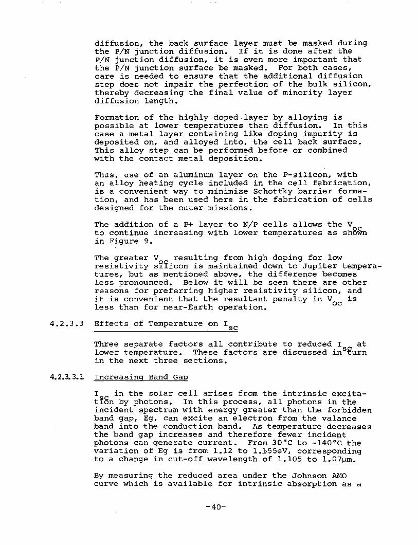
diffusion, the back surface layer must be masked duringthe piN junction diffusion. If it is done after thepiN junction diffusion, it is even more important thatthe piN junction surface be masked. For both cases,care is needed to ensure that the additional diffusionstep does not impair the perfection of the bulk silicon,thereby decreasing the final value of minority layerdiffusion length.
Formation of the highly doped layer by alloying ispossible at lower temperatures than diffusion. In thiscase a metal layer containing like doping impurity isdeposited on, and alloyed into, the cell back surface.This alloy step can be performed before or combinedwith the contact metal deposition.
Thus, use of an aluminum layer on the P-silicon, withan alloy heating cycle included in the cell fabrication,is a convenient way to minimize Schottky barrier formation, and has been used here in the fabrication of cellsdesigned for the outer missions.
The addition of a P+ layer to Nip cells allows the Vocto continue increasing with lower temperatures as shownin Figure 9.
The greater V resulting from high doping for lowresistivity s~Iicon is maintained down to Jupiter temperatures, but as mentioned above, the difference becomesless pronounced. Below it will be seen there are otherreasons for preferring higher resistivity silicon, andit is convenient that the resultant penalty in V isless than for near-Earth operation. oc
4.2.3.3 Effects of Temperature on I sc
Three separate factors all contribute to reduced I atlower temperature. These factors are discussed inS€urnin the next three sections.
4.2.3.3.1 Increasing Band Gap
I in the solar cell arises from the intrinsic excitat~gn by photons. In this process, all photons in theincident spectrum with energy greater than the forbiddenband gap, Eg, can excite an electron from the valanceband into the conduction band. As temperature decreasesthe band gap increases and therefore fewer incidentphotons can generate current. From 30°C to -140°C thevariation of Eg is from 1.12 to 1.155eV, correspondingto a change in cut-off wavelength of 1.105 to 1.07~m.
By measuring the reduced area under the Johnson AMOcurve which is available for intrinsic absorption as a
-40-

--rc1-+-W-+-U+-J--I-I-++-J-+I+++--1-N-N+t++1-+t++-I+t++t-r-tTil,-+-I--l..--+-;H,- t-
1000 fiil"H-++-H- 1- -~++++++--j-,+-+"'~-+-I-+-~-t-
W-+-.-+-+-I-+-+-.-+-+-I-++++I-+--H--j--H-+t-+-- 4-+-++I-+-H+H--H*t+ft~t-t-t4"t""t- t- -+-++-++
- 1---
I--+-l-+-+-I--++-+--f-I--+-f-++-il--+-+t+i- j--
~-++-t--~--I--f--+_·+t+H-+++-t-rH-"M-t+--.-+-l--l-I-+--I-J-+I-++t---1'H-+t-rH-i-t-+-H-lj--- -
~++++-++-
200
I-+-+-+-+-++--l-l-i- ~t--W--H-+-~W-+-l+J+++--HH-++-H+H-H+l+ttti~H-ttti-t-rttiilTtttjjjttjj
T -1-- -W-W+W--I-l--f-+-W~-Hr-+H-++++-1H-H--t-1H-t+++tt+t+t-HH-H-tttT+tTi-n-H
o []]rnII.lIllllLLLUUJ_~7,t0-U...Ll....LL_~2hOt-LLLJ...J....l...l_-=t7*0...L.L.LL..l...l....t.:_~2~0:-u~..J...I.~-3:tiOr..L...l.-.I.-J,...;~
Temperature (OC) -41-

result of this change of cut-off wavelength, a decreaseof 2.5% in I was estimated (see Figure 10). Thisloss will beS€he maximum expected because all thecarriers generated at these longer wavelengths will notbe collected at the junction.
4.2.3.3.2 Decreasing Absorption Coefficient
Current is generated as light is absorbed in the silicon.The absorption coefficient varies with wavelength, andthis variation is usually combined with the variationfor incident illumination with wavelength to computeIs. The abrgfption figures most used are those of Dashana Newman ( and they showed that at 77°K there wasless absorption than at 300 0 K (see Figure 11). Shumka (17)has analyzed the effects of this lower absorption on I scand calculated for temperat~res from 30°C down to -40°cthat d Jsc is about 12~A/cm 1°c. However, as mentioned
dTbelow, actual I losses are not always as high as calculated, indicati~~ again that the collection process forcarriers generated by the longer wavelengths has a largeeffect on I sc
4.2.3.3.3 Decreasing Diffusion Length
In addition to decreased generation of current by theeffects described in the last two sections, there isalso the possibility of reduced collection of the currentcarriers as the temperature decreases. This arisesfrom decrease in the minority carrier diffusion lengthat lower temperatures. This effect has not been emphasized much in analysis of cell behavior at low temperatures but measurements show it is an important one.
Measurement of minority carrier lifetime versis temperature shows a loss of )50% as the temperature decreasesfrom 300 0 K to 200 o K. Extrapolation of this loss toJupiter temperatures (130 0 K) shows that the loss couldapproach 70%. Even if the lifetime saturates at a lowvalue it may still only be 20% of the near-Earth temperature value.
L = J D'r where L, D, and T are respectively, the diffusion length, diffusion constant and lifetime forminority carrie~s. For the bulk region of the Nipcells, D = 39cm Isec. and does not change drasticallyat lower temperatures. Thus, L decreases from 225~m to130~m as T decreases from 14~s to 5~s, typical of valuesmeasured at near-Earth and Jupiter temperatures respectively. Use of the curve in Figure 12, which showsAMO values of I versus L, shows that I could decrease from 40mX7cm2 to 35mA/cm2 by the ~rme Jupitertemperatures are reached. This corresponds to I de-crease of 16%. sc
-42-

1.1A B
I-Hf-H-l··· f-- .++++-+-+-1 ;-·H-++-H-HH-t-+-++-i-i-.j.-+.w.+~-l-H-~-+++l+H--h-++~+t+t-t-H-ML.Ttt"t1
..... i'~-!C -
~r
1-++-+-++-+-+-+-H-++++-+-+-+-H-+++++'7! . ":(i~li',nh ·-h:r.. 1 iii I:...h~(rrh K
H-H-4-l-l-4-+-+-+-f-~-++-+-+++++++-+-j'E -lr-i~·~·'-ehi#4I~H--j".ti"h~-=jl1"h1tdti.-!h.:~;-lJ~ ~~ 4FI!J -)-!lfCiI -;'],-r:i' . I\. KI-I--W-++-+-t-+-H-++++-+-+-+-i-+++++-+-+-+-f-t-++++-+-+-+-f-t-+++t-H-t - -i- '. 'T I
fA
...+ '. ':·j:::·-·=-J='·i' .:- .~H+~-=-J=H=I..J'~ti--H_H-tl-,_+-· t-I-+-++-+--+·+-t+-if-t-H-l-++..L-l--1 ;_.H-H-l
f-++--l.-+--l--+...,H--+--t-++ l-I--J-+-t-i+~+++++-J+H-f-+-H+j+j+t++t-Hrt-t-++-+-H,
>;tJ1~Q)
t5 1. L~+-I-.+-+--+-+-l-I'-P.I-.i-~+-~-+--1H-W-.w.-W-l--iI+t--+..w.-H--Hf-+-t++-+++-Hf-+-H-+++-t+H--1++++-I+H-+-++t-t-i-j~(lj
....-lo
(J)
+Jffi o. cd-i-!-U+J.-H-i-I-t-+-l--+-l--H-4-P>k+-l-++-H+H-++++-H+H-++-H-H+H-t++t-H++++-+++-HH-+++t-t-H"0.r-!()
l=:H
o•4-l--l--+~+-I-++-1+-1+++1+1+t+-H-I-hH-l-H+++++++++++++++++-F~H-H-H-f-HH--i~~+t+H
o•21-+-1-+-1-+-1-+-1-+-H-H-H-H-H-H-H-H-1-t-f-+-11-t-1-t-1-t-1-t-1-t-1-t-1-t-H-H-1-t-H-H-H-H-H-H-H-H-t--h~17
olt±tti±ttttt±:ttt±tl±±±±±±±tijjj±ttjjjjjj:ttJttttttttttttttlttt±tl±tt±l:t~0.4 0.5 0.6 0~7 0.8 0.9 1.0
Wavelength (~m) -43-

L
l-
4
lQ-~II•••••I·"2
10
ouzw·L:I,;N ..... 0
~z0:wD .......
z~W I~ SW U
o ~ ,- 3..... w y
If) Ln Ul~ w
..J 2a: ua >q u(')
"'
DOW!l.<!l.
o7
-44-
t~jjjllllllt~[r~·JiJjj·llll1rrrlll~JJjll11Irrrl~r~~JJl1!~111ltt~~:JjJ1 ,l +-r-~ '·r-0.4 0.6 0~7 0.8 0'.9 1.0
Wave'le~gths (J,lm)

~o.
_:1"[...~GEN~H~
SE
MI
tD
C\R
ITH
MtC
~.:
=Y
C,_
;::S
,.(C'
GIV
ISIC
JN
SP
C::R
INC
H
,I-r-
"r.-H
H-+
++-i+
H+1
-t1-t1
+t++
iH+H
t+t--
H++
++++
++H
-1++
1tr
ft+
I,m
---.
;-I-
f-H
-t'-jl
--++
-t-+
t+t+
t-H!
~-++
li+tt
fti-
!-H
-+r+
t-H
H-t
->-Hil+
+tt
+1
+-1
-r+-
-+-+
-H-+
+H+I
+t+-
H-t
+H-1
+ttti
-++-
+-++
i+t+
t+'f+
i+ttH
+
70
60
,"m
-II
11:!:
111
'.
I;,
(,;'
I-~
--_.-
--.r·
..-l-t
',TT
f7!-J
~-L;-;-
-c--
--
","
I!'.'"
,'"I'
IIi
-r-+
-H-+
+I-+
+I++
++++
+-l-H
++C~"::"=:''::~'~
I,iii'
f1jT
mIii
",
i,,'
Hitt,+
+,tt
,++l m,i+
,t-·t-
t-+-+
-+-+
-+-+
-H-+
+++f
+t+t
1H::1
;;....
.
30
~:-
-r",
'I
,'
,,
',I"
"l
i,I
I.11
I,II!
'IIi
----n-r
-(It'
I.,I
I;~.'
~'ill
-+-+++++-H-+~I"FH+t+t++++t+!++t+t++-+-H+t++++++I+++t-
-P-
--'~-
i-H'
If-H:
II,
I'!
I!",.
I,;I
,+;
-r++
+++-
H-+
+-II
+t++
t+t+
t-t+
tH+t
H++
i-+++
+t+t
iilol
-i'I"
t''I+
t--t;;:'T-'--~
Itit
II
;I
11I
-
I
II
I
'I
,,
:i
,I
'I'
,'I
,:"
,,
,I
Ii'II
'I,
Ic4
~-l:'!
!+-+,
--r-,-
'--I--
!-++-I
-+-t-t
-t1+Ii
+++l++
H+ttiH
-+,-t,
-t,~'-
H-+++,
+-,Hil
ll-+tl
H-H,-'
1~H-H
+t-
+-+
-+-+
++
H·+
H-t
1H-I
+I+
1f+
+ '++i·H
+ H+ H
-H-t1
H'H'
H-'~
-ett.m
-,
~I
,',
'."
~,:L,I':,,!
~t+++,H++-,+
-,++.'+'
+,+1H
I":-1
,4+
,,+-,'-I-l-H:,~:,:,-,I,ttt+tt--1-r+--+-rH-!-+H+1+t+t+++HII-tI-t++++-++-H+I+HIJ~
,"Hi+'
-,'1-4 ,
-+,2
0t-~!--;--+-'---'-+-H++-t+-HI-t
+;-!'
;-;1'
!:,I
.,i::
T,'
Int
I'"
[i,
i
,',
-I-
--t-+
-+-+
++-I
-++I
++++
++++
t-'+-'t-
++ '++
-'H+-
"-r++
++-+
+-++
+l-H
++++
,!
ii
!!
'!I
II"
IiI
rf
1iII
II
IIi!!
I'
-45
-
..=F
'_+'
--+-
+-H'
--+-
"H-t
-+t+
++~H
++++
-4+H
-+
.'~+tit=f+
++-tI
-+-H
++++
+H-+
--t-t+
H++
t+H
++++
+++H1*
-+-+
-1-+
1-','-1-
+-t
-t+
++
1ri
+H
-H+
+tH
++
HH
-+-t
-ttT
tH-t
rttt
tffit
tftt
t'+'-~-I--r"
'··......t
-+·H
-+H
-++
f+I-
t+i+
t+I "H
,t
i'tt
t+H
1+
ttt+
tHtt
tttt
ltl~'-'--_c
'1
09
0
(~m)
,1t-~
;+':
DIF
FU
SIO
NL
EN
GT
H,
La

S.chottkvbarr~er.
4.2.3.4
It is not easy to estimate the extent of the decreaseof I with temperature for a particular cell. Theover~Il decrease can often be less than those estimatedhere because the measured I losses from 20°C to -130°Cfor both 5mW/cm2 and l40mW/~~2 can be as low as 8.5%.However, the spread in I losses was from 8.5% to l~/o
at Jupiter conditions, sH8wing that the relative importance of these I losses may vary. All three decreases in I are ~8st pronounced for longer wavelengths. Th~~ can be seen in the measured changes inspectral response (18). Analysis of long wavelengthresponse of cells as a function of temperature mayhelp to isolate the effects of the various I sc lossfactors.
Effects on Curve Fill Factor
One of the factors affecting CFF is the diode saturationcurrent (I ), CFF increasing for lower I (see Figure 13).As temperagure decreases, I decreases agd therefore CFFshould increase. In practi8e, CFF is determined moreby changes in the forward biased characteristics of thediode than by fundamental I variations. If this diodedraws excess current, this ~educes useful current fromthe cell terminals at voltages near the optimum load.Low intensity operation enhances the effects of thisexcess current.
The causes of excess forward current are several, andlie in the less understood properties of silicon. Oftengiven reasons for leaky piN junctions include the existence of recombination centers formed in the space chargeregion of the diode by trace impurities or by the effectsof lattice imperfections arising either from surfacepreparation damage or from strains introduced by thediffusion process. Other reasons include shunting ofthe piN junction by leakage paths.
The extreme effects of a leaky diode are seen in lowintensity, low temperature photovoltaic I-V characteristics, with the appearance of a double slope, or a pronounced flat region around the maximum power point,with an associated drastic decrease in CFF. Figure 14compares cells with and without excess diode leakage, or
Another cause of leaky junctions arises from interactionof the shallow piN junction and the front surface contactsintering cycle. Any surface effects are emphasizedwhen the junction is O.4~m deep, typical of earthoptimum cells.
Interaction with the contact metals can be minimizedeither by changing the metals used or by reducing thesintering conditions to maintain good mechanical adhesionwhile reducing the chance of punch-through.
-46-

jr-=J.'.J, 'f::.:f-=+'--r,t---- -'l'-'~f-II' I' j-II, -I' -1,1-, til; i: +: --1-1'------- "['J-li"l- 11-++Jl-- -L1--- -LL+-t ±-LLt-
---,,--11, __oj ,,1 • I, -·Itl,_ll_-_--'w--t.f'+'rDR':1h -1-'.-- - --- ----.------;---- -- -11- 1- ,_[1- -t- -+H--t---++--t
. I, ,T I' 'I I 1 r 'I r"1-~"rlJ~,.:1- -r r- -'--1-\--1' I - II - --- - -- -1-- -- -h-f-j-i I! i j i 1-, -I iii I liT 1'1- 1 , i -! I I 1-' -,.14 ,-I ~-L-i-I--- - -1--- - -r- ----H-r-,-l-H!-; i i 1- I -I i! - l --1-1 ... jf~ f4t}& L(~~-T $--f - " - I'~ -- j .J -+Lf-.I:~--~il, I t I 11- I' !-1- -l~.r.cat( ¢~~'.tlf4F"- "r?:i~t -!~=" ::I.,,~~ -- ""_~5 :- ~:J-'=H.:l'-- ! I I -;-1 : ! I i j 'r II I - i !- I--j r - T _.1- __ - - - -- '- .---- -. ,.- -- l-+ ---)+-1--:--
-'--~l i \ !,ll\-; i il:-,---\-----WE!"~'4~~~:·~---~,:~· -~ - ,--f ~_L -, --- - 1--;- -:-::-f' -I-j-~:t:-i ! II !! !! I · i ' , I I I I ,-! -I- -- - I-f-lIr- - ·I~ .- ,- - .- -h-r" ;
:m li :i ltl: i~: ! j ;11 r r: i il-,."~~,, -I_J:'~ - ~ t).·:1''j[-ITI-- [I I t i! I-I r i: fl--· i I II ;1-- --.:-- :- -:--:~-!-.::-- -- -: ~-- -F:JI~+~~=!=+--1
1
1 TI I'.!:_ '\·_1-1;" i II .__ I II-j- -III-L[ - .- -- -- --1- - -_-_- __.,,_--_1,_-.11
._-. -·+,.__ i~_-_I,[I: - '! i. ' I j ': II II -t 1 -- - - ---- - -- - - -- -- -. -- L I
'11-1.-ll...H il;,I···1 Ilic,-.__~=~==-'-+-1-:1 itJ"f' j-i ! i t I 'I i__! I f ~ --- "-- - r -, t- - -,- -- - ' -Ht --- -+-f.-t\L \ j I II i- __ -I r 'fll '
1- ~- --- -'Il~ 'f'l' - ---- - -- ----.:.If- =- - T
I- -J ' ! Iii I - t - i-t r - ,- - - -- -j -- " i 1 . -- - - - -j-; - ---- -!I ii ' ' ;, 'I' ! I [T I I L I
'! i: i II il!! I II -j··1 - i ill-FI: i~I"I--- J --I Tl·II"i-T~~=:--.[~1 ,-'--1
i I itrr-~,: il' I Ii III Iii i __-,i_I.-__;::1 'J_ :1
1/ Ilr: I•••..•.,.•• •~ •. ,.1] II'!
6 ! f Iii ; ill I Iii i I I I I .. .- - -i . -- - ---Ij ,
I li- i ! i 1-1--1-- ... ..·l.I-J~" ~~JJLh -= ~li-I- -~ -Ff -tdl~II+l--"~-~- -- ~=-L·~ ±-f'ltljJ:k.{iii . -1 :-u~J .... #'1:J± t=++J - l T- --rn'-m-~i~ij . - -j-. 1-+ +fT~ --'->--11, '. I I It ",. \: , ,I1\ ; III -I - +-.-t I-I'· ---1·1- r-j- .. -- -- - ... - - -lJ-- '[' _1. fP+~H'f rt ~ ~ ~j~ lll_- ,- f r
i III I II! ill ~1 I j- '1 +:-- -I' 1-,- ···F.: ::.:. --:-i_L:~-'- ~_[J~+"=F ' ! I: ; I ~ I-~'! iii! i . I ,i r i +1 -1 !·1 '!. ...-- ..-. -- +--H'I- --,-1 -li-5 ~,-j-l ; j ~ II r r, ,.i f :11.:1. f· 1.1 i. i 11+~\Lj:.I-.I:ll-jj·:il(r('lR J(!_~l~-,_._ ... -l'j-:j-: :--1-;··
~--L: :: i i iT~~ 11! r I I-l' +4-11 II t fWf-: __ I_-I~:""Cr:~H1J]i:,--_:--1=---:-~-:~'~::=f'II:--I:·~.-Eia>! ) ! . , t-+ .", I ~ I I I
iJ.l; i ; .11: ~ :: il i'~:1\1' IiI...) _I'I .1 'I! I': jl!:iT_ ..~ l-~-.t.~··li --1--+ -i..r--J-j - .. --'+1
1
,---j i-i I~i 1 ! ,.1 !! :: It.. I r I t I ' r· .. - +- -1-- - -- - - --f- - --I 1 1-1-'::1!1 i !!: I I] l _:1'.1 .1'1 -II fLI'I--', .·1----- 1-
1-...... -- .. 1- -L-f-- .1-+--1
-2j....LL , I :! i I : \ . i i-tll-rd-- -;-i- --iIT-'-I-I--I--I- -j-+r--I,~--j
4 ;; I ! if! Ll: I !! :.". '1 III' III !-j~l"IJ -~.'iJ·-1 r II -lUI:-Jjl·.· ..·tlL[:I.I-JI-i J :i:: ! i! I [ 'i' ,: I !-I~ .. I. i .. ! I· f r II "-rl f-! I I 1- . .1 I. "'lW-."1
1- i!......... ....:...J...LI-:..i' I, I. N', II: -.. ' II ~.·IT ,1" 1 -- . ·..·-1--1-] 1 I -
, , .,' i Ii I'~ i ,-1~ t I i I I I III 1 rJ-+-~-1 I . 1-- j'-i+H 11 -,-,+--'-.'"';-1--1
" : t ;; ; iii :;;: ! : i i~~! .[ r. '11. 1 'II 11 --if ---I'I.-·.-I.i.·[ :r-T :ri: ·"I
t ;! il
-t,-, i. I ',' 1 iii I ' : I r\t, , I I " ; 1 It I ~I r.T- IIJ T ··!, ,I,
I ; .: I: I; !; I 1· I·ill j : 11 'I--~II - I -!-I :+'-+)1 j ,++ ... II j-' ·-f-+- ..· ! ! !! i: t •
3 !: I-I' Ii i i Ii I: I! 1 I I I l tl'~ JI I' III_L·j'·I-j-·L -1--1-1 i !'<""-j. hl-"" t--l~,-..I.J' I ' '--
~L!,!_~,I. i, i Ii Iii jll it I i!i i~1' ~t :l 1jJJ:J~ l'1il;f" "~":~;f'~-i 'I
I"i -t-r~ -r+I"-i-~-t+ ;.~. : : r T ' : ! I' I ~ LU-LII! I I'! I! .1 I. : ! • !-. l I ~: '''' ....t-'T' . 1 ~f'- l .. i J1 I I 1- - . - - i : I. I. Ii!!1 I !i ·'iii· 11,1 I 1',1 ·r "-1 1- -+ ... ! '-1+-11."1. -- -- --- ... -· ... -1 j 1,.1
,,:1IiIii I j I! j; i : i I I i I I : --\., II1L --! :" . .- -- -- -- . I I I I ! '2 ! iii i i . i i iii \. I 11 'r I' I I. I .... --- . -- -t ~ ~' i 1·!f f r j - !'I' t·· I iT; i i·ll\ ii i-- j ~- +-1- _Lj , I- t·· 1__ ._ - .. - _ -- --iI .: • -:-L
cW iI! III Ilf it !'il!~JlitJ tlr·- ~ lFmi :ttLJ-I[II II ! II. I !_ •.•. J~I=-·t.jj~.·j' I-~ ---.------- -t-II'------------f····-Lt.l j '1' _.':!f.iI I I' I I! ]1 I 1 1- i III! . I - - - .- --- -1· .... - -.- - ..1., 1 L
11-1 i! I rt - ! I j ft:T:i~·\' i ,- \ -- -- - - - '-rlj--- =.- - ~ -I Li i-' !.
11 JI ~- II I !Hlj 1 •. -( f t--j : --1'--1.,!- -- . .- ,.- -L:lIJ- '-"- -l-- . 'I ::. Ii i r 1 i' I I II ill ...11j l I . .II" 'i. I I t1-\1= -j' -1 .- jr .!T--..- -:- -- . I i ;1 i ;•I i 1---- i " iii i 'I -~ ,,- I -Iii -I "- i· Ii· , i i
\l--l:-----Y!-l-II - t_+J [,'ll 1 i! ··~I --I :rjr-~-:j r· ~-i-t --1 1-\.1., ----\- ·1'- -I'ii I I r, .( I I It, t . .. ,)-- -- 111·11\+ i- _ -1- j 1__ ir r it tr I-i - 1 .. [-j ! - Iii iii I i l'l1T t l'llt-T -+ .i -i--i -- - .. -·1
o 200 400 600 800 1000voltage (mV)
-4A-

In practice, additional tolerance to harmful interactionbetween these process steps can be gained by increasingthe junction depth to around l~m. The resultant loss ofcurrent because of reduced short wavelength response isonly around 15% and this is an acceptable loss to ensuremaintaining good CFF at lower temperatures.
Examination of actual cell behavior shows that presentday processing can be carefully controlled to minimizethese causes for excess diode current for at least 50%of the cells. It is not yet possible to prepare aspecification which will guarantee sufficiently lowexcess current for all cells processed. Experience todate has shown that the diode excess current is lessfor high resistivity (10 ohm-cm) silicon.
A possible method of screening cells is available. The diodeexcess current can be observed in measurement of thedark-forward-biased diode characteristics at the lowtempe ratures.
Such a measurement is considerably easier than the photovoltaic measurement at the actual mission conditions,and affords an in-process monitoring step.
Another severe decrease in CFF would result from increased series resistance resulting from carrier freeze-out.In this, the operating temperatures are not sufficientto provide thermal ionization of the impurities to giveimpurity conduction. Estimates showed that freeze-outeffects are not expected even at Jupiter temperatures,and this prediction is confirmed by the relatively lowvalues of series resistance obtained in cell measurements under Jupiter-like conditions. Table 12 showsapproximately the temperatures at which cell performancefell off severely.
-49-

TABLE 12
Onset Temperatures for Cell Degradation
Illumination - AMO Spectrum, 5mW/em2 Intensity(Onset Temperatures Underlined)
Cell Temperature (0 C) -40 -80 -120 -160
Schottky Barrier Effects
Voc (mV)
10 ohm-em P-Si, unsoldered 630 740 860 930
10 ohm-em P-Si, soldered 620 720* 750* 710*
2 ohm-em P-Si, unsoldered 650 750 850 950
2 ohm-em P-Si, soldered 600 720* 800* 850*
Double Slope I-V
Pmax (mW)10 ohm-em P-Si, unsoldered 1.9 ~ 2.0 2.0
10 ohm-em P-Si, soldered 2.0 1.8 1.4 1.2
2 ohm-em P-Si, unsoldered 2.4 2.8 3.2 3.6
2 ohm-em P-Si, soldered 1.5 1.2 <1.0 <1.0
*Indicates curves had ski-slope near Voc.
The number given illustrate the trends. There was often widevariations within the groups of cells.
The unsoldered cells are seen to be better generally thansoldered cells.
-50-

4.2.3.5
4.2.3.6
4.2.3.7
Cell Configuration
Most of the work described has been for Nip confuguration cells. In terms of the minimum process problems,piN cells have given better low temperature performance.However, tests so far have shown that for the particleirradiation levels anticipated for Jupiter, N-siliconstill degrades faster than P-silicon at the low missiontemperatures, following the behavior seen for nearEarth missions. For the two other outer missions, piNcells may show slight advantage over Nip cells, but itis felt that the problems outlined above can be solvedfor Nip cells as fully as for piN cells, and thereforethe cells designed here for all five missions underconsideration will be of the Nip type.
Choice of Bulk Resistivity
In above sections, low temperature defects were oftenless pronounced for lower resistivity silicon, particularly the onset of a Schottky barrier which is lowerfor highly doped silicon. Thus, for the Mars missiona resistivity range close to that which is optimum fornear-Earch (1-3 ohm-cm) is specified. For the twoouter missions, a compromise is needed. It has beengenerally more difficult to provide piN junctions ofreally low leakage with low resistivity (~l ohm-cm)silicon. The reasons are complex, and involve thediffusion-introduced defects associated with veryshallow, highly doped diffused layers. With theprovision of a P+ layer under the back contact, thegreatest additional cuase for cell degradation lies inthe chance of severe loss of I-V curve slope. Thus,for the two lower temperature missions, it seemspreferable to use slightly higher resistivity (3 to 7ohms-cm) combined with a deeper diffusion at theexpense of somewhat lower V , but with slight advantage in radiation resist~Hce.
Effects of Solder Coverage
There are good systems reasons to minimize the totalweight of the solar cell array for the outer missions.The reasons include the large area needed to compensate for the reduced solar intensity input, and forthe larger amount of antenna power needed to transmitinformation back to earth. These system limitationsrequire that a minimum of solder coverage be providedon the cells because the solder adds significantlyto cell weight. A method for interconnecting solderless cells can be used~ e.g., welding silver interconnects to the silver contact surfaces of the cells.Alternatively, small preselected areas on the cellcontacts can be solder-tinned to allow local solderedinterconnects to be made.
-51-

4.2.4
In addition to the weight limitations, experience hasshown that solder covered cells are likely to degradefaster at low temperatures than unsoldered cells,probably as a result of the thermal mismatch betweenthe thicker solder and the silicon. An example of theharmful effects of full solder coverage can be seenby comparing the threshold temperature for onset ofeither the Schottky barrier described in Section 4.3.2,or of the double slope I-V curve described in Section4.3.4.4. Table 12 gives the temperature at which degrading effects of these two phenomenon were observed.
It is preferable, then, to use no solder or minimumarea solder coverage. Present day solar cells areoften made with a full coverage of a thinned layer ofsolder (0.5 to 1.5 mils thick) but even this approachdoes not seem suited to low temperature missions suchas the asteroid belts and Jupiter.
Approach Followed for Cell Optimization
The three outer missions vary in the extent of lowtemperature operation, and therefore in the severityof the effects described above. The Mars mission resembles near-Earth missions more closely. However,it does not add much complexity to include a P+ layer,so this layer has been provided for all three missions.On the other hand, the use of a deeper junction willgive lower I and such a junction has been specifiedonly for theS€wo outer missions.
The next sections give the detailed cell parameterschosen, with the above discussion in mind. Clearly,compromise decisions were often required. Again Table1 contains a summary of the cell designs chosen.
Base Resistivity and Type
(a) Mars
(b) Asteroid BeltsJupiter
1-3 ohm-em, boron doped
3-7 ohm-em, boron doped
Junction Characteristics
(a) Mars
(b) Asteroid BeltsJupiter
Contact Materials
MarsAsteroid BeltsJupiter
20 ohms/sq. (~0.6~m), phosphorus
15 ohms/sq. (/Vl.O~m), phosphorus
Sintered titanium-silver~ solderlesswith P+ layer formed on P-silicon.
-52-

Grid Pattern and Size
(a) MarsAsteroid BeltsJupiter
Antireflection Coatings
MarsAsteroid BeltsJupiter
-4Four grids, each 2x10_4m (8 mils) wideTwo grids, each 2x10_4m (8 mils) wideOne grid, each 2.5x10 m(IO mils) wide
Handling Characteristics and Restraints
(a) Mars
(b) Asteroid BeltsJupiter
No additional constraints
Great care needed in preparation offront surface for piN junctionformation, and in handling of cellduring subsequent fabrication, toensure minimum junction leakage.This care must extend to controlling(and perhaps reducing) the sinteringtemperature-time sequence. Diodecharacteristics to be monitored atlow temperatures.
Production Costs and Implementation Time
(a) Mars
(b) Asteroid BeltsJupiter
Weight
Very little increased cost overnear-Earth cells. Need slightchanges in mask used for grids.
Slightly increased costs in alteredfabrication (deeper junction, addedP+ layer) and greater care inhandling throughout fabricationsequence. Need altered grid masking.
All cells will be similar in weight to conventional cells(0.35 gm. for 2x2cm cell, 0.036cm thick).
Special Tooling
Need different grid masks.
-53-
4.3 Trade-Studies of Analysis
These were mainly covered in the preceding section.They may be summarized as follows:
(a) For Mercury, the series resistance had to bereduced at the expense of reduced Isc by usingdeeper PN junction and low resistivity silicon.Also, the cell temperature was reduced at theexpense of Isc by using a large fraction ofreflective front contact.
(b) For Venus, low series resistance was achievedby slight reduction of Isc resulting fromdeeper junction and low resistivity silicon.
For both (a) and (b) the Voc and operating voltageof the cells was increased by the use of low resistivity silicon, which also led to lower temperaturecoefficients of change in Isc and Voc.
(c) For Mars, the Asteroid belts and Jupiter, the Iscwas reduced by 15% by using a depper junction tomaintain good I-V curve shape at low temperature.The overall Isc reduction was lower than 15%because increased active area was gained becauseof the need for fewer grids.
A list of the cell design parameters chosen forthe various missions following this theoreticalanalysis was given in Table 1.
-54-

5.0 FABRICATION PHASE
The cells were fabricated using current production procedures.The silicon ingots of suitable resistivity were all grown atCentralab and were mechanically shaped (cut, sliced and polished). The N+ layers were diffused using phosphorousoxychloride gas, and the N+ layer was removed from the backsurface of the cell by etching. Contacts were vacuum evaporated, using TiAg for the front contact, through a photoetchedshadow mask to form the correct grid configuration. The backcontact was evaporated, using TiAg or Al-TiAg as required.The contact adhesion was improved by a sintering cycle (600°Cfor 5 minutes in an hydrogen atmosphere). This sinteringcycle led to alloying of the Al contact.
An antireflecting coating of silicon monoxide was evaporatedon the front surface. The thickness of this coating wascontrolled to be a quarter wavelength thick near 6000Ao thewavelength where the product of the cell spectral responseand the AMO spectrum reaches a maximum value. The controlof the SiO thickness was by means of a quartz crystal monitor.The cells were masked on the two major surfaces, and thejunction edges were,cleaned of leakage paths by etching. Thecells were then ready for measurement.
5.1 Fabrication of Mission Design Cells
The design parameters shown in Table 1, Section 1.3 werethe results of the above analysis. The fabrication sequencewas adjusted to provide cells with these parameters, hopefully optimized for each mission. Table 13 shows the groupsof cells with their identifying symbols and lists the physicalproperties of the cells. For cells intended for the Asteroidbelts or Jupiter, extra care was taken in fabrication andhandling. This extra care included minimum contact with thecell front surface, and reduced contact sintering cycles.Figure 15 shows grid patte~used for these Mission designcells.
5.2 Fabrication of Matrix Cells
These groups used the sixteen combinations of four pairs ofvariables. These variables were 0.1 or 10 ohm-ern resistivitysilicon, PN junction depth 0.4 or 1.6 um, either no grids orsix grids on the front contact, and with or without Alalloyed between the P-silicon and the Ti-Ag back contact.Table 14 shows the Matrix Groups, with their identifyingsymbols.
-55-

TABLE 13
DESCRIPTION OF MISSION DESIGN CELL GROUPS
GROUP SILICON JUNeTION BACK GRID TARGETDESIGNATION RESISTIVITY DEPTH CONTACT CONFIGURATION MISSION
\ (ohm-em) (J,tffi)
LA 1 0.4 Ti-Ag Checkerboard Mercury
ILA 1 0.4 Ti-Ag 4 wide grids Mercury
ILB 1 1.0 Ti-Ag 4 wide grids Mercury.,•.. lILA 1 0.4 Ti-Ag 10 grids Venus....:;.
IIILB 1 1.0 Ti-Ag 10 grids Venus
1 IV.A 2 0.4 Ti-Ag 6 grids Earth
I IV.B 10 0.4 Ti-Ag 6 grids Earth
I V.A 2' 0.4 A1-Ti-Ag 4 grids Mars
V.C 10 0.4 A1-Ti-Ag 4 grids Mars
,VI.B 2 1.0 AI-Ti-Ag 2 grids Asteroid Belts
-IVLD 10 1.0 A1-Ti-Ag 2 grids Asteroid Belts
VILB 2 1.0 A1-Ti-Ag 1 grid Jupiter,
VILD 10 1.0 A1-Ti-Ag 1 grid Jupiter
---56-

FIGURE 15
Grid Designs used for Various Mission Design Groups
••••••••••••••••••••••••••••••••••••••••••••••••••••••••••••••••Checkerboard
4 Grids
Inner Missions
JIIIII6 Wide Grids
Earth
6 Grids
outer Missions
2 Grids
-57-
•10 Grids
1 Grid

TABLE 14
DESCRIPTION OF MATRIX CELL GROUPS
.GROUP SILICON JUNCTION BACK NUMBER OF
:IESIGNATION RESISTIVITY DEPTH CONTACT GRIDS(ohm-em) (~ ) .
:1 1.A 0.1 0.4 Ti-Ag 6
loB 0.1 0.4 A1-Ti-Ag 6
1.C 10 0.4 Ti-Ag 6
t1.0 10 0.4 A1-Ti-~g 6
'I 2.A 0.1 0.4 Ti-Ag 0
, 2.B 0.1 0.4 A1-Ti-Ag 0
2.C 10 0.4 Ti-Ag 0
2.0 10 0.4 AI-Ti-Ag 0
,I 3.A 0.1 1.6 Ti-Ag 6
3.B 0.1 1.6 AI-Ti-Ag 6
3.C 10 1.6 Ti-Ag 6
I 3.0 10 1.6 A1-Ti-Ag 6
4.A 0.1 1.6 Ti-Ag 0
4.B 0.1 1.6 A1-Ti-Ag 0
'I 4.C 10 1.6 Ti-Ag 0
-I 4.0 10 1.6 AI-Ti-Ag 0
-58-

5.3 Fabrication of Deliverable Cell Groups
Toward the end of the contract eight additional groupsof cells were fabricated. These included five groups,each group designed for one of the five target missions.However, one additional group was included to allowfurther comparison of both the wide grid and checkerboard designs for Mercury cells. In addition, two moregroups were added for the extreme missions.
For Mercury operation, the JPL Technical Monitor suggestedthe use of a spiral contact area which would reflect 60%of the incident sunlight. This contact structure is shownin Figure 16.
For Jupiter operation tests, JPL suggested a trial ofhigher resistivity silicon (20-30 ohm-em) than isnormally used for cells. The choice of this resistivityrange stemmed in part from the analysis in the presentcontract which showed that better PN junction qualitycould be obtained from higher resistivity silicon.
The other points considered for the higher resistivitysilicon were that the added series resistance from higherbulk resistivity would be less severe for the low intensityuse, and also that possibly the radiation resistance ofthe higher resistivity cell would be increased -- animportant mission requirement -- but one which was notrequired at the inception of this contract. The eightdeliverable cell groups are described in Table 15.
-59-
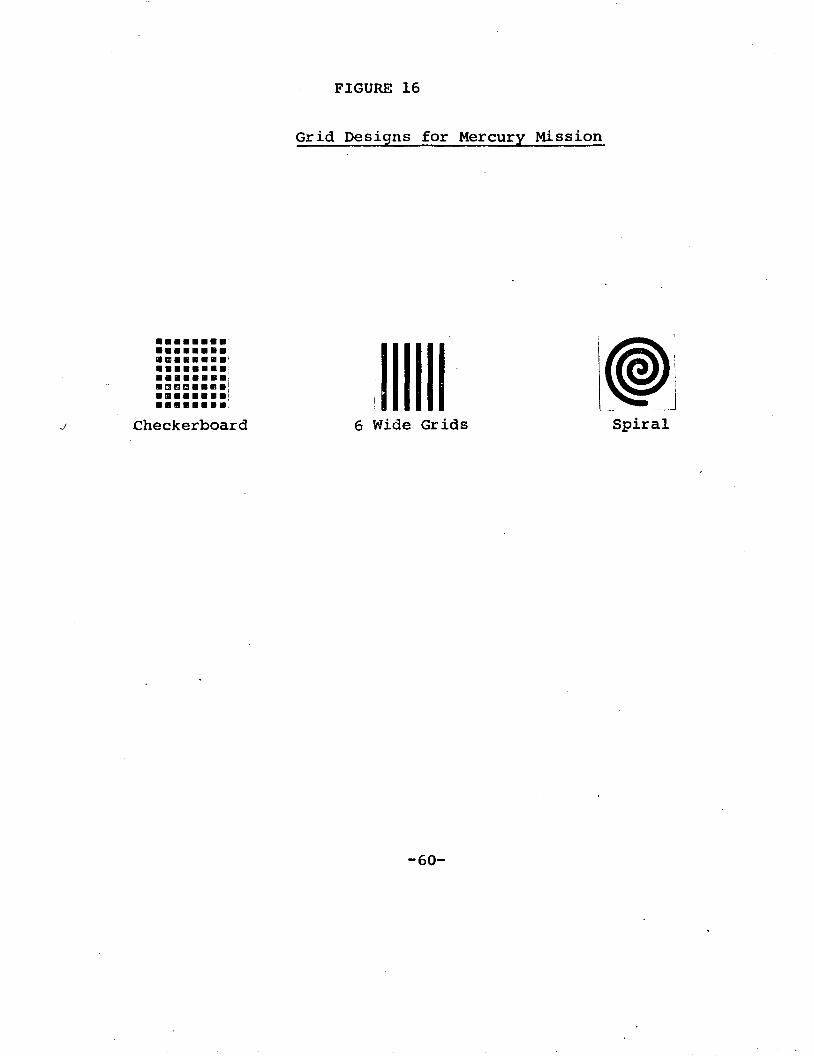
FIGURE 16
Grid Designs for Mercury Mission
••••••••
JIIIII '~,••••••••1111I •••• 11I.'••••••••......... ,II III IIUI •• II.:.11 •••••• :••••••••• ___J
.j Checkerboard 6 Wide Grids Spiral
-60-

TABLE 15
DESCRIPTION OF DELIVERABLE CELL GROUPS
, .
I GROUP SILICON JUNCTION BACK GRID TARGETDESIGNATION RESISTIVITY DEPTH CONTACT CONFIGURATION MISSION
(ohm-em) (1JIll)
#1 0.8 0.7 Ti-Ag Checkerboard Mercury
I #2 0.8 0.7 Ti-Ag 4 wide grids Mercury
I #2S 0.8 0.7 Ti-Ag Spiral Mercury
I #3 0.8 0.5 Ti-Ag 10 grids Venus
#4 2.0 0.5 Al-Ti-Ag 4 grids Mars
#5 5.0 0.7 Al-Ti-Ag 2 grids Asteroid Belt
#6 5.0 0.7 Al-Ti-Ag 1 grid Jupiter
#7 20.0 0.7 Al-Ti-Ag 1 grid Jupiter",;
Controls 2.0 0.4 Ti-Ag )f6 grids Earth
Controls 10.0 0.4 Ti-Ag 6 grids Earth
,-
-61-

6.0 MEASUREMENTS
A large part of the program involved measurement of cellproperties at various conditions, and analysis of thesemeasurements. Fuller details of the test equipment andprocedure are given in Appendix A.
6.1 Measurement Facilities
6.1.1 Routine Equipment
The following routine equipment was used:
(a) Solar simulators (tungsten-xe2on plus filters),giving AMO spectrum 140 mW/cm. Cells could bemaintained at 28°C ± 2% during test, and all thecells made were tested under these conditions.
(b) The forward biassed and reverse biassed I-V charac-·teristics of the cells in the dark could be measured.
(c) On selected cells, spectral response was measuredusing a filter wheel.
(d) On cells typical of the various groups, PN junctiondepth, sheet resistance and series resistance weremeasured.
6.1.2 Special Equipment
Some special tests were run specifically for this program.The tests were:
(a) A performated light box which2fitted under the solar
simulators, providing 5 mW/cm •
(b) A tungsten iodid~ lamp giving high intensity, approximately 850 mW/cm •
For both (a) and (b) the cell temperature was maintained at 28°C.
(c) During the course of the program selected groups ofcells were checked in the JPL measurement facility.
6.2 Summary of Measurements
The following Tables 16 and 17 summarize the measurementsmade on the cells.
6.2.1 Mission-Design Cell Groups
For the mission-design cell groups, Table 16 summarizesthe I-V characteristics (Pmax, Isc, ¥oc and CFF), forthree intensities (140, 5, 850 mW/cm ), all the cells heldat 28°C.
-62-

·T
AB
LE
16
SUM
MA
RYO
FI-
VM
EASU
REM
ENTS
at
28
°C
MIS
SIO
N-D
ES
IGN
CE
LL
GR
OU
PS
Inte
nsit
y-
(mW
/em
2)
,.1
40
58
50
IG
rou
pC
ell
iPm
axIs
eV
oe
CF
FP
max
Ise
Vo
eC
FF
Pm
axIs
eV
oeC
FF
Para
mete
rs[(m
w)
(rnA
)(m
V)
(mW
)(rn
A)
(mV
)(m
W)
(rnA
)(m
V)
IA
2o
hm
-em
18
44
.5
55
0.7
40
.21.
.33
50
*-
97
21
55
90
0.8
0*
x.
-0.
41-!
mch
eck
erb
oard
+1
4.5
43
.55
50
0.6
00
.11
.33
77
*-
12
0.5
26
06
02
0.7
7I
-
II
.A2
oh
m-e
m2
457
56
00
.75
0.4
1.5
43
0*
-1
42
30
65
90
0.7
8*
x.
,..,..
0.41
-!m
J6
wid
eg
rid
s+
18
53
.85
55
0.6
00
.3*
1.7
40
0*
-1
48
.53
26
61
00~74
II
B2
oh
m-e
m1
84
55
50
0.7
20
.31
.34
00
*-
--
--
x.
--1.
01-!
mJ
.6
wid
eg
rid
s
III
A2
oh
m-e
m6
01
34
59
00
.76
1.0
3.5
46
00
.62
31
77
60
61
00
.68
x.
/"-'
O.4
1-!m
J1
0g
rid
s+
57
.21
31
58
50
.74
1.1
4.5
47
0*
-3
20
.58
13
63
50
.62
III
B2
oh
m-e
m5
01
10
58
00
.61
0.7
53
.04
50
0.5
5-
--
-x
.--
-1.0
I-!m
J1
0g
rid
s
+=
JPL
measu
rem
en
ts*
=m
axim
umv
alu
ein
each
gro
up
-63
-

TP~LE
16
(co
nti
nu
ed
)
SUM
MA
RYO
FI-
VM
EASU
REM
ENTS
at
28
°C
MIS
SIO
N-D
ES
IGN
CE
LL
GR
OU
PS
Inte
nsit
y...
(mW
/cm
2)
,.1
40
58
50
Gro
up
Cell
Pm
axIs
eV
oeC
FFP
max
Ise
Voe
CFF
Pm
axIs
eV
oeC
FFP
ara
mete
rs(m
W)
(rnA
)(m
V)
(mW
)(rn
A)
(mV
)(m
W)
(rnA
)(m
V)
IVA
2oh
m-e
m5
81
40
59
00
.70
1.1
3.9
,46
50
.61
26
08
35
60
00
.52
x.
--0.4~m
J6
gri
ds
IVC
10
oh
m-e
m56
14
25
50
0.7
21
.04
.04
45
0.5
61
60
86
05
55
0.3
4x
."-0.4~m
J6
gri
ds
VA
2oh
m-e
m5
91
42
59
00
.70
-3
.74
25
--
--
-x
.-.J0.4~m
J4
gri
ds
VC
10
oh
m-e
m5
41
48
55
00
.67
1.0
3.9
43
50
.59
--
--
x.
,...,0.4~m
J4
gri
ds
+5
4.5
14
75
50
0.6
71
.55
5.0
45
50
.68
18
8.5
85
05
80
0.3
8
VI
B2
oh
m-e
m5
01
20
59
00
.70
0.8
3.0
45
50
.60
--
--
x..-
'1.0~m
J2
gri
ds
-64
-

TA
BL
E1
6(c
on
tin
ued
)
SUMMP~Y
OF
I-V
MEA
SUR
EMEN
TSat
28
°C
MIS
SIO
N-D
ES
IGN
CE
LL
GR
OU
PS
Inte
nsit
y... ,.
(mW
/em
2)
1.(
)A
i()
Gro
up
Cell
Pm
axIs
eV
oe
CF
FP
max
Ise
Vo
eC
FF
Pm
axIs
eV
oxC
FF
Para
mete
rs(m
W)
(rnA
)(m
V)
(mW
)(r
nA)
(mV
)(m
W)
(rnA
)(m
V)
VI
D1
0o
hm
-em
47
12
05
50
0.7
10
.83
.04
35
0.6
2-
--
xj
.-.-
1.01
-lm
2g
rid
s+
45
12
1.5
54
50
.68
1.2
4.1
54
45
0~64
16
3.5
69
05
75
0.4
1
VII
B2
oh
m-e
m4
21
18
58
50
.61
0.9
3.2
46
50
.61
--
--
x.
--1.
01-l
mJ
1g
rid
VII
D1
0o
hm
-em
40
12
65
50
0.5
80
.93
.24
45
0.6
4-
--
-x
.-
1.01
-lm
J1
gri
d+
37
.21
23
.55
45
0.5
51
.05
4.2
44
50
.56
10
8.5
52
05
70
0.3
6
-65
-

Isc Values
For 140 and 5 mW/cm2 , the observed Isc variations can beexplained by one or several of the following reasons:
(a) Variation in active area because of the grid patternused. The extreme case of small active area is seenfor the checkerboard design; in this case the activearea is less than the planned 40% because of somesplash-over of metal during evaporation. A largeractive area than normal is seen for 4 grids and less.
(b) Variation in bulk resistivity. In general, 10 ohrncm gives higher I sc •
(c) Variation in junction depth. I is decreased byapproximately 20% when the junc~ion depth is l.ofmrather than Oo4~m. '\
Voc Values
These were generally as expected for the bulk resistivityused. However, cells with inferior characteristics oftenshowed large decrease in Voc
CFF and Prnax
The CFF values at 140 mW/cm2 are useful to predict thehigh intensity performance. For example, groups lA, ~IA,
show promise. However IlIA had good CFF at 140 mW/cm ,but lower CFF at 6 suns. This shows that the 10 gridpattern alone was not sufficient to offset the reducedCFF resulting from the shallow junction.
Selection of Cells for Inner Missions Simulated Tests
For actual inner mission tests, based on overall I-Vcharacteristics, groups lA, IIA, lIB, IlIA and IIIB willbe compared to group IVA.
Selection of Cells for Outer Missions Simulated Tests
The CFF values for the groups planned for the outer missionsshowed that the following groups are worthy of more detailed testing. The groups to be compared with IVA are IlIA,VC, VIB, VID, VIIB, and VIID.
Dark Diode I-V Characteristics
It was hoped that for the wide variety of cell parametersinvolved, measurement of the dark diode characteristicsmight allow some information to be gained, to check thepossible operation for the various missions. In general,good correlation was found, e.g., deeper PN junctionsgave better reverse characteristics. However, specificcorrelation between the dark diode values and the various
-66-

I-V measurements at 28°C was not always obtained. Figure17 shows the percentages within the mission-design cellgroups which had designated forward or reverse characteristics. There is generally association of properties,i.e., good dark forward behavior is accompanied by gooddark reverse properties.
Spectral Response
Measurements were made of the output of typical cells inthe mission-design cells as ten narrow band filters weremoved in front of an illuminating tungsten lamp. Theratio of the output in the ninth' and second channelsshows how the ratio of long wavelength to short wavelengthresponse changes. These ratios are shown in Figure 18.The ratio is seen to increase with resistivity (becauseof increased long wavelength response, because of greaterbulk perfection) and also with deeper junctions (becauseof reduced short wavelength response).
6.2.2 Matrix Cell Groups
Table 17 summarizes the matrix cell groups under the sameconditions as noted in Table 16.
Isc Values
Again there is a decrease of around 10% in going from 10to 0.1 ohm-cm resistivity. In addi~ion, the deeper junction ~1.6~m) reduces I by an additional 20%. At 140mW/cm , as expected, n8ge of the ungridded cells show anypromise.
Voc Values
Again these are as expected from the bulk resistivity,and as before, poor cells often show low Voc
CFF and Pmax
Comparison of CFF values at low or high intensity againgives a guide to groups worthy of fuller investigation.
Selection of Cells for Inner Missions Simulated Tests
The groups showing most promise for the inner missions are3A, 3B, 3C, all incorporating deeper PN junctions and 6grids. Cells from these groups will be compared to GroupIVA in the mission design cell groups.
Selection of Cells for Outer Missions Simulated Tests
Low level readings show that the lack of grids does notprejudice, low level operation seriously. The followinggroups had good low intensity performance, and sample cellswill be compared with IVA, namely groups lC{or ID), 2C(or 2D), 3C{or 3D) and 4C{or 4D).
-67-

-
f Ii! II ! II I I I, I, I, I I! II! f :,d~'~I: ! II l' - j - ; I' ! I ! I 'f I II, -.~-1!'-i I L'~!l-l-TJ-I I I i I I I I I I I I I' ~ T\ !]J..,I --_of j, I - I., , . 'I J ! I - - -I 1 I: , i, I "i' : I " ! I I~ ~ 'T ;: 'i I I, I I '!: I ! I I ,,' i' 1'- ~ ~ j
, '" " ,I" , " ' ,I", \ I ' , , I I I I [J, j I I I.;.' ~; I~__ .......__ -Ll-.. : : 11---.:;: ;~. j: 1 I : r I; ,·1: i ;-;;! t: 1!- j --I I~i- r-j-:--!
~; : i I: !: ;+:+-"---:~','-, ;-: ~ti!1 j~;~~:~~~iri~~~=~rJ~~~ f144 1 --_ft-! ~II~ II I, I, t-!, i-l,'-j
1:1 : ' ,- I;;: i;': I !j'"'t ,I; I --, 'I I; ; I ! ",----+-\ " I ii,'I I i I : I I I ,! i! I i I I i I ! i I Iii I i \ I Ii I
g i !;' i : \ I I:, Ii, : i :1 'I I 11 I!! llll,'lll j! I 1- Lj!-~j~-t-,\,-,i _'IIIi".J I I I ! i i :: I :! i: :!! i [II', I ; I I' I I' I, --I,-J-"-'", ,'I 'il obi''\ I I: iii I : Ii! :',; i I i I f i 1.,'- H ': I- -- I
J~ J i;il--:-t!, ii--+-i-f-c
Iii I' I I -l'lf '
j f; !!' I !! II ': i, II, II iii I r I H· ..•·::rli4: I: f::! i: I i I; i III jl 11 I i I III I[ '111111111--,11 I II:~: I ;' ,'i i i !iiiiii i ·1 ! I I I' ! I I 1-1 11- i' ::
100 i' f--; i ~+-- '--c ': I " I ; , Irl; 1"::1", I r I' i 'I ,I, i~ j :: iii' iii: i: it, III 'i -,-r, 'I (- - I II Ill! 1 : -: 't"!" ' : : i ,f! i
.) ;' i i : i ; I " I I : i \ I, ' if' f 1 :' I I: I \ I --,I f I: i I \ \ ::80 ~'i ; I ' : ': ! :~-Tl !! ! I, I I ! I ! 'II 1' __ 1111 I ITT f I! ,I 1- Iii I-Iii
'Hi' I I ,II' I: !I:I :'I:~ i I 1111' II iii, ' i ,1- 'I ,t·,I' :" I I jJ' i"'O i I ,; I! i +t+:' \ -- "i, :1 1" _1
61 ' ~I~ "':-- '1-' +_.- - [/(f'----:-:~; ;-- --: -~~-~ %T:: : ~i\1 'I' '+-"--[1rilll
l,' i: i i 111 I lPf~ I+-r
l,Jr
.). '1 :; r: i~.! I! i '!, i illl II " i 1',11, [I I, I, L~ 'I,'il, ii, li'il,I ' I',": ~ ", '1\' iii I -- "Ii-
40 '~'~~ ~ 'I : I: IT:! i I -1,-1: I I \ II i ,: II j : I 'JI "lIvV'! ,,' iTT I1:i I
u ,rr' ,I '" ,,' I' I I' 1-- -j'II, ',' ~: II iJJ... ,., '-ll' iii I i j I",'I l-l ' .! , ! I I" ! i 1- f I, I I ,t-' I i I I VI __ I.J - l'j Ii' ;! ,j'
20 "g:T -~~~+:: i: ;;i: i ! : I mI Ii! I t\.[,tl'ii ill 'I· r1 n~rn ii, , ' I ", : i i : i ; , ,I : ! , Iii I; ill "I I I 'i ,I l' -j T i 1-1 I !I
o _ i ,r-: ;: ! !: I!: ~~~i i i !: I ii' 1" 'I! If 'I' ,i i Ill-i f I ! l~ - I,: i Il'I' ,j if Ii, Ii i i ,-I: :'il iii, I i-I!--TIII' ld-jii" ii':!
9 ' :':, ~,; i; II':;' lilil l ~ jill 'Ilil l'illlil'-!!II--i:"I:~Q ~ , i, I, !! III I, ! I I, Ii, 'I 1'- '11:' Il- t
C'1 ~ "'" : I I: i' i! i I I! lit Ii,: I ! Iil rJJl1 I! Ii,r·~---I----:-+~· ': ;;! I :: i III! II! I II' III i !! I ITii i III 11 i ! I ! i' 1: j'j~:: ,! : ! 'I' i! i : i I Ii U', I: I:: ': 'Ii i 'II I·!: I ,I J:
loLA.. I I I j I I I I I I . 'I I! Ii' I I I I : I L I U I I U I I I I100 I~-"i-'-'-----~--'-,--1---,,---'- -,·,t',--;- -~II --;-;--~' t--;-- _dl,-rt : t: I ;" ..........!-I-1-I-\ j-T-~ I ';"--r-, ~-;-~-
o ' l' "",: t, '. I ' ',:' .:; I' I ",' I ' ": 1 ,- :-Itii : : . I I ~ ! 1 ; : 1 ! : I Ii! i I : I !: i ! f ill ;. ~ !-: I! i·!· I .'-I~ :: I:! 'i i !: '!' I: ~:f:I~' IFie ~Jal~c ; j ,I,: j i! : i : i I -- ,J--l'oi : II
80, ... : "I " ! I: '~ i: ! II I Ii If ! Ii:, ,:! I I_I I I 1 fl --- '_"II -'I;")1I'L 1::
~I, l, I:,: ,.1 I II !. j, i I :"! 'i I I I'! I, I , " I'! I"", , I I I - I . I : ':
- ,'- : ,! ii': :" I" ' " ill' i ,: ' " I I ! ",- I - - -- , I - t ' I; ~ i ; t I I ,I i !; I- I I :' :. [ . L I I til " I;: I' l 'I . I ; I 1 i l!
60 I\~t-: --;, --;TT- --i-Ij-:r;-7"1'T:' -'7-;-~-i-- -1-TTi--~mti.: 1-; ~1TI· ';"'1'7~ -I-IiI' I-;-~-t ,i I'~' < I;:i', ,:!:. i,ll' 1"11' :li;lM:1,';' . II: 11'11 ;'"i, I'ii, I I I' I",
.!fl: :; :' I: II, I I! I 'i': I j I I' i 'II! I'!' ,I I '.j' ,'- r ,...~, i ;V]'~ .ID
....,-', ': ;:;; ! I I I I i I !,:: i' I ,1 J I Ii, ,I, I! lA' I i I . t I I il!' I I ' :,:
40 ~ I, i:, ,: ,J, ! I, ~:iii ~,I: i I rr,i! "III 1 i~' .I~I' i r~1'rff'rtilli:, : i m~LII~',1 i ItfJfj l~ ,i-! : I, :
riii. L'li l I:! IIN.! II uull "'Iii I" 'lIliilJ.: 1 t, Iii ii"~;_LI_, Ll.LI-~~ Ii, I l~i.II I~, __L -'-~ ili\ Ie I , j, j ,.NII" ' Ii,: '
20 ~ ! I r : Ii' I' -, I I il': i. I I I I~ 11: i,* Ie I 'i: i f I I "'!'T--'G ~-~--
~ !t i ill.; iE ! i ~ ll~ iii iii I: 1 ! iOil !° I111 1 i_U " i I
o ;:; i r.ii t:D] .IIi :~ J .I~ I I I : i I: I! I i I I I I I :: i T 11 i I I I I' I....' 'I 'I I I I I I I' ,;, i I I : ',: i" I j': iii' I I Ii ',', ' I,.. \ ii' I I ".. ,I I ' -, j I' I I 'I 1 I I I
:, j I !.; I I I I f I , ! J I I !!: I i! iii I ,I i . j. t I, !+! I ~ i i: i '
-'~~-r-;-;:-", ; 1 t - I! t ;1jT Tm- 11 l. I, II! II.)! TtTT ~I--iTT I i 1--1' = I II ,--c-,:; _.:-_-: -:. +IJ i 'l Iii 1 I i \.'[ 1- I I' I I, -! I I " I I ,- I I ,- I -
, : : "[ : I,· \-t·· i j I • : 'j I· i .,',' r j' j j ; I I ' - t I I' I ", I-I ' Iii ,I ' :, ,'.. , r ! , i - r I r : il r i 1111 I H ~. I; If! i IT r :'i-I I i iiI I I, !
M~ss~on Des~gn eel Group
-68-

! ! Iii II' II I, 'I: ! i i [' i l·f'''t(rlf~TIlTTlrr =tlT~Trl!·! r 'II 11- -W-I---j--!: 'IL
: +.ii-':111 1 : "~,I ,I! I, j.'l f 'j!!lll-.j-·-,"TII'llli,11 -H.t.lill-I,l-JiLl Ll i I iJl,...W- iii: : i II ~i~ , :> bfl '.~,R~ .-4k' i ~ -']1 J~j[-&,e+-H- -
! ; i: ' ., 'i I I !1\ 1 t-~lC~ ·+1 f~~ll~t; ctet: ,_~J, ~l~j I, I. !, t- ' , i - "';); ,_'IIo7a. rll!-:"'rn ~ ..1 r ! ! I I !
-' iF ~ i j 'I ' I, '·',rvr -,- I I !', If.!; ~ I ; I ii' '. Ii - - -! -, -- -,- I I i I I
-' 1:1- l=:J ,i j, : 'I 1_ I j ,i; ----1-1-' T,-- ,~-I- --I --I - --1,--- __.+1_;1------ . ~~:!: I j I j ('! ! Ii I'----:j--j-'TT' 11'1 !+:-~: -[1'--·-·- 'i:j:l~l-
I I~ ~I iii[il-I- -I i ,-I, i I ; -H-I, -1---' --T--' -f- I-Irl't-rti' ~ ji _! I r,I I' l I; I ) I I 1 I 'j' II! J j" "t·- +1' -1 1 : 1-11
: ! i; :,' i : ; I r I' 1,'1 i I I', ii, '11
I" r -]' - -:-I-rr. -ji,il'l: . i i~ ~i i, ; I,! \ i: ; " If,fi 1'\ f \ .. , - - '--,' ';' IT:- - '-.;-- r--~i+H--H-++-+-H--I-+++-t-+-+-H-+-I-++-H-I-H-++++-H+-I-+++-H-+-H-++++-H--I
i '! !i~' : i ': 1i ~: Iii [ )1 J 11, I jJj~ -j''I'l L-I/,! II .j- -f-]I 1, I i
l,!::,- .~ i, . i !; "! I I !'I I! I I II 1-'/ [ ;, I ,L" ' , .. ~ ., ,I ' ". -,I
I" I ,.. ~,. ,,' I: , 'I I I I· ,I : - - 1-I !. I 1 t L. r' 1 L _1. __ '''1-
3 2 ...1.--'--+-~ ~...4-~ -+-~--+ I I-'--+---'--+- 1_,_'-: "'!::' , !; ': I ' : '! +-r-o i:~'g:'! Ii! "i 1::1 1111i1j[ 11.
11.[ III J~r.-J-=-jl)... I:t.i
i '~JM:, ;1 '~! iiif itli iii lill '-li:1p:~(~rri-ij-13. 0 -,---~ -,_. -1--1 , ' ,
, '~" i ' : iii I I ! j Ui II i I I K $J·f") II'" ... ' ... i·,,+·4 !: I • :,' i Ii
[
'I :0 'i l '! il!i I_t' --r-!il ',. -t-,'-r"'i"T--- ---'I' -"l:i i" , Iii, I j'1-41 ' 1:1" I :4"- 'I' - " 1 I' ; I! I
2 '8 _I U..J8_~,---~~. : ' "i.! J.J i _ -~f+U c-, . i ' , -I-', i i.-l- j., It- ; ~ I :~ll~ i ! ~, : ;! r'-~T :; i! I i I I i I 'I I ! I :! 'I ii'''' '1- , !!! i \ "1' 'III j' n ~ P~'i) \
, ' 1!1t! ,I , I , 'i ! I I I I', ' Iii' I""" , I' I I ,- -- I 1-1 - , ..~ I, , N', ' , :' ; I ,! ; Ii: I", I. i ' [' 1 II I, . -- - -II Lt.' 'i 'I I ..... I I I I Ii, I Ii, I II I, ~ I I I' J I I f I I I I, " ' " I'!' ; I J I 'i I I : : I - J : 1 -- - --- - 1 1 - 1 '-r-- ,- -,-J...J.. -'-'- I ',. ,II" , , , ' , I .-;- ....~
2 •6~ , : ~,-~ : 1-;,,: 'i! '.: Ii! /1T! If iIiil, 1 ! 1] L, .. I" 1'1'+:I -J I., 11
:, :" :;:::' i i: I: i i II'1- ,i " r I I - :-:1 1 II r-rr -I 1-11: ' 1
.4 .-,.,-. -,--,--'-;-;-.--,----'-j- -'.!-~--.; I-r-j- I-:T ,'," I!' t-t-I-- H'I ~- ill 1- -, 1,'--;-', : " "1 ' i ; i ! ~ ~ ; I 1 I I II' ' I - 11 Iii I ' I : ';
,'; 'I . I' I", i i : I 11 I' I ; I I I II' If ' i I' ,I I' I 1 I, 'i ': I I "" I Iii WI I I 'I I I ' 1'1 I 1- : I I! I
, , " """, ,I I' Ii' I ii' ,-- I - ., - -I - 'I' i" 'I I I I I ' I I I I I I I I I iii
2 .2 -- T --- I:' I.' ; I ! i II; ! ! i 'j I!! 1,,- ,_ j- II I iii ! -I! ! I II ' i I I! I I.
I I, I' ':' i : ~ " Ii, I',', ,-- I 'I i I I. 1--' I ! I I : I ,I! t ~ , • I' I I ' I, 'I I I I I I I I
: : i ., ~: : ~. . i" : \ i I /' L. i: I, I \ i II II ;,. " I 1 t 1 i 1 Ii ii' II _'ii L..l 'i' j ~;, 1" ,,' i '! Iii I I Iii I I I I i ! ,I i I I Iii i 1-- i I I r llil - ~lri'2.o.,...r---~~--'-~~+.-~--:-:r~----~~',: :1"" --,T! i--~rn~T~i -f Ii WII r~~q I[ r UI,- ~l~" ':j 111. frt
'-, " '.:: I '. ,.. , '. Ii. "I I,:' 'i!' I -, --, 1'1"'j ,.,j..o1· I 1 -- , ,. -+1'" ,:'" j !,',':,; Ii' JI i' ii' ;" ;i l' II L. 'I' I "1· I-L- ...' - ".1...;.,, , I I " . f-' ',I I I r I I I I I I "'", i ~ - [I ' urn: J
1.,8' --:.--', ---;--:-1-;--1' ' ! i :: ,~'i T '0r-t"": i lit.! i. I,~"l .,~j.)CI_ i-'H' :r.: ! I! 1-1iii 7'. . ! , :, : I I I : I I I t' ,I I I ! I , I I ! ~ t ' -,,~ I I I I,' I. 1 1
1 ,',' • I' .'," i' I:" I I I· I ' ,.,.. " I' 1 I,' ,I
: ,; i: i ' : I iii " :,; til iii 'I t i i Ii, 'IA'"Iii i : i ',I I I I I I: ; 'i: i I .: r I !;!! II!;: I i I -i I'; II I -I'j-'I +j'; I ! I : 1 : L lil: i I!l.T.-:-.--;--t- -i-;--i~-; -'.' -T-:.<'- T:--r--t-- J:i~T TiTt P-i T ~.I',II ...... 1 i il iii' ITtr'I-: H
I,,- I I • -------;-
:. ' " ,I.:: - I I ! I ,;, i ~; I: I I I I ,! 1 I J(' I I, i! [I 'i i I I i I I: • •.. • I I' ! I I' 'II! t~! l;ikJI, ! I, I I '~ I : I ! ,I I I ": I' i: : I Iii I I I ;!' ~i J' :~ i II iii iATil I. r: I i' ! i! i I1 4, ' ...:.-- ~!-'. --j-' , I til IJ, "', ' , , , : , L..._ ~,_
_ . --I I I. I. I I r: : '. I! I;: i II' I I ,I tJ I. rII I i I I I!!! ; I I II I I: I!:! III i i;:; "II I r I ! I I: I 'I W',II, I II I, l 1 ,i,'! i i! iii i ; j! I I tl i! 1 Lil ;./-1 I : iii i HI! I I I , ,11 I ' I Ii; ,
lo2iinnrrTil" ~lnJ~,rlJJJ rWlil1 lilt!! i i 1111 11 1 i It: rH-i-1 .0 -;-- 1"--:-1.- --to i TTl'. I.! ,I!' 1 I' I I' I" I I ;" I I 1 ,I l' " "
I. j I I I, jl I I i j -'I· I' - i! 11: 'I' I, [I I I ,"I II; I' I I I I I I I I I '
T I I i I I I I 1- -j--- I ,-, I! If" ,I I'! '-- ,Iii 1,1 Ii'" 'I' +I, ' 'i! I· ,I ' !o•8 I I ,__ I ! ! _ !-Lf- ii', I!'. i .
-t It· ~ I ! \ \ I) 11]: J-I, I: \' Ij I F,it ~l j'l -il U~ i ~II- f- ,
, • L i ~ '- I, i -f! ; t - j i I'i I '. I til ill I I " . ., - i "·1', --!-'1'1 r L i ;' r-r 1 "i i I: ,I iii i t I I 1 Iii - rl i i'--I ~- Ii I' !o•6 '-"-~~~'-'-'-'-,~'-J-~~t-::-"-'-"-'-"-'-'-"""'-'--'--.l-..l--'---:-'-:-"--'-'-'--'--",-,-"""''''''''''''''''''''''~~..l-.L..L...I....L...I...!-.l..J
0.1 1.0 10Log /Resistivity (ohm-em)!
" flQ "

TAB
LE17
SUM
MA
RYO
FI-
VM
EASU
REM
ENTS
at
28
°C
MA
TRIX
CE
LL
GR
OU
PS
Inte
nsit
y-
(rnw
/ern
2)
.1
40
58
50
Gro
up
Cell
Prna
J<Is
eV
oeC
FFPr
nax
Ise
Voe
CFF
Prna
xIs
eV
oeC
FFP
ara
mete
rs(rn
W)
(rnA
)(rn
V)
(rnW
)(r
nA)
(rnV
)(rn
W)
(rnA
)(rn
V)
1A
0.1
ohm
-ern
551
26
60
00
.73
0.8
3.4
40
0*
0.5
92
75
52
06
30
*-
x.
-0.
41lr
nJ
6g
rid
sT
i-A
ob
aek
1B
0.1
ohm
-ern
55
12
65
55
0.7
90
.53
.43
00
0.4
8-
59
04
90
*-
x.~
0.41
lrn
J6
gri
ds
A1
-Ti-
Ao
baek
1C
10
ohm
-ern
551
39
55
00
.72
1.2
3..9
46
00
.67
18
5*
89
05
70
-x
...
-0.
41lr
nJ
6g
rid
sT
i-A
qb
aek
1D
10
ohm
-ern
571
40
56
00
.73
1.2
3.9
46
00
.67
-8
50
46
0-
x.
...-
0.41
lrn
J6
gri
ds
A1
-Ti-
Aq
baek
2A
0.1
ohm
-ern
10
50
58
00
.35
0.8
3.5
38
0*
0.6
01
9*
10
05
65
-x
.--
-0
.41l
rnJ og
rid
sT
i-A
qb
aek
*=
max
imum
valu
ein
eaeh
gro
up
-70
-

TA
BL
E1
7(e
on
tin
ued
)
SUM
MA
RY
OF
I-V
ME
ASU
RE
ME
NT
Sat
28
°C
MA
TR
IXC
EL
LG
RO
UPS
Intensi~y
-(r
nW/e
rn2
)-
14
05
85
0
Gro
up
Cell
Pma:
xIs
eV
oe
CF
FP
max
Ise
Vo
eC
FF
Pm
axIs
eV
oe
CF
FP
ara
mete
rs(rn
W)
(rnA
)(r
nV)
(rnW
)(r
nA)
(rnV
)(rn
W)
(rnA
)(r
nV)
0.1
oh
m-e
m8
50
56
00
.29
0.2
2.0
20
00
.50
"~
2B
-9
54
20
-I
X.
---
0.4J
.lrn
(
J og
rid
sA
I-T
i-A
qb
aek
I2
C1
0o
hm
-em
10
50
55
00
.38
1.1
4.2
46
00
.57
10
04
75
--
Ix
.--
0.41
Jrn
J og
rid
sT
i-A
qb
aek
20
10
oh
m-e
m1
0.5
50
55
00
.38
1.1
4.2
36
00
.57
-8
55
00
-x
.--
0.41
Jrn
J og
rid
sA
I-T
i-A
qb
aek
3A
0.1
oh
m-e
m5
01
06
60
00
.80
0.8
2.9
47
00
.59
25
05
20
63
50.
75>
x.
....-
1.61
Jrn
J6
gri
ds
Ti-
Aq
baek
3B
0.1
oh
m-e
m5
01
06
60
00
.80
0.9
2.9
48
00
.64
23
05
25
63
00
.70
x.,-
1.61
Jrn
J6
gri
ds
AI-
Ti-
Aq
baek
3C
10
oh
m-e
m5
01
20
55
00
.75
1.1
3.4
46
00
.70
.29
07
25
59
5*
0.6
7x
.,-..
..;1
.6IJr
n6
Jgri
ds
-A
I-T
J.-A
qb
aek

TA
BL
E1
7(e
on
tin
ued
)
SUM
MA
RYO
FI-
VM
EA
SUR
EM
EN
TS
at
28
°C
MA
TR
IXC
EL
LG
RO
UPS
Inte
nsi 2y
....(m
W/e
m)
,-1
40
58
50
Gro
up
Cell
Pm
axIs
eV
oe
CF
FP
max
Ise
Vo
eC
FF
Pm
axIs
cV
oe
CF
FP
ara
mete
rs(m
W)
(rnA
)(m
V)
(mW
)(r
nA)
(mV
)(m
W)
(rnA
)(m
V)
3D
10
oh
m-e
m5
11
20
55
00
.77
1.1
3.4
46
00~70
67
77
04
85
0.1
8x
.-1
.6j.
.lm
J6
grid~
AI-
Ti-
Aq
baek
4A
0.1
oh
m-e
m2
09
06
00
0.3
71
.03
.24
70
0.6
75
02
40
59
00
.35
x.
...-
1.6j
..lm
J og
rid
sT
i-A
qb
aek
4B
0.1
oh
m-e
m1
78
45
90
0.3
40
.73
.14
00
*0
.56
19
11
05
35
*-
x.
.-.1
.6j.
.lm
J og
rid
sA
1-t
i-A
qb
aek
4C
10
oh
m-e
m1
99
05
50
0.3
81
.23
.64
60
0.7
2-
23
04
40
*-
x.
--1.
6j..l
mJ og
rid
sT
i-A
qb
aek
4D
10
oh
m-e
m2
09
05
45
0.4
11
.15
3.6
46
00
.69
-2
40
45
5-
x.
.-..
1.6j
..lm
J og
rid
sA
1-T
i-A
qb
aek
-72
-

Dark Diode I-V Characteristics
Figure 19 shows a plot for the matrix cells correspondingto Figure L7. Again the percentage of matrix cell groupswhich had given forward or reverse characteristics, isplotted versus the group. The same association is seenas in Figure 16.
Spectral Response
Figure 20shows a plot corresponding to Figure 18. Thesame trends are seen. The values for the matrix cells arealso given in Figure 18. Figure 20 shows how I at AMOvar ies for bdth groups of ce.lls, as the junction depth increased.
Anomalies
In the course of the work, several anomalies were investigated. These included:
(a)
(b)
(c)
The occurrence of very low V for matrix cell groupswhich combined low resistivi€? silicon and a shallowPN junction. The probable reason was identified aspenetration of the very shallow junction by frontcontact metals during the sintering cycle.
Splash-over of contact metals when evaporating throughthe checkerboard, 4 wide grid or 10-grid masks.This splash-over reduced the active area of the cells.The reason was lack of close contact between thecells and the contact masks, and the remedy was toadd magnetic hold-down capability to the mask fixtures.
Wide I variations in some groups were traced tosurfac~Cstains, occurring as a result of incompletecleaning of the front surface during cell fabrication.This problem was not trivial because the surfacestains were generally invisible until the siliconmonoxide film was evaporated on the cells. The causeof the stains was subtle, involving interaction ofthe surface layers left on the cell from previousprocessing steps, and the acids (and their concentration) used to remove these layers.
The anomalies and their solutions increased theunderstanding of interactions between cell parameters,and also indicated where some changes in the fabrication steps can be made in future work. Wherevercritical interaction is involved between specificsteps, before cells are made, small scale separatetests are needed to decide on the best sequencewhich will minimize interacti.on and thus allowreliable evaluation of the effects of separate variables.
-73-

Ii I
I; :~- ,'- -,i . I~- .. i ,--' .. ·:·r--·~ ..-..·
! i 'U ..
19
D
F
1..__'_ ,.
It ..
i I I i
~_._.:... t-.~.....:-._.~ .. ~_l_."-_:.
_"2~t j __:2 L~L_~ _MATRIX CELL GROUP
- 74 -
0
11iI
1~i
i I JJ,
1.- _' •._1 _
.±1i 00-1
40 i ~.'+JI~1(1)'u
20 l'~:P-iI
I0 '"""IIr
iI
I~~·o·" .....14-1I.
100 i~1 Mi/\I.
80 f 'f%.l~ .. ;.I :> :1.I 0j,co.I+JMj
60 r°r+ . I ..I ~ 1\ .I f%.l !i+JHi. ~4 0 ~_~...__+ ._I u : .~(I)
P-i20
ri!~ r·:-- T-
, ' iI :
. " 1 . " I "1
~._-----~------ ..---l--·- -- ---~._-+-.,.......-+I I I I
I :>: I i: S I I! I
18 i I I I::
Ii~--f-- I ---1,...._.-_J~~I ~ I 'i .
10oH-1 I!-~! ;10, I I10 Ii! ..
80 ~-.-t---.~.--····~··_·--l·-·-·"-""·"·T-·:--"r:::c~~rllv' i iI I.~ ,
60 Hi.I
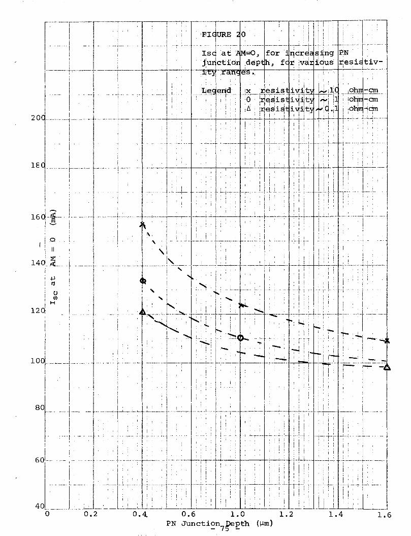
-1I
:'l..
l?N .llesi tiv-
.-'--..........~-'-<I----- -_._._-....
i16q·-~.-·- .
1-
,.1
I
I1001···---_
I80l __
I
II!
I
1°! /II
14d.~ ....i

7.0 CONCLUSIONS
Because the simulated mission tests have not yet beencarried out, conclusions can be made based only on thetheoretical study, the cell fabrication results, and28°C test results at three intensities covering thevalues at Jupiter, Earth and Mercury. Within this framework, the following conclusions can be drawn.
(1) As usual in solar cell work, it is necessary todesign specifically for each mission, including allthe mission requirements. For example, if tiltingarrays are considered the best choice for the,Mercury mission, the approach which was followedin Section 4 is toourr~ble. The use of a largefraction of reflecting metal contact can limit theamount of power available for the mission as thespacecraft moves toward Mercury.
Also, although radiation goals are not defined, itis clear that these must be introduced into anyprogram designing cells for a range of missionssuch as those considered here.
Also, practical factors (e.g., whether the arraydesign can accept unsoldered cells) must be considered.
(2) With the reservations in (1), the present programhas demonstrated that the present state-of-the-artcan be adjusted to fabricate cells with a goodchance of giving acceptable performance over thewhole range considered. This is particularly truefor the inner missions. Present day technology, incombinations within the range of parameters usedhere, is available to design cells capable of goodoperation for current array designs. The questionof whether all the outer mission requirements canbe met will depend in part on the detailed testson cells made here, and in part on whether theoverall mission needs can in fact be satisfied bysolar cells.
(3) There are often interactions between the variousfabrication steps and these must be known and understood, and minimized before realistic assessmentcan be made of the separate effects of the differentcell parameters.
(4) Theoretical calculations show that there should beno advantage in shifting the minimum of the anti
reflection coating to longer wavelengths.
-76-

(5) Spectral response measurements are helpful in understanding the trends in cell properties as the parameters are changed.
(6) Unilluminated diode characteristics were not asspecifically useful as expected, although generalcorrelation was found. However, measurement ofthese parameters at the expected mission temperatures could allow realistic predictions of actualmission behavior, because the detailed diode properties dominate the overall cell performance, oncethe external properties such as light generatedcurrent, series and parallel resistance are established.
(7) The conclusions on performance in actual missionconditions will be reported separately when thesetests have been run.
-77-

8.0 SUGGESTIONS FOR FUTURE CELL DESIGN WORK
As mentioned in Section 7.0, actual simulated missiontests have not yet been run for the variety of cellsfabricated in this program, and therefore final suggestions cannot be made until the results of these testsare known. The results of, these tests, when analyzed,should indicate some future directions to pursue.
The results to date indicate that the major area requiring further attention will be the specification ofprocesses which ensure that the excess current in the PNjunction will be IDW enough to provide good cells forJupiter conditions.
It has been emphasized in this program that beforemission needs can be met, consideration must be givento the total array needs, including the weight andmechanical needs, and also the radiation requirements.Some of the cells fabricated in this program will beuseful for such radiation tests, and will be evaluatedfor their radiation resistance.
-78-

9.0 REFERENCES
1. Drummond, A. J. - Precision Radiometry and itsSignificance in Atmospheric and Space Physics" inAdvances in Geophysics, Volume 14, Academic Press (1970).
2. Ross, R. A., Jr. - "Solar-Panel Approaches for a VenusMercury Flyby" presented at Space Technology and HeatTransfer Conference, Los Angeles, June 1970, ASME Paper70-Av/sp T-29.
3. Crossley, P. A. et aI, "Review and Evaluation of PastSolar Cell Development Efforts l' • Final Report, NASAContract NASW-1427, RCA, Princeton, N.J. (1968),Appendix II.
4. Olson, o. H., "Selected Ordinates for Solar AbsorptivityCalculations", Appl. opt. 2,109 (1963).
5. Francon, M., "Modern Applications of Physical Optics",Interscience, New York (1963).
6. Hass, G. & Salzberg, C. D., "Optical Properties ofSilicon Monoxide in the Wavelength Region from 0.24 to14.0 Microns II, J. opt. Soc.. Arner. 44, 181 (1954).
7. Runyan, W. R., "Silicon Semiconductor Technology",McGraw-Hill, New York (1965), p. 198.
8. Schmidt, E., IISimple Method for the Determination ofOptical Constants of Absorbing Materials ll , Appl. Opt.8, 1905 (1969).
9. R. A. Smith, "Semiconductors" Cambridge UniversityPress 1959, p. 350.
10. K. L. Kennerud, IIElectrical Characteristics of SiliconSolar Cells at Low Temperatures ll • IEEE Trans. onAerospace and Electronic System, Vol. AES-3, No.6,July 1967, p. 586.
11. J. D. Sandstrom, IIElectrical Characteristics of SiliconSolar Cells as a Function of Cell Temperature and SolarIntensityll. Proceedings IECED 1968, p. 138.
12. R. K. Yasui, L. W. Schmidt, "Performance Characteristicsof Ti-Ag Contact Nip and PIN Silicon Solar Cells:".Proceedings 8th Photovoltaic Specialists Conference 1970,p. 110.
13. R. J. Debs, W. R. Hanes, "preliminary Results ofRadiation Jupiter Environment Tests on Solar Cells" ,Proceedings 8th Photovoltaic Specialists Conference1970, p. 158.
- 79 -

References (Cont'd.)
14. P. A. Payne, E. L. Ralph, "Low Temperature and LowSolar Intensity Characteristics of Silicon Solar Cells",Proceedings 8th Photovoltaic Specialists Conference1970, p. 135.
15. J. C. Ho, F. T. C. Bartels, A. R. Kirkpatrick, "SolarCell Low Temperature, Low Solar Intensity Operation",Proceedings 8th Photovoltaic Specialists Conference1970, p. 150.
16. W. C. Dash, R. Newman, "Intrinsic Optical Absorptionin Single Crystal Ge and Si at 77 oK and 300 oK", Phys. Rev.Vol. 99, p. 1151, 1955.
17. A. Shumka, "Temperature Effects on Silicon Solar CellsShort Circuit Currents", Proceedings 8th PhotovoltaicSpecialists Conference 1970, p. 96 0
18. H. W. Brandhorst, R. E. Hart, "Spectral Response ofSilicon Solar Cells at Low Temperatures", Proceedings8th Photovoltaic Specialists Conference 1970, p. 142.
- 80 -
10.0 BIBLIOGRAPHY
The following papers contain information bearing directly onthe present program.
1) J. D. Sandstrom "Electrical Characteristics of SiliconSolar Cells as a Function of Cell Temperature and SolarIntensity". Proceedings of the Intersociety EnergyConversion Engineering Conference 1968, page 138. At JPL,measured N/P cells with 2 ohm-cm base resistivity, withthicknesses extending from 0.01 em ( 4 mils) to 0.045 cm( 18 mils). Also evaluated some pIN cells with 1 ohm-cmresistivity silicon. The cell temperatures were variedfrom -lOOoC to +lOOoC, and the s02ar intensities used were5, 25, 50, 100, 140 and 250 mW/em. I sc , Voc and Pmaxwere plotted both as a function of temperature and ofintensity. The performance of these cells decreased at theextremes. At low intensity, low temperature, Pmax did notincrease as fast as Voc , indicatin~ decrease in CFF. Athigh intensity, high temperature, max decreased probablybecause of the increased effects of series resistance.
2) R. K. Yasui L. W. Schmidt, "Performance Characteristicsof Ti-Ag Contact N/P and pIN Silicon Solar Cells".Proceedings of the 8th Photovoltaic Specialists' Conference,1970,page 110.N/P&P!Ncells of 2 ohm-em base resistivitywere measured under simulated Jupiter and Venus conditions.The intensity range used was 5 to 250 mW/cm2 and the temperature range was -140oC to + l40oC. Some mechanicalcontact tests were run, and showed a maximum for the contactstrength around -50oC to - 100oCo Pmax was measured forboth cell types as a function of temperature and intensity.The two types were equivalent at low temperatures and intensities, but the N/P cells were 4% better above l40mw/em2 •Voc increased linearly with decreasing temperature for intensities above 25 mW/cm2 • At 5 mW/em2 Voc increased moreslowly at temperaturesbelow -50oC. The C.F.F. was plottedas a function of temperature and showed a maximum valuearound -30oC. For 5 mW/cm2 CFF decreased for temperaturesbelow -50oC.
3) J. V. Foster, A. C. Wilbur, D. C. Briggs, S. Friedlander"Silicon Solar Cells for Near-Sun Missions". Proceedings ofthe 6th Photovoltaic Specialists' Conference, 1967~ page 117.This study divided into two parts, to investigate highlyreflective coatings and selective filters for use on solarcells at 0.4 A.U., and the design of solar cells capable ofgood operation at 0.2 A.U.
- 81 -

The narrow band filters were good at 0.2 A.U., but poor at1.0 A. U. The reflective coatings were not as good at 0.2A. U., but had a better balance from 1 to 6 suns. The cellswere designed to have low series resistance, by using thinslices of low resistivity (0.5 ohm-em), normal diffusion, andeleven grids across the 2 em dimension of the cell. Thesecells were superior to commercial cells above 5 suns' intensity.
4) P. A. Johnston "Laboratory Experiments on the Performance ofSilicon Solar Cells at High Solar Intensities and Temperatures"NASA Technical Note, TND - 2733, March 1965. I-V characteristics of N/P (10 ohm-em resistivity) were measured for hightemperatures ( to l670 C) and for high intensities ( up to600 mW/cm2). Severe power reduction was observed at thehigher temperatures. Measurements were made of the dependenceof cell output as the angle of incidence of the illuminationwas varied. This led to the conclusion that the temperatureof an array moving towards the sun could be reduced to maintain relatively constant power output, by gradually increasingthe angle of incidence for closer approach.
5) W. Luft "Silicon Solar Cell Performance at High Intensities".lEE Transactions on Aerospace and Electronics, Vol A ES-6,No.6, Nov. 1970, page 797. Tests were made of conventional5 grid silicon cells (10 ohm-em resistivity), special 13 gridsilicon cells (0.5 ohm-em resistivity) and a Gallium Arsenidecell, for illumination intensities from 70 to 2800 mw/cm2 1and for temperatures 300 to l500 C. The 13 grid cells showedsuperior performance giving good conversion efficiency up to20 suns (2800 mW/cm2).
6) J. D. Broder, H. E. Kautz, J. Mandelkorn, L. Schwartz, R. L.Ulman "Solar Cell Performance at High Temperatures". NASATechnical Note D 2529, Dec. 1964. N/P cells were made inconventional fashion, with base resistivity in the range 1 to80 ohm-em, and were tested at AMO, 140 mW/em2 at temperaturesranging from 250 C to 2000 C. Without radiation, the 1 ohm-emcells had most power outfut over the whole range. Afterirradiation by 1.5 X 10 6 1 MeV electrons per cm2 , the 10ohm-em cells had highest output up to l2SOC the 1 ohm-cellsgiving most output above l500 C Some tests with GalliumArsenide showed no advantage in power output up to 2000 C.
- 82 -

7) R. G. Ross, Jr., R. K. Yasui, W. Jaworski, L-C Wen,E. Cleland "Measured Performance of Silicon Solar CellAssemblies Designed for Use at High Solar Intensities".JPL Technical Memorandum 33-473, March 1971. Three methodswere considered to reduce cell array temperatures forapproach to 0.4 Au. These approaches were the mirror mosaic,the selective filter and the tilted array. Electrical andthermal characteristics were measured for several cell/coverglass array assemblies using these three methods. The cellsused were N/P, either 2 or 10 ohm-cm, with three differentgrid patterns, namely normal grids, four wide grids anda large covered area with open cell area near the edges.Detailed measurements were given of the I-V characteristicsof the various cell/coverglass combinations for intensitiesfrom 140 to 850 mw/cm2 , with cell temperatures between -40oCand +160oC.
8) C. A. Lewis, J.P" Kirkpatrick "Solar Cell Characteristicsat High Solar Intensities and Temperatures". Proceedingsof the 8th Photovoltaic Specialists' Conference, 1970, page123. Silicon solar cells, some standard production types,others designed for high intensity use, were compared overan intensity range of 1 to 25 solar constants (140 to 3500mW/cm2) and a temperature range 280 C to 200oC. The cellsspecially designed performed well, with efficiences up to2.5% for operation at the highest limits of intensity andtemperature. Some tests were also made on the effects ofthese extreme conditions on coverglass and adhesives and onthe variation of cell output with varying angle of incidence.Some Gallium Arsenide cells showed less percentage decreaseat the high temperatures, but their overall output was lowerthan the silicon cells at all intensity levels.
9) K. L. Kennerud "Electrical Characteristics of SiliconSolar Cells at Low Temperatures". lEE Transactions on Aerospace and Electronics, Vol AES-3, No.4., July 1967, page586. Pmax , Voc and I sc for pIN and N/P cells (1 ohm-cmresistivity) were measured from -196oC to +50oC under AMOintensities of 58 and 268 mW/cm2 • The objective was todetermine cell behavior for a Mars orbiting spacecraft.For the N/P cells, Voc ceased to increase around -80oC.For the P/N cells, Voc increased linearly down to -196oC.Speculation is made that the anomalous behavior of N/P cellsprises from recombination center or surface leakage currents.LIn retrospect it is possible that the observed anomaliescould be explained by the formation of a Schottky barrier~
- 83 -

10) H. Liebert "Solar Cell Performance at Jupiter Temperatureand Solar Intensity" Proceedings of the 7th PhotovoltaicSpecialists' Conference, 1968, page 92. N/P silicon solarcells (10 ohm-cm resistivity) and cadimum sulfide cellswere tested at Jupiter conditions (6 mW/cm2 , -1330 C). Thesilicon cells varied widely, with efficiencies at Jupiterconditions varying from zero to 15%.
11) R. J. Lambert "Characteristics of Solar Cells at LowTemperatures" Proceedings of the 7th PhotovoltaicSpecialists' Conference, 1968, page 97. piN silicon cells(1 ohm-cm resistivity) and N/P silicon cells ( 1 and 10
ohm-cm resistivity) were measured from -190o C to 27oC, atlight intensities from 1 to 140 mW/cm2 • Cell efficiencyat 140 mw/cm2 and -190oC reached 16%. At -190oC the cellsshowed signs of constant Voc as the intensity was varied.For some cells, Voc increased linearly with decreasingtemperature, for other cells Voc reached saturation, showingsigns of Schottky barrier formation.
12) W. Luft "Silicon Solar Cells at Low Temperatures" lEETransactions on Aerospace and Electronics Systems,Vol AES-7No.2, March 1971, page 332.[This paper also appeared inthe Proceedings of the 8th Photovoltaic Specialists' Conference, 1970, page l6i]. N/P cells were measured over atemperature range of 280 C to -1750 C with illumination intensities ranging from 140 mW/cm2 to 1.5 mW/cm2 • The cellsused silicon of 2 or 10 ohm-cm, and were either unsoldered,partly soldered or fully soldered. Three major anomaliesin the I-V curves were noted at the low values of intensityand temperature. These anomalies were a non-horizontalcurve near I sc (low shunt resistance), low Voc (caused bySchottky barrier formation) and a double break (flat) nearPmax • The measurements showed variation at the low levelsin cell groups which had similar performance at 140 mW/cm2 ,28oC. Between 1/10 and 2/5 of the cell groups showed goodperformance at low levels (5 mw/cm2 , -120oC). The remainderof the cells showed some anomalous behavior. Only the lowshunt resistance cells could be identified at room temperature. The other two anomalies only became serious at thelow temperatures, and then good cells could be selectedonly by actual measurement at low temperatures.
- 84 -

The following papers all appear in the Proceedings of the8th Photovoltaic Specialists Conference, 1970 on the pagesshown.
13) Paqe 96 A. Shumka "Temperature Effects on Silicon SolarCell Short Circuit Current" A theoretical analysis of thepossible variation of I sc with temperature. Three separatecauses of variation are analysed, the changes in band gap,the variation in photon absorption coefficient, and thechanges in diffusion length. These three variations arecombined to calculate the change of I sc with temperature.Good agreement with measured values is obtained.
14) Paqe 135 P.A. Payne. E.L. Ralph IILow Temperature and LowSolar Intensity Characteristics of Silicon Solar Cells"Discussed the design of cells for Jupiter conditions (5mW/cm2 ,-1350 C). The Schottky barrier problem was eliminated by aP+ layer immediately under the back contact. The flat kneewas less severe for deeper junction depth and maybe associated with the metal bar contact. Some non-linear behaviorof I sc versus temperature was observed for crucible grownsilicon, not for oxygen-lean silicon. The efficiency underJupiter conditions could exceed 17%.
15) Page 142 H. W. Brandhorst, Jr., R. E. Hart, Jr. "SpectralResponse of Silcion Solar Cells at Low Temperatures ll
Spectral response of silicon cells was measured down to-1800 C. There was a general loss of red response withdecreasing temperature caused by increase of the band gapleading to 'decreased absorption coefficient. A Schottkybarrier in the back cell surface caused some loss in redresponse. Cells with IIflat knee" had additional severeloss of red response, thought to be caused by decrease indiffusion length.
16) Page 150 J. C. Ho, F.T.C. Bartels, A.R. Kirkpatrick"So l ar Cell Low Temperature, Low Solar Intensity Operation"Also deals with design of cells for Jupiter conditions.Again separates three anomalies, Schottky barrier, soft CFF(shunt leakage) and double slope in I-V curve (flat knee) •In addition to phqtovoltaic I-V curves, use was made of thenon-illuminated forward I-V characteristic at low temperatures.
All three anomalies had marked differences in this darkforward characteristic. The conclusion was that theSchottky barrier and shunt leakage problems can be solvedwith relatively straight forward methods, but that the flatknee is caused by excessive edge leakage and edge channellingshould. be avoided (ideally) by the use of a planar N/P cell
- 85 -

with P+ guard ring, combined with lower resistivity andpossibly permanent passivation of the surfaces.
17) Page 155 R.J.Debs, N.R.·Hanes "Preliminary Results ofRadiation and Jupiter Enviroment Tests on Solar Cells"The Schottky barrier and double slope defects were described.They could be found from measurement of the dark forwardcharacteristic at low temperature. A possible screeningmethod to choose good Jupiter cells would measure the darkcurrent at 600 mV at approximately -130oC. Preliminaryresults are given for radiation effects at these lowtemperatures.
18) Page 353 R. Gereth, H. Fischer, E. Link, S. Mattes, W.Pschunder "Silicon Solar Cell Technology of the Seventies"Combines several areas of advanced cell technology. Inparticular discusses cells for operation at low temperatures.For high intensity ( 140 mW/cm2) and low temperature, onlythe Schottky barrier amomaly was observed and was solved byuse of a P+ layer under the back contact. No discussion wasgiven of any flat I-V characteristics.
- 86 -

APPENDIX ASPECIAL TEST CONDITIONS
The measurements required for this program were discussed inSection 6.1 above.
The Centralab Tun~sten-xenon Simulators are well proven for useat AMO, 140 mW/cm. Their calibration is based on a combinationof Table Mountain measurements, and the use of JPL BaIlon FlightStandard cells.
Low Intensity Measurements
By using neutral density filters, these simulators can provide thecorrect spectrum for the outer missions out to Jupiter. As mentioned in 6.12, a perforated screen formed the top surface of abox covering the cell-holding fixture. The screen was perforatedto give 1/28 intensity reduction. The perforations provided 16overlapping images per square inch, which gave adequate uniformityat the test plane.
There are difficulties in providing the correct cell temperaturefor these low intensity measurements. The usual way this hasbeen carried out at Cent~~lab is to solder each cell to a tinnedsilicon block to avoid thermal expansion problems. The blocksare mounted on a circular ring which can be moved under a windowin line with the light source. The individual cell I-V characteristic can be measured by switching to wires soldered to each cell.The base to which the cells are soldered is cooled to liquid nitrogen temperature and measurements made. The base is then warmedby a heater system and by balancing the heat input,dwell-temperatures between -190oC and 280 C are obtainable. There is a problemof fogging of the window between the cells and the light. This isreduced by filling the space under the window with dry nitrogen.
High Intensity Measurements
The Centralab simulators do not provide collimated light and it istherefore difficult to increase the intensity on the cells by closerapproach to the simulator light sources. Therefore, an additionallight source was used for light intensity me~surements(up to 850mW/cm2). The light source used was a Tungsten Iodide Lamp, G. E.Quartz line Type # QlOOO PAR 64 NSP, with special absorptionfiltering which gave a spectral distribution shown in Figure 1.The Tungsten Iodide is identified by the CLASS curve. The distribution shown was measured on a Perkin-Elmer quartz prismmonochromator. The curve shows that the filtering has shifted the
- 87 -

peak of the spectral irradiance to 0.70 ~m, and has significantlysuppressed the infra-red output. The anomalies in the curve near0.85 ~m are due to absorption in the first surface aluminum mirrors.The slight depression around 0.55 ~m is caused by absorption bythe iodine vapor in the lamp.
For comparison, Johnson's AMO curve is shown also in Figure 1.
Effect of Source Spectrum on Cell Output
Because the spectrum shown differs from AMO, it is not possible touse this source to provide accurate estimates of cell output atthe higher intensities, particularly since the spectral response ofthe cellsdesigned for near-sun missions differs from that of thestandard cells used to set the intensities. However, it is feltthat the light tower being constructed can be used to scan throughthe cell matrix to select groups with good performance at high intensities. This source can show the relative values of curve fillfactor and open circuit voltage. Estimates of the short circuitcurrent can be made by multiplication of the typical spectral response of the cells under test and the AMO spectrum, corrected tothe intensity of interest. In addition, periodic correlation willbe made using the JPL concentrated AMO source.
In order to justify the use of the Tungsten Iodide System fortesting at high intensities an experiment was performed to determinethe effects of spectral response variability among solar cells. Itis possible that even though the two illumination spectra differwidely, they may do so in regions where the cells do not have highresponse.
Two cells with different spectral response were taken. One cellhad a spectral response typical of cells optimized for near-earthconditions, the other cell was of low resistivity silicon, and deepjunction depth, designed for Mercury conditions. The cell responses( shown as curves 2A or 2B, 3A or 3B in Figure 2) were each multi-plied by either of the two spectral curves in Figure I (shown here ascurves lA, IB). Again the tungsten iodide curve 1A is identified bythe term CLASS. The resulting products are given in curves 4A, 4B,5A and 5B. Curves 4A and 4B were scaled to have equal areas, bysetting the source levels such that a conventional cell has identicalI sc in the two columns (in this case 69.4 rnA). If the Mercury-typecell was measured under these same settings, the I sc values were55.2 rnA under tungsten iodide and 53.5 rnA under Johnson's curve.
- 88 -

The net difference is 3.2%, sufficient for selection of goodcells if not for accurate specification.
Evaluation of the illuminated area at the test plane, for thetungsten iodide lamp showed a polarizing effect because of theline construction of the .light source. To counteract this adiffusing screen was formed from an abraded plexiglass sheet.The resultant illumination was considered satisfactory forscanning through the various cell groups to select cells worthyof more detailed measurement.
- 89 -

--~
~--
f-----
·---··
-.1
__
1.0
J£22-t'~~~S---
~-~G-~~~~~--~~
--ott~r;+r~
~--..±~~tz~~~~ri~-!~'--t
--t--s---rt'--
!i1-:'-fr--~~~
-~-=:-
...
-I'-I
~N~_
_.~
'!_
_._
__
.,--
..--
--~.
.i
!.:
..!"_~I'
~:
L--_
.-1
--~~,
I_
','_
__,~'-l
.I
._
:aI:
iL
_.
__+
-----.
~-.-~
~---.;..
.-..-
FI<
JPR
E1
I!:
---.:I
~~-_
.-l--.
_-~~..
,--
--j-
--....
,-!'I
Ii.
ii·
.1n
ce
Ivers
JswaJ
elen~t
h.!
HI':
Ii
1,J
-+-1
!Sp
ectr
al
Jlrr
ad
1ia.
I(CLA
SSJ
arid
Ir-
tI
-II
'T-~T
i'
Ifo
rT
un
gst
jen
lqd
1d
e!•
i..
....
.1
_.._.:
._~~I
iI[
i·,
iI;.
__~lms
.Qn'S
f=";L
--r-.
me
!:
'..I
ti F
t.;",;--
i-_-l
."---~--
---r---:
-·----r-
----i
"'
1d
fdr
equ
.al
0U
jtp
ut
i,,I
Q)
-t---
-r--
-"-.
.,-
:I,
'i
!cu
rve
sar~
s.ea
le
i:
I'D"_,
fk'.
1I
J,'_
,..
.!,
,.
l,
.i't
..t
t-+
----
-r-'
----
-;
I'I
"!
.,..
,..
,.
!.
,,
",
2.51!
I,I
~I
,_
_~_
I--i-'
~~':_1
---.'r~~
.-~~--
-~--i
_..
.'
,...
I·I
i!o~ns
on:'s
I'.:
II
.1--,.
i-.•
---
I',
..I
C---
:-:-i.
I..
..'-
..~
,_
.:
I~
,.I._
I._
!.
.,
1-1-
:1
-::':
.':L
CL
AS
S!
r:-'i
:-!'::
'::::'
~r::<T
J...1
-j2;O
f<i:_·
~!-J-
--,
,"
,_
1_
1+
~'j
,-,
I.
,___
!__.-
_--t
-.-
~..
.L
_
'.;r.:
.:-..
:iii::
:'._t
!._
~
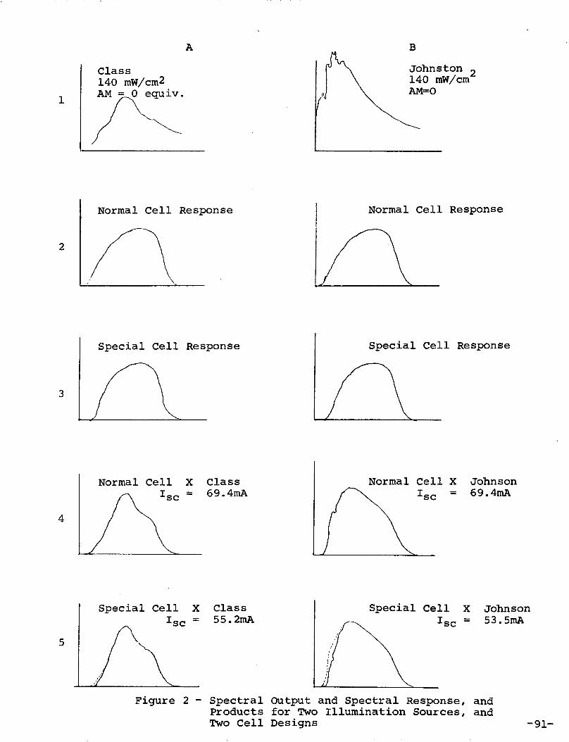
1
A
Class140 mW/cm2
~
Normal Cell Response
B
Johnston 2140 mW/cmAM=O
Normal Cell Response
2
3
Special Cell Response Special Cell Response
4
Normal Cell XI sc =
Class69.4mA
Normal Cell XI sc =
Johnson69.4mA
5
Special Cell XI sc =
Class55.2mA
Special Cell XI sc =
Johnson53.5mA
Figure 2 - Spectral output and Spectral Response, andProducts for Two Illumination Sources, andTwo Cell Designs -91-