Optimization of Nonadsorptive Polymerized Polyethylene ...
130
Brigham Young University Brigham Young University BYU ScholarsArchive BYU ScholarsArchive Theses and Dissertations 2015-03-01 Optimization of Nonadsorptive Polymerized Polyethylene Glycol Optimization of Nonadsorptive Polymerized Polyethylene Glycol Diacrylate as a Material for Microfluidics and Sensor Integration Diacrylate as a Material for Microfluidics and Sensor Integration Chad Rogers Brigham Young University - Provo Follow this and additional works at: https://scholarsarchive.byu.edu/etd Part of the Chemistry Commons BYU ScholarsArchive Citation BYU ScholarsArchive Citation Rogers, Chad, "Optimization of Nonadsorptive Polymerized Polyethylene Glycol Diacrylate as a Material for Microfluidics and Sensor Integration" (2015). Theses and Dissertations. 5310. https://scholarsarchive.byu.edu/etd/5310 This Dissertation is brought to you for free and open access by BYU ScholarsArchive. It has been accepted for inclusion in Theses and Dissertations by an authorized administrator of BYU ScholarsArchive. For more information, please contact [email protected], [email protected].
Transcript of Optimization of Nonadsorptive Polymerized Polyethylene ...
Brigham Young University Brigham Young University
BYU ScholarsArchive BYU ScholarsArchive
Theses and Dissertations
2015-03-01
Optimization of Nonadsorptive Polymerized Polyethylene Glycol Optimization of Nonadsorptive Polymerized Polyethylene Glycol
Diacrylate as a Material for Microfluidics and Sensor Integration Diacrylate as a Material for Microfluidics and Sensor Integration
Chad Rogers Brigham Young University - Provo
Follow this and additional works at: https://scholarsarchive.byu.edu/etd
Part of the Chemistry Commons
BYU ScholarsArchive Citation BYU ScholarsArchive Citation Rogers, Chad, "Optimization of Nonadsorptive Polymerized Polyethylene Glycol Diacrylate as a Material for Microfluidics and Sensor Integration" (2015). Theses and Dissertations. 5310. https://scholarsarchive.byu.edu/etd/5310
This Dissertation is brought to you for free and open access by BYU ScholarsArchive. It has been accepted for inclusion in Theses and Dissertations by an authorized administrator of BYU ScholarsArchive. For more information, please contact [email protected], [email protected].
Optimization of Nonadsorptive Polymerized Polyethylene Glycol Diacrylate as a Material for
Microfluidics and Sensor Integration
Chad Isaac Rogers
A dissertation submitted to the faculty of Brigham Young University
in partial fulfillment of the requirements for the degree of
Doctor of Philosophy
Adam T. Woolley, Chair Gregory P. Nordin
Milton L. Lee Steven R. Goates Daniel E. Austin
Department of Chemistry and Biochemistry
Brigham Young University
February 2015
Copyright © 2015 Chad I. Rogers
All Rights Reserved
ABSTRACT
Optimization of Nonadsorptive Polymerized Polyethylene Glycol Diacrylate as a Material for Microfluidics and Sensor Integration
Chad I. Rogers Department of Chemistry and Biochemistry, BYU
Doctor of Philosophy
Microfluidics is a continually growing field covering a wide range of applications, such as cellular analysis, biomarker quantification, and drug discovery; but in spite of this, the field of microfluidics remains predominately academic. New materials are pivotal in providing tailored properties to improve device integration and decrease prototype turnaround times. In biosensing, nonspecific adsorption in microfluidic systems can deplete target molecules in solution and prevent analytes, especially those at low concentrations, from reaching the detector. Polyethylene glycol diacrylate (PEGDA) mixed with photoinitiator forms, on exposure to ultraviolet (UV) radiation, a polymer with inherent resistance to nonspecific adsorption. Optimization of the polymerized PEGDA (poly-PEGDA) formula imbues this material with some of the same properties, including optical clarity, water stability, and low background fluorescence, that makes polydimethylsiloxane (PDMS) a widely used material for microfluidics. Poly-PEGDA demonstrates less nonspecific adsorption than PDMS over a range of concentrations of flowing fluorescently tagged bovine serum albumin solutions, and poly-PEGDA has greater resistance to permeation by small hydrophobic molecules than PDMS. Poly-PEGDA also exhibits long-term (hour scale) resistance to nonspecific adsorption compared to PDMS when exposed to a low (1 μg/mL) concentration of a model adsorptive protein. Electrophoretic separations of amino acids and proteins resulted in symmetrical peaks and theoretical plate counts as high as 4 × 10⁵/m.
Pneumatically actuated, non-elastomeric membrane valves fabricated from poly-PEGDA have been characterized for temporal response, valve closure, and long-term durability. A ∼100 ms valve opening time and a ∼20 ms closure time offer valve operation as fast as 8 Hz with potential for further improvement. Comparison of circular and rectangular valve geometries indicates that the surface area for membrane interaction in the valve region is important for valve performance. After initial fabrication, the fluid pressure required to open a closed circular valve is ∼50 kPa higher than the control pressure holding the valve closed. However, after ∼1000 actuations to reconfigure polymer chains and increase elasticity in the membrane, the fluid pressure required to open a valve becomes the same as the control pressure holding the valve closed. After these initial conditioning actuations, poly-PEGDA valves show considerable robustness with no change in effective operation after 115,000 actuations.
Often, localized areas of surface functionalization are desired in biosensing, necessitating site-specific derivatization. Integration of poly-PEGDA with different substrates, such as glass,
silicon, or electrode-patterned materials, allows for broad application in biosensing and microfluidic devices. Deposition of 3-(trimethoxysilyl) propyl methacrylate or (3-acryloxypropyl) dimethylmethoxysilane onto these substrates makes bonding to poly-PEGDA possible under UV exposure. Primary deposition of (3-acryloxypropyl) dimethylmethoxysilane, followed by photolithographic patterning, allows for silane removal through HF surface etching in the exposed areas and subsequent deposition of 3-aminopropyldiisopropylethoxysilane on the etched regions. Fluorescent probes are used to evaluate surface attachment methods. Primary attachment via reaction of Alexa Fluor 488 TFP ester to the patterned aminosilane demonstrates excellent fluorescent signal. Initial results with glutaraldehyde were demonstrated but require more optimization before this method for secondary attachment is viable.
Fabrication of 3D printed microfluidic devices with integrated membrane-based valves is performed with a low-cost, commercially available stereolithographic 3D printer and a custom PEGDA resin formulation tailored for low non-specific protein adsorption. Horizontal microfluidic channels with designed rectangular cross sectional dimensions as small as 350 µm wide and 250 µm tall are printed with 100% yield, as are cylindrical vertical microfluidic channels with 350 µm designed (210 µm actual) diameters. Valves are fabricated with a membrane consisting of a single build layer. The fluid pressure required to open a closed valve is the same as the control pressure holding the valve closed. 3D printed valves are successfully demonstrated for up to 800 actuations.
Poly-PEGDA is a versatile material for microfluidic applications ranging from electrophoretic separations, valve implementation, and heterogeneous material integration. Further improvements in PEGDA resin formulation, in combination with a UV source 3D printer, will provide poly-PEGDA devices that are not only rapidly fabricated (<40 min per device), but that also include pumps and valves and are usable with a variety of detection methods, such as laser-induced fluorescence and immunoassays, for broad application in biosensing.
Keywords: Poly-PEGDA, Non-adsorptive polymer, Membrane valve, Valve characterization, 3D printed valve, Microchip electrophoresis, Bioanalytical

ACKNOWLEDGEMENTS
First and foremost, I would like to thank my wife and family for supporting me during
this adventure. Without you I would not be who I am today. I am grateful for my advisor, Dr.
Adam Woolley. Thanks for the gentle guidance and mentorship you have provided. I would also
like to thank Dr. Greg Nordin for our collaboration. It has been enlightening and an honor. To
my other committee members, Dr. Milton Lee, Dr. Steven Goates, and Dr. Daniel Austin, thank
you for your assistance. Your guidance and thought provoking questions have helped shape me
personally as well as my research. All five of you are wonderful mentors and great teachers.
To both previous and current group members of the ATW and Nordin labs, Thank You!
It has been a pleasure to have you as my friends and comrades-in-arms. There are many of you,
too many to list here, but particular thanks go out to Jayson Pagaduan, Mukul Sonker, Suresh
Kumar, Dr. Vishal Sahore, Dr. Ryan Anderson, Dr. Stan Ness, Joseph Oxborrow, Ben Tsai,
Kamran Qaderi, and Hua Gong. Thank you my friends. May your endeavors be blessed!
To my longtime friends, Dr. Dave Jensen and Dr. Landon Wiest, I have only one thing to
say, Δ! It has been a long journey and now a new one begins!

TABLE OF CONTENTS
LIST OF TABLES ......................................................................................................................... ix
LIST OF FIGURES .........................................................................................................................x
1. BACKGROUND AND INTRODUCTION ................................................................................1
1.1. INTRODUCTION ................................................................................................................1
1.2. MATERIALS FOR MICROFLUIDICS ..............................................................................6 1.2.1 Inorganic Materials .......................................................................................................6 1.2.2 Polymers .......................................................................................................................7
1.2.2.1 Elastomers ............................................................................................................ 8 1.2.2.2 Thermoplastics ..................................................................................................... 9
1.2.3 Paper ...........................................................................................................................12 1.2.4 Opportunities for Future Development ......................................................................12
1.3 FUNCTIONS IN LAB-ON-A-CHIP SYSTEMS................................................................13 1.3.1 Sample Preparation .....................................................................................................13
1.3.1.1 Extraction and Purification ................................................................................ 13 1.3.1.2 Preconcentration ................................................................................................ 13 1.3.1.3 On-chip Labeling ............................................................................................... 14
1.3.2 Separation Methods ....................................................................................................15 1.3.2.1 Electrophoresis ................................................................................................... 15
1.3.3 Sensing and Detection ................................................................................................16 1.3.3.1 Optical Detection ............................................................................................... 16 1.3.3.2 Biosensors .......................................................................................................... 19
1.3.4 Fluid Manipulation .....................................................................................................19 1.3.4.1 Pumps ................................................................................................................. 19 1.3.4.2 Valves ................................................................................................................ 21
1.4 DISSERTATION OVERVIEW ..........................................................................................23
1.5 REFERENCES ....................................................................................................................26
2. SINGLE-MONOMER FORMULATION OF POLYMERIZED POLYETHYLENE GLYCOL DIACRYLATE AS A NONADSORPTIVE MATERIAL FOR MICROFLUIDICS ..31
2.1 INTRODUCTION ...............................................................................................................31
v
2.2 EXPERIMENTAL ..............................................................................................................34 2.2.1 Materials .....................................................................................................................34 2.2.2 PDMS Fabrication Summary .....................................................................................35 2.2.3 Poly-PEGDA Fabrication Summary ..........................................................................36 2.2.4 Formula Optimization ................................................................................................38 2.2.5 Burst Pressure Testing ................................................................................................39 2.2.6 Bulk Fluorescence Comparison ..................................................................................41 2.2.7 Rhodamine B Comparison .........................................................................................41 2.2.8 Fluorescence Comparison ..........................................................................................41 2.2.9 Time Comparison .......................................................................................................42 2.2.10 Microchip Electrophoresis .......................................................................................43
2.3 RESULTS AND DISCUSSION .........................................................................................44 2.3.1 Formula Optimization ................................................................................................44 2.3.2 Burst Pressure Tests ...................................................................................................47 2.3.3 Bulk Fluorescence Comparison ..................................................................................48 2.3.4 Rhodamine B Comparison .........................................................................................48 2.3.5 Fluorescence Comparison ..........................................................................................49 2.3.6 Time Comparison .......................................................................................................51 2.3.7 Microchip Electrophoresis .........................................................................................53
2.4 CONCLUSIONS .................................................................................................................54
2.5 REFERENCES ....................................................................................................................55
3. MICROFLUIDIC VALVES MADE FROM POLYMERIZED POLYETHYLENE GLYCOL DIACRYLATE .............................................................................................................57
3.1 INTRODUCTION ...............................................................................................................57
3.2 MATERIALS AND METHODS ........................................................................................60 3.2.1 Reagents and Materials ..............................................................................................60 3.2.2 Device Fabrication .....................................................................................................60 3.2.3 Device Characterization Setup ...................................................................................64
3.3 RESULTS AND DISCUSSION .........................................................................................66 3.3.1 Device Characterization Results ................................................................................66 3.3.2 Device Prospects ........................................................................................................73
3.4 CONCLUSIONS .................................................................................................................74
3.5 REFERENCES ....................................................................................................................75
vi
4. PATTERNED DUAL-SILANE DEPOSITION ON QUARTZ TO ENABLE HYBRID MATERIAL INTEGRATION AND SITE-SPECIFIC FUNCTIONALIZATION ......................78
4.1 INTRODUCTION ...............................................................................................................78
4.2 MATERIALS AND METHODS ........................................................................................79 4.2.1 Reagents and Materials ..............................................................................................79 4.2.2 Device Fabrication .....................................................................................................80 4.2.3 Burst Pressure Evaluation Setup ................................................................................80 4.2.4 Primary Attachment Evaluation .................................................................................81 4.2.5 Secondary Attachment Evaluation .............................................................................82
4.3 RESULTS AND DISCUSSION .........................................................................................83 4.3.1 Burst Pressure Results ................................................................................................83 4.3.2 Primary Attachment Results .......................................................................................85 4.3.3 Secondary Attachment Results ...................................................................................87
4.4 CONCLUSIONS .................................................................................................................89
4.5 REFERENCES ....................................................................................................................89
5. 3D PRINTED MICROFLUIDIC DEVICES WITH INTEGRATED VALVES ......................91
5.1 INTRODUCTION ...............................................................................................................91
5.2 EXPERIMENTAL METHODS ..........................................................................................95 5.2.1 Materials and Methods ...............................................................................................95 5.2.2 Experimental Setup ....................................................................................................96 5.2.3 Membrane Thickness .................................................................................................98 5.2.4 Valve Evaluation and Performance ............................................................................99
5.3 RESULTS AND DISCUSSION .........................................................................................99 5.3.1 Device Characterization Results ................................................................................99 5.3.2 Membrane Thickness ...............................................................................................102 5.3.3 Valve Evaluation and Performance ..........................................................................103
5.4 CONCLUSIONS ...............................................................................................................105
5.5 REFERENCES ..................................................................................................................106
6. CONCLUSIONS AND FUTURE WORK ..............................................................................109
6.1 CONCLUSIONS ...............................................................................................................109
vii

6.1.1 Single-Monomer Formulation of Polymerized Polyethylene Glycol Diacrylate as a Nonadsorptive Material for Microfluidics ......................................................................109 6.1.2 Microfluidic Valves Made from Polymerized Polyethylene Glycol Diacrylate ......109 6.1.3 Patterned Dual-Silane Deposition on Quartz to Enable Hybrid Material Integration and Site-Specific Functionalization ................................................................110 6.1.4 3D Printed Microfluidic Devices with Integrated Valves ........................................111
6.2 FUTURE WORK ..............................................................................................................111 6.2.1 Evaluation of Pumps and Passive Channel Components Made from Poly-PEGDA ..............................................................................................................................111 6.2.2 Optimization of Surface Chemistry Attachment ......................................................113 6.2.3 Reformulation of 3D Printing Poly-PEGDA Resin for Better Resolution, Decreased Coloration, and Reduced Background Fluorescence .......................................113
6.3 REFERENCES ..................................................................................................................117
viii
LIST OF TABLES
Table 2.1. Formulas for PEG Optimization for Water Stability. .................................................. 39
Table 2.2. Results for PEG Optimization for Water Stability with 10 s Exposure Time. ............ 46
Table 2.3. Results for PEG Optimization for Water Stability with 25 s Exposure Time. ............ 47
Table 3.1. Summary of Results for Each Valve Geometry........................................................... 69
Table 3.2. Data for Young’s Modulus Calculations in Equation 3.1. ........................................... 71
ix
LIST OF FIGURES
Figure 1.1. Schematic of common microfluidic components in an integrated device,
demonstrating different components such as fluid manipulation (channels, valves, and pumps),
sample preparation (purification, labeling, etc.), separation mechanism, and detection scheme. ...4
Figure 1.2. Overview of electroosmotic flow (EOF) and flow profile comparison. .......................5
Figure 1.3. On-chip labeling overview. .........................................................................................14
Figure 1.4. Overview of “pinched” injection and separation in µCE. ...........................................17
Figure 1.5. Overview of LIF setup.................................................................................................18
Figure 1.6. Overview of passive and active valves. .......................................................................22
Figure 2.1. Poly-PEGDA flow channel device used to evaluate nonspecific adsorption. .............37
Figure 2.2. Polymerization of PEGDA to form poly-PEGDA. .....................................................38
Figure 2.3. Burst pressure testing of bond strength between poly-PEGDA layers........................40
Figure 2.4. SEM images of poly-PEGDA channels. .....................................................................45
Figure 2.5. Transmission spectra of 200-µm-thick layers of PDMS and poly-PEGDA. ..............45
Figure 2.6. Mechanical flexibility. .................................................................................................46
Figure 2.7. Plot of fluorescence signal cross sections at different times during flow of 10 µM
rhodamine B at 0.2 µL/min in 50 µm wide channels in poly-PEGDA and plasma-bonded
PDMS. ............................................................................................................................................49
Figure 2.8. Background-subtracted fluorescence signal in PDMS and poly-PEGDA
microdevices for increasing FITC-BSA concentrations. ...............................................................51
Figure 2.9. Fluorescence comparison of PDMS and poly-PEGDA over time during flow of a
dilute FITC-BSA solution. .............................................................................................................52
x
Figure 2.10. Electrophoretic separation of amino acids and proteins using a poly-PEGDA
microchip. ......................................................................................................................................53
Figure 3.1. Schematic of a three-layer poly-PEGDA valve...........................................................58
Figure 3.2. Overview of poly-PEGDA valve fabrication. .............................................................62
Figure 3.3. Vacuum clamp for bonding. ........................................................................................63
Figure 3.4. Images of the experimental setup. ...............................................................................64
Figure 3.5. Photomicrograph of a rectangular valve with a 15 µm pedestal width, a 600 x 640
µm2 control layer, a 550 x 600 µm2 fluid channel in the valve region, and a 100 µm wide fluid
channel leading into and out from the valve. .................................................................................67
Figure 3.6. Valve temporal response. ............................................................................................68
Figure 3.7. Fluid pressure and volumetric flow rate as a function of time for a constant control
pressure. .........................................................................................................................................69
Figure 3.8. Calculated (line) and experimentally measured (circles) deflection via applied
pressure, for a 45 µm thick circular membrane with an elastic modulus of 0.13 GPa, a 350 µm
radius, and a Poisson’s ratio of 0.35. .............................................................................................70
Figure 3.9. Valve performance after a number of actuations as a function of control pressure. ...72
Figure 4.1. Dual silane deposition overview. ................................................................................82
Figure 4.2. Photograph of poly-PEGDA device bonded to quartz. ...............................................83
Figure 4.3. Burst pressure results for silane functionalized silicon bound to poly-PEGDA. ........84
Figure 4.4. Burst pressure result for poly-PEGDA bound to trifunctional TMSPMA
functionalized quartz. .....................................................................................................................85
Figure 4.5. Fluorescent image of a device demonstrating the importance of removing all the
photoresist after APDIES deposition.. ...........................................................................................86
xi
Figure 4.6. Fluorescence comparison (A) before and (B) after Alexa Fluor 488 attachment. ......87
Figure 4.7. Secondary attachment of a fluorescent probe utilizing glutaraldehyde as a cross-
linker. .............................................................................................................................................88
Figure 5.1. Valve schematic and device image.. ............................................................................96
Figure 5.2. Fabrication process. .....................................................................................................98
Figure 5.3. Horizontal channel fabrication, repeatability, and yield. ..........................................101
Figure 5.4. Vertical cylindrical channel fabrication, repeatability, and yield. .............................102
Figure 5.5. Measured membrane thickness as a function of layer exposure time. ......................103
Figure 5.6. Valve operation and evaluation. ................................................................................104
Figure 6.1. Poly-PEGDA device with integrated pumps and valves, for solid-phase extraction
and electrophoretic separation. ....................................................................................................112
Figure 6.2. Schematic of a pump network utilizing a centralized larger valve to push fluid
through the system. ......................................................................................................................115
Figure 6.3. Schematic of a 3-valve peristaltic pump where the middle valve is inverted to
decrease the channel volume in between the valves. ...................................................................115
Figure 6.4. Sample individual passive components in 3D printed microfluidics. .......................116
xii
1. BACKGROUND AND INTRODUCTION*
1.1. INTRODUCTION
Chemical analysis is a crucial part of science in understanding the world around us. Through
probing a system of interest (e.g., via light, electricity, heat, mass, or mass-to-charge ratio)
valuable information about relative quantities and chemical makeup is gained. For chemical
analysis to work, energy added to the system must induce a change and be coupled with a way to
detect that change.1 Although a variety of ways have been developed to do this, the field of
microfluidics, also known as lab-on-a-chip or micro total analysis systems (µTAS), will be the
focus of this dissertation. The premise of lab-on-a-chip systems is taking larger, bulky analysis
systems and shrinking them down so that a similar process can be done on a small chip. This
results in reduced solvent and sample volumes, greater portability (as long as the supporting
equipment is similarly shrunk down), and the ability to integrate multiple processes into one
device. Due to smaller required sample volumes, one focus of microfluidics has been
biochemical analysis, where only small sample amounts are available for testing (e.g.,
cerebrospinal fluid or antibodies, the latter due to cost).
Microfabricated structures between 1–500 µm for manipulation and handling of small liquid
volumes (femtoliters to nanoliters) create the bulk of microfluidics. Although they utilize small
volumes, capillary tubes connected with capillary fittings,2 and millifluidics made by machine
shop tools are not included in microfluidics in this chapter since they are not microfabricated and
have larger channel dimensions (>500 µm).
*Sections 1.1˗1.3 are adapted with permission from Chemical Reviews, Nge, P. N.; Rogers, C. I.; Woolley, A. T., Chem. Rev. 2013, 113 (4), 2550-2583. Copyright 2013 American Chemical Society.
1

Though microfluidics has been around since the 1970s,3 the field did not gain much traction in
academia until the 1990s.4 Silicon and glass were the original materials used, but in the 1990s
focus shifted to include polymer substrates, in particular, polydimethylsiloxane (PDMS). Since
then the field has grown to include a wide variety of materials and applications. The successful
demonstration and integration of electrophoresis in a microfluidic device provided a
nonmechanical method for both fluid control and separation.5 Laser induced fluorescence (LIF)
provided for sensitive detection of fluorophores or fluorescently labeled molecules. The advent
of high-resolution printing allowed for more rapid and cheaper mask fabrication for use in soft
lithography.6 A number of companies, including Abbott, Agilent, Caliper, Dolomite, Micralyne,
Microfluidic Chip Shop, Micrux Technologies and Waters, have now developed microfluidic
devices that are commercially available. For a more thorough review of the history of
microfluidics, I refer you to reviews by Manz et al.4, 7-11 or Whitesides et al.12
Microfluidics has many advantages compared to standard large scale systems. The first relates to
a lesson taught to every first-year chemistry student. Simply stated, diffusion is slow! The
equation for one dimensional diffusion is given by Eq. 1.1
𝑥𝑥 = √4𝐷𝐷𝐷𝐷 (1.1)
where x is distance, D is the diffusion coefficient, and t the time.13 Rearranging this equation for t
gives Eq. 1.2.
𝐷𝐷 = 𝑥𝑥2
4𝐷𝐷 (1.2)
For a common protein, bovine serum albumin (BSA, D = 6 x 10⁻⁷ cm2/s),14 the time required to
travel 1 mm is ~69 min. The smaller the distance required for interaction, the smaller the time
needed for interaction (the diffusion time for BSA to travel 100 µm is ~42 s). Smaller channel
2
dimensions also can lead to smaller sample volumes (fL-nL) which can reduce the amount of
sample and reagents required for testing and analysis. Reduced dimensions can also lead to more
portable devices that can enable on-site testing (as long as the equipment to analyze the device
and sample are similarly portable). Integration of different processes (like labeling, purification,
separation, and detection) in a microfluidic device can contribute to broader applications.
Chip integration leads to a more complete analytical package. Microelectromechanical systems
(MEMS) are small devices composed of electrical and mechanical parts to create an integrated
sensor or system. Applications of MEMS devices are found in a range of areas including
automobiles, phones, video games, and medical and biological sensors.15 Lab-on-a-chip or µTAS
are integrated microfluidic devices that are capable of multiple steps that can ideally provide
minimal user involvement to sense molecules of interest. For example, a lab-on-a-chip system
might selectively purify a complex mixture (through filtering, antibody immobilization, etc.),
separate analytes, and detect those analytes.
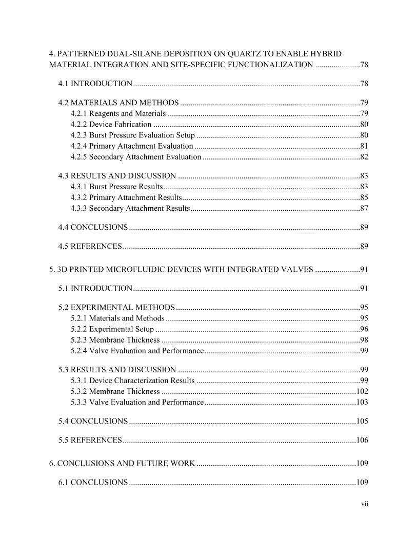
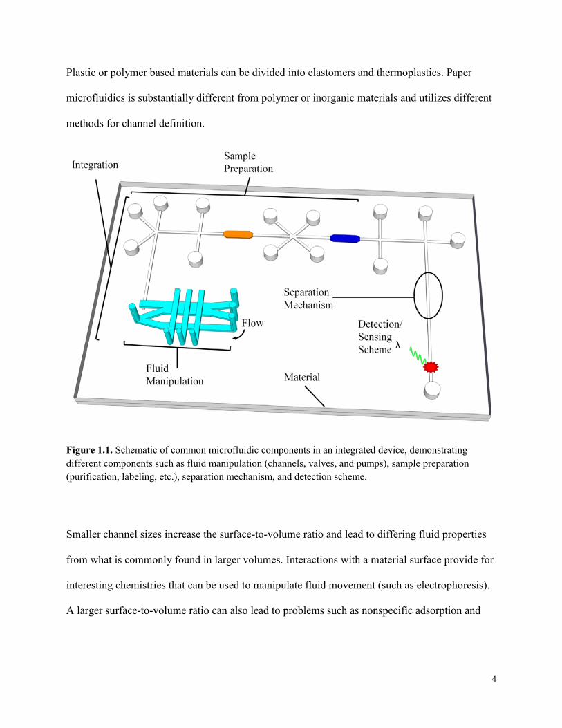
Microfluidic devices consist of several similar components (Fig. 1.1). Negative features such as
reservoirs (wells) and microchannels provide the standard starting point for most microfluidic
devices. Positive features add increased functionality to the chip and can consist of membranes,
monoliths, pneumatic controls and valves, and beams and pillars.
Initially, microfluidic materials consisted of silicon and glass substrates. As focus into
microfluidics increased, other materials (e.g., polymers, ceramics, and paper) were characterized
for utilization in microfluidics. These materials can be organized into three broad material
categories: inorganic, polymeric, and paper. Inorganic materials have broadened beyond glass
and silicon to include ceramics such as low temperature co-fired ceramics and vitoceramics.
3
Plastic or polymer based materials can be divided into elastomers and thermoplastics. Paper
microfluidics is substantially different from polymer or inorganic materials and utilizes different
methods for channel definition.
Figure 1.1. Schematic of common microfluidic components in an integrated device, demonstrating different components such as fluid manipulation (channels, valves, and pumps), sample preparation (purification, labeling, etc.), separation mechanism, and detection scheme.
Smaller channel sizes increase the surface-to-volume ratio and lead to differing fluid properties
from what is commonly found in larger volumes. Interactions with a material surface provide for
interesting chemistries that can be used to manipulate fluid movement (such as electrophoresis).
A larger surface-to-volume ratio can also lead to problems such as nonspecific adsorption and
4

surface fouling. Flow in these devices is normally nonturbulent due to a low Reynolds number.
Since flow is nonturbulent, mixing is normally diffusion limited.
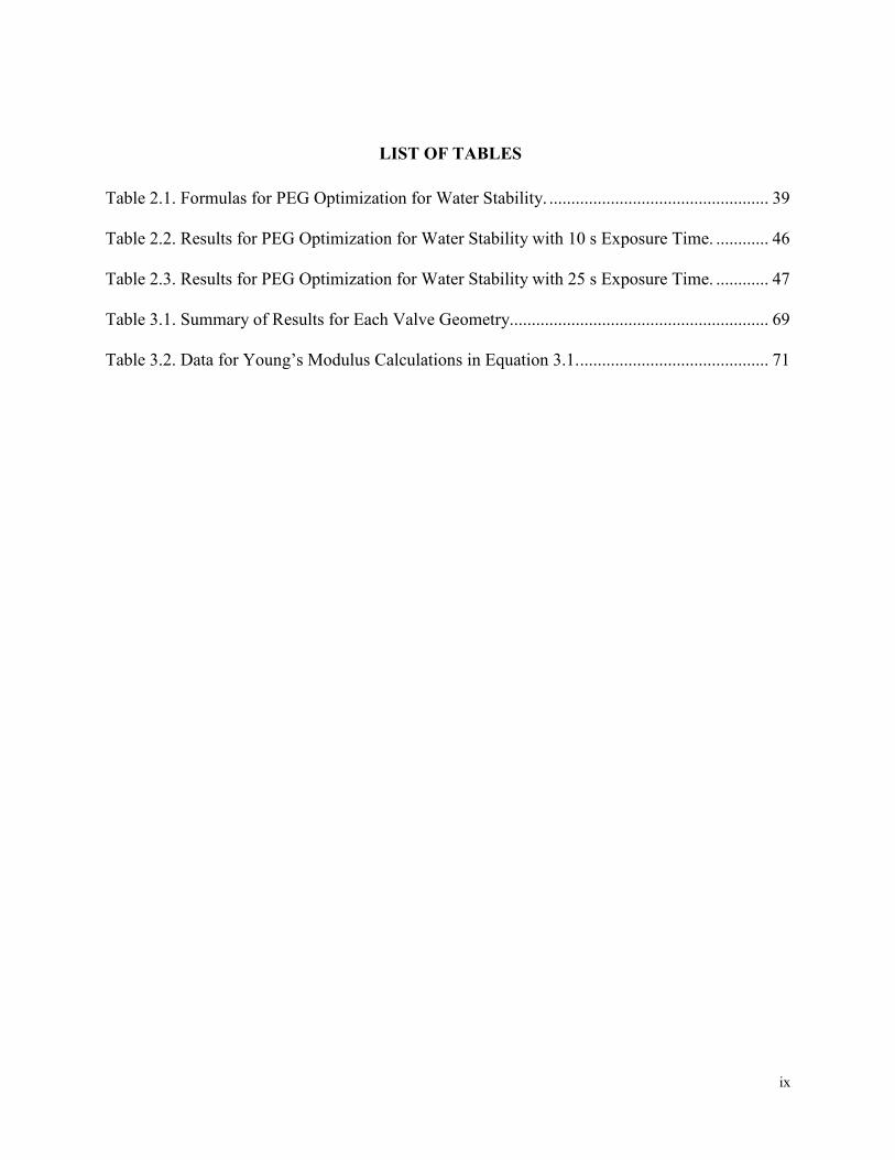
Surface charge on the exposed material surface exerts a greater influence on the fluid in the
channel as channel size decreases. Water, an amphoteric molecule, can be drawn through small
channels through capillary action because of attraction between polar water molecules and partial
or full charges present on the channel surface. In the presence of a salt solution, this interaction
creates an electrical double layer of charge (Fig. 1.2) as buffer ions interact with surface charge.
This double layer is the basis for electroosmosis as an applied voltage causes the loosely bound
secondary layer to move towards an electrode and drag the bulk channel solution along with it to
create electroosmotic flow. Hydrophobic channel surfaces are harder to fill with aqueous
solutions (only van der Waals interactions) and can cause proteins in solution to denature and
stick to the channel surface.
Figure 1.2. Overview of electroosmotic flow (EOF) and flow profile comparison. (Left) Ions concentrated at the surface create an electrical double layer which consists of two parts: a tightly bound rigid layer and loosely bound diffuse layer. Applied voltage causes the diffuse layer to move, pulling the bulk solution along with it, creating flow. (Right) Flow profile differs based on driving mechanism: EOF is relatively flat, laminar flow is parabolic, and turbulent flow is flattened in comparison to laminar flow.
5
This chapter will discuss properties and applications of commonly used materials followed by a
brief overview of lab-on-a-chip functions. Finally, a summary of my research on the
development of polymerized polyethylene glycol diacrylate as a microfluidic substrate will be
given.
1.2. MATERIALS FOR MICROFLUIDICS
There are three main factors to choosing a design or material to use in a microfluidic system:
required function, degree of integration, and application. Closely related, these three factors
require consideration of material properties and fabrication processes. Flexibility, air
permeability, nonspecific adsorption, cellular compatibility, solvent compatibility, and optical
transmission are all physical characteristics that must be considered when choosing a material.
Integration of fluid movement and control, detection mechanism, and chip automation can
introduce a higher level of complexity in the fabrication process. The most important question,
however, is what are you trying to accomplish with this device? Aqueous solutions are
compatible with a broad range of materials, and limiting choices could be more of personal
preference. Many organic solutions cause polymer substrates to swell and crack, or dissolve.
Paper microfluidic devices are limited to capillary action as fluid wicks through the paper.
Active components made from glass and silicon are more difficult to fabricate and fragile.
Interfacing these materials with a more flexible material such as PDMS can enable integration of
pneumatic pumps and valves.16, 17 These characterizations are only a few of the considerations
needing to be made when choosing a material for an application.
1.2.1 Inorganic Materials
Silicon was the first material used for microfluidics,3 but current focus is on hybrid devices
(glass or polymer bonded to silicon).18, 19 Silicon is transparent to infrared wavelengths but not
6
ultraviolet-visible wavelengths, making fluorescence detection or debugging impossible in this
range for an embedded channel in silicon. This is overcome by having a UV-VIS transparent
material (polymer or glass) bound to silicon. Silicon chemistry focuses on the silanol group (–Si-
OH) and is well-developed so surface modification is easily accomplished. Silicon has a high
elastic modulus (130-180 GPa) and is not easily made into active fluidic components.
Applications of silicon microfabricated devices have ranged from PCR20 and nanowires21 to
cellular culture.22 Nonspecific adsorption can be reduced and cellular growth improved through
chemical modification of the surface.23, 24 Fabrication for silicon (and consequently glass
devices) utilizes either subtractive methods (chemical wet or dry etching) or additive methods,
such as metal or chemical deposition, to create channels.25
Glass has low background fluorescence and like silicon, modification chemistries are silanol
based. Since glass has a large elastic modulus (varies by composition), hybrid devices are
required for active components such as valves and pumps.16, 17 It is possible to deposit electrodes
onto glass but the raised area of the electrodes creates problems when trying to bond to a glass
top-layer. Glass is compatible with biological samples, has relatively low nonspecific adsorption,
and is not gas permeable. Microfluidic channels are created by etching into the glass through wet
or dry etch methods.25 Applications focus on both all-glass and hybrid microchips.
1.2.2 Polymers
Polymers are organic-based, long-chain materials that have gained significant traction in
microfluidics in the past 15 years. Polymers are advantageous for microfluidic device fabrication
because they are relatively inexpensive, amenable to mass production processes (e.g., hot
embossing, injection molding, etc.), and adaptable through formulation changes and chemical
modification.
7
1.2.2.1 Elastomers
PDMS was first introduced as a microfluidic substrate in the late 1990s.26, 27 Now it is one of the
most common microfluidic substrates in use due to its rapid fabrication time, good bond strength,
and ease of implementation. Device molds are formed utilizing soft lithography methods and
multiple layers can be used to create complex fluidic designs.28 Low elastic modulus (300-500
kPa) makes PDMS popular for use in valves and pumps.29-31 PDMS is gas permeable, but low-
molecular-weight oligomers in the polymer can drift to the surface causing hydrophobic recovery
after plasma exposure.32 Oligomers can also leach out into the sample solution, negatively
impacting cellular studies, for example.33 A hydrophobic material, PDMS is susceptible to
nonspecific adsorption and permeation by hydrophobic molecules.34 Chemical modification is
needed to correct for these shortcomings. Plasma exposure will hydrophilize the exposed
polymer surface, but only for a short time.32, 35 Silanol reaction usually follows plasma activation
to prevent this change in surface properties.36, 37
The inertness of perfluorinated compounds (e.g., Teflon-coated cookware) makes this class of
materials attractive for microfluidics; such surfaces are both oleophobic and hydrophobic.
Although there are several formula variations, most fluoroelastomers are perfluoropolyethers
(PFPE), sometimes described as “liquid Teflon”. Rolland et al.38 demonstrated that PFPE diol
methacrylate (DMA) could be utilized to make valves similar to ones in PDMS. PFPE DMA
showed reduced swelling in the presence of organic solvents compared to PDMS and had a
Young’s modulus of 3.9 MPa. Rolland et al.39 further demonstrated that PFPE-DMA could form
sub-micron resolution molds down to 50 nm. De Marco et al.40 showed that UV-cured PFPE
could be bound to PDMS and determined a 1.52 MPa delamination pressure between bonded
8
PFPE layers. Since fluorinated surfaces are both hydrophobic and oleophobic, bonding to glass
and similar substrates tends to be very weak.41
1.2.2.2 Thermoplastics
Thermoplastics are densely crosslinked polymers that are moldable when heated to their glass
transition temperature but retain their shape when cooled. These materials are generally durable,
amenable to micromachining processes, optically clear, resistant to permeation of small
molecules and stiffer than elastomers. Thermoplastics require pedestal-valve geometries16 for
valves since the material is unable to collapse on itself to form a seal. Thermoplastic raw
materials are available commercially through companies such as Topas, Zeonex, Aline
Components and Optical Polymers Lab Corp.
Polystyrene (PS) is preferred by biologists over PDMS for cell culture, and most focus in
microfluidics for this material is on cell culture and analysis.33 PS microdevices are formed by
melting polymer beads onto a mold to form channels.42 PS having predominately styrene on the
surface requires plasma oxidation or chemical modification to make PS hydrophilic.42, 43
Adaptation of “Shrinky Dinks”, a childrens’ toy made from PS, resulted in well-sealed devices
and higher channel aspect ratios due to polymer shrinkage.44 Young et al.43 optimized, using an
epoxy mold, the formation of PS channels by hot embossing to create a more rapid fabrication
process. Subsequent thermal bonding resulted in very strong adhesion between two PS layers.
Polycarbonate (PC) is a durable material created by polymerization of bisphenol A and
phosgene, resulting in repeating carbonate groups. Predominately used for DNA analysis due to
its high softening temperature (~145°C), PC channels are fabricated by hot embossing a silicon
9
mold into a thin layer of PC and subsequently laminating two layers together using thermal
bonding.45, 46 PC has an elastic modulus of 2.3-2.4 GPa.47
Poly(methyl methacrylate) (PMMA), formed through the polymerization of methyl methacrylate,
is widely known under the commercial names of Plexiglas and Lucite. PMMA has an elastic
modulus of 3.3 GPa and good optical clarity.48 Channels are formed in PMMA through hot
embossing.49 Several different methods for bonding have been demonstrated to avoid collapsed
channels.50 Brown et al.51 evaluated bonding strength with different chemical surface
modifications. Yang et al.52 demonstrated separation of α-fetoprotein (AFP) from blood serum
using immunoaffinity extraction followed by electrophoretic separation and compared results to
ELISA. Yang et al.53 further demonstrated that multiple proteins could be selectively extracted
from human serum and then quantified in a multiplexed device.
Chemical modification of acrylic polymers through direct incorporation of polyethylene glycol
(PEG) helps to reduce nonspecific adsorption of proteins and cells.54 Kim et al. 54 demonstrated
that channels could be made down to 50 nm using UV exposure to bond PEG diacrylate
(PEGDA) or PEG dimethacrylate (PEGDMA) layers. Kim et al.55 further evaluated formation of
nanochannels and nanostructures over an entire wafer using PEGDA reversibly attached to a
gold or silicon substrate as mold for nanostructures made from a mercapto-ester adhesive,
NOA 71. Plasma oxidized gold was shown to aid in the release of PEGDA from the mold.
Extended UV exposure was used to avoid liquid residue on the PEGDA-silicon interface. Liu et
al.56 (and later Sun et al.57) demonstrated electrophoretic separations of amino acids, peptides and
proteins in a PEG-based copolymer containing PEGDA, PEG methyl ether methacrylate
(PEGMEMA), and methyl methacrylate (MMA). Sun et al.58 showed that this PEG
functionalized copolymer could be used in electric field gradient focusing. Klasner et al.59
10
demonstrated a PDMS-co-poly(ethylene oxide) material which had decreased optical clarity
compared to PDMS but incorporated the non-adsorptive poly(ethylene oxide) moiety directly
within the PDMS without requiring surface modification. Amino acid separations were also
demonstrated within devices made from this polymer.
Cyclic-olefin copolymer (COC) is a commercially available, optically transparent material60 that
is suitable for use with most solvents and aqueous solutions,61, 62 has good moldability, and low
background fluorescence. Steigert et al.63 demonstrated COC device formation through
utilization of an epoxy mold master. The epoxy mold was used to emboss macro and micro
features into the COC through embossing. Roy et al.64 investigated the effect of plasma exposure
on COC using oxygen, argon, and nitrogen. Each treatment was compared for bonding strength
and platelet adhesion. They further determined that nitrogen plasma treatment of COC provided
the best combination of hydrophilicity, EOF strength, and biocompatibility. Since COC is a
hydrophobic polymer, chemical modification is necessary to be able to separate proteins using
COC devices.60 Dynamic coating with 2-hydroxylethyl cellulose reduces nonspecific protein
adsorption noticeably as has been demonstrated by Zhang et al.60
SU8 is an epoxy-based polymer that is most commonly used in microfluidics to form a mold to
create channels in another polymer. Multiple SU8 layers are easily fabricated,65 and high aspect
ratio features are readily made using soft lithography techniques. SU8 is transparent in the
visible spectrum but not the UV and has an orange-brown coloration. SU8 has an elastic modulus
of 2.0 GPa and has been used to create flexible check valves.66 Protein detection was
demonstrated showing low nonspecific adsorption and protein compatibility.67 SU8/Pyrex
devices are now being sold commercially through Micrux Technologies.
11

1.2.3 Paper
Paper is a flexible material predominantly made of cellulose and is beneficial as a microfluidic
substrate for several reasons: (1) paper is cheap and readily available around the world; (2) the
material burns easily and safely and will naturally degrade; (3) inkjet and solid wax printing
enable easy channel or pattern definition and functionalization; (4) its porous structure allows for
a combination of flow, filtering, and separation; (5) paper is biologically compatible; (6) paper
can be chemically modified through composition/formulation changes or through attachment
chemistries; (7) and the normally white background provides great contrast for color-based
detection methods.68, 69 Paper-based microfluidics relies on the passive mechanism of capillary
action to pull solutions through the device. Electrochemical micro-paper-based analytical devices
have been demonstrated to detect glucose, cholesterol, and lactose in blood serum.70
Colorimetric detection was utilized to quantify nitrites in saliva and ketones in urine using a
paper-based microfluidic device.71
1.2.4 Opportunities for Future Development
Numerous materials for microfluidics have been introduced over the past 25 years. Each material
comes with a set of inherent strengths and weaknesses. Many materials (e.g., PDMS) have
remained firmly planted in the academic world but have failed to gain traction commercially.
How can the field break this barrier? The key lies in both the fabrication and evaluation of
materials that are not only readily mass producible and inexpensive, but also an integral part of a
compelling application. Hybrid devices, which reap the benefits of each material’s strengths,
have shown promise in achieving this goal. In biological applications, development of a material
with inherent resistance to nonspecific adsorption is desirable, as long as the material still has
other desirable properties for microfluidic applications (e.g., good optical clarity, water stability,
12
high bond strength, low background fluorescence, resistance to small molecule permeation, and
the ability to create valves and pumps). The ideal material also needs to be capable of short
design and turnaround times for rapid prototyping and integration with different substrates.
1.3 FUNCTIONS IN LAB-ON-A-CHIP SYSTEMS
Microfluidic functions are the basic operations in a microchip system, which combined lead to
the desired analysis capability. Key functions include sample preparation, separation, detection,
and liquid transport. Device functions and the overall objective of the analysis dictate the design
and hardware required for each platform. A brief overview is included here.
1.3.1 Sample Preparation
Though the integration of sample preparation in microfluidics devices can be challenging,
significant progress has been made in this area.72 Advantages include reduction in analysis time
and improved throughput.73
1.3.1.1 Extraction and Purification
Solid-phase extraction (SPE) is a popular preparation method wherein analytes are retained on a
solid support and are subsequently eluted in a concentrated form.74, 75 This method is easily
integrated with other processes like PCR, separation, and detection in a microfluidic platform.76
The most common SPE modes in microfluidics are reversed-phase, for non-polar to moderately
polar compounds, and affinity. Affinity extraction techniques which are based on the strong
affinity between an analyte and a compound bonded to the column are highly specific.
1.3.1.2 Preconcentration
Various on-line sample preconcentration techniques, utilizing analyte characteristics such as
charge, affinity, mobility, and size, have been applied to overcome the low concentration
13
sensitivity resulting from the short optical path lengths in microfluidic channels.77 An additional
benefit of concentrating samples prior to analysis is improved detection of low concentration
analytes typically encountered in real world samples.78
1.3.1.3 On-chip Labeling
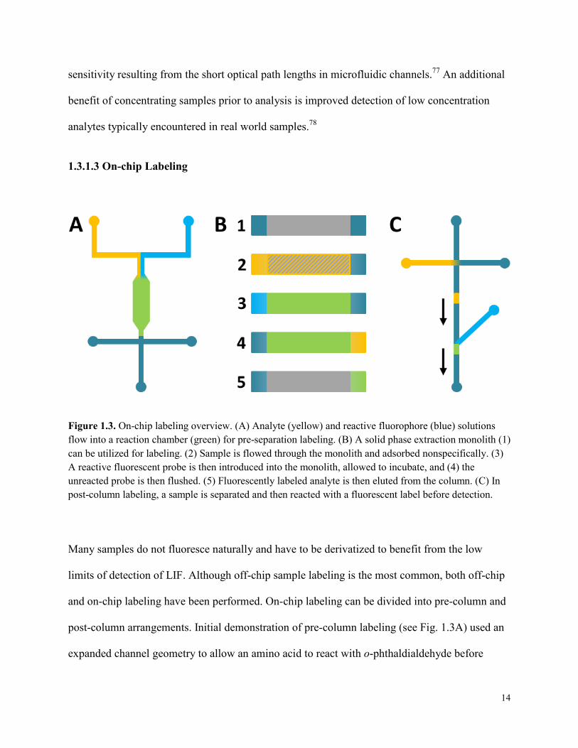
Figure 1.3. On-chip labeling overview. (A) Analyte (yellow) and reactive fluorophore (blue) solutions flow into a reaction chamber (green) for pre-separation labeling. (B) A solid phase extraction monolith (1) can be utilized for labeling. (2) Sample is flowed through the monolith and adsorbed nonspecifically. (3) A reactive fluorescent probe is then introduced into the monolith, allowed to incubate, and (4) the unreacted probe is then flushed. (5) Fluorescently labeled analyte is then eluted from the column. (C) In post-column labeling, a sample is separated and then reacted with a fluorescent label before detection.
Many samples do not fluoresce naturally and have to be derivatized to benefit from the low
limits of detection of LIF. Although off-chip sample labeling is the most common, both off-chip
and on-chip labeling have been performed. On-chip labeling can be divided into pre-column and
post-column arrangements. Initial demonstration of pre-column labeling (see Fig. 1.3A) used an
expanded channel geometry to allow an amino acid to react with o-phthaldialdehyde before
14
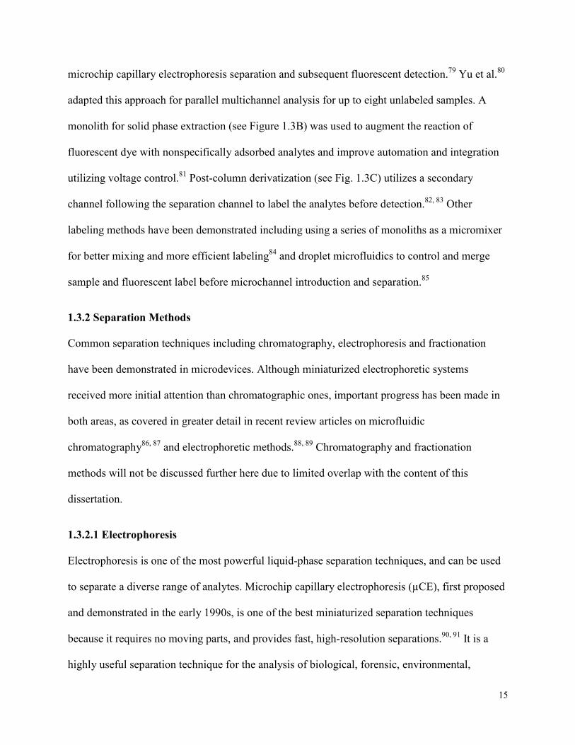
microchip capillary electrophoresis separation and subsequent fluorescent detection.79 Yu et al.80
adapted this approach for parallel multichannel analysis for up to eight unlabeled samples. A
monolith for solid phase extraction (see Figure 1.3B) was used to augment the reaction of
fluorescent dye with nonspecifically adsorbed analytes and improve automation and integration
utilizing voltage control.81 Post-column derivatization (see Fig. 1.3C) utilizes a secondary
channel following the separation channel to label the analytes before detection.82, 83 Other
labeling methods have been demonstrated including using a series of monoliths as a micromixer
for better mixing and more efficient labeling84 and droplet microfluidics to control and merge
sample and fluorescent label before microchannel introduction and separation.85
1.3.2 Separation Methods
Common separation techniques including chromatography, electrophoresis and fractionation
have been demonstrated in microdevices. Although miniaturized electrophoretic systems
received more initial attention than chromatographic ones, important progress has been made in
both areas, as covered in greater detail in recent review articles on microfluidic
chromatography86, 87 and electrophoretic methods.88, 89 Chromatography and fractionation
methods will not be discussed further here due to limited overlap with the content of this
dissertation.
1.3.2.1 Electrophoresis
Electrophoresis is one of the most powerful liquid-phase separation techniques, and can be used
to separate a diverse range of analytes. Microchip capillary electrophoresis (µCE), first proposed
and demonstrated in the early 1990s, is one of the best miniaturized separation techniques
because it requires no moving parts, and provides fast, high-resolution separations.90, 91 It is a
highly useful separation technique for the analysis of biological, forensic, environmental,
15
pharmaceutical, and food samples.92 Unlike in traditional CE instrumentation, which consists of
a single capillary, many different capillaries and fluidic channels can be patterned on a
microfluidic device to improve throughput.91 Advantages of electrophoretic methods include
high efficiency, speed, and low sample consumption.92 Importantly, µCE’s usefulness is
increased by the integration of processes such as PCR, enzymatic digestion, and SPE.91
However, µCE’s applicability is limited because it has lower concentration sensitivities than
liquid chromatography, due to the injection of small volumes in addition to a short optical path
length as a result of the small height of the microchannel.92
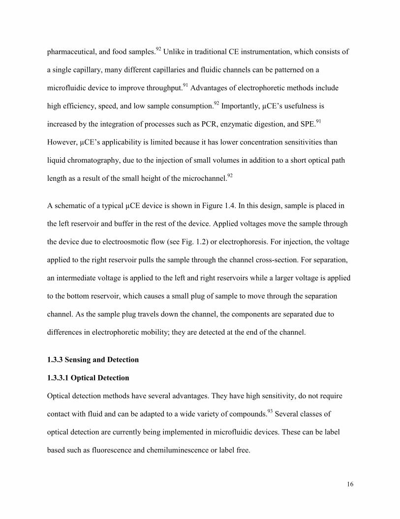
A schematic of a typical µCE device is shown in Figure 1.4. In this design, sample is placed in
the left reservoir and buffer in the rest of the device. Applied voltages move the sample through
the device due to electroosmotic flow (see Fig. 1.2) or electrophoresis. For injection, the voltage
applied to the right reservoir pulls the sample through the channel cross-section. For separation,
an intermediate voltage is applied to the left and right reservoirs while a larger voltage is applied
to the bottom reservoir, which causes a small plug of sample to move through the separation
channel. As the sample plug travels down the channel, the components are separated due to
differences in electrophoretic mobility; they are detected at the end of the channel.
1.3.3 Sensing and Detection
1.3.3.1 Optical Detection
Optical detection methods have several advantages. They have high sensitivity, do not require
contact with fluid and can be adapted to a wide variety of compounds.93 Several classes of
optical detection are currently being implemented in microfluidic devices. These can be label
based such as fluorescence and chemiluminescence or label free.
16

Figure 1.4. Overview of “pinched” injection and separation in µCE. (Left) Injection: voltage is applied in one reservoir to move the sample (red line) through the cross-section. Flow direction is shown by the black arrows. (Right) Separation: components of the sample move down the channel, are separated, and then are detected toward the end of the channel (X).
Laser-induced fluorescence (LIF) is the most widely used optical method in µCE because of its
high sensitivity.94 However, samples that do not fluoresce naturally need to be derivatized, often
with variants of either fluorescein or rhodamine, which fluoresce in the green and red regions of
the spectrum, respectively.94 In most cases the actual optics used for detection in microfluidics
are not integrated in the chip. For LIF detection, a laser is used for excitation, and a
photomultiplier or CCD is used for detection (see Fig. 1.5).95, 96 While label-based methods
require time consuming sample derivatization, their detection limits are typically better than for
label-free methods.
17

Figure 1.5. Overview of LIF setup.
Chemiluminescence detection, which has the advantage of not requiring excitation
instrumentation that produces background interference, but instead requires very sensitive
detectors, has also been demonstrated in both off-chip and on-chip formats. The technique is
based on the production of electromagnetic radiation when the product of a chemical reaction
luminesces or donates its energy to another molecule that luminesces.97 Microchip
electrophoresis and chemiluminescence detection were developed for the determination of
intracellular sulphydryl compounds using the luminol–Na2S2O8 reaction.98
UV absorbance is a label-free detection method commonly used in chromatography and
electrophoresis systems because of its ability to directly detect a wide range of analytes without a
derivatization step. However, in microfluidic systems, the sensitivity is limited by the short
18
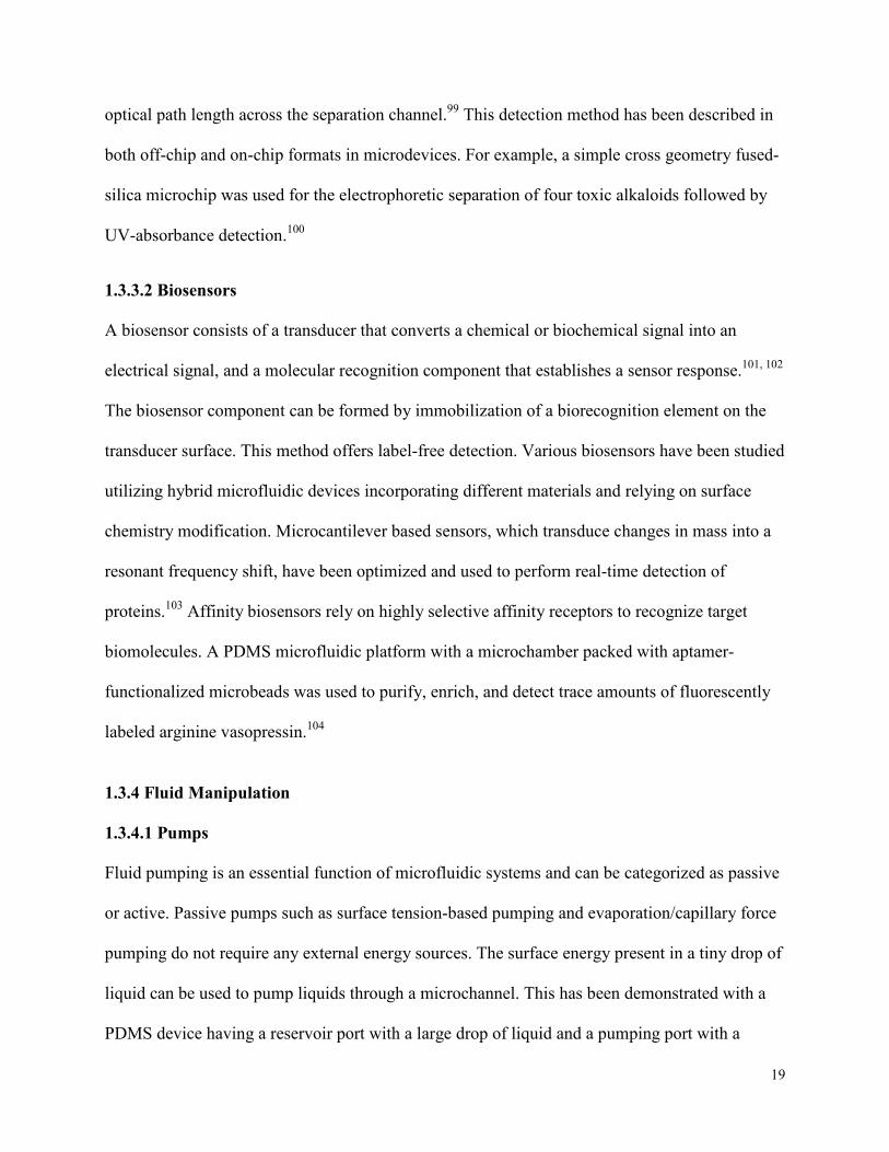
optical path length across the separation channel.99 This detection method has been described in
both off-chip and on-chip formats in microdevices. For example, a simple cross geometry fused-
silica microchip was used for the electrophoretic separation of four toxic alkaloids followed by
UV-absorbance detection.100
1.3.3.2 Biosensors
A biosensor consists of a transducer that converts a chemical or biochemical signal into an
electrical signal, and a molecular recognition component that establishes a sensor response.101, 102
The biosensor component can be formed by immobilization of a biorecognition element on the
transducer surface. This method offers label-free detection. Various biosensors have been studied
utilizing hybrid microfluidic devices incorporating different materials and relying on surface
chemistry modification. Microcantilever based sensors, which transduce changes in mass into a
resonant frequency shift, have been optimized and used to perform real-time detection of
proteins.103 Affinity biosensors rely on highly selective affinity receptors to recognize target
biomolecules. A PDMS microfluidic platform with a microchamber packed with aptamer-
functionalized microbeads was used to purify, enrich, and detect trace amounts of fluorescently
labeled arginine vasopressin.104
1.3.4 Fluid Manipulation
1.3.4.1 Pumps
Fluid pumping is an essential function of microfluidic systems and can be categorized as passive
or active. Passive pumps such as surface tension-based pumping and evaporation/capillary force
pumping do not require any external energy sources. The surface energy present in a tiny drop of
liquid can be used to pump liquids through a microchannel. This has been demonstrated with a
PDMS device having a reservoir port with a large drop of liquid and a pumping port with a
19
smaller drop of liquid. The pressure gradient due to uneven reservoir fluid levels caused the fluid
to flow through the microchannel towards the reservoir with the lower level.105 The combination
of evaporation and capillary force has been exploited to produce a continuous transport process
for liquids in microchannels.106
Active pumping methods require an external source of energy. Electroosmotic pumps (EOPs)
which use EOF to drive liquids around within fluidic conduits have several advantages. They are
bi-directional (i.e., EOF direction can be reversed by changing the polarity of the electric field),
have no moving parts and are capable of generating constant and pulse-free flows. Importantly,
EOPs can be easily integrated into microfluidic devices.107 When the electrodes are located
inside a microfluidic channel in the direct current voltage mode, electrolysis produces bubbles at
the electrodes. To avoid this bubble formation, alternating current (AC) EOPs have been
developed since application of an AC voltage does not result in any net electrolysis.108 An AC
electroosmotic pump was made of an interdigitated array of unequal width electrodes located at
the bottom of a channel, with an AC voltage applied between the small and the large
electrodes.109 To avoid the evolution of gas bubbles that adhere and block parts of the electrodes
and the membrane, platinum electrodes were replaced by Ag/Ag2O electrodes. The pumps,
which operated at voltages below the thermodynamic threshold for electrolysis of water so that
neither H2 nor O2 were produced, generated sufficient flow for the delivery of drugs.110 An
integrated AC microfluidic pump consisting of a long serpentine microchannel was used to
perform DNA hybridization.111
Electrochemical pumps based on the electrochemical generation of gas bubbles by the
electrolysis of water have very low power consumption and generate almost no heat.112, 113 For
the implementation of an electrolysis based pump in a microchip, gold electrodes were arranged
20
on the COC surface to serve as anode and cathode for electrolysis. The electrode arrangement
reduced the bulk resistance across the electrodes resulting in reduced power consumption.114
Low-power electrochemical microfluidic pumps have also been integrated in PDMS microfluidic
devices.115, 116
Pneumatically actuated valves and pumps have fast response times. The driving force comes
from the actuation of a thin membrane by pressurized air in a control layer that is positioned over
microchannels embedded in a fluid layer.117 In a pneumatic valve usually made of a thin
membrane that separates a layer containing the fluid channel and a layer that contains the control
channel, application of pressure in the control channel deflects the membrane into the fluid
channel and stops the flow. Peristaltic pumping is achieved by sequential actuation of the
pneumatic valves and produces unidirectional motion of fluid in the fluid channel.117 Such a
pump has been integrated in a PDMS-glass device and used to perform labeling, dilution, and
separation of amino acids with minimal operator intervention.118 Cole et al.117 reported a method
for multiplexing pneumatic valves in such a manner that a large number of peristaltic pumps
could be controlled by few external pneumatic connections. They demonstrated that four sets of
pumping valves could be connected to a single pneumatic inlet.
1.3.4.2 Valves
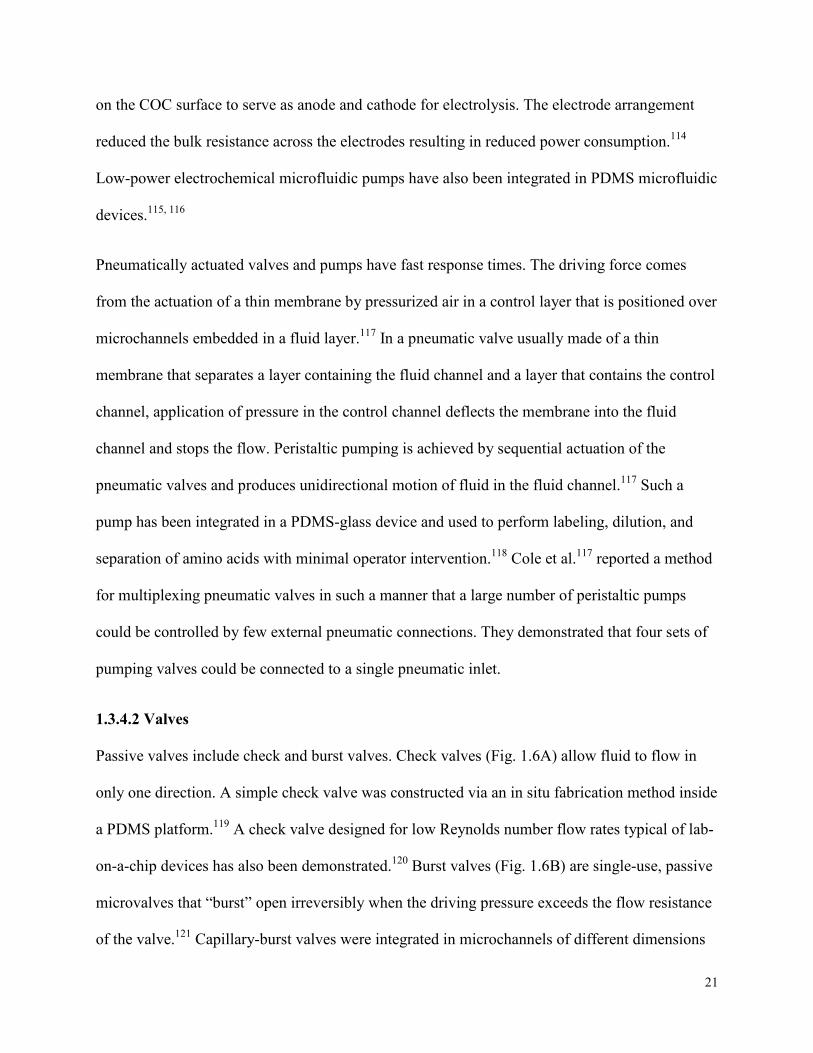
Passive valves include check and burst valves. Check valves (Fig. 1.6A) allow fluid to flow in
only one direction. A simple check valve was constructed via an in situ fabrication method inside
a PDMS platform.119 A check valve designed for low Reynolds number flow rates typical of lab-
on-a-chip devices has also been demonstrated.120 Burst valves (Fig. 1.6B) are single-use, passive
microvalves that “burst” open irreversibly when the driving pressure exceeds the flow resistance
of the valve.121 Capillary-burst valves were integrated in microchannels of different dimensions
21
and used to study the critical burst pressure or rotational speed needed to overcome the capillary
valve.122
Figure 1.6. Overview of passive and active valves. Passive valves: (A) Check valves are mechanical valves that open with unidirectional flow under differential pressure. (B) Capillary burst valves are non-mechanical valves that utilize changes in channel geometry where the valve remains closed as long as the surface tension retains the solution in the channel. Active valves: (C) Pneumatic valves utilize deflection of a membrane via application of external pressure. (D) Phase-change valves employ materials with a volume difference in a phase change; here, the valve closes as the solution is heated and the volume increases. (E) External or integrated magnets can be used for moving magnetic materials to open and close channels.
22
Active valves, like active pumps, require an external energy source with rapid response time.123
Pneumatic valves are actuated by applied pressure (Fig. 1.6C).124 A pneumatic valve positioned
at the intersection of the sample introduction and separation channels was used to control
hydrodynamic injection in a PDMS-based microchip.125 Screws embedded in the PMMA frame
of a PDMS-PMMA valve assembly have been shown to actuate pneumatic valves.126
Pneumatically actuated “lifting gate” microvalves and pumps were made by fabricating a fluidic
layer containing the gate structure and a pneumatic layer in PDMS. The microvalve structures
were then bonded to glass or plastic substrates to form microchannel structures.127 Pneumatically
actuated monolithic membrane valves have also been described.16, 17
Other active valves are phase-change (Fig. 1.6D), pinch and magnetic (Fig. 1.6E) microvalves.
Paraffin, which changes phase with temperature, was used as valving material for thermal
actuation.128 A microvalve that was actuated by the volumetric change between the solid and
liquid phases of PEG was used to couple genetic amplification and µCE.129 Pinch microvalving
is achieved by physically deforming PDMS using mechanical pressure. A variation known as
TWIST valves was used for storing and pumping fluids in PDMS devices.130 A magnetically
controlled valve was fabricated by placing a permanent magnet above the device and iron plate
beneath the device. The attractive force between the magnet and iron plate pressed a spacer
against the deformable PDMS. Valving was controlled by manually placing or removing the
permanent magnet.123
1.4 DISSERTATION OVERVIEW
Development and optimization of new materials are needed for microfluidics to gain a greater
foothold in chemical analysis outside of academia. As biological and medical applications are the
23
focus for much current research, in this dissertation I focus on the development of a material
inherently resistant to nonspecific protein adsorption. Since the material I have chosen is a
thermoplastic, formula optimization is needed to adapt this material for use with valves while
maintaining other desirable properties listed in Section 1.2.4. For greater utilization in
microfluidics, this material should be amenable to electrophoresis, capable of incorporating
valves, able to be integrated with different substrates (such as glass with electrodes for biosensor
applications), and have reduced turnaround times for rapid prototyping. This dissertation covers
my research in optimization and development of polymerized polyethylene glycol diacrylate
(poly-PEGDA) having these desirable properties for broad utilization in microfluidics.
Chapter 2 discusses my initial characterization and development of poly-PEGDA. Repeating
polyethylene glycol subunits within the polymer itself, imbue this material with reduced
nonspecific adsorption, especially compared to PDMS, whose wide use in microfluidics makes it
ideal to compare against. Resistance to protein nonspecific adsorption is demonstrated over time
and concentration for PEGDA compared to PDMS. Poly-PEGDA demonstrates resistance to
small molecule permeation and shows compatibility for use in electrophoretic separations of
peptides and proteins, the latter showing well-resolved, symmetrical peaks. Although the elastic
modulus >0.1 GPa55 for PEGDA is too high to use in self-collapsing valves, it has potential for
use in latch-valve designs.131
Since poly-PEGDA is a thermoplastic and has a Young’s modulus of ~0.13 GPa, a different type
of valve design is required compared to elastomeric polymers, such as PDMS. Chapter 3 shows
the characterization results for the fabrication of three-layer monolithic membrane valves having
both circular and square geometries. Valve performance is measured by comparing the valve
closure pressure, the input pressure in the fluidic line required to open the valve, and tracking the
24

meniscus movement over a range of applied pressures (0-30 PSI). Initially, the valve opening
pressure is ~48 kPa greater than the applied pressure to close the valve, but after an initial ~1000
actuations, this pressure difference drops to zero. Valves can be actuated at a rate of 8 Hz with a
~100 ms valve opening time and a ~20 ms closure time. The valves demonstrate good
repeatability for over 115,000 actuations.
The ability to bond poly-PEGDA to different substrates, such as silicon, glass, or other polymers,
allows for integration with a variety of different sensing mechanisms (e.g., attachment to glass
with electrodes for potentiometry or MEMS devices for biosensing). Chapter 4 introduces a
method for dual silane deposition on glass for site specific functionalization. Deposition of an
acrylate containing silane allows poly-PEGDA to bind to the glass surface, while a secondary
deposition of an aminosilane in lithographically patterned areas provides a way to attach desired
surface functionalities, such as amine-linked DNA or proteins through glutaraldehyde
crosslinking.
The fifth chapter focuses on the optimization of 3D printed poly-PEGDA microfluidic devices
having integrated valves and the adaptation of a poly-PEGDA prepolymer resin for use in 3D
printing for improved turnaround times. 3D printed devices are made utilizing a B9 Creator 3D
printer and a photosensitive resin containing poly-PEGDA in a layer-by-layer process while
changing the projected image to create different microfluidic features. 3D printing a complete
device drastically reduces total fabrication time (devices take less than 45 min to create) and
allows for rapid prototyping, where designs change frequently. Channel dimensions down to 350
µm wide by 250 µm tall were printed with a 100% success rate. Chapter 5 also contains the first
demonstration of 3D printed microfluidic valves.
25

In Chapter 6, I will discuss my conclusions about the characterization and optimization of poly-
PEGDA. The adaptation of this material for use in valves enables its broader application as a
microfluidic substrate. Heterogeneous material integration coupled with dual silane deposition
allows integration with silicon and quartz devices while providing site-specific functionalization
for further surface modification. Utilization of 3D printing in creation of poly-PEGDA devices
with integrated valves improves turnaround times for device rapid prototyping. Future directions
for the continued development of optically transparent, 3D-printed poly-PEGDA devices to
increase its allure in microfluidic applications, and one-step surface attachment to improve the
site-specific chemistry of surface functionalization will also be discussed.
1.5 REFERENCES
(1) Skoog, D. A.; Holler, F. J.; Crouch, S. R. Principles of Instrumental Analysis, 6th ed.; Thomson Brooks Cole: Belmont, CA, 2007.
(2) Guzman, N. A.; Phillips, T. M. Electrophoresis 2011, 32, 1565-1578. (3) Terry, S. C.; Jerman, J. H.; Angell, J. B. IEEE Trans. Electron Devices 1979, 26, 1880-
1886. (4) Reyes, D. R.; Iossifidis, D.; Auroux, P.-A.; Manz, A. Anal. Chem. 2002, 74, 2623-2636. (5) Harrison, D. J.; Manz, A.; Fan, Z.; Luedi, H.; Widmer, H. M. Anal. Chem. 1992, 64,
1926-1932. (6) Martinez, A. W.; Phillips, S. T.; Wiley, B. J.; Gupta, M.; Whitesides, G. M. Lab Chip
2008, 8, 2146-2150. (7) Auroux, P.-A.; Iossifidis, D.; Reyes, D. R.; Manz, A. Anal. Chem. 2002, 74, 2637-2652. (8) Vilkner, T.; Janasek, D.; Manz, A. Anal. Chem. 2004, 76, 3373-3386. (9) Dittrich, P. S.; Tachikawa, K.; Manz, A. Anal. Chem. 2006, 78, 3887-3908. (10) West, J.; Becker, M.; Tombrink, S.; Manz, A. Anal. Chem. 2008, 80, 4403-4419. (11) Arora, A.; Simone, G.; Salieb-Beugelaar, G. B.; Kim, J. T.; Manz, A. Anal. Chem. 2010,
82, 4830-4847. (12) Whitesides, G. M. Nature 2006, 442, 368-373. (13) Berthier, J.; Silberzan, P. Microfluidics for Biotechnology; Artech House: Norwood, MA,
2006, 95. (14) Placidi, M.; Cannistraro, S. Europhysics Letters 1998, 43, 476-481. (15) Madou, M. J. Fundamentals of Microfabrication: The Science of Miniaturization, 2nd
ed.; CRC Press: Boca Raton, 2002. (16) Grover, W. H.; Skelley, A. M.; Liu, C. N.; Lagally, E. T.; Mathies, R. A. Sensor Actuat
B-Chem 2003, 89, 315-323. (17) Grover, W. H.; Ivester, R. H. C.; Jensen, E. C.; Mathies, R. A. Lab Chip 2006, 6, 623-
631.
26

(18) Washburn, A. L.; Gunn, L. C.; Bailey, R. C. Anal. Chem. 2009, 81, 9499-9506. (19) Anderson, R. R.; Hu, W.; Noh, J. W.; Dahlquist, W. C.; Ness, S. J.; Gustafson, T. M.;
Richards, D. C.; Kim, S.; Mazzeo, B. A.; Woolley, A. T.; Nordin, G. P. Lab Chip 2011, 11, 2088-2096.
(20) Wang, F.; Burns, M. A. Biomed. Microdevices 2009, 11, 1071-1080. (21) Chua, J. H.; Chee, R.-E.; Agarwal, A.; Wong, S. M.; Zhang, G.-J. Anal. Chem. 2009, 81,
6266-6271. (22) Sung, J. H.; Shuler, M. L. Lab Chip 2009, 9, 1385-1394. (23) Sharma, S.; Popat, K. C.; Desai, T. A. Langmuir 2002, 18, 8728-8731. (24) Zhang, M.; Desai, T.; Ferrari, M. Biomaterials 1998, 19, 953-960. (25) Iliescu, C.; Taylor, H.; Avram, M.; Miao, J. M.; Franssila, S. Biomicrofluidics 2012, 6. (26) Effenhauser, C. S.; Bruin, G. J. M.; Paulus, A.; Ehrat, M. Anal. Chem. 1997, 69, 3451-
3457. (27) Duffy, D. C.; McDonald, J. C.; Schueller, O. J. A.; Whitesides, G. M. Anal. Chem. 1998,
70, 4974-4984. (28) Ng, J. M. K.; Gitlin, I.; Stroock, A. D.; Whitesides, G. M. Electrophoresis 2002, 23,
3461-3473. (29) Li, N.; Hsu, C.-H.; Folch, A. Electrophoresis 2005, 26, 3758-3764. (30) Araci, I. E.; Quake, S. R. Lab Chip 2012, 12, 2803-2806. (31) Cellar, N. A.; Burns, S. T.; Meiners, J.-C.; Chen, H.; Kennedy, R. T. Anal. Chem. 2005,
77, 7067-7073. (32) Hillborg, H.; Tomczak, N.; Olàh, A.; Schönherr, H.; Vancso, G. J. Langmuir 2004, 20,
785-794. (33) Berthier, E.; Young, E. W. K.; Beebe, D. Lab Chip 2012, 12, 1224-1237. (34) Roman, G. T.; Hlaus, T.; Bass, K. J.; Seelhammer, T. G.; Culbertson, C. T. Anal. Chem.
2005, 77, 1414-1422. (35) Bodas, D.; Khan-Malek, C. Microelectron. Eng. 2006, 83, 1277-1279. (36) Wang, D.; Oleschuk, R. D.; Horton, J. H. Langmuir 2008, 24, 1080-1086. (37) Sui, G.; Wang, J.; Lee, C.-C.; Lu, W.; Lee, S. P.; Leyton, J. V.; Wu, A. M.; Tseng, H.-R.
Anal. Chem. 2006, 78, 5543-5551. (38) Rolland, J. P.; Van Dam, R. M.; Schorzman, D. A.; Quake, S. R.; DeSimone, J. M. J. Am.
Chem. Soc. 2004, 126, 2322-2323. (39) Rolland, J. P.; Hagberg, E. C.; Denison, G. M.; Carter, K. R.; De Simone, J. M. Angew.
Chem. 2004, 116, 5920-5923. (40) De Marco, C.; Girardo, S.; Mele, E.; Cingolani, R.; Pisignano, D. Lab Chip 2008, 8,
1394-1397. (41) Devaraju, N. S. G. K.; Unger, M. A. Lab Chip 2011, 11, 1962-1967. (42) Dusseiller, M. R.; Schlaepfer, D.; Koch, M.; Kroschewski, R.; Textor, M. Biomaterials
2005, 26, 5917-5925. (43) Young, E. W. K.; Berthier, E.; Guckenberger, D. J.; Sackmann, E.; Lamers, C.;
Meyvantsson, I.; Huttenlocher, A.; Beebe, D. J. Anal. Chem. 2011, 83, 1408-1417. (44) Chen, C.-S.; Breslauer, D. N.; Luna, J. I.; Grimes, A.; Chin, W.-c.; Lee, L. P.; Khine, M.
Lab Chip 2008, 8, 622-624. (45) Wang, Y.; Chen, H.; He, Q.; Soper, S. A. Electrophoresis 2008, 29, 1881-1888. (46) Chen, P.-C.; Park, D. S.; You, B.-H.; Kim, N.; Park, T.; Soper, S. A.; Nikitopoulos, D.
E.; Murphy, M. C. Sens. Actuators, B 2010, 149, 291-300.
27
(47) Qi, H.; Chen, T.; Yao, L.; Zuo, T. Opt. Laser Eng. 2009, 47, 594-598. (48) Tsao, C. W.; Hromada, L.; Liu, J.; Kumar, P.; DeVoe, D. L. Lab Chip 2007, 7, 499-505. (49) Kelly, R. T.; Woolley, A. T. Anal. Chem. 2003, 75, 1941-1945. (50) Tsao, C.-W.; DeVoe, D. Microfluid. Nanofluid. 2009, 6, 1-16. (51) Brown, L.; Koerner, T.; Horton, J. H.; Oleschuk, R. D. Lab Chip 2006, 6, 66-73. (52) Yang, W.; Sun, X.; Wang, H.-Y.; Woolley, A. T. Anal. Chem. 2009, 81, 8230-8235. (53) Yang, W.; Yu, M.; Sun, X.; Woolley, A. T. Lab Chip 2010, 10, 2527-2533. (54) Kim, P.; Jeong, H. E.; Khademhosseini, A.; Suh, K. Y. Lab Chip 2006, 6, 1432-1437. (55) Kim, P.; Suh, K. Y. Langmuir 2007, 23, 4549-4553. (56) Liu, J. K.; Sun, X. F.; Lee, M. L. Anal. Chem. 2007, 79, 1926-1931. (57) Sun, X. F.; Li, D.; Lee, M. L. Anal. Chem. 2009, 81, 6278-6284. (58) Sun, X.; Farnsworth, P. B.; Woolley, A. T.; Tolley, H. D.; Warnick, K. F.; Lee, M. L.
Anal. Chem. 2007, 80, 451-460. (59) Klasner, S. A.; Metto, E. C.; Roman, G. T.; Culbertson, C. T. Langmuir 2009, 25, 10390-
10396. (60) Zhang, J.; Das, C.; Fan, Z. Microfluid. Nanofluid. 2008, 5, 327-335. (61) Liu, J.; Chen, C.-F.; Tsao, C.-W.; Chang, C.-C.; Chu, C.-C.; DeVoe, D. L. Anal. Chem.
2009, 81, 2545-2554. (62) Faure, K.; Albert, M.; Dugas, V.; Crétier, G.; Ferrigno, R.; Morin, P.; Rocca, J.-L.
Electrophoresis 2008, 29, 4948-4955. (63) Steigert, J.; Haeberle, S.; Brenner, T.; Müller, C.; Steinert, C. P.; Koltay, P.; Gottschlich,
N.; Reinecke, H.; Rühe, J.; Zengerle, R.; Ducrée, J. J. Micromech. Microeng. 2007, 17, 333.
(64) Roy, S.; Yue, C. Y. Plasma Processes Polym. 2011, 8, 432-443. (65) Carlier, J.; Arscott, S.; Thomy, V.; Fourrier, J. C.; Caron, F.; Camart, J. C.; Druon, C.;
Tabourier, P. J. Micromech. Microeng. 2004, 14, 619. (66) Ezkerra, A.; Fernandez, L. J.; Mayora, K.; Ruano-Lopez, J. M. Lab on a chip 2011, 11,
3320-3325. (67) Heyries, K. A.; Loughran, M. G.; Hoffmann, D.; Homsy, A.; Blum, L. J.; Marquette, C.
A. Biosens. Bioelectron. 2008, 23, 1812-1818. (68) Martinez, A. W.; Phillips, S. T.; Whitesides, G. M.; Carrilho, E. Anal. Chem. 2009, 82, 3-
10. (69) Pelton, R. TrAC, Trends Anal. Chem. 2009, 28, 925-942. (70) Nie, Z.; Deiss, F.; Liu, X.; Akbulut, O.; Whitesides, G. M. Lab Chip 2010, 10, 3163-
3169. (71) Klasner, S.; Price, A.; Hoeman, K.; Wilson, R.; Bell, K.; Culbertson, C. Anal. Bioanal.
Chem. 2010, 397, 1821-1829. (72) Kovarik, M. L.; Gach, P. C.; Ornoff, D. M.; Wang, Y.; Balowski, J.; Farrag, L.;
Allbritton, N. L. Anal. Chem. 2011, 84, 516-540. (73) Zhang, J. Y.; Do, J.; Premasiri, W. R.; Ziegler, L. D.; Klapperich, C. M. Lab Chip 2010,
10, 3265-3270. (74) Geiser, L.; Eeltink, S.; Svec, F.; Fréchet, J. M. J. J. Chromatogr. A 2007, 1140, 140-146. (75) Kang, Q.-S.; Li, Y.; Xu, J.-Q.; Su, L.-J.; Li, Y.-T.; Huang, W.-H. Electrophoresis 2010,
31, 3028-3034. (76) Reedy, C. R.; Hagan, K. A.; Strachan, B. C.; Higginson, J. J.; Bienvenue, J. M.;
Greenspoon, S. A.; Ferrance, J. P.; Landers, J. P. Anal. Chem. 2010, 82, 5669-5678.
28
(77) Sueyoshi, K.; Kitagawa, F.; Otsuka, K. Anal. Chem. 2008, 80, 1255-1262. (78) Chun, H.; Chung, T. D.; Ramsey, J. M. Anal. Chem. 2010, 82, 6287-6292. (79) Jacobson, S. C.; Hergenröder, R.; Moore, A. W., Jr.; Ramsey, J. M. Anal. Chem. 1994,
66, 4127-4132. (80) Yu, M.; Wang, Q.; Patterson, J. E.; Woolley, A. T. Anal. Chem. 2011, 83, 3541-3547. (81) Nge, P. N.; Pagaduan, J. V.; Yu, M.; Woolley, A. T. J. Chromatogr. A 2012, 1261, 129-
135. (82) Jacobson, S. C.; Koutny, L. B.; Hergenröder, R.; Moore, A. W., Jr.; Ramsey, J. M. Anal.
Chem. 1994, 66, 3472-3476. (83) Li, M. W.; Martin, R. S. Analyst 2008, 133, 1358-1366. (84) Mair, D. A.; Schwei, T. R.; Dinio, T. S.; Svec, F.; Fréchet, J. M. J. Lab Chip 2009, 9,
877-883. (85) Abdelgawad, M.; Watson, M. W. L.; Wheeler, A. R. Lab Chip 2009, 9, 1046-1051. (86) Lavrik, N. V.; Taylor, L. T.; Sepaniak, M. J. Anal. Chim. Acta 2011, 694, 6-20. (87) Kutter, J. P. J. Chromatogr. A 2012, 1221, 72-82. (88) Breadmore, M. C. J. Chromatogr. A 2012, 1221, 42-55. (89) Kenyon, S. M.; Meighan, M. M.; Hayes, M. A. Electrophoresis 2011, 32, 482-493. (90) Felhofer, J. L.; Blanes, L.; Garcia, C. D. Electrophoresis 2010, 31, 2469-2486. (91) Henry, C. S.; Henry, C. S., Ed.; Humana Press, 2006; Vol. 339, 1-9. (92) Ramautar, R.; de Jong, G. J.; Somsen, G. W. Electrophoresis 2012, 33, 243-250. (93) Angelescu, D. E. Highly Integrated Microfluidic Design; Artech House: Norwood, MA,
2011, 115-120. (94) Myers, F. B.; Lee, L. P. Lab Chip 2008, 8, 2015-2031. (95) Mitra, I.; Zhuang, Z.; Zhang, Y.; Yu, C.-Y.; Hammoud, Z. T.; Tang, H.; Mechref, Y.;
Jacobson, S. C. Anal. Chem. 2012, 84, 3621-3627. (96) Mainz, E. R.; Gunasekara, D. B.; Caruso, G.; Jensen, D. T.; Hulvey, M. K.; Fracassi da
Silva, J. A.; Metto, E. C.; Culbertson, A. H.; Culbertson, C. T.; Lunte, S. M. Anal. Methods 2012, 4, 414-420.
(97) García-Campaña, A. M.; Lara, F. J.; Gámiz-Gracia, L.; Huertas-Pérez, J. F. TrAC, Trends Anal. Chem. 2009, 28, 973-986.
(98) Zhao, S.; Huang, Y.; Ye, F.; Shi, M.; Liu, Y.-M. J. Chromatogr. A 2010, 1217, 5732-5736.
(99) Ohlsson, P. D.; Ordeig, O.; Mogensen, K. B.; Kutter, J. P. Electrophoresis 2009, 30, 4172-4178.
(100) Newman, C. I. D.; Giordano, B. C.; Copper, C. L.; Collins, G. E. Electrophoresis 2008, 29, 803-810.
(101) Anderson, H.; Jönsson, M.; Vestling, L.; Lindberg, U.; Aastrup, T. Sens. Actuators, B 2007, 123, 27-34.
(102) Rapp, B. E.; Gruhl, F. J.; Länge, K. Anal. Bioanal. Chem. 2010, 398, 2403-2412. (103) Ricciardi, C.; Canavese, G.; Castagna, R.; Ferrante, I.; Ricci, A.; Marasso, S. L.;
Napione, L.; Bussolino, F. Biosens. Bioelectron. 2010, 26, 1565-1570. (104) Nguyen, T.; Pei, R.; Landry, D. W.; Stojanovic, M. N.; Lin, Q. Sens. Actuators, B 2011,
154, 59-66. (105) Walker, G. M.; Beebe, D. J. Lab Chip 2002, 2, 131-134. (106) Goedecke, N.; Eijkel, J.; Manz, A. Lab Chip 2002, 2, 219-223.
29
(107) Wang, X.; Wang, S.; Gendhar, B.; Cheng, C.; Byun, C. K.; Li, G.; Zhao, M.; Liu, S. TrAC, Trends Anal. Chem. 2009, 28, 64-74.
(108) Wang, X.; Cheng, C.; Wang, S.; Liu, S. Microfluid. Nanofluid. 2009, 6, 145-162. (109) Debesset, S.; Hayden, C. J.; Dalton, C.; Eijkel, J. C. T.; Manz, A. Lab Chip 2004, 4, 396-
400. (110) Shin, W.; Lee, J. M.; Nagarale, R. K.; Shin, S. J.; Heller, A. J. Am. Chem. Soc. 2011, 133,
2374-2377. (111) Huang, C.-C.; Bazant, M. Z.; Thorsen, T. Lab Chip 2010, 10, 80-85. (112) Nestler, J.; Morschhauser, A.; Hiller, K.; Otto, T.; Bigot, S.; Auerswald, J.; Knapp, H.;
Gavillet, J.; Gessner, T. Int. J. Adv. Manuf. Technol. 2010, 47, 137-145. (113) Chiu, S.-H.; Liu, C.-H. Lab Chip 2009, 9, 1524-1533. (114) Park, S.-m.; Lee, K.; Craighead, H. Biomed. Microdevices 2008, 10, 891-897. (115) Lui, C.; Stelick, S.; Cady, N.; Batt, C. Lab Chip 2010, 10, 74-79. (116) Blanco-Gomez, G.; Glidle, A.; Flendrig, L. M.; Cooper, J. M. Anal. Chem. 2009, 81,
1365-1370. (117) Cole, M. C.; Desai, A. V.; Kenis, P. J. A. Sens. Actuators, B 2011, 151, 384-393. (118) Mora, M. F.; Greer, F.; Stockton, A. M.; Bryant, S.; Willis, P. A. Anal. Chem. 2011, 83,
8636-8641. (119) Kim, J.; Baek, J.; Lee, K.; Park, Y.; Sun, K.; Lee, T.; Lee, S. Lab Chip 2006, 6, 1091-
1094. (120) Loverich, J.; Kanno, I.; Kotera, H. Microfluid. Nanofluid. 2007, 3, 427-435. (121) Au, A. K.; Lai, H.; Utela, B. R.; Folch, A. Micromachines 2011, 2, 179-220. (122) Chen, J.; Huang, P.-C.; Lin, M.-G. Microfluid. Nanofluid. 2008, 4, 427-437. (123) Chen, C.-Y.; Chen, C.-H.; Tu, T.-Y.; Lin, C.-M.; Wo, A. M. Lab Chip 2011, 11, 733-737. (124) Ogilvie, I. R. G.; Sieben, V. J.; Cortese, B.; Mowlem, M. C.; Morgan, H. Lab Chip 2011,
11, 2455-2459. (125) Sun, X.; Kelly, R. T.; Danielson, W. F.; Agrawal, N.; Tang, K.; Smith, R. D.
Electrophoresis 2011, 32, 1610-1618. (126) Zheng, Y.; Dai, W.; Wu, H. Lab Chip 2009, 9, 469-472. (127) Kim, J.; Kang, M.; Jensen, E. C.; Mathies, R. A. Anal. Chem. 2012, 84, 2067-2071. (128) Liu, R. H.; Bonanno, J.; Yang, J.; Lenigk, R.; Grodzinski, P. Sens. Actuators, B 2004, 98,
328-336. (129) Kaigala, G. V.; Hoang, V. N.; Backhouse, C. J. Lab Chip 2008, 8, 1071-1078. (130) Weibel, D. B.; Siegel, A. C.; Lee, A.; George, A. H.; Whitesides, G. M. Lab Chip 2007,
7, 1832-1836. (131) Rogers, C. I.; Oxborrow, J. B.; Anderson, R. R.; Tsai, L. F.; Nordin, G. P.; Woolley, A.
T. Sens. Actuators, B 2014, 191, 438-444.
30
2. SINGLE-MONOMER FORMULATION OF POLYMERIZED POLYETHYLENE GLYCOL DIACRYLATE AS A NONADSORPTIVE MATERIAL FOR MICROFLUIDICS*
2.1 INTRODUCTION
The field of microfluidics has gained increasing research focus for small volume analysis over
the last 20 years.1-4 Ideally, microfluidic devices must be small and inexpensive, have rapid
analysis times, and not require extensive training to use. As specimen sizes get smaller,
microfluidics provide a means for reagent control and delivery, improved mass transport, and
more efficient sample use in small spaces. Recent examples of the power of microfluidic systems
can be found in cell-based assays,5, 6 droplet microfluidics,7-10 and chemical analysis.11-13 Goral
et al.14 used polydimethylsiloxane (PDMS) in a perfusion-based microsystem to mimic in vivo
conditions for hepatocytes without the need for special matrices or coagulants. Shi et al.15
utilized a droplet microfluidic system made from PDMS to immobilize an array of nematodes
and test the effects of varying doses of neurotoxins. Yang et al.16, 17 recently showed that
poly(methyl methacrylate) devices having photopolymerized affinity columns could be used to
selectively purify and quantitate cancer-related biomarkers from a complex sample such as blood
serum. These examples demonstrate the great potential of microfluidics in biomedical research
and point-of-care clinical analysis.
Biological samples pose a particular problem of interest for microfluidic systems. However,
PDMS, which is a popular material in these microfluidic systems, is prone to nonspecific
adsorption and fouling.18, 19 Because biological samples may be limited to very small quantities,
some or all of the analytes of interest could be lost to an adsorptive surface, instead of being
*This Chapter is reproduced with permission from Analytical Chemistry, Rogers, C. I.; Pagaduan, J. V.; Nordin, G. P.; Woolley, A. T., Anal. Chem. 2011, 83 (16), 6418-6425. Copyright 2011 American Chemical Society.
31
detected. Although many methods have attempted to address this important issue by modifying
the PDMS itself,20-24 an increasingly attractive alternative is to find a replacement material for
PDMS, which retains the ability to be patterned and formed easily, but does not suffer from
severe surface fouling.
Most current research in microfluidics uses static or dynamic surface changes to reduce
adsorption to the device material. In PDMS, plasma oxidation has been shown to increase the
hydrophilicity of the surface, but the effect is only temporary (lasting hours), because of low-
molecular-weight oligomers that are present in the bulk of the PDMS and return slowly to the
surface;25, 26 this process can be slowed if the oxidized PDMS is rapidly transferred to water.27
Solution-phase reactions can be used to functionalize oxidized PDMS surfaces with
perfluorosilanes28 or polyethylene glycol silanes.29 Dynamic surface modification methods are
by definition temporary coatings that must be replenished frequently.
Alternative materials to PDMS have been developed in the last 10 years, but they have yet to
gain significant traction. Perfluoropolymers like perfluoropolyether (PFPE)30, 31 provide inherent
resistance to nonspecific adsorption and have been used instead of PDMS as microfluidic
supports, but bonding separate layers can be problematic. Thermoset polyester microfluidic
devices32 use similar soft photolithography methods to PDMS for fabrication; however, atom-
transfer radical polymerization was needed to passivate surfaces before protein separations.33 A
mildly hydrophilic polymer, polyethylene glycol (PEG), is known for its resistance to
nonspecific binding.34 Integrating PEG directly into PDMS has been attempted, but the optical
clarity of the resulting polymer is greatly reduced.35 Incorporating PEG into an acrylate plastic
creates an optically clear, UV curable polymer that can be formed using soft lithography
techniques.36 Repeating PEG subunits in the bulk of the polymer provide an inherent way to
32
reduce nonspecific binding in fluidic pathways without further chemical modification or
replenishment. Kim et al.37 demonstrated that either PEG diacrylate (PEGDA) or PEG
dimethacrylate (PEGDMA), when mixed with a photoinitiator, could be cured quickly via UV
exposure and form stable channel features as small as 50 nm. Undercured individual layers were
bonded after they were placed together and fully cured. Poly-PEGDMA was shown to offer
lower nonspecific protein and cell adhesion than either PDMS or PEG-silanized PDMS, but no
adsorption studies on poly-PEGDA were done. Furthermore, analytical separations were not
demonstrated in either poly-PEGDMA or poly-PEGDA devices. Liu et al.36 polymerized a
multicomponent mixture of acrylate monomers, some of which included PEG groups, and
demonstrated this material’s potential as a microfluidic substrate for capillary electrophoresis.
PEG methyl ether methacrylate (PEGMEMA) was included in the formulation to extend the UV
exposure time, but methyl methacrylate (MMA), which is a more hydrophobic monomer that
lacks a PEG moiety and raises nonspecific adsorption concerns, was required to regain rigidity in
the resulting polymer.
This chapter describes the development of polymerized PEGDA (poly-PEGDA) as a
nonadsorptive alternative microfluidics material to PDMS. I demonstrated that varying the
composition of monomer and changing the photoinitiator concentration in poly-PEGDA
formulas can affect the water stability, bond strength (burst pressure), and optical clarity of the
resulting polymer. Poly-PEGDA made with a low photoinitiator concentration and three ethylene
glycol repeats (258 Da monomer) had the best combination of these properties, and was further
optimized to have background fluorescence comparable to PDMS. Importantly, poly-PEGDA
demonstrated better resistance than PDMS to permeation of small hydrophobic molecules. Innate
resistance to protein adsorption in uncoated and unmodified poly-PEGDA was demonstrated by
33
flowing increasing protein concentrations through PDMS and poly-PEGDA microchannels to
compare nonspecific adsorption over a six order-of-magnitude concentration range. Furthermore,
a low concentration (1 µg/mL) of fluorescently labeled bovine serum albumin flowed through
microchannels was utilized to illustrate the difference in nonspecific adsorption between PDMS
and poly-PEGDA over time. Poly-PEGDA exhibited a stable fluorescence signal while the
PDMS fluorescence signal increased by over 3-fold in an hour’s time. Finally, microchip
electrophoresis experiments demonstrated that poly-PEGDA sustains stable electroosmotic flow
and enables quality separations.
2.2 EXPERIMENTAL
2.2.1 Materials
Fluorescein isothiocyanate labeled bovine serum albumin (FITC-BSA), PEGDA (molecular
weight (MW) of 258), PEGMEMA (MW = 1100), MMA (99%), 2,2'-dimethoxy-2-
phenylacetophenone (DMPA), rhodamine B base (97%), DL-tryptophan (99%), dimethyl
sulfoxide (DMSO, 99.7%), porcine thyroglobulin, and β-lactoglobulin A were purchased from
Sigma-Aldrich (Milwaukee, WI). L-lysine HCl was obtained from United States Biochemical
Corporation (Cleveland, OH) and FITC was acquired from Invitrogen (Carlsbad, CA).
Anhydrous granular sodium sulfate (99.2%) and dichloromethane (99.5%) were purchased from
Mallinckrodt (Phillipsburg, NJ). Omnipur 10x phosphate buffer solution was purchased from
EMD Chemicals (Gibbstown, NJ) and diluted with deionized (DI) water (18.2 MΩ). An aqueous
saturated solution of sodium carbonate was made from powdered anhydrous sodium carbonate
(99.5%, EMD Chemicals) and DI water. Boric acid (99.5%) obtained from EM Science
(Darmstadt, Germany), sodium tetraborate decahydrate (99.5%) acquired from Sigma-Aldrich,
and DI water were used to make 25 mM borate buffer (pH 9.3). Rhodamine B base was diluted
34
in borate buffer to create a 10 µM solution. A mixture of sodium carbonate (99.5%) purchased
from EMD Chemicals, sodium bicarbonate (99.7%) obtained from EM Science, and DI water
was used to make carbonate buffers at pH 9.3 and pH 10.0. SU8-2025, SU8-2015 and SU8
developer were purchased from Microchem (Newton, MA). PDMS Sylgard 184 base and curing
agent were obtained from Dow Corning (Midland, MI).
2.2.2 PDMS Fabrication Summary
PDMS microfabrication is well known in the literature38-40 and is only summarized briefly here.
A two-layer flow channel is made, starting with fabrication of the upper PDMS layer by plasma
cleaning of a silicon wafer at 250 W for 3 min using a Planar Etch II system (Technics, San Jose,
CA). SU8-2025 was spun onto the cleaned wafer at 900 rpm to the desired thickness of 60–80
μm. A patterned chrome-coated glass mask was used to define the desired design into the
photoresist. After UV exposure for 50 s, the resist was developed in SU8 developer, leaving
raised rectangular-shaped features. The SU8 pattern formed a negative mold for the PDMS. A
4:1 ratio of PDMS to curing agent was mixed, degassed, poured over the SU8 mold and allowed
to cure at 80°C for 45 min. The ∼2-mm-thick cured PDMS was removed, cut to size using a
razor, and input and output holes were punched using a 21 gauge needle. A 3.5 in. diameter glass
wafer was plasma-cleaned as described previously. A 3:1 ratio of PDMS to curing agent was
mixed, degassed, and spun onto the wafer using a Laurell Spinner (WS-400A-6NPP-LITE, North
Wales, PA) at 2000 rpm for 60 s. This thin PDMS was allowed to cure at 80°C for 45 min. The
molded upper layer was stamped in curing agent and placed onto the lower layer, and the
combined structure was heated to 80°C for 1 h to bond the two layers together.
35

2.2.3 Poly-PEGDA Fabrication Summary
The fabrication process of a poly-PEGDA flow channel is shown in Figure 2.1. PEGDA is a
liquid that requires a mold to form structures via polymerization; the chemical structures of the
PEGDA monomer and poly-PEGDA are depicted in Figure 2.2. The flow channel mold was
made by patterning SU8-2025 on a surface (Fig. 2.1A, features “1” and “2”). A PDMS-coated
glass piece and poly-PEGDA spacers were used to define the polymerization region for the upper
layer (Fig. 2.1A, feature “3”). PDMS was coated onto the glass wafer to facilitate the removal of
the cover plate. A Karl Suss Aligner was used to expose the wafer to 10 mW/cm2 UV light. The
exposure time varied depending on the polymer thickness and formula. Once polymerized, the
poly-PEGDA was easily removed from the mold (Fig. 2.1A, feature “4”), cut into individual
dies, and holes were formed into the poly-PEGDA using a CO2 laser cutter (VersaLASER VLS
2.30, Scottsdale, AZ). Although other methods, such as using PDMS cylinders in the polymer
cast, can be used to form reservoir holes,36 laser cutting provides reproducibility and patterning
flexibility for different designs. The poly-PEGDA substrates were cleaned with isopropyl alcohol
to remove any residue or debris left on the surface. A second, unpatterned poly-PEGDA layer
was created with a similar setup to Figure 2.1A, feature “3”, but glass slides and poly-PEGDA
spacers were used to form the mold (Figs. 2.1A, features “6” and “7”). Excess liquid at the
surface of the bottom layer was removed. The poly-PEGDA layers were intentionally undercured
to help bind the two layers together subsequently; if either layer was significantly overcured,
success in irreversible bonding of the two decreased. The top layer was placed onto the bottom
layer and any bubbles that formed at the interface were extruded by gently applying pressure. A
second exposure to UV light completed the curing and bonding process (Fig. 2.1A, feature “8”).
Nanoports (Upchurch Scientific, Oak Harbor, WA) were attached to the finished poly-PEGDA
36
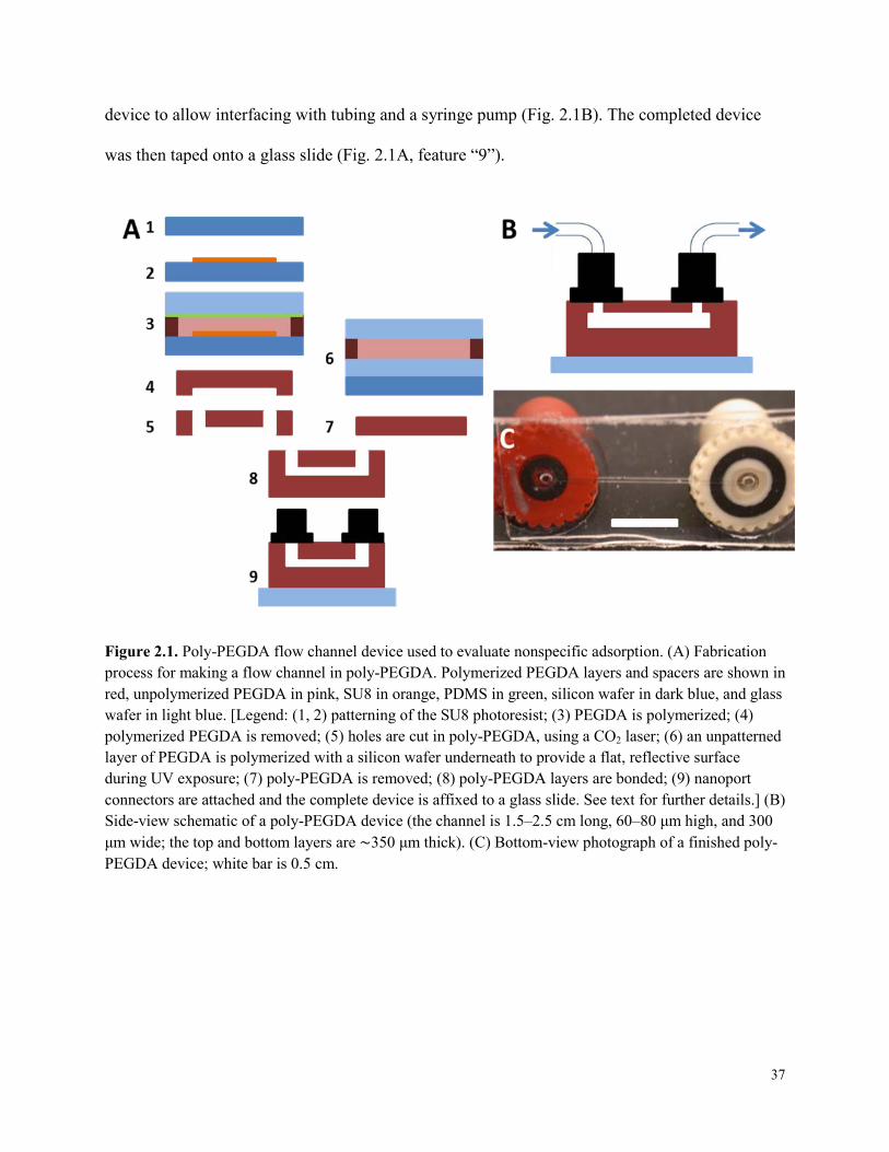
device to allow interfacing with tubing and a syringe pump (Fig. 2.1B). The completed device
was then taped onto a glass slide (Fig. 2.1A, feature “9”).
Figure 2.1. Poly-PEGDA flow channel device used to evaluate nonspecific adsorption. (A) Fabrication process for making a flow channel in poly-PEGDA. Polymerized PEGDA layers and spacers are shown in red, unpolymerized PEGDA in pink, SU8 in orange, PDMS in green, silicon wafer in dark blue, and glass wafer in light blue. [Legend: (1, 2) patterning of the SU8 photoresist; (3) PEGDA is polymerized; (4) polymerized PEGDA is removed; (5) holes are cut in poly-PEGDA, using a CO2 laser; (6) an unpatterned layer of PEGDA is polymerized with a silicon wafer underneath to provide a flat, reflective surface during UV exposure; (7) poly-PEGDA is removed; (8) poly-PEGDA layers are bonded; (9) nanoport connectors are attached and the complete device is affixed to a glass slide. See text for further details.] (B) Side-view schematic of a poly-PEGDA device (the channel is 1.5–2.5 cm long, 60–80 μm high, and 300 μm wide; the top and bottom layers are ∼350 μm thick). (C) Bottom-view photograph of a finished poly-PEGDA device; white bar is 0.5 cm.
37
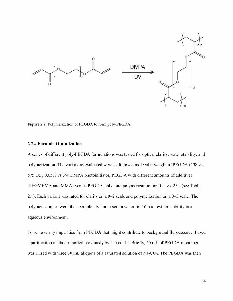
Figure 2.2. Polymerization of PEGDA to form poly-PEGDA.
2.2.4 Formula Optimization
A series of different poly-PEGDA formulations was tested for optical clarity, water stability, and
polymerization. The variations evaluated were as follows: molecular weight of PEGDA (258 vs.
575 Da), 0.05% vs 3% DMPA photoinitiator, PEGDA with different amounts of additives
(PEGMEMA and MMA) versus PEGDA-only, and polymerization for 10 s vs. 25 s (see Table
2.1). Each variant was rated for clarity on a 0–2 scale and polymerization on a 0–5 scale. The
polymer samples were then completely immersed in water for 16 h to test for stability in an
aqueous environment.
To remove any impurities from PEGDA that might contribute to background fluorescence, I used
a purification method reported previously by Liu et al.36 Briefly, 50 mL of PEGDA monomer
was rinsed with three 30 mL aliquots of a saturated solution of Na2CO3. The PEGDA was then
38
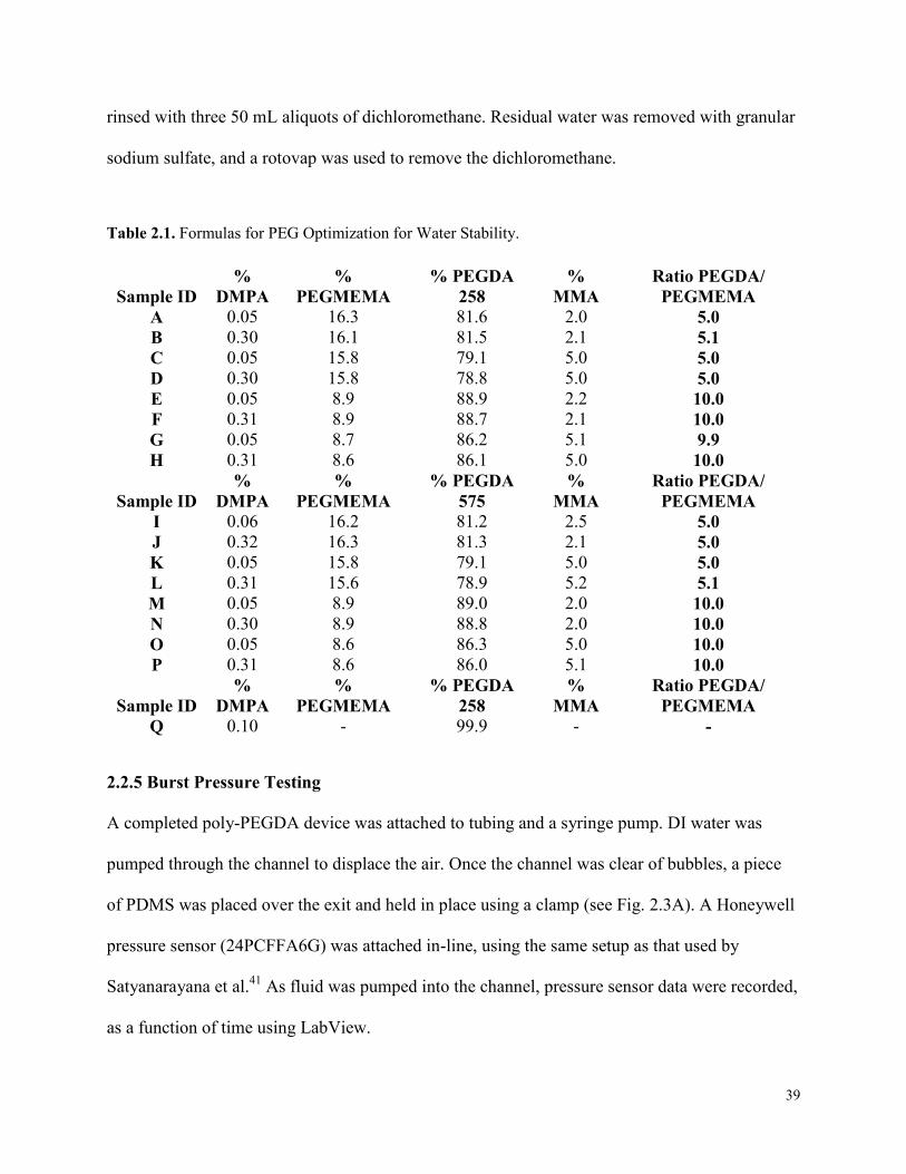
rinsed with three 50 mL aliquots of dichloromethane. Residual water was removed with granular
sodium sulfate, and a rotovap was used to remove the dichloromethane.
Table 2.1. Formulas for PEG Optimization for Water Stability.
Sample ID %
DMPA %
PEGMEMA % PEGDA
258 %
MMA Ratio PEGDA/
PEGMEMA A 0.05 16.3 81.6 2.0 5.0 B 0.30 16.1 81.5 2.1 5.1 C 0.05 15.8 79.1 5.0 5.0 D 0.30 15.8 78.8 5.0 5.0 E 0.05 8.9 88.9 2.2 10.0 F 0.31 8.9 88.7 2.1 10.0 G 0.05 8.7 86.2 5.1 9.9 H 0.31 8.6 86.1 5.0 10.0
Sample ID %
DMPA %
PEGMEMA % PEGDA
575 %
MMA Ratio PEGDA/
PEGMEMA I 0.06 16.2 81.2 2.5 5.0 J 0.32 16.3 81.3 2.1 5.0 K 0.05 15.8 79.1 5.0 5.0 L 0.31 15.6 78.9 5.2 5.1 M 0.05 8.9 89.0 2.0 10.0 N 0.30 8.9 88.8 2.0 10.0 O 0.05 8.6 86.3 5.0 10.0 P 0.31 8.6 86.0 5.1 10.0
Sample ID %
DMPA %
PEGMEMA % PEGDA
258 %
MMA Ratio PEGDA/
PEGMEMA Q 0.10 - 99.9 - -
2.2.5 Burst Pressure Testing
A completed poly-PEGDA device was attached to tubing and a syringe pump. DI water was
pumped through the channel to displace the air. Once the channel was clear of bubbles, a piece
of PDMS was placed over the exit and held in place using a clamp (see Fig. 2.3A). A Honeywell
pressure sensor (24PCFFA6G) was attached in-line, using the same setup as that used by
Satyanarayana et al.41 As fluid was pumped into the channel, pressure sensor data were recorded,
as a function of time using LabView.
39
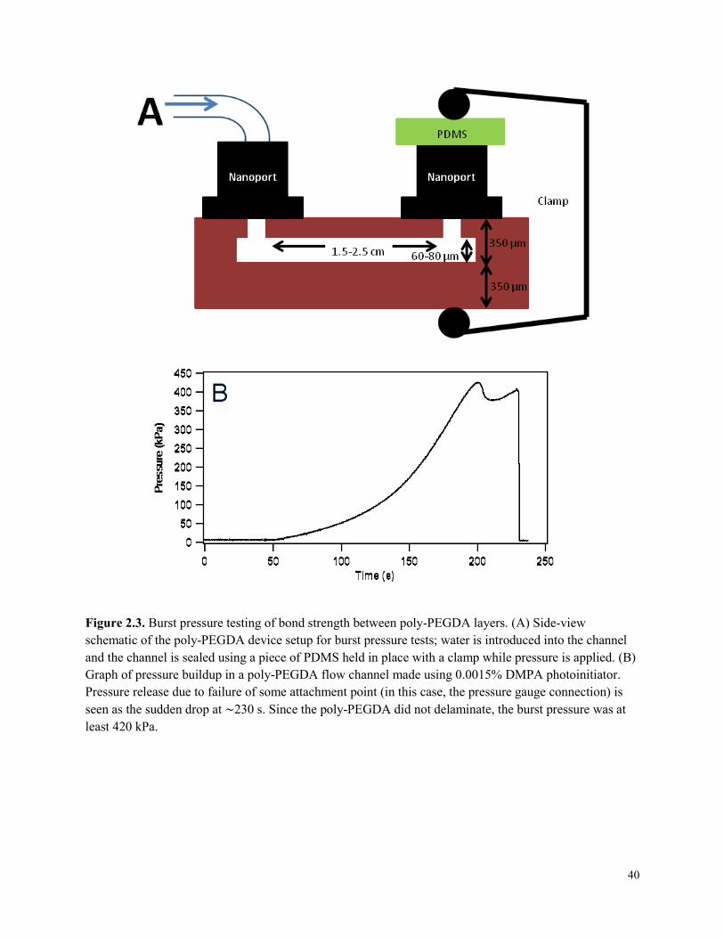
Figure 2.3. Burst pressure testing of bond strength between poly-PEGDA layers. (A) Side-view schematic of the poly-PEGDA device setup for burst pressure tests; water is introduced into the channel and the channel is sealed using a piece of PDMS held in place with a clamp while pressure is applied. (B) Graph of pressure buildup in a poly-PEGDA flow channel made using 0.0015% DMPA photoinitiator. Pressure release due to failure of some attachment point (in this case, the pressure gauge connection) is seen as the sudden drop at ∼230 s. Since the poly-PEGDA did not delaminate, the burst pressure was at least 420 kPa.
40
2.2.6 Bulk Fluorescence Comparison
To test bulk fluorescence properties, 700-µm-thick layers were formed of PDMS, poly-PEGDA
made with 1% DMPA, and poly-PEGDA made with purified monomer and 1% DMPA. Regions
illuminated by a Reliant 150 M 488 nm laser (Laser Physics, West Jordan, UT) expanded to a
∼1.4-mm-diameter diffuse beam were imaged using a CoolSNAPHQ CCD (Photometrics,
Tucson, AZ). The power of the laser at the detection point was 1 mW. After initial images, the
devices were exposed to ∼3.5 mW at the detection point for 30 min to survey for any
photobleaching once the power was returned to 1 mW and additional fluorescence images were
taken.
2.2.7 Rhodamine B Comparison
Roman et al.42 demonstrated that hydrophobic molecules such as rhodamine B can readily
diffuse into PDMS. I used a similar method to compare the diffusion of rhodamine B into poly-
PEGDA and PDMS. A 50-µm-wide, ∼20-µm-tall, and 3.0-cm-long feature made from patterned
SU8-2015 was used to cast channels in both materials. Fluorescence images using the same
laser/CCD setup as above were obtained for the channels under flow (0.2 µL/min) of borate
buffer (0 min) and 10 µM rhodamine B at several time intervals up to 4 h. The laser was blocked
between measurements to avoid photobleaching.
2.2.8 Fluorescence Comparison
PDMS and poly-PEGDA two-layer devices, each having a flow channel, were used to compare
nonspecific binding on channel surfaces. Laser-induced fluorescence (LIF) at 488 nm, as
described in Section 2.2.6, was used to detect nonspecific adsorption of FITC-BSA. Background
signal for the polymer in each device was photobleached by raising the laser power from 1 mW
to 3.5 mW at the detection point for 15 min.
41
A series of exposures to increasing concentrations of FITC-BSA followed by buffer rinses was
used to compare nonspecific binding for PDMS and poly-PEGDA. Initially, 1x PBS solution was
rinsed through the flow channel at a rate of 110 µL/min for 3 min. The flow was reduced to
10 µL/min and allowed to flow for 1 min before a fluorescence image was taken. A sample of 1
ng/mL FITC-BSA was introduced in the same fashion and allowed to sit in the channel with no
flow for 5 min. An image was taken after resuming flow for 1 min at 10 µL/min. The laser was
blocked except during fluorescence measurement to avoid photobleaching of surface-adsorbed
molecules. PBS was then used to rinse the channel as described previously, and another image
was taken with buffer only in the channel. These steps were repeated for FITC-BSA
concentrations increasing from 3 ng/mL to 1 mg/mL. The fluorescence images from the CCD
were analyzed using ImageJ 1.43u. In all cases, background images were captured with buffer
flowing in the channel at 10 µL/min, and the resulting background signal was subtracted from
the sample fluorescent images.
2.2.9 Time Comparison
A low concentration of a model adsorptive species (FITC-BSA), flowed slowly through a
microchannel, enables the determination of the time dependence of nonspecific binding for a
substrate. The flow rate was set such that diffusional transport would allow FITC-BSA
throughout the channel to interact with the surface prior to the detection location. The equation
for diffusion in one dimension is given by Eq. 1.1 in Section 1.1 where x is distance, D is the
diffusion coefficient, and t the time.43 A value of D = 6 x 10⁻⁷ cm2/s was used for FITC-BSA.44
Rearranging Eq. 1.1 to solve for t gives the time for a molecule to diffuse across a distance x. In
this channel geometry, ∼27 s are required for a FITC-BSA molecule to diffuse 80 µm (top to
bottom surface), and just ∼7 s are needed to travel 40 µm (midchannel to wall). FITC-BSA in
42
solution flowing at 0.2 µL/min to the shortest distance to detection (0.2 cm) would take ∼14 s to
arrive, thus allowing adequate time for any given FITC-BSA molecule to come into contact with
the channel surface prior to the detection point.
The flow channel and detection setup were the same as that described in Sections 2.2.6 and 2.2.8.
The channel was rinsed with PBS for 10 min at 100 µL/min to remove any bubbles or debris.
After rinsing, an air bubble was introduced into the channel before a 1 µg/mL solution of FITC-
BSA (to signal when the sample had entered the channel). Data acquisition started when the
bubble was visible in the channel but before the fluorescent sample had entered the detection
zone. Images were taken every minute for poly-PEGDA, and every minute for PDMS for the
first 35 min, with images taken every 5 or 10 min thereafter.
2.2.10 Microchip Electrophoresis
Lysine and tryptophan at 1 mg/mL in carbonate buffer (pH 9.3) were labeled with 4 mg/mL
FITC in DMSO by mixing 25 µL of FITC solution with 75 µL of amino acid solution and
reacting at room temperature for 24 h.16 β-lactoglobulin A (2 mg/mL) was labeled with FITC by
mixing 5 µL of FITC solution with 100 µL of protein solution, while thyroglobulin was labeled
by mixing 10 µL of FITC solution with 100 µL of 2 mg/mL thyroglobulin. Protein solutions
were then filtered to remove excess FITC using a 3 kDa Amicon Ultra filter (Billerica, MA).
Protein concentrations were quantified using a Nanodrop ND-1000 spectrophotometer
(Wilmington, DE).
The offset-T design electrophoresis microchip45 was fabricated in poly-PEGDA, as described in
Section 2.2.7 for the rhodamine B test devices. The injection arms were 0.5 cm long, and the
separation channel was 3.0 cm from the intersection to the end reservoir. The channels were 50
43
µm wide and 18 µm tall. Pinched injection times of 20 s for amino acids and 30 s for proteins
were used to introduce the analytes into the separation channel. The amino acid separation
used -850 V across the injection pathway, -2000 V along the separation channel, and pH 9.3
carbonate buffer. Protein analysis was done using -900 V for injection and -2000 V for
separation with pH 10.0 carbonate buffer. Fluorescence was collected at a separation distance of
2.5 cm using a point detection system described previously.45
2.3 RESULTS AND DISCUSSION
2.3.1 Formula Optimization
The polymer formulation is critical to achieving the desired device properties. If a higher
molecular weight of PEGDA (i.e., 575 or 700 Da) is used (see Tables 2.2 and 2.3), the resulting
polymer is susceptible to swelling, and eventual buckling and cracking when exposed to water,
typically within as little as 10 min of submersion (similar to results from Kim et al.37). The
concentration of DMPA affected the rate of polymerization: higher concentrations required
shorter UV exposure times but generated heat which resulted in cracking of the polymer
material. The addition of PEGMEMA increased the UV exposure time but required the use of
MMA in higher concentrations for structural stability. By comparing a series of formulations
including PEGDA-only, I determined an optimal formula for making thin (∼350 µm) layers
while maintaining optical clarity and water stability. Scanning electron microscopy (SEM)
images detail channel features in poly-PEGDA (see Fig. 2.4).
Poly-PEGDA made from a low-molecular-weight PEGDA (258 Da) and having 0.0015%–
1.0% DMPA photoinitiator was found to be the most stable in water while still having good
optical clarity (see Fig. 2.5). Although three other polymer formulations that also contained
PEGMEMA and MMA in addition to PEGDA survived submersion for more than 16 h, the
44
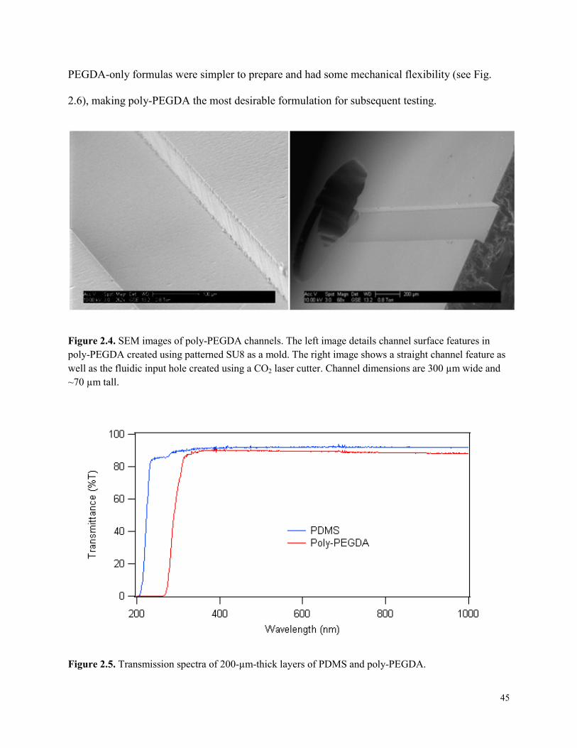
PEGDA-only formulas were simpler to prepare and had some mechanical flexibility (see Fig.
2.6), making poly-PEGDA the most desirable formulation for subsequent testing.
Figure 2.4. SEM images of poly-PEGDA channels. The left image details channel surface features in poly-PEGDA created using patterned SU8 as a mold. The right image shows a straight channel feature as well as the fluidic input hole created using a CO2 laser cutter. Channel dimensions are 300 µm wide and ~70 µm tall.
Figure 2.5. Transmission spectra of 200-µm-thick layers of PDMS and poly-PEGDA.
45

Figure 2.6. Mechanical flexibility. Flexibility of poly-PEGDA is demonstrated as pressure is applied to a 350 µm thick layer.
Table 2.2. Results for PEG Optimization for Water Stability with 10 s Exposure Time.
Sample ID Polymerization Clarity Water Immersion
Test Comments A 1 0 <0.5 min Became white B 5 1 >10 min Survived C 1 0 <0.5 min Became white D 5 0 >10 min Survived E 0 0 <0.5 min Became white F 5 1 >10 min Survived G 0 0 <0.5 min Became white H 5 0 <0.5 min Became white
I 1 0 >10 min Survived but not
completely polymerized J 4 0 1:10 min Buckled K 1 0 4 min Buckled L 3 0 <1 min Buckled M 2 2 >10 min Really soft N 4 1 4:30 min Buckled O 2 0 4 min Buckled P 4 0 1 min Buckled Q 5 0 >10 min Survived
46

Table 2.3. Results for PEG Optimization for Water Stability with 25 s Exposure Time.
Sample ID Polymerization Clarity Water Immersion
Test Comments A 5 1 >10 min Survived B 5 2 >10 min Survived
C 3 0 >10 min Survived but really soft when
removed from wafer D 5 1 >10 min Survived E 5 1 >10 min Survived F 5 2 >10 min Survived G 3 1 <0.5 min Turned white H 5 1 >10 min Survived I 3 0 1:30 min Buckled J 5 0 7 min Buckled K 3 0 6:30 min Buckled L 4 0 2:18 min Buckled M 5 1 4 min Buckled N 5 0 >10 min Survived O 3 0 3 min Buckled
P 5 0 >10 min Some separation from silicon
but no buckling Q 5 0 >10 min Survived
2.3.2 Burst Pressure Tests
Burst pressure measurement provided a way to evaluate the bond strength between two layers by
pressurizing a liquid into the interface between them. Recent work by Tsai et al.46 showed that
burst pressure—and, therefore bond strength—of PDMS is largely dependent on the method
used to bind two layers. The burst pressure for silicon with PDMS cured without heat or
adhesive is relatively weak at ∼50 kPa. When PDMS curing agent is used as an adhesive and
cured at room temperature for 16 h, the silicon-PDMS burst pressure increases to ∼430 kPa.
Heat curing at 90 ºC for 30 min can raise the silicon-PDMS burst pressure even further to
770 kPa, but heat curing techniques are not compatible with protein functionalized surfaces.
Pressures in the poly-PEGDA flow channel reached up to 420 kPa (Fig. 2.3B) before the
pressure sensor became disconnected from the tubing. It should be noted that, since the pressure
47
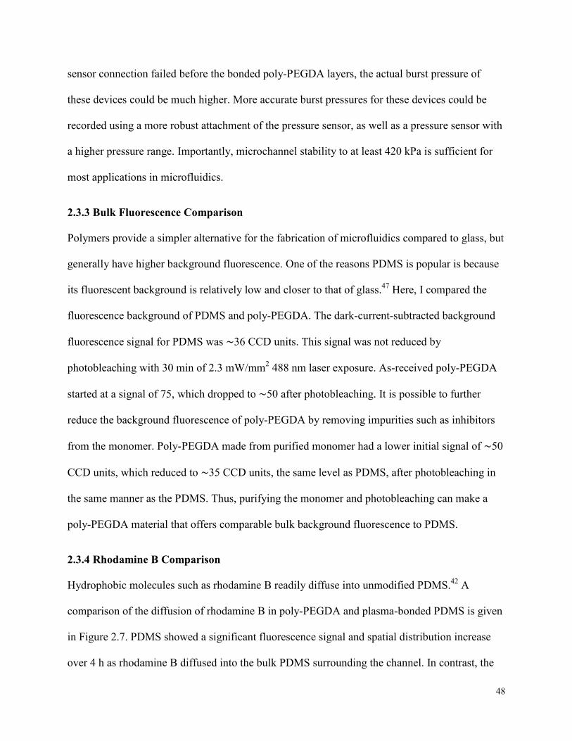
sensor connection failed before the bonded poly-PEGDA layers, the actual burst pressure of
these devices could be much higher. More accurate burst pressures for these devices could be
recorded using a more robust attachment of the pressure sensor, as well as a pressure sensor with
a higher pressure range. Importantly, microchannel stability to at least 420 kPa is sufficient for
most applications in microfluidics.
2.3.3 Bulk Fluorescence Comparison
Polymers provide a simpler alternative for the fabrication of microfluidics compared to glass, but
generally have higher background fluorescence. One of the reasons PDMS is popular is because
its fluorescent background is relatively low and closer to that of glass.47 Here, I compared the
fluorescence background of PDMS and poly-PEGDA. The dark-current-subtracted background
fluorescence signal for PDMS was ∼36 CCD units. This signal was not reduced by
photobleaching with 30 min of 2.3 mW/mm2 488 nm laser exposure. As-received poly-PEGDA
started at a signal of 75, which dropped to ∼50 after photobleaching. It is possible to further
reduce the background fluorescence of poly-PEGDA by removing impurities such as inhibitors
from the monomer. Poly-PEGDA made from purified monomer had a lower initial signal of ∼50
CCD units, which reduced to ∼35 CCD units, the same level as PDMS, after photobleaching in
the same manner as the PDMS. Thus, purifying the monomer and photobleaching can make a
poly-PEGDA material that offers comparable bulk background fluorescence to PDMS.
2.3.4 Rhodamine B Comparison
Hydrophobic molecules such as rhodamine B readily diffuse into unmodified PDMS.42 A
comparison of the diffusion of rhodamine B in poly-PEGDA and plasma-bonded PDMS is given
in Figure 2.7. PDMS showed a significant fluorescence signal and spatial distribution increase
over 4 h as rhodamine B diffused into the bulk PDMS surrounding the channel. In contrast, the
48
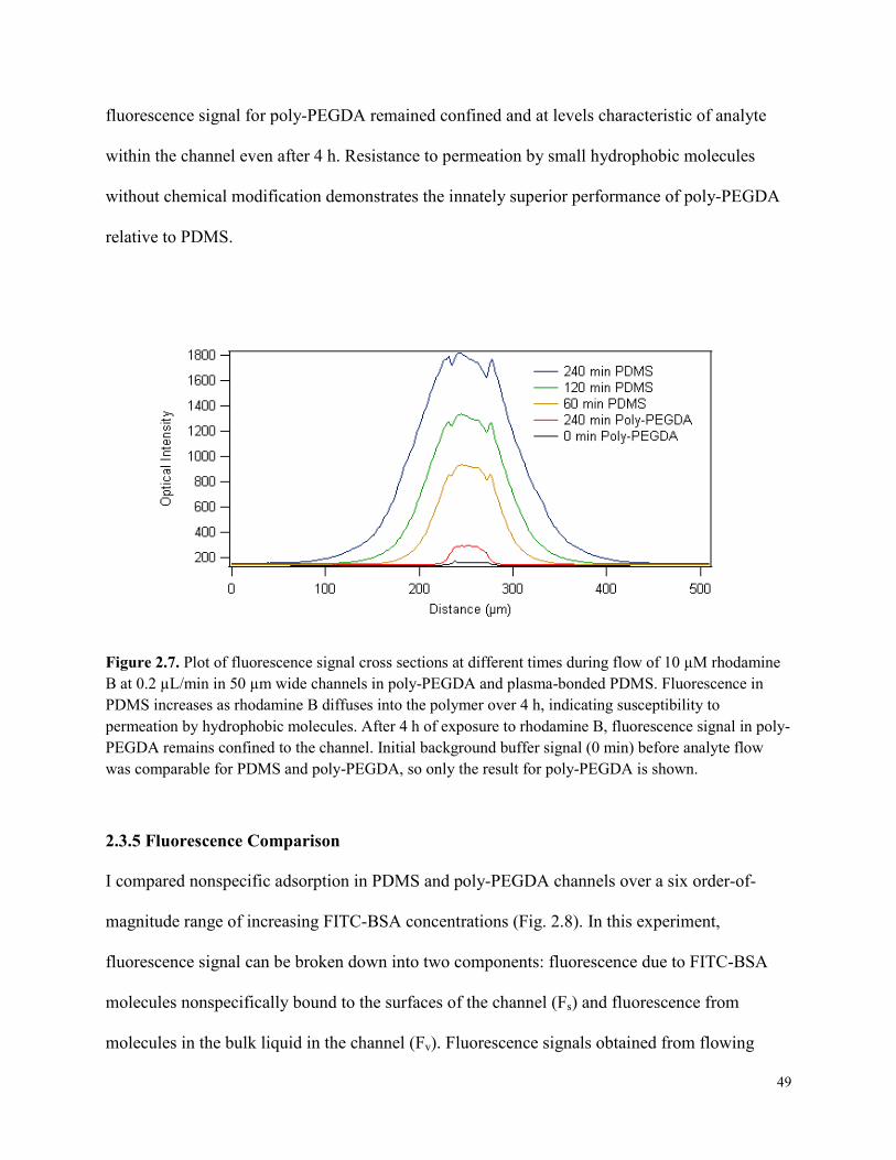
fluorescence signal for poly-PEGDA remained confined and at levels characteristic of analyte
within the channel even after 4 h. Resistance to permeation by small hydrophobic molecules
without chemical modification demonstrates the innately superior performance of poly-PEGDA
relative to PDMS.
Figure 2.7. Plot of fluorescence signal cross sections at different times during flow of 10 µM rhodamine B at 0.2 µL/min in 50 µm wide channels in poly-PEGDA and plasma-bonded PDMS. Fluorescence in PDMS increases as rhodamine B diffuses into the polymer over 4 h, indicating susceptibility to permeation by hydrophobic molecules. After 4 h of exposure to rhodamine B, fluorescence signal in poly-PEGDA remains confined to the channel. Initial background buffer signal (0 min) before analyte flow was comparable for PDMS and poly-PEGDA, so only the result for poly-PEGDA is shown.
2.3.5 Fluorescence Comparison
I compared nonspecific adsorption in PDMS and poly-PEGDA channels over a six order-of-
magnitude range of increasing FITC-BSA concentrations (Fig. 2.8). In this experiment,
fluorescence signal can be broken down into two components: fluorescence due to FITC-BSA
molecules nonspecifically bound to the surfaces of the channel (Fs) and fluorescence from
molecules in the bulk liquid in the channel (Fv). Fluorescence signals obtained from flowing
49
FITC-BSA sample solutions contain both Fs and Fv, while signals from the PBS rinse consist of
only Fs. Theoretically Fv should provide a linear increase in fluorescence with concentration
resulting in a slope of 1 as long as Fs = 0. After only a 5-min exposure to the lowest FITC-BSA
concentration (1 ng/mL) and flowing at 10 µL/min for 1 min, the background-subtracted
fluorescence signal for PDMS was already higher than the detector noise level (the standard
deviation of the signal prior to background subtraction). In contrast, poly-PEGDA exposed to
FITC-BSA concentrations under 100 ng/mL exhibited background subtracted fluorescence
below the level of detector noise. Only at FITC-BSA concentrations above ∼50 µg/mL was the
signal due to protein in the PDMS channel greater than the signal due to FITC-BSA
nonspecifically bound to the walls (Fv > Fs). In contrast, the protein solution signal is distinct
from Fs above ∼10 µg/mL FITC-BSA in poly-PEGDA, indicating lower levels of nonspecific
adsorption. The slope of signal as a function of FITC-BSA concentration is well below 1 in
PDMS, because of significant nonspecific adsorption at lower concentrations (Fs ≠ 0), leading to
much higher signals observed than would be expected from the channel contents alone (Fv). For
just the highest two FITC-BSA concentrations (≥500 µg/mL), the signal versus concentration
plot has the slope of 0.94 (∼1) for PDMS. For poly-PEGDA exposed to FITC-BSA, the signal
versus concentration slope from 50 µg/mL to 1 mg/mL was 0.91 (∼1), offering an order-of-
magnitude larger linear range than in PDMS. This result clearly demonstrates less nonspecific
adsorption in poly-PEGDA, making this material better suited for quantitative measurements on
adsorptive proteins.
50

Figure 2.8. Background-subtracted fluorescence signal in PDMS and poly-PEGDA microdevices for increasing FITC-BSA concentrations. The standard deviation of signal before background subtraction is shown as a dashed line. In poly-PEGDA, the signal for 1 ng/mL FITC-BSA was at the level of dark current and was not plotted.
2.3.6 Time Comparison
PDMS and poly-PEGDA behaved differently when exposed to flow of a low concentration of
FITC-BSA over time (Fig. 2.9). This experiment thus expands over a prior publication,37 where
only the end results of nonspecific adsorption were reported. The steady increase in fluorescence
signal in the PDMS device was due to nonspecific adsorption of FITC-BSA to the channel
surface in the detection window (Fs ≠ 0). The fluorescence signal for FITC-BSA in the PDMS
channel was initially less than in the poly-PEGDA channel but it slowly increased to three times
the poly-PEGDA amount within 100 min. The initially lower signal in PDMS during the first
∼20 min was most likely due to depletion of FITC-BSA flowing in the channel, through surface
adsorption prior to the detection point. The PDMS signal was detected 2 mm from the sample
51
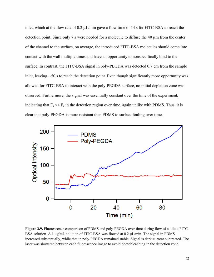
inlet, which at the flow rate of 0.2 µL/min gave a flow time of 14 s for FITC-BSA to reach the
detection point. Since only 7 s were needed for a molecule to diffuse the 40 µm from the center
of the channel to the surface, on average, the introduced FITC-BSA molecules should come into
contact with the wall multiple times and have an opportunity to nonspecifically bind to the
surface. In contrast, the FITC-BSA signal in poly-PEGDA was detected 0.7 cm from the sample
inlet, leaving ∼50 s to reach the detection point. Even though significantly more opportunity was
allowed for FITC-BSA to interact with the poly-PEGDA surface, no initial depletion zone was
observed. Furthermore, the signal was essentially constant over the time of the experiment,
indicating that Fs << Fv in the detection region over time, again unlike with PDMS. Thus, it is
clear that poly-PEGDA is more resistant than PDMS to surface fouling over time.
Figure 2.9. Fluorescence comparison of PDMS and poly-PEGDA over time during flow of a dilute FITC-BSA solution. A 1 μg/mL solution of FITC-BSA was flowed at 0.2 μL/min. The signal in PDMS increased substantially, while that in poly-PEGDA remained stable. Signal is dark-current-subtracted. The laser was shuttered between each fluorescence image to avoid photobleaching in the detection zone.
52
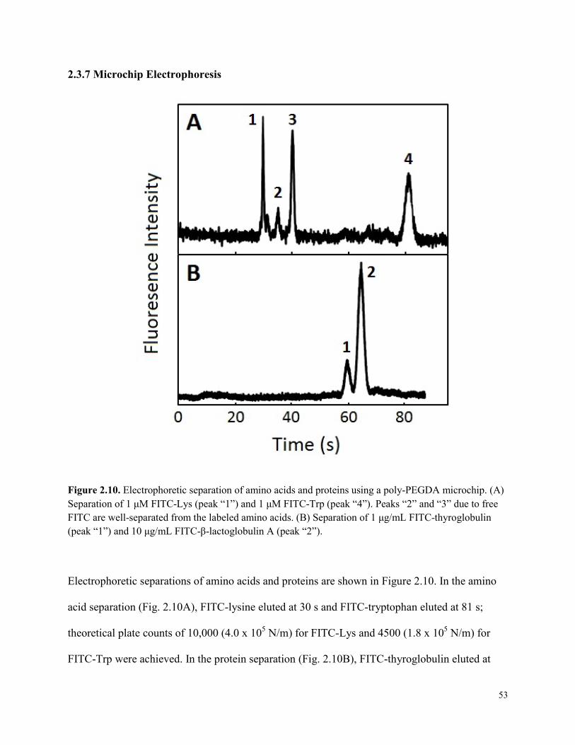
2.3.7 Microchip Electrophoresis
Figure 2.10. Electrophoretic separation of amino acids and proteins using a poly-PEGDA microchip. (A) Separation of 1 μM FITC-Lys (peak “1”) and 1 μM FITC-Trp (peak “4”). Peaks “2” and “3” due to free FITC are well-separated from the labeled amino acids. (B) Separation of 1 μg/mL FITC-thyroglobulin (peak “1”) and 10 μg/mL FITC-β-lactoglobulin A (peak “2”).
Electrophoretic separations of amino acids and proteins are shown in Figure 2.10. In the amino
acid separation (Fig. 2.10A), FITC-lysine eluted at 30 s and FITC-tryptophan eluted at 81 s;
theoretical plate counts of 10,000 (4.0 x 10⁵ N/m) for FITC-Lys and 4500 (1.8 x 10⁵ N/m) for
FITC-Trp were achieved. In the protein separation (Fig. 2.10B), FITC-thyroglobulin eluted at
53
59 s and FITC-β-lactoglobulin A eluted at 64 s, with a resolution of 1.4. Theoretical plate
numbers were 4900 (2.0 x 10⁵ N/m) for FITC-thyroglobulin and 4400 (1.8 x 10⁵ N/m) for FITC-
β-lactoglobulin A. In comparison, Wang et al.48 demonstrated that unmodified PDMS gave poor
resolution for both amino acids and proteins. They further showed that modifying PDMS
surfaces with chitosan improved the resolution, but their best theoretical plate counts were much
smaller at 6.2 x 10⁴ N/m for an amino acid and 2.2 x 10⁴ N/m for a protein. The theoretical plate
counts for unmodified poly-PEGDA indicate great promise for use of this material in high-
performance separations.
2.4 CONCLUSIONS
A material formed from photopolymerization of poly(ethylene glycol) diacrylate (poly-PEGDA)
was made using a similar fabrication process to polydimethylsiloxane (PDMS). Poly-PEGDA
was shown to be stable in water, have a high burst pressure (bond strength), and have optical
clarity similar to PDMS. Poly-PEGDA also demonstrated excellent resistance to diffusion of
small hydrophobic molecules into the bulk material, lower nonspecific binding than PDMS over
a range of increasing adsorptive protein concentrations, and greater resistance over time to
surface fouling during exposure to low protein concentrations. Poly-PEGDA shares with PDMS
the favorable characteristic of low intrinsic fluorescent background. Finally, symmetric peaks
and theoretical plate counts in electrophoretic separations of amino acids and proteins
demonstrate the value of poly-PEGDA for biological sample analysis.
Low nonspecific adsorption, coupled with low background fluorescence for poly-PEGDA,
makes this polymer worthy of consideration as an alternative to PDMS for microfluidic devices.
An important feature of PDMS is its elasticity, which allows for the implementation of valves
and pumps into microsystems. These poly-PEGDA layers similarly have some elasticity, as
54
demonstrated by the ability to flex or bend without breaking. Further optimization of poly-
PEGDA formulations is ongoing to provide comparable mechanical properties to PDMS.
Creating flexible valves and pumps entirely from poly-PEGDA would allow fewer areas for
analyte adsorption and contribute to lower detection limits. The integration of nonadsorptive
microfluidic materials, such as poly-PEGDA, with analyte sensing mechanisms such as
microcantilevers or nanowires should provide broader application and further enable the
evaluation of new detection modalities in biomedical research.
2.5 REFERENCES
(1) Reyes, D. R.; Iossifidis, D.; Auroux, P.-A.; Manz, A. Anal. Chem. 2002, 74, 2623-2636. (2) Arora, A.; Simone, G.; Salieb-Beugelaar, G. B.; Kim, J. T.; Manz, A. Anal. Chem. 2010,
82, 4830-4847. (3) Wang, J.; Ren, L.; Li, L.; Liu, W.; Zhou, J.; Yu, W.; Tong, D.; Chen, S. Lab Chip 2009,
9, 644-652. (4) Lindström, S.; Andersson-Svahn, H. Lab Chip 2010, 10, 3363-3372. (5) Anglin, E. J.; Salisbury, C.; Bailey, S.; Hor, M.; Macardle, P.; Fenech, M.; Thissen, H.;
Voelcker, N. H. Lab Chip 2010, 10, 3413-3421. (6) Dudek, M. M.; Kent, N.; Gustafsson, K. M.; Lindahl, T. L.; Killard, A. J. Anal. Chem.
2010, 83, 319-328. (7) Teh, S.-Y.; Lin, R.; Hung, L.-H.; Lee, A. P. Lab Chip 2008, 8, 198-220. (8) Pei, J.; Nie, J.; Kennedy, R. T. Anal. Chem. 2010, 82, 9261-9267. (9) Huebner, A.; Bratton, D.; Whyte, G.; Yang, M.; deMello, A. J.; Abell, C.; Hollfelder, F.
Lab Chip 2009, 9, 692-698. (10) Jeffries, G. D. M.; Lorenz, R. M.; Chiu, D. T. Anal. Chem. 2010, 82, 9948-9954. (11) Benhabib, M.; Chiesl, T. N.; Stockton, A. M.; Scherer, J. R.; Mathies, R. A. Anal. Chem.
2010, 82, 2372-2379. (12) Bruzewicz, D. A.; Reches, M.; Whitesides, G. M. Anal. Chem. 2008, 80, 3387-3392. (13) Mellors, J. S.; Jorabchi, K.; Smith, L. M.; Ramsey, J. M. Anal. Chem. 2010, 82, 967-973. (14) Goral, V. N.; Hsieh, Y.-C.; Petzold, O. N.; Clark, J. S.; Yuen, P. K.; Faris, R. A. Lab
Chip 2010, 10, 3380-3386. (15) Shi, W.; Wen, H.; Lu, Y.; Shi, Y.; Lin, B.; Qin, J. Lab Chip 2010, 10, 2855-2863. (16) Yang, W.; Sun, X.; Wang, H.-Y.; Woolley, A. T. Anal. Chem. 2009, 81, 8230-8235. (17) Yang, W.; Yu, M.; Sun, X.; Woolley, A. T. Lab Chip 2010, 10, 2527-2533. (18) Sia, S. K.; Whitesides, G. M. Electrophoresis 2003, 24, 3563-3576. (19) Huang, B.; Wu, H.; Kim, S.; Zare, R. N. Lab Chip 2005, 5, 1005-1007. (20) Phillips, K. S.; Kang, K. M.; Licata, L.; Allbritton, N. L. Lab Chip 2010, 10, 864-870. (21) Roman, G. T.; Culbertson, C. T. Langmuir 2006, 22, 4445-4451. (22) Séguin, C.; McLachlan, J. M.; Norton, P. R.; Lagugné-Labarthet, F. Appl. Surf. Sci. 2010,
256, 2524-2531.
55

(23) Barbier, V.; Tatoulian, M.; Li, H.; Arefi-Khonsari, F.; Ajdari, A.; Tabeling, P. Langmuir 2006, 22, 5230-5232.
(24) Kim, B.-Y.; Hong, L.-Y.; Chung, Y.-M.; Kim, D.-P.; Lee, C.-S. Adv. Funct. Mater. 2009, 19, 3796-3803.
(25) Bodas, D.; Khan-Malek, C. Microelectron. Eng. 2006, 83, 1277-1279. (26) Hillborg, H.; Tomczak, N.; Olàh, A.; Schönherr, H.; Vancso, G. J. Langmuir 2004, 20,
785-794. (27) Bausch, G. G.; Stasser, J. L.; Tonge, J. S.; Owen, M. J. Plasmas and Polymers 1998, 3,
23-34. (28) Wang, D.; Oleschuk, R. D.; Horton, J. H. Langmuir 2008, 24, 1080-1086. (29) Sui, G.; Wang, J.; Lee, C.-C.; Lu, W.; Lee, S. P.; Leyton, J. V.; Wu, A. M.; Tseng, H.-R.
Anal. Chem. 2006, 78, 5543-5551. (30) Truong, T. T.; Lin, R.; Jeon, S.; Lee, H. H.; Maria, J.; Gaur, A.; Hua, F.; Meinel, I.;
Rogers, J. A. Langmuir 2007, 23, 2898-2905. (31) Willis, P. A.; Greer, F.; Lee, M. C.; Smith, J. A.; White, V. E.; Grunthaner, F. J.;
Sprague, J. J.; Rolland, J. P. Lab Chip 2008, 8, 1024-1026. (32) Fiorini, G. S.; Lorenz, R. M.; Kuo, J. S.; Chiu, D. T. Anal. Chem. 2004, 76, 4697-4704. (33) Pan, T.; Fiorini, G. S.; Chiu, D. T.; Woolley, A. T. Electrophoresis 2007, 28, 2904-2911. (34) Schlapak, R.; Pammer, P.; Armitage, D.; Zhu, R.; Hinterdorfer, P.; Vaupel, M.;
Frühwirth, T.; Howorka, S. Langmuir 2006, 22, 277-285. (35) Klasner, S. A.; Metto, E. C.; Roman, G. T.; Culbertson, C. T. Langmuir 2009, 25, 10390-
10396. (36) Liu, J. K.; Sun, X. F.; Lee, M. L. Anal. Chem. 2007, 79, 1926-1931. (37) Kim, P.; Jeong, H. E.; Khademhosseini, A.; Suh, K. Y. Lab Chip 2006, 6, 1432-1437. (38) Duffy, D. C.; McDonald, J. C.; Schueller, O. J. A.; Whitesides, G. M. Anal. Chem. 1998,
70, 4974-4984. (39) Cooksey, G. A.; Elliott, J. T.; Plant, A. L. Anal. Chem. 2011, 83, 3890-3896. (40) Afshar, R.; Moser, Y.; Lehnert, T.; Gijs, M. A. M. Anal. Chem. 2011, 83, 1022-1029. (41) Satyanarayana, S.; Karnik, R. N.; Majumdar, A. J. Microelectromech. Syst. 2005, 14,
392-399. (42) Roman, G. T.; Hlaus, T.; Bass, K. J.; Seelhammer, T. G.; Culbertson, C. T. Anal. Chem.
2005, 77, 1414-1422. (43) Berthier, J.; Silberzan, P. Microfluidics for Biotechnology; Artech House: Norwood, MA,
2006, 95. (44) Placidi, M.; Cannistraro, S. Europhysics Letters 1998, 43, 476-481. (45) Kelly, R. T.; Woolley, A. T. Anal. Chem. 2003, 75, 1941-1945. (46) Tsai, L.-F.; Dahlquist, W. C.; Kim, S.; Nordin, G. P. J. Micro/Nanolithogr., MEMS,
MOEMS 2011, 10, 043009. (47) Pai, J.-H.; Wang, Y.; Salazar, G. T.; Sims, C. E.; Bachman, M.; Li, G. P.; Allbritton, N.
L. Anal. Chem. 2007, 79, 8774-8780. (48) Wang, A.-J.; Xu, J.-J.; Chen, H.-Y. J. Chromatogr. A 2007, 1147, 120-126.
56
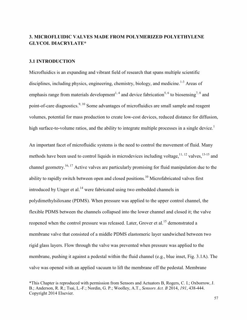
3. MICROFLUIDIC VALVES MADE FROM POLYMERIZED POLYETHYLENE GLYCOL DIACRYLATE*
3.1 INTRODUCTION
Microfluidics is an expanding and vibrant field of research that spans multiple scientific
disciplines, including physics, engineering, chemistry, biology, and medicine.1-3 Areas of
emphasis range from materials development1, 4 and device fabrication5, 6 to biosensing7, 8 and
point-of-care diagnostics.9, 10 Some advantages of microfluidics are small sample and reagent
volumes, potential for mass production to create low-cost devices, reduced distance for diffusion,
high surface-to-volume ratios, and the ability to integrate multiple processes in a single device.1
An important facet of microfluidic systems is the need to control the movement of fluid. Many
methods have been used to control liquids in microdevices including voltage,11, 12 valves,13-15 and
channel geometry.16, 17 Active valves are particularly promising for fluid manipulation due to the
ability to rapidly switch between open and closed positions.10 Microfabricated valves first
introduced by Unger et al.14 were fabricated using two embedded channels in
polydimethylsiloxane (PDMS). When pressure was applied to the upper control channel, the
flexible PDMS between the channels collapsed into the lower channel and closed it; the valve
reopened when the control pressure was released. Later, Grover et al.15 demonstrated a
membrane valve that consisted of a middle PDMS elastomeric layer sandwiched between two
rigid glass layers. Flow through the valve was prevented when pressure was applied to the
membrane, pushing it against a pedestal within the fluid channel (e.g., blue inset, Fig. 3.1A). The
valve was opened with an applied vacuum to lift the membrane off the pedestal. Membrane
*This Chapter is reproduced with permission from Sensors and Actuators B, Rogers, C. I.; Oxborrow, J. B.; Anderson, R. R.; Tsai, L.-F.; Nordin, G. P.; Woolley, A.T., Sensors Act. B 2014, 191, 438-444. Copyright 2014 Elsevier.
57
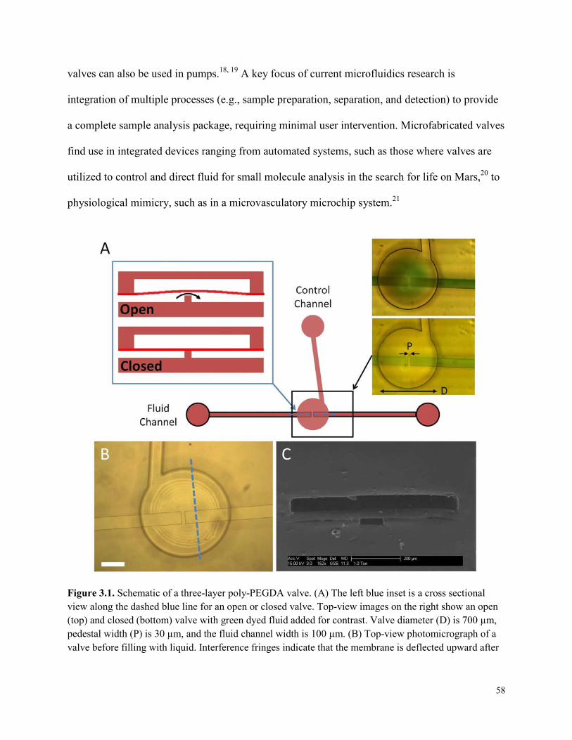
valves can also be used in pumps.18, 19 A key focus of current microfluidics research is
integration of multiple processes (e.g., sample preparation, separation, and detection) to provide
a complete sample analysis package, requiring minimal user intervention. Microfabricated valves
find use in integrated devices ranging from automated systems, such as those where valves are
utilized to control and direct fluid for small molecule analysis in the search for life on Mars,20 to
physiological mimicry, such as in a microvasculatory microchip system.21
Figure 3.1. Schematic of a three-layer poly-PEGDA valve. (A) The left blue inset is a cross sectional view along the dashed blue line for an open or closed valve. Top-view images on the right show an open (top) and closed (bottom) valve with green dyed fluid added for contrast. Valve diameter (D) is 700 µm, pedestal width (P) is 30 µm, and the fluid channel width is 100 µm. (B) Top-view photomicrograph of a valve before filling with liquid. Interference fringes indicate that the membrane is deflected upward after
58

the final bonding step. White scale bar is 200 µm. (C) SEM of a three-layer valve device cross-section along the dashed blue line in (B).
Ideally, valves should have a small volume (< 1 nL), be non-adsorptive, resist swelling, and be
easily fabricated. PDMS is a common valve material because it is easy to mold; however, it is
prone to nonspecific adsorption of proteins and permeation of hydrophobic molecules,22 which is
problematic for bioanalytical applications and nonideal for valves. In response to this
disadvantage, other materials (fluoroelastomers23-25 and a thermoplastic elastomer26) have been
explored as valve membranes in conjunction with rigid fluidic substrates of cyclic olefin
copolymer, poly(methyl methacrylate), or glass. Fluoroelastomers, although resistant to
nonspecific adsorption, are normally opaque and difficult to bond. Thermoplastic elastomers,
although an improvement over PDMS, are still prone to nonspecific adsorption without chemical
modification.27 Polycarbonate, a non-elastomeric polymer, has been used as a valve membrane in
a genetic sensor for tuberculosis; in this setup a solenoid mechanically forced the valve closed.28
More recently, Chen et al.29 demonstrated a pneumatically actuated polystyrene valve for oral
fluid analysis. However, polycarbonate and polystyrene are both prone to nonspecific adsorption
and require large valve areas (>3 mm2) that lead to greater dead volumes that limit device
miniaturization. Polymerized polyethylene glycol diacrylate (poly-PEGDA), another non-
elastomeric polymer, is innately resistant to nonspecific adsorption and small molecule
permeation.22 Although this polymer has a higher elastic modulus (>0.1 GPa)30, 31 than
elastomers, its non-adsorptive nature makes it attractive as a material for monolithic membrane
valves.
In this chapter, I demonstrate for the first time the construction of all-poly-PEGDA membrane
valves for microfluidics. These valves have an 8× smaller area footprint (0.38 mm2) than
59
previously demonstrated non-elastomeric (and typically adsorptive) membrane valves. The
valves are actuated via standard pressurized control, but do not require an elastomeric membrane
material. I have evaluated several different valve designs, including rectangular and circular
geometries. Moreover, I have characterized the temporal response and flow performance of these
poly-PEGDA valves over a range of pressures and number of actuations.
3.2 MATERIALS AND METHODS
3.2.1 Reagents and Materials
Azobisisobutyronitrile (AIBN), polyethylene glycol diacrylate (PEGDA, M.W. 258), and 2,2'-
dimethoxy-2-phenylacetophenone (DMPA) were purchased from Sigma Aldrich (Milwaukee,
WI). Phosphate buffered saline (PBS, 10x) was obtained from Fisher Scientific (Pittsburgh, PA)
and diluted to 1x by adding deionized (DI) water (18.3 MΩ) from a Barnstead EASYpure
UV/UF compact reagent grade water system. Perfluorosilane, (tridecafluoro-1,1,2,2-
tetrahydrooctyl)-1-trichlorosilane, was purchased from UCT Specialties (Bristol, PA). SU8
photoresist (2025 and 2050) was obtained from Microchem (Newton, MA).
3.2.2 Device Fabrication
Thermally initiated prepolymer solutions were prepared by mixing 0.01 % w/w AIBN in
PEGDA. Photoinitiated prepolymer solutions were prepared by combining 0.015 % w/w DMPA
with PEGDA. Solutions were vortexed for 15 s, sonicated for 15 min, and subsequently
refrigerated until use.
Poly-PEGDA valves were fabricated in three general processes: thermal polymerization of
control and fluidic layers, photoinitiated polymerization of the membrane layer, and final device
assembly and bonding (Fig. 3.2). The molds for thermal polymerization were formed using a
60

clean silicon wafer (Fig. 3.2A) on which SU8 features (~80 µm thick for the control layer and
~30 µm thick for the fluidic layer) had been photolithographically patterned (Fig. 3.2B).22 The
mold was placed inside a glass container containing one drop of perfluorosilane, which began to
evaporate when heated to 70°C.32 The perfluorosilane was vapor deposited onto the surface for
10 min to ease polymer removal from the mold. Poly-PEGDA spacers (~500 µm) were used to
define the mold height (Fig. 3.2C), and a 3.5 in glass wafer was used as a cover (Fig. 3.2D).
Prepolymer containing AIBN was then introduced into the cavity (Fig. 3.2E), and the entire mold
was placed into an oven at 80°C for 1-2 h until polymerization was complete (Fig. 3.2F). The
glass cover slide was carefully removed to avoid breaking the wafer (Fig. 3.2G), and the
polymerized layers were subsequently removed, diced, and cleaned with acetone and 2-propanol
(Fig. 3.2H).
Membrane fabrication was accomplished in a similar fashion, but photopolymerization was used.
A clean glass slide was placed on a silicon wafer (Fig. 3.2A), and Mylar spacers (42 µm) were
used to define the mold height (Fig. 3.2C). A glass slide was placed on top (Fig. 3.2D), and 70
µL of prepolymer containing DMPA was introduced into the mold cavity (Fig. 3.2E). UV
exposure at 365 nm (560 mJ/cm2) for 110 s was used to polymerize the membrane (Fig. 3.2F).
The top surface of the membrane was exposed by removing the glass slide (Fig. 3.2G)
immediately before bonding to the control layer (Fig. 3.2I). A clamp was used to hold the layers
in contact during two subsequent UV exposures at 365 nm: the first was at 1.84 J/cm2 for 6 min
in a Karl Suss mask aligner and the second was a 12 J/cm2 exposure for 4 min using a
Spectroline SB-100PR UV lamp. Once these layers were bonded, input/output holes were laser
cut for the fluid channel, and the bonded control/membrane layer was removed from the glass
slide and rinsed with 2-propanol (Fig. 3.2J). The control/membrane layer was then aligned to the
61

fluid channel layer and clamped together (Fig. 3.2K). Vacuum was applied to the
control/membrane layer during alignment and bonding (see Fig. 3.3) to prevent the membrane
from being polymerized to the pedestal during the final bonding step. A 42 J/cm2 UV exposure
for 14 min using the Spectroline UV lamp was used to bond the fluid layer and form the
completed device (Fig. 3.2L).
Figure 3.2. Overview of poly-PEGDA valve fabrication. The top box demonstrates fabrication of the polymerized control (top), membrane (middle), and fluidic (bottom) layers. Final assembly is shown in the bottom box. (A) Clean silicon wafers. (B) SU8 patterns define features. (C) Spacers define poly-PEGDA thickness. (D) Glass wafer forms top of mold. (E) Prepolymer is introduced. (F) Polymerization of poly-PEGDA. (G) Glass cover wafer is removed. (H) Finished poly-PEGDA is removed, diced, and
62

cleaned; an input hole is cut into the control layer. (I) The just-released top surface of the membrane layer (G, middle) is bonded to the control layer (H, top). (J) The bonded control and membrane layers are removed and (K) bonded under vacuum to the fluidic layer using UV light, (L) resulting in a completed valve device.
Figure 3.3. Vacuum clamp for bonding. (A) Side-view image of vacuum clamp, which is made up of four layers (PMMA, PDMS, glass, and PMMA). The poly-PEGDA layers to be bonded are placed in between the PDMS and the glass. (B) Top-view photograph of the vacuum clamp. Vacuum from the tubing at the left is routed through a drilled hole in the PMMA and a hole through the PDMS.
Several different valve geometries were explored. Rectangular valves (700 µm x 600 µm) with 5,
15, and 30 µm pedestals were fabricated, as were circular valves with a 350 µm radius and 5, 15,
30, and 125 µm pedestal widths). The width of the fluid channels in the circular valves was 100
µm (see Fig. 3.1); the fluid channel width in the rectangular valves expanded from 100 µm to
600 µm to match the valve dimensions. Channel depths in these devices ranged between 25-35
µm, membranes were ~40 µm thick, and the control channel height was 55-80 µm.
63
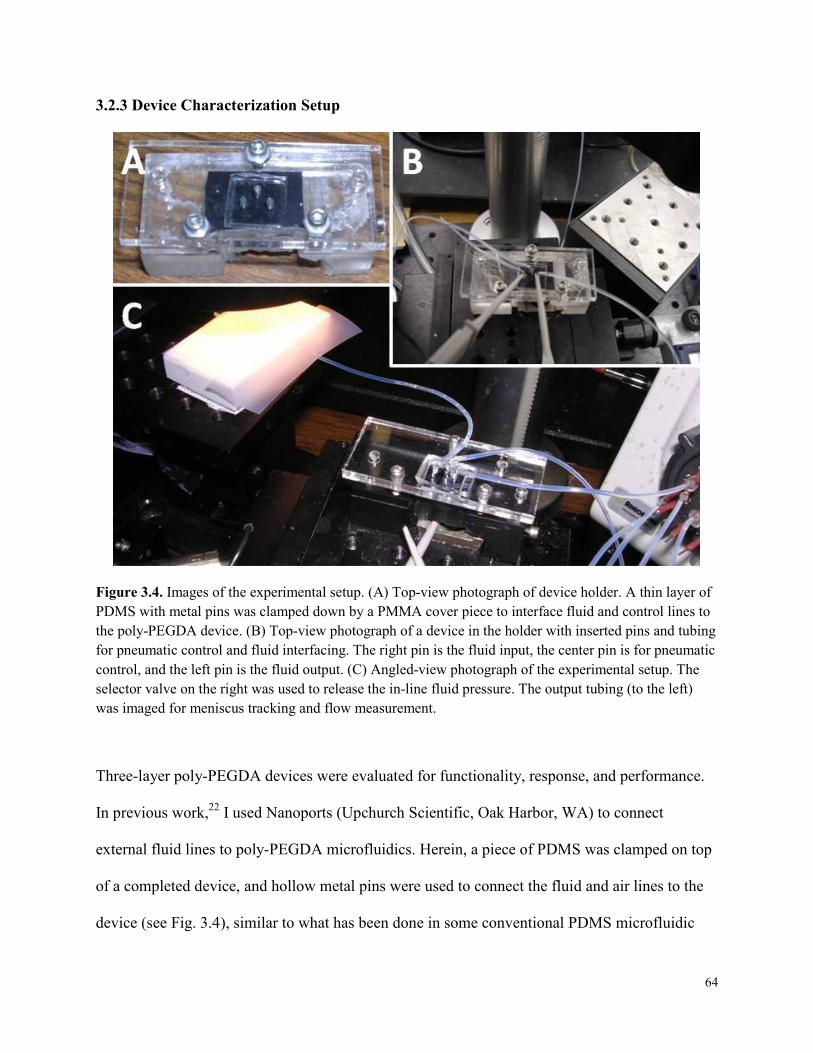
3.2.3 Device Characterization Setup
Figure 3.4. Images of the experimental setup. (A) Top-view photograph of device holder. A thin layer of PDMS with metal pins was clamped down by a PMMA cover piece to interface fluid and control lines to the poly-PEGDA device. (B) Top-view photograph of a device in the holder with inserted pins and tubing for pneumatic control and fluid interfacing. The right pin is the fluid input, the center pin is for pneumatic control, and the left pin is the fluid output. (C) Angled-view photograph of the experimental setup. The selector valve on the right was used to release the in-line fluid pressure. The output tubing (to the left) was imaged for meniscus tracking and flow measurement.
Three-layer poly-PEGDA devices were evaluated for functionality, response, and performance.
In previous work,22 I used Nanoports (Upchurch Scientific, Oak Harbor, WA) to connect
external fluid lines to poly-PEGDA microfluidics. Herein, a piece of PDMS was clamped on top
of a completed device, and hollow metal pins were used to connect the fluid and air lines to the
device (see Fig. 3.4), similar to what has been done in some conventional PDMS microfluidic
64
devices.33, 34 A syringe pump with an inline pressure sensor (Honeywell 24PCFFA6G) was used
to supply fluid to the valve. Regulated, pressurized air with an inline pressure sensor (Honeywell
24PCFFH6G) provided pressure to the control layer. Solenoid valves (Clippard EVO-3M-24)
were used to switch control layer pressure for valve actuation. Valves were evaluated by
comparing the fluid pressure required for flow to commence at a given control pressure. Video
was recorded of meniscus movement in the output tubing and processed using custom LabView
code to determine linear flow velocity, which was then converted to volumetric flow rate. When
fluid flow through the valve was >0.02 µL/min (0.2% of the syringe pump driven 10 µL/min
flow rate), the valve was considered to be open. The Young’s modulus for poly-PEGDA was
calculated from the pressure required to deflect a circular membrane a known distance using
Eq. 3.1 for linear deflection (up to ½ membrane thickness) where P is the applied pressure (Pa),
E is the elastic modulus (Pa), r is the membrane radius (m), h is the membrane thickness (m), ν is
the Poisson’s ratio, and y is the deflection (m) at the membrane center.35
𝑃𝑃𝑟𝑟4
𝐸𝐸ℎ4=
16𝑦𝑦3(1 − 𝜈𝜈2)ℎ
+7 − 𝜈𝜈
3(1 − 𝜈𝜈)𝑦𝑦ℎ3
(3.1)
Water contact angles were measured using a ramé-hart Goniometer (model 100) with 10 µL
water droplets.
The temporal response of valves was measured using a high-speed camera (Photron FASTCAM
SA3) and using color change associated with deflection. A valve actuation rate of 1 Hz with a
30% duty cycle and 207 kPa control pressure was used to evaluate the fall (closure) and rise
(open) time of valves. The rise time was given by the time required for the valve position to go
from 10-90% of its range of motion, and the fall time was determined from the time required for
the valve position to drop from 90-10% of its motion range.
65
Valve performance was evaluated over a range of control pressures (0-207 kPa) and as a function
of number of actuations. PBS (~250 µL) was flowed through the fluid layer of each device
before evaluating valves. Control and fluid pressures were raised incrementally from lower to
higher (0, 70, 148, and 207 kPa). Each valve was actuated at 1 Hz and a 50% duty cycle in
increments of 500 for initial testing, and larger increments (up to 100,000) for long-term testing.
Each valve was retested over the same range of pressures after each series of actuations. Circular
valves with both 15 and 30 µm pedestal widths were used in duty cycle tests.
3.3 RESULTS AND DISCUSSION
3.3.1 Device Characterization Results
Figure 3.1 shows an overview of monolithic membrane valves fabricated entirely from poly-
PEGDA. Applied pressure is used to close the valve, preventing fluid from flowing through (Fig.
3.1A), and the valve is opened by releasing the control pressure and allowing fluid pressure to
deflect the membrane up, resuming flow. Top-view images of the valve with green colored dye
in the fluid channel demonstrate the opening and closure of a valve with a 700 µm diameter and
a 30 µm pedestal (Fig. 3.1A - right images). The membrane is deflected up during fabrication to
prevent bonding to the valve seat (Fig. 3.1B). An SEM image shows a cross-sectional cut
through a poly-PEGDA valve (Fig. 3.1C), illustrating the three-layer fabrication with the deeper
control layer channel on top, the poly-PEGDA membrane in the middle, and the shallower fluid
channel on the bottom. If a Poisson ratio of 0.35 (similar to that of PMMA36) is assumed, the
resulting elastic modulus for poly-PEGDA is determined to be ~0.1 GPa based on membrane
deflection under applied pressure. Although this Young’s modulus is too high to allow poly-
PEGDA to form self-collapsible valves similar to PDMS, which has an elastic modulus ranging
between 0.05-4 MPa (the number varies by formula),37 the elastic modulus allows for utilization
66
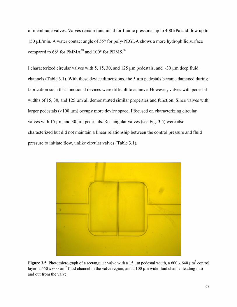
of membrane valves. Valves remain functional for fluidic pressures up to 400 kPa and flow up to
150 µL/min. A water contact angle of 55° for poly-PEGDA shows a more hydrophilic surface
compared to 68° for PMMA38 and 100° for PDMS.39
I characterized circular valves with 5, 15, 30, and 125 µm pedestals, and ~30 µm deep fluid
channels (Table 3.1). With these device dimensions, the 5 µm pedestals became damaged during
fabrication such that functional devices were difficult to achieve. However, valves with pedestal
widths of 15, 30, and 125 µm all demonstrated similar properties and function. Since valves with
larger pedestals (>100 µm) occupy more device space, I focused on characterizing circular
valves with 15 µm and 30 µm pedestals. Rectangular valves (see Fig. 3.5) were also
characterized but did not maintain a linear relationship between the control pressure and fluid
pressure to initiate flow, unlike circular valves (Table 3.1).
Figure 3.5. Photomicrograph of a rectangular valve with a 15 µm pedestal width, a 600 x 640 µm2 control layer, a 550 x 600 µm2 fluid channel in the valve region, and a 100 µm wide fluid channel leading into and out from the valve.
67
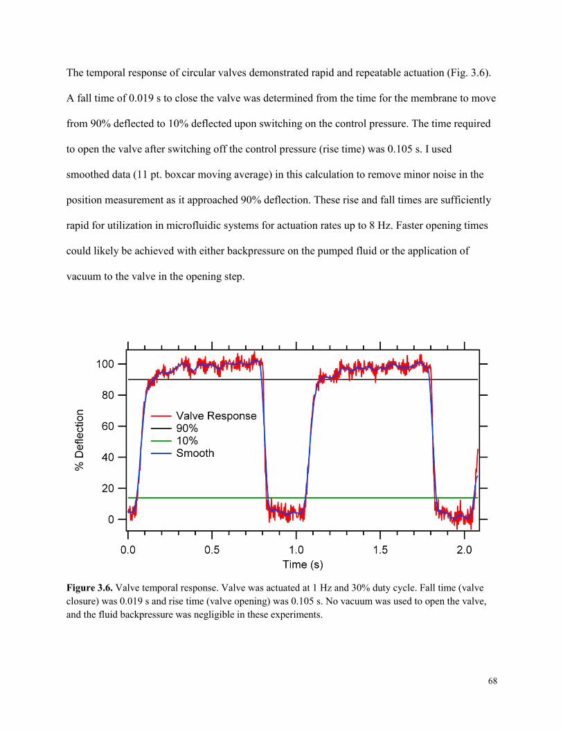
The temporal response of circular valves demonstrated rapid and repeatable actuation (Fig. 3.6).
A fall time of 0.019 s to close the valve was determined from the time for the membrane to move
from 90% deflected to 10% deflected upon switching on the control pressure. The time required
to open the valve after switching off the control pressure (rise time) was 0.105 s. I used
smoothed data (11 pt. boxcar moving average) in this calculation to remove minor noise in the
position measurement as it approached 90% deflection. These rise and fall times are sufficiently
rapid for utilization in microfluidic systems for actuation rates up to 8 Hz. Faster opening times
could likely be achieved with either backpressure on the pumped fluid or the application of
vacuum to the valve in the opening step.
Figure 3.6. Valve temporal response. Valve was actuated at 1 Hz and 30% duty cycle. Fall time (valve closure) was 0.019 s and rise time (valve opening) was 0.105 s. No vacuum was used to open the valve, and the fluid backpressure was negligible in these experiments.
68
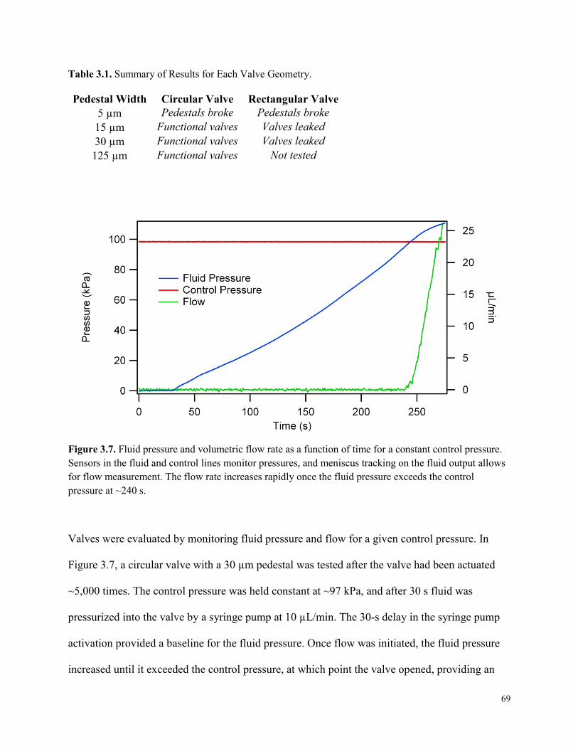
Table 3.1. Summary of Results for Each Valve Geometry.
Pedestal Width Circular Valve Rectangular Valve 5 µm Pedestals broke Pedestals broke 15 µm Functional valves Valves leaked 30 µm Functional valves Valves leaked 125 µm Functional valves Not tested
Figure 3.7. Fluid pressure and volumetric flow rate as a function of time for a constant control pressure. Sensors in the fluid and control lines monitor pressures, and meniscus tracking on the fluid output allows for flow measurement. The flow rate increases rapidly once the fluid pressure exceeds the control pressure at ~240 s.
Valves were evaluated by monitoring fluid pressure and flow for a given control pressure. In
Figure 3.7, a circular valve with a 30 µm pedestal was tested after the valve had been actuated
~5,000 times. The control pressure was held constant at ~97 kPa, and after 30 s fluid was
pressurized into the valve by a syringe pump at 10 µL/min. The 30-s delay in the syringe pump
activation provided a baseline for the fluid pressure. Once flow was initiated, the fluid pressure
increased until it exceeded the control pressure, at which point the valve opened, providing an
69

outlet for the pressure and resulting in flow that rapidly increased towards the pump rate.
Monitoring of fluid and control pressures as well as meniscus movement, was used in evaluating
more than 40 different valves, all of which demonstrated similar behavior. Similar tests were
done multiple times for each valve geometry and pedestal width across a range of pressures and a
number of valve actuations. The relationship between the control pressure and the fluid pressure
at which flow commenced was determined in multiple devices and after various numbers of
actuations. Rearranging Eq. 3.1 for P gives Eq. 3.2 which provides a relationship between
applied pressure and membrane deflection.
𝑃𝑃 =𝐸𝐸ℎ𝑦𝑦(𝜈𝜈2 − 6𝜈𝜈 − 7)𝑦𝑦2 − 16ℎ2
3𝑟𝑟4(𝜈𝜈2 − 1) (3.2)
Figure 3.8. Calculated (line) and experimentally measured (circles) deflection via applied pressure, for a 45 µm thick circular membrane with an elastic modulus of 0.13 GPa, a 350 µm radius, and a Poisson’s ratio of 0.35. Calculated data are from Eq. 3.2. Very low pressure (~9 kPa) is required for significant membrane deflection (>2 µm).
70
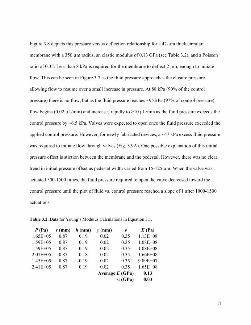
Figure 3.8 depicts this pressure versus deflection relationship for a 42-µm thick circular
membrane with a 350 µm radius, an elastic modulus of 0.13 GPa (see Table 3.2), and a Poisson
ratio of 0.35. Less than 8 kPa is required for the membrane to deflect 2 µm, enough to initiate
flow. This can be seen in Figure 3.7 as the fluid pressure approaches the closure pressure
allowing flow to resume over a small increase in pressure. At 88 kPa (90% of the control
pressure) there is no flow, but as the fluid pressure reaches ~95 kPa (97% of control pressure)
flow begins (0.02 µL/min) and increases rapidly to >10 µL/min as the fluid pressure exceeds the
control pressure by ~6.5 kPa. Valves were expected to open once the fluid pressure exceeded the
applied control pressure. However, for newly fabricated devices, a ~47 kPa excess fluid pressure
was required to initiate flow through valves (Fig. 3.9A). One possible explanation of this initial
pressure offset is stiction between the membrane and the pedestal. However, there was no clear
trend in initial pressure offset as pedestal width varied from 15-125 µm. When the valve was
actuated 500-1500 times, the fluid pressure required to open the valve decreased toward the
control pressure until the plot of fluid vs. control pressure reached a slope of 1 after 1000-1500
actuations.
Table 3.2. Data for Young’s Modulus Calculations in Equation 3.1.
P (Pa) r (mm) h (mm) y (mm) ν E (Pa) 1.65E+05 0.87 0.19 0.02 0.35 1.13E+08 1.59E+05 0.87 0.19 0.02 0.35 1.08E+08 1.59E+05 0.87 0.19 0.02 0.35 1.08E+08 2.07E+05 0.87 0.18 0.02 0.35 1.66E+08 1.45E+05 0.87 0.19 0.02 0.35 9.89E+07 2.41E+05 0.87 0.19 0.02 0.35 1.65E+08
Average E (GPa) 0.13
σ (GPa) 0.03
71
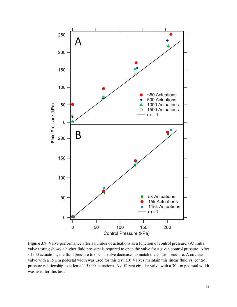
Figure 3.9. Valve performance after a number of actuations as a function of control pressure. (A) Initial valve testing shows a higher fluid pressure is required to open the valve for a given control pressure. After ~1500 actuations, the fluid pressure to open a valve decreases to match the control pressure. A circular valve with a 15 µm pedestal width was used for this test. (B) Valves maintain this linear fluid vs. control pressure relationship to at least 115,000 actuations. A different circular valve with a 30 µm pedestal width was used for this test.
72
Realignment of polymer chains in the device after multiple valve actuations40 could increase the
elasticity of the membrane, thereby making it easier to close. I further evaluated valves for long-
term robustness after very large numbers of actuations (Fig. 3.9B). After 5,000, 15,000, and even
115,000 actuations, the fluid vs. control pressure plot maintained a linear relationship with a
slope of 1, thus demonstrating considerable repeatability and potential for long-term use. Since
1000-1500 actuations were needed for valves to show the expected fluid vs. control pressure
relationship, the valves were preconditioned by performing 1500 actuations before use. Several
different valve designs were evaluated. Rectangular valves with 5, 15, and 30 µm pedestals were
tested. As with circular valves, rectangular valves with 5 µm pedestals were easily damaged
during fabrication. Unlike in circular valves (Figure 3.1), the fluid channel was widened in
rectangular valves to match the control layer design (Fig. 3.5). Rectangular valves did not follow
the linear fluid vs. control pressure relationship observed for circular valves in Figure 3.9. In
addition, the rectangular valve designs were not as effective as circular ones in valve closure at
low control pressures (<70 kPa). The better performance of the circular valves is likely due to the
larger surface area of the valve seat in contact with the membrane, which helps the membrane to
remain planar in the closed state. In contrast, the valve seat contact area with the membrane is
limited to the pedestal only in the rectangular valve design, so the membrane may deflect
partially into the fluid layer.
3.3.2 Device Prospects
Three-layer poly-PEGDA valves have reliable fabrication, fast response times, and robustness
over a large number of actuations. Valves with pedestal widths down to 15 µm have been
successfully made and operated. Possible improvements to these valves include smaller
diameters (<200 µm) and fluid channel widths (<50 µm), and thinner membranes (<20 µm), all
73

of which would further reduce dead volume and improve performance. With combined
application of control pressure and vacuum to control lines and appropriate device layouts, arrays
of these poly-PEGDA valves have potential for application as peristaltic pumps.18, 19 Poly-
PEGDA valve integration with functional or sensing components in other materials, such as
silicon or glass, is also attractive. Finally, the fabrication of embedded electrodes into devices
would enable conductivity or impedance detection, as well as valve closure determination.
Poly-PEGDA valves with their intrinsic resistance to nonspecific adsorption are ideally suited for
biomolecular and protein assays. One example would be the analysis of Tau protein in
cerebrospinal fluid for brain trauma diagnosis41, 42 via an on-chip microdialysis system43 that
extracts small volumes of cerebrospinal fluid, which could then be fluorescently labeled and
purified on-chip44 for subsequent electrophoretic separation and detection. Similarly, thymidine
kinase I in blood serum, which shows promise in diagnosis of hematological cancers,45 could be
captured on-chip using immobilized antibodies,46 and then reacted with a fluorescently labeled
secondary antibody for detection using laser induced fluorescence.47 A final example is the
quantitative analysis of pre-term birth biomarkers in blood serum48, 49 utilizing poly-PEGDA
valves to control sample introduction and pumping for secondary flow required for nanospray
mass spectrometry.50 In these examples, a non-adsorptive device material would enable more of
the analyte of interest to be available for detection and provide symmetrical separation peaks.
3.4 CONCLUSIONS
Poly-PEGDA with inherent nonspecific adhesion resistance properties has been used to form
microfluidic valves. Multiple device geometries were tested; a circular design had a linear fluid
versus control pressure plot over different pedestal widths. A valve opening time of ~100 ms and
74
a closure time of ~20 ms offer valve operation as fast as 8 Hz with potential for further
improvement. A number of replicate measurements after a series of actuations and over a range
of pressures demonstrated the functionality and robustness of these poly-PEGDA valves.
The multi-layer fabrication method developed here for valves can be adapted for on-chip
pumping, which could aid in the integration of automated on-chip sample preparation with
electrophoretic separation. Such pumps could also provide a mechanism for solution mixing, or
find use in a closed system where small-volume specimens could be recirculated over a sensor,
improving sampling. Finally, attachment of these valve systems to silicon or glass devices could
be explored to enable interfacing with micro- and nano-sensors such as microcantilevers, silicon
ring resonators, nanowires, etc.
3.5 REFERENCES
(1) Nge, P. N.; Rogers, C. I.; Woolley, A. T. Chem. Rev. 2013, 113, 2550-2583. (2) Kovarik, M. L.; Ornoff, D. M.; Melvin, A. T.; Dobes, N. C.; Wang, Y.; Dickinson, A. J.;
Gach, P. C.; Shah, P. K.; Allbritton, N. L. Anal. Chem. 2013, 85, 451-472. (3) Arora, A.; Simone, G.; Salieb-Beugelaar, G. B.; Kim, J. T.; Manz, A. Anal. Chem. 2010,
82, 4830-4847. (4) van Midwoud, P. M.; Janse, A.; Merema, M. T.; Groothuis, G. M. M.; Verpoorte, E.
Anal. Chem. 2012, 84, 3938-3944. (5) Abgrall, P.; Gué, A.-M. J. Micromech. Microeng. 2007, 17, R15-R49. (6) Yang, S.; DeVoe, D. L. Microfluidic Diagnostics: Methods and Protocols; Humana
Press: New York City, NY, 2013; Vol. 949, 115-123. (7) Trzebinski, J.; Sharma, S.; Radomska-Botelho Moniz, A.; Michelakis, K.; Zhang, Y.;
Cass, A. E. G. Lab Chip 2012, 12, 348-352. (8) Rivet, C.; Lee, H.; Hirsch, A.; Hamilton, S.; Lu, H. Chem. Eng. Sci. 2011, 66, 1490-1507. (9) Chin, C. D.; Linder, V.; Sia, S. K. Lab Chip 2012, 12, 2118-2134. (10) Gervais, L.; de Rooij, N.; Delamarche, E. Adv. Mater. 2011, 23, H151-176. (11) Mainz, E. R.; Gunasekara, D. B.; Caruso, G.; Jensen, D. T.; Hulvey, M. K.; Fracassi da
Silva, J. A.; Metto, E. C.; Culbertson, A. H.; Culbertson, C. T.; Lunte, S. M. Anal. Methods 2012, 4, 414-420.
(12) Jin, S.; Anderson, G. J.; Kennedy, R. T. Anal. Chem. 2013, 85, 6073-6079. (13) Kim, J.; Kang, M.; Jensen, E. C.; Mathies, R. A. Anal. Chem. 2012, 84, 2067-2071. (14) Unger, M. A.; Chou, H.-P.; Thorsen, T.; Scherer, A.; Quake, S. R. Science 2000, 288,
113-116.
75
(15) Grover, W. H.; Skelley, A. M.; Liu, C. N.; Lagally, E. T.; Mathies, R. A. Sens. Actuators, B 2003, 89, 315-323.
(16) Mohammed, M. I.; Desmulliez, M. P. Y. Microsyst. Technol. 2013, 19, 809-818. (17) Au, A. K.; Lai, H.; Utela, B. R.; Folch, A. Micromachines 2011, 2, 179-220. (18) Grover, W. H.; Mathies, R. A. Lab Chip 2005, 5, 1033-1040. (19) Stockton, A. M.; Mora, M. F.; Cable, M. L.; Willis, P. A. Sens. Actuators, B 2013, 177,
668-675. (20) Kim, J.; Jensen, E. C.; Stockton, A. M.; Mathies, R. A. Anal. Chem. 2013, 85, 7682-
7688. (21) Schimek, K.; Busek, M.; Brincker, S.; Groth, B.; Hoffmann, S.; Lauster, R.; Lindner, G.;
Lorenz, A.; Menzel, U.; Sonntag, F.; Walles, H.; Marx, U.; Horland, R. Lab Chip 2013, 13, 3588-3598.
(22) Rogers, C. I.; Pagaduan, J. V.; Nordin, G. P.; Woolley, A. T. Anal. Chem. 2011, 83, 6418-6425.
(23) Willis, P. A.; Greer, F.; Lee, M. C.; Smith, J. A.; White, V. E.; Grunthaner, F. J.; Sprague, J. J.; Rolland, J. P. Lab Chip 2008, 8, 1024-1026.
(24) Ogilvie, I. R. G.; Sieben, V. J.; Cortese, B.; Mowlem, M. C.; Morgan, H. Lab Chip 2011, 11, 2455-2459.
(25) Huang, S.; He, Q.; Chen, H.; Huang, J. Microfluid. Nanofluid. 2013, 14, 329-335. (26) Rupp, J.; Schmidt, M.; Münch, S.; Cavalar, M.; Steller, U.; Steigert, J.; Stumber, M.;
Dorrer, C.; Rothacher, P.; Zengerle, R.; Daub, M. Lab Chip 2012, 12, 1384-1388. (27) Pan, T.; Fiorini, G. S.; Chiu, D. T.; Woolley, A. T. Electrophoresis 2007, 28, 2904-2911. (28) Wang, H.; Chen, H.-W.; Hupert, M. L.; Chen, P.-C.; Datta, P.; Pittman, T. L.; Goettert,
J.; Murphy, M. C.; Williams, D.; Barany, F.; Soper, S. A. Angew. Chem. 2012, 124, 4425-4429.
(29) Chen, Z.; Abrams, W. R.; Geva, E.; de Dood, C. J.; González, J. M.; Tanke, H. J.; Niedbala, R. S.; Zhou, P.; Malamud, D.; Corstjens, P. L. A. M. BioMed. Res. Int. 2013, 2013, 543294.
(30) Kim, P.; Jeong, H. E.; Khademhosseini, A.; Suh, K. Y. Lab Chip 2006, 6, 1432-1437. (31) Rogers, C. I.; Pagaduan, J. V.; Nordin, G. P.; Woolley, A. T., Orlando, FL, March 11-15,
2012; Pittcon Conference and Expo. (32) Lee, J. K.; Kung, M. C.; Kung, H. H.; Mockros, L. F. ASAIO J. 2008, 54, 390-395. (33) Balagaddé, F. K.; You, L.; Hansen, C. L.; Arnold, F. H.; Quake, S. R. Science 2005, 309,
137-140. (34) Ren, L.; Wang, J.-C.; Liu, W.; Tu, Q.; Liu, R.; Wang, X.; Xu, J.; Wang, Y.; Zhang, Y.;
Li, L.; Wang, J. Biosens. Bioelectron. 2012, 35, 147-154. (35) Kovacs, G. T. A. Micromachined Transducers Sourcebook; McGraw-Hill: New York,
1998, 250. (36) Goswami, A.; Umarji, A. M.; Madras, G. Polym. Adv. Technol. 2012, 23, 1604-1611. (37) Fuard, D.; Tzvetkova-Chevolleau, T.; Decossas, S.; Tracqui, P.; Schiavone, P.
Microelectron. Eng. 2008, 85, 1289-1293. (38) Ma, Y.; Cao, X.; Feng, X.; Ma, Y.; Zou, H. Polymer 2007, 48, 7455-7460. (39) Lawton, R. A.; Price, C. R.; Runge, A. F.; Doherty III, W. J.; Saavedra, S. S. Colloids
Surf., A 2005, 253, 213-215. (40) McKeen, L. W. The Effect of Creep and Other Time Related Factors on Plastics and
Elastomers, 2nd ed.; Elsevier Inc.: Burlington, MA, 2009.
76
(41) Süssmuth, S. D.; Reiber, H.; Tumani, H. Neurosci. Lett. 2001, 300, 95-98. (42) Franz, G.; Beer, R.; Kampfl, A.; Engelhardt, K.; Schmutzhard, E.; Ulmer, H.;
Deisenhammer, F. Neurology 2003, 60, 1457-1461. (43) Huynh, B. H.; Fogarty, B. A.; Nandi, P.; Lunte, S. M. J. Pharm. Biomed. Anal. 2006, 42,
529-534. (44) Nge, P. N.; Pagaduan, J. V.; Yu, M.; Woolley, A. T. J. Chromatogr. A 2012, 1261, 129-
135. (45) Alegre, M. M.; Robison, R. A.; O'Neill, K. L. Cancer Clin. Oncol. 2013, 2, 159-167. (46) Yang, W.; Yu, M.; Sun, X.; Woolley, A. T. Lab Chip 2010, 10, 2527-2533. (47) Salehi-Reyhani, A.; Kaplinsky, J.; Burgin, E.; Novakova, M.; deMello, A. J.; Templer, R.
H.; Parker, P.; Neil, M. A. A.; Ces, O.; French, P.; Willison, K. R.; Klug, D. Lab Chip 2011, 11, 1256-1261.
(48) Vance, C. J.; Esplin, M. S.; Hamblin, S.; Graves, S. W. Am. J. Obstet. Gynecol. 2006, 195, 1407-1414.
(49) Esplin, M. S.; Merrell, K.; Goldenberg, R.; Lai, Y.; Iams, J. D.; Mercer, B.; Spong, C. Y.; Miodovnik, M.; Simhan, H. N.; van Dorsten, P.; Dombrowski, M. Am. J. Obstet. Gynecol. 2011, 204, 391.e391-391.e398.
(50) Chambers, A. G.; Mellors, J. S.; Henley, W. H.; Ramsey, J. M. Anal. Chem. 2011, 83, 842-849.
77

4. PATTERNED DUAL-SILANE DEPOSITION ON QUARTZ TO ENABLE HYBRID MATERIAL INTEGRATION AND SITE-SPECIFIC FUNCTIONALIZATION
4.1 INTRODUCTION
Microfluidics consist of microfabricated 1–500 µm features that allow for managing femtoliter to
nanoliter fluid movement.1 As channel size decreases, the surface-to-volume ratio increases and
surface chemistry becomes more influential. As microfluidics has focused on biosensing, the
ability to change the available surface chemistry inside microfluidic channels and adapt that
chemistry for better biocompatibility2 and probe attachment (e.g., peptides,3 proteins,4 and
DNA5) has become more important.
Site-specific functionalization is desirable in biosensing because it creates areas of differing
surface chemistries that allow for various applications. Ness et al.6 demonstrated inkjet printing
as a method to attach biotinylated bovine serum albumin to one side of a microcantilever to
generate differential stress when interacting with streptavidin. Sweetman et al.7 showed that
photolithography can be used to pattern areas onto porous silicon with three different silane
pairs. Adaptation of this process for use with quartz, which is transparent down to 185 nm8 and
has low autoflourescence,9 could allow the integration of different materials while providing
regions for further chemical modification via well characterized methods.
Polymerized polyethylene glycol diacrylate (poly-PEGDA) is a nonspecific adsorption resistant
material desirable for utilization with biological samples.10 Poly-PEGDA is optically clear,
resistant to permeation of small molecules, and suitable for use with electrophoresis (see
Chapter 2) and valves (see Chapter 3).10, 11 Bonding poly-PEGDA microfluidics with different
78
substrate materials (e.g., glass, silicon, or electrode-patterned materials) provides broader
application for biosensing and device integration.
Evaluation of dual-silane patterning and poly-PEGDA device bonding to silicon and quartz is
demonstrated in this Chapter. Photolithographic patterning of a silane-functionalized surface
enables area-specific silane removal through HF etching of the exposed regions. This also creates
a clean surface for subsequent deposition of a different, secondary silane on the etched regions.
Dual-silane deposition onto these substrates makes bonding to poly-PEGDA possible through
UV exposure, while providing specific locations for crosslinking desired molecules to the
surface. An amine-reactive fluorescent molecule is utilized to evaluate the dual silane deposition
process on quartz. Preliminary results for site-specific secondary attachment using
glutaraldehyde as a crosslinker and a reactive fluorophore are discussed in this Chapter as well.
4.2 MATERIALS AND METHODS
4.2.1 Reagents and Materials
Nanostrip was acquired from Cyanotek (Fremont, CA) and buffered oxide etchant (BOE,
hydrofluoric acid) was from Transene Company (Danvers, MA). Warning: hydrofluoric acid is
dangerous! Use the proper protective equipment when using! The base/acid solutions were
created by individually diluting hydrochloric acid (EMD Chemicals, Gibbstown, NJ) and sodium
hydroxide (EM Science, Gibbstown, NJ) to 0.1 M in 18.3 MΩ DI water (EASYpure UV/UF).
Dimethyl sulfoxide (DMSO), glutaraldehyde (8% solution in water), fluoresceinamine,
polyethylene glycol diacrylate (PEGDA, 258 Da), 3-(trimethoxysilyl)propyl methacrylate
(TMSPMA), 2,2′-azobis(2-methylpropionitrile) (AIBN), and 2,2'-dimethoxy-2-
phenylacetophenone (DMPA) were purchased through Sigma-Aldrich (Milwaukee, WI).
79
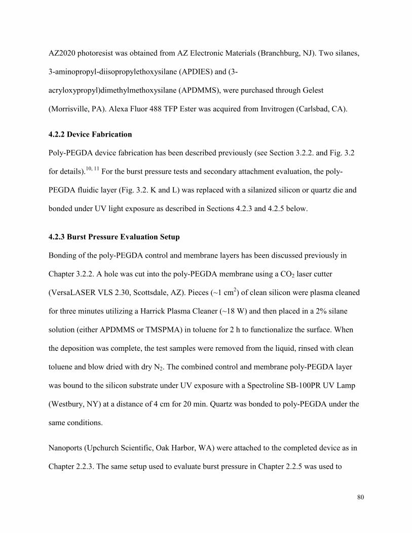
AZ2020 photoresist was obtained from AZ Electronic Materials (Branchburg, NJ). Two silanes,
3-aminopropyl-diisopropylethoxysilane (APDIES) and (3-
acryloxypropyl)dimethylmethoxysilane (APDMMS), were purchased through Gelest
(Morrisville, PA). Alexa Fluor 488 TFP Ester was acquired from Invitrogen (Carlsbad, CA).
4.2.2 Device Fabrication
Poly-PEGDA device fabrication has been described previously (see Section 3.2.2. and Fig. 3.2
for details).10, 11 For the burst pressure tests and secondary attachment evaluation, the poly-
PEGDA fluidic layer (Fig. 3.2. K and L) was replaced with a silanized silicon or quartz die and
bonded under UV light exposure as described in Sections 4.2.3 and 4.2.5 below.
4.2.3 Burst Pressure Evaluation Setup
Bonding of the poly-PEGDA control and membrane layers has been discussed previously in
Chapter 3.2.2. A hole was cut into the poly-PEGDA membrane using a CO2 laser cutter
(VersaLASER VLS 2.30, Scottsdale, AZ). Pieces (~1 cm2) of clean silicon were plasma cleaned
for three minutes utilizing a Harrick Plasma Cleaner (~18 W) and then placed in a 2% silane
solution (either APDMMS or TMSPMA) in toluene for 2 h to functionalize the surface. When
the deposition was complete, the test samples were removed from the liquid, rinsed with clean
toluene and blow dried with dry N2. The combined control and membrane poly-PEGDA layer
was bound to the silicon substrate under UV exposure with a Spectroline SB-100PR UV Lamp
(Westbury, NY) at a distance of 4 cm for 20 min. Quartz was bonded to poly-PEGDA under the
same conditions.
Nanoports (Upchurch Scientific, Oak Harbor, WA) were attached to the completed device as in
Chapter 2.2.3. The same setup used to evaluate burst pressure in Chapter 2.2.5 was used to
80
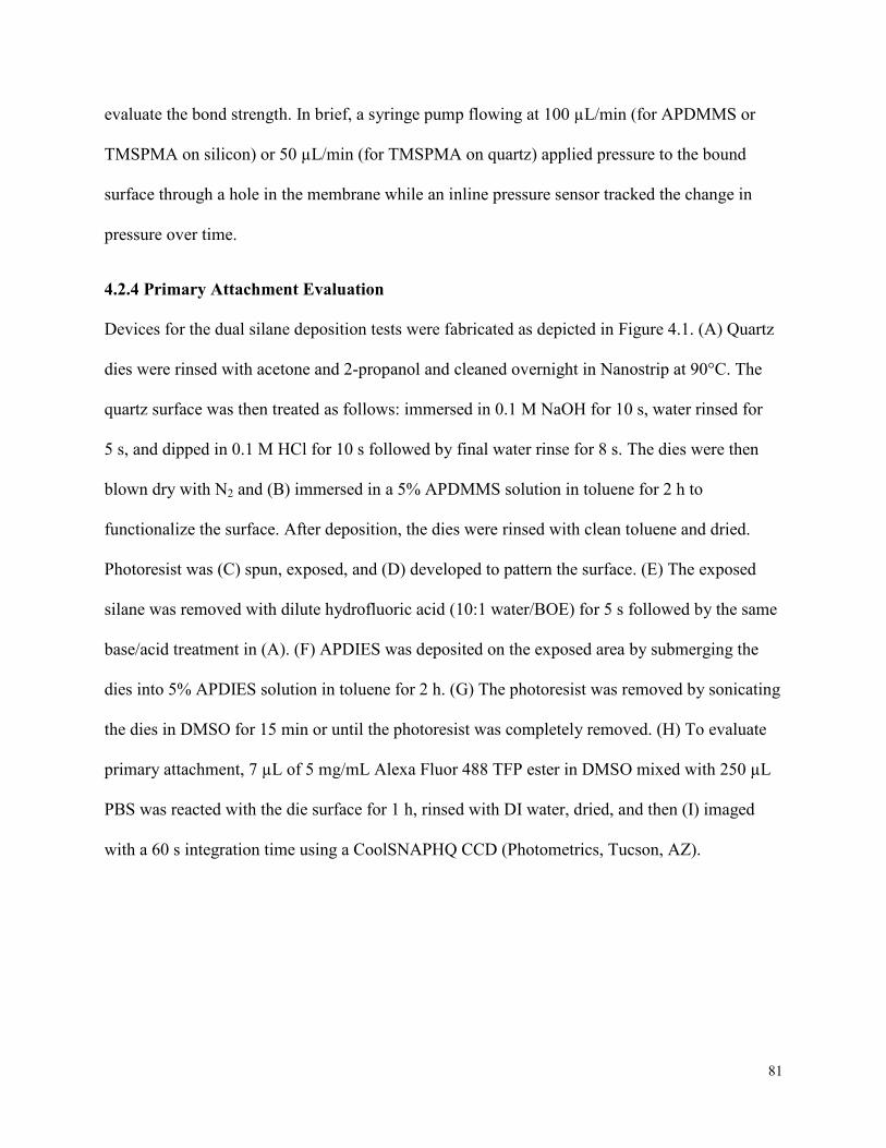
evaluate the bond strength. In brief, a syringe pump flowing at 100 µL/min (for APDMMS or
TMSPMA on silicon) or 50 µL/min (for TMSPMA on quartz) applied pressure to the bound
surface through a hole in the membrane while an inline pressure sensor tracked the change in
pressure over time.
4.2.4 Primary Attachment Evaluation
Devices for the dual silane deposition tests were fabricated as depicted in Figure 4.1. (A) Quartz
dies were rinsed with acetone and 2-propanol and cleaned overnight in Nanostrip at 90°C. The
quartz surface was then treated as follows: immersed in 0.1 M NaOH for 10 s, water rinsed for
5 s, and dipped in 0.1 M HCl for 10 s followed by final water rinse for 8 s. The dies were then
blown dry with N2 and (B) immersed in a 5% APDMMS solution in toluene for 2 h to
functionalize the surface. After deposition, the dies were rinsed with clean toluene and dried.
Photoresist was (C) spun, exposed, and (D) developed to pattern the surface. (E) The exposed
silane was removed with dilute hydrofluoric acid (10:1 water/BOE) for 5 s followed by the same
base/acid treatment in (A). (F) APDIES was deposited on the exposed area by submerging the
dies into 5% APDIES solution in toluene for 2 h. (G) The photoresist was removed by sonicating
the dies in DMSO for 15 min or until the photoresist was completely removed. (H) To evaluate
primary attachment, 7 µL of 5 mg/mL Alexa Fluor 488 TFP ester in DMSO mixed with 250 µL
PBS was reacted with the die surface for 1 h, rinsed with DI water, dried, and then (I) imaged
with a 60 s integration time using a CoolSNAPHQ CCD (Photometrics, Tucson, AZ).
81
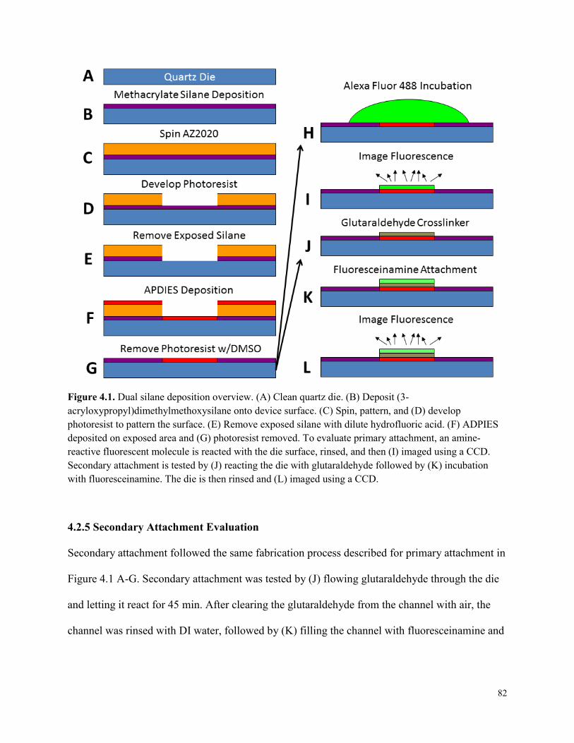
Figure 4.1. Dual silane deposition overview. (A) Clean quartz die. (B) Deposit (3-acryloxypropyl)dimethylmethoxysilane onto device surface. (C) Spin, pattern, and (D) develop photoresist to pattern the surface. (E) Remove exposed silane with dilute hydrofluoric acid. (F) ADPIES deposited on exposed area and (G) photoresist removed. To evaluate primary attachment, an amine-reactive fluorescent molecule is reacted with the die surface, rinsed, and then (I) imaged using a CCD. Secondary attachment is tested by (J) reacting the die with glutaraldehyde followed by (K) incubation with fluoresceinamine. The die is then rinsed and (L) imaged using a CCD.
4.2.5 Secondary Attachment Evaluation
Secondary attachment followed the same fabrication process described for primary attachment in
Figure 4.1 A-G. Secondary attachment was tested by (J) flowing glutaraldehyde through the die
and letting it react for 45 min. After clearing the glutaraldehyde from the channel with air, the
channel was rinsed with DI water, followed by (K) filling the channel with fluoresceinamine and
82
letting it incubate in the channel for 26 h. The poly-PEGDA layers were then removed from the
die, which was then rinsed with DI water, dried, and (L) imaged using a CCD (60 s exposure).
4.3 RESULTS AND DISCUSSION
Figure 4.2. Photograph of poly-PEGDA device bonded to quartz. White scale bar is 250 µm.
Figure 4.2 shows an example of poly-PEGDA microfluidic layers bound to a quartz substrate.
This is a three-layer valve with a fluidic channel etched into the quartz and bonded to a poly-
PEGDA control and membrane layer (See Chapter 3 and Fig. 3.1 for more details).
4.3.1 Burst Pressure Results
The pressure required to separate the bonded layers is proportional to the bond strength between
those layers. As seen in Figure 4.3, pressure slowly built up at the interface until a leak caused
the pressure to drop at ~60 s. The pressure curves for both the monofunctional and trifunctional
83
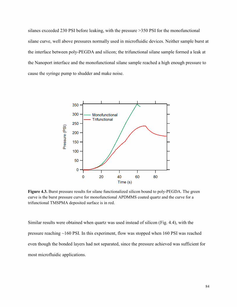
silanes exceeded 230 PSI before leaking, with the pressure >350 PSI for the monofunctional
silane curve, well above pressures normally used in microfluidic devices. Neither sample burst at
the interface between poly-PEGDA and silicon; the trifunctional silane sample formed a leak at
the Nanoport interface and the monofunctional silane sample reached a high enough pressure to
cause the syringe pump to shudder and make noise.
Figure 4.3. Burst pressure results for silane functionalized silicon bound to poly-PEGDA. The green curve is the burst pressure curve for monofunctional APDMMS coated quartz and the curve for a trifunctional TMSPMA deposited surface is in red.
Similar results were obtained when quartz was used instead of silicon (Fig. 4.4), with the
pressure reaching ~160 PSI. In this experiment, flow was stopped when 160 PSI was reached
even though the bonded layers had not separated, since the pressure achieved was sufficient for
most microfluidic applications.
84
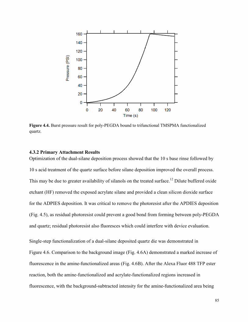
Figure 4.4. Burst pressure result for poly-PEGDA bound to trifunctional TMSPMA functionalized quartz.
4.3.2 Primary Attachment Results Optimization of the dual-silane deposition process showed that the 10 s base rinse followed by
10 s acid treatment of the quartz surface before silane deposition improved the overall process.
This may be due to greater availability of silanols on the treated surface.12 Dilute buffered oxide
etchant (HF) removed the exposed acrylate silane and provided a clean silicon dioxide surface
for the ADPIES deposition. It was critical to remove the photoresist after the APDIES deposition
(Fig. 4.5), as residual photoresist could prevent a good bond from forming between poly-PEGDA
and quartz; residual photoresist also fluoresces which could interfere with device evaluation.
Single-step functionalization of a dual-silane deposited quartz die was demonstrated in
Figure 4.6. Comparison to the background image (Fig. 4.6A) demonstrated a marked increase of
fluorescence in the amine-functionalized areas (Fig. 4.6B). After the Alexa Fluor 488 TFP ester
reaction, both the amine-functionalized and acrylate-functionalized regions increased in
fluorescence, with the background-subtracted intensity for the amine-functionalized area being
85
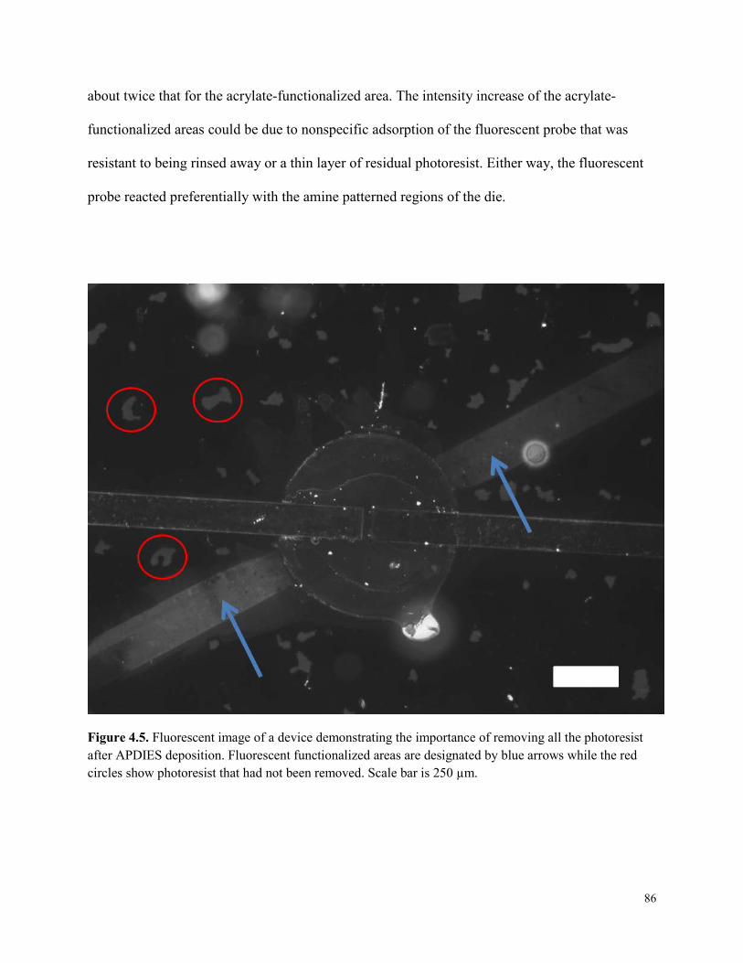
about twice that for the acrylate-functionalized area. The intensity increase of the acrylate-
functionalized areas could be due to nonspecific adsorption of the fluorescent probe that was
resistant to being rinsed away or a thin layer of residual photoresist. Either way, the fluorescent
probe reacted preferentially with the amine patterned regions of the die.
Figure 4.5. Fluorescent image of a device demonstrating the importance of removing all the photoresist after APDIES deposition. Fluorescent functionalized areas are designated by blue arrows while the red circles show photoresist that had not been removed. Scale bar is 250 µm.
86
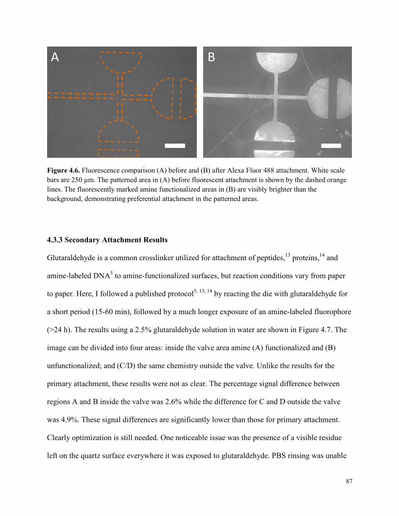
Figure 4.6. Fluorescence comparison (A) before and (B) after Alexa Fluor 488 attachment. White scale bars are 250 µm. The patterned area in (A) before fluorescent attachment is shown by the dashed orange lines. The fluorescently marked amine functionalized areas in (B) are visibly brighter than the background, demonstrating preferential attachment in the patterned areas.
4.3.3 Secondary Attachment Results
Glutaraldehyde is a common crosslinker utilized for attachment of peptides,13 proteins,14 and
amine-labeled DNA5 to amine-functionalized surfaces, but reaction conditions vary from paper
to paper. Here, I followed a published protocol5, 13, 14 by reacting the die with glutaraldehyde for
a short period (15-60 min), followed by a much longer exposure of an amine-labeled fluorophore
(>24 h). The results using a 2.5% glutaraldehyde solution in water are shown in Figure 4.7. The
image can be divided into four areas: inside the valve area amine (A) functionalized and (B)
unfunctionalized; and (C/D) the same chemistry outside the valve. Unlike the results for the
primary attachment, these results were not as clear. The percentage signal difference between
regions A and B inside the valve was 2.6% while the difference for C and D outside the valve
was 4.9%. These signal differences are significantly lower than those for primary attachment.
Clearly optimization is still needed. One noticeable issue was the presence of a visible residue
left on the quartz surface everywhere it was exposed to glutaraldehyde. PBS rinsing was unable
87
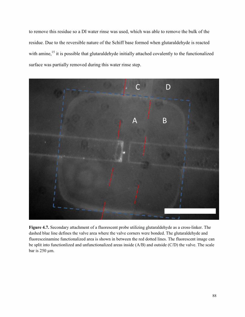
to remove this residue so a DI water rinse was used, which was able to remove the bulk of the
residue. Due to the reversible nature of the Schiff base formed when glutaraldehyde is reacted
with amine,15 it is possible that glutaraldehyde initially attached covalently to the functionalized
surface was partially removed during this water rinse step.
Figure 4.7. Secondary attachment of a fluorescent probe utilizing glutaraldehyde as a cross-linker. The dashed blue line defines the valve area where the valve corners were bonded. The glutaraldehyde and fluoresceinamine functionalized area is shown in between the red dotted lines. The fluorescent image can be split into functionlized and unfunctionalized areas inside (A/B) and outside (C/D) the valve. The scale bar is 250 µm.
88

4.4 CONCLUSIONS
Integration of poly-PEGDA microfluidics with acrylate-silanized silicon and quartz devices with
stability under applied pressures >160 PSI has been demonstrated. Dual silane deposition of
TMSPMA and APDIES through photolithographic patterning provided a method, which not only
enabled poly-PEGDA bonding to quartz but also created regions on the surface readily available
for further chemical modification. Direct reaction of a fluorophore with these amine-
functionalized areas showed that site-specific attachment is possible. Exploration and
optimization using different surface chemistries, such as epoxy and sulfhydryl, would provide
wider application to different surface attachment methods.
Glutaraldehyde, although common in cross-linking, comes with some limitations such as self-
polymerization as the cyclic hemiacetal under acidic pH conditions, which gets worse as the
solution ages.15 Thus, there are potential ways to improve the cross-linking reaction. The
glutaraldehyde solutions in this experiment were around neutral pH; changing to basic pH (9 or
10) could improve the glutaraldehyde attachment yield.16 Furthermore, reaction with
borohydride17 or cyanoborohydride18 to reduce the Schiff base into a secondary amine would
improve the bond stability as well. Another alternative would be to switch to a different amine-
amine coupler, such as NHS-diazirine19 which has an NHS ester for the primary amine
attachment and utilizes UV light exposure to form the secondary amine attachment.
4.5 REFERENCES
(1) Nge, P. N.; Rogers, C. I.; Woolley, A. T. Chem. Rev. 2013, 113, 2550-2583. (2) van Midwoud, P. M.; Janse, A.; Merema, M. T.; Groothuis, G. M. M.; Verpoorte, E.
Anal. Chem. 2012, 84, 3938-3944. (3) Didar, T. F.; Tabrizian, M. Lab Chip 2012, 12, 4363-4371. (4) Chikkaveeraiah, B. V.; Mani, V.; Patel, V.; Gutkind, J. S.; Rusling, J. F. Biosens.
Bioelectron. 2011, 26, 4477-4483.
89

(5) Chatterjee, D.; Mansfield, D. S.; Woolley, A. T. Anal. Methods 2014, 6, 8173-8179. (6) Ness, S. J.; Kim, S.; Woolley, A. T.; Nordin, G. P. Sens. Actuators, B 2012, 161, 80-87. (7) Sweetman, M. J.; Shearer, C. J.; Shapter, J. G.; Voelcker, N. H. Langmuir 2011, 27,
9497-9503. (8) Duffy, D. C.; McDonald, J. C.; Schueller, O. J. A.; Whitesides, G. M. Anal. Chem. 1998,
70, 4974-4984. (9) Pokhriyal, A.; Lu, M.; Chaudhery, V.; Huang, C.-S.; Schulz, S.; Cunningham, B. T. Opt.
Express 2010, 18, 24793-24808. (10) Rogers, C. I.; Pagaduan, J. V.; Nordin, G. P.; Woolley, A. T. Anal. Chem. 2011, 83,
6418-6425. (11) Rogers, C. I.; Oxborrow, J. B.; Anderson, R. R.; Tsai, L. F.; Nordin, G. P.; Woolley, A.
T. Sens. Actuators, B 2014, 191, 438-444. (12) Cypryk, M.; Apeloig, Y. Organometallics 2002, 21, 2165-2175. (13) Xiao, S.-J.; Textor, M.; Spencer, N. D.; Sigrist, H. Langmuir 1998, 14, 5507-5516. (14) Zhang, Y.; Zhang, Y.; Jiang, J.; Li, L.; Yu, C.; Hei, T. Appl. Surf. Sci. 2011, 257, 2712-
2716. (15) Hermanson, G. T. Bioconjugate Techniques, 3rd ed.; Academic Press: Boston, MA,
2013, 275-298. (16) Hermanson, G. T. Bioconjugate Techniques, 3rd ed.; Academic Press: Boston, MA,
2013, 589-740. (17) Ahmed, S. R.; Kelly, A. B.; Barbari, T. A. J. Membr. Sci. 2006, 280, 553-559. (18) Park, M. K.; Kee, J. S.; Quah, J. Y.; Netto, V.; Song, J.; Fang, Q.; La Fosse, E. M.; Lo,
G.-Q. Sens. Actuators, B 2013, 176, 552-559. (19) Gomes, A. F.; Gozzo, F. C. J. Mass Spectrom. 2010, 45, 892-899.
90
5. 3D PRINTED MICROFLUIDIC DEVICES WITH INTEGRATED VALVES*
5.1 INTRODUCTION
Microfluidics1 is a critical technology for an extremely broad range of biomedical applications
including tissue engineering,2, 3 drug discovery,4 point-of-care diagnostics and pathogen
detection in both developed and developing countries,5-8 and cancer screening using approaches
such as cell identification,9 protein,10-13 DNA14 and micro-RNA15, 16 biomarkers. Microfluidic
device prototyping for proof-of-principle demonstration typically utilizes hot embossed or
injection molded plastics1, 17 or polydimethylsiloxane (PDMS).18, 19 In either case, two or more
individually fabricated layers are bonded together to form a completed device. The fabrication
process typically involves cleanroom microfabrication of molds using photolithography for one
or more of the individual layers, followed by molding and release of each layer and then careful
layer alignment and bonding. This sequence of steps can lead to a delay of a week or more
between completing the design of a device and actually having one in hand to test; especially
taking into account the inevitable problems that crop up for various fabrication steps in a
university environment and the turn-around time to design and procure photolithographic masks.
To reduce mask acquisition time, mask writers, such as the Heidelberg DWL-66FS laser
lithography system,20 can be used. Fabrication times range from 2 hours for low resolution masks
(>5 µm) to ~5 days for high resolution masks (>0.6 µm). Inkjet printing on transparencies is
another low cost option for rapid mask printing, taking only a few minutes, but the resolution
isn’t as good (>50 µm).21 Moreover, limited material choices for prototyping microfluidic
systems also hinders their broad development, as problems such as non-specific adsorption that
plague PDMS and other polymers22, 23 prevent many potential applications from being tested.
*This Chapter is reproduced with permission from Biomicrofluidics, Rogers, C. I.; Pagaduan, J. V.; Nordin, G. P.; Woolley, A. T., Biomicrofluidics 2015, 9, 016501. Copyright 2015 AIP Publishing.
91
Of course, once the masks and processes are in place for a given design, it usually takes only
hours to possibly a day or two to produce additional devices of that design. However, initial
microfluidic testing often reveals design or performance deficiencies that necessitate modifying
the design and starting the process over, thereby incurring yet another significant delay.
Numerous cycles around this loop can be required to develop a successful device, which
stretches the development time with a concomitantly large increase in personnel costs. Moreover,
this lengthy cycle time discourages trying new approaches when faced with tight development
deadlines. This is in direct contrast to the “fail fast and often” strategy successfully employed for
web and smartphone application software development where early and rapid user feedback is
used to guide project development throughout the development cycle. By analogy, 3D printing of
microfluidics offers the opportunity to shrink the time from design to first device to an hour or
less because the device is created directly in a single step with no need for layer-by-layer
fabrication and assembly as with PDMS. This completely changes the development landscape by
not only dramatically reducing the opportunity cost of trying new ideas but also permitting a
“fail fast and often” strategy in which early and rapid empirical feedback is used to guide and
accelerate device development. Moreover, 3D printing does not require a cleanroom
environment with its attendant start up investment and ongoing operational costs. In other words,
3D printed microfluidics dramatically lowers the barrier to creating sophisticated microfluidic
devices and offers a true rapid-prototyping ability with its attendant benefits to positively disrupt
microfluidic development cycles.
Unfortunately, this promise in 3D printed microfluidics has not yet been realized, although there
have been a number of efforts in this direction.24 For example, Kitson et al.25-27 demonstrated
fluidic devices 3D printed by extruding plastic through a heated nozzle. However, this
92
fabrication method is inherently unable to produce feature sizes and flow channel dimensions
needed for microfluidic (as opposed to macrofluidic or millifluidic) device fabrication. For the
reported devices, the flow channels had very large cross sections (~4 mm diameter).
A more promising approach for microfluidics is stereolithography in which a vector scanned
laser beam or a stationary image pattern from a projector is used to photopolymerize an
appropriate photosensitive resin layer-by-layer until a full device is completed. For example,
Bhargava et al.28 report a system in which discrete ~1 cm3 3D printed cubes, each with internal
plumbing to perform a specific passive elementary function (such as an L-joint, mixer, T-
junction, XX-junction, etc.), are assembled into more complex fluidic devices in a 3D geometry.
Each cube has standardized fluidic interfaces on 2 or more sides according to the elementary
function performed within the cube. The cubes snap together to create precise cube-to-cube
fluidic connections. While innovative, the overall system size can be comparatively large
depending on how many cubes are needed. Furthermore, since the fluid channel minimum cross
section dimension ranges from 500-1,000 µm, this is more properly termed a millifluidic system.
The cubes themselves are fabricated by a contract manufacturer (FineLine Prototyping, Raleigh,
NC) using a proprietary, commercially available resin with a scanned laser stereolithographic 3D
printer. This approach is appealing in that it is universally available to any customer, but the
large flow channels and system size, and lack of control over resin formulation and, hence,
surface and bulk chemistry can be unnecessarily restrictive for many applications.
Interestingly, another group recently published a paper using the same contract manufacturer,
except their focus is direct fabrication of entire custom microfluidic devices.29 They showed that
flow channels with cross sectional features down to 400 µm were possible. However, this
93
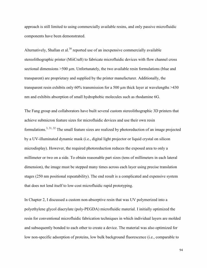
approach is still limited to using commercially available resins, and only passive microfluidic
components have been demonstrated.
Alternatively, Shallan et al.30 reported use of an inexpensive commercially available
stereolithographic printer (MiiCraft) to fabricate microfluidic devices with flow channel cross
sectional dimensions >500 µm. Unfortunately, the two available resin formulations (blue and
transparent) are proprietary and supplied by the printer manufacturer. Additionally, the
transparent resin exhibits only 60% transmission for a 500 µm thick layer at wavelengths >430
nm and exhibits absorption of small hydrophobic molecules such as rhodamine 6G.
The Fang group and collaborators have built several custom stereolithographic 3D printers that
achieve submicron feature sizes for microfluidic devices and use their own resin
formulations.3, 31, 32 The small feature sizes are realized by photoreduction of an image projected
by a UV-illuminated dynamic mask (i.e., digital light projector or liquid crystal on silicon
microdisplay). However, the required photoreduction reduces the exposed area to only a
millimeter or two on a side. To obtain reasonable part sizes (tens of millimeters in each lateral
dimension), the image must be stepped many times across each layer using precise translation
stages (250 nm positional repeatability). The end result is a complicated and expensive system
that does not lend itself to low-cost microfluidic rapid prototyping.
In Chapter 2, I discussed a custom non-absorptive resin that was UV polymerized into a
polyethylene glycol diacrylate (poly-PEGDA) microfluidic material. I initially optimized the
resin for conventional microfluidic fabrication techniques in which individual layers are molded
and subsequently bonded to each other to create a device. The material was also optimized for
low non-specific adsorption of proteins, low bulk background fluorescence (i.e., comparable to
94
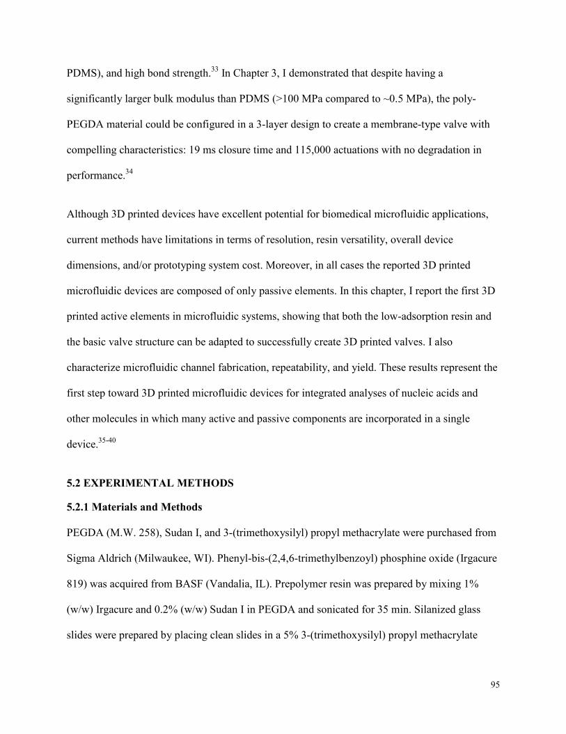
PDMS), and high bond strength.33 In Chapter 3, I demonstrated that despite having a
significantly larger bulk modulus than PDMS (>100 MPa compared to ~0.5 MPa), the poly-
PEGDA material could be configured in a 3-layer design to create a membrane-type valve with
compelling characteristics: 19 ms closure time and 115,000 actuations with no degradation in
performance.34
Although 3D printed devices have excellent potential for biomedical microfluidic applications,
current methods have limitations in terms of resolution, resin versatility, overall device
dimensions, and/or prototyping system cost. Moreover, in all cases the reported 3D printed
microfluidic devices are composed of only passive elements. In this chapter, I report the first 3D
printed active elements in microfluidic systems, showing that both the low-adsorption resin and
the basic valve structure can be adapted to successfully create 3D printed valves. I also
characterize microfluidic channel fabrication, repeatability, and yield. These results represent the
first step toward 3D printed microfluidic devices for integrated analyses of nucleic acids and
other molecules in which many active and passive components are incorporated in a single
device.35-40
5.2 EXPERIMENTAL METHODS
5.2.1 Materials and Methods
PEGDA (M.W. 258), Sudan I, and 3-(trimethoxysilyl) propyl methacrylate were purchased from
Sigma Aldrich (Milwaukee, WI). Phenyl-bis-(2,4,6-trimethylbenzoyl) phosphine oxide (Irgacure
819) was acquired from BASF (Vandalia, IL). Prepolymer resin was prepared by mixing 1%
(w/w) Irgacure and 0.2% (w/w) Sudan I in PEGDA and sonicated for 35 min. Silanized glass
slides were prepared by placing clean slides in a 5% 3-(trimethoxysilyl) propyl methacrylate
95
solution in toluene for 3 h. After deposition, the slides were scribed (to mark the print face),
cleaved, rinsed with clean toluene, blown dry with a nitrogen gun, and stored for later use.
5.2.2 Experimental Setup
I used a B9 Creator 3D printer v1.1 (B9 Creations, Rapid City, SD) to fabricate these devices. To
determine feature size fidelity and device yield, I 3D printed 8 samples, each with an identical set
of horizontal flow channels with different designed cross sections ranging from 300-500 µm
width and 150-250 µm height in 50 µm increments. Vertical flow channels were 3D printed on
one die, but with four different vertical holes for each size from 300-450 µm and eight holes for
500-800 µm (each in 50 µm increments). The cross-sectional dimensions were measured using
digital photographs processed in ImageJ 1.48v.
Figure 5.1. Valve schematic and device image. (A) Top view and (B) side view schematics of test valve design. The control chamber (green) and fluidic chamber (blue) regions are voids in the 3D printed device. The control chamber has 2 access ports to enable it to be drained after printing. Pressure can be applied through both ports to actuate the valve, or one channel can be sealed and pressure applied through the other to actuate the valve. Pressurized membrane (black dotted line) shows valve closure. (C) Photograph of a fabricated valve test device looking through the top surface of the device. The left valve has a 3 mm diameter membrane, while the right valve membrane is 1.5 mm diameter. Dead volume of these valves can be approximated as a cone (volume = 1/3 πr2h) where r is radius of the valve and h is the amount of membrane deflection up into the control chamber. For a control chamber height of 500 µm, the maximum dead volume would be ~1.2 µL for the 3 mm valve and ~0.3 µL for the 1.5 mm valve.
96

Once feasible channel dimensions were determined, these dimensions were then used to create
the channels for the valve design. The valve design, shown in Figures 5.1A and 5.1B, consists of
a membrane suspended over a valve chamber, on the bottom of which are inlet and outlet
openings. When an external pressure source is applied to the control chamber above the
membrane, the membrane is deflected downward until it seals the inlet and outlet openings,
thereby closing the valve. When pressure is released, the membrane returns to its original
position and the valve opens. A photograph of a fabricated test valve device is shown in
Figure 5.1C.
The 3D printing process to fabricate a device with a valve is illustrated schematically in Figure
5.2. In brief, double-sided tape was used to affix a methacrylate silane functionalized glass slide
to the bottom of the build table before calibrating the build table height for the print. After the
resin was introduced into the tray and the projector was focused at the surface of the glass slide,
different images were projected for each layer to polymerize each layer and create the desired 3D
structure. Once the print was completed, unpolymerized resin was then drained from the
structure, resulting in a completed device.
97
Figure 5.2. Fabrication process. (A) An acrylate silane functionalized glass slide is attached to the bottom of the build table. (B) Resin is added to the print tray and the slide is positioned above the bottom window. (C) The projector image is focused on the bottom surface of the glass slide, which (D) polymerizes resin in the exposed region. (E) The projector image is varied layer-by-layer to create the desired 3D structure. (F) When the device is pulled from the bath after all layers are exposed, the channels contain unpolymerized resin, which must be drained from the structure, resulting in (G) a finished device.
5.2.3 Membrane Thickness
Membrane thickness as a function of exposure time was evaluated by measuring a 2 mm
diameter circular single layer membrane (~50 µm) suspended between two 250 µm high
chambers. Exposure times between 2 s and 10 s were tested. Membrane thicknesses were
measured from digital photographs using ImageJ.
98
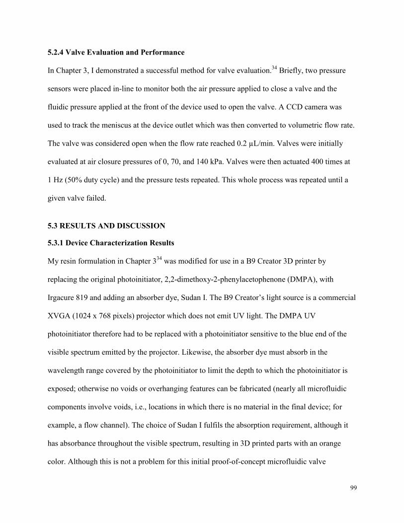
5.2.4 Valve Evaluation and Performance
In Chapter 3, I demonstrated a successful method for valve evaluation.34 Briefly, two pressure
sensors were placed in-line to monitor both the air pressure applied to close a valve and the
fluidic pressure applied at the front of the device used to open the valve. A CCD camera was
used to track the meniscus at the device outlet which was then converted to volumetric flow rate.
The valve was considered open when the flow rate reached 0.2 µL/min. Valves were initially
evaluated at air closure pressures of 0, 70, and 140 kPa. Valves were then actuated 400 times at
1 Hz (50% duty cycle) and the pressure tests repeated. This whole process was repeated until a
given valve failed.
5.3 RESULTS AND DISCUSSION
5.3.1 Device Characterization Results
My resin formulation in Chapter 334 was modified for use in a B9 Creator 3D printer by
replacing the original photoinitiator, 2,2-dimethoxy-2-phenylacetophenone (DMPA), with
Irgacure 819 and adding an absorber dye, Sudan I. The B9 Creator’s light source is a commercial
XVGA (1024 x 768 pixels) projector which does not emit UV light. The DMPA UV
photoinitiator therefore had to be replaced with a photoinitiator sensitive to the blue end of the
visible spectrum emitted by the projector. Likewise, the absorber dye must absorb in the
wavelength range covered by the photoinitiator to limit the depth to which the photoinitiator is
exposed; otherwise no voids or overhanging features can be fabricated (nearly all microfluidic
components involve voids, i.e., locations in which there is no material in the final device; for
example, a flow channel). The choice of Sudan I fulfils the absorption requirement, although it
has absorbance throughout the visible spectrum, resulting in 3D printed parts with an orange
color. Although this is not a problem for this initial proof-of-concept microfluidic valve
99
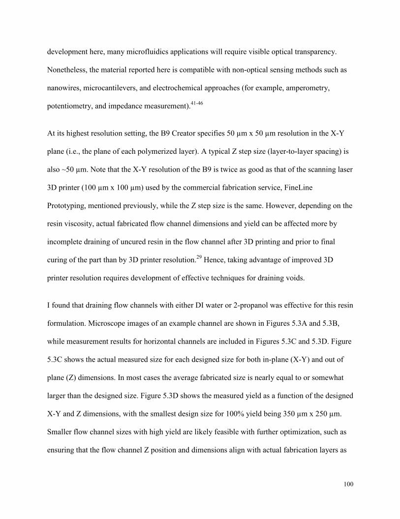
development here, many microfluidics applications will require visible optical transparency.
Nonetheless, the material reported here is compatible with non-optical sensing methods such as
nanowires, microcantilevers, and electrochemical approaches (for example, amperometry,
potentiometry, and impedance measurement).41-46
At its highest resolution setting, the B9 Creator specifies 50 µm x 50 µm resolution in the X-Y
plane (i.e., the plane of each polymerized layer). A typical Z step size (layer-to-layer spacing) is
also ~50 µm. Note that the X-Y resolution of the B9 is twice as good as that of the scanning laser
3D printer (100 µm x 100 µm) used by the commercial fabrication service, FineLine
Prototyping, mentioned previously, while the Z step size is the same. However, depending on the
resin viscosity, actual fabricated flow channel dimensions and yield can be affected more by
incomplete draining of uncured resin in the flow channel after 3D printing and prior to final
curing of the part than by 3D printer resolution.29 Hence, taking advantage of improved 3D
printer resolution requires development of effective techniques for draining voids.
I found that draining flow channels with either DI water or 2-propanol was effective for this resin
formulation. Microscope images of an example channel are shown in Figures 5.3A and 5.3B,
while measurement results for horizontal channels are included in Figures 5.3C and 5.3D. Figure
5.3C shows the actual measured size for each designed size for both in-plane (X-Y) and out of
plane (Z) dimensions. In most cases the average fabricated size is nearly equal to or somewhat
larger than the designed size. Figure 5.3D shows the measured yield as a function of the designed
X-Y and Z dimensions, with the smallest design size for 100% yield being 350 µm x 250 µm.
Smaller flow channel sizes with high yield are likely feasible with further optimization, such as
ensuring that the flow channel Z position and dimensions align with actual fabrication layers as
100
determined by the software that slices a 3D computer-aided design (CAD) file to prepare it for
3D printing.
Figure 5.3. Horizontal channel fabrication, repeatability, and yield. (A) Top view and (B) side view of a flow channel with designed cross section size of 350 μm x 250 μm. The measured cross section of the fabricated flow channel is 316 μm x 217 μm. (C) Actual (measured) flow channel size as a function of the designed size (error bars show standard deviation based on measurement of 8 samples). (D) Yield as a function of the designed X-Y and Z dimension sizes for 8 devices where yield represents the frequency of a successfully printed open channel.
The microscope image shown in Figure 5.4A shows a typical example of a vertical cylindrical
channel. Measurement results for channels designed with diameters ranging from 300 µm to 800
µm are shown in Figure 5.4B. The smallest vertical channel successfully printed with 100%
101
yield had a 350 µm designed diameter and 210 µm average measured diameter. As seen in Fig.
5.4B, the as-printed diameters of the holes are smaller than the designed size.
Figure 5.4. Vertical cylindrical channel fabrication, repeatability, and yield. (A) Top view of a designed 650 μm cylindrical channel. The measured diameter of the channel is 606 μm. (B) Actual (measured) cylindrical channel size as a function of the designed size. Successfully printed open channels (yield) as a function of the designed cylinder diameters. Error bars denote standard deviation based on measurement of four channels (300-450 μm holes) or eight channels (500-800 μm holes).
5.3.2 Membrane Thickness
The as-fabricated membrane thickness has a critical effect on valve performance and lifetime.
Figure 5.5 shows the measured membrane thickness as a function of layer exposure time. As
expected, longer layer exposure time results in greater membrane thickness because the valve
chamber behind the membrane is filled with unexposed resin. The longer the exposure, the
deeper into this region the polymerization front advances. Note that this not only makes the
membrane thicker (and therefore stiffer), but also decreases the distance the membrane must
deflect to seal the inlet and outlet openings. My experiments indicate an exposure time in the
range of 5.0 to 5.5 s/layer works well. Exposures less than 3 s failed to successfully print due to
weak bonding between print layers, and at 3 s the print layers were damaged easily. On the other
102
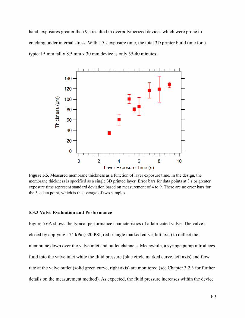
hand, exposures greater than 9 s resulted in overpolymerized devices which were prone to
cracking under internal stress. With a 5 s exposure time, the total 3D printer build time for a
typical 5 mm tall x 8.5 mm x 30 mm device is only 35-40 minutes.
Figure 5.5. Measured membrane thickness as a function of layer exposure time. In the design, the membrane thickness is specified as a single 3D printed layer. Error bars for data points at 3 s or greater exposure time represent standard deviation based on measurement of 4 to 9. There are no error bars for the 3 s data point, which is the average of two samples.
5.3.3 Valve Evaluation and Performance
Figure 5.6A shows the typical performance characteristics of a fabricated valve. The valve is
closed by applying ~74 kPa (~20 PSI, red triangle marked curve, left axis) to deflect the
membrane down over the valve inlet and outlet channels. Meanwhile, a syringe pump introduces
fluid into the valve inlet while the fluid pressure (blue circle marked curve, left axis) and flow
rate at the valve outlet (solid green curve, right axis) are monitored (see Chapter 3.2.3 for further
details on the measurement method). As expected, the fluid pressure increases within the device
103
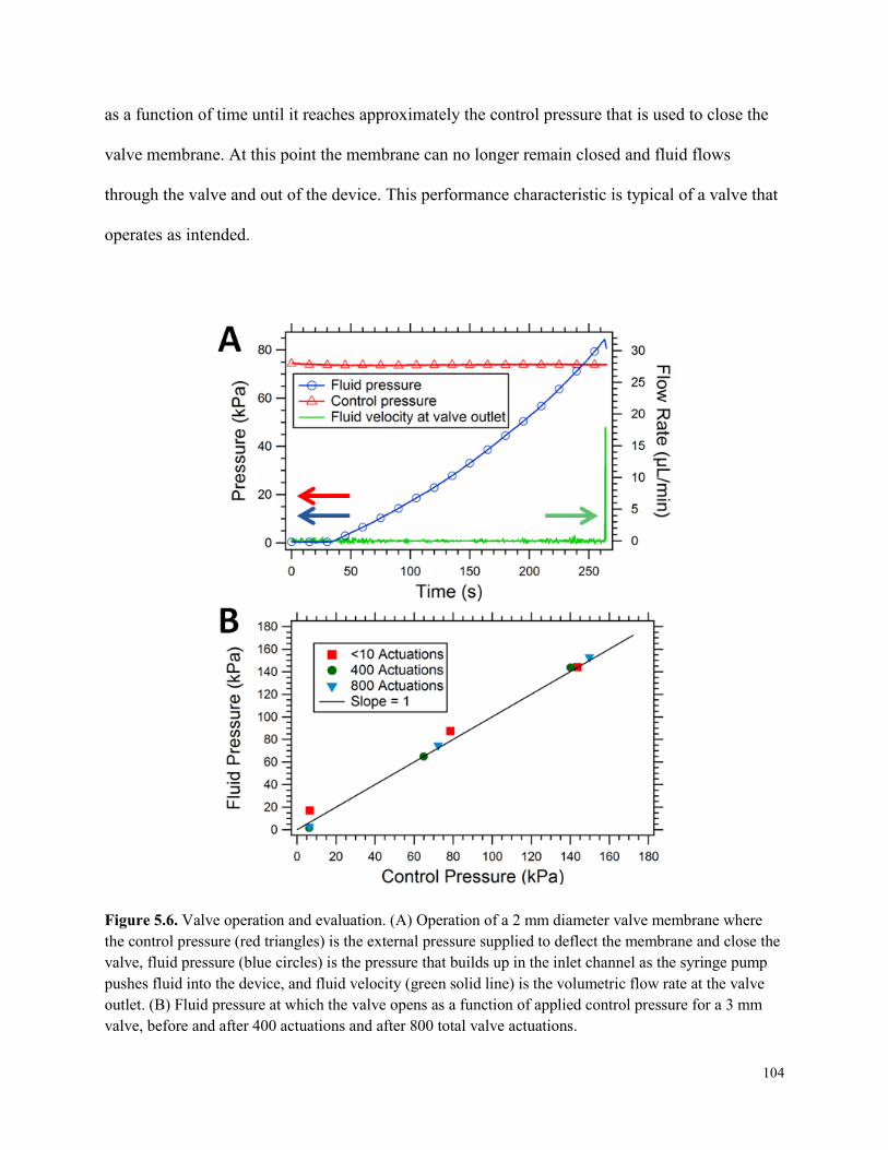
as a function of time until it reaches approximately the control pressure that is used to close the
valve membrane. At this point the membrane can no longer remain closed and fluid flows
through the valve and out of the device. This performance characteristic is typical of a valve that
operates as intended.
Figure 5.6. Valve operation and evaluation. (A) Operation of a 2 mm diameter valve membrane where the control pressure (red triangles) is the external pressure supplied to deflect the membrane and close the valve, fluid pressure (blue circles) is the pressure that builds up in the inlet channel as the syringe pump pushes fluid into the device, and fluid velocity (green solid line) is the volumetric flow rate at the valve outlet. (B) Fluid pressure at which the valve opens as a function of applied control pressure for a 3 mm valve, before and after 400 actuations and after 800 total valve actuations.
104
Figure 5.6B shows the fluid pressure at which flow through the device occurs as a function of the
control pressure applied to close the membrane for an as-fabricated valve and the same valve
after it has undergone 400 and 800 open/close actuation cycles. Each data point represents one
measurement similar to what is shown in Figure 6A. The data shown in Figure 6B is
representative of what was measured for several devices. The data indicate that when the fluid
pressure rises above the control pressure, the valve opens, as expected. Note that there is
essentially no difference in valve performance before and after 400 or 800 actuations. I find that
the valve membrane typically breaks sometime after 800 actuations. Given my earlier results in
Chapter 3.3.1 for poly-PEGDA microfluidic valves where over 100,000 actuations resulted in
little change in performance,34 I am confident that lifetimes of 3D printed microfluidic valves
can be dramatically increased.
5.4 CONCLUSIONS
I have successfully demonstrated readily fabricated 3D printed microfluidic channels with
valves, within devices that take less than one hour to print. Moreover, the yield for horizontal
flow channels with cross sections as small as 350 µm x 250 µm is 100%. Vertical channels were
3D printed successfully as small as 350 µm diameter with 100% yield as well. Undoubtedly,
flow channel size can be decreased through further optimization. Valve diameters as small as
2 mm have been shown to be viable and behave as expected with opening fluid pressure
approximately equal to the control air pressure applied to close the valve. Switching to a higher
resolution printer will likely decrease channel dimensions and valve sizes, while further
processing steps such as post-print thermal or UV curing may improve the lifetime of the valves.
105

Owing to the absorber in my initial resin formulation, the fabricated devices are not fully
transparent in the visible wavelength region, and may also have bulk fluorescence. Although
these current devices may be incompatible with biosensing based on optical absorbance or
fluorescence measurements, ongoing future work to evaluate resin formulations with alternate
photoinitiators and absorbers will address these issues. Development of a non-proprietary resin
will allow for greater flexibility in modifying polymer properties such as surface chemistry to
enable subsequent modification for application in immunoassays or nucleic acid assays, for
example. Furthermore, the ability to print these devices directly onto glass surfaces opens up the
potential for direct integration with a range of substrates (e.g., glass, silicon, or materials with
patterned electrodes) which could dramatically lower the barrier-to-entry to explore lab-on-a-
chip biosensors, thereby expanding the lab-on-a-chip research and development community and
enabling accelerated biomedical sensor innovation.
5.5 REFERENCES
(1) Nge, P. N.; Rogers, C. I.; Woolley, A. T. Chem. Rev. 2013, 113, 2550-2583. (2) Khademhosseini, A.; Langer, R.; Borenstein, J.; Vacanti, J. P. Proc. Natl. Acad. Sci.
U.S.A. 2006, 103, 2480-2487. (3) Xia, C.; Fang, N. X. Biomed. Microdevices 2009, 11, 1309-1315. (4) Neuži, P.; Giselbrecht, S.; Länge, K.; Huang, T. J.; Manz, A. Nat. Rev. Drug Discovery
2012, 11, 620-632. (5) Chin, C. D.; Laksanasopin, T.; Cheung, Y. K.; Steinmiller, D.; Linder, V.; Parsa, H.;
Wang, J.; Moore, H.; Rouse, R.; Umviligihozo, G.; Karita, E.; Mwambarangwe, L.; Braunstein, S. L.; van de Wijgert, J.; Sahabo, R.; Justman, J. E.; El-Sadr, W.; Sia, S. K. Nat. Med. 2011, 17, 1015-1019.
(6) Foudeh, A. M.; Fatanat Didar, T.; Veres, T.; Tabrizian, M. Lab Chip 2012, 12, 3249-3266.
(7) Mulvaney, S. P.; Myers, K. M.; Sheehan, P. E.; Whitman, L. J. Biosens. Bioelectron. 2009, 24, 1109-1115.
(8) Sin, M. L.; Mach, K. E.; Wong, P. K.; Liao, J. C. Expert Rev. Mol. Diagn. 2014, 14, 225-244.
(9) Saliba, A.-E.; Saias, L.; Psychari, E.; Minc, N.; Simon, D.; Bidard, F.-C.; Mathiot, C.; Pierga, J.-Y.; Fraisier, V.; Salamero, J.; Saada, V.; Farace, F.; Vielh, P.; Malaquin, L.; Viovy, J.-L. Proc. Natl. Acad. Sci. 2010, 107, 14524-14529.
106
(10) Chikkaveeraiah, B. V.; Mani, V.; Patel, V.; Gutkind, J. S.; Rusling, J. F. Biosens. Bioelectron. 2011, 26, 4477-4483.
(11) Hu, M.; Yan, J.; He, Y.; Lu, H.; Weng, L.; Song, S.; Fan, C.; Wang, L. ACS Nano 2010, 4, 488-494.
(12) Malhotra, R.; Patel, V.; Chikkaveeraiah, B. V.; Munge, B. S.; Cheong, S. C.; Zain, R. B.; Abraham, M. T.; Dey, D. K.; Gutkind, J. S.; Rusling, J. F. Anal. Chem. 2012, 84, 6249-6255.
(13) Ziober, B. L.; Mauk, M. G.; Falls, E. M.; Chen, Z.; Ziober, A. F.; Bau, H. H. Head & Neck 2007, 30, 111-121.
(14) Mulvaney, S. P.; Cole, C. L.; Kniller, M. D.; Malito, M.; Tamanaha, C. R.; Rife, J. C.; Stanton, M. W.; Whitman, L. J. Biosens. Bioelectron. 2007, 23, 191-200.
(15) Moltzahn, F.; Olshen, A. B.; Baehner, L.; Peek, A.; Fong, L.; Stoppler, H.; Simko, J.; Hilton, J. F.; Carroll, P.; Blelloch, R. Cancer Res. 2011, 71, 550-560.
(16) Vorwerk, S.; Ganter, K.; Cheng, Y.; Hoheisel, J.; Stähler, P. F.; Beier, M. New Biotechnol. 2008, 25, 142-149.
(17) Mei, Q.; Xia, Z.; Xu, F.; Soper, S. A.; Fan, Z. H. Anal. Chem. 2008, 80, 6045-6050. (18) Friend, J.; Yeo, L. Biomicrofluidics 2010, 4, 026502. (19) Sia, S. K.; Whitesides, G. M. Electrophoresis 2003, 24, 3563-3576. (20) http://www.himt.de/index.php/dwl-series-overview.html (21) Duffy, D. C.; McDonald, J. C.; Schueller, O. J. A.; Whitesides, G. M. Anal. Chem. 1998,
70, 4974-4984. (22) Huang, B.; Wu, H. K.; Kim, S.; Zare, R. N. Lab Chip 2005, 5, 1005-1007. (23) Shah, J. J.; Geist, J.; Locascio, L. E.; Gaitan, M.; Rao, M. V.; Vreeland, W. N.
Electrophoresis 2006, 27, 3788-3796. (24) Gross, B. C.; Erkal, J. L.; Lockwood, S. Y.; Chen, C.; Spence, D. M. Anal. Chem. 2014,
86, 3240-3253. (25) Kitson, P. J.; Rosnes, M. H.; Sans, V.; Dragone, V.; Cronin, L. Lab Chip 2012, 12, 3267-
3271. (26) Kitson, P. J.; Symes, M. D.; Dragone, V.; Cronin, L. Chem. Sci. 2013, 4, 3099-3103. (27) Symes, M. D.; Kitson, P. J.; Yan, J.; Richmond, C. J.; Cooper, G. J. T.; Bowman, R. W.;
Vilbrandt, T.; Cronin, L. Nat. Chem. 2012, 4, 349-354. (28) Bhargava, K. C.; Thompson, B.; Malmstadt, N. Proc. Natl. Acad. Sci. 2014, 111, 15013-
15018. (29) Au, A. K.; Lee, W.; Folch, A. Lab Chip 2014, 14, 1294. (30) Shallan, A. I.; Smejkal, P.; Corban, M.; Guijt, R. M.; Breadmore, M. C. Anal. Chem.
2014, 86, 3124-3130. (31) Sun, C.; Fang, N.; Wu, D. M.; Zhang, X. Sens. Actuators, A 2005, 121, 113-120. (32) Zheng, X.; Deotte, J.; Alonso, M. P.; Farquar, G. R.; Weisgraber, T. H.; Gemberling, S.;
Lee, H.; Fang, N.; Spadaccini, C. M. Rev. Sci. Instrum. 2012, 83, 125001. (33) Rogers, C. I.; Pagaduan, J. V.; Nordin, G. P.; Woolley, A. T. Anal. Chem. 2011, 83,
6418-6425. (34) Rogers, C. I.; Oxborrow, J. B.; Anderson, R. R.; Tsai, L. F.; Nordin, G. P.; Woolley, A.
T. Sens. Actuators, B 2014, 191, 438-444. (35) Crabtree, H. J.; Lauzon, J.; Morrissey, Y.; Taylor, B.; Liang, T.; Johnstone, R.; Stickel,
A.; Manage, D.; Atrazhev, A.; Backhouse, C.; Pilarski, L. Microfluid. Nanofluid. 2012, 13, 383-398.
107
(36) Kim, J.; Jensen, E. C.; Stockton, A. M.; Mathies, R. A. Anal. Chem. 2013, 85, 7682-7688.
(37) Collino, R. R.; Reilly-Shapiro, N.; Foresman, B.; Xu, K.; Utz, M.; Landers, J. P.; Begley, M. R. Lab Chip 2013, 13, 3668-3674.
(38) Godwin, L. A.; Pilkerton, M. E.; Deal, K. S.; Wanders, D.; Judd, R. L.; Easley, C. J. Anal. Chem. 2011, 83, 7166-7172.
(39) Yu, F.; Horowitz, M. A.; Quake, S. R. Lab Chip 2013, 13, 1911-1918. (40) Shackman, J. G.; Reid, K. R.; Dugan, C. E.; Kennedy, R. T. Anal. Bioanal. Chem. 2012,
402, 2797-2803. (41) García, M.; García-Carmona, L.; Escarpa, A. Microfluidic system for enzymeless
electrochemical determination of inulin using catalytically active metal nanowires. Microchim Acta [Online early access]. 10.1007/s00604-014-1384-5 Published Online: http://dx.doi.org/10.1007/s00604-014-1384-5 (accessed 2015/1/19).
(42) McClellan, M. S.; Domier, L. L.; Bailey, R. C. Biosens. Bioelectron. 2012, 31, 388-392. (43) Anderson, R. R.; Hu, W.; Noh, J. W.; Dahlquist, W. C.; Ness, S. J.; Gustafson, T. M.;
Richards, D. C.; Kim, S.; Mazzeo, B. A.; Woolley, A. T.; Nordin, G. P. Lab Chip 2011, 11, 2088-2096.
(44) Ness, S. J.; Anderson, R. R.; Hu, W. S.; Richards, D. C.; Oxborrow, J.; Gustafson, T.; Tsai, B.; Kim, S.; Mazzeo, B.; Woolley, A.; Nordin, G. P. IEEE Sens. J. 2013, 13, 959 - 968
(45) Anderson, K. B.; Lockwood, S. Y.; Martin, R. S.; Spence, D. M. Anal. Chem. 2013, 85, 5622-5626.
(46) Vázquez, M.; Frankenfeld, C.; Coltro, W. K. T.; Carrilho, E.; Diamond, D.; Lunte, S. M. Analyst 2010, 135, 96-103.
108
6. CONCLUSIONS AND FUTURE WORK
6.1 CONCLUSIONS
6.1.1 Single-Monomer Formulation of Polymerized Polyethylene Glycol Diacrylate as a Nonadsorptive Material for Microfluidics
In Chapter 2, I demonstrated that polyethylene glycol diacrylate (PEGDA) can be polymerized
via UV exposure and utilized as a microfluidic substrate. Water stability, respectable bond
strength, and good optical clarity were shown. Diffusion of small hydrophobic molecules into the
bulk material was compared between poly-PEGDA and polydimethylsiloxane (PDMS), with
poly-PEGDA showing excellent resistance to permeation compared to PDMS. Nonspecific
protein adsorption over a range of protein concentrations was compared for both materials, with
poly-PEGDA demonstrating lower nonspecific adsorption than PDMS. Under exposure of a low
protein concentration sustained over time, poly-PEGDA demonstrated greater resistance to
surface fouling than PDMS. Poly-PEGDA made from purified resin also showed a low intrinsic
fluorescent background similar to that of PDMS. Electrophoretic separations of amino acids and
proteins utilizing poly-PEGDA as a microchip capillary electrophoresis substrate showed
symmetrical, well-resolved peaks with good theoretical plate counts. These separations, along
with resistance to nonspecific adsorption and low background fluorescence, demonstrated the
potential benefits of using poly-PEGDA over PDMS as a microfluidic substrate for biological
sample analysis.
6.1.2 Microfluidic Valves Made from Polymerized Polyethylene Glycol Diacrylate
Three-layer microfluidic membrane valves made with poly-PEGDA were demonstrated in
Chapter 3. Valves were bonded with an applied vacuum to prevent the membrane from sticking
closed during UV exposure. Multiple valve geometries were evaluated, but the 700-µm-diameter
109

circular design yielded the best results: a linear, slope of one, fluid versus control pressure curve
for pedestal widths of 15-125 µm. Pressure for deflection experiments demonstrated that these
valves require very little pressure (~9 kPa) to generate membrane deflections ˃2 µm. Valve
opening and closure response times were evaluated using periodic applied pressure and pressure
release, resulting in a rise time for valve opening of ~100 ms and a fall time for valve closure of
~20 ms. Valves could be operated as fast as 8 Hz with potential for faster valve opening times.
Valve response measurements with fewer than 1000 actuations showed that the fluid pressure
required to open the valve and initiate flow was about 50 kPa higher than the control pressure.
As the valve was actuated more, the fluid pressure required to open the valve dropped to be the
same as the pressure applied for valve closure. Poly-PEGDA valves were shown to be robust,
remaining functional for up to 115,000 actuations.
6.1.3 Patterned Dual-Silane Deposition on Quartz to Enable Hybrid Material Integration and Site-Specific Functionalization
In Chapter 4, I demonstrated heterogeneous device formation by integrating poly-PEGDA
microfluidics with different substrates via acrylate-silane deposition. Good bond strengths in
these hybrid devices were shown, with burst pressures ˃160 PSI for both silicon and quartz
bound to poly-PEGDA. Photolithographic patterning of the initial silane, followed by HF etching
and subsequent deposition of a secondary silane, allowed for device bonding and site-specific
chemical modification. Removing photoresist before poly-PEGDA layer attachment was crucial,
as the fluorescence from the resist could interfere with fluorescence evaluation of chemical
modified surfaces. Site-specific functionalization was evaluated by reacting amine-silanized
areas directly with a fluorophore. Initial results with secondary attachment utilizing
glutaraldehyde were also shown but needed more optimization to achieve better fluorescent
probe attachment.
110
6.1.4 3D Printed Microfluidic Devices with Integrated Valves
The poly-PEGDA prepolymer formula from Chapters 2-4 was adapted for utilization in 3D
printing. Chapter 5 contains the first demonstration of 3D printed valves in microfluidic systems.
Devices up to 5-mm-tall, containing 3D printed microfluidic channels with valves ≥2 mm
diameter, were printed in under an hour. Horizontal flow channels with cross sections down to
350 µm x 250 µm and vertical channels as small as 350 µm in diameter were printed with a
100% yield. Membrane thickness was studied as a function of polymerization time; the
membrane thickness increased as exposure was lengthened due to polymerization of resin in the
void underneath the membrane. Under-exposure of the polymer layers resulted in brittle,
unbound layers, whereas over-exposure caused the material to crack under internal stress. Valves
with diameters as small as 2 mm were evaluated, having a fluid opening pressure approximately
the same as the valve closure pressure.
6.2 FUTURE WORK
6.2.1 Evaluation of Pumps and Passive Channel Components Made from Poly-PEGDA
The multi-layer fabrication method for creating poly-PEGDA valves in Chapter 3 can be adapted
for on-chip pumping, which could then be integrated with electrophoretic separation for
automated, pressure-driven, on-chip sample preparation (see Fig. 6.1). Pumps made from poly-
PEGDA would provide decreased analyte adsorption and potentially contribute to lower
detection limits. These pump systems could be integrated with a monolithic column, which could
be chemically derivatized with antibodies for sample extraction and preconcentration followed
by subsequent electrophoretic separation.1, 2 Such pumps could also find use in sample
preconcentration and on-chip labeling where a reverse phase functionalized monolithic column is
utilized to retain molecules before subsequent reaction and elution.3 Other applications of these
111
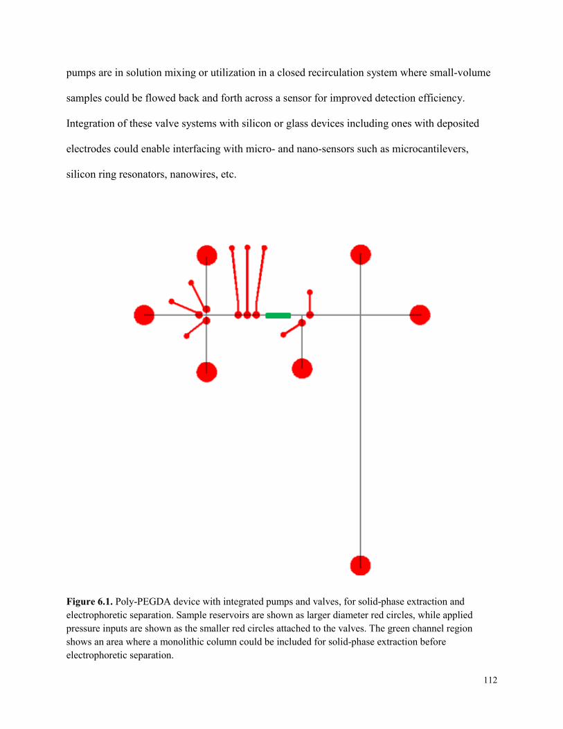
pumps are in solution mixing or utilization in a closed recirculation system where small-volume
samples could be flowed back and forth across a sensor for improved detection efficiency.
Integration of these valve systems with silicon or glass devices including ones with deposited
electrodes could enable interfacing with micro- and nano-sensors such as microcantilevers,
silicon ring resonators, nanowires, etc.
Figure 6.1. Poly-PEGDA device with integrated pumps and valves, for solid-phase extraction and electrophoretic separation. Sample reservoirs are shown as larger diameter red circles, while applied pressure inputs are shown as the smaller red circles attached to the valves. The green channel region shows an area where a monolithic column could be included for solid-phase extraction before electrophoretic separation.
112
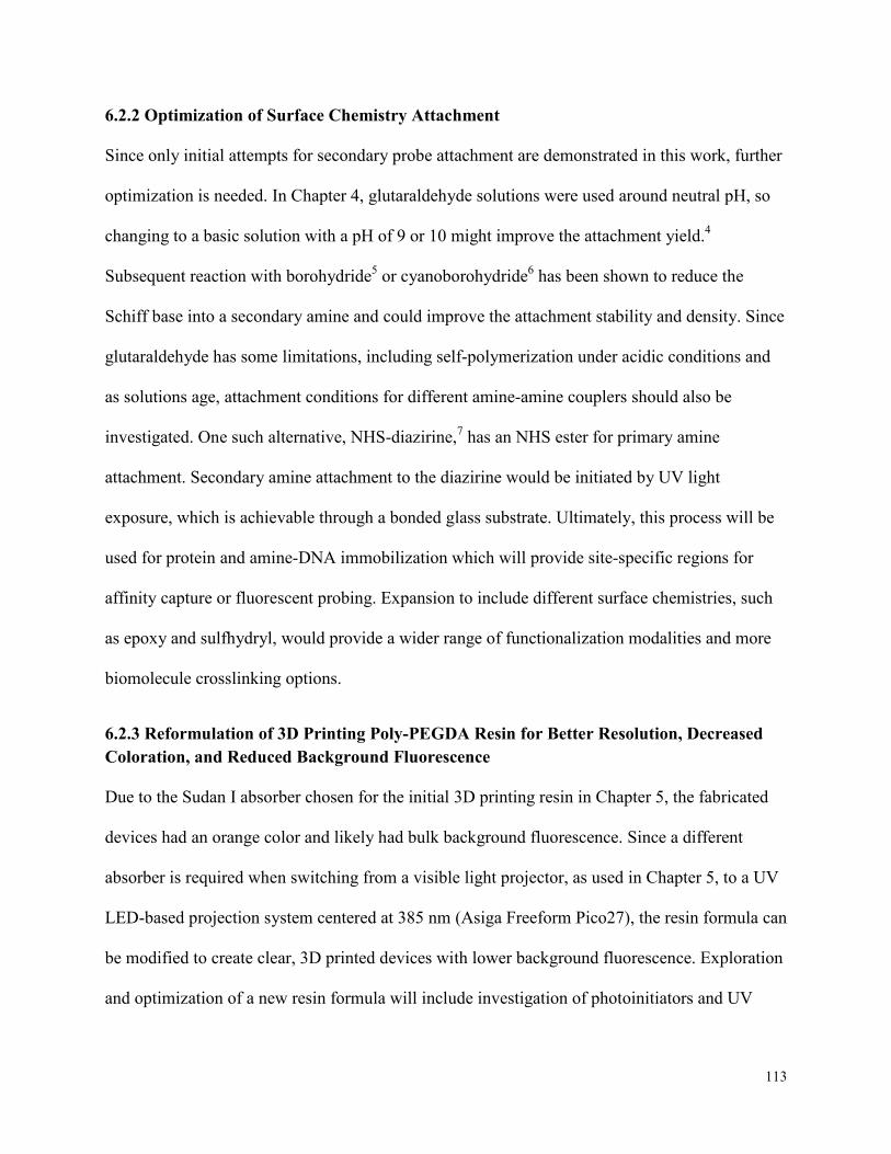
6.2.2 Optimization of Surface Chemistry Attachment
Since only initial attempts for secondary probe attachment are demonstrated in this work, further
optimization is needed. In Chapter 4, glutaraldehyde solutions were used around neutral pH, so
changing to a basic solution with a pH of 9 or 10 might improve the attachment yield.4
Subsequent reaction with borohydride5 or cyanoborohydride6 has been shown to reduce the
Schiff base into a secondary amine and could improve the attachment stability and density. Since
glutaraldehyde has some limitations, including self-polymerization under acidic conditions and
as solutions age, attachment conditions for different amine-amine couplers should also be
investigated. One such alternative, NHS-diazirine,7 has an NHS ester for primary amine
attachment. Secondary amine attachment to the diazirine would be initiated by UV light
exposure, which is achievable through a bonded glass substrate. Ultimately, this process will be
used for protein and amine-DNA immobilization which will provide site-specific regions for
affinity capture or fluorescent probing. Expansion to include different surface chemistries, such
as epoxy and sulfhydryl, would provide a wider range of functionalization modalities and more
biomolecule crosslinking options.
6.2.3 Reformulation of 3D Printing Poly-PEGDA Resin for Better Resolution, Decreased Coloration, and Reduced Background Fluorescence
Due to the Sudan I absorber chosen for the initial 3D printing resin in Chapter 5, the fabricated
devices had an orange color and likely had bulk background fluorescence. Since a different
absorber is required when switching from a visible light projector, as used in Chapter 5, to a UV
LED-based projection system centered at 385 nm (Asiga Freeform Pico27), the resin formula can
be modified to create clear, 3D printed devices with lower background fluorescence. Exploration
and optimization of a new resin formula will include investigation of photoinitiators and UV
113
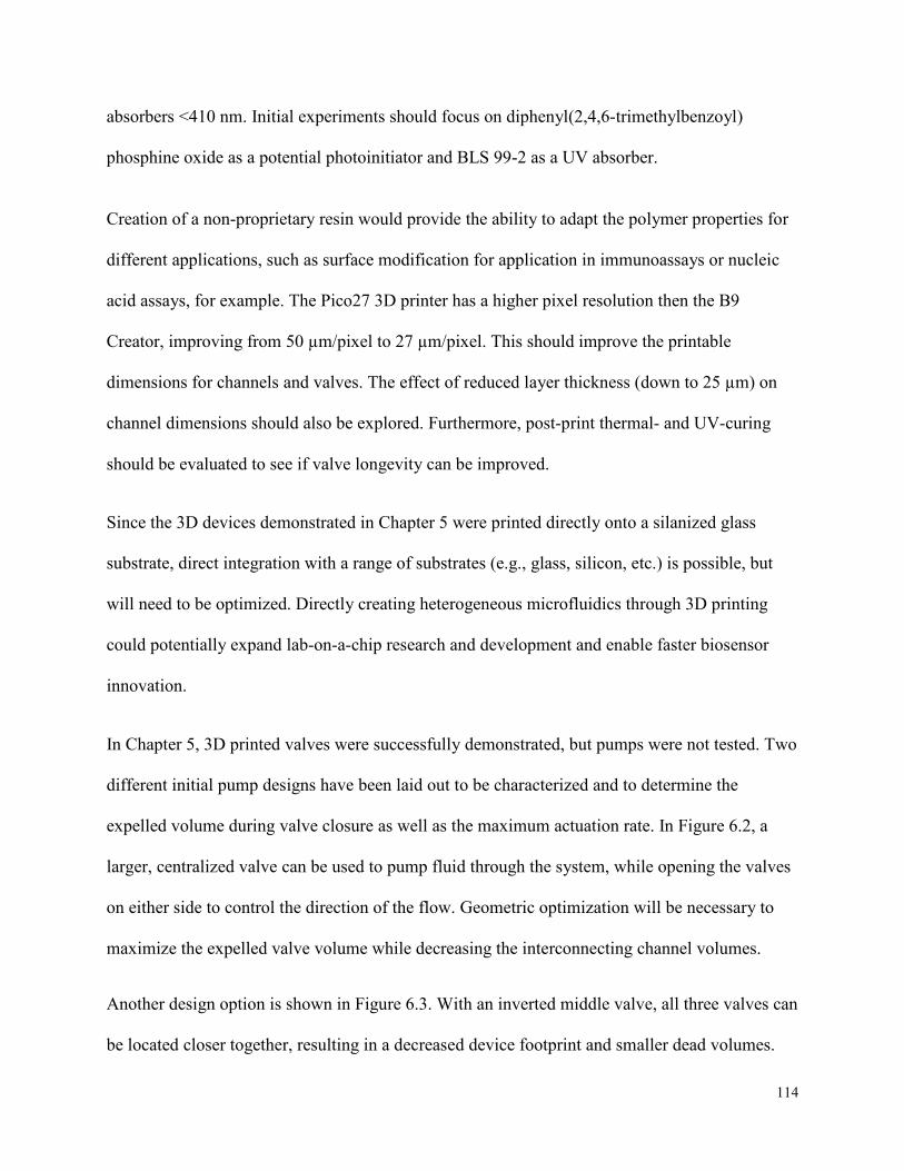
absorbers <410 nm. Initial experiments should focus on diphenyl(2,4,6-trimethylbenzoyl)
phosphine oxide as a potential photoinitiator and BLS 99-2 as a UV absorber.
Creation of a non-proprietary resin would provide the ability to adapt the polymer properties for
different applications, such as surface modification for application in immunoassays or nucleic
acid assays, for example. The Pico27 3D printer has a higher pixel resolution then the B9
Creator, improving from 50 µm/pixel to 27 µm/pixel. This should improve the printable
dimensions for channels and valves. The effect of reduced layer thickness (down to 25 µm) on
channel dimensions should also be explored. Furthermore, post-print thermal- and UV-curing
should be evaluated to see if valve longevity can be improved.
Since the 3D devices demonstrated in Chapter 5 were printed directly onto a silanized glass
substrate, direct integration with a range of substrates (e.g., glass, silicon, etc.) is possible, but
will need to be optimized. Directly creating heterogeneous microfluidics through 3D printing
could potentially expand lab-on-a-chip research and development and enable faster biosensor
innovation.
In Chapter 5, 3D printed valves were successfully demonstrated, but pumps were not tested. Two
different initial pump designs have been laid out to be characterized and to determine the
expelled volume during valve closure as well as the maximum actuation rate. In Figure 6.2, a
larger, centralized valve can be used to pump fluid through the system, while opening the valves
on either side to control the direction of the flow. Geometric optimization will be necessary to
maximize the expelled valve volume while decreasing the interconnecting channel volumes.
Another design option is shown in Figure 6.3. With an inverted middle valve, all three valves can
be located closer together, resulting in a decreased device footprint and smaller dead volumes.
114
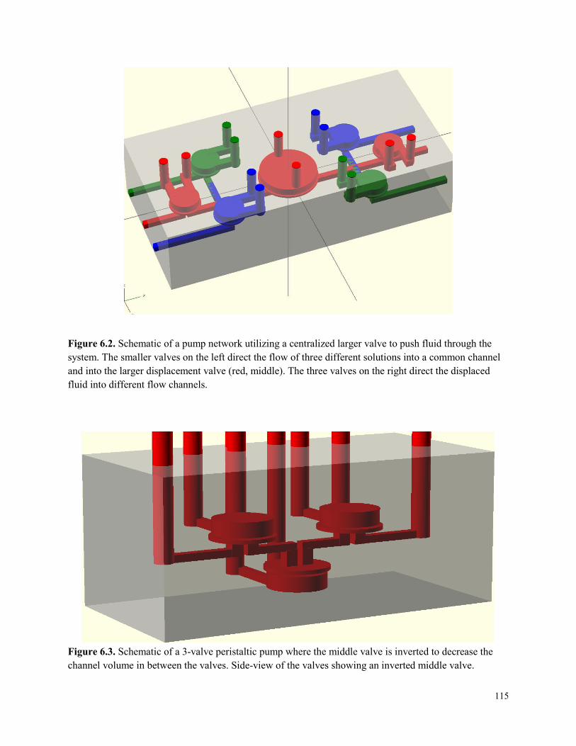
Figure 6.2. Schematic of a pump network utilizing a centralized larger valve to push fluid through the system. The smaller valves on the left direct the flow of three different solutions into a common channel and into the larger displacement valve (red, middle). The three valves on the right direct the displaced fluid into different flow channels.
Figure 6.3. Schematic of a 3-valve peristaltic pump where the middle valve is inverted to decrease the channel volume in between the valves. Side-view of the valves showing an inverted middle valve.
115
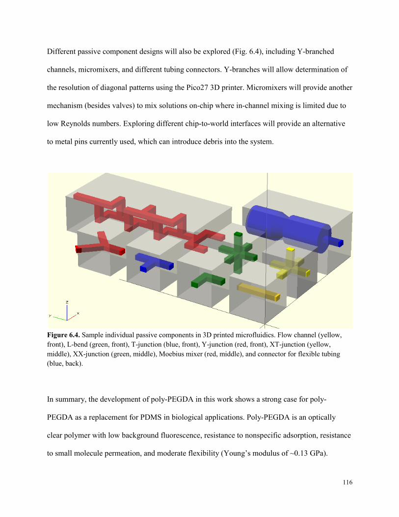
Different passive component designs will also be explored (Fig. 6.4), including Y-branched
channels, micromixers, and different tubing connectors. Y-branches will allow determination of
the resolution of diagonal patterns using the Pico27 3D printer. Micromixers will provide another
mechanism (besides valves) to mix solutions on-chip where in-channel mixing is limited due to
low Reynolds numbers. Exploring different chip-to-world interfaces will provide an alternative
to metal pins currently used, which can introduce debris into the system.
Figure 6.4. Sample individual passive components in 3D printed microfluidics. Flow channel (yellow, front), L-bend (green, front), T-junction (blue, front), Y-junction (red, front), XT-junction (yellow, middle), XX-junction (green, middle), Moebius mixer (red, middle), and connector for flexible tubing (blue, back).
In summary, the development of poly-PEGDA in this work shows a strong case for poly-
PEGDA as a replacement for PDMS in biological applications. Poly-PEGDA is an optically
clear polymer with low background fluorescence, resistance to nonspecific adsorption, resistance
to small molecule permeation, and moderate flexibility (Young’s modulus of ~0.13 GPa).
116
Demonstrated functionality with electrophoretic separations, valve operation, and hybrid
material integration makes poly-PEGDA an excellent candidate for broad use in micro-total
analysis systems, microfluidics, and biosensing. Continued development of poly-PEGDA as a
microfluidic substrate with pumps, other integrated materials, and patterned surface attachment
will provide a more versatile tool for application in this growing field.
6.3 REFERENCES
(1) Yang, W.; Sun, X.; Wang, H.-Y.; Woolley, A. T. Anal. Chem. 2009, 81, 8230-8235. (2) Yang, W.; Sun, X.; Pan, T.; Woolley, A. T. Electrophoresis 2008, 29, 3429-3435. (3) Nge, P. N.; Pagaduan, J. V.; Yu, M.; Woolley, A. T. J. Chromatogr. A 2012, 1261, 129-
135. (4) Hermanson, G. T. Bioconjugate Techniques, 3rd ed.; Academic Press: Boston, MA,
2013, 589-740. (5) Ahmed, S. R.; Kelly, A. B.; Barbari, T. A. J. Membr. Sci. 2006, 280, 553-559. (6) Park, M. K.; Kee, J. S.; Quah, J. Y.; Netto, V.; Song, J.; Fang, Q.; La Fosse, E. M.; Lo,
G.-Q. Sens. Actuators, B 2013, 176, 552-559. (7) Gomes, A. F.; Gozzo, F. C. J. Mass Spectrom. 2010, 45, 892-899.
117