
Optically pumped nanowire lasers - Harvard University
13
Semiconductor Science and Technology TOPICAL REVIEW Optically pumped nanowire lasers: invited review To cite this article: Mariano A Zimmler et al 2010 Semicond. Sci. Technol. 25 024001 View the article online for updates and enhancements. Related content GaAs–AlGaAs core–shell nanowire lasers on silicon: invited review Gregor Koblmüller, Benedikt Mayer, Thomas Stettner et al. - Semiconductor plasmonic nanolasers: current status and perspectives Shangjr Gwo and Chih-Kang Shih - Low threshold room-temperature lasing of CdS nanowires Sebastian Geburt, Andreas Thielmann, Robert Röder et al. - Recent citations Spectral narrowing and pulse shortening of an amplified spontaneous emission from oriented ZnO nanorods S.S. Kurbanov et al - Recent advances in synthesis and application of perovskite quantum dot based composites for photonics, electronics and sensors Yaxin Wang et al - Heterostructure and Q-factor engineering for low-threshold and persistent nanowire lasing Stefan Skalsky et al - This content was downloaded from IP address 128.103.24.178 on 24/05/2020 at 02:10
Transcript of Optically pumped nanowire lasers - Harvard University

Semiconductor Science and Technology
TOPICAL REVIEW
Optically pumped nanowire lasers: invited reviewTo cite this article: Mariano A Zimmler et al 2010 Semicond. Sci. Technol. 25 024001
View the article online for updates and enhancements.
Related contentGaAs–AlGaAs core–shell nanowire laserson silicon: invited reviewGregor Koblmüller, Benedikt Mayer,Thomas Stettner et al.
-
Semiconductor plasmonic nanolasers:current status and perspectivesShangjr Gwo and Chih-Kang Shih
-
Low threshold room-temperature lasing ofCdS nanowiresSebastian Geburt, Andreas Thielmann,Robert Röder et al.
-
Recent citationsSpectral narrowing and pulse shorteningof an amplified spontaneous emission fromoriented ZnO nanorodsS.S. Kurbanov et al
-
Recent advances in synthesis andapplication of perovskite quantum dotbased composites for photonics,electronics and sensorsYaxin Wang et al
-
Heterostructure and Q-factor engineeringfor low-threshold and persistent nanowirelasingStefan Skalsky et al
-
This content was downloaded from IP address 128.103.24.178 on 24/05/2020 at 02:10
IOP PUBLISHING SEMICONDUCTOR SCIENCE AND TECHNOLOGY
Semicond. Sci. Technol. 25 (2010) 024001 (12pp) doi:10.1088/0268-1242/25/2/024001
TOPICAL REVIEW
Optically pumped nanowire lasers:invited reviewMariano A Zimmler1, Federico Capasso1, Sven Muller2
and Carsten Ronning3
1 School of Engineering and Applied Sciences, Harvard University, Cambridge, MA 02138, USA2 II Institute of Physics, University of Gottingen, 37077 Gottingen, Germany3 Institute for Solid State Physics, University of Jena, 00743 Jena, Germany
E-mail: [email protected]
Received 27 April 2009Published 22 January 2010Online at stacks.iop.org/SST/25/024001
AbstractThis paper reviews several topics related to optically pumped ZnO nanowire lasers. Asystematic study of the various properties of a device as it evolves from the regime ofamplified spontaneous emission to laser oscillation above threshold is presented. The keydependence of the laser threshold on nanowire diameter is demonstrated and explained bymeans of a thorough study of guided modes in semiconducting nanowires for ananowire-on-substrate geometry. A ‘head on’ detection geometry is used to measure thefar-field profile of a nanowire laser and thus identify the modes responsible for lasing. Finally,the temperature behavior of a nanowire laser is reported, and possible mechanisms that may beresponsible for gain are suggested.
(Some figures in this article are in colour only in the electronic version)
1. Introduction
The possibility of laser action in semiconductor nanowires isnothing short of intriguing. Such devices could potentiallygenerate highly localized intense monochromatic light ina geometry ideally suited for the efficient coupling intonanophotonic elements such as quantum dots, metallicnanoparticles, plasmonic waveguides and even biologicalspecimens. Thus, nanowire lasers could become a criticalcomponent in the study and development of novel nanoscalephotonic elements. The research community has consequentlyextended significant efforts toward their realization, but moststudies have succeeded only in providing evidence of amplifiedspontaneous emission (ASE) [1–8]. While more recentwork on gallium antimonide (GaSb) nanowires [9] showssome evidence of lasing, the conclusive demonstration oflaser oscillation has remained elusive. In particular, mostworks have failed to observe a laser threshold marking thetransition between a superlinear region, characteristic of ASE,and a linear region, characteristic of laser oscillation, withincreasing pump power or drive current [10]. Furthermore,the study of individual nanowires has usually been conducted
in an epifluorescence setup. In such a configuration, a singlemicroscope objective is used for excitation and collection, sothat only light scattered at 90◦ from the nanowire axis can becollected, preventing a full characterization of the angular andpolarization dependence of the laser emission.
Recently, we reported direct evidence of laser actionin optically pumped nanowires [11]. In that work,we successfully observed the transition from ASE tolaser oscillation in ZnO nanowires at room temperature.Furthermore, we introduced a ‘head on’ detectionconfiguration that permitted the first accurate measurementof the power emitted by a single nanowire.
In this paper, we review our previous work and present, inaddition, a complete study of the mode structure of nanowiresin a nanowire-on-substrate geometry. We also extend our headon detection results to include the first measurement of the far-field profile of a single nanowire. Finally, we also presentresults on the temperature behavior of our devices.
Laser oscillation occurs when the cavity round-trip gainequals the round-trip losses [10], which in nanowires aretypically dominated by the mirror losses (that is, transmissionat the end facets). This is the result of diffraction: when the
0268-1242/10/024001+12$30.00 1 © 2010 IOP Publishing Ltd Printed in the UK
Semicond. Sci. Technol. 25 (2010) 024001 Topical Review
diameter of the nanowire is comparable to or smaller than thewavelength of light in the semiconductor, the optical field canextend considerably outside the nanowire. This contributesto the mirror losses because only the fraction of the field thatis confined inside the nanowire experiences a refractive indexcontrast at the end facets, therefore limiting the amount ofreflection and feedback. Thus, it would appear that we arefaced with a fundamental trade-off: while narrow-diameternanowires satisfy our need for compactness, they presentlarge losses which might prevent lasing. We will explorethis relationship below.
This paper is structured as follows. We begin with apresentation of unambiguous evidence of optically pumpedlaser action in ZnO nanowires, which is supported by theobservation of a clear transition between ASE and laseroscillation. By systematically studying nanowires of differentdimensions, we then demonstrate the existence of a criticaldiameter below which no lasing occurs. In order to understandsuch behavior quantitatively, we next solve for the dispersionproperties of a ZnO nanowire on a silica substrate and computethe facet reflectivity for a few of the lowest-order guidedmodes. Armed with these tools, we estimate diameter andlength dependence of the threshold gain for our nanowires andcompare this to our experimental findings. Next, we introducean alternative ‘head on’ detection geometry, with which wemeasure the far-field profile of a single nanowire laser andthus identify the oscillating modes. Finally, we present acursory examination of the temperature dependence of lasingin these devices and suggest possible gain mechanisms whichmay be at work.
2. Synthesis
The ZnO nanowires used in this work were synthesized with aVLS technique [12]. The distinguishing feature of the processpresented here is the use of pure ZnO powder, rather thana combination of ZnO and graphite, as the source material.The powder was placed in an alumina boat at the center of ahorizontal tube furnace and heated up to 1350 ◦C, at a rate of190 ◦C h−1, and kept at this temperature for the duration ofthe growth (30 min). The resulting ZnO vapor was transportedwith argon gas (50 sccm flow rate at a system pressure between100 and 200 mbar) to a position in the furnace where thetemperature ranged between 960 and 1150 ◦C, and where itcondensed to form nanowires on an Au-covered (with a 4 nmthick film) silicon substrate. Only during the growth at1350 ◦C was the argon flow direction set to transport the ZnOvapor from the source to the substrate. During the heating-upand cooling-down phases the gas flow direction was reversed.A growth duration of 30 min results in a dense sample ofrandomly arranged ZnO nanowires, as shown in the SEMimage in the inset of figure 1. The nanowires exhibit a broaddiameter distribution between 100 and 400 nm and lengths upto 100 μm.
3. Structural characterization
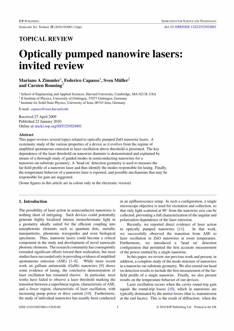
Figure 1 shows a representative �–2� x-ray diffraction (XRD)spectrum (taken with a D8 Discover Bruker AXS spectrometer
Figure 1. Representative x-diffraction spectrum of an as-grownZnO nanowire ensemble sample. Inset (left): SEM micrograph ofthe as-grown ensemble of ZnO nanowires on the growth substrate.The scale bar is 10 μm. Inset (right): SEM micrograph of a singleZnO nanowire. The scale bar is 500 nm.
(a) (b)
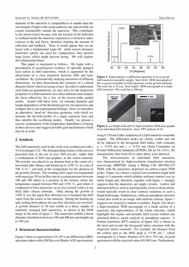
Figure 2. (a) Bright-field and (b) high-resolution TEM micrographsof an individual ZnO nanowire. Inset: FFT analysis of (b).
using 0.154 nm CuKα radiation) of a ZnO nanowire ensemblesample. The diffraction peaks are clearly visible and canall be indexed to the hexagonal ZnO lattice with constantsa = 0.325 nm and c = 0.521 nm (Joint Committee onPowder Diffraction Standards (JCPDS), file no 36–1451). Nocharacteristic lines from Zn or other alloys were detected.
The microstructure of individual ZnO nanowireswas characterized by high-resolution transmission electronmicroscopy (HRTEM) (using a Philips CM 200-FEG-UTTEM, with the nanowires dispersed on carbon-coated TEMgrids). Figure 2(a) shows a typical low-resolution bright fieldimage of a nanowire which exhibits uniform contrast over itsentire length and, therefore, together with figure 1, stronglysuggests that the nanowires are single crystals. Lattice andstructural defects, such as stacking faults, twins or dislocations,would typically result in clear contrast variations in such abright field image. Furthermore, while an amorphous structurewould also result in an image with uniform contrast, figure 1suggests our material is indeed crystalline. Figure 2(b) showsa high-resolution TEM micrograph of a small section of ananowire, but representative of the whole structure, whichhighlights the regular and periodic ZnO crystal without anystructural defects, metal catalysts or amorphous regions. AFourier transform (FFT) analysis of figure 2(b) is shown inthe inset and reveals the hexagonal lattice structure with therespective lattice constants. For example, the distance fromthe central spot to the 0002 peak is ≈3.99 nm−1, whichcorresponds to a lattice distance of 0.25(± 5%) nm, in goodagreement with the expected value of 0.2603 nm. Furthermore,
2

Semicond. Sci. Technol. 25 (2010) 024001 Topical Review
we can clearly see from the TEM analysis that the ZnOnanowires grow, in general, in the c-axis direction, whichis in agreement with the literature [13].
4. Amplified spontaneous emission and laseroscillation
After growth, the nanowires were dispersed onto a Si/SiO2
substrate (with a 500 nm thick thermal oxide) for opticalcharacterization. Individual nanowires were pumped with thefrequency-tripled output (355 nm) of a Nd:YAG laser (500 Hz,6 ns pulse length), focused to a diameter of ∼100 μm, using areflective microscope objective. The excitation intensity wasattenuated by changing the Q-switch delay of our pump lasertogether with the use of neutral density filters. Their emissionwas collected with the same objective. All measurements wereperformed at room temperature, unless otherwise noted. Whilelimited in its utility for the study of the angular and polarizationdependence of the facet emission, this configuration enablesus to study a large number of nanowires of varying lengthsand diameters, which is necessary to elucidate the thresholddependence on nanowire dimensions.
Figures 3(a) and (b) show the luminescence spectra andthe corresponding CCD images, respectively, for a ZnOnanowire as a function of pump intensity Iex. For Iex �200 kW cm−2, the spectra are broad and featureless, centeredaround ∼382 nm and with a full-width at half-maximum(FWHM) of 19.3 nm. In this regime, light is emittedessentially isotropically along the nanowire—as seen in thesecond panel from the bottom of figure 3(b)—and the outputpower (shown in figures 3(c) and (d)) depends linearly on theexcitation intensity, consistent with spontaneous emission. For200 kW cm−2 � Iex � 300 kW cm−2, the spectra consist of abroad emission with the addition of sharp (FWHM < 0.4 nm)emission lines. In this regime, population inversion startsbuilding up, leading to ASE along the nanowire at wavelengthscorresponding to the longitudinal modes (see section 5)and thus to enhanced emission from the nanowire ends.Furthermore, the output power exhibits a superlinear increasewith pump intensity, which is the expected behavior asthe laser threshold is approached [10, 14]. For Iex �300 kW cm−2, the spectra are dominated by sharp emissionlines: their intensity is orders of magnitude greater than thespontaneous emission background. The output power dependslinearly on excitation intensity and is concentrated in a narrowemission range (385 nm < λ < 390 nm). Figure 3(c) alsoshows a fit (solid line) with a multimode laser model [14],which gives a threshold of �270 kW cm−2. The theoryin [14] gives the output power of the laser as a functionof the normalized pump rate and a parameter x0, which isproportional to the mode density (see equation (23)). Anexcellent fit of this equation to the data is obtained withx0 = 0.016. Figure 3(d) shows the same data and fit asfigure 3(c) on a log–log scale. Note that the threshold insemiconductor lasers is ‘softer’ than in other lasers due tothe small cavity volume and the relatively high levels ofspontaneous emission [10, 14]. In summary, the data offigure 3 show the expected behavior of the output power of thenanowire device as it passes through the threshold for laseroscillation.
(a) (b)
(c) (d )
Figure 3. Laser oscillation in ZnO nanowires. (a) Output spectraversus pump intensity of a 12.2 μm long 250 nm diameter ZnOnanowire. (b) SEM image and CCD images, under different pumpintensities, for the same nanowire as in (a). The labels indicate thepump intensity in units of MW cm−2. The color scale indicates thenumber of counts. (c) Pump intensity dependence of the total outputpower (circles) for the same nanowire. The solid line is a fit to thedata using the model in [14]. The optical power was collected fromthe scattered light at one of the nanowire ends. (d) The same dataand fit on a log–log scale. The open circles correspond to the spectrashown in (a).
5. Fabry–Perot waveguide modes
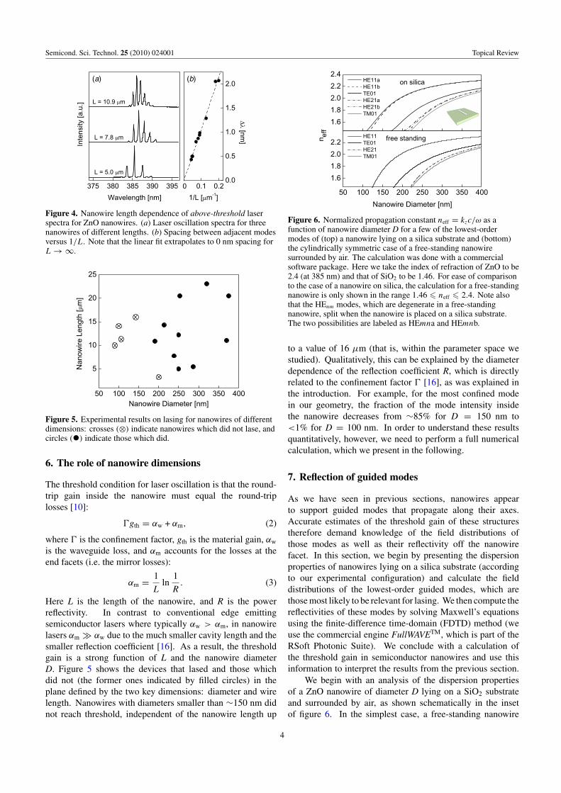
The sharp features observed in figure 3(a) correspond tolongitudinal Fabry–Perot waveguide modes. The modespacing in a Fabry–Perot cavity is given by [10]
�λ = 1
L
[λ2
2
(n − λ
dn
dλ
)−1]
, (1)
where L is the cavity length, and n is the index of refraction atwavelength λ. Thus, for a fixed λ, the mode spacing �λ shouldscale in proportion to the inverse length 1/L. This behavior isillustrated in figure 4(b), which shows above-threshold spectrafor nanowires of different lengths and a plot of �λ for ninenanowires. The slope of the fit is 10 765(±1.7%) nm2. Withλ = 385 nm and n = 2.4, this gives dn/dλ ≈ −0.012 nm−1.This value is in reasonable agreement with published data forZnO [15], which gives dn/dλ ≈ −0.015 nm−1.
3
Semicond. Sci. Technol. 25 (2010) 024001 Topical Review
(a) (b)
Figure 4. Nanowire length dependence of above-threshold laserspectra for ZnO nanowires. (a) Laser oscillation spectra for threenanowires of different lengths. (b) Spacing between adjacent modesversus 1/L. Note that the linear fit extrapolates to 0 nm spacing forL → ∞.
Figure 5. Experimental results on lasing for nanowires of differentdimensions: crosses (⊗) indicate nanowires which did not lase, andcircles (•) indicate those which did.
6. The role of nanowire dimensions
The threshold condition for laser oscillation is that the round-trip gain inside the nanowire must equal the round-triplosses [10]:
�gth = αw + αm, (2)
where � is the confinement factor, gth is the material gain, αw
is the waveguide loss, and αm accounts for the losses at theend facets (i.e. the mirror losses):
αm = 1
Lln
1
R. (3)
Here L is the length of the nanowire, and R is the powerreflectivity. In contrast to conventional edge emittingsemiconductor lasers where typically αw > αm, in nanowirelasers αm αw due to the much smaller cavity length and thesmaller reflection coefficient [16]. As a result, the thresholdgain is a strong function of L and the nanowire diameterD. Figure 5 shows the devices that lased and those whichdid not (the former ones indicated by filled circles) in theplane defined by the two key dimensions: diameter and wirelength. Nanowires with diameters smaller than ∼150 nm didnot reach threshold, independent of the nanowire length up
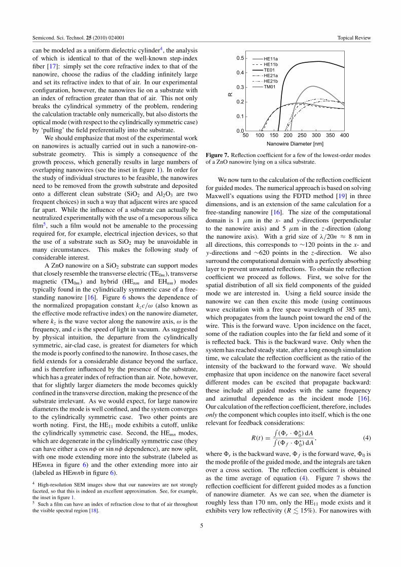
Figure 6. Normalized propagation constant neff = kzc/ω as afunction of nanowire diameter D for a few of the lowest-ordermodes of (top) a nanowire lying on a silica substrate and (bottom)the cylindrically symmetric case of a free-standing nanowiresurrounded by air. The calculation was done with a commercialsoftware package. Here we take the index of refraction of ZnO to be2.4 (at 385 nm) and that of SiO2 to be 1.46. For ease of comparisonto the case of a nanowire on silica, the calculation for a free-standingnanowire is only shown in the range 1.46 � neff � 2.4. Note alsothat the HEnm modes, which are degenerate in a free-standingnanowire, split when the nanowire is placed on a silica substrate.The two possibilities are labeled as HEmna and HEmnb.
to a value of 16 μm (that is, within the parameter space westudied). Qualitatively, this can be explained by the diameterdependence of the reflection coefficient R, which is directlyrelated to the confinement factor � [16], as was explained inthe introduction. For example, for the most confined modein our geometry, the fraction of the mode intensity insidethe nanowire decreases from ∼85% for D = 150 nm to<1% for D = 100 nm. In order to understand these resultsquantitatively, however, we need to perform a full numericalcalculation, which we present in the following.
7. Reflection of guided modes
As we have seen in previous sections, nanowires appearto support guided modes that propagate along their axes.Accurate estimates of the threshold gain of these structurestherefore demand knowledge of the field distributions ofthose modes as well as their reflectivity off the nanowirefacet. In this section, we begin by presenting the dispersionproperties of nanowires lying on a silica substrate (accordingto our experimental configuration) and calculate the fielddistributions of the lowest-order guided modes, which arethose most likely to be relevant for lasing. We then compute thereflectivities of these modes by solving Maxwell’s equationsusing the finite-difference time-domain (FDTD) method (weuse the commercial engine FullWAVETM, which is part of theRSoft Photonic Suite). We conclude with a calculation ofthe threshold gain in semiconductor nanowires and use thisinformation to interpret the results from the previous section.
We begin with an analysis of the dispersion propertiesof a ZnO nanowire of diameter D lying on a SiO2 substrateand surrounded by air, as shown schematically in the insetof figure 6. In the simplest case, a free-standing nanowire
4
Semicond. Sci. Technol. 25 (2010) 024001 Topical Review
can be modeled as a uniform dielectric cylinder4, the analysisof which is identical to that of the well-known step-indexfiber [17]: simply set the core refractive index to that of thenanowire, choose the radius of the cladding infinitely largeand set its refractive index to that of air. In our experimentalconfiguration, however, the nanowires lie on a substrate withan index of refraction greater than that of air. This not onlybreaks the cylindrical symmetry of the problem, renderingthe calculation tractable only numerically, but also distorts theoptical mode (with respect to the cylindrically symmetric case)by ‘pulling’ the field preferentially into the substrate.
We should emphasize that most of the experimental workon nanowires is actually carried out in such a nanowire-on-substrate geometry. This is simply a consequence of thegrowth process, which generally results in large numbers ofoverlapping nanowires (see the inset in figure 1). In order forthe study of individual structures to be feasible, the nanowiresneed to be removed from the growth substrate and depositedonto a different clean substrate (SiO2 and Al2O3 are twofrequent choices) in such a way that adjacent wires are spacedfar apart. While the influence of a substrate can actually beneutralized experimentally with the use of a mesoporous silicafilm5, such a film would not be amenable to the processingrequired for, for example, electrical injection devices, so thatthe use of a substrate such as SiO2 may be unavoidable inmany circumstances. This makes the following study ofconsiderable interest.
A ZnO nanowire on a SiO2 substrate can support modesthat closely resemble the transverse electric (TE0m), transversemagnetic (TM0m) and hybrid (HEnm and EHnm) modestypically found in the cylindrically symmetric case of a free-standing nanowire [16]. Figure 6 shows the dependence ofthe normalized propagation constant kzc/ω (also known asthe effective mode refractive index) on the nanowire diameter,where kz is the wave vector along the nanowire axis, ω is thefrequency, and c is the speed of light in vacuum. As suggestedby physical intuition, the departure from the cylindricallysymmetric, air-clad case, is greatest for diameters for whichthe mode is poorly confined to the nanowire. In those cases, thefield extends for a considerable distance beyond the surface,and is therefore influenced by the presence of the substrate,which has a greater index of refraction than air. Note, however,that for slightly larger diameters the mode becomes quicklyconfined in the transverse direction, making the presence of thesubstrate irrelevant. As we would expect, for large nanowirediameters the mode is well confined, and the system convergesto the cylindrically symmetric case. Two other points areworth noting. First, the HE11 mode exhibits a cutoff, unlikethe cylindrically symmetric case. Second, the HEmn modes,which are degenerate in the cylindrically symmetric case (theycan have either a cos nφ or sin nφ dependence), are now split,with one mode extending more into the substrate (labeled asHEmna in figure 6) and the other extending more into air(labeled as HEmnb in figure 6).
4 High-resolution SEM images show that our nanowires are not stronglyfaceted, so that this is indeed an excellent approximation. See, for example,the inset in figure 1.5 Such a film can have an index of refraction close to that of air throughoutthe visible spectral region [18].
Figure 7. Reflection coefficient for a few of the lowest-order modesof a ZnO nanowire lying on a silica substrate.
We now turn to the calculation of the reflection coefficientfor guided modes. The numerical approach is based on solvingMaxwell’s equations using the FDTD method [19] in threedimensions, and is an extension of the same calculation for afree-standing nanowire [16]. The size of the computationaldomain is 1 μm in the x- and y-directions (perpendicularto the nanowire axis) and 5 μm in the z-direction (alongthe nanowire axis). With a grid size of λ/20n ≈ 8 nm inall directions, this corresponds to ∼120 points in the x- andy-directions and ∼620 points in the z-direction. We alsosurround the computational domain with a perfectly absorbinglayer to prevent unwanted reflections. To obtain the reflectioncoefficient we proceed as follows. First, we solve for thespatial distribution of all six field components of the guidedmode we are interested in. Using a field source inside thenanowire we can then excite this mode (using continuouswave excitation with a free space wavelength of 385 nm),which propagates from the launch point toward the end of thewire. This is the forward wave. Upon incidence on the facet,some of the radiation couples into the far field and some of itis reflected back. This is the backward wave. Only when thesystem has reached steady state, after a long enough simulationtime, we calculate the reflection coefficient as the ratio of theintensity of the backward to the forward wave. We shouldemphasize that upon incidence on the nanowire facet severaldifferent modes can be excited that propagate backward:these include all guided modes with the same frequencyand azimuthal dependence as the incident mode [16].Our calculation of the reflection coefficient, therefore, includesonly the component which couples into itself, which is the onerelevant for feedback considerations:
R(t) =∫(r · ∗
0) dA∫(f · ∗
0) dA, (4)
where r is the backward wave, f is the forward wave, 0 isthe mode profile of the guided mode, and the integrals are takenover a cross section. The reflection coefficient is obtainedas the time average of equation (4). Figure 7 shows thereflection coefficient for different guided modes as a functionof nanowire diameter. As we can see, when the diameter isroughly less than 170 nm, only the HE11 mode exists and itexhibits very low reflectivity (R � 15%). For nanowires with
5

Semicond. Sci. Technol. 25 (2010) 024001 Topical Review
Figure 8. Threshold gain, as given by equation (2), for a ZnOnanowire lying on a silica substrate, with the assumption thatαm αw, as a function of nanowire diameter and for severalnanowire lengths.
diameters larger than 170 nm, on the other hand, several othermodes are possible. Of these, the TE01 mode exhibits thelargest reflectivity, R ≈ 47%, almost as soon as the mode isallowed, which is more than twice the reflectivity of the HE11
mode, and roughly 50% larger than the maximum value forthe TM01 mode. In figure 8, we have used the results of thereflectivity calculation for the various modes, in conjunctionwith equations (2) and (3), to calculate the threshold gainfor nanowires of various dimensions. Figure 8 reinforces theconclusions reached from the reflectivity data. For nanowireswith D � 170 nm, the TE01 mode clearly exhibits the lowestthresholds, which can be up to one order of magnitude lowerthan the threshold for nanowires with D < 150 nm (for thesame nanowire length), for which only the HE11 mode exists.For nanowires with D � 200 nm, the TM01 mode is alsopossible and it exhibits the next higher thresholds, which areapproximately 50% larger than those corresponding to theTE01 mode. These results suggest that the TE01 and TM01
modes are the most likely to lase for nanowires with diameterslarger than 170 nm, whereas when D < 170 nm, if lasingis at all possible given the sharp increase in the threshold,nanowires would lase in the HE11 mode.
8. Mode confinement
As we have explained above, the threshold condition for laseroscillation is given by �gth = αw + αm. The expression, �gth,is commonly referred to as the modal gain, i.e. the percentagepower increase per unit length along the propagation directiongained by the waveguide mode from the active region. Theconfinement factor � is usually taken to mean the fraction ofthe optical mode intensity contained within the active region[20]. This, however, is not entirely accurate for semiconductornanowires6. The modal gain is, in fact, defined as the growthrate of power in the waveguide by means of the expression
dP(z)
dz= �gP (z). (5)
6 We thank Professor Cun-Zheng Ning for bringing this to our attention. See[21] for a full discussion.
Figure 9. Confinement factor for a few of the lowest-order modesof a ZnO nanowire lying on a silica substrate.
Here P(z) is the power as a function of distance along thewaveguide, and g stands for the material gain (we assumeisotropic gain for simplicity). The confinement factor is thengiven by [21]
� = c√
ε
2πP0
∫nw
|E|2 dA, (6)
where ε is the dielectric constant of the nanowire, and E is thecomplex electric field. The integral is over a nanowire crosssection, and P0 is given by
P0 =∫
(S + S∗)z dA, S = c
4πE × H∗, (7)
with S being the Poynting vector (i.e. P0 is an integral of thetime averaged energy flux over an infinite plane perpendicularto the direction of propagation). Thus, the confinement factorcan be calculated directly from the field distributions. In thelimiting case of weak waveguiding [21], the confinement factorbecomes the ratio of the power inside the nanowire to the totalpower, as is usually assumed in the literature. However, forstrong waveguiding, the confinement factor can exceed unity.As discussed in [21], this phenomenon can be understoodphysically by noting that, in a planar waveguide, a guidedwave can be represented as a plane wave that propagatesat some angle with respect to the z-direction, and thereforeexperiences multiple reflections at the waveguide boundaries.The total distanced traveled by this wave is larger than fora plane wave propagating along the z-direction, so that thegain per unit distance along the z-direction can be larger if thewave is well confined to the active region. Figure 9 showsthe confinement factors for a ZnO nanowire lying on a silicasubstrate, calculated according to equation (6).
9. ‘Head on’ measurements
As we have seen in the last two sections, a ZnO semiconductornanowire can theoretically support several optical modesexhibiting different dispersion, polarization, field distributionsand losses. Naturally, a complete study of a nanowire laserdemands that we determine which of these modes actuallyoccurs in practice and under what conditions. This can bedone with a full characterization of the far-field emission that
6
Semicond. Sci. Technol. 25 (2010) 024001 Topical Review
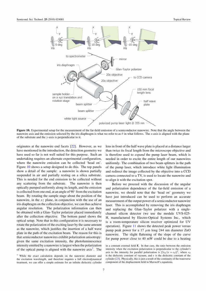
Figure 10. Experimental setup for the measurement of the far-field emission of a semiconductor nanowire. Note that the angle between thenanowire axis and the emission selected by the iris diaphragm is what we refer to as θ in what follows. The x-axis is aligned with the planeof the substrate and the y-axis is perpendicular to it.
originates at the nanowire end facets [22]. However, as wehave mentioned in the introduction, the detection geometry wehave used so far is not well suited for this purpose. Such anundertaking requires an alternate experimental configuration,where the nanowire emission can be collected ‘head on’.Figure 10 shows a setup designed to do this. The top panelsshow a detail of the sample: a nanowire is shown partiallysuspended in air and partially resting on a silica substrate.This is needed for the end emission to be collected withoutany scattering from the substrate. The nanowire is thenoptically pumped uniformly along its length, and the emissionis collected from one end, at an angle of 90◦ from the excitationbeam. By rotating the sample stage about the position of thenanowire, in the xz plane, in conjunction with the use of aniris diaphragm on the collection objective, we can thus achieveangular resolution. The polarization information can thenbe obtained with a Glan–Taylor polarizer placed immediatelyafter the collection objective. The bottom panel shows theoptical setup. Note that in this configuration it is necessary torotate the polarization of the exciting laser by the same amountas the nanowire, which justifies the insertion of a half waveplate in the path of the excitation beam. The reason for this isthat semiconductor nanowires exhibit polarization anisotropy:given the same excitation intensity, the photoluminescenceintensity emitted by a nanowire is largest when the polarizationof the optical pump is aligned with the nanowire axis7. The
7 While the exact calculation depends on the nanowire diameter andthe excitation wavelength, and therefore requires a full electrodynamicaltreatment, we can offer a simple estimate for an infinite dielectric cylinder
lens in front of the half wave plate is placed at a distance largerthan twice its focal length from the microscope objective andis therefore used to expand the pump laser beam, which isneeded in order to excite the entire length of our nanowiresuniformly. The combination of two beam splitters in the pathof the pump laser, which introduce white light illuminationand redirect the image collected by the objective into a CCDcamera connected to a TV, is used to locate the nanowire andto align it with the excitation spot.
Before we proceed with the discussion of the angularand polarization dependence of the far-field emission of ananowire, we should note that the ‘head on’ geometry wehave just introduced can be used to perform an accuratemeasurement of the output power of a semiconductor nanowirelaser. This is accomplished by removing the iris diaphragmand replacing the Glan–Taylor polarizer with a single-channel silicon detector (we use the module UVS-025-H, manufactured by Electro-Optical Systems Inc., whichis a room-temperature silicon receiver optimized for UVoperation). Figure 11 shows the detected peak power versuspump peak power for a 17 μm long 244 nm diameter ZnOnanowire. The slight flattening of the slope of the curvefor pump power close to 40 mW could be due to a heating
in a constant external field E. In that case, the ratio between the emissionintensity when the excitation polarization is perpendicular to the cylinder’saxis to the intensity for parallel polarization is [2ε0/(ε + ε0)]2, where ε0is the dielectric constant of vacuum, and ε is the dielectric constant of thecylinder [23]. Physically, this is just a result of the continuity of the transversecomponent of the displacement field in Maxwell’s equations.
7
Semicond. Sci. Technol. 25 (2010) 024001 Topical Review
Figure 11. Peak optical power, uncorrected for the collectionefficiency (10%), measured ‘head on’ at the nanowire end.
effect. The inset shows an SEM image of the sample (comparewith the top panel in figure 10). While we presently lack arobust method to prepare these samples, we have found that byfirst depositing nanowires onto a Si/SiO2 substrate and thencleaving it into several smaller pieces typically results in a fewpartially suspended nanowires.
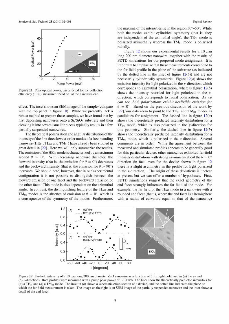
The theoretical polarization and angular distribution of theintensity of the first three lowest-order modes of a free-standingnanowire (HE11, TE01 and TM01) have already been studied ingreat detail in [22]. Here we will only summarize the results.The emission of the HE11 mode is characterized by a maximumaround θ = 0◦. With increasing nanowire diameter, theforward intensity (that is, the emission for θ = 0◦) decreasesand the backward intensity (that is, the emission for θ > 90◦)increases. We should note, however, that in our experimentalconfiguration it is not possible to distinguish between theforward emission of one facet and the backward emission ofthe other facet. This mode is also dependent on the azimuthalangle. In contrast, the distinguishing feature of the TE01 andTM01 modes is the absence of emission at θ = 0◦, which isa consequence of the symmetry of the modes. Furthermore,
(a)
(b)
Figure 12. Far-field intensity of a 10 μm long 200 nm diameter ZnO nanowire as a function of θ for light polarized in (a) the y- and(b) x-directions. Both profiles were measured with a pump peak power of ∼10 mW. The lines show the theoretically predicted intensities for(a) a TE01 and (b) a TM01 mode. The inset in (b) shows a schematic cross section of a device, and the dotted line indicates the plane onwhich the far-field measurement is taken. The image on the right is an SEM image of the partially suspended nanowire and the inset shows adetail of the end facet.
the maxima of the intensities lie in the region 30◦–50◦. Whileboth the modes exhibit cylindrical symmetry (that is, theyare independent of the azimuthal angle), the TE01 mode ispolarized azimuthally whereas the TM01 mode is polarizedradially.
Figure 12 shows our experimental results for a 10 μmlong 200 nm diameter nanowire, together with the results ofFDTD simulations for our proposed mode assignment. It isimportant to emphasize that these measurements correspond tothe far-field profile in the plane of the substrate (as indicatedby the dotted line in the inset of figure 12(b)) and are notnecessarily cylindrically symmetric. Figure 12(a) shows theemission intensity for light polarized in the y-direction, whichcorresponds to azimuthal polarization, whereas figure 12(b)shows the intensity recorded for light polarized in the x-direction, which corresponds to radial polarization. As wecan see, both polarizations exhibit negligible emission forθ = 0◦. Based on the previous discussion of the work by[22], our data seem to point to the TE01 and TM01 modes ascandidates for assignment. The dashed line in figure 12(a)shows the theoretically predicted intensity distribution for aTE01 mode, which is also polarized in the y-direction forthis geometry. Similarly, the dashed line in figure 12(b)shows the theoretically predicted intensity distribution for aTM01 mode, which is polarized in the x-direction. Severalcomments are in order. While the agreement between themeasured and simulated profiles appears to be generally goodfor this particular device, other nanowires exhibited far-fieldintensity distributions with strong asymmetry about the θ = 0◦
direction (in fact, even for the device shown in figure 12there is a slight asymmetry in the profile for light polarizedin the x-direction). The origin of these deviations is unclearat present but we can offer a number of hypotheses. First,FDTD simulations suggest that the exact geometry of theend facet strongly influences the far field of the mode. Forexample, the far field of the TE01 mode in a nanowire with arounded end facet (that is, where the end facet is a hemispherewith a radius of curvature equal to that of the nanowire)
8
Semicond. Sci. Technol. 25 (2010) 024001 Topical Review
exhibits a maximum around ∼75◦ (rather than ∼45◦ for aflat facet). Thus, whether the end facet is rounded or not,whether the normal to the facet is at an angle (different from0◦) from the nanowire axis, and even surface roughness, couldall potentially contribute to produce a far-field profile whichdeviates from the prediction for the perfectly flat circularcase. Second, it is also conceivable that the substrate, albeitunimportant for thick nanowires with well-confined low-ordermodes, can have an effect on the nanowire far field. Forexample, a mode traveling along the nanowire in the directiontoward the substrate will scatter and partially reflect once itreaches the substrate edge. Thus, if the nanowire axis is at anangle different from 90◦ from the substrate edge, this mightresult in a far-field profile that is still symmetric with respectto the substrate edge but not the nanowire axis.
10. Temperature dependence
We devote this final section to a discussion of the physicalmechanisms that could be responsible for the gain in ourdevices. All the experimental results presented in this sectioncorrespond to the same nanowire as in figure 3. ZnO and,more generally, II–VI compound semiconductors (such asCdS and CdSe) behave fundamentally in a different way fromIII–V semiconductors, which are typically used for injectionlasers. In III–V materials, the optical transitions that can beused for laser action are band-to-band transitions [24]. In II–VI compounds, the recombination process of electrons andholes via exciton states is more favorable, but direct excitonrecombination cannot lead to laser action because a system ofan exciton coupled to a photon is equivalent to two coupledoscillators [25, 26]. The laser process in II–VI compoundsthus requires the participation of a third field [27]. Threeprocesses appear to be the most relevant:
(1) Exciton–exciton (ex–ex) scattering, which results in theemission of a photon and the simultaneous excitation ofone of the excitons into the n = 2, 3, . . . , state [28].
(2) Exciton–electron (ex-e) scattering, which is similar to ex–ex recombination, with the only difference that the excitonthat scatters into a higher state is replaced by a free carrier[28].
(3) Exciton–longitudinal optical (LO) phonon (ex-LO)scattering, where an exciton is annihilated through thesimultaneous emission of a photon and a LO phonon [27].
In all of these cases, positive gain can result as long as thefinal states are not thermally populated, which is simply arestatement of the condition of population inversion in III–Vmaterials. For example, the ex–ex process will exhibit gain ifthe n = 2, 3, . . . , states of the second exciton are not thermallyoccupied. Similarly, the gain of the ex–LO process will bepositive as long as there are no thermally activated opticalphonons, so that the corresponding absorption process isabsent. These conditions imply that different gain mechanismscan be responsible for lasing at different temperatures(with some processes even exhibiting overlapping ranges ofoperation) [27–31], all of which can contribute to make thetemperature behavior very complex. Furthermore, at low
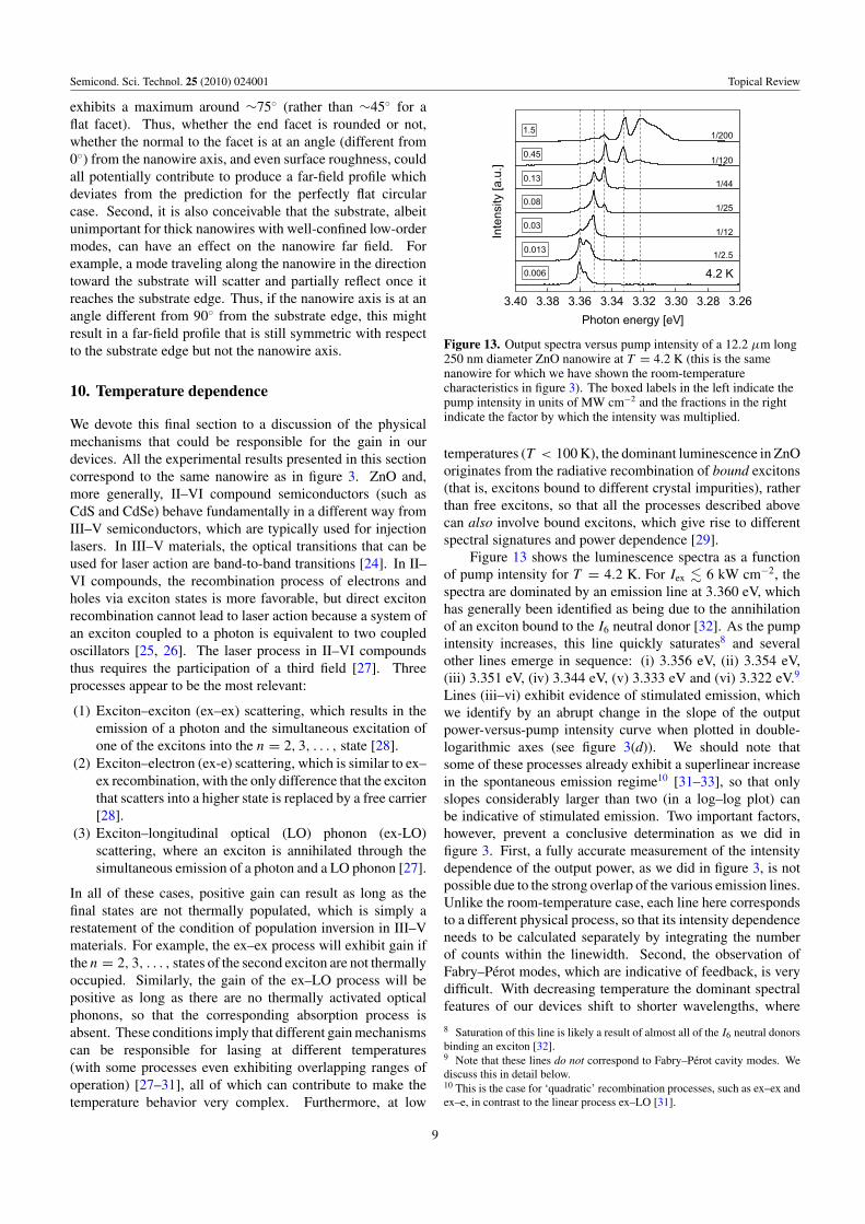
Figure 13. Output spectra versus pump intensity of a 12.2 μm long250 nm diameter ZnO nanowire at T = 4.2 K (this is the samenanowire for which we have shown the room-temperaturecharacteristics in figure 3). The boxed labels in the left indicate thepump intensity in units of MW cm−2 and the fractions in the rightindicate the factor by which the intensity was multiplied.
temperatures (T < 100 K), the dominant luminescence in ZnOoriginates from the radiative recombination of bound excitons(that is, excitons bound to different crystal impurities), ratherthan free excitons, so that all the processes described abovecan also involve bound excitons, which give rise to differentspectral signatures and power dependence [29].
Figure 13 shows the luminescence spectra as a functionof pump intensity for T = 4.2 K. For Iex � 6 kW cm−2, thespectra are dominated by an emission line at 3.360 eV, whichhas generally been identified as being due to the annihilationof an exciton bound to the I6 neutral donor [32]. As the pumpintensity increases, this line quickly saturates8 and severalother lines emerge in sequence: (i) 3.356 eV, (ii) 3.354 eV,(iii) 3.351 eV, (iv) 3.344 eV, (v) 3.333 eV and (vi) 3.322 eV.9
Lines (iii–vi) exhibit evidence of stimulated emission, whichwe identify by an abrupt change in the slope of the outputpower-versus-pump intensity curve when plotted in double-logarithmic axes (see figure 3(d)). We should note thatsome of these processes already exhibit a superlinear increasein the spontaneous emission regime10 [31–33], so that onlyslopes considerably larger than two (in a log–log plot) canbe indicative of stimulated emission. Two important factors,however, prevent a conclusive determination as we did infigure 3. First, a fully accurate measurement of the intensitydependence of the output power, as we did in figure 3, is notpossible due to the strong overlap of the various emission lines.Unlike the room-temperature case, each line here correspondsto a different physical process, so that its intensity dependenceneeds to be calculated separately by integrating the numberof counts within the linewidth. Second, the observation ofFabry–Perot modes, which are indicative of feedback, is verydifficult. With decreasing temperature the dominant spectralfeatures of our devices shift to shorter wavelengths, where
8 Saturation of this line is likely a result of almost all of the I6 neutral donorsbinding an exciton [32].9 Note that these lines do not correspond to Fabry–Perot cavity modes. Wediscuss this in detail below.10 This is the case for ‘quadratic’ recombination processes, such as ex–ex andex–e, in contrast to the linear process ex–LO [31].
9

Semicond. Sci. Technol. 25 (2010) 024001 Topical Review
Figure 14. Temperature dependence of the Fabry–Perot modespacing. The lines are plots of equation (1) for the electric fieldoriented perpendicular (E⊥C) and parallel (E‖C) to the crystalc-axis. The values for n were obtained from [34]. The filled circlescorrespond to the mode spacing obtained from measured spectra, asshown in figure 3(a).
the index of refraction of ZnO increases sharply [34]. Thepractical consequence of this is that the Fabry–Perot cavitymode spacing decreases and quickly falls below the resolutionof our apparatus, which is ∼0.2 nm. This is shown infigure 14, where we plot the calculated cavity mode spacing, asgiven by equation (1), as well as the experimentally observedvalues for 100 K < T < 290 K. When T < 100 K,the luminescence concentrates in the range 369 nm < λ <
372 nm, where the mode spacing is below our resolution (fora 12.2 μm long nanowire).
The spectra shown here are very similar to that reportedfor laser-excited ZnO platelets (at T = 1.2 K) by [32],who have interpreted these features as originating from theexcited states of the I6 donor. Such an assignment by meansof the emission energy alone is, unfortunately, not unique,given that different processes can have the same energy;for example, in [29] it was reported that the emission at3.322 eV can be due either to an ex–e process involving anexciton bound to a neutral donor or to an ex–ex collisionbetween free excitons. In fact, a thorough review of theliterature reveals that the exact emission characteristics ofZnO (and more generally II–VI semiconductors) depend onmany factors including the excitation method (laser [35] orelectron beam [36] irradiation), wavelength (one-photon ortwo-photon excitation [29]), pulse duration (longer pulses leadto heating and other effects [37]) as well as crystal qualityand preparation (such as whether the sample exhibits cleavedfacets or not [38]). Thus, while the exact identification ofthe mechanism (or mechanisms) responsible for lasing atlow temperatures (T < 100 K) is not possible by meansof the light emission wavelength alone, it is possible toconclude that these processes are exciton based, since theiremission energies (see figure 15) all lie >60 meV (that is, theexciton binding energy) below the bandgap of ZnO, which is≈3.44 eV at these temperatures [15].
We can provide some more insight into the generaltemperature behavior of these devices for T > 100 K, wherethe mechanism for lasing appears to be the same as at roomtemperature. As shown in figure 15, as the temperature
Figure 15. Temperature dependence of the peak energies ofspontaneous (×) and stimulated (•) emission of a 12.2 μm long250 nm diameter ZnO nanowire (this is the same nanowire forwhich we have shown the room temperature characteristics infigure 3 and the T = 4 K spectra in figure 13). The dash-dottedlines were taken from [39] and correspond to the photon energyvalues at which absorption in ZnO stays constant and given by thelabels (20 cm−1, 200 cm−1, 2000 cm−1). The other filled symbolsfor T > 100 K correspond the various stimulated emission linesobserved in figure 13.
increases past 100 K, the laser peak position shifts to lowerenergies much more rapidly than the spontaneous emission,where the latter can be related to the temperature variationof the bandgap. Note that the peak spontaneous emissionenergy does not correspond to the energy of the bandgap inZnO, but to an energy that is smaller by ≈60 meV, whichcorresponds to the exciton binding energy. The rate of shift is6.75 × 10−4 eV K−1, while the spontaneous emission variesat a rate of 3.92 × 10⁻⁴ eV K−1. This temperature behavioris surprising because it does not appear to coincide with thebehavior predicted for any particular process. For example, ifthe mechanism responsible for lasing at T > 100 K were theex–LO process, as some authors have suggested [29, 31, 36],the energy position would follow the relation [29]
hω = Eg(T ) − Eex − hωLO + 32kBT , (8)
where Eg(T ) is the bandgap energy, Eex is the exciton bindingenergy, hωLO is the energy of the LO phonon, and kB isthe Boltzmann constant. However, as seen in figure 15,the peak position shifts at a rate faster than is predicted bythis expression. This behavior has been observed before forZnO platelets and has been understood as due to temperaturebehavior of the absorption edge of ZnO [29, 37, 40]. Figure 15also shows the temperature dependence of the photon energyfor which absorption stays constant in ZnO, where we see thatthe temperature variation of the laser frequency agrees verywell with the position of constant absorption α = 20 cm−1.This behavior highlights an important distinction betweenIII–V lasers operating at the bandgap energy and II–VImaterials such as our ZnO devices [40]. For III–V lasers, thedominant absorption mechanism is intimately related to thegain mechanism, so that inverting the population to achievepositive gain eliminates the absorption process. In II–VImaterials, where the emission mechanism is exciton mediated,gain and loss are uncoupled. As we have already discussedabove, inverting the population in II–VI materials is equivalent
10
Semicond. Sci. Technol. 25 (2010) 024001 Topical Review
to the final states of the different gain processes not beingthermally populated. However, band edge absorption (or otherabsorption mechanisms) can still contribute to the loss and,therefore, strongly influence the operation of the laser. Fromwhat we have seen, the device attempts to maintain the lossat a constant value that is much smaller than the fixed cavitylosses (see figure 8).
11. Summary and conclusions
This paper has explored a wide array of topics relatedto laser oscillation in ZnO semiconductor nanowires bymeans of optical excitation. To begin, we presentedunambiguous evidence of laser action in ZnO nanowires,at room temperature, which was supported by a systematicstudy of the evolution of the various device properties fromASE to laser oscillation above threshold. More importantly,we demonstrated the key dependence of the laser thresholdon nanowire diameter, which we explored experimentallyand justified through a thorough theoretical study of theguided modes. Furthermore, we measured the angularand polarization properties of the far-field emission from ananowire laser. This measurement reinforced the conclusionsof our theoretical study of guided modes, strongly pointingto the TE01 and TM01 modes as those responsible for lasing.Finally, we also explored the behavior of our devices at lowtemperatures, from room temperature to 4.2 K, which suggeststhat the gain mechanism is exciton mediated. This studyhighlights several important differences in the operation of ourdevices (and more generally II–VI compound semiconductors)compared to standard III–V lasers. The work presented hereprovides the necessary tools to obtain a basic understandingof the physics and operation of these structures as well as theiroptimization and possible future incorporation in photoniccircuits.
Acknowledgments
We would like to thank C Borchers (University of Gottingen)for help in the TEM investigations. MAZ and FC weresupported by the National Science Foundation NanoscaleScience and Engineering Center (NSEC) under contractNSF/PHY 06-46094. The support of the Center for NanoscaleSystems (CNS) at Harvard University is also gratefullyacknowledged. Harvard-CNS is a member of the NationalNanotechnology Infrastructure Network (NNIN). SM andCR were supported by DFG-Project RO1198/7-3 within thepriority program SPP1125 nanowires.
References
[1] Huang M H, Mao S, Feick H, Yan H, Wu Y, Kind H, Weber E,Russo R and Yang P 2001 Room-temperature ultravioletnanowire nanolasers Science 292 1897–9
[2] Johnson J C, Yan H, Schaller R D, Haber L H, Saykally R Jand Yang P 2001 Single nanowire lasers J. Phys. Chem.B 105 11387–90
[3] Yu S F, Yuen C, Lau S P, Park W I and Yi G-C 2004 Randomlaser action in ZnO nanorod arrays embedded in ZnOepilayers Appl. Phys. Lett. 84 3241–3
[4] Hsu H-C, Wu C-Y and Hsieh W-F 2005 Stimulated emissionand lasing of random-growth oriented ZnO nanowiresJ. Appl. Phys. 97 064315
[5] Han X, Wang G, Wang Q, Cao L, Liu R, Zou B and Hou J G2005 Ultraviolet lasing and time-resolvedphotoluminescence of well-aligned ZnO nanorod arraysAppl. Phys. Lett. 86 223106
[6] Johnson J C, Choi H-J, Knutsen K P, Schaller R D, Yang P andSaykally R J 2002 Single gallium nitride nanowire lasersNature Mater. 1 106–10
[7] Duan X, Huang Y, Agarwal R and Lieber C M 2003Single-nanowire electrically driven lasers Nature421 241–5
[8] Agarwal R, Barrelet C J and Lieber C M 2005 Lasing in singlecadmium sulfide nanowire optical cavities Nano Lett.5 917–20
[9] Chin A H, Vaddiraju S, Maslov A V, Ning C Z, Sunkara M Kand Meyyappan M 2006 Near-infrared semiconductorsubwavelength-wire lasers Appl. Phys. Lett. 88 163115
[10] Siegman A E 1986 Lasers (Sausalito, CA: University ScienceBooks)
[11] Zimmler M A, Bao J, Capasso F, Muller S and Ronning C2008 Laser action in nanowires: observation of thetransition from amplified spontaneous emission to laseroscillation Appl. Phys. Lett. 93 051101
[12] Borchers C, Muller S, Stichtenoth D, Schwen D andRonning C 2006 Catalyst-nanostructure interaction in thegrowth of 1-D ZnO nanostructures J. Phys. Chem. B110 1656–60
[13] Wang Z L (ed) 2005 Nanowires and Nanobelts: Materials,Properties and Devices (Berlin: Springer)
[14] Casperson L W 1975 Threshold characteristics of multimodelaser oscillators J. Appl. Phys. 46 5194–201
[15] Madelung O (ed) 2003 Semiconductors: Data Handbook(Berlin: Springer)
[16] Maslov A V and Ning C Z 2003 Reflection of guided modes ina semiconductor nanowire laser Appl. Phys. Lett.83 1237–9
[17] Yariv A 1997 Optical Electronics in Modern Communications(Oxford Series in Electrical and Computer Engineering)(Oxford: Oxford University Press)
[18] Voss T, Svacha G T, Mazur E, Muller S, Ronning C,Konjhodzic D and Marlow F 2007 High-order waveguidemodes in ZnO nanowires Nano Lett. 7 3675–80
[19] Sullivan D M 2000 Electromagnetic Simulation Using theFDTD Method (New York: Wiley)
[20] Bhattacharya P 1997 Semiconductor Optoelectronic Devices(Upper Saddle River, NJ: Prentice-Hall)
[21] Maslov A V and Ning C Z 2004 Modal gain in asemiconductor nanowire laser with anisotropicbandstructure IEEE J. Quantum Electron. 40 1389–97
[22] Maslov A V and Ning C Z 2004 Far-field emission of asemiconductor nanowire laser Opt. Lett. 29 572–4
[23] Landau L D, Lifshitz E M and Pitaevskii L P 1984Electrodynamics of Continuous Media (Oxford:Butterworth-Heinenann)
[24] Chuang S L 1995 Physics of Optoelectronic Devices (NewYork: Wiley)
[25] Thomas D G and Hopfield J J 1962 Fluorescence in CdS andits possible use for an optical maser J. Appl. Phys.33 3243–9
[26] Haug H and Grob K 1967 Exciton laser theory Phys. Lett.A 26 41–2
[27] Haug H 1968 Theory of laser action involving free excitonsand LO-phonon-assisted transitions J. Appl. Phys.39 4687–95
[28] Haug H and Koch S 1977 On the theory of laser action indense exciton systems Phys. Status Solidi b 82 531–43
11
Semicond. Sci. Technol. 25 (2010) 024001 Topical Review
[29] Klingshirn C 1975 The luminescence of ZnO under high one-and two-quantum excitation Phys. Status Solidi b71 547–56
[30] Koch S W, Haug H, Schmieder G, Bohnert W andKlingshirn C 1978 Stimulated intrinsic recombinationprocesses in II–VI compounds Phys. Status Solidi b89 431–40
[31] Wunstel W and Klingshirn C 1980 Tunable laser-emissionfrom wurtzite-type II–VI compounds Opt. Commun.32 269–73
[32] Goto T and Langer D W 1971 Stimulated emission and excitedstates of the i6 donor electron in ZnO J. Appl. Phys.42 5066–71
[33] Hvam J M 1974 Exciton interaction in photoluminescencefrom ZnO Phys. Status Solidi b 63 511–7
[34] Park Y S and Schneider J R 1968 Index of refraction of ZnOJ. Appl. Phys. 39 3049–52
[35] Johnston W D Jr 1971 Characteristics of optically pumpedplatelet lasers of ZnO, CdS, CdSe, and CdS0.6Se0.4 between300◦ and 80◦K J. Appl. Phys. 42 2731–40
[36] Packard J R, Campbell D A and Tait W C 1967 Evidence forindirect annihilation of free excitons in II–VIsemiconductor lasers J. Appl. Phys. 38 5255–7
[37] Hvam J M 1971 Temperature-induced wavelength shift ofelectron-beam-pumped lasers from CdSe, CdS, and ZnOPhys. Rev. B 4 4459–64
[38] Nicoll F H 1966 Ultraviolet ZnO laser pumped by an electronbeam Appl. Phys. Lett. 9 13–5
[39] Jensen G Hvedstrup and Skettrup T 1973 Absorptionedge and Urbach’s rule in ZnO Phys. Status Solidi b60 169–73
[40] Leheny R F, Shaklee K L, Ippen E P, Nahory R E andShay J L 1970 A new model for the temperature-dependentCdS laser Appl. Phys. Lett. 17 494–7
12


![proc]_optically_pumped_mx... · strength is provided nowadays by quantum magnetometers based on the Zeeman effect in radio-¾xctra of nuclei and atoms. The optically pumped potassium](https://static.fdocuments.net/doc/165x107/5e480b8d7dbe47056e30b9f8/procopticallypumpedmx-strength-is-provided-nowadays-by-quantum-magnetometers.jpg)

![Lau, Stephan; Petković, Bojana; Haueisen, Jens · Magnetoresistive (MR) sensor technologies [4–8] as well as optically pumped magnetometer technologies [9–13] have reached sensitivities](https://static.fdocuments.net/doc/165x107/5d4cbc7c88c9932a0a8b7311/lau-stephan-petkovic-bojana-haueisen-jens-magnetoresistive-mr-sensor.jpg)