Optical Fiber to Waveguide Coupling Technique - apps.dtic.mil · Accer '77,r m l m mm-CONTENTS ......
15
Technical Report 1337 March 1990 Optical Fiber to Waveguide Coupling Technique N N D. J. Albares NOSC T. W. Trask San Diego State University Approved for public release: distribution Is unlimited.
-
Upload
nguyendien -
Category
Documents
-
view
220 -
download
2
Transcript of Optical Fiber to Waveguide Coupling Technique - apps.dtic.mil · Accer '77,r m l m mm-CONTENTS ......

Technical Report 1337March 1990
Optical Fiber toWaveguide CouplingTechnique
N
N D. J. AlbaresNOSC
T. W. TraskSan Diego State University
Approved for public release: distribution Is unlimited.

NAVAL OCEAN SYSTEMS CENTERSan Diego, California 92152-5000
J. D. FONTANA, CAPT, USN R. M. HILLYERCommander Technical Director
ADMINISTRATIVE INFORMATION
This work was performed at the Naval Ocean Systems Center by the Research andTechnology Branch, Code 553, and T. W. Trask, San Diego State University.
Released by Under authority ofR. E. Reedy, Head H. E. Rast, HeadResearch and Technology Solid State TechnologyBranch Division
JG
SUMMARY
This report investigated and demonstrated the feasibility of a technique for permanently coupling
optical fibers edge-on to thin-film waveguides.
The technique offers fine micropositioner adjustment via a needle vacuum chuck for maximum
optical coupling, offers robust mechanical support to the fibers from etched Si V-grooves, separates
the support and fine adjustment cementing steps to minimize curing and thermal stresses, relaxes the
requirements on fiber circularity and concentricity, is compatible with waveguide devices, and is suit-
able for close-spaced arrays of fibers.
Accer '77,r
m l m mm-

CONTENTS
INTRODUCTION ............................................................... 1I
BACKGROUND ................................................................ 2
COUPLING TECHNIQUE ........................................................ 3
EXPERIMENTS ................................................................ 4
REFERENCES ................................................................. 10
FIGURES
1. Fiber waveguide coupling schematic ............................................ 3
2. The needle vacuum chuck with a fiber ......................................... 4
3. V-groove etched in Si ...................................................... 5
4a. Single-fiber assembly showing V-groove upper left, fiber andwaveguide at lower right ................................................... 7
4b. Single-fiber assembly showing closeup of fiber and waveguide ...................... 7
5. Four-fiber assembly ........................................................ 8
6. Single-fiber assembly showing V-groove, fiber, and waveguide ....................... 9

INTRODUCTION
Emerging optical waveguide devices appear attractive as terminal elements in optical fiber transmis-sion, sensing, and signal processing applications. Such use naturally depends upon the permanentcoupling of single-mode optical fibers to channel thin-film waveguides, which is the subject of this pa-per. The purpose of this effort was to investigate a technique for optical fiber to channel waveguidecoupling, emphasizing suitability to different waveguide materials, stability, and producibility while be-ing compatible with methods to obtain maximum coupling efficiency and with waveguide device re-quirements such as electrical access.
Fiber coupling to thin-film waveguides can be done via evanescent wave coupling between the twowaveguides or by end-on launching. End-on coupling was chosen for its simplicity and its suitability todifferent waveguide materials. The approach conceived and developed here involves cementing thefibers in etched Si grooves with ultraviolet (UV)-curing adhesive for coarse positioning and mechanicalsupport. Subsequent fine positioning of a fiber is done with a needle vacuum chuck on a microma-nipulator followed by an final cementing step. Many fibers can be coupled to a waveguide chip facetwith this technique.
We investigated this technique experimentally, fabricating and testing three fiber-film assemblies.Single-mode optical fibers and thin-film channel waveguides in the 830-nm wavelength region wereused. We chose channel waveguides fabricated in LiNbO 3 by Ti indiffusion (Ti:LiNbO3 ), since theyare widely used for active and passive thin-film devices. We conclude that the coupling assemblyprocess is feasible and offers attractive features, including
* fine optical coupling adjustment separate from fiber support,
* optical coupling maximized from in situ transmission,
* minimized adhesive and thermai stress,
* suitability for different waveguide materials, and
* suitability for close-spaced fiber arrays.
Development of this technique would include further investigation of these features and how theyaffect attendant packaging and performance issues such as reliability, environmental effects,producibility, compatibility, and optical coupling efficiency.

BACKGROUND
In recent years, more research has been devoted to this subject (references 1 and 2), concentrat-ing on coupling efficiency in the end-on configuration, which is practical and not material specific.This efficiency is vital and clearly a challenge since the optical waveguides aie microns in size, modepatterns from two different types of waveguides must be matched, and film and fiber edge conditionsmust be controlled. The best figures reported for Ti:LiNbO 3 waveguides are 95% (-0.2 dB) couplingefficiency at X = 633 nm (reference 3) and a fiber waveguide fiber insertion loss of 1 dB for a1-cm-long waveguide at X = 1320 nm (reference 2). Micromanipulators were used to position thefibers in these experiments.
These figures exceed theoretical estimates for this coupling (reference 4), that involve calculation
of the overlap integral of the fiber and channel waveguide modes. The transverse fields of these opti-cal modes are modeled as circular and rectangular Gaussian functions respectively. Optimum condi-tions for coupling were calculated as well as the adverse effects of waveguide tilt, offset, and endseparation. For example, to keep each of these loss contributions below 10% (-0.5 dB) for typicalTi:LiNbO3 waveguides and fibers, the tilt should be less than about 1 degree, the offset less thanabout 0.8 im, and the end separation less than about 20 gm (references 1 and 5).
Although low-loss, adjustable connectors have been reported for fiber-film coupling, techniques forpermanent joining of many fibers to a thin-film waveguide chip are needed ultimately. The firstadjustable connector applied double eccentric cylindrical supports permitting the alignment of twosingle-mode waveguide components (reference 6). A second approach uses etched Si V-grooves forfiber positioning (reference 7), a flip-chip orientation for the thin film channel waveguides, andtapered fibers transverse to the coupling fibers for fine height adjustment (reference 8). These tech-niques appear limited to one or two fibers per chip facet.
Several approaches for attaching fibers permanently to LiNbO3 channel waveguides have beenimplemented in varying degrees. One coupler (reference 9) holds the fiber in place with a jigattached to the chip carrier. Fine adjustment is accomplished by set screws, and a final step of plas-tic molding fixes the fiber in place. This is not suitable for more than one or two fibers per chip edgeowing to the size of the positioning fixture.
Other techniques use Si V-grooves to support fibers in positions determined by photolithographicmasking and preferential chemical etching. The grooves can be defined to the same accuracy as thechannel waveguide lithography, and the etching has excellent control and reproducibility. In thisscheme, the accuracy of a fiber core position naturally depends upon the uniformity of the fiber outerdiameter (OD) and its concentricity with the core. Various methods are used for aligning the Si car-rier chip with the waveguide chip and, subsequently, cementing them.
One coupler (reference 10) uses etched V-grooves in Si for both fiber holding and as alignmentmarkers to bring the flip-chip LiNbO3 waveguides into proper registration before cementing. Fiberswere then placed in the grooves; permanent attachment was not reported. A second coupler (refer-ence 11) approach epoxies the fibers in the V-grooves and polishes the Si and fiber end surfaces flattogether. Then the Si chip is epoxied to a holder, which offers micrometer adjustment in the trans-verse directions after the epoxy has cured. An initial version had an external micropositioner, whichadjusted the Si chip into place and was removed after the epoxy step. However, this arrangementsuffered misalignment from stress placed on the Si chip by the curing epoxy.
A third example is a waveguide switch network coupled to four output fibers (reference 12).The fibers are sandwiched between two Si chips etched with V-grooves, and the chips are positioned
2

and epoxied to a mount carrying the switch chip. Mention was made of difficulty in epoxying the
fibers and Si chips for fine positioning, but details were not given.
To summarize, these methods for permanently attaching multiple fibers depend upon aligning
them relative to each other by their ODs using the very accurate Si V-grooves. Thus, the core loca-
tions depend upon the fiber qualities of uniformity and concentricity. The Si chip is then positioned
to align the V-grooves or the fibers in them with the channel waveguides and adhesive is applied to
fix positions. The chip positioning can be done well within the required accuracy but stress from the
curing epoxy causes misalignment. One approach retains fine adjustment, which is a disadvantage but
may be tolerated in certain applications.
COUPLING TECHNIQUE
The approach taken in this work is designed to retain the considerable advantage of Si V-groovesin supporting fiber arrays; retain fine micromanipulator final adjustment to accommodate imperfections
in fibers, V-grooves, and channel waveguide positions; and minimize stress from adhesive curing and
thermal changes. Figure 1 illustrates the concept. The fibers are completely supported by V-groovesin the Si chip, which is placed up to about 10 mm from the waveguide chip facet. The concept ismade attractive by the introduction of the needle vacuum chuck, which grasps each fiber providingmicromanipulator fine control to its alignment while it is cemented to the waveguide chip. Upon
maximization of light transmitted through the fiber waveguide assembly, UV light is applied to cure
the adhesive and the vacuum chuck is subsequently released. The V-groove alignment may be rela-tively coarse, <10 Am. The height is determined by the V-groove depth, the thickness of both chips,and the cement thickness between the chips and chip carrier. The transverse and angular alignmentof the V-grooves and waveguides can be done by bringing them into registration with a microscopefilar or by reference to chip edges, other grooves, or lithographic markers.
VACUUM NEEDLE WAEGUIDES
OPTICALFIBERS
SILICON CEMENT
CEMENT
Figure 1. Fiber waveguide coupling schematic.
There are two possible sequences for bonding the fibers, fixing the fiber end first or last. First a
fiber is placed in the V-groove, a small amount of adhesive is applied to just cover the fiber end face,
and the fiber is moved by the vacuum chuck into its final position where the adhesive fills the fiber-chip gap, of about 10 Aim. Adhesive is added to the V-groove surrounding the fiber, and UV light is
applied curing the adhesive in the gap and then in the grooves. In the second case, the fiber is
3

positioned in the V-groove and cemented. Then adhesive is applied to the fiber-chip gap and it iscured after fine alignment by the vacuum chuck. This has added flexibility in that fiber or fibers canbe cemented into a Si carrier and remain for an arbitrary curing period after which the final fiber endpositioning and cementing can be performed. The application of cement to the fiber-film gap requiresan extra step in this version. The cement can be applied to the gap itself, or the fiber can be raisedabove the waveguide chip by the vacuum chuck, exposing the fiber face for the application of cement.In either case, the technique for applying only the minimum amount of cement requires attention.
Therefore, by separating the V-groove fiber support from the fine-positioned fiber end by a dis-tance of 50 to 100 fiber diameters, stress of final fiber alignment and long-term cement curing at theV-grooves upon the fiber-waveguide coupling are minimized. Furthermore, applying the adhesive onlyto fill the fiber-chip gap minimizes any curing stress at that point, furnishes sufficient strength to main-tain the fiber in its fine-positioned place, and provides some index matching for the optical coupling.By using the small needle vacuum chuck, we are able to manipulate a fiber in a closely spaced array,cement it, and withdraw with no disturbance.
EXPERIMENTS
The experiments are described beginning with the components and their assembly and followed byresults and recommendations. The main elements are the needle vacuum chuck, the etched Si V-grooves, UV-curing optical cement, Ti:LiNbO3 channel waveguides, and the optical fibers. Theneedle vacuum chuck was adapted from one used for handling semiconductor chips. It had an OD of375 gim and inside diameter (ID) of 225 gim, shown in figure 2, and a groove was filed across a di-ameter to conform to the cylindrical shape of the fiber. A standard vacuum pump was attached viaflexible plastic tubing. The force exerted on the fiber was sufficient to lift it, although this is morethan is required for its positioning. Fibers can be spaced together down to the needle outer radiusplus the fine movement necessary for final positioning. For the needle, fiber, and typical adjustmentsused, this would amount to -325 gm fiber center-to-center spacing. Evidently there is room to reducethis figure through use of smaller needles and better V-groove-to-waveguide alignment.
Figure 2. The needle vacuum chuck with a fiber.
4

The Si V-grooves were etched in the usual way through a 1-gm-thick SiO 2 pattern fabricated by
photolithographic techniques. The etchant was KOH, and the chip had 100 orientation. Figure 3
shows the typical well-defined V-groove with its 70.5-degree vertex angle. The optical cement used
was Nor!and Optical Adhesive 61, a one-part liquid photopolymer that cures when exposed to UV
light. Characteristics reported by the manufacturer (reference 13) include good adhesion, low shrink-
age, flexibility, and n-1.5. It is usable in interferometric applicationb (reference 14). Using a UV
source of 1 mW/cm 2, we precured for about 2 minutes and cured for about 15 minutes.
Figure 3. V-groove etched in Si.
5

A Corning optical fiber was used with a 780-nm cutoff, 8-Mm core, and 1 2 5-tm OD. Attenuationwas quoted at 8.7 dB/km, and the plastic coating could be removed mechanically or with acetone.Fiber ends were cleaved by the well-known manual scribe and break method. The fiber end surfaceswere tested by an interferometer, which measured their flatness and perpendicularity to the fiber axis(reference 15).
Channel waveguides for the investigation were fabricated by Ti indiffusion in Z-cut LiNb0 3 2.0 cmlong. Widths ranged from 4 to 8 gm and their attenuation was estimated to be a few dB/cm, which ishigh compared with recent results (references 11 and 12). Conventional polishing techniques wereapplied to their entrance and exit facets to give nearly featureless edges under 600 X optical magnifi-cation (references 16 and 17). These waveguides supported a few modes at 633 nm and were singlemode at 830 nm.
The LiNb O 3 chip, the Si V-groove chip, and the optical fibers were assembled, supported by amicroscope slide chosen for experimental convenience. The LiNbO3 chip was cemented with thechannel waveguides positioned parallel to a reference edge on the microscope slide. A simple jig po-sitioned another reference edge parallel to the LiNbO 3 entrance facet so that the Si chip could slidealong it at the desired distance. Since the Si can be etched and cleaved along photolithographicallydefined lines, this allows us to maintain the grooves and channel waveguides parallel while slidingthem into transverse alignment. The Ti:LiNbO 3 waveguides are readily observable through a verticalillumination microscope due to the slight bulge created by the Ti indiffusion. In this alignment step,low magnification (10 X) was used to view a spot 2 cm in diameter, which included the V-grooves,the gap, and the waveguides. With a filar eyepiece, one could align the waveguides and the V-grooves to within a 10-gm offset. The Si chip was then cemented in place. Angular alignment is con-trolled by the assembly fixtures and is easily maintained to within a 1-degree deviation.
Accurate positioning of the fiber in the V-groove requires that it be stripped of its plastic buffercoating. The exposed fiber is weakened, and further support is needed where it emerges from the as-sembly. We provided a second, larger, in-line, V-groove section etched to hold, cemented, a 5- to10 mm-long coated length of the fiber. This gave a robust mechanical support that eliminated fiberbreakage after attachment and allowed handling of the completed assembly throughout the alignmentprocedures.
A drop of cement is applied just covering the fiber end, and the fiber is placed in the V-groovewhere it is grasped 1 to 2 mm from its end by the vacuum chuck. The fiber slides forward in theV-groove until the cement contacts the waveguide chip and the fiber end is within -10 gm of thechip. In the preferred sequence, cement is applied tc the V-groove and cured. The optical transmis-sion is then maximized by fine manipulation of the vacuum chuck, the end cement is cured, and thechuck is released. These techniques offer repeatability with a minimum of critical adjustments andadaptability to batch fabrication.
Three assemblies were made. Two were aligned with a 633-nm light, although the fiber cut-offwavelength was at 780 nm. One assembly had a single fiber, and the other had four fibers attachedas seen in figures 4 and 5. Loss measurements were made on the single-fiber assembly using the cut-back method. This technique involves launching light into the fiber and measuring the intensity trans-mitted through the assembly and emerging from the channel waveguide. Then without disturbing thelaunch conditions, one cuts the fiber and the intensity emerging from it is measured, yielding the inputintensity, which may then be compared to the transmitted intensity. This measurement at 633-nmwavelength yielded -1I dB loss.
6

Figure 4a. Single-fiber assembly showing V-groove upper left, fiber andwaveguide at lower right.
7-T
Figure 4b. Single-fiber assembly showing closeup 01 tiber and waveguicle.
7
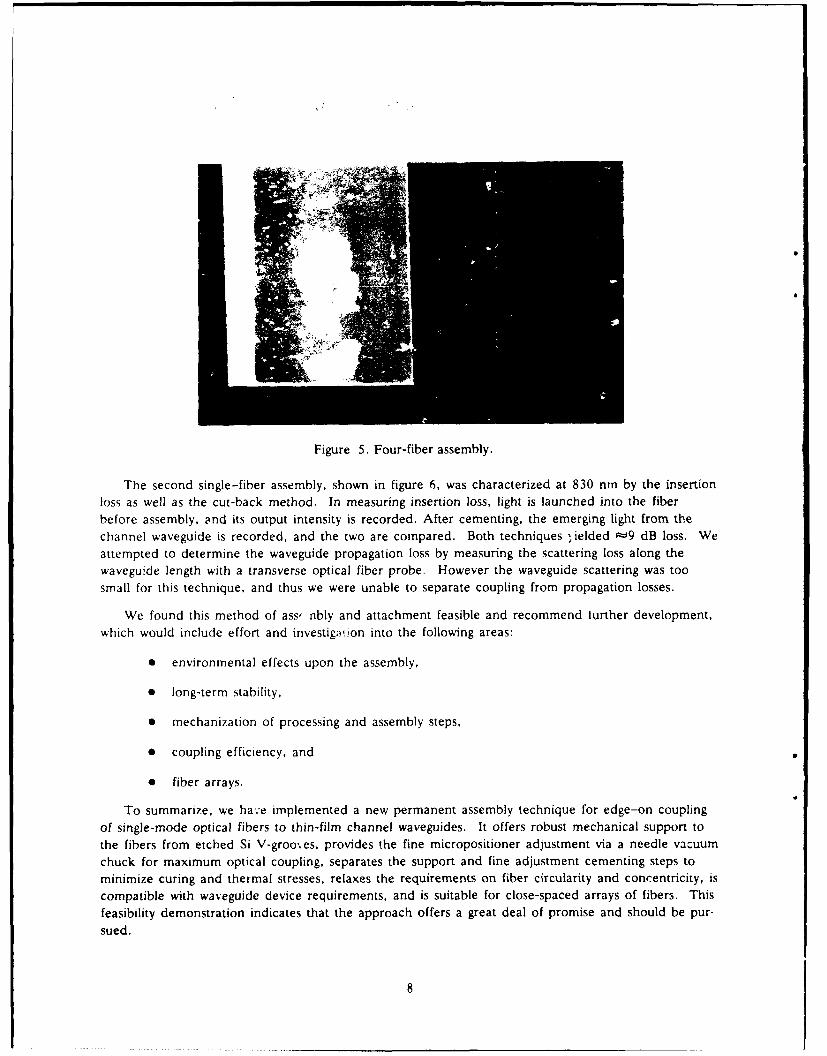
Figure 5. Four-fiber assembly.
The second single-fiber assembly, shown in figure 6, was characterized at 830 nm by the insertionloss as well as the cut-back method. In measuring insertion loss, light is launched into the fiberbefore assembly, and its output intensity is recorded. After cementing, the emerging light from thechannel waveguide is recorded, and the two are compared. Both techniques ,ielded -9 dB loss. Weattempted to determine the waveguide propagation loss by measuring the scattering loss along thewaveguide length with a transverse optical fiber probe. However the waveguide scattering was toosmall for this technique, and thus we were unable to separate coupling from propagation losses.
We found this method of ass, nbly and attachment feasible and recommend further development,which would include effort and investig;ion into the following areas:
* environmental effects upon the assembly,
* long-term stability,
* mechanization of processing and assembly steps,
* coupling efficiency, and
* fiber arrays.
To summarize, we have implemented a new permanent assembly technique for edge-on couplingof single-mode optical fibers to thin-film channel waveguides. It offers robust mechanical support tothe fibers from etched Si V-grooves, provides the fine micropositioner adjustment via a needle vacuumchuck for maximum optical coupling, separates the support and fine adjustment cementing steps tominimize curing and thermal stresses, relaxes the requirements on fiber circularity and concentricity, iscompatible with waveguide device requirements, and is suitable for close-spaced arrays of fibers. Thisfeasibility demonstration indicates that the approach offers a great deal of promise and should be pur-sued.
8

Figure 6. Single-fiber assembly showing V-groove, fiber and waveguide.
9

REFERENCES
1. Ramer, 0. G., 1981. "Single Mode Fiber-to-Channe. Waveguide Coupling," J. Opt. Comm. 2, 122.
2. Alferness, R. C., et al. 1982. "Efficient Single-Mode Fiber to Titanium Diffused Lithium NiobateWaveguide Coupling for X = 1.32 jim" IEEE J. Quantum Electron. QE-18, 1807.
3. Papuchon, M., P Kayoun, and Y. Bourbin 1982. High Coupling Efficiencies between Single ModeOptical Fibers and Ti Diffused LiNb0 3 Waveguides. Paper FB3-1, Topical Meeting on Integratedand Guided-Wave Optics, Pacific Grove, Calif., January 6-8.
4. Burns, W. K., and G. B. Hocker. 1977. "End Fire Coupling between Optical Fibers and DiffusedChannel Waveguides," Appl. Optics 16, 2048.
5. Ramer, 0. G. 1980, Controlled Fiber Optic Switching, Hughes Research Laboratory Air Force Techni-cal Report AFWAL-TR-81-1001.
6. Guttmann, J., 0. Krumpholz, and E. Pfeiffer. 1975. "Optical Fiber-Stripline-Coupler," Appl. Optics14, 1225.
7. Boivin, L. P. 1974. "Thin Film Laser to Fiber Coupler," Appl. Optics 13, 391.
8. Bulmer, C. H., et al. 1980. "High Efficiency Flip-Chip Coupling between Single-Mode Fibers andLiNbO 3 Channel Waveguides," Appl. Phys. Lett. 37, 351.
9. Noda, J., et al. 1978. "Single-Mode Optical Waveguide Fiber Coupler," Appl. Optics 17, 2092.
10. Hsu, H. P., A. F. Milton, and W. K. Burns. 1978. "Multiple Fiber End Fire Coupling with Single-Mode Channel Waveguides," Appl. Phys. Lett. 33, 603.
11. Ramer, 0. G., C. Nelson, and C. Mohr. 1981. "Experimental Integrated Optic Circuit Losses andFiber Pigtailing of Chips," IEEE J. Quantum Electron. QE-17, 970.
12. Kondo, M. et al. 1982. "Integrated Optical Switch Matrix for Single-Mode Fiber Networks," IEEEJ. Quantum Electron. QE-18, 1759.
13. Norland Products, Inc., Box 145, North Brunswick, N.J. 08902.
14. Wimpers, J. R., and S. F. Johnston. 1984. "Optical Cements for Interferometric Applications," Appl.Optics 23, 1145.
15. Gordon, K. S. et al. 1977. "Fiber-Break Testing by Interferometry; a Comparison of TwoBreaking Methods," Appl. Optics 16, 818.
16. Schumacher, E. R. 1980. "Defect-Free Edge Polishing of Lithium Niobate and Other Optical Crys-tals," NOSC TR 480.
17. Furch, B. et al. 1983. "Fast High-Quality Edge Polishing of LiNbO3 ," J. Opt. Commun. 4, 47.
10

Public reporting burden for this collection of intotmaton Is estimated to averag I hour par respona. Wklud n tkie for revieng Inatnidkons. searching existing data sources, gatheringand maintaining the data needed. aind comnpleiting and rwevieng the colilectIon of InfonnaItn SeOnd on regarding Ofs burden estitele or any other aspect of this collection of Informa-tion. Including suggestionsa foeducing this burden, to Washington Headquarters Sevicee. Dlrediorele for InilormtImh Opertions and Reports, 1215 Jefferson Davis Highway. Sts 1204,
I. AENC US ONL (Lom " 2.REPRT ATE3 REPORT TYPE AND DATES COVERED
I Marc 1990Final
4 TITE ANSUBITLE5. FUNDING NUMBERS
OPTICAL FIBER TO WAVEGUIDE COUPLING TECHNIQUE P.E. 0602301E_____________________________________________________ DN: 388650
D. J. Albares, NOSCT. W. Trask, S. D. S. U
7 PERFORMING ORGANIZATION NAME(S) AND ADDRESS(ES) 8 PERFORMING ORGANIZATIONREPMR NUMBER
Naval Ocean Systems Center NOSC TR 1337San Diego, CA 92152-5W0
9 SPONSORING/MONITORING AGENCY NAME(S) ANC) ADDRESS(ES) 10, SPONSORING/MONITORiNGAGENCY REPORT NUMBER
11 SUPPLEMENTARY NOTES
12& DISTRIBUTIONJAVAILABIUTY STATEMENT 12b DISTIBI11ON CODE
Approved for public release; distribution is unlimited.
13 ABSTRACT (MaxJnurn 200 wordts)
A technique for permanently coupling optical fibers edge-on to thin-film waveguides was investigated and its feasibilitydemonstrated. It offers the fine micropositioner adjustment via a needle vacuum chuck for maximum optical coupling, offersrobust mechanical support to the fibers from etched Si V-grooves, separates the support and fine adjustment cementing stepsto minimize curing and thermal stresses, relaxes the requirements on fiber circularity and concentricity, is compatible withwaveguide devices, and is suitable for close-spaced arrays of fibers.
14. SUBJECT TERMS 15. NUMBER OF PAGES
thin-film 1channel waveguides 16 PRCCDoptical fiber coupling
17 SECURITY CLASSIFICATION 18! SECURITY CLASSIFICATION IQ SECURTY CLASSIFICATION 20. UMITATION Or ABISTRACTOF REPORT OF TM11 PAGE OF ABSTRACT
UNCLASSIFIED UNCLASSIFIED UNCLASSIFIED SAME AS REPORT
NSN 7540-01-24=~5( Standard tornm 298