Operations Manual - Illunis Manual RMV-71 RMOD-71 RMV-71/RMOD-71 Operations Copyright illunis, LLC...
106
Rugged Machine Vision Advanced Digital Machine Vision Cameras Operations Manual RMV-71 RMOD-71
Transcript of Operations Manual - Illunis Manual RMV-71 RMOD-71 RMV-71/RMOD-71 Operations Copyright illunis, LLC...
Rugged M
achin
e V
isio
n
A
dvan
ced
Dig
ital M
ach
ine V
isio
n C
am
eras
Operations Manual
RMV-71 RMOD-71

RMV-71/RMOD-71 Operations Copyright illunis, LLC 7/8/2016 Page 2
Specia
l N
ote
s
Ru
gg
ed
Mach
ine V
isio
n
Welcome to the illunis RMV-71/RMOD-71 Digital Cam-era Users Manual. Our goal is to provide the best pos-sible documentation for the RMV-71/RMOD-71 camera; therefore, illunis will update this document with your feedback. illunis welcomes comments and criticism of this document. This document specifically covers the CMOS RMV-71/RMOD-71 Camera Link camera. Please direct your comments to: [email protected].
Corporate Address illunis, LLC 14700 Excelsior Boulevard Minnetonka, MN USA Zip Code: 55345 Phone: (952) 975.9203 Fax: (952) 294.8308 Internet Web: www.illunis.com Email: [email protected] Owners Dave Krekelberg: [email protected] Scott Elhardt: [email protected]
Specifications subject to change without notice.
RMV-71/RMOD-71 Operations Copyright illunis, LLC 7/8/2016 Page 3
RMV-71/RMOD-71 Release Notes
Thank you for purchasing the RMV-71/RMOD-71 digital camera from illunis. These cameras use the latest technology, which includes Camera Link (CL) and USB-3 with the following notes: RMV-71/RMOD-71 camera supports the output raster of the 10,000 x 7094 sensor array.
Limitations due to capture card memory mapping may restrict the maximum raster output. RMV-71/RMOD-71 camera supports calibration features which include:
Column offset balancing for the sensors internal 16 column bus. Black level setting for the analog front end. Column gain for the entire array.
Note: Calibration will require optical set up that involves dark and bright fields. The specification for the pixel clock of the CHR-71M is 30Mhz. This mode is provided for
compatibility with the specification and to provide a lower clock speed to allow longer cam-era link cables
For ultimate performance, the fundamental limitation is the maximum Camera Link data
rate of 85Mhz. This limits the maximum pixel clock speed to 42.5Mhz, which is provided as an overclock mode. Operation is guaranteed at 30Mhz pixel clock and below.
POCL cables are compatible with the RMV-71/RMOD-71 camera. POCL mode is currently
not available.
RMV-71/RMOD-71 Operations Copyright illunis, LLC 7/8/2016 Page 4
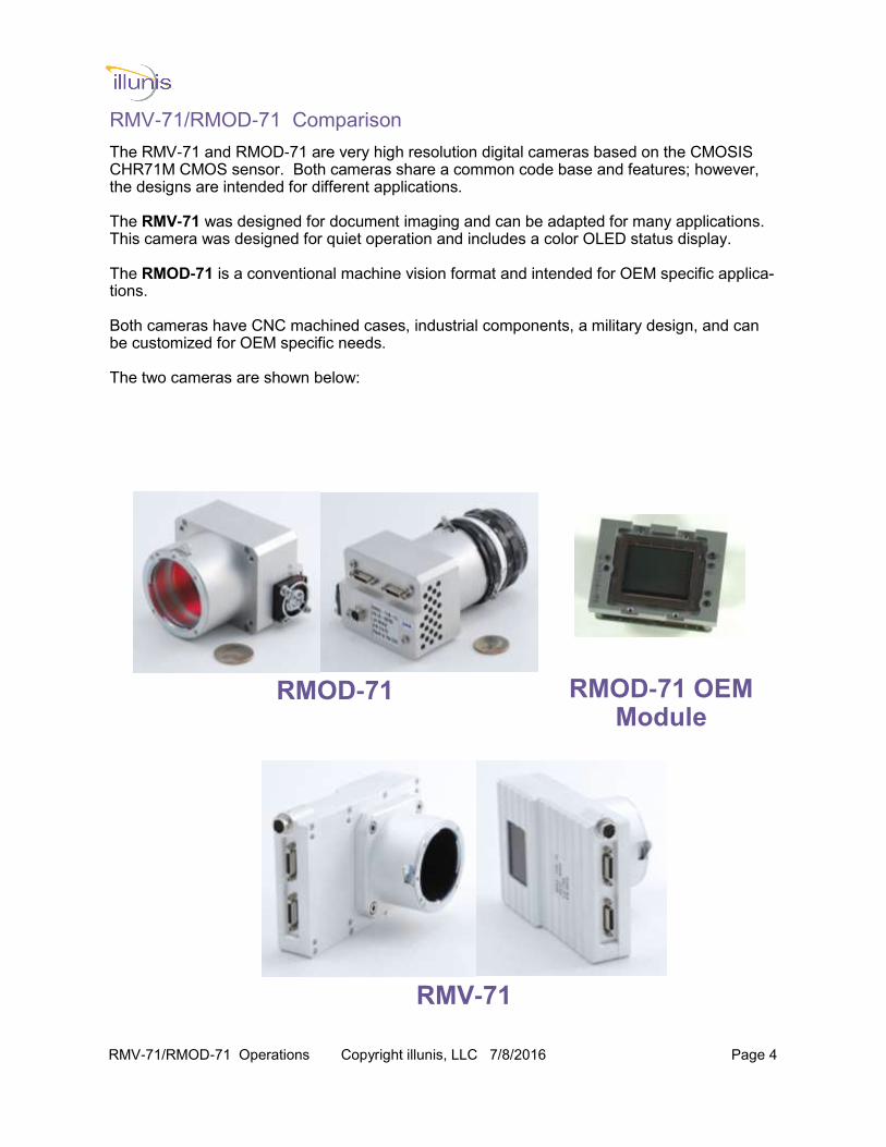
RMOD-71
RMV-71
RMV-71/RMOD-71 Comparison
The RMV-71 and RMOD-71 are very high resolution digital cameras based on the CMOSIS CHR71M CMOS sensor. Both cameras share a common code base and features; however, the designs are intended for different applications. The RMV-71 was designed for document imaging and can be adapted for many applications. This camera was designed for quiet operation and includes a color OLED status display. The RMOD-71 is a conventional machine vision format and intended for OEM specific applica-tions. Both cameras have CNC machined cases, industrial components, a military design, and can be customized for OEM specific needs. The two cameras are shown below:
RMOD-71 OEM Module

RMV-71/RMOD-71 Operations Copyright illunis, LLC 7/8/2016 Page 5
The RMV-71 was the first camera designed by illunis using the CHR71M sensor from CMOSIS. This camera was designed for the document imaging market and its form factor. The RMV-71 is built in OLED status display, which lends itself to this type of application. The RMOD-71 is a redesign of the RMV-71 in a more conventional machine vision form factor. The heart of the RMOD-71 is a simple, small, board “module” that incorporates the sensor, electronics, and a 3-point mount for sensor alignment. This module is designed to allow arrays of sensors to be built; thus, providing the foundation for future super high resolution camera arrays of a Gigapixel or more! The RMOD-71 TEC Cooled is designed to provide active cooling from a small long life fan. This fan cools the camera sensor and electronics to near ambient and minimizes dark current in long exposures. In addition, the RMOD-71 TEC Cooled has the ability to sequence the CHR71M sensor in custom modes, which provides special trigger and mechanical shutter modes.
Feature RMV-71 RMOD-71 Benefit
Design 1st Generation 2nd Generation Newer
Target Markets Document Imaging Machine Vision, Aerial Imaging, LCD/PCB inspection
Sensor CMOSIS CHR71M CMOSIS CHR71M Same
Data output Camera Link Base & Medium, USB3
Camera Link Base & Medium, USB3
Same
Max Power 6.5W 4.5W 30% less
OLED status display Yes No
Non Uniformity Correction Yes, Each Mode Yes, Each Mode
Operating Temp Ambient + 20C Ambient + 4C Runs cooler
Hot pixels at 2500ms, max temp
11.63% 1.9% 6x Less dark current
Max FPS full resolution 4.22 fps 4.22 fps Same !
Sensor 3Pt Mounted Yes Yes Same !
Built In Fan No (for quiet operation) Yes Runs Cooler
Mechanical Shutter No Option Global shutter operation.
Size 82x120x32mm 72x60x42mm Lens mount not included
Weight 530grams (18.8oz) 360grams (12.7oz)
RMV-71/RMOD-71 Operations Copyright illunis, LLC 7/8/2016 Page 6
RMV-71/RMOD-71 Document Revisions
RMV-71/RMOD-71 Precautions Do not drop, damage, disassemble, immerse, repair, or alter the camera. Do not apply incorrect power. Applying incorrect power may damage the camera. Do not open the housing of the camera. The warranty becomes void if the camera is
opened or modified in any way not approved by illunis. Please direct any questions or problems to: [email protected].
Issue Date Modification
1 11-5-13 Original Document.
2 Clean up of ‘0x’ hex variables in tables. Updated Mode1 register. Updated Accelerometer orientation XYZ G readout.
3 11-20-13 Added Flat Field Correction Instructions.
5 05-19-14 Updated Temp Range to match sensor spec.
6 06-12-14 Updated power connector part number.
7 06-30-14 Updated QE Curves with color and added angular response.
8 12-2-14 New format. Added sensor defect specification. Added Firmware/State save/restore to file instructions. Added Long Exposure information. New firmware for: Hot pixel correction. Triggered flash/strobe/shutter operation. Extended pixel defect correction to 8191 pixels. Several minor bugs fixed. FPGA F0.51, Micro F0.53, and GUI control program 3.0.1 are required.
9 12-16-14 Added # hot pixels corrected. Updated Firmware/State save/restore for TriggeredFlash Added readout mode on OLED and detector OSD FPGA F0.52, Micro F0.56, and GUI control program 3.0.1 are required.
10 11-3-15 RMOD added
RMV-71/RMOD-71 Operations Copyright illunis, LLC 7/8/2016 Page 7
Quic
k S
tart
Guid
e
R
ug
ged
Mach
ine V
isio
n
RMV-71/RMOD-71 Quick Start:
The RMV-71/RMOD-71 is a Camera Link device that needs: 6-12V DC Power to the Hirose 6 pin connector. Base Mode or Medium Mode Camera Link capture card (Coreco PX4 and Matrox Helios have been tested). One or two Camera Link cables (Mini HDR to SDR) rated at
85Mhz or more (two cables for Medium Format). F-Mount lens. illunis Camera Control Software (GUI). Download at: http://illunis.com. This RMV-71/RMOD-71 manual. How to start imaging with the RMV-71/RMOD-71: Install capture card and software. Install illunis Camera Control Software (GUI). Unpack the RMV-71/RMOD-71 and install the lens. Connect the RMV-71/RMOD-71 power cable. Make sure
the DC ground of the power cable is the same as the DC ground of the capture card (PC). If they are not similar, a “ground loop” may occur and could damage the camera !
Connect the RMV-71/RMOD-71 Camera Link cables (see
page 26). Note: When looking from the front/lens, the left connector is base and the right connector is medium.
Power the RMV-71/RMOD-71. The OLED display will show
the boot sequence and display information about the camera configuration. Run the capture card application to begin imaging. Run illunis Camera Control Software (GUI) to change camera settings.
RMV-71/RMOD-71 Operations Copyright illunis, LLC 7/8/2016 Page 8
RMV-71/RMOD-71 Quick Start Continued:
RMV-71/RMOD-71 features to explore: 71 Megapixels at 4.2 fps, equates to 340 Megapixels per second at 12 bits
per pixel, 4G bit/sec. Readout window size and position can be manipulated. Changing the size will
increase the frame rate. Readout window can be set to HD-4K at ~30 fps ! (see page 11).
Image exposure can be set to a time longer than readout. This will slow the
readout and the effective frames per second. Camera can be triggered from the Camera Link or the external power cable. Camera requires dark field and bright field image calibration to eliminate sensor
column artifacts. On-Screen and OLED displays show vital information about camera operation. Digital gain and offset, as well as histogram equalization is provided for quick
image setup. Exposures are set in line times. The smaller the line the shorter the exposure. Capture card can be used to flip or rotate the image. All allowable pixel, column and row defects are correct within the camera. Hot pixel correction is available for long exposures.
Please read the following manual and send your comments to: [email protected].
RMV-71/RMOD-71 Operations Copyright illunis, LLC 7/8/2016 Page 9
Table
Of Conte
nts
R
ug
ged
Mach
ine V
isio
n 1 RMV-71/RMOD-71
Overview 2 Hardware 3 Software ICD 4 Image Exposure 5 Image Processing 6 Image Detectors 7 On-Screen Displays 8 Camera Link 9 FAQ’s
RMV-71/RMOD-71 Operations Copyright illunis, LLC 7/8/2016 Page 10
Chapte
r 1:
Overv
iew
Ru
gg
ed
Mach
ine V
isio
n
The RMV-71/RMOD-71 Digital Camera incorporates the CMO-SIS CHR71M-sensor. Sensor Features
10,000 x 7096 active pixels with a 3.1µm pitch. Frame rate at full resolution is 4 frames /sec. Windowing capability in 16 x 8 pixel increments. Moving window capability. Selectable pixel clock from two sources (30, 42.5Mhz). 8 analog outputs digitized to 12 bits. On chip timing for Free Run and Trigger Modes. Mono or Bayer pattern output. Mono is available with (Std.) or without micro lenses.
Sensor Specifications
Full well charge: > 13ke. Sensitivity: 0.15A/W (@ 555nm). Dark Noise: 7e- Conversion factor: ~63uv/e. Dynamic range: 64dB. Dark Current: 3.2e-/s @ room temperature. Fixed Pattern noise: 0.09 (% of full swing).
Camera Features
Data output in Camera Link Base or Medium Format. Frame rates to maximum Camera Link data speed (85Mhz). 3-point mounted sensor in CNC machined case. F-Mount lens is standard. Other mounts available. Color and monochrome sensors supported. Internal defect correction for Pixels, Rows, and Columns.
1.0: RMV-71/RMOD-71 Overview
RMV-71/RMOD-71 Operations Copyright illunis, LLC 7/8/2016 Page 11
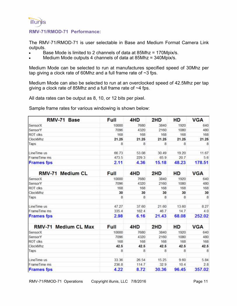
RMV-71/RMOD-71 Performance:
The RMV-71/RMOD-71 is user selectable in Base and Medium Format Camera Link outputs. Base Mode is limited to 2 channels of data at 85Mhz = 170Mpix/s. Medium Mode outputs 4 channels of data at 85Mhz = 340Mpix/s. Medium Mode can be selected to run at manufactures specified speed of 30Mhz per tap giving a clock rate of 60Mhz and a full frame rate of ~3 fps. Medium Mode can also be selected to run at an overclocked speed of 42.5Mhz per tap giving a clock rate of 85Mhz and a full frame rate of ~4 fps. All data rates can be output as 8, 10, or 12 bits per pixel. Sample frame rates for various windowing is shown below:
RMV-71/RMOD-71 Operations Copyright illunis, LLC 7/8/2016 Page 12
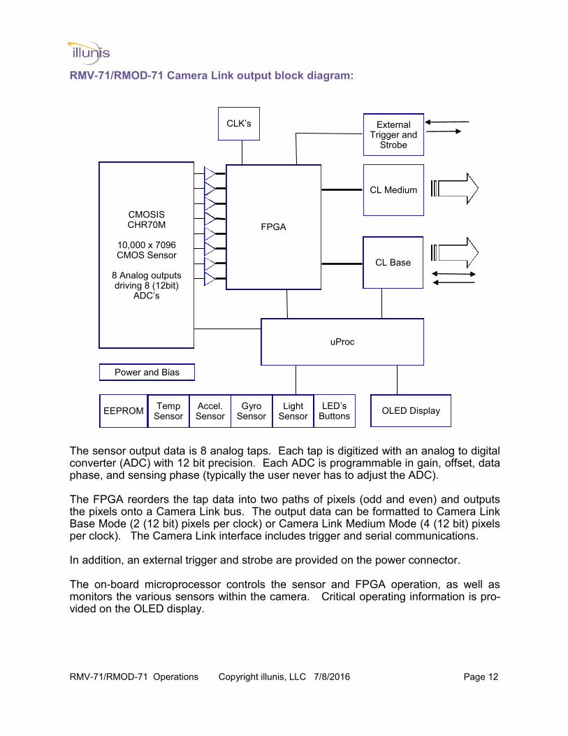
RMV-71/RMOD-71 Camera Link output block diagram:
CMOSIS CHR70M
10,000 x 7096 CMOS Sensor
8 Analog outputs driving 8 (12bit)
ADC’s
FPGA
uProc
CL Medium
Accel. Sensor
Temp Sensor
CL Base
Gyro Sensor
Light Sensor
Power and Bias
External Trigger and
Strobe
EEPROM OLED Display LED’s
Buttons
CLK’s
The sensor output data is 8 analog taps. Each tap is digitized with an analog to digital converter (ADC) with 12 bit precision. Each ADC is programmable in gain, offset, data phase, and sensing phase (typically the user never has to adjust the ADC). The FPGA reorders the tap data into two paths of pixels (odd and even) and outputs the pixels onto a Camera Link bus. The output data can be formatted to Camera Link Base Mode (2 (12 bit) pixels per clock) or Camera Link Medium Mode (4 (12 bit) pixels per clock). The Camera Link interface includes trigger and serial communications. In addition, an external trigger and strobe are provided on the power connector. The on-board microprocessor controls the sensor and FPGA operation, as well as monitors the various sensors within the camera. Critical operating information is pro-vided on the OLED display.

RMV-71/RMOD-71 Operations Copyright illunis, LLC 7/8/2016 Page 13
RMV-71/RMOD-71 Operations Copyright illunis, LLC 7/8/2016 Page 14
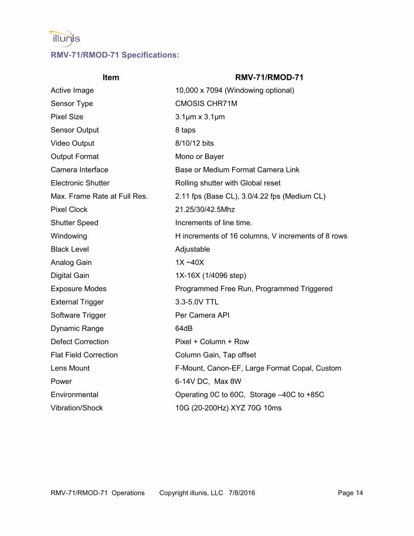
RMV-71/RMOD-71 Specifications:
Item RMV-71/RMOD-71
Active Image 10,000 x 7094 (Windowing optional)
Sensor Type CMOSIS CHR71M
Pixel Size 3.1µm x 3.1µm
Sensor Output 8 taps
Video Output 8/10/12 bits
Output Format Mono or Bayer
Camera Interface Base or Medium Format Camera Link
Electronic Shutter Rolling shutter with Global reset
Max. Frame Rate at Full Res. 2.11 fps (Base CL), 3.0/4.22 fps (Medium CL)
Pixel Clock 21.25/30/42.5Mhz
Shutter Speed Increments of line time.
Windowing H increments of 16 columns, V increments of 8 rows
Black Level Adjustable
Analog Gain 1X ~40X
Digital Gain 1X-16X (1/4096 step)
Exposure Modes Programmed Free Run, Programmed Triggered
External Trigger 3.3-5.0V TTL
Software Trigger Per Camera API
Dynamic Range 64dB
Defect Correction Pixel + Column + Row
Flat Field Correction Column Gain, Tap offset
Lens Mount F-Mount, Canon-EF, Large Format Copal, Custom
Power 6-14V DC, Max 8W
Environmental Operating 0C to 60C, Storage –40C to +85C
Vibration/Shock 10G (20-200Hz) XYZ 70G 10ms
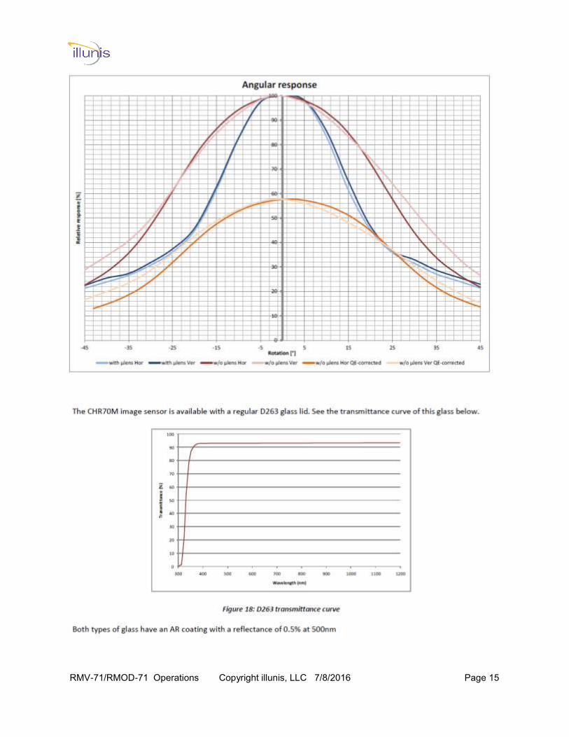
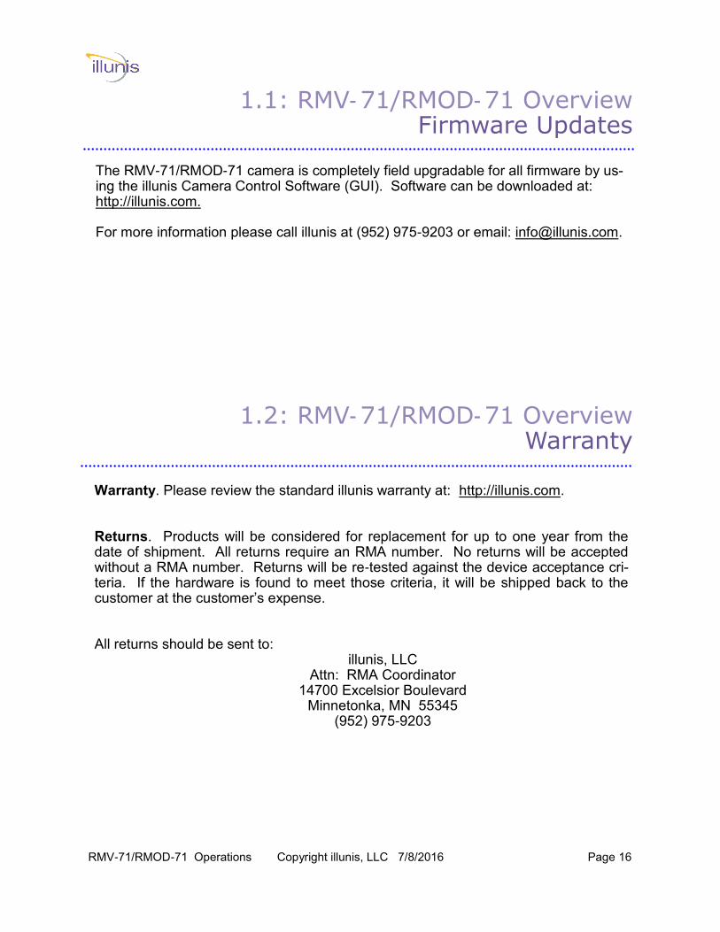
RMV-71/RMOD-71 Operations Copyright illunis, LLC 7/8/2016 Page 15
RMV-71/RMOD-71 Operations Copyright illunis, LLC 7/8/2016 Page 16
The RMV-71/RMOD-71 camera is completely field upgradable for all firmware by us-ing the illunis Camera Control Software (GUI). Software can be downloaded at: http://illunis.com.
For more information please call illunis at (952) 975-9203 or email: [email protected].
1.1: RMV-71/RMOD-71 Overview Firmware Updates
1.2: RMV-71/RMOD-71 Overview Warranty
Warranty. Please review the standard illunis warranty at: http://illunis.com. Returns. Products will be considered for replacement for up to one year from the date of shipment. All returns require an RMA number. No returns will be accepted without a RMA number. Returns will be re-tested against the device acceptance cri-teria. If the hardware is found to meet those criteria, it will be shipped back to the customer at the customer’s expense. All returns should be sent to:
illunis, LLC Attn: RMA Coordinator
14700 Excelsior Boulevard Minnetonka, MN 55345
(952) 975-9203
RMV-71/RMOD-71 Operations Copyright illunis, LLC 7/8/2016 Page 17
1.3: RMV-71/RMOD-71 Overview Compliance
The RMV-71/RMOD-71 camera is tested to comply with the following: FCC-A
1.4: RMV-71/RMOD-71 Overview Power Consumption
The RMV-71/RMOD-71 camera can operate in the following modes with estimated power: Base Mode at 20Mhz pixel clock = ~4.4W @ 12VDC. Medium Mode at 30Mhz pixel clock = ~5.4W at 12VDC. Medium Mode at 40Mhz pixel clock = ~6.4W at 12VDC. All measurements are at full readout (10,000 x 7096). Note: At lower input voltage the power draw is slightly higher.
1.4: RMV-71/RMOD-71 Overview Sensor Defects
The RMV-71/RMOD-71 camera uses the CMOSIS CHR71M sensor. This sensor can have the following maximum allowable defects: FPN: Max 1% RMS PRNU : Max 5% RMS Defective Columns: 15* Defective Rows: 15* Defective Pixels: 5000 Clusters: 0** *No adjacent column or row defects are allowed. **Clusters are allowed as long as pixels are correctable (pixels which have a minimum of 2 vertical, horizontal, or diag-onal non-defect neighbors. A high-grade sensor is available at a higher cost. Please contact: [email protected].

RMV-71/RMOD-71 Operations Copyright illunis, LLC 7/8/2016 Page 18
Chapte
r 2:
Hard
ware
Ru
gg
ed
Mach
ine V
isio
n
2.0 Hardware Overview 2.1 CAD Models 2.2 Power Connector 2.3.1 Power Cable Drawings 2.3.2 Camera Link Cables
2.4 Optional Tripod Mount 2.5 Considerations 2.6 Options 2.7 Optics & Lens Considerations 2.8 Display & LED’s
RMV-71/RMOD-71 Operations Copyright illunis, LLC 7/8/2016 Page 19
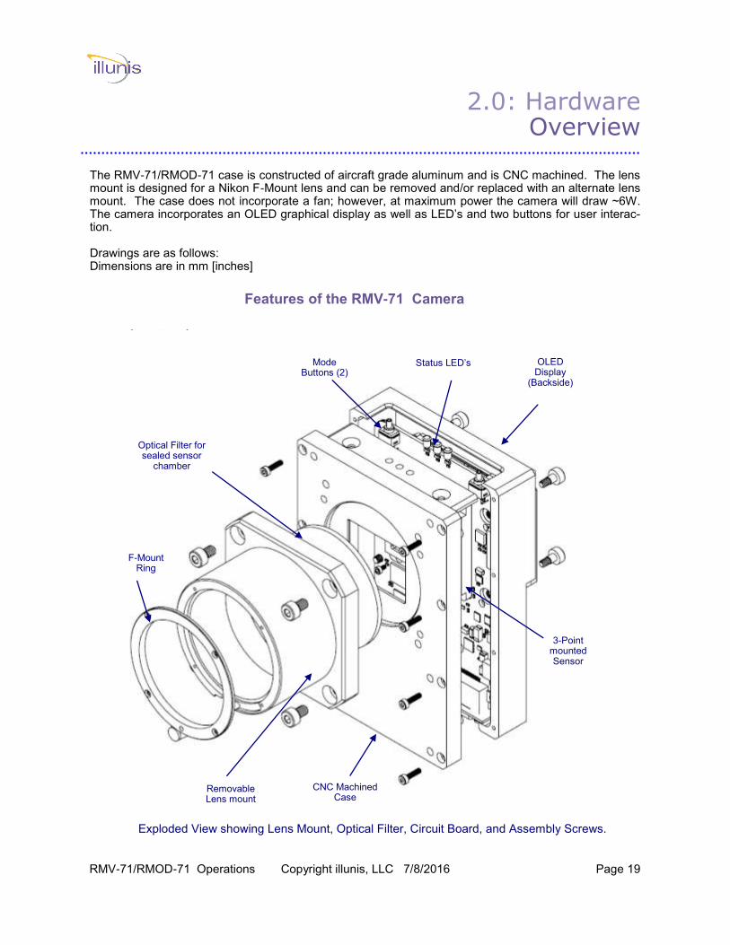
2.0: Hardware Overview
Features of the RMV-71 Camera
Exploded View showing Lens Mount, Optical Filter, Circuit Board, and Assembly Screws.
The RMV-71/RMOD-71 case is constructed of aircraft grade aluminum and is CNC machined. The lens mount is designed for a Nikon F-Mount lens and can be removed and/or replaced with an alternate lens mount. The case does not incorporate a fan; however, at maximum power the camera will draw ~6W. The camera incorporates an OLED graphical display as well as LED’s and two buttons for user interac-tion. Drawings are as follows: Dimensions are in mm [inches]
F-Mount Ring
Optical Filter for sealed sensor
chamber
Removable Lens mount
CNC Machined Case
Status LED’s OLED Display
(Backside)
Mode Buttons (2)
3-Point mounted Sensor
RMV-71/RMOD-71 Operations Copyright illunis, LLC 7/8/2016 Page 20
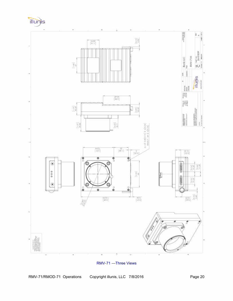
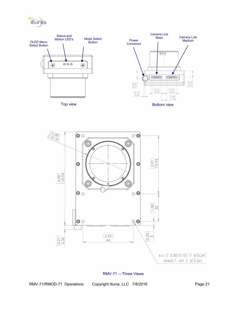
RMV-71 —Three Views
RMV-71/RMOD-71 Operations Copyright illunis, LLC 7/8/2016 Page 21
Top view Bottom view
OLED Menu Select Button
Status and Motion LED’s Mode Select
Button Power
Connector
Camera Link Base Camera Link
Medium
RMV-71 —Three Views

RMV-71/RMOD-71 Operations Copyright illunis, LLC 7/8/2016 Page 22
Features of the RMOD-71 Camera Note: An OEM version is available without the lens mount
Exploded View showing Lens Mount, Optical Filter, Circuit Board, and Assembly Screws.
F-Mount Ring
Optical Filter for sealed sensor
chamber
Lens mount
CNC Machined Case
Status LED’s
3-Point mounted Sensor
Cooling Fan
Power Connector +12V, GND
Trigger, Strobe
Camera Link Base
Camera Link Medium
RMOD-71 Cable Connections
RMV-71/RMOD-71 Operations Copyright illunis, LLC 7/8/2016 Page 23
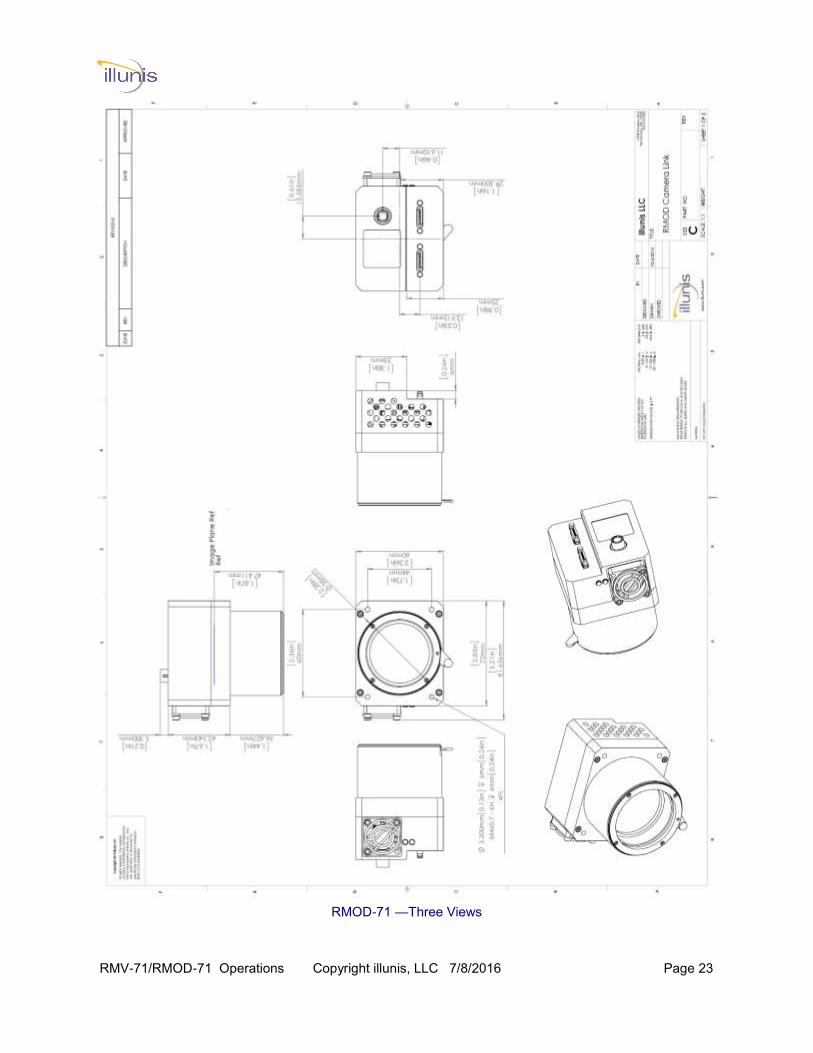
RMOD-71 —Three Views
RMV-71/RMOD-71 Operations Copyright illunis, LLC 7/8/2016 Page 24
CAD Models: Detailed Drawings The RMV-71/RMOD-71 case dimensions can be provided as manufacturing drawings and as a solid model that can be imported into almost any CAD system. For access to these drawings, please contact illunis at: (952) 975-9203 or email: [email protected]. CAD Models supported are STEP, IGES, ProE native, and many others.
2.1: Hardware CAD Models
HR
S
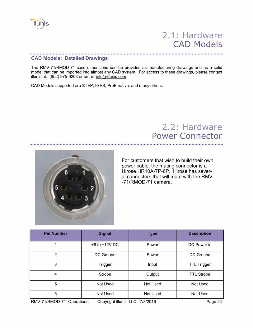
2.2: Hardware Power Connector
Pin Number Signal Type Description
1 +6 to +12V DC Power DC Power in
2 DC Ground Power DC Ground
3 Trigger Input TTL Trigger
4 Strobe Output TTL Strobe
5 Not Used Not Used Not Used
6 Not Used Not Used Not Used
For customers that wish to build their own power cable, the mating connector is a Hirose HR10A-7P-6P. Hirose has sever-al connectors that will mate with the RMV-71/RMOD-71 camera.
RMV-71/RMOD-71 Operations Copyright illunis, LLC 7/8/2016 Page 25
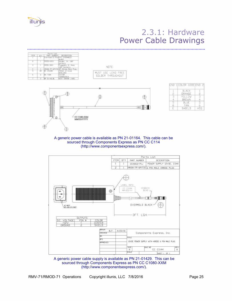
2.3.1: Hardware Power Cable Drawings
A generic power cable is available as PN 21-01164. This cable can be sourced through Components Express as PN CC C114
(http://www.componentsexpress.com/).
A generic power cable supply is available as PN 21-01429. This can be sourced through Components Express as PN CC C1080-XXM
(http://www.componentsexpress.com/).
RMV-71/RMOD-71 Operations Copyright illunis, LLC 7/8/2016 Page 26
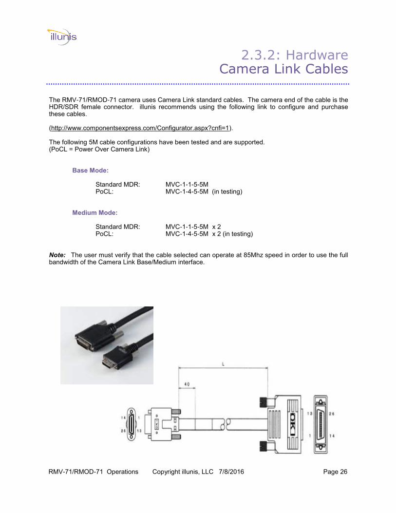
2.3.2: Hardware Camera Link Cables
The RMV-71/RMOD-71 camera uses Camera Link standard cables. The camera end of the cable is the HDR/SDR female connector. illunis recommends using the following link to configure and purchase these cables. (http://www.componentsexpress.com/Configurator.aspx?cnfi=1). The following 5M cable configurations have been tested and are supported. (PoCL = Power Over Camera Link) Base Mode: Standard MDR: MVC-1-1-5-5M PoCL: MVC-1-4-5-5M (in testing) Medium Mode: Standard MDR: MVC-1-1-5-5M x 2 PoCL: MVC-1-4-5-5M x 2 (in testing) Note: The user must verify that the cable selected can operate at 85Mhz speed in order to use the full bandwidth of the Camera Link Base/Medium interface.

RMV-71/RMOD-71 Operations Copyright illunis, LLC 7/8/2016 Page 27
2.4 Hardware Optional Tripod Mount
An optional tripod mounting brack-et is available for the RMV-71: illunis PN 26-01816.
RMV-71/RMOD-71 Operations Copyright illunis, LLC 7/8/2016 Page 28
2.5: Hardware Considerations
● Do not open or disassemble the camera case or electronics as there are no user adjustments within the camera. This will void the warrantee. ● Care must be taken in handling as not to create static discharge that may permanently damage the device. ● Do not apply power with reversed polarity as this may render the camera non-functional and will void the warrantee. ● Camera Link is a DC based interface. The camera and capture device must share the same electrical ground. Failure to do so will destroy the Camera Link interface chips and/or camera and capture card. Absolute Maximum Ratings Input Voltage: 6 to 16V DC Storage Temperature: -40C to +70C
Recommended Maximum Ratings Input Voltage: 6 to 14V DC Operating Temperature: 0C to +60C Most illunis cameras operate beyond these temperature limits, please call for details.
Recommended Operating Conditions Input Voltage: 7-12V DC Operating Temperature: 0C to 60 Relative humidity should not exceed 80% non-condensing.
Thermal Interface The RMV-71/RMOD-71 camera contains many advanced circuits and performs at high clock speeds and thus requires careful consideration for thermal cooling. The camera should be used either with a lens and/or a solid mechanical mount that acts as a heat sink.
Power Consumption The RMV-71/RMOD-71 camera was designed to be as small as possible and as such has a high ener-gy density. The various operating modes of the RMV-71/RMOD-71 will change the power consump-tion from the base line. In particular, the binning and partial scan modes require more power. The Triggered Modes are lowest in power when the camera is waiting for a trigger. Special versions of the RMV-71/RMOD-71 with lower clock speeds are available with lower power consumption. Special Notes for “Rugged” Environmental Use The RMV-71/RMOD-71 cameras are designed using military 0.6 stress ratings on all passive compo-nents and uses industrial temperature range active components when ever possible. The RMV-71/RMOD-71 is assembled using standard commercial techniques that DO NOT HARDEN the mechani-cal components against vibration. illunis highly recommends that any use of the RMV-71/RMOD-71 in any application that requires high vibration and extreme temperature ranges has the hardware in-spected and modified using adhesives to retain the mechanical components.
RMV-71/RMOD-71 Operations Copyright illunis, LLC 7/8/2016 Page 29
2.6: Hardware Options
The RMV-71/RMOD-71 can be customized with the following: Case Options: Without the F-Mount lens for OEM use. Without the case as a bare PCB for OEM use. Lens Mount Options: No lens mount (as above). Canon EF lens mount and controller from Birger engineering (Provides focus and IRIS control of many Canon lenses). Large format lens using custom Copal-0 Mount (Provides integrated mechanical shutter and IRIS). Custom designed lens mount (please contact illunis). Sensor Options: RGB Bayer with micro lens, D263 AR Coated Cover Glass. Mono with micro lens, D263 AR Coated Cover Glass. Mono without micro lens, D263 AR Coated Cover Glass. Other Options: Tripod mount. Over-clocking. Mechanical shutter and IRIS. Custom features. For option availability contact: [email protected] .

RMV-71/RMOD-71 Operations Copyright illunis, LLC 7/8/2016 Page 30
2.7: Hardware Optics and Lens Considerations
The CMOSIS CHR71M sensor is slightly smaller than the standard 35mm format. The CHR71M has a diagonal of 38mm vs the 43.3mm diagonal of the 35mm format. This results in an increase in effective focal length of 43.3/38 = 1.14X.
Thus, a 50mm focal length lens for a 35mm camera will have an effective 57mm focal length.
Full Frame 35mm format sensor (36x24mm)
CHR71M sensor (31x22mm)
The CMOSIS CHR71M sensor pixel size is small for a large sensor at 3.1um pitch. This presents a challenge for the selection of a lens. Some of the best lenses that illunis has tested are from Schneider and Edmund optics: 50mm F2.2 P# 1062672 http://www.schneiderkreuznach.com/fileadmin/user_upload/bu_industrial_solutions/industrieoptik/Unifoc_Lenses/Einlegeblatt_Tabelle_Large_Format_Sensoren_engl_fuer_web.pdf http://www.edmundoptics.com/imaging/imaging-lenses/techspec-lenses/large-format-fixed-focal-length-lenses/3518 Other lenses to consider: http://www.edmundoptics.com/imaging/imaging-lenses/techspec-lenses/high-resolution-large-format-lenses/3339
RMV-71/RMOD-71 Operations Copyright illunis, LLC 7/8/2016 Page 31
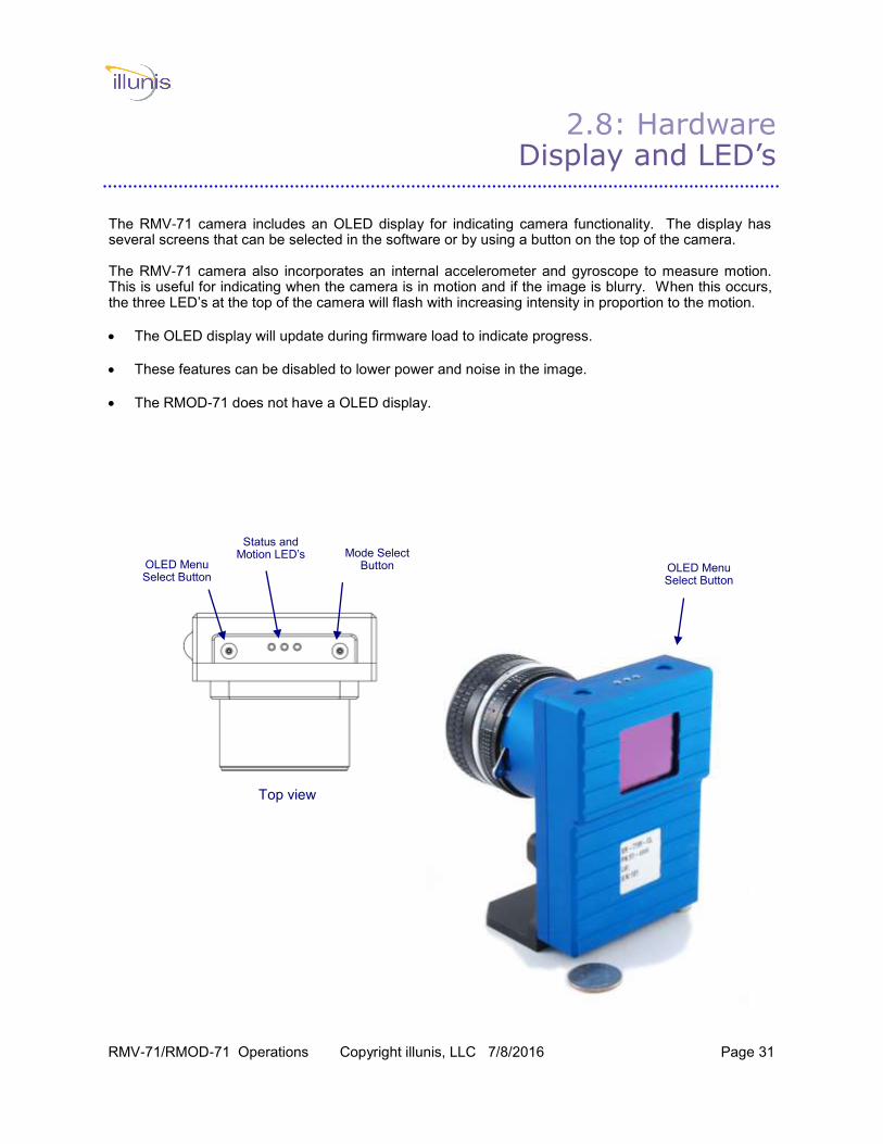
2.8: Hardware Display and LED’s
The RMV-71 camera includes an OLED display for indicating camera functionality. The display has several screens that can be selected in the software or by using a button on the top of the camera. The RMV-71 camera also incorporates an internal accelerometer and gyroscope to measure motion. This is useful for indicating when the camera is in motion and if the image is blurry. When this occurs, the three LED’s at the top of the camera will flash with increasing intensity in proportion to the motion.
The OLED display will update during firmware load to indicate progress.
These features can be disabled to lower power and noise in the image.
The RMOD-71 does not have a OLED display.
Top view
OLED Menu Select Button
Status and Motion LED’s Mode Select
Button OLED Menu Select Button

RMV-71/RMOD-71 Operations Copyright illunis, LLC 7/8/2016 Page 32
Chapte
r 3:
Soft
ware
ICD
R
ug
ged
Mach
ine V
isio
n
3.0 Software Overview 3.1 Serial Interface 3.2 Command Packets 3.3 Command Table 3.4 System & Status 3.5 Baud Rate 3.6 Graphical User Interface 3.7 Camera Update/Backup
RMV-71/RMOD-71 Operations Copyright illunis, LLC 7/8/2016 Page 33
3.0: Software ICD Overview
3.1: Software ICD Serial Interface
SERIAL INTERFACE PROTOCOL Implementation Camera communication is accomplished via asynchronous serial communication according to EIA Standard RS 232 C through the Camera Link cable. Data rate: Full Duplex, 9600 baud.
1 START bit.
8 DATA bits – The LSB (D0) is transfered first.
1 STOP bit.
No parity.
The RMV-71/RMOD-71 software interface (commonly called an Inter-Connect-Description or ICD) was developed for high reliability applications. The ICD incorporates error checking and a handshake proto-col, which responds with either a positive or negative acknowledge signal. The communication path from frame grabber to the RMV-71/RMOD-71 is through the Camera Link cable. The Camera Link com-mittee has specified that devices connected must first communicate at 9600 baud. This default baud rate is slow for devices such as the RMV-71/RMOD-71 camera; therefore, the RMV-71/RMOD-71 has a selectable baud rate for faster communication speeds. The RMV-71/RMOD-71 microprocessor is a flash programmable device with many features vital to the operation of the RMV-71/RMOD-71 camera. Some of these features include:
Hardware UART used for serial communications.
A watchdog timer used to monitor communication errors and system faults.
Onboard RAM and EEPROM for saving camera settings.
Parallel data bus for high speed interfaces to the FPGA and NAND FLASH memories.
Brown out detection and reset.
Camera Capture Device
Command with checksum
Data and/or ACK/NACK

RMV-71/RMOD-71 Operations Copyright illunis, LLC 7/8/2016 Page 34
3.2: Software ICD Command Packets
Protocol
The RMV-71/RMOD-71 camera is controlled through command packets. The RMV-71/RMOD-71 camera is considered a slave device and never generates data without a read request. The data packet formatting is described in detail below. Note: the checksum is calculated only on the 4 ascii characters comprising the Data.
Data Packets Data packets are of either ‘read’ or ‘write’ types. For example: to read the camera serial number, the packet sent to the camera would be {r07000002fe}. The camera would respond by issuing an acknowledge character ! followed by the response {r0700sssscc}, where ssss is the camera serial number and cc is the checksum calculated in hex as 0x0100 – ( ss (high byte hex) + ss (low byte).
Packet Format 1 Char 2 Char 2 Char 2 Char 4 Char 2 Char 1 Char 1 Char
Start Command Target Index Data Checksum End Ack/Nack
Start: Indicates the Start of the frame
Size = 1 ascii character Value = 123 Decimal (ascii { ) Command:
Command descriptor Size = 1 ascii character Value = 114 Decimal (ascii r ) for Read Value = 119 Decimal (ascii w ) for Write Target:
Command descriptor Size = 2 ascii characters Index:
Command descriptor Size = 2 ascii characters Data:
The data transferred Size = 4 ascii characters Checksum of Data only (default) Size = 2 ascii characters - Intel-Standard - two’s compliment of sum of data.
Example 1: Data = 2002, checksum = lower byte of (0x100 – (0x20 + 0x02)) = 0xde Example 2: Data = 0000, checksum = lower byte of (0x100 – (0x00 + 0x00)) = 0x00
Example 3: Data = fef0, checksum = lower byte of (0x100 – (0xfe + 0xf0)) = 0x12
Checksum of Command and Data: checksum( comandindex ) + checksum( data)
Example 4: Command = 0400, data = 0x0001 (0x100 – (0x04 + 0x00)) = 0xFC
(0x100—(0x00 + 0x01)) = 0xFF Checksum = lower byte of 0xFC + 0xFF => 0xFB End Indicates the End of the frame Size = 1 ascii character Value = 125 Decimal (ascii } )
Ack/Nack
Positive acknowledge - Negative acknowledge Size = 1 ascii character Ack Value = 33 Decimal (ascii ! )
Nack Value = 63 Decimal (ascii ? )
COMMAND DESCRIPTIONS Read Command Structure The RMV-71/RMOD-71 camera parses the sequence byte by byte. An invalid read command, target , or index will cause the camera to issue a NACK. The Host (the user) will generate dummy data with a valid checksum then an end. The camera will respond with an ACK and re-send the command with valid data and checksum. If the Host detects an error, it will re-issue the command. Host {r tt ii 0 0 0 0 cc}, camera issues ! Camera issues {r tt ii data data data data cc} (NOTE no ACK).
Write Command Structure The RMV-71/RMOD-71 camera parses the sequence byte by byte. An invalid write command, target, index, or checksum will cause the camera to issue a NACK; otherwise, the write
sequence will complete and the camera will issue an ACK after the command has been executed. The camera receives the checksum from the Host. Host {w tt ii data data data data cc} camera issues !
Error Checking The RMV-71/RMOD-71 camera parser is character by charac-ter and will respond with an immediate NACK if any unrecog-nized command, target, index, or checksum occurs.
Communication Timeouts The RMV-71/RMOD-71 camera micro-controller uses a hard-ware watchdog timer that will time out if the time between bytes are longer than ???ms. When sending command frames to the camera, the Host must not have significant delays between bytes sent.
RMV-71/RMOD-71 Operations Copyright illunis, LLC 7/8/2016 Page 35
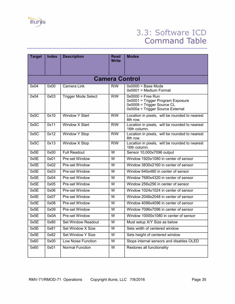
3.3: Software ICD Command Table
Target Index Description Read Write
Modes
Camera Control 0x04 0x00 Camera Link R/W 0x0000 = Base Mode
0x0001 = Medium Format
0x04 0x03 Trigger Mode Select R/W 0x0000 = Free Run 0x0001 = Trigger Program Exposure 0x0009 = Trigger Source CL 0x000a = Trigger Source External
0x5C 0x10 Window Y Start R/W Location in pixels, will be rounded to nearest 8th row.
0x5C 0x11 Window X Start R/W Location in pixels, will be rounded to nearest 16th column.
0x5C 0x12 Window Y Stop R/W Location in pixels, will be rounded to nearest 8th row.
0x5C 0x13 Window X Stop R/W Location in pixels, will be rounded to nearest 16th column.
0x5E 0x00 Full Readout W Sensor 10,000x7096 output
0x5E 0x01 Pre-set Window W Window 1920x1080 in center of sensor
0x5E 0x02 Pre-set Window W Window 3830x2160 in center of sensor
0x5E 0x03 Pre-set Window W Window 640x480 in center of sensor
0x5E 0x04 Pre-set Window W Window 7680x4320 in center of sensor
0x5E 0x05 Pre-set Window W Window 256x256 in center of sensor
0x5E 0x06 Pre-set Window W Window 1024x1024 in center of sensor
0x5E 0x07 Pre-set Window W Window 2048x2048 in center of sensor
0x5E 0x08 Pre-set Window W Window 4096x4096 in center of sensor
0x5E 0x09 Pre-set Window W Window 7096x7096 in center of sensor
0x5E 0x0A Pre-set Window W Window 10000x1080 in center of sensor
0x5E 0x80 Set Window Readout W Must setup X/Y Size as below
0x5E 0x81 Set Window X Size W Sets width of centered window
0x5E 0x82 Set Window Y Size W Sets height of centered window
0x60 0x00 Low Noise Function W Stops internal sensors and disables OLED
0x60 0x01 Normal Function W Restores all functionality
RMV-71/RMOD-71 Operations Copyright illunis, LLC 7/8/2016 Page 36
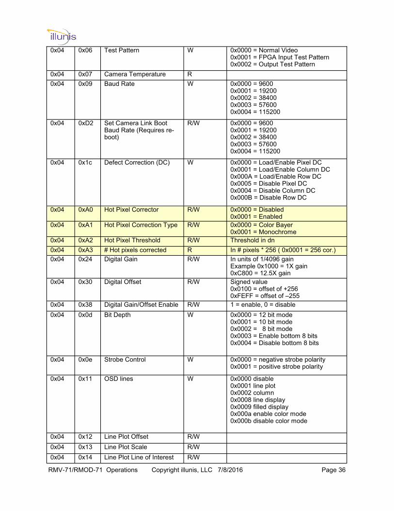
0x04 0x06 Test Pattern
W 0x0000 = Normal Video 0x0001 = FPGA Input Test Pattern 0x0002 = Output Test Pattern
0x04 0x07 Camera Temperature R
0x04 0x09 Baud Rate W 0x0000 = 9600 0x0001 = 19200 0x0002 = 38400 0x0003 = 57600 0x0004 = 115200
0x04 0xD2 Set Camera Link Boot Baud Rate (Requires re-boot)
R/W 0x0000 = 9600 0x0001 = 19200 0x0002 = 38400 0x0003 = 57600 0x0004 = 115200
0x04 0x1c Defect Correction (DC) W 0x0000 = Load/Enable Pixel DC 0x0001 = Load/Enable Column DC 0x000A = Load/Enable Row DC 0x0005 = Disable Pixel DC 0x0004 = Disable Column DC 0x000B = Disable Row DC
0x04 0xA0 Hot Pixel Corrector R/W 0x0000 = Disabled 0x0001 = Enabled
0x04 0xA1 Hot Pixel Correction Type R/W 0x0000 = Color Bayer 0x0001 = Monochrome
0x04 0xA2 Hot Pixel Threshold R/W Threshold in dn
0x04 0xA3 # Hot pixels corrected R In # pixels * 256 ( 0x0001 = 256 cor.)
0x04 0x24 Digital Gain R/W In units of 1/4096 gain Example 0x1000 = 1X gain 0xC800 = 12.5X gain
0x04 0x30 Digital Offset R/W Signed value 0x0100 = offset of +256 0xFEFF = offset of –255
0x04 0x38 Digital Gain/Offset Enable R/W 1 = enable, 0 = disable
0x04 0x0d Bit Depth W 0x0000 = 12 bit mode 0x0001 = 10 bit mode 0x0002 = 8 bit mode 0x0003 = Enable bottom 8 bits 0x0004 = Disable bottom 8 bits
0x04 0x0e Strobe Control
W 0x0000 = negative strobe polarity 0x0001 = positive strobe polarity
0x04 0x11 OSD lines W 0x0000 disable 0x0001 line plot 0x0002 column 0x0008 line display 0x0009 filled display 0x000a enable color mode 0x000b disable color mode
0x04 0x12 Line Plot Offset R/W
0x04 0x13 Line Plot Scale R/W
0x04 0x14 Line Plot Line of Interest R/W
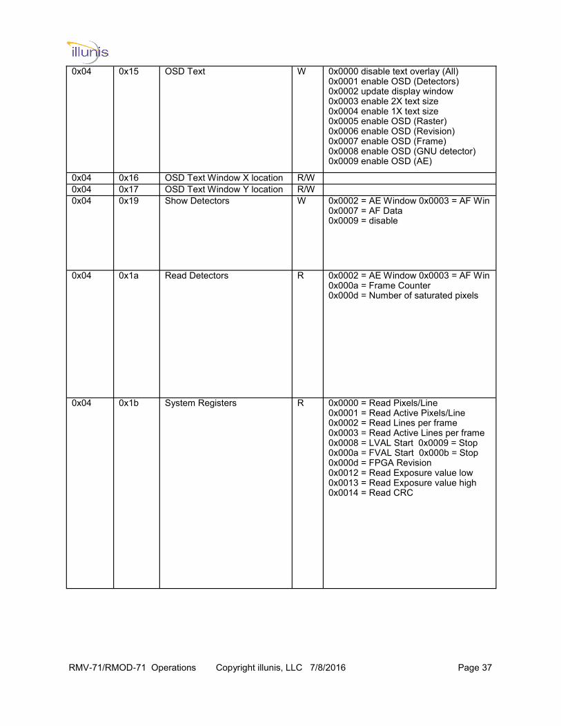
RMV-71/RMOD-71 Operations Copyright illunis, LLC 7/8/2016 Page 37
0x04 0x15 OSD Text W 0x0000 disable text overlay (All) 0x0001 enable OSD (Detectors) 0x0002 update display window 0x0003 enable 2X text size 0x0004 enable 1X text size 0x0005 enable OSD (Raster) 0x0006 enable OSD (Revision) 0x0007 enable OSD (Frame) 0x0008 enable OSD (GNU detector) 0x0009 enable OSD (AE)
0x04 0x16 OSD Text Window X location R/W
0x04 0x17 OSD Text Window Y location R/W
0x04 0x19 Show Detectors W 0x0002 = AE Window 0x0003 = AF Win 0x0007 = AF Data 0x0009 = disable
0x04 0x1a Read Detectors R 0x0002 = AE Window 0x0003 = AF Win 0x000a = Frame Counter 0x000d = Number of saturated pixels
0x04 0x1b System Registers R 0x0000 = Read Pixels/Line 0x0001 = Read Active Pixels/Line 0x0002 = Read Lines per frame 0x0003 = Read Active Lines per frame 0x0008 = LVAL Start 0x0009 = Stop 0x000a = FVAL Start 0x000b = Stop 0x000d = FPGA Revision 0x0012 = Read Exposure value low 0x0013 = Read Exposure value high 0x0014 = Read CRC
RMV-71/RMOD-71 Operations Copyright illunis, LLC 7/8/2016 Page 38
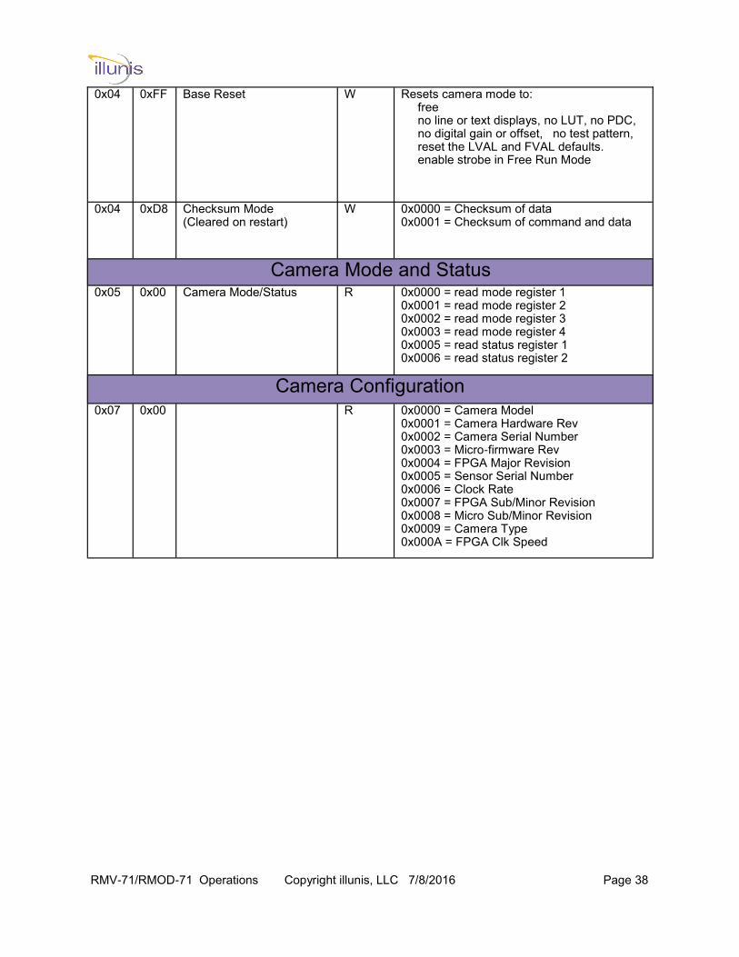
0x04 0xFF Base Reset W Resets camera mode to: free no line or text displays, no LUT, no PDC, no digital gain or offset, no test pattern, reset the LVAL and FVAL defaults. enable strobe in Free Run Mode
0x04 0xD8 Checksum Mode (Cleared on restart)
W 0x0000 = Checksum of data 0x0001 = Checksum of command and data
Camera Mode and Status 0x05 0x00 Camera Mode/Status R 0x0000 = read mode register 1
0x0001 = read mode register 2 0x0002 = read mode register 3 0x0003 = read mode register 4 0x0005 = read status register 1 0x0006 = read status register 2
Camera Configuration 0x07 0x00 R 0x0000 = Camera Model
0x0001 = Camera Hardware Rev 0x0002 = Camera Serial Number 0x0003 = Micro-firmware Rev 0x0004 = FPGA Major Revision 0x0005 = Sensor Serial Number 0x0006 = Clock Rate 0x0007 = FPGA Sub/Minor Revision 0x0008 = Micro Sub/Minor Revision 0x0009 = Camera Type 0x000A = FPGA Clk Speed
RMV-71/RMOD-71 Operations Copyright illunis, LLC 7/8/2016 Page 39
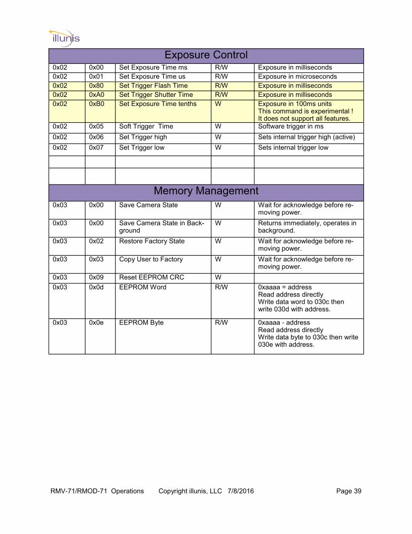
Exposure Control 0x02 0x00 Set Exposure Time ms R/W Exposure in milliseconds
0x02 0x01 Set Exposure Time us R/W Exposure in microseconds
0x02 0x80 Set Trigger Flash Time R/W Exposure in milliseconds
0x02 0xA0 Set Trigger Shutter Time R/W Exposure in milliseconds
0x02 0xB0 Set Exposure Time tenths W Exposure in 100ms units This command is experimental ! It does not support all features.
0x02 0x05 Soft Trigger Time W Software trigger in ms
0x02 0x06 Set Trigger high W Sets internal trigger high (active)
0x02 0x07 Set Trigger low W Sets internal trigger low
Memory Management
0x03 0x00 Save Camera State W Wait for acknowledge before re-moving power.
0x03 0x00 Save Camera State in Back-ground
W Returns immediately, operates in background.
0x03 0x02 Restore Factory State W Wait for acknowledge before re-moving power.
0x03 0x03 Copy User to Factory W Wait for acknowledge before re-moving power.
0x03 0x09 Reset EEPROM CRC W
0x03 0x0d EEPROM Word R/W 0xaaaa = address Read address directly Write data word to 030c then write 030d with address.
0x03 0x0e EEPROM Byte R/W 0xaaaa - address Read address directly Write data byte to 030c then write 030e with address.
RMV-71/RMOD-71 Operations Copyright illunis, LLC 7/8/2016 Page 40
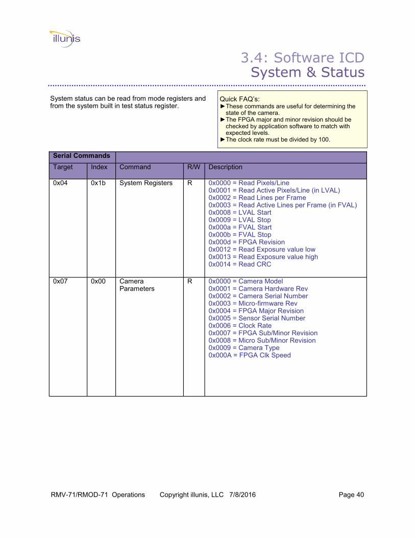
System status can be read from mode registers and from the system built in test status register.
Serial Commands
Target Index Command R/W Description
0x04 0x1b System Registers R 0x0000 = Read Pixels/Line 0x0001 = Read Active Pixels/Line (in LVAL) 0x0002 = Read Lines per Frame 0x0003 = Read Active Lines per Frame (in FVAL) 0x0008 = LVAL Start 0x0009 = LVAL Stop 0x000a = FVAL Start 0x000b = FVAL Stop 0x000d = FPGA Revision 0x0012 = Read Exposure value low 0x0013 = Read Exposure value high 0x0014 = Read CRC
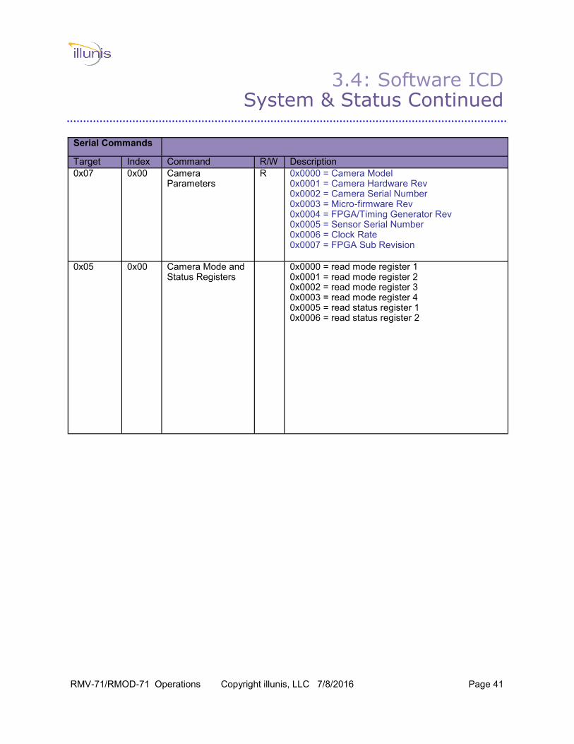
0x07 0x00 Camera Parameters
R 0x0000 = Camera Model 0x0001 = Camera Hardware Rev 0x0002 = Camera Serial Number 0x0003 = Micro-firmware Rev 0x0004 = FPGA Major Revision 0x0005 = Sensor Serial Number 0x0006 = Clock Rate 0x0007 = FPGA Sub/Minor Revision 0x0008 = Micro Sub/Minor Revision 0x0009 = Camera Type 0x000A = FPGA Clk Speed
Quick FAQ’s: ►These commands are useful for determining the
state of the camera. ►The FPGA major and minor revision should be
checked by application software to match with expected levels.
►The clock rate must be divided by 100.
3.4: Software ICD System & Status
RMV-71/RMOD-71 Operations Copyright illunis, LLC 7/8/2016 Page 41
Serial Commands
Target Index Command R/W Description
0x07 0x00 Camera Parameters
R 0x0000 = Camera Model 0x0001 = Camera Hardware Rev 0x0002 = Camera Serial Number 0x0003 = Micro-firmware Rev 0x0004 = FPGA/Timing Generator Rev 0x0005 = Sensor Serial Number 0x0006 = Clock Rate 0x0007 = FPGA Sub Revision
0x05 0x00 Camera Mode and Status Registers
0x0000 = read mode register 1 0x0001 = read mode register 2 0x0002 = read mode register 3 0x0003 = read mode register 4 0x0005 = read status register 1 0x0006 = read status register 2
3.4: Software ICD System & Status Continued
RMV-71/RMOD-71 Operations Copyright illunis, LLC 7/8/2016 Page 42
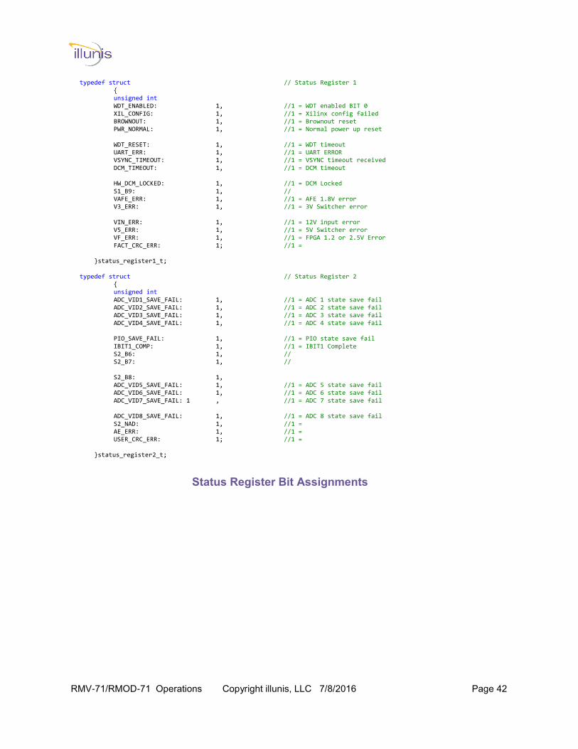
Status Register Bit Assignments
typedef struct // Status Register 1 { unsigned int WDT_ENABLED: 1, //1 = WDT enabled BIT 0 XIL_CONFIG: 1, //1 = Xilinx config failed BROWNOUT: 1, //1 = Brownout reset PWR_NORMAL: 1, //1 = Normal power up reset WDT_RESET: 1, //1 = WDT timeout UART_ERR: 1, //1 = UART ERROR VSYNC_TIMEOUT: 1, //1 = VSYNC timeout received DCM_TIMEOUT: 1, //1 = DCM timeout HW_DCM_LOCKED: 1, //1 = DCM Locked S1_B9: 1, // VAFE_ERR: 1, //1 = AFE 1.8V error V3_ERR: 1, //1 = 3V Switcher error VIN_ERR: 1, //1 = 12V input error V5_ERR: 1, //1 = 5V Switcher error VF_ERR: 1, //1 = FPGA 1.2 or 2.5V Error FACT_CRC_ERR: 1; //1 = }status_register1_t; typedef struct // Status Register 2 { unsigned int ADC_VID1_SAVE_FAIL: 1, //1 = ADC 1 state save fail ADC_VID2_SAVE_FAIL: 1, //1 = ADC 2 state save fail ADC_VID3_SAVE_FAIL: 1, //1 = ADC 3 state save fail ADC_VID4_SAVE_FAIL: 1, //1 = ADC 4 state save fail PIO_SAVE_FAIL: 1, //1 = PIO state save fail IBIT1_COMP: 1, //1 = IBIT1 Complete S2_B6: 1, // S2_B7: 1, // S2_B8: 1, ADC_VID5_SAVE_FAIL: 1, //1 = ADC 5 state save fail ADC_VID6_SAVE_FAIL: 1, //1 = ADC 6 state save fail ADC_VID7_SAVE_FAIL: 1 , //1 = ADC 7 state save fail ADC_VID8_SAVE_FAIL: 1, //1 = ADC 8 state save fail S2_NAD: 1, //1 = AE_ERR: 1, //1 = USER_CRC_ERR: 1; //1 = }status_register2_t;

RMV-71/RMOD-71 Operations Copyright illunis, LLC 7/8/2016 Page 43
Mode Register Bit Assignments
typedef struct // Mode Register 1 = READOUT { unsigned int free_run: 1, // 1 = free run mode 0 = trigger strobe_polarity: 1, // 1 = positive strobe polarity trigger_polarity: 1, // 1 = positive trigger polarity trigger_source: 1, // 0 = CL 1 = External twelve_bit: 1, // 1 = 12 bit readout ten_bit: 1, // 1 = 10 bit readout eight_bit: 1, // 1 = 8 bit readout bottom_8: 1, // 1 = bottom 8 bit readout input_TP: 1, // 1 = input test pattern enabled output_TP: 1, // 1 = output test pattern enabled Med_mode_readout: 1, //1 = Medium mode readout (4 tap path) Base_mode_readout: 1, //1 = Base mode readout (2 tap path) full_readout: 1, // 1 = 10,000 x 7096 0 = window osc_42mhz: 1, Osc_30mhz: 1, Osc_div2: 1; } mode_register1_t; typedef struct // Mode Register 2 = Defect and image correction { unsigned int DGO_enabled: 1, // Master Digital gain and offset LUT_enabled: 1, LUT_LOADED: 1, //1 = LUT Loaded from EEPROM HISTO_EQ: 1, //1 = Histogram equalization enabled CDC_EN: 1, //1 = Column Defect Corrector Enabled PDC_EN: 1, //1 = Pixel Defect Corrector Enabled RDC_EN: 1, //1 = Row Defect Corrector Enabled M2_B7: 1, // CGT_enabled: 1, CGT_LOADED: 1, //1 = Column Gain Table Loaded from EEPROM COT_enabled: 1, COT_LOADED: 1, //1 = Column Offset Table Loaded from EEPROM M2_BC: 1, // M2_BD: 1, // M2_BE: 1, // M2_BF: 1; // } mode_register2_t; typedef struct // Mode Register 3 = Detectors and AE { unsigned int AE: 1, //1 = auto exposure enabled AE_gain: 1, //1 = AE_exposure: 1, //1 = AE in exposure mode AE_iris: 1, //1 = AE_hysteresis: 1, //1 = AE within hysteresis AE_OPEN_IRIS: 1, //1 = AE at max gain - need more light BIT 0 PRESERVE AE_CLOSE_IRIS: 1, //1 = AE at min exposure - need less light PRESERVE OSD_CP: 1, // OSD_TEXT: 1, //1 = OSD text display enabled PRESERVE OSD_2X: 1, //1 = 2X text box BIT0 OSD_COLOR_MODE: 1, //1 = OSD Color Mode OSD_LP: 1, // OSD_SCR: 4; //1 = OSD Screen type ( bits) } mode_register3_t; typedef struct // Mode Register 4 = Communication and misc. { unsigned int AE_WINDOW: 1, //1 = Show AE Window AF_WINDOW: 1, //1 = Show AF Window AF_DATA: 1, //1 = Show AF Data AF_FULL: 1, //1 = Show AF Data Full Screen BAUD_9600: 1, //1 = 9600 baud BAUD_19200: 1, //1 = 19200 baud BAUD_38400: 1, //1 = 38400 baud BAUD_57600: 1, //1 = 57600 baud BAUD_115200: 1, //1 = 115200 baud HotPixelEnabled 1, // HotPixelMono 1, // M4_BB: 1, // TriggeredFlash: 1, // TriggeredShutter: 1, // CLK_SEL: 1, // PowerDown: 1; // } mode_register4_t;
RMV-71/RMOD-71 Operations Copyright illunis, LLC 7/8/2016 Page 44
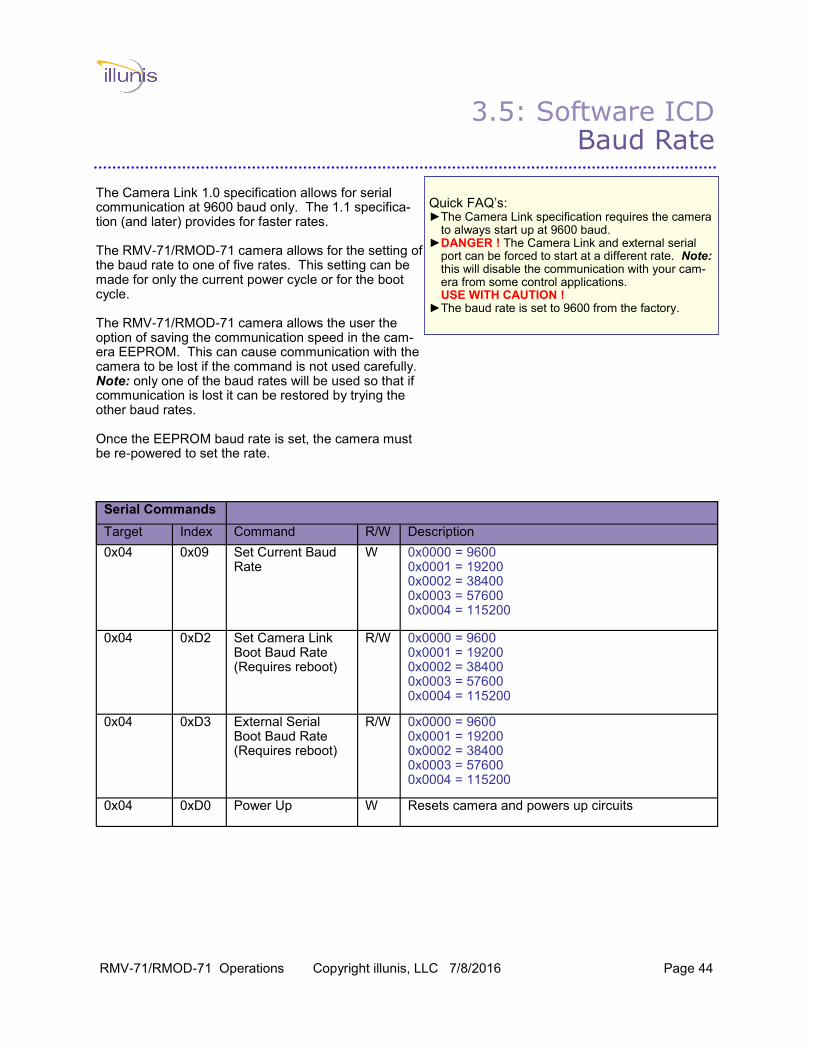
The Camera Link 1.0 specification allows for serial communication at 9600 baud only. The 1.1 specifica-tion (and later) provides for faster rates. The RMV-71/RMOD-71 camera allows for the setting of the baud rate to one of five rates. This setting can be made for only the current power cycle or for the boot cycle. The RMV-71/RMOD-71 camera allows the user the option of saving the communication speed in the cam-era EEPROM. This can cause communication with the camera to be lost if the command is not used carefully. Note: only one of the baud rates will be used so that if communication is lost it can be restored by trying the other baud rates. Once the EEPROM baud rate is set, the camera must be re-powered to set the rate.
Serial Commands
Target Index Command R/W Description
0x04 0x09 Set Current Baud Rate
W 0x0000 = 9600 0x0001 = 19200 0x0002 = 38400 0x0003 = 57600 0x0004 = 115200
0x04 0xD2 Set Camera Link Boot Baud Rate (Requires reboot)
R/W 0x0000 = 9600 0x0001 = 19200 0x0002 = 38400 0x0003 = 57600 0x0004 = 115200
0x04 0xD3 External Serial Boot Baud Rate (Requires reboot)
R/W 0x0000 = 9600 0x0001 = 19200 0x0002 = 38400 0x0003 = 57600 0x0004 = 115200
0x04 0xD0 Power Up W Resets camera and powers up circuits
Quick FAQ’s: ►The Camera Link specification requires the camera
to always start up at 9600 baud. ►DANGER ! The Camera Link and external serial
port can be forced to start at a different rate. Note: this will disable the communication with your cam-era from some control applications.
USE WITH CAUTION ! ►The baud rate is set to 9600 from the factory.
3.5: Software ICD Baud Rate
RMV-71/RMOD-71 Operations Copyright illunis, LLC 7/8/2016 Page 45
3.6: Graphical User Interface (GUI) Overview and Installation
Overview The RMV-71/RMOD-71 camera is feature rich and may be complicated to interface. To ease the intro-duction to the RMV-71/RMOD-71 command set and to allow easy user control of the camera, illunis has provided a graphical user interface (GUI). The GUI is a visual program that consists of several windows, menus, and dialog boxes for each of the many features of the RMV-71/RMOD-71 camera. The GUI is installed using a standard windows installer program available from the illunis website. For GUI software, please visit the illunis website at: http://illunis.com. Use the NEW .net version for the RMV-71/RMOD-71 .
Software: Camera Link based software: Camera control is accomplished through a Visual Basic application, which controls all camera functions using the capture card supplied communication.dll. See http://illunis.com for 32 and 64 bit control application installers.
Gigabit Ethernet based software: Our GigE based cameras use the Pleora Interface and software for transmitting video and related con-trol data over standard Ethernet platforms. Pleora software is a third party, and illunis, LLC is not responsible for the contents of their manual, soft-ware, and website. Below is the direct link to the Pleora website. http://www.pleora.com/our-products/embedded-hardware/iport-ntx-mini
USB3 based software: Please contact illunis at [email protected] or call (952) 975-9203.
RMV-71/RMOD-71 Operations Copyright illunis, LLC 7/8/2016 Page 46
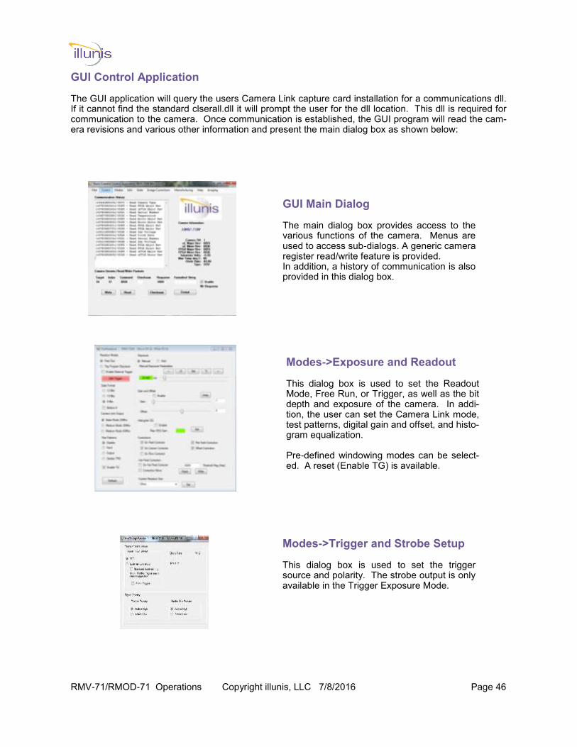
GUI Control Application The GUI application will query the users Camera Link capture card installation for a communications dll. If it cannot find the standard clserall.dll it will prompt the user for the dll location. This dll is required for communication to the camera. Once communication is established, the GUI program will read the cam-era revisions and various other information and present the main dialog box as shown below:
GUI Main Dialog The main dialog box provides access to the various functions of the camera. Menus are used to access sub-dialogs. A generic camera register read/write feature is provided. In addition, a history of communication is also provided in this dialog box.
Modes->Exposure and Readout This dialog box is used to set the Readout Mode, Free Run, or Trigger, as well as the bit depth and exposure of the camera. In addi-tion, the user can set the Camera Link mode, test patterns, digital gain and offset, and histo-gram equalization. Pre-defined windowing modes can be select-ed. A reset (Enable TG) is available.
Modes->Trigger and Strobe Setup This dialog box is used to set the trigger source and polarity. The strobe output is only available in the Trigger Exposure Mode.
RMV-71/RMOD-71 Operations Copyright illunis, LLC 7/8/2016 Page 47
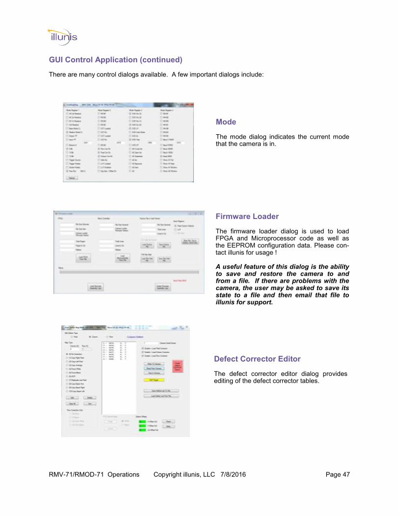
Mode The mode dialog indicates the current mode that the camera is in.
GUI Control Application (continued) There are many control dialogs available. A few important dialogs include:
Firmware Loader The firmware loader dialog is used to load FPGA and Microprocessor code as well as the EEPROM configuration data. Please con-tact illunis for usage ! A useful feature of this dialog is the ability to save and restore the camera to and from a file. If there are problems with the camera, the user may be asked to save its state to a file and then email that file to illunis for support.
Defect Corrector Editor The defect corrector editor dialog provides editing of the defect corrector tables.
RMV-71/RMOD-71 Operations Copyright illunis, LLC 7/8/2016 Page 48
3.7: Graphical User Interface (GUI) Camera Update/Backup
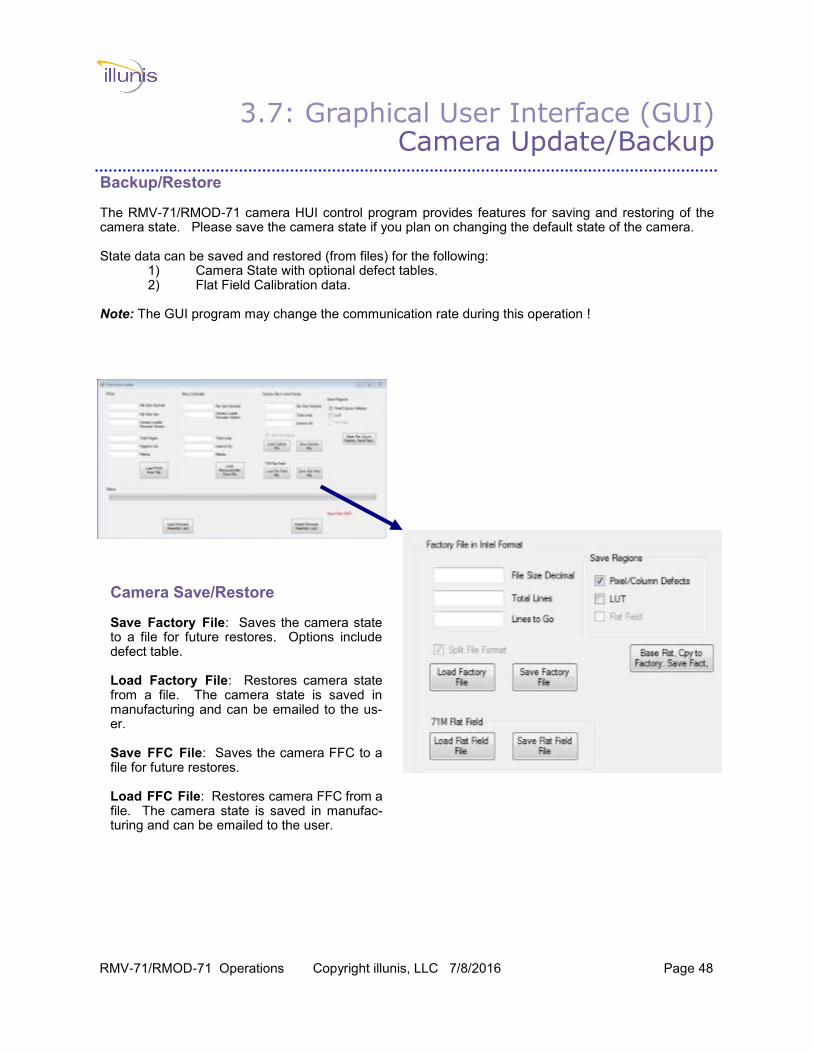
Backup/Restore The RMV-71/RMOD-71 camera HUI control program provides features for saving and restoring of the camera state. Please save the camera state if you plan on changing the default state of the camera. State data can be saved and restored (from files) for the following: 1) Camera State with optional defect tables. 2) Flat Field Calibration data. Note: The GUI program may change the communication rate during this operation !
Camera Save/Restore Save Factory File: Saves the camera state to a file for future restores. Options include defect table. Load Factory File: Restores camera state from a file. The camera state is saved in manufacturing and can be emailed to the us-er. Save FFC File: Saves the camera FFC to a file for future restores. Load FFC File: Restores camera FFC from a file. The camera state is saved in manufac-turing and can be emailed to the user.

RMV-71/RMOD-71 Operations Copyright illunis, LLC 7/8/2016 Page 49
Firmware Loader Load FPGA from file: Loads the FPGA con-figuration data, the camera must be repow-ered to enable the new configuration. Load Microcontroller from file: Loads the Micro configuration data, the camera must be repowered to enable the new configuration.
3.7: Graphical User Interface (GUI) Cont. Camera Firmware Update
Backup/Restore The RMV-71/RMOD-71 camera HUI control program provides features for saving and restoring the cam-era firmware. Firmware can be loaded (from files) for the following: 1) FPGA configuration. 2) Microprocessor configuration. Note: The GUI program may change the communication rate during this operation !
Warning: Do not remove power during an update ! This will disable the camera
and the camera will have to be returned for repair.
RMV-71/RMOD-71 Operations Copyright illunis, LLC 7/8/2016 Page 50
Chapte
r 4:
Image E
xposure
Ru
gg
ed
Mach
ine V
isio
n
4.0 Image Exposure Overview 4.1.1 Set Exposure Type 4.1.2 Set Exposure Time
4.2 Window Readout 4.3 Strobe Signal 4.4 Software Controlled Trigger 4.5 Gain & Black Level 4.6 Triggered Strobe, Flash, and Shutter Operation
RMV-71/RMOD-71 Operations Copyright illunis, LLC 7/8/2016 Page 51
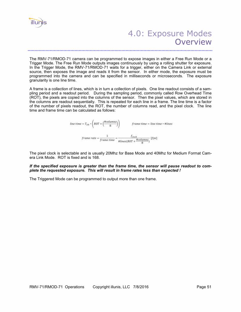
4.0: Exposure Modes Overview
The RMV-71/RMOD-71 camera can be programmed to expose images in either a Free Run Mode or a Trigger Mode. The Free Run Mode outputs images continuously by using a rolling shutter for exposure. In the Trigger Mode, the RMV-71/RMOD-71 waits for a trigger, either on the Camera Link or external source, then exposes the image and reads it from the sensor. In either mode, the exposure must be programmed into the camera and can be specified in milliseconds or microseconds. The exposure granularity is one line time. A frame is a collection of lines, which is in turn a collection of pixels. One line readout consists of a sam-pling period and a readout period. During the sampling period, commonly called Row Overhead Time (ROT), the pixels are copied into the columns of the sensor. Then the pixel values, which are stored in the columns are readout sequentially. This is repeated for each line in a frame. The line time is a factor of the number of pixels readout, the ROT, the number of columns read, and the pixel clock. The line time and frame time can be calculated as follows: The pixel clock is selectable and is usually 20Mhz for Base Mode and 40Mhz for Medium Format Cam-era Link Mode. ROT is fixed and is 168. If the specified exposure is greater than the frame time, the sensor will pause readout to com-plete the requested exposure. This will result in frame rates less than expected ! The Triggered Mode can be programmed to output more than one frame.
RMV-71/RMOD-71 Operations Copyright illunis, LLC 7/8/2016 Page 52
4.1.1: Exposure: Set Exposure Type
The exposure type is either Free Run Mode or Trigger Mode. In Free Run Mode, the camera outputs continuous images in a rolling shutter mode. In Trigger Mode, the camera receives the trigger, eras-es the pixels, exposes the image, and then reads it out.
Serial Commands
Target Index Command R/W Description
0x04 0x03 0x0000 W Set Free Run Mode
0x04 0x03 0x0001 W Set Trigger Mode
0x02 0x80 Set Trigger Flash Time R/W Exposure in milliseconds
0x02 0xA0 Set Trigger Shutter Time
R/W Exposure in milliseconds
0x5C 0x01 # of frames W Set number frames read in Trigger Mode
0x04 0x03 0x0009 W Set Trigger Source Camera Link
0x04 0x03 0x000A W Set Trigger Source power cable (external)
Quick FAQ’s: ►Exposure time must be set for each mode.
4.1.2: Exposure: Free Run Mode Set Exposure Time
The exposure time is set in either milliseconds or mi-croseconds. The resolution of the exposure is in hori-zontal line times. Two commands are provided for calculating the Free Run time from a specified time variable (milliseconds or microseconds). The closest available time is selected and set in the internal time variable.
Serial Commands
Target Index Command R/W Description
0x02 0x02 Set Exposure ms W Set Exposure time in milliseconds
0x02 0x03 Set Exposure us W Set Exposure time in us
0x02 0x02 Get Exposure ms R Return actual time in milliseconds
0x02 0x03 Get Exposure us R Return actual time in us (0xFFFF = to large).
Quick FAQ’s: ►The strobe signal can be found on the RMV-71/
RMOD-71 power connector and is a 3.3V LVTTL signal. Note: The strobe is functional only in the Trigger Mode.
RMV-71/RMOD-71 Operations Copyright illunis, LLC 7/8/2016 Page 53
4.2: Exposure: Windowed Readout
The Windowed Readout command changes the raster readout of the CHR71M sensor. Window sizes are rounded to 16 pixels horizontally and 8 pixels vertically.
Serial Commands
Target Index Command R/W Description
0x5C 0x10 Window Y Start R/W Location in pixels, will be rounded to nearest 8th row.
0x5C 0x11 Window X Start R/W Location in pixels, will be rounded to nearest 16th column.
0x5C 0x12 Window Y Stop R/W Location in pixels, will be rounded to nearest 8th row.
0x5C 0x13 Window X Stop R/W Location in pixels, will be rounded to nearest 16th column.
0x5E 0x00 Full Readout W Sensor 10,000x7096 output
0x5E 0x01 Pre-set Window W Window 1920x1080 in center of sensor
0x5E 0x02 Pre-set Window W Window 3830x2160 in center of sensor
0x5E 0x03 Pre-set Window W Window 640x480 in center of sensor
0x5E 0x04 Pre-set Window W Window 7680x4320 in center of sensor
0x5E 0x05 Pre-set Window W Window 256x256 in center of sensor
0x5E 0x06 Pre-set Window W Window 1024x1024 in center of sensor
0x5E 0x07 Pre-set Window W Window 2048x2048 in center of sensor
0x5E 0x08 Pre-set Window W Window 4096x4096 in center of sensor
0x5E 0x09 Pre-set Window W Window 7096x7096 in center of sensor
0x5E 0x0A Pre-set Window W Window 10000x1080 in center of sensor
0x5E 0x80 Set Window Readout W Must setup X/Y size as below
0x5E 0x81 Set Window X size W Sets width of centered window
0x5E 0x82 Set Window Y size W Sets height of centered window
0x5E 0xD0 Get Line Time R Returns line time in us
0x5E 0xD1 Get Frame Time R Returns frame time in us
0x5E 0xD2 Get Frame Time R Returns frame time in ms
Quick FAQ’s: ►Windowing will increase the frame rate. Use the
equations in the beginning of this chapter to calculate line and frame times (see page 51).
RMV-71/RMOD-71 Operations Copyright illunis, LLC 7/8/2016 Page 54
4.4: Exposure: Software Controlled Trigger
The Software Controlled Trigger command forces an internal trigger from a software command. The soft trigger pulse has a width in us as specified in the data field. The range is 1 to 65535 ms (65sec) where 10ms is typical usage.
Serial Commands
Target Index Command R/W Description
0x02 0x05 Soft Trigger W Issue a Soft Trigger with width in ms
0x02 0x06 Soft Trigger high W Sets Trigger high
0x02 0x07 Soft Trigger low W Sets Trigger low
Quick FAQ’s: ►Exposure must be programmed before issuing any
trigger !
►Hardware triggers must be inactive when using Software Trigger !
4.3: Exposure: Strobe Signal
The RMV-71/RMOD-71 Strobe Signal is a 3.3V LVTTL signal that is active when the sensor is triggered and exposing an image. The Strobe Signal is useful for analyzing and optimizing imaging applications. The strobe can be used to activate an illumination source. If used in this fashion, the Strobe Signal cannot drive signif-icant current and should be buffered.
Quick FAQ’s: ►The Strobe Signal can be used to determine
Triggered Frame Timing.
►The Strobe Signal can be found on the RMV-71/RMOD-71 power connector and is a 3.3V LVTTL signal.
Serial Commands
Target Index Command R/W Description
0x04 0x0e Strobe Control
Write 0x0000 = negative strobe polarity 0x0001 = positive strobe polarity
RMV-71/RMOD-71 Operations Copyright illunis, LLC 7/8/2016 Page 55
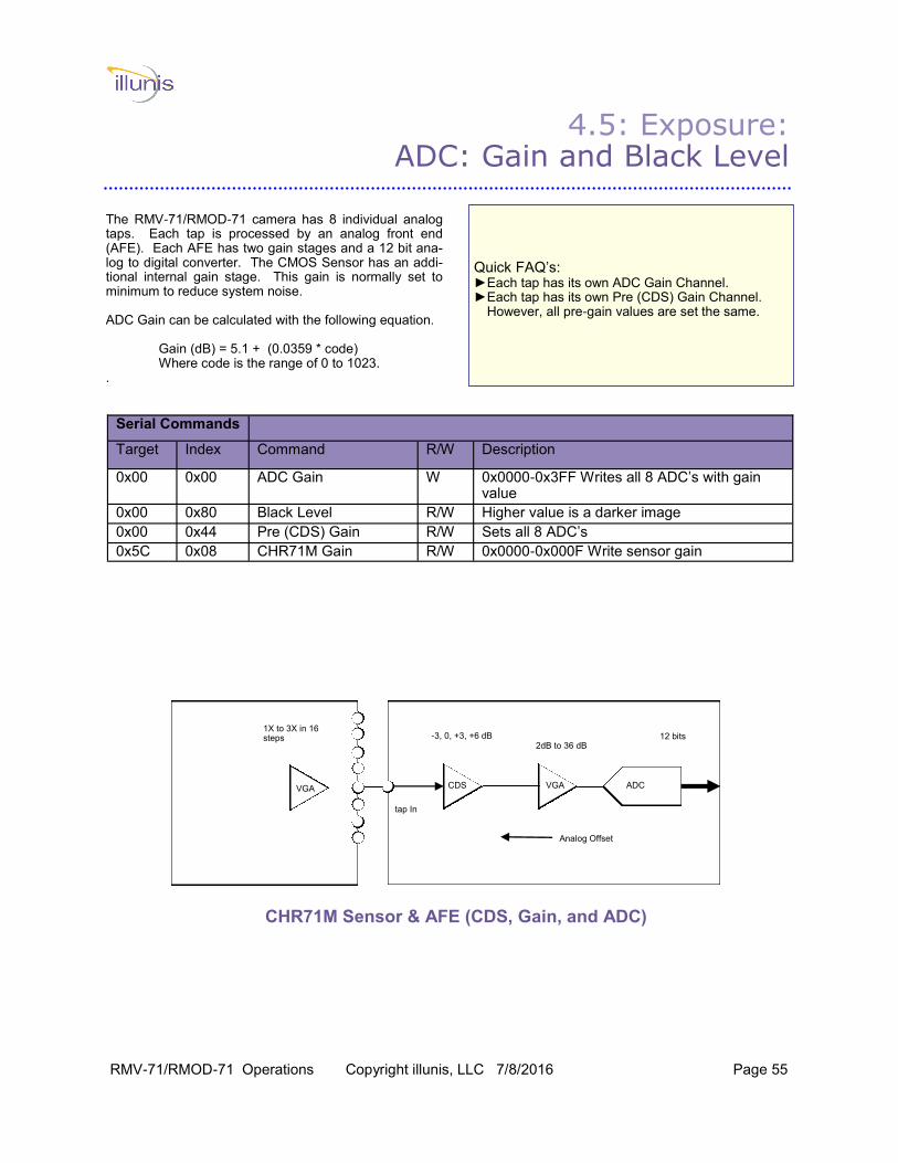
4.5: Exposure: ADC: Gain and Black Level
Serial Commands
Target Index Command R/W Description
0x00 0x00 ADC Gain W 0x0000-0x3FF Writes all 8 ADC’s with gain value
0x00 0x80 Black Level R/W Higher value is a darker image
0x00 0x44 Pre (CDS) Gain R/W Sets all 8 ADC’s
0x5C 0x08 CHR71M Gain R/W 0x0000-0x000F Write sensor gain
The RMV-71/RMOD-71 camera has 8 individual analog taps. Each tap is processed by an analog front end (AFE). Each AFE has two gain stages and a 12 bit ana-log to digital converter. The CMOS Sensor has an addi-tional internal gain stage. This gain is normally set to minimum to reduce system noise. ADC Gain can be calculated with the following equation.
Gain (dB) = 5.1 + (0.0359 * code) Where code is the range of 0 to 1023.
.
Quick FAQ’s: ►Each tap has its own ADC Gain Channel. ►Each tap has its own Pre (CDS) Gain Channel.
However, all pre-gain values are set the same.
CHR71M Sensor & AFE (CDS, Gain, and ADC)
CDS VGA ADC
2dB to 36 dB 12 bits
tap In
-3, 0, +3, +6 dB
VGA
1X to 3X in 16 steps
Analog Offset
RMV-71/RMOD-71 Operations Copyright illunis, LLC 7/8/2016 Page 56
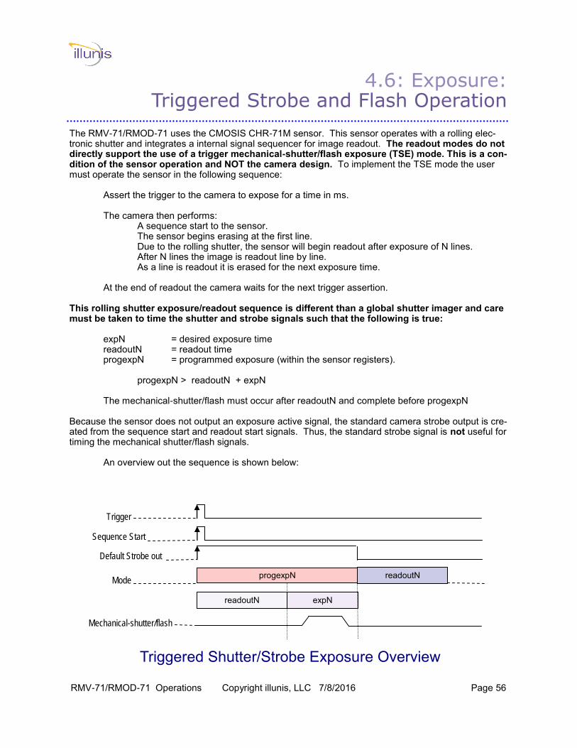
4.6: Exposure: Triggered Strobe and Flash Operation
Triggered Shutter/Strobe Exposure Overview
progexpN readoutN
Trigger
Mode
Mechanical-shutter/flash
Sequence Start
readoutN expN
Default Strobe out
The RMV-71/RMOD-71 uses the CMOSIS CHR-71M sensor. This sensor operates with a rolling elec-tronic shutter and integrates a internal signal sequencer for image readout. The readout modes do not directly support the use of a trigger mechanical-shutter/flash exposure (TSE) mode. This is a con-dition of the sensor operation and NOT the camera design. To implement the TSE mode the user must operate the sensor in the following sequence: Assert the trigger to the camera to expose for a time in ms. The camera then performs: A sequence start to the sensor. The sensor begins erasing at the first line. Due to the rolling shutter, the sensor will begin readout after exposure of N lines. After N lines the image is readout line by line. As a line is readout it is erased for the next exposure time. At the end of readout the camera waits for the next trigger assertion. This rolling shutter exposure/readout sequence is different than a global shutter imager and care must be taken to time the shutter and strobe signals such that the following is true: expN = desired exposure time readoutN = readout time progexpN = programmed exposure (within the sensor registers). progexpN > readoutN + expN The mechanical-shutter/flash must occur after readoutN and complete before progexpN Because the sensor does not output an exposure active signal, the standard camera strobe output is cre-ated from the sequence start and readout start signals. Thus, the standard strobe signal is not useful for timing the mechanical shutter/flash signals. An overview out the sequence is shown below:
RMV-71/RMOD-71 Operations Copyright illunis, LLC 7/8/2016 Page 57
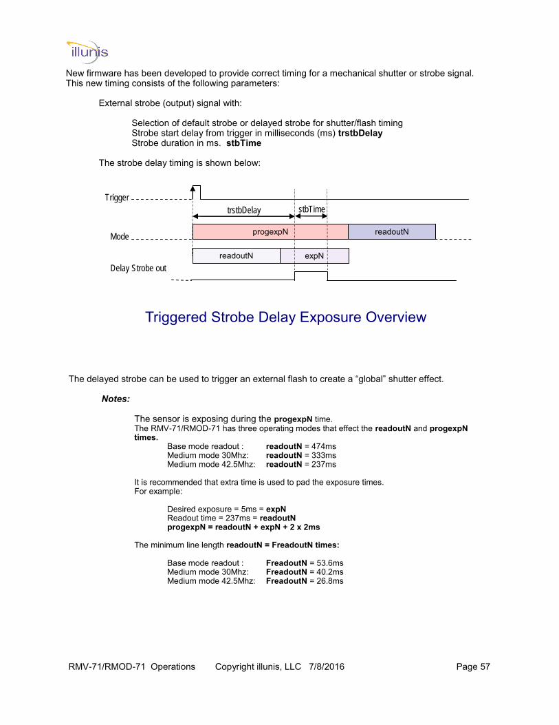
New firmware has been developed to provide correct timing for a mechanical shutter or strobe signal. This new timing consists of the following parameters: External strobe (output) signal with: Selection of default strobe or delayed strobe for shutter/flash timing Strobe start delay from trigger in milliseconds (ms) trstbDelay Strobe duration in ms. stbTime The strobe delay timing is shown below:
Triggered Strobe Delay Exposure Overview
progexpN readoutN
Trigger
Mode
readoutN expN
Delay Strobe out
trstbDelay stbTime
The delayed strobe can be used to trigger an external flash to create a “global” shutter effect. Notes: The sensor is exposing during the progexpN time. The RMV-71/RMOD-71 has three operating modes that effect the readoutN and progexpN times. Base mode readout : readoutN = 474ms Medium mode 30Mhz: readoutN = 333ms Medium mode 42.5Mhz: readoutN = 237ms It is recommended that extra time is used to pad the exposure times. For example: Desired exposure = 5ms = expN Readout time = 237ms = readoutN progexpN = readoutN + expN + 2 x 2ms The minimum line length readoutN = FreadoutN times: Base mode readout : FreadoutN = 53.6ms Medium mode 30Mhz: FreadoutN = 40.2ms Medium mode 42.5Mhz: FreadoutN = 26.8ms
RMV-71/RMOD-71 Operations Copyright illunis, LLC 7/8/2016 Page 58
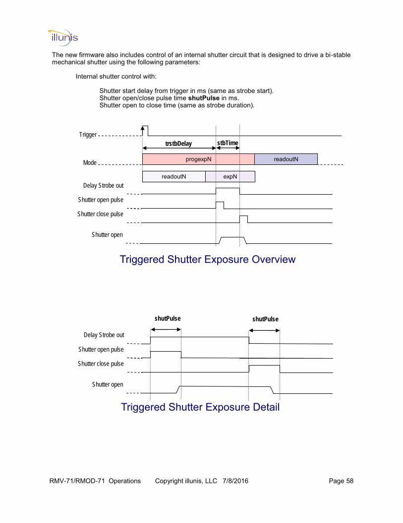
The new firmware also includes control of an internal shutter circuit that is designed to drive a bi-stable mechanical shutter using the following parameters: Internal shutter control with: Shutter start delay from trigger in ms (same as strobe start). Shutter open/close pulse time shutPulse in ms. Shutter open to close time (same as strobe duration).
Triggered Shutter Exposure Overview
progexpN readoutN
Trigger
Mode
readoutN expN
Delay Strobe out
trstbDelay stbTime
Shutter open pulse
Shutter close pulse
Shutter open
Shutter open pulse
Shutter close pulse
Shutter open
Triggered Shutter Exposure Detail
Delay Strobe out
shutPulse shutPulse

RMV-71/RMOD-71 Operations Copyright illunis, LLC 7/8/2016 Page 59
4.6: Exposure: Triggered Strobe and Flash Operation Cont...
These functions set the parameters associated with the triggered shutter/flash strobe output. Note: These are specialized commands and must be sent to the camera individually from the GUI control software. Opening the GUI exposure and readout dialog will reset these commands ! Use the “SetTriggeredFlash” command for setup. {0280xxxxCS}
Serial Commands
Target Index Command R/W Description
0x02 0x10 0x0000 W Set Standard Strobe Mode
0x02 0x10 0x0001 W Set Delay Strobe Mode
0x02 0x11 ms R/W Set Strobe Delay in ms
0x02 0x12 ms R/W Set Strobe Duration in ms
0x02 0x13 0x0001 R/W Set Shutter Active
0x02 0x13 0x0000 R/W Set Shutter Inactive
0x02 0x14 ms R/W Set Shutter Pulse Width in ms
0x02 0x15 0x0000 0x0001
R/W Set Shutter Open-Close sequence (Open-Close or Close-Open)
0x02 0x16 0x765F 30303 dec
R/W ms_tick divider
Quick FAQ’s: ►Refer to the app. note for details on these modes.
►Timing is depent on the readout mode: Base mode: 474ms readout time Med. 30Mhz: 333ms readout time Med. 42.5Mhz: 237ms readout time Example: Base mode, Flash, 30ms exposure Standard strobe mode Strobe delay = 496ms = readout * 1.05 Strobe duration = 30ms Triggered exposure = 496 + 30 + 2 = 528ms
Serial Commands
Target Index Command R/W Description
0x02 0x80 Flash pulse in ms W Set Trigged Flash Exposure in ms
This function will set the trigger timing for flash use based on the readout time and desired flash time.
Quick FAQ’s: ►All times are in ms. Due to the long delays of this
timing mode only ms are supported.
►Small Flash times may not pass correctly. Use times of 5ms or more for driving relays.
►The strobe output of the RMV-71/RMOD-71 camera is a LVTTL that can drive a 5V relay which can trigger a flash pack.
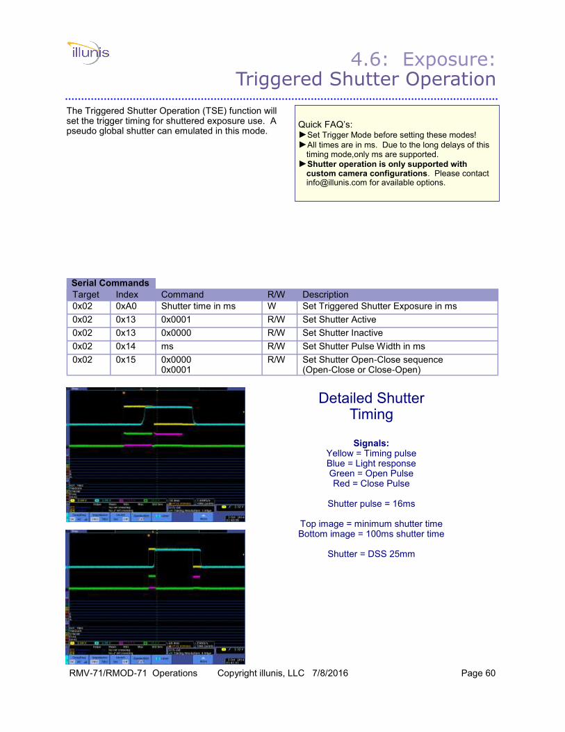
RMV-71/RMOD-71 Operations Copyright illunis, LLC 7/8/2016 Page 60
Detailed Shutter Timing
Signals:
Yellow = Timing pulse Blue = Light response Green = Open Pulse Red = Close Pulse
Shutter pulse = 16ms
Top image = minimum shutter time Bottom image = 100ms shutter time
Shutter = DSS 25mm
4.6: Exposure: Triggered Shutter Operation
The Triggered Shutter Operation (TSE) function will set the trigger timing for shuttered exposure use. A pseudo global shutter can emulated in this mode.
Serial Commands
Target Index Command R/W Description
0x02 0xA0 Shutter time in ms W Set Triggered Shutter Exposure in ms
0x02 0x13 0x0001 R/W Set Shutter Active
0x02 0x13 0x0000 R/W Set Shutter Inactive
0x02 0x14 ms R/W Set Shutter Pulse Width in ms
0x02 0x15 0x0000 0x0001
R/W Set Shutter Open-Close sequence (Open-Close or Close-Open)
Quick FAQ’s: ►Set Trigger Mode before setting these modes! ►All times are in ms. Due to the long delays of this
timing mode,only ms are supported.
►Shutter operation is only supported with custom camera configurations. Please contact [email protected] for available options.

RMV-71/RMOD-71 Operations Copyright illunis, LLC 7/8/2016 Page 61
3-5V ‘NO’ Reed
Relay
Flash
RMV-71/RMOD-71
Triggered Flash Test Circuit Test circuit used common radio shack Relay Model 275-232
Strobe Signal
Trigger Signal
RMV-71/RMOD-71 Operations Copyright illunis, LLC 7/8/2016 Page 62
Chapte
r 5:
Image P
rocessin
g
R
ug
ged
Mach
ine V
isio
n 5.0 Overview
5.1 Tap Output Order 5.2 Digital Gain & Offset 5.3 Defect Correction 5.4 Flat Field Correction 5.5 Offset Calibration 5.6 Histogram Equalization 5.7 Hot Pixel Correction 5.8 Very Long Exposures
RMV-71/RMOD-71 Operations Copyright illunis, LLC 7/8/2016 Page 63
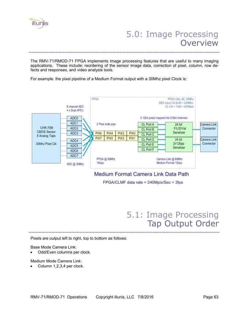
5.0: Image Processing Overview
The RMV-71/RMOD-71 FPGA implements image processing features that are useful to many imaging applications. These include: reordering of the sensor image data, correction of pixel, column, row de-fects and responses, and video analysis tools. For example. the pixel pipeline of a Medium Format output with a 30Mhz pixel Clock is:
5.1: Image Processing Tap Output Order
Pixels are output left to right, top to bottom as follows: Base Mode Camera Link:
Odd/Even columns per clock. Medium Mode Camera Link:
Column 1,2,3,4 per clock.
RMV-71/RMOD-71 Operations Copyright illunis, LLC 7/8/2016 Page 64
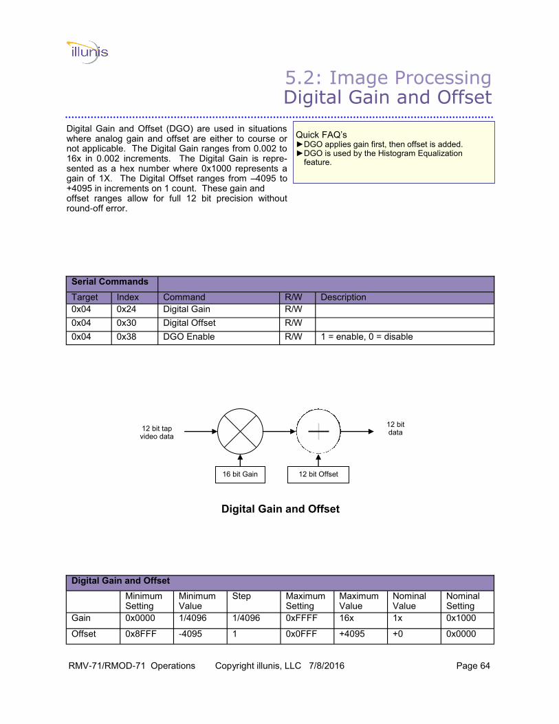
5.2: Image Processing Digital Gain and Offset
Digital Gain and Offset (DGO) are used in situations where analog gain and offset are either to course or not applicable. The Digital Gain ranges from 0.002 to 16x in 0.002 increments. The Digital Gain is repre-sented as a hex number where 0x1000 represents a gain of 1X. The Digital Offset ranges from –4095 to +4095 in increments on 1 count. These gain and offset ranges allow for full 12 bit precision without round-off error.
Serial Commands
Target Index Command R/W Description
0x04 0x24 Digital Gain R/W
0x04 0x30 Digital Offset R/W
0x04 0x38 DGO Enable R/W 1 = enable, 0 = disable
Quick FAQ’s ►DGO applies gain first, then offset is added. ►DGO is used by the Histogram Equalization
feature.
Digital Gain and Offset
Minimum Setting
Minimum Value
Step Maximum Value
Nominal Value
Nominal Setting
Maximum Setting
Gain 0x0000 1/4096 1/4096 16x 1x 0x1000 0xFFFF
Offset 0x8FFF -4095 1 +4095 +0 0x0000 0x0FFF
Digital Gain and Offset
16 bit Gain 12 bit Offset
12 bit data
12 bit tap video data
RMV-71/RMOD-71 Operations Copyright illunis, LLC 7/8/2016 Page 65
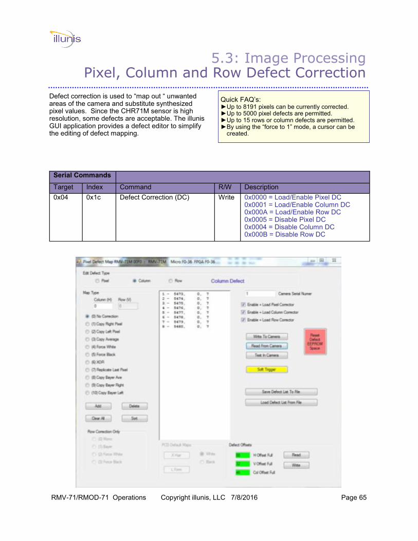
5.3: Image Processing Pixel, Column and Row Defect Correction
Defect correction is used to “map out “ unwanted areas of the camera and substitute synthesized pixel values. Since the CHR71M sensor is high resolution, some defects are acceptable. The illunis GUI application provides a defect editor to simplify the editing of defect mapping.
Serial Commands
Target Index Command R/W Description
0x04 0x1c Defect Correction (DC) Write 0x0000 = Load/Enable Pixel DC 0x0001 = Load/Enable Column DC 0x000A = Load/Enable Row DC 0x0005 = Disable Pixel DC 0x0004 = Disable Column DC 0x000B = Disable Row DC
Quick FAQ’s: ►Up to 8191 pixels can be currently corrected. ►Up to 5000 pixel defects are permitted. ►Up to 15 rows or column defects are permitted. ►By using the “force to 1” mode, a cursor can be
created.
RMV-71/RMOD-71 Operations Copyright illunis, LLC 7/8/2016 Page 66
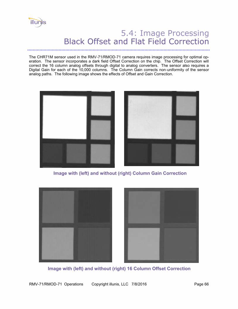
5.4: Image Processing Black Offset and Flat Field Correction
The CHR71M sensor used in the RMV-71/RMOD-71 camera requires image processing for optimal op-eration. The sensor incorporates a dark field Offset Correction on the chip. The Offset Correction will correct the 16 column analog offsets through digital to analog converters. The sensor also requires a Digital Gain for each of the 10,000 columns. The Column Gain corrects non-uniformity of the sensor analog paths. The following image shows the effects of Offset and Gain Correction.
Image with (left) and without (right) Column Gain Correction
Image with (left) and without (right) 16 Column Offset Correction
RMV-71/RMOD-71 Operations Copyright illunis, LLC 7/8/2016 Page 67
Warning: Changing the Flat Field Correction (FFC) tables will impact the
operation of the camera ! Before the user resets the FFC, make sure the current FFC table is saved to a file. The user can save and reload the table using the GUI control program (version 3.0.1). The image processing features of the RMV-71/RMOD-71 camera can be easily setup by using the following: For 16 Column Offset Correction: Use the lens cap or light blocking device. This test is performed in the dark; therefore, no special equipment is needed. Only 16 words of data are stored for this correc-tion. For Column Gain Correction: Use the flat field light source. This can be as simple as a white balance lens cap and a flat background or “s” complex as a programmable light source. The flatter the field pre-sented to the sensor the better the correction will be. The RMV-71/RMOD-71 processes the flat field in two passes, one for the even numbered columns and one for the odd numbered columns. A total of 10,000 Column Gains are calculated and saved in the EEPROM of the camera. This process may take over a minute to complete. For optimum performance, the Offset and Gain calculations should be calculated under the conditions that the camera is used and should include the following parameters:
Operating temperature.
Exposure.
Readout mode and pixel clock speed. It is recommended to perform the Black (offset) calibration first followed by the Bright (gain) calibration. Note: illunis Camera Control Application 2.1.15 (or newer) is required for calibration.
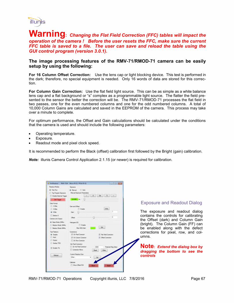
Exposure and Readout Dialog The exposure and readout dialog contains the controls for calibrating the Offset (dark) and Column Gain (bright). The Column Gain (FF) can be enabled along with the defect corrections for pixel, row, and col-umns.
Note: Extend the dialog box by
dragging the bottom to see the controls
RMV-71/RMOD-71 Operations Copyright illunis, LLC 7/8/2016 Page 68
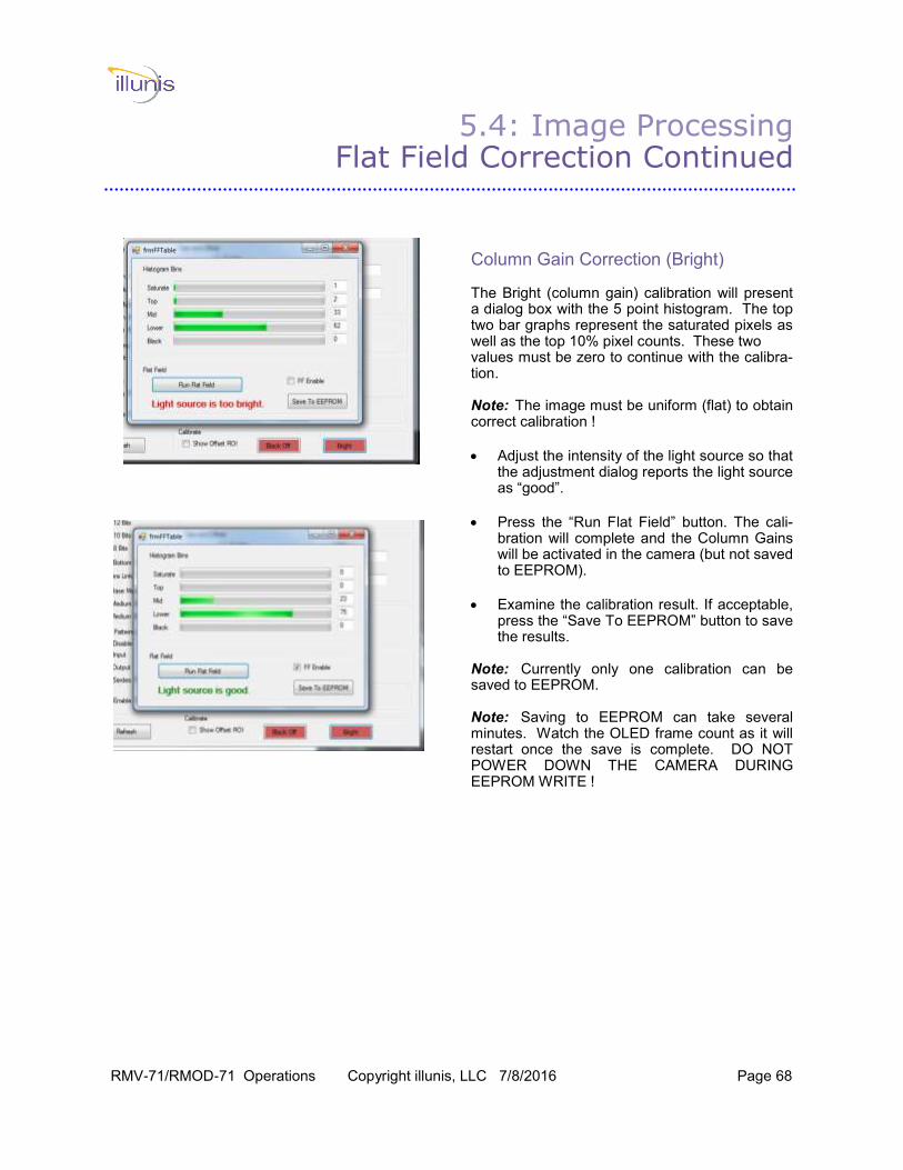
5.4: Image Processing Flat Field Correction Continued
Column Gain Correction (Bright) The Bright (column gain) calibration will present a dialog box with the 5 point histogram. The top two bar graphs represent the saturated pixels as well as the top 10% pixel counts. These two values must be zero to continue with the calibra-tion. Note: The image must be uniform (flat) to obtain correct calibration !
Adjust the intensity of the light source so that the adjustment dialog reports the light source as “good”.
Press the “Run Flat Field” button. The cali-bration will complete and the Column Gains will be activated in the camera (but not saved to EEPROM).
Examine the calibration result. If acceptable, press the “Save To EEPROM” button to save the results.
Note: Currently only one calibration can be saved to EEPROM. Note: Saving to EEPROM can take several minutes. Watch the OLED frame count as it will restart once the save is complete. DO NOT POWER DOWN THE CAMERA DURING EEPROM WRITE !

RMV-71/RMOD-71 Operations Copyright illunis, LLC 7/8/2016 Page 69
5.5: Image Processing Offset Calibration
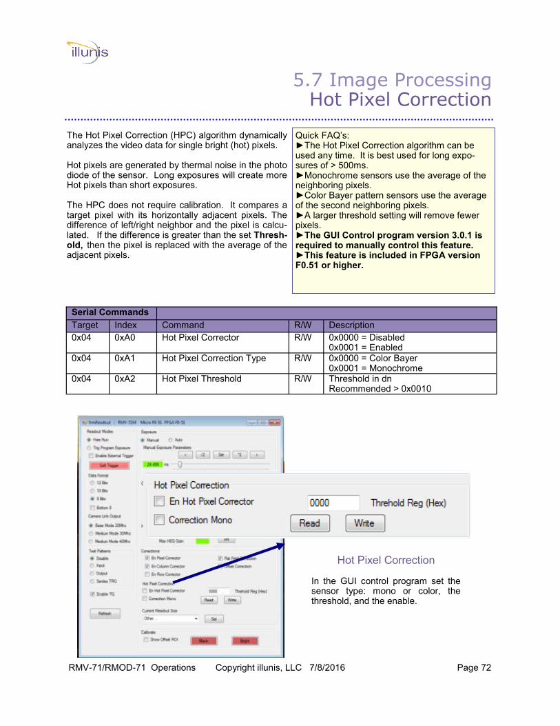
Offset Correction (Black) The Black (offset) calibration will present a dialog box asking the user to cover the lens in order to obtain a completely dark image. Clicking OK will start the Offset Calibration and an on-screen display will be activated to show progress. A series of bar graphs will display the current offset values and relative brightness. As the cali-bration proceeds the values will converge. Once an acceptable solution is found, the calibration data will be saved to EEPROM and the results will display in the OSD. The user may now remove the lens cap and use the camera.
RMV-71/RMOD-71 Operations Copyright illunis, LLC 7/8/2016 Page 70
5.6 Image Processing Automatic Histogram Equalization
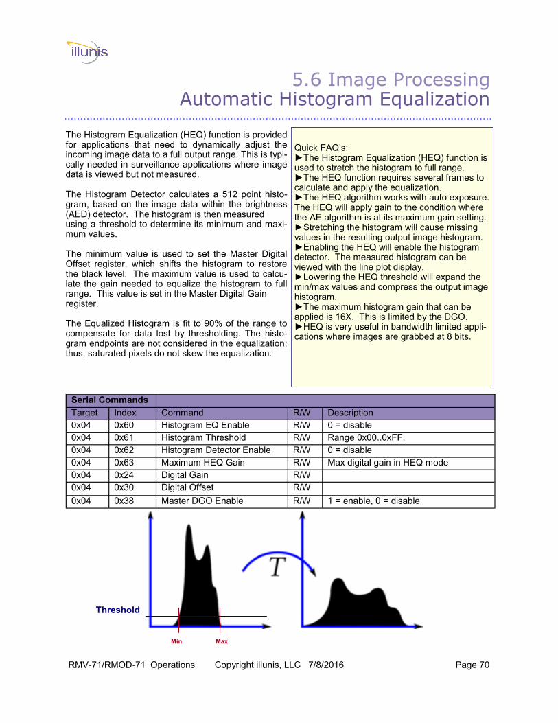
The Histogram Equalization (HEQ) function is provided for applications that need to dynamically adjust the incoming image data to a full output range. This is typi-cally needed in surveillance applications where image data is viewed but not measured. The Histogram Detector calculates a 512 point histo-gram, based on the image data within the brightness (AED) detector. The histogram is then measured using a threshold to determine its minimum and maxi-mum values. The minimum value is used to set the Master Digital Offset register, which shifts the histogram to restore the black level. The maximum value is used to calcu-late the gain needed to equalize the histogram to full range. This value is set in the Master Digital Gain register. The Equalized Histogram is fit to 90% of the range to compensate for data lost by thresholding. The histo-gram endpoints are not considered in the equalization; thus, saturated pixels do not skew the equalization.
Serial Commands
Target Index Command R/W Description
0x04 0x60 Histogram EQ Enable R/W 0 = disable
0x04 0x61 Histogram Threshold R/W Range 0x00..0xFF,
0x04 0x62 Histogram Detector Enable R/W 0 = disable
0x04 0x63 Maximum HEQ Gain R/W Max digital gain in HEQ mode
0x04 0x24 Digital Gain R/W
0x04 0x30 Digital Offset R/W
0x04 0x38 Master DGO Enable R/W 1 = enable, 0 = disable
Quick FAQ’s: ►The Histogram Equalization (HEQ) function is used to stretch the histogram to full range. ►The HEQ function requires several frames to calculate and apply the equalization. ►The HEQ algorithm works with auto exposure. The HEQ will apply gain to the condition where the AE algorithm is at its maximum gain setting. ►Stretching the histogram will cause missing values in the resulting output image histogram. ►Enabling the HEQ will enable the histogram detector. The measured histogram can be viewed with the line plot display. ►Lowering the HEQ threshold will expand the min/max values and compress the output image histogram. ►The maximum histogram gain that can be applied is 16X. This is limited by the DGO. ►HEQ is very useful in bandwidth limited appli-cations where images are grabbed at 8 bits.
Threshold
Min Max

RMV-71/RMOD-71 Operations Copyright illunis, LLC 7/8/2016 Page 71
Low contrast image before Histogram Equalization
Low contrast image after Histogram Equalization
RMV-71/RMOD-71 Operations Copyright illunis, LLC 7/8/2016 Page 72
5.7 Image Processing Hot Pixel Correction
The Hot Pixel Correction (HPC) algorithm dynamically analyzes the video data for single bright (hot) pixels. Hot pixels are generated by thermal noise in the photo diode of the sensor. Long exposures will create more Hot pixels than short exposures. The HPC does not require calibration. It compares a target pixel with its horizontally adjacent pixels. The difference of left/right neighbor and the pixel is calcu-lated. If the difference is greater than the set Thresh-old, then the pixel is replaced with the average of the adjacent pixels.
Serial Commands
Target Index Command R/W Description
0x04 0xA0 Hot Pixel Corrector R/W 0x0000 = Disabled 0x0001 = Enabled
0x04 0xA1 Hot Pixel Correction Type R/W 0x0000 = Color Bayer 0x0001 = Monochrome
0x04 0xA2 Hot Pixel Threshold R/W Threshold in dn Recommended > 0x0010
Quick FAQ’s: ►The Hot Pixel Correction algorithm can be used any time. It is best used for long expo-sures of > 500ms. ►Monochrome sensors use the average of the neighboring pixels. ►Color Bayer pattern sensors use the average of the second neighboring pixels. ►A larger threshold setting will remove fewer pixels. ►The GUI Control program version 3.0.1 is required to manually control this feature. ►This feature is included in FPGA version F0.51 or higher.
Hot Pixel Correction In the GUI control program set the sensor type: mono or color, the threshold, and the enable.
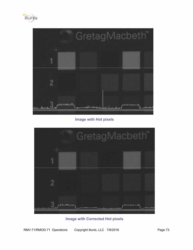
RMV-71/RMOD-71 Operations Copyright illunis, LLC 7/8/2016 Page 73
Image with Hot pixels
Image with Corrected Hot pixels
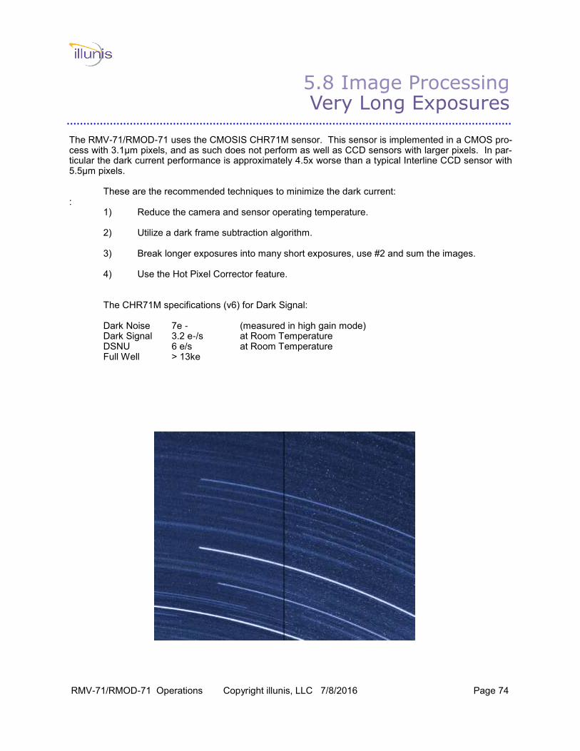
RMV-71/RMOD-71 Operations Copyright illunis, LLC 7/8/2016 Page 74
5.8 Image Processing Very Long Exposures
The RMV-71/RMOD-71 uses the CMOSIS CHR71M sensor. This sensor is implemented in a CMOS pro-cess with 3.1µm pixels, and as such does not perform as well as CCD sensors with larger pixels. In par-ticular the dark current performance is approximately 4.5x worse than a typical Interline CCD sensor with 5.5µm pixels. These are the recommended techniques to minimize the dark current: : 1) Reduce the camera and sensor operating temperature. 2) Utilize a dark frame subtraction algorithm. 3) Break longer exposures into many short exposures, use #2 and sum the images. 4) Use the Hot Pixel Corrector feature. The CHR71M specifications (v6) for Dark Signal: Dark Noise 7e - (measured in high gain mode) Dark Signal 3.2 e-/s at Room Temperature DSNU 6 e/s at Room Temperature Full Well > 13ke
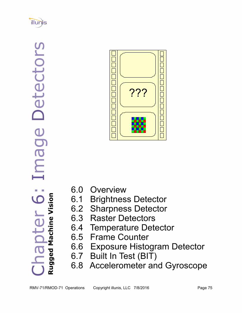
RMV-71/RMOD-71 Operations Copyright illunis, LLC 7/8/2016 Page 75
Chapte
r 6:
Image D
ete
cto
rs
Ru
gg
ed
Mach
ine V
isio
n 6.0 Overview
6.1 Brightness Detector 6.2 Sharpness Detector 6.3 Raster Detectors 6.4 Temperature Detector 6.5 Frame Counter 6.6 Exposure Histogram Detector 6.7 Built In Test (BIT) 6.8 Accelerometer and Gyroscope
???
RMV-71/RMOD-71 Operations Copyright illunis, LLC 7/8/2016 Page 76
6.0: Image Detectors Overview
The RMV-71/RMOD-71 camera incorporates several video "detectors" that analyze imagery in real time. The video detectors measure exposure, focus, SNR, and raster size. The exposure detectors operate in several modes that allow the measurement of image brightness. The focus detectors measure the sharpness of the image and can be used for auto focus optics. In addition to the detec-tors, the windows of the detectors can be overlaid on the video image. Note: When using the windowing modes, the detector window is automatically reset to fit the window. The default windows cover 90% of the image area.
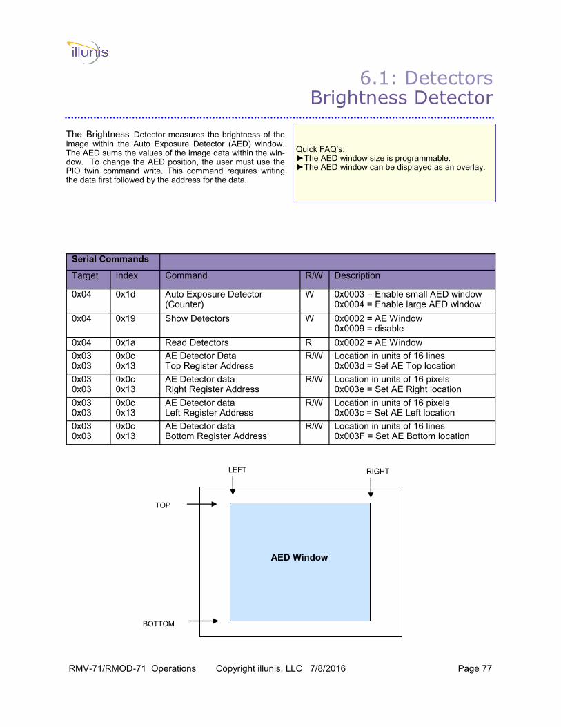
RMV-71/RMOD-71 Operations Copyright illunis, LLC 7/8/2016 Page 77
6.1: Detectors Brightness Detector
The Brightness Detector measures the brightness of the image within the Auto Exposure Detector (AED) window. The AED sums the values of the image data within the win-dow. To change the AED position, the user must use the PIO twin command write. This command requires writing the data first followed by the address for the data.
Serial Commands
Target Index Command R/W Description
0x04 0x1d Auto Exposure Detector (Counter)
W 0x0003 = Enable small AED window 0x0004 = Enable large AED window
0x04 0x19 Show Detectors W 0x0002 = AE Window 0x0009 = disable
0x04 0x1a Read Detectors R 0x0002 = AE Window
0x03 0x03
0x0c 0x13
AE Detector Data Top Register Address
R/W Location in units of 16 lines 0x003d = Set AE Top location
0x03 0x03
0x0c 0x13
AE Detector data Right Register Address
R/W Location in units of 16 pixels 0x003e = Set AE Right location
0x03 0x03
0x0c 0x13
AE Detector data Left Register Address
R/W Location in units of 16 pixels 0x003c = Set AE Left location
0x03 0x03
0x0c 0x13
AE Detector data Bottom Register Address
R/W Location in units of 16 lines 0x003F = Set AE Bottom location
Quick FAQ’s: ►The AED window size is programmable. ►The AED window can be displayed as an overlay.
AED Window
TOP
BOTTOM
LEFT RIGHT

RMV-71/RMOD-71 Operations Copyright illunis, LLC 7/8/2016 Page 78
6.2: Detectors Sharpness Detector
The Sharpness Detector uses AED window. The Sharpness Detector can be used as an Auto Focus Detector (AFD). The AFD calculates sharpness as the summation of the difference of the pixels within the win-dow.
Serial Commands
Target Index Command R/W Description
0x04 0x19 Show Detectors W 0x0003 = AF Window 0x0007 = AF Data in AF Window 0x0008 = AF Data Full Screen 0x0009 = disable
0x04 0x1a Read Detectors R 0x0003 = AF Window
Quick FAQ’s: ►The AFD window is the same as the AED win-
dow ! ►The AFD window can be displayed as an overlay. ►The AFD data can be displayed as video data
showing either the first or second derivative. ►The AF value peaks sharply when the image is at
its maximum sharpness.
AFD Detector Derivative Image (whole screen)
Maximum Sharpness
Detector Value
Lens Focus Position

RMV-71/RMOD-71 Operations Copyright illunis, LLC 7/8/2016 Page 79
6.3: Detectors Raster Detectors
The Raster Detectors (RD) are used to measure the size of the video image output by the RMV-71/RMOD-71 Camera Link signals. The RD’s count the number of pix-els per line and the number of active pixels per line. The RD’s also count the number of lines per frame and the number of active lines per frame. Because the RMV-71/RMOD-71 can be set to any number of modes, the RD circuit is vital to correctly configuring the capture device.
Serial Commands
Target Index Command R/W Description
0x04 0x1b System Registers R 0x0000 = Read Pixels/Line 0x0001 = Read Active Pixels/Line (in LVAL) 0x0002 = Read Lines per Frame 0x0003 = Read Active Lines per Frame (in FVAL)
0x04 0x14 Line of Interest R/W Line number from top of image (Plus FVAL start)
Quick FAQ’s: ►LVAL = Line VALid: This Camera Link signal indi-
cates when pixel data is valid with a line. ►FVAL = Frame VALid: This Camera Link signal
indicates when line data is valid with a frame. ►LVAL start and stop define a lines active pixels and
are in an unusual internal FPGA counting unit. ►FVAL start and stop define a frames active lines
and are directly related to the sensor design. ►The Raster Line Detectors use the “line of inter-
est” line from the On Screen line plot function to determine which line is measured. The “line of interest” must be in the visible image data or the detectors will read zero !
Active Area
Active Pixels Per Line
Active L
ines P
er
Fra
me
Pixels Per Line
Lin
es P
er
Fra
me
FV
AL
LVAL
RMV-71/RMOD-71 Operations Copyright illunis, LLC 7/8/2016 Page 80
6.4: Detectors Temperature Detector
The temperature of the RMV-71/RMOD-71 camera is obtained though a solid state device located on the main PCB. The temperature sensor is located as close as possible to the warmest component in the camera. The temperature sensor does not read the sensor temperature !
Serial Commands
Target Index Command R/W Description
0x04 0x07 Camera Temperature R Temperature in degrees Celsius
0x5C 0x02 Sensor Internal Temperature R Temperature in degrees Celsius
Quick FAQ’s: ►Temperature is read in degrees Celsius. ►Temperature accuracy is 0.5 degrees.
6.5: Detectors Frame Counter
A Frame Counter is implemented in the RMV-71/RMOD-71 FPGA. Each frame read has a unique count. The user can read the frame count immediately after the rising edge of FVAL. The Frame Counter is displayed in the On Screen Display of the camera parameters.
Serial Commands
Target Index Command R/W Description
0x04 0x1A Read Detector R 0x000A = Frame Counter 0x04 0x1A Reset Frame Counter to Zero W 0x000A = Reset to Zero
Quick FAQ’s: ►The Frame Counter is a 16 bit counter that rolls
over to zero when the maximum count of 65535 is reached.
Example: Read 0x003D = 61(decimal) degrees Celsius

RMV-71/RMOD-71 Operations Copyright illunis, LLC 7/8/2016 Page 81
6.6: Detectors Exposure Histogram Detector
The Brightness Detector is used to measure the brightness of the image within the Auto Exposure Detector (AED) win-dow.
The Exposure Histogram Detector is used to measure the number of pixels at specific brightness levels through the concept of bins. Bins are used to count the number of pix-els within two ADC values that occur in the AED window. The bin sizes are determined by three register values that define points in the ADC count. There are five bins. The typical usage of the bins are: BIN0 is used for black meas-urement, BIN1 and BIN2 are used to measure mid range, BIN3 is used to measure bright points, and BIN4 is used to measure saturated pixels.
In addition to the histogram bin counts, a reference count of the number of pixels in the AED window is provided. This reference count can be used easily to calculate percent-ages of pixel counts within the bins.
Serial Commands
Target Index Command R/W Description
0x04 0x1a Read Bin and AED size values R 0x0011 = Bin #0 0x0012 = Bin #1 0x0013 = Bin #2 0x0014 = Bin #3 0x0015 = Bin #4 = # sat pixels 0x0016 = Number of pixels in
0x03 0x03
0x0c 0x13
AE Histogram Point Register Address
R/W Location in histogram bin point in units of 16 DN 0x004A = Set AEH point #1 0x004B = Set AEH point #2 0x004C = Set AEH point #3
0x04 0x19 Show Detectors W 0x000A = Blooming 0x0009 = disable
Quick FAQ’s: ►The Saturated Pixel Counter (SPC) uses bin 4. ►The bin register values are in units of 16 DN. ►The PT1 value is usually 4X the black clamp. ►The PT2 value is usually one half the max count. ►The PT3 value is usually 85% the max count. ►Typical register values for the points are: PT1: 0x08 = 0x08 * 16dec = 128 dec DN PT2: 0x80 = 0x80 * 16dec = 2048 dec DN PT3: 0xE0 = 0xE0 * 16dec = 3568 dec DN ►The Detector OSD, displays the bin counts and a
new bar graph display.
0 4095
Pix
els
@ D
N
DN
PT1 PT2 PT3 PT4 = 4094
BIN
0
BIN
1
BIN
2
BIN
3
BIN
4
RMV-71/RMOD-71 Operations Copyright illunis, LLC 7/8/2016 Page 82
6.7: Detectors Built In Test
The RMV-71/RMOD-71 camera includes several self-test features.
Serial Commands
Target Index Command R/W Description
0x99 0x00 System Error R 0x0000 = No Error 0x0001 = Brown out 0x0002 = Watchdog timer reset 0x0003 = UART Error 0x0004 = VSYNC Timeout 0x0005 = Serdes Error 0x0006 = FPGA Configuration Error 0x0007 = SPI Error 0x0008 = EEPROM Error 0x0009 = Voltage Regulator Error
0x99 0x01 Calculate Internal Voltages R Returns nothing
0x99 0x02 Return 1.8V (A) R Voltage * 10
0x99 0x03 Return 1.8V (B) R Voltage * 10
0x99 0x04 Return 5V R Voltage * 10
0x99 0x05 Return 3V R Voltage * 10
0x99 0x06 Return 2.5V R Voltage * 10
0x99 0x07 Return 1.2V R Voltage * 10
0x99 0x08 Return Input V R Voltage * 10
0x99 0x0C Return 1.8V (A) Error R Voltage * 10
0x99 0x0D Return 1.8V (B) Error R Voltage * 10
0x99 0x0E Return 5V Error R Voltage * 10
0x99 0x0F Return 3V Error R Voltage * 10
0x99 0x10 Return 2.5V Error R Voltage * 10
0x99 0x11 Return 1.2V Error R Voltage * 10
0x99 0x12 Return Input V Error R Voltage * 10
Quick FAQ’s: ►Internal testing is useful for mission critical opera-
tions !
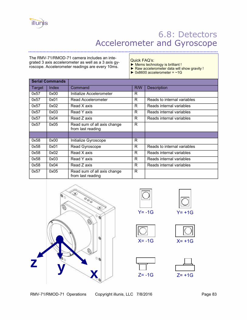
RMV-71/RMOD-71 Operations Copyright illunis, LLC 7/8/2016 Page 83
6.8: Detectors Accelerometer and Gyroscope
The RMV-71/RMOD-71 camera includes an inte-grated 3 axis accelerometer as well as a 3 axis gy-roscope. Accelerometer readings are every 10ms.
Serial Commands
Target Index Command R/W Description
0x57 0x00 Initialize Accelerometer R
0x57 0x01 Read Accelerometer R Reads to internal variables
0x57 0x02 Read X axis R Reads internal variables
0x57 0x03 Read Y axis R Reads internal variables
0x57 0x04 Read Z axis R Reads internal variables
0x57 0x05 Read sum of all axis change from last reading
R
0x58 0x00 Initialize Gyroscope R
0x58 0x01 Read Gyroscope R Reads to internal variables
0x58 0x02 Read X axis R Reads internal variables
0x58 0x03 Read Y axis R Reads internal variables
0x58 0x04 Read Z axis R Reads internal variables
0x57 0x05 Read sum of all axis change from last reading
R
Quick FAQ’s: ► Mems technology is brilliant ! ► Raw accelerometer data will show gravity ! ► 0x8600 accelerometer = ~1G
x y z
Y= -1G Y= +1G
X= -1G X= +1G
Z= -1G Z= +1G

RMV-71/RMOD-71 Operations Copyright illunis, LLC 7/8/2016 Page 84
Chapte
r 7:
OSD
ispla
ys
Ru
gg
ed
Mach
ine V
isio
n
7.0 OSDisplay Overview 7.1 On Screen Text Display 7.2 On Screen Line Plot 7.3 On Screen Column Plot 7.4 Synthetic Test Patterns 7.5 Detector Window Display 7.6 Histogram Plot 7.7 OLED
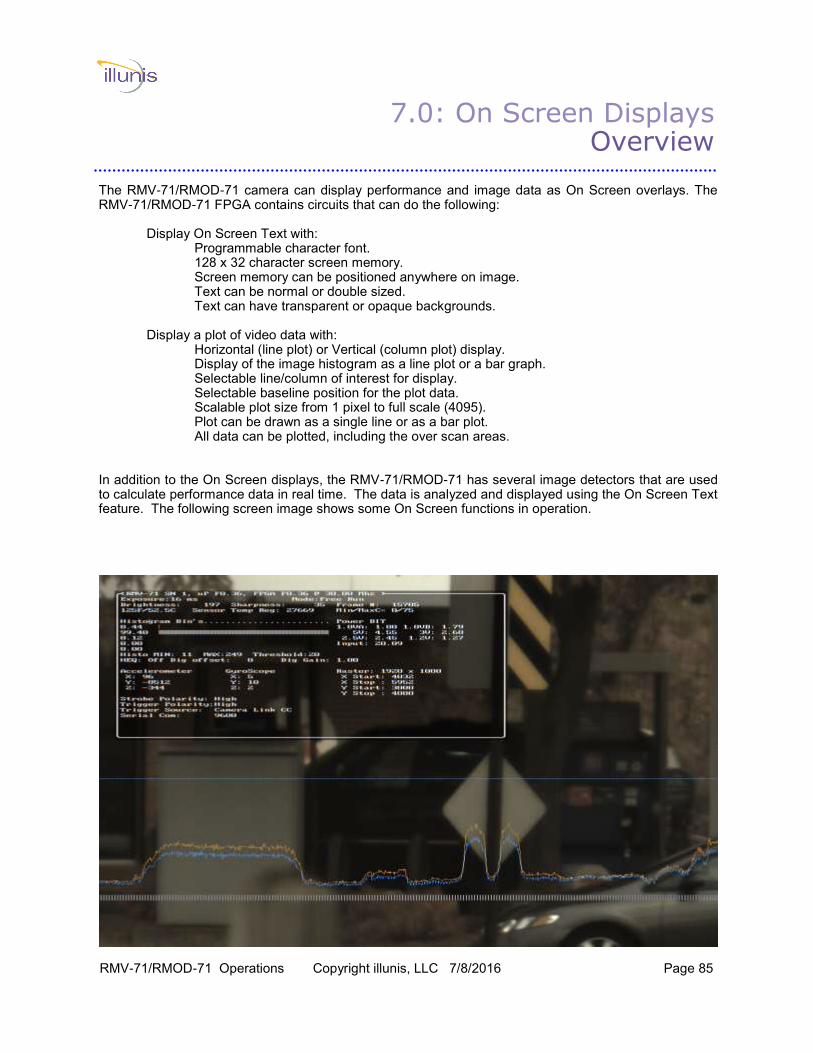
RMV-71/RMOD-71 Operations Copyright illunis, LLC 7/8/2016 Page 85
7.0: On Screen Displays Overview
The RMV-71/RMOD-71 camera can display performance and image data as On Screen overlays. The RMV-71/RMOD-71 FPGA contains circuits that can do the following:
Display On Screen Text with: Programmable character font. 128 x 32 character screen memory. Screen memory can be positioned anywhere on image. Text can be normal or double sized. Text can have transparent or opaque backgrounds. Display a plot of video data with: Horizontal (line plot) or Vertical (column plot) display. Display of the image histogram as a line plot or a bar graph. Selectable line/column of interest for display. Selectable baseline position for the plot data. Scalable plot size from 1 pixel to full scale (4095). Plot can be drawn as a single line or as a bar plot. All data can be plotted, including the over scan areas.
In addition to the On Screen displays, the RMV-71/RMOD-71 has several image detectors that are used to calculate performance data in real time. The data is analyzed and displayed using the On Screen Text feature. The following screen image shows some On Screen functions in operation.
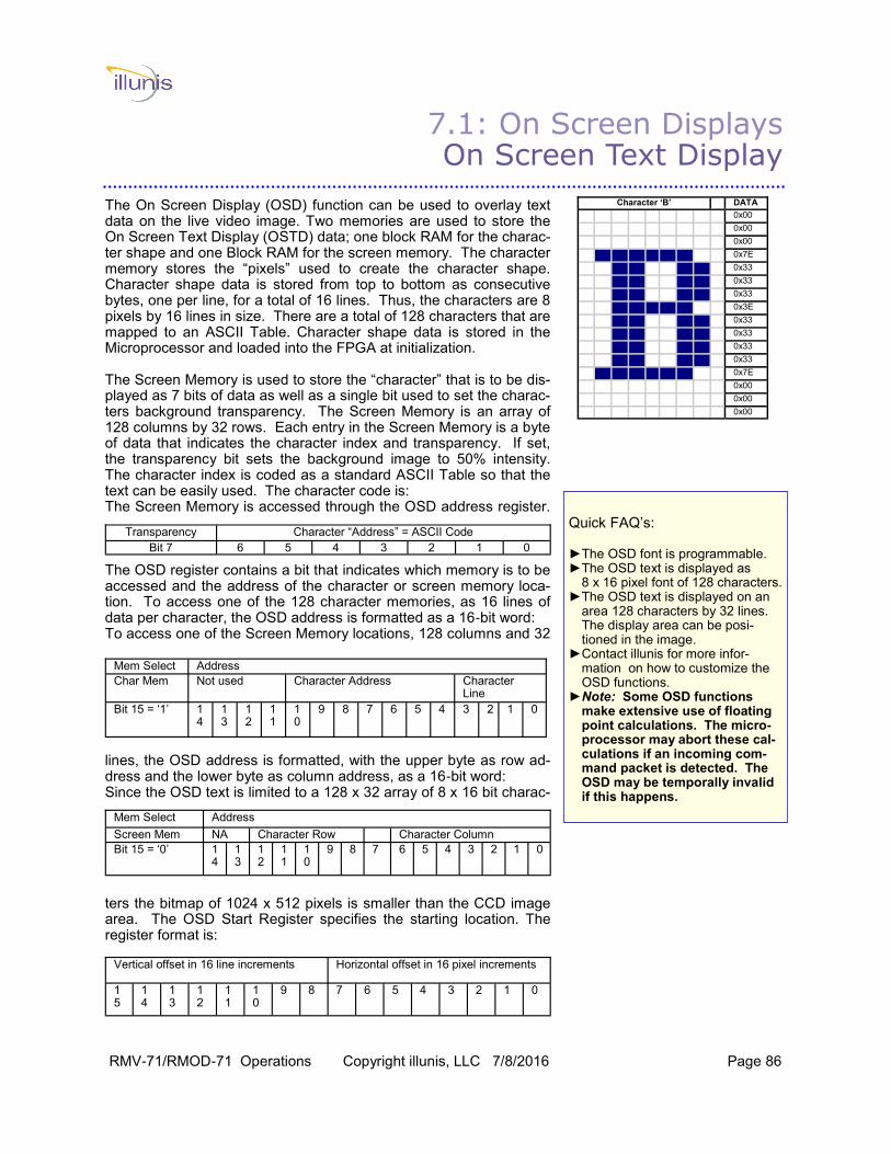
RMV-71/RMOD-71 Operations Copyright illunis, LLC 7/8/2016 Page 86
7.1: On Screen Displays On Screen Text Display
The On Screen Display (OSD) function can be used to overlay text data on the live video image. Two memories are used to store the On Screen Text Display (OSTD) data; one block RAM for the charac-ter shape and one Block RAM for the screen memory. The character memory stores the “pixels” used to create the character shape. Character shape data is stored from top to bottom as consecutive bytes, one per line, for a total of 16 lines. Thus, the characters are 8 pixels by 16 lines in size. There are a total of 128 characters that are mapped to an ASCII Table. Character shape data is stored in the Microprocessor and loaded into the FPGA at initialization.
The Screen Memory is used to store the “character” that is to be dis-played as 7 bits of data as well as a single bit used to set the charac-ters background transparency. The Screen Memory is an array of 128 columns by 32 rows. Each entry in the Screen Memory is a byte of data that indicates the character index and transparency. If set, the transparency bit sets the background image to 50% intensity. The character index is coded as a standard ASCII Table so that the text can be easily used. The character code is: The Screen Memory is accessed through the OSD address register.
The OSD register contains a bit that indicates which memory is to be accessed and the address of the character or screen memory loca-tion. To access one of the 128 character memories, as 16 lines of data per character, the OSD address is formatted as a 16-bit word: To access one of the Screen Memory locations, 128 columns and 32
lines, the OSD address is formatted, with the upper byte as row ad-dress and the lower byte as column address, as a 16-bit word: Since the OSD text is limited to a 128 x 32 array of 8 x 16 bit charac-
ters the bitmap of 1024 x 512 pixels is smaller than the CCD image area. The OSD Start Register specifies the starting location. The register format is:
Quick FAQ’s: ►The OSD font is programmable. ►The OSD text is displayed as
8 x 16 pixel font of 128 characters. ►The OSD text is displayed on an
area 128 characters by 32 lines. The display area can be posi-tioned in the image.
►Contact illunis for more infor-mation on how to customize the OSD functions.
►Note: Some OSD functions make extensive use of floating point calculations. The micro- processor may abort these cal-culations if an incoming com-mand packet is detected. The OSD may be temporally invalid if this happens.
Character ‘B’ DATA
0x00
0x00
0x00
0x7E
0x33
0x33
0x33
0x3E
0x33
0x33
0x33
0x33
0x7E
0x00
0x00
0x00
Transparency Character “Address” = ASCII Code
Bit 7 6 5 4 3 2 1 0
Mem Select Address
Char Mem Not used Character Address Character Line
Bit 15 = ‘1’ 14
13
12
11
10
9 8 7 6 5 4 3 2 1 0
Mem Select Address
Screen Mem NA Character Row Character Column
Bit 15 = ‘0’ 14
13
12
11
10
9 8 7 6 5 4 3 2 1 0
Vertical offset in 16 line increments Horizontal offset in 16 pixel increments
15
14
13
12
11
10
9 8 7 6 5 4 3 2 1 0

RMV-71/RMOD-71 Operations Copyright illunis, LLC 7/8/2016 Page 87
Serial Commands
Target Index Command R/W Description
0x04 0x15 OSD Text W 0x0000 disable text overlay (All) 0x0001 enable OSD (Detectors) 0x0002 update display window 0x0003 enable 2X window 0x0004 disable 2X window 0x0005 enable OSD (Raster) 0x0006 enable OSD (Revision) 0x0007 enable OSD (Frame Counter)
0x04 0x16 ODS Text Window X location R/W Increments of 128 pixels
0x04 0x17 OSD Text Window Y location R/W Increments of 64 lines
0x12 Char Font pattern W Custom Font Entry
0x13 Char Data = HHVV W HH = horizontal (byte) VV = vertical (byte)
0x16 0x00 OSD Initialize W
0x16 0x01 OSD Screen clear W
0x16 0x02 OSC Test pattern
Character ‘B’ DATA
0x00
0x00
0x00
0x7E
0x33
0x33
0x33
0x3E
0x33
0x33
0x33
0x33
0x7E
0x00
0x00
0x00
Example Custom Char…. ‘B’ = 0x42 ascii, write 16 entries
{w1242000000} {w1242000000} {w1242000000} {w1242007Ecs} {w12420033cs}
…. {w1242000000}
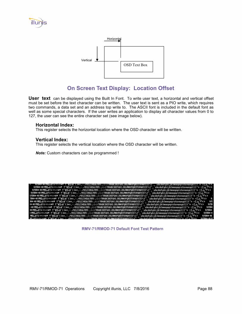
RMV-71/RMOD-71 Operations Copyright illunis, LLC 7/8/2016 Page 88
User text can be displayed using the Built In Font. To write user text, a horizontal and vertical offset must be set before the text character can be written. The user text is sent as a PIO write, which requires two commands, a data set and an address top write to. The ASCII font is included in the default font as well as some special characters. If the user writes an application to display all character values from 0 to 127, the user can see the entire character set (see image below).
Horizontal Index: This register selects the horizontal location where the OSD character will be written.
Vertical Index: This register selects the vertical location where the OSD character will be written. Note: Custom characters can be programmed !
RMV-71/RMOD-71 Default Font Test Pattern
OSD Text Box
Horizontal
Vertical
On Screen Text Display: Location Offset
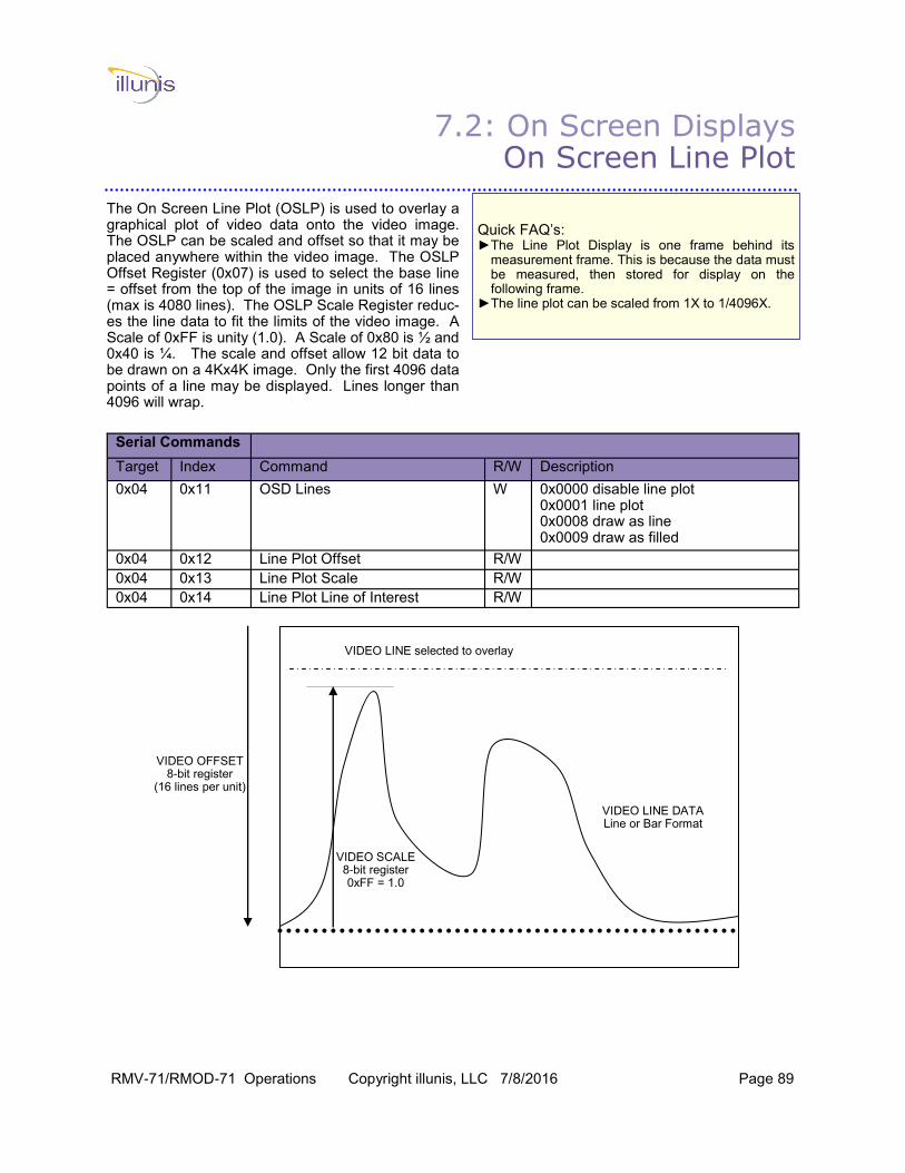
RMV-71/RMOD-71 Operations Copyright illunis, LLC 7/8/2016 Page 89
7.2: On Screen Displays On Screen Line Plot
The On Screen Line Plot (OSLP) is used to overlay a graphical plot of video data onto the video image. The OSLP can be scaled and offset so that it may be placed anywhere within the video image. The OSLP Offset Register (0x07) is used to select the base line = offset from the top of the image in units of 16 lines (max is 4080 lines). The OSLP Scale Register reduc-es the line data to fit the limits of the video image. A Scale of 0xFF is unity (1.0). A Scale of 0x80 is ½ and 0x40 is ¼. The scale and offset allow 12 bit data to be drawn on a 4Kx4K image. Only the first 4096 data points of a line may be displayed. Lines longer than 4096 will wrap.
Serial Commands
Target Index Command R/W Description
0x04 0x11 OSD Lines W 0x0000 disable line plot 0x0001 line plot 0x0008 draw as line 0x0009 draw as filled
0x04 0x12 Line Plot Offset R/W 0x04 0x13 Line Plot Scale R/W 0x04 0x14 Line Plot Line of Interest R/W
Quick FAQ’s: ►The Line Plot Display is one frame behind its
measurement frame. This is because the data must be measured, then stored for display on the following frame.
►The line plot can be scaled from 1X to 1/4096X.
VIDEO OFFSET 8-bit register
(16 lines per unit)
VIDEO LINE selected to overlay
VIDEO SCALE 8-bit register 0xFF = 1.0
VIDEO LINE DATA Line or Bar Format

RMV-71/RMOD-71 Operations Copyright illunis, LLC 7/8/2016 Page 90
7.3: On Screen Displays On Screen Column Plot
The On Screen Column Plot (OSCP) is used to overlay a graphical plot of video data onto the video image. The OSCP functions are similar to the OSLP except in the vertical direction.
Serial Commands
Target Index Command R/W Description
0x04 0x11 OSD Lines W 0x0000 disable line plot 0x0002 column 0x0008 draw as line 0x0009 draw as filled
0x04 0x12 Line Plot Offset R/W 0x04 0x13 Line Plot Scale R/W 0x04 0x14 Line Plot Line of Interest R/W
Quick FAQ’s: ►The Column Plot Display is one frame behind its
measurement frame. This is because the data must be measured and then stored for display on the following frame.
►The line column can be scaled from 1X to 1/4096X: 4096 pixels to 1 pixel.
VIDEO OFFSET 8-bit register
(16 lines per unit)
VID
EO
LIN
E s
ele
cte
d to o
verla
y
VIDEO SCALE 8-bit register 0xFF = 1.0
1.0 = 4096 Max
VID
EO
CO
LU
MN
D
AT
A
Lin
e o
r B
ar
Fo
rmat

RMV-71/RMOD-71 Operations Copyright illunis, LLC 7/8/2016 Page 91
7.4: On Screen Displays Synthetic Test Patterns
The RMV-71/RMOD-71 camera has two synthetic test patterns that can be used for testing both the digital path and Camera Link communications.
Serial Commands
Target Index Command R/W Description
0x04 0x06 Test Pattern
W 0x0000 = Normal Video 0x0001 = Input (CCD) Test Pattern 0x0002 = Output Test Pattern
Quick FAQ’s: ►The Input Test Pattern can be used to test the in-
ternal data path of the RMV-71/RMOD-71 FPGA. ►The Output Test Pattern can be used to test the
Camera Link digital communication path.
Output Test Pattern
Input (CCD) Test Pattern
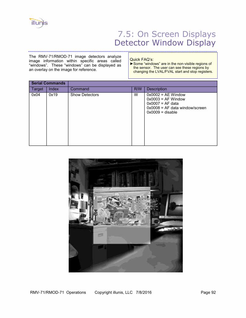
RMV-71/RMOD-71 Operations Copyright illunis, LLC 7/8/2016 Page 92
7.5: On Screen Displays Detector Window Display
The RMV-71/RMOD-71 image detectors analyze image information within specific areas called “windows”. These “windows” can be displayed as an overlay on the image for reference.
Serial Commands
Target Index Command R/W Description
0x04 0x19 Show Detectors W 0x0002 = AE Window 0x0003 = AF Window 0x0007 = AF data 0x0008 = AF data window/screen 0x0009 = disable
Quick FAQ’s: ►Some “windows” are in the non-visible regions of
the sensor. The user can see these regions by changing the LVAL/FVAL start and stop registers.
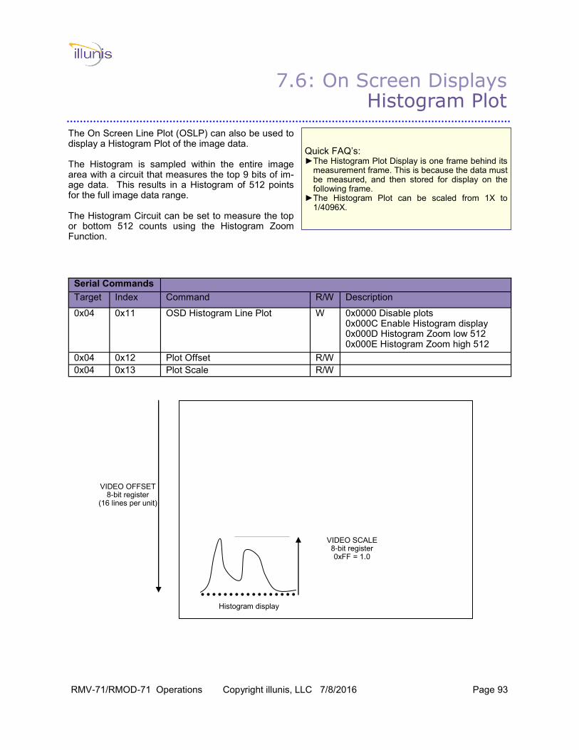
RMV-71/RMOD-71 Operations Copyright illunis, LLC 7/8/2016 Page 93
7.6: On Screen Displays Histogram Plot
The On Screen Line Plot (OSLP) can also be used to display a Histogram Plot of the image data.
The Histogram is sampled within the entire image area with a circuit that measures the top 9 bits of im-age data. This results in a Histogram of 512 points for the full image data range.
The Histogram Circuit can be set to measure the top or bottom 512 counts using the Histogram Zoom Function.
Serial Commands
Target Index Command R/W Description
0x04 0x11 OSD Histogram Line Plot W 0x0000 Disable plots 0x000C Enable Histogram display 0x000D Histogram Zoom low 512 0x000E Histogram Zoom high 512
0x04 0x12 Plot Offset R/W 0x04 0x13 Plot Scale R/W
Quick FAQ’s: ►The Histogram Plot Display is one frame behind its
measurement frame. This is because the data must be measured, and then stored for display on the following frame.
►The Histogram Plot can be scaled from 1X to 1/4096X.
VIDEO OFFSET 8-bit register
(16 lines per unit)
Histogram display
VIDEO SCALE 8-bit register 0xFF = 1.0

RMV-71/RMOD-71 Operations Copyright illunis, LLC 7/8/2016 Page 94
7.7: On Screen Displays
OLED
The On Screen Display (OLED) screen on the RMV-71 camera is used to display internal data as well as show firmware loading status.
Quick FAQ’s: ► The OLED operation can cause minute amounts of
noise in the very lowest bits of the image; there-fore, an option to disable it is provided.
Serial Commands
Target Index Command R/W Description
0x5F 0x00 Select OLED Screen W 0x0000 = BOOT 0x0001 = Main 0x0002 = Detectors 0x0003 = AFE 0x0004 = Built In Test 0x0006 = Accel and Gyro 0x0007 = Off
0x5F 0x01 Put Character W Char 0x5F 0x02 Clear Screen W
0x5F 0x03 Move Cursor W 0xHHVV
0x5F 0x04 Text Foreground Color W
0x5F 0x05 Text Width W In X time (1 = default)
0x5F 0x06 Text Height W In X times
0x5F 0x07 Text Bold W
0x5F 0x08 Clear Line W Line #
RMV-71/RMOD-71 Operations Copyright illunis, LLC 7/8/2016 Page 95
Chapte
r 8:
Cam
era
Lin
k
Ru
gg
ed
Mach
ine V
isio
n
8.0 Camera Link Overview 8.1 Pixel Format 8.2 Channel Format 8.3 Camera Link Valids 8.4 Raster & Exposure Detectors 8.5 Coreco CamExpert Setup 8.6 Matrox Intellicam Setup 8.7 Power Over Camera Link
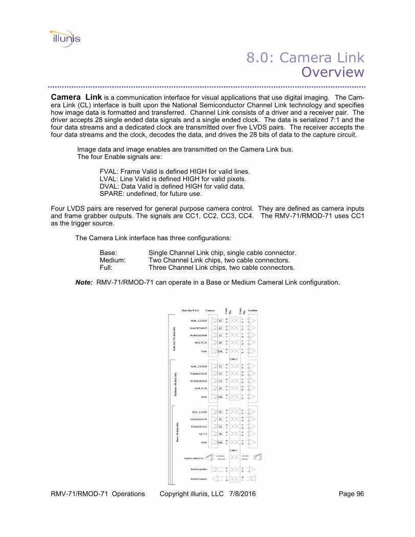
RMV-71/RMOD-71 Operations Copyright illunis, LLC 7/8/2016 Page 96
8.0: Camera Link Overview
Camera Link is a communication interface for visual applications that use digital imaging. The Cam-era Link (CL) interface is built upon the National Semiconductor Channel Link technology and specifies how image data is formatted and transferred. Channel Link consists of a driver and a receiver pair. The driver accepts 28 single ended data signals and a single ended clock. The data is serialized 7:1 and the four data streams and a dedicated clock are transmitted over five LVDS pairs. The receiver accepts the four data streams and the clock, decodes the data, and drives the 28 bits of data to the capture circuit.
Image data and image enables are transmitted on the Camera Link bus. The four Enable signals are: FVAL: Frame Valid is defined HIGH for valid lines. LVAL: Line Valid is defined HIGH for valid pixels. DVAL: Data Valid is defined HIGH for valid data. SPARE: undefined, for future use.
Four LVDS pairs are reserved for general purpose camera control. They are defined as camera inputs and frame grabber outputs. The signals are CC1, CC2, CC3, CC4. The RMV-71/RMOD-71 uses CC1 as the trigger source.
The Camera Link interface has three configurations: Base: Single Channel Link chip, single cable connector. Medium: Two Channel Link chips, two cable connectors. Full: Three Channel Link chips, two cable connectors.
Note: RMV-71/RMOD-71 can operate in a Base or Medium Cameral Link configuration.
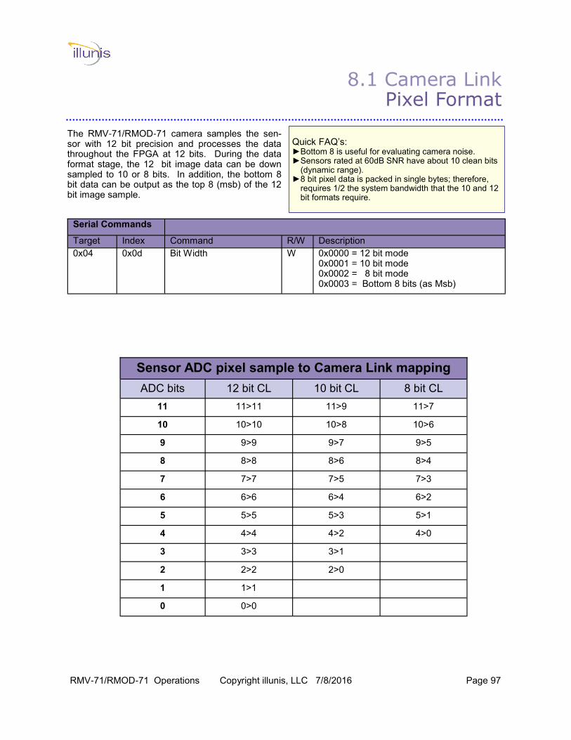
RMV-71/RMOD-71 Operations Copyright illunis, LLC 7/8/2016 Page 97
8.1 Camera Link Pixel Format
The RMV-71/RMOD-71 camera samples the sen-sor with 12 bit precision and processes the data throughout the FPGA at 12 bits. During the data format stage, the 12 bit image data can be down sampled to 10 or 8 bits. In addition, the bottom 8 bit data can be output as the top 8 (msb) of the 12 bit image sample.
Serial Commands
Target Index Command R/W Description
0x04 0x0d Bit Width W 0x0000 = 12 bit mode 0x0001 = 10 bit mode 0x0002 = 8 bit mode 0x0003 = Bottom 8 bits (as Msb)
Quick FAQ’s: ►Bottom 8 is useful for evaluating camera noise. ►Sensors rated at 60dB SNR have about 10 clean bits
(dynamic range). ►8 bit pixel data is packed in single bytes; therefore,
requires 1/2 the system bandwidth that the 10 and 12 bit formats require.
Sensor ADC pixel sample to Camera Link mapping
ADC bits 12 bit CL 10 bit CL 8 bit CL
11 11>11 11>9 11>7
10 10>10 10>8 10>6
9 9>9 9>7 9>5
8 8>8 8>6 8>4
7 7>7 7>5 7>3
6 6>6 6>4 6>2
5 5>5 5>3 5>1
4 4>4 4>2 4>0
3 3>3 3>1
2 2>2 2>0
1 1>1
0 0>0
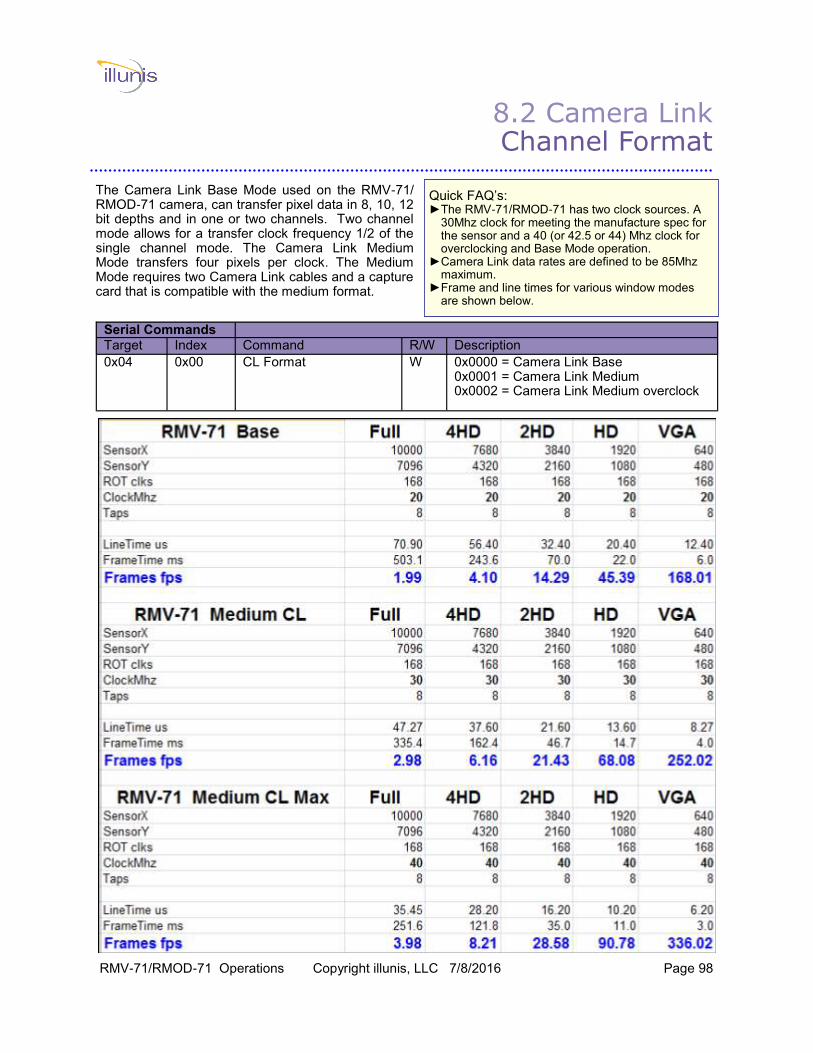
RMV-71/RMOD-71 Operations Copyright illunis, LLC 7/8/2016 Page 98
8.2 Camera Link Channel Format
The Camera Link Base Mode used on the RMV-71/RMOD-71 camera, can transfer pixel data in 8, 10, 12 bit depths and in one or two channels. Two channel mode allows for a transfer clock frequency 1/2 of the single channel mode. The Camera Link Medium Mode transfers four pixels per clock. The Medium Mode requires two Camera Link cables and a capture card that is compatible with the medium format.
Serial Commands
Target Index Command R/W Description
0x04 0x00 CL Format W 0x0000 = Camera Link Base 0x0001 = Camera Link Medium 0x0002 = Camera Link Medium overclock
Quick FAQ’s: ►The RMV-71/RMOD-71 has two clock sources. A
30Mhz clock for meeting the manufacture spec for the sensor and a 40 (or 42.5 or 44) Mhz clock for overclocking and Base Mode operation.
►Camera Link data rates are defined to be 85Mhz maximum.
►Frame and line times for various window modes are shown below.
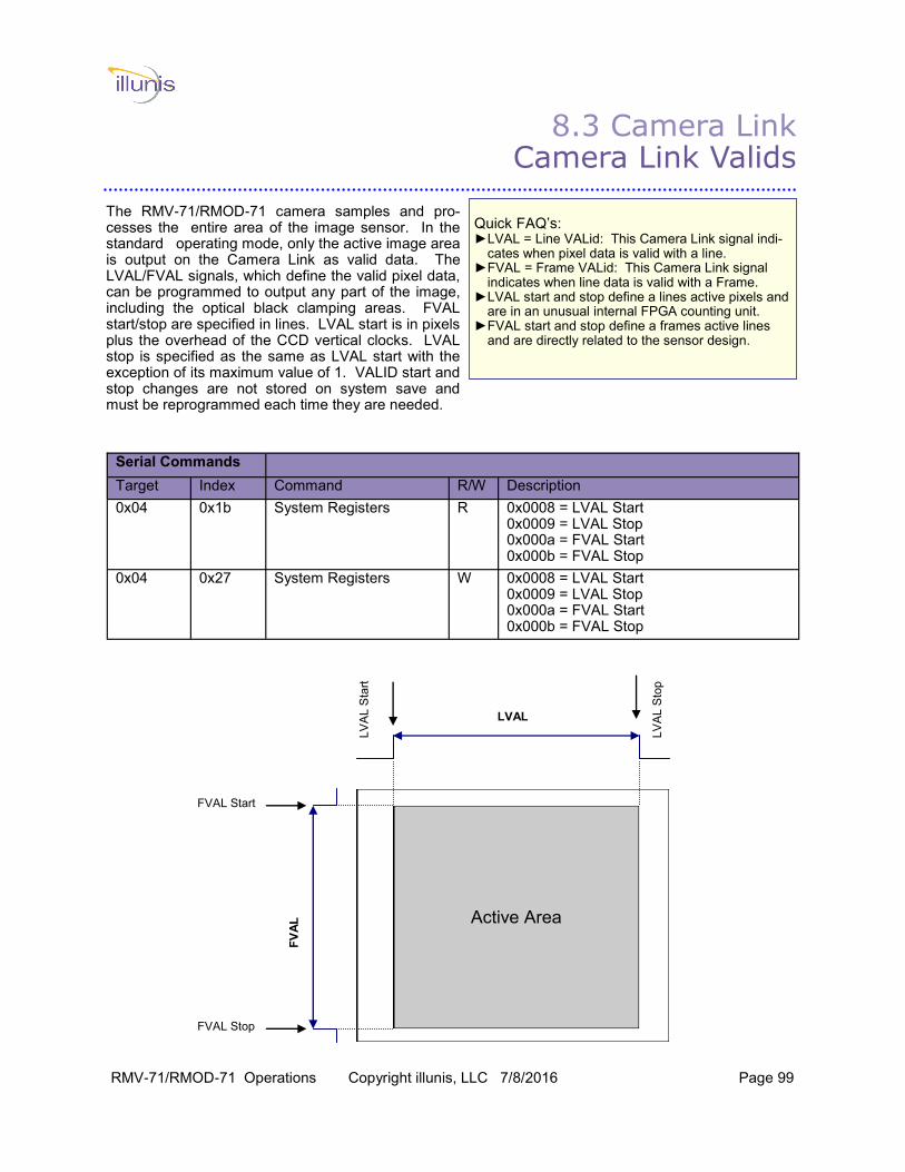
RMV-71/RMOD-71 Operations Copyright illunis, LLC 7/8/2016 Page 99
8.3 Camera Link Camera Link Valids
The RMV-71/RMOD-71 camera samples and pro-cesses the entire area of the image sensor. In the standard operating mode, only the active image area is output on the Camera Link as valid data. The LVAL/FVAL signals, which define the valid pixel data, can be programmed to output any part of the image, including the optical black clamping areas. FVAL start/stop are specified in lines. LVAL start is in pixels plus the overhead of the CCD vertical clocks. LVAL stop is specified as the same as LVAL start with the exception of its maximum value of 1. VALID start and stop changes are not stored on system save and must be reprogrammed each time they are needed.
Serial Commands
Target Index Command R/W Description
0x04 0x1b System Registers R 0x0008 = LVAL Start 0x0009 = LVAL Stop 0x000a = FVAL Start 0x000b = FVAL Stop
0x04 0x27 System Registers W 0x0008 = LVAL Start 0x0009 = LVAL Stop 0x000a = FVAL Start 0x000b = FVAL Stop
Quick FAQ’s: ►LVAL = Line VALid: This Camera Link signal indi-
cates when pixel data is valid with a line. ►FVAL = Frame VALid: This Camera Link signal
indicates when line data is valid with a Frame. ►LVAL start and stop define a lines active pixels and
are in an unusual internal FPGA counting unit. ►FVAL start and stop define a frames active lines
and are directly related to the sensor design.
Active Area
LV
AL S
tart
FV
AL
LVAL
LV
AL S
top
FVAL Start
FVAL Stop

RMV-71/RMOD-71 Operations Copyright illunis, LLC 7/8/2016 Page 100
8.4 Camera Link Raster and Exposure Detectors
Cameras similar to the RMV-71/RMOD-71 are very complex and can generate many different raster formats. To document all possible combinations of binning, partial scan, and triggering is next to im-possible; therefore, to alleviate this problem the RMV-71/RMOD-71 incorporates a set of Raster Detectors that measure the video image raster as sent to the capture device. These measured val-ues can be used to set the capture parameters. In addition to the raster size, an Exposure Detector is included. The Exposure Detector measures the exposure of the CCD sensor in units of the master pixel clock rate. The frame CRC is used in the Built In test functions of the camera.
Serial Commands
Target Index Command R/W Description
0x04 0x1b System Registers R 0x0000 = Pixels per line 0x0001 = Active pixels per line 0x0002 = Lines per frame 0x0003 = Active lines per frame 0x0012 = Exposure counter low word 0x0013 = Exposure counter high word 0x0014 = Frame CRC
Quick FAQ’s: ►Active pixels per line = LVAL active pixel count. ►Active lines per frame = FVAL active line count. ►The Exposure Detector counter is a 32 bit integer.
This gives a range of exposure from one clock peri-od to over 2 seconds.
►Exposure is measured in pixel clock periods. A 40Mhz clock has 0.025us periods. A 30Mhz clock has 0.033us periods. A 20Mhz clock has 0.050us periods.
Active Area
LV
AL S
tart
Ac
tive l
ine
s p
er
fram
e
Active pixels per line
LV
AL S
top
FVAL Start
FVAL Stop
Pixels per line
Lin
es p
er
fram
e
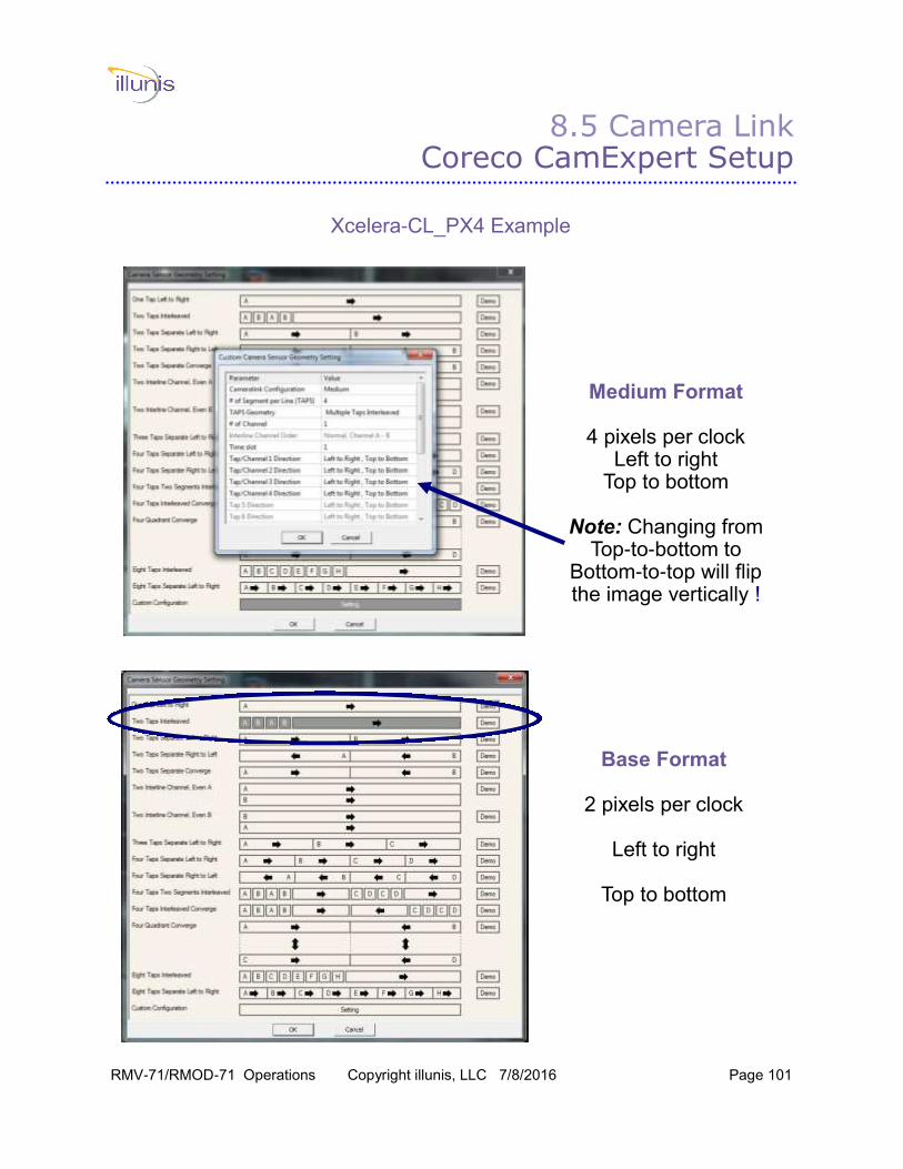
RMV-71/RMOD-71 Operations Copyright illunis, LLC 7/8/2016 Page 101
8.5 Camera Link Coreco CamExpert Setup
Xcelera-CL_PX4 Example
Medium Format
4 pixels per clock Left to right
Top to bottom
Note: Changing from Top-to-bottom to
Bottom-to-top will flip the image vertically !
Base Format
2 pixels per clock
Left to right
Top to bottom
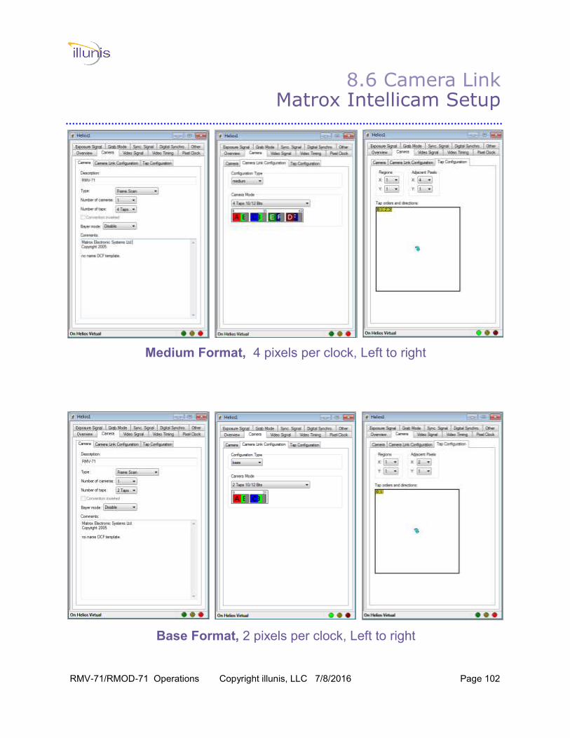
RMV-71/RMOD-71 Operations Copyright illunis, LLC 7/8/2016 Page 102
8.6 Camera Link Matrox Intellicam Setup
Base Format, 2 pixels per clock, Left to right
Medium Format, 4 pixels per clock, Left to right
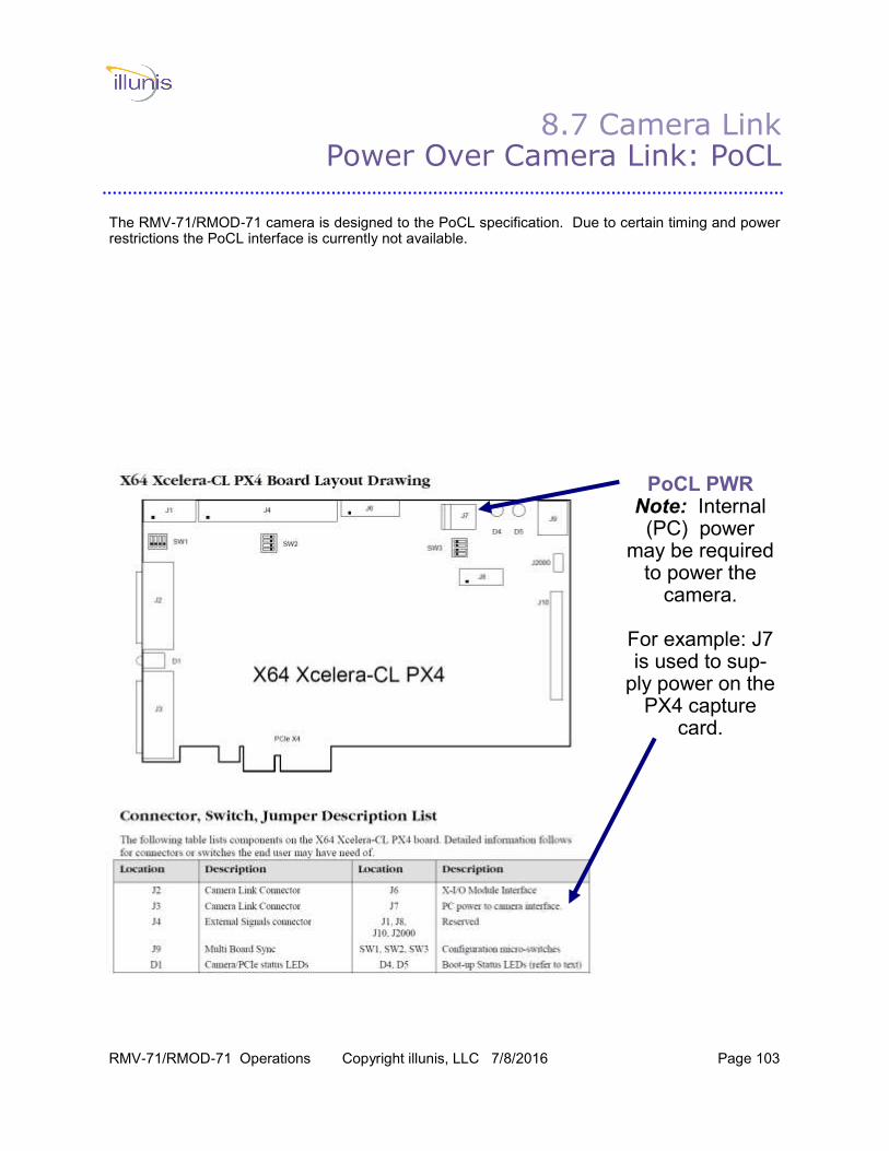
RMV-71/RMOD-71 Operations Copyright illunis, LLC 7/8/2016 Page 103
8.7 Camera Link Power Over Camera Link: PoCL
The RMV-71/RMOD-71 camera is designed to the PoCL specification. Due to certain timing and power restrictions the PoCL interface is currently not available.
PoCL PWR Note: Internal (PC) power
may be required to power the
camera.
For example: J7 is used to sup-
ply power on the PX4 capture
card.
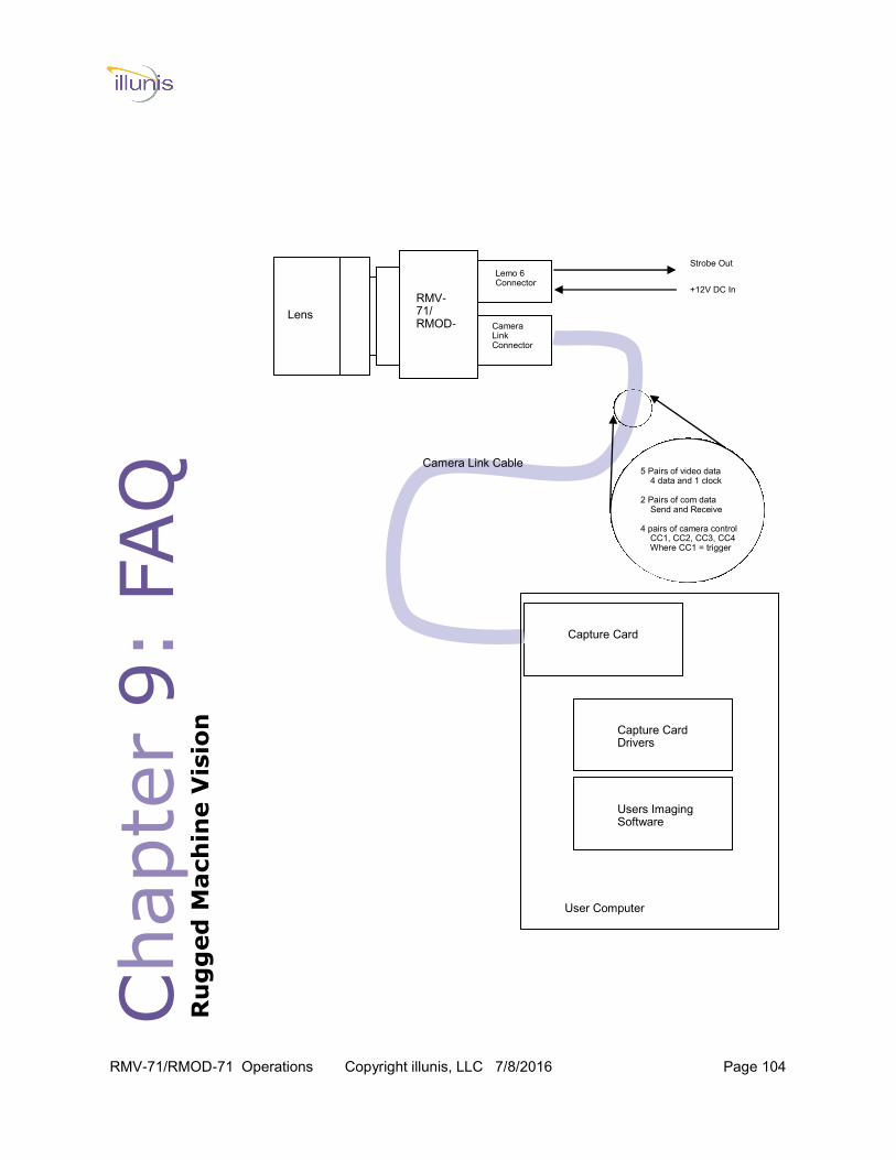
RMV-71/RMOD-71 Operations Copyright illunis, LLC 7/8/2016 Page 104
Chapte
r 9:
FAQ
Ru
gg
ed
Mach
ine V
isio
n
RMV-71/RMOD-
Capture Card
Lemo 6 Connector
Strobe Out
+12V DC In
Camera Link Connector
5 Pairs of video data 4 data and 1 clock 2 Pairs of com data Send and Receive 4 pairs of camera control CC1, CC2, CC3, CC4 Where CC1 = trigger
Lens
User Computer
Camera Link Cable
Capture Card Drivers
Users Imaging Software
RMV-71/RMOD-71 Operations Copyright illunis, LLC 7/8/2016 Page 105
FAQ
Ru
gg
ed
Mach
ine V
isio
n
This section of Frequently Asked Questions is intended to help the first time user to setup and control the RMV-71/RMOD-71 camera.
FAQ# 1: Coming soon !

RMV-71/RMOD-71 Operations Copyright illunis, LLC 7/8/2016 Page 106
IMPORTANT NOTICE:
illunis, LLC reserves the right to make changes to their products or to discontinue any prod-uct or service without notice. Before placing an order, illunis advises customers to obtain the latest version of relevant information to verify that information relied on is current. All products are sold subject to the illunis terms and conditions of sale supplied at the time of order acknowledgement, which includes those pertaining to warranty, patent infringement, and limitation of liability. illunis, LLC warrants performance of its products to the specifications applicable at the time of sale in accordance with the illunis standard warranty. Testing and other quality control techniques are utilized to the extent illunis deems necessary to support the warranty. Spe-cific testing of all parameters of each device is not necessarily performed, except those mandated by government requirements. In order to minimize risks associated with customer applications, adequate design and op-erating safeguards must be used by the customer to minimize inherent or procedural haz-ards. illunis products are not authorized for use as critical components in life support de-vices or systems that are intended for surgical implant into the body or to support or sustain life. Failure to perform when properly used in accordance with instructions for use provid-ed, can be reasonably expected to result in a significant injury to the user. A critical com-ponent can be defined as any component of a life support device or system whose failure to perform can be reasonably expected to cause the failure of the life support device or system, or to effect its safety or effectiveness. illunis assumes no liability for applications assistance or customer product design. illunis does not warrant or represent that any license, either express or implied, is granted under any patent, right, copyright, mask work right, or other intellectual property right of illunis covering or relating to any combination, machine, or process in which such products or services might be or are used. The illunis publication of information regarding any third party products or services does not constitute illunis approval, license, warranty, or en-dorsement thereof.
Reproduction of information from the illunis website or data sheets is permissible only if reproduction is without alteration and is accompanied by all associated warranties, condi-tions, limitations, and notices. Representation or reproduction of this information with alter-cation voids all warranties provided for an associated illunis product or service; it is an un-fair and deceptive business practice, and illunis is not responsible or liable for any such use.
For more information on any illunis products including detailed specifications and options please visit our web page at www.illunis.com or email [email protected] or call us at the number listed below. illunis specializes in applying our proven intellectual property to your custom requirements at realistic NRE fees - call and find your solution today.
illunis, LLC Phone: 952.975.9203 Worldwide Sales FAX: 952.294.8308 14700 Excelsior Blvd. email: [email protected] Minnetonka, MN 55345 web: www.illunis.com
Rugged M
achin
e V
isio
n
Ad
van
ced
Dig
ital M
ach
ine V
isio
n C
am
eras