Operational Amplifiers Selection Guide · 6 | Operational Amplifier Selection Guide JFET Input...
58
| 1 www.analog.com/opamps Operational Amplifiers Selection Guide 2011–2012 www.analog.com/opamps
Transcript of Operational Amplifiers Selection Guide · 6 | Operational Amplifier Selection Guide JFET Input...

| 1www.analog.com/opamps
Operational Amplifiers Selection Guide2011–2012
www.analog.com/opamps

2 | Operational Amplifier Selection Guide

| 3www.analog.com/opamps
Analog Devices Provides Amplifiers for Every Application
Why are there so many different types of operational amplifiers (op amps)? Here at Analog Devices our engineers continue the pursuit of the illusive ideal op amp. And while we’re extremely close to its realization, unfortunately it still exists only in textbooks. That is why we are committed to offering such a broad portfolio of op amps to meet the many and varied needs of our customers.
Selecting an op amp is no trivial task: with so many different types of amplifiers, categories, architectures, and parameters to choose from, the process can be difficult. Each customer and application requires slightly different performance. It doesn’t matter whether you’re designing a coffee
maker (yes, op amps can be found in coffee makers) or the next generation medical imaging system, Analog Devices has the right amplifier to meet your needs.
This document will help you quickly and easily identify the right op amp(s) for your application. Inside you’ll find a list of op amp terminology and processes used to fabricate the ICs, a variety of selection tables, application guides, design tools, and a handy detachable op amp reference wall chart. We hope you’ll refer to this selection guide often and that it provides you with a better understanding and appreciation of op amps and their many applications.
Contents
Op Amp Glossary . . . . . . . . . . . . . . . . . . . . . . . . . . . . . . . . . . . . . . . . . . . . . . . . . . . . . 4
Amplifier Design Technology . . . . . . . . . . . . . . . . . . . . . . . . . . . . . . . . . . . . . . . . . 5
Amplifier Process and Trimming Technology . . . . . . . . . . . . . . . . . . . . . . . . . 6
Quick Selection Guide—High Speed Amplifiers . . . . . . . . . . . . . . . . . . . . 7–8
Quick Selection Guide—Precision Amplifiers . . . . . . . . . . . . . . . . . . . . . 9–11
Amplifier Selection Guide by Specifications
Precision Amplifiers (BW < 50 MHz)
Zero-Drift . . . . . . . . . . . . . . . . . . . . . . . . . . . . . . . . . . . . . . . . . . . . . . . . . . . . . . . . . . . . . 15
Zero Input Crossover Distortion (ZCO) . . . . . . . . . . . . . . . . . . . . . . . . . . . . . . . . . . 16
Overvoltage Protection (OVP) . . . . . . . . . . . . . . . . . . . . . . . . . . . . . . . . . . . . . . . . . . . 17
Ultralow Offset Voltage (VOS # 250 mV Max) . . . . . . . . . . . . . . . . . . . . . . . . 18–19
Low Offset Voltage (VOS # 1 mV) . . . . . . . . . . . . . . . . . . . . . . . . . . . . . . . . . . . . . . . 20
Low Power (IS /Amp# 1 mA) . . . . . . . . . . . . . . . . . . . . . . . . . . . . . . . . . . . . . . . 21–22
Low Noise (Vn # 10 nV/√Hz) . . . . . . . . . . . . . . . . . . . . . . . . . . . . . . . . . . . . . . . 23–24
Low Input Bias Current (IB # 50 pA) . . . . . . . . . . . . . . . . . . . . . . . . . . . . . . . . 25–26
Single Supply . . . . . . . . . . . . . . . . . . . . . . . . . . . . . . . . . . . . . . . . . . . . . . . . . . . . . 27–28
Rail-to-Rail Output . . . . . . . . . . . . . . . . . . . . . . . . . . . . . . . . . . . . . . . . . . . . . . . . 29–31
Rail-to-Rail Input/Output . . . . . . . . . . . . . . . . . . . . . . . . . . . . . . . . . . . . . . . . . . 32–33
Low Cost . . . . . . . . . . . . . . . . . . . . . . . . . . . . . . . . . . . . . . . . . . . . . . . . . . . . . . . . . 34–35
High Speed Amplifiers (BW > 50 MHz)
Differential . . . . . . . . . . . . . . . . . . . . . . . . . . . . . . . . . . . . . . . . . . . . . . . . . . . . . . . . . . . 36
Low Noise/Low Distortion . . . . . . . . . . . . . . . . . . . . . . . . . . . . . . . . . . . . . . . . . . . . . . 37
Low Cost . . . . . . . . . . . . . . . . . . . . . . . . . . . . . . . . . . . . . . . . . . . . . . . . . . . . . . . . . . . . . 38
Rail-to-Rail Input/Output . . . . . . . . . . . . . . . . . . . . . . . . . . . . . . . . . . . . . . . . . . . . . . . 39
FastFET (FET Input) . . . . . . . . . . . . . . . . . . . . . . . . . . . . . . . . . . . . . . . . . . . . . . . . . . . . 40
Current Feedback . . . . . . . . . . . . . . . . . . . . . . . . . . . . . . . . . . . . . . . . . . . . . . . . . . . . . 41
High Output Current . . . . . . . . . . . . . . . . . . . . . . . . . . . . . . . . . . . . . . . . . . . . . . . . . . . 42
High Supply Voltage . . . . . . . . . . . . . . . . . . . . . . . . . . . . . . . . . . . . . . . . . . . . . . . . . . . 43
Clamp . . . . . . . . . . . . . . . . . . . . . . . . . . . . . . . . . . . . . . . . . . . . . . . . . . . . . . . . . . . . . . . . 44
Amplifier Selection Guide by Applications
Energy . . . . . . . . . . . . . . . . . . . . . . . . . . . . . . . . . . . . . . . . . . . . . . . . . . . . . . . . . . . . . . . . 45
Process Control and Industrial Automation . . . . . . . . . . . . . . . . . . . . . . . . . . . . . . 46
Instrumentation and Measurement . . . . . . . . . . . . . . . . . . . . . . . . . . . . . . . . . . . . . 47
Motor and Power Control . . . . . . . . . . . . . . . . . . . . . . . . . . . . . . . . . . . . . . . . . . . . . . 48
Healthcare . . . . . . . . . . . . . . . . . . . . . . . . . . . . . . . . . . . . . . . . . . . . . . . . . . . . . . . . 49–50
Communications . . . . . . . . . . . . . . . . . . . . . . . . . . . . . . . . . . . . . . . . . . . . . . . . . . . . . . 51
Consumer Audio . . . . . . . . . . . . . . . . . . . . . . . . . . . . . . . . . . . . . . . . . . . . . . . . . . . . . 52
Automotive . . . . . . . . . . . . . . . . . . . . . . . . . . . . . . . . . . . . . . . . . . . . . . . . . . . . . . . . . . . 53
Defense and Aerospace . . . . . . . . . . . . . . . . . . . . . . . . . . . . . . . . . . . . . . . . . . . .54–57
Tools, Evaluation Boards, and Other Design Resources . . . . . . . . . . .58–62
Design Equations—Commonly Used Amplifier Configurations . . . . .63–68
Packaging . . . . . . . . . . . . . . . . . . . . . . . . . . . . . . . . . . . . . . . . . . . . . . . . . . . . . . . .69–70

4 | Operational Amplifier Selection Guide
Op Amp Glossary
Common-Mode Voltage Range (CMVR) Also known as input voltage range, CMVR is the allowable input voltage range at both inputs before clipping or excessive nonlinearity is seen at the output.
Common-Mode Rejection Ratio (CMRR) The ratio of the common-mode voltage range (CMVR) to the change in the input offset voltage (ΔVoOS) over this range. The result is expressed in dB. CMRR (dB) = 20log (CMVR/ΔVOS)
Full Power Bandwidth The maximum frequency measured at unity gain for which the rated output voltage can be obtained for a sinusoidal signal at rated load without distortion due to slew rate limiting.
Gain Bandwidth Product (GBW) The product of open-loop gain and bandwidth at a specific frequency.
Input Bias Current (IB) The current at the input terminals.
Input Bias Current DriftThe proportional change in input bias current vs. temperature over a specified range of temperature.
Input Offset CurrentThe difference between the two input currents.
Input Offset Current DriftThe ratio of input offset current change over a specified temperature range, with the output held a constant voltage.
Input Offset Voltage Drift (TCVOS) The ratio of change in input offset voltage to a change in temperature.
Offset Voltage (VOS) The differential voltage needed across the op amp input terminals to obtain zero output voltage. Offset voltage values range varies by process and design technology:
•Auto-Zero Op Amps: <1 µV
•Precision Op Amps: 50 µV to 500 µV
•Best Bipolar Op Amps: 10 µV to 25 µV
•Best JFET Iput Op Amps: 100 µV to 1000 µV
•Best Bipolar High Speed Op Amps: 100 µV to 2000 µV
•Untrimmed CMOS Op Amps: >2 mV
•DigiTrim® CMOS Op Amps: <100 µV to 1000 µV
Open- Loop Gain (AVO) The ratio of the output voltage to the input offset voltage between the two input pins. The result is expressed in dB. Gain is usually specified only at dc (AO), but for many applications, such as high speed amplifiers for video and RF, the frequency dependence of gain is also important. For this reason the open loop gain and phase response is published for each amplifier.
Operating Supply Voltage Range The supply voltage range that can be applied to an amplifier for which it operates within specifications. Many applications implement op amp circuits with balanced dual supplies, while other applications for energy conservation or other reasons, use single-supply. For example, battery power in automotive and marine equipment provides only a single polarity. Even line-powered equipment, such as computers, may have only a single-polarity built-in supply, furnishing +5 V or +12 V dc for the system, or often as low as 1.8 V, with newer applications going even lower.
Power Supply Rejection Ratio (PSRR)The ratio of the change in power supply voltage to the change in input offset voltage. The result is expressed in dB. PSRR = 20log (ΔVSY/ΔVOS)
Settling TimeThe amount of time required for an amplifier to settle to some predetermined level of accuracy or percentage of output voltage after the application of a step input.
Slew Rate The maximum rate of change of output voltage under large signal condition. The result is usually expressed in V/µs.
Supply Current The current required from the supply voltage to operate the amplifier with no load.
Small Signal Unity Gain Frequency The frequency at which the open-loop gain is unity or 0 dB. This applies only to signals under 200 mV. Due to slew rate limiting, it is not possible to obtain large output voltage swings at high frequencies.

| 5www.analog.com/opamps
Amplifier Design Technology
Clamp AmplifiersClamp amplifiers allow the designer to specify a high (VCH) and low (VCL) output clamp voltage so the output signal will clamp at the specified levels. Analog Devices’ unique CLAMPIN™ input clamp architecture offers significant improvement in clamp performance compared to traditional output clamping devices, minimizing clamp error and distortion in the clamp region.
Common-Mode Linearized Amplifiers Increasing the linear input range of the input stage optimizes operational amplifier large signal distortion. This can be accomplished through the use of architectures such as degenerated differential structures and class AB input stages, both of which increase noise and lower precision. An alternate method is to linearize using a common-mode structure whose noise is rejected by the inherent differential nature of the input stage while also maintaining such precision metrics as CMRR, PSRR, and VOS. Analog Devices has numerous new amplifiers that now feature this new technology and has patented the common-mode linearized input architecture.
Current Feedback AmplifiersCurrent feedback amplifiers are primarily used in applications that require very high speed operation, large slew rates, and low distortion. The fundamental concept is based on the fact that, in bipolar transistor circuits, currents can be switched faster than voltages, all other things being equal. Unlike voltage feedback amplifiers (VFB), CFB amplifiers do not have balanced inputs. Instead, the noninverting input is high impedance, and the inverting input is low impedance. The open-loop gain of the CFB is measured in units of V (transimpedance gain) rather than V/V as for VFB amplifiers. Also, the value of the feedback resistor plays a direct role in the CFB’s stability. Therefore, adhering to the recommended feedback resistor suggested in the data sheet is highly recommended.
Differential AmplifiersDifferential amplifiers allow the process of single-ended input to complementary differential outputs or differential inputs to differential outputs. These amplifiers feature two separate feedback loops to control the differential and common-mode output voltages. Analog Devices’ differential amplifiers are configured with a VOCM pin, which can be easily adjusted for setting output common-mode voltage. This provides a convenient solution when interfacing with analog-to-digital converters (ADCs). ADI also offers a series of differential receiver products that convert differential input signals to single-ended output.
Quad Core (H Bridge)Analog Devices has patented the quad core architecture, which supplies current on-demand to charge and discharge the internal dominant pole capacitor, while allowing the quiescent current to be small. This patented architecture enables amplifiers to provide high slew rates with low distortion at low supply currents.
Overvoltage Protection (OVP) AmplifiersAn OVP amplifier is the most robust solution to protect the amplifier and entire circuitry from outside the rail input voltages due to manufacturing shorts, power supply timing, or human error. OVP is able to protect real estate from various unexpected errors, which in turns save time and money. OVP amplifiers require no external circuitry to provide protection.
Zero-Drift AmplifiersZero-drift amplifiers dynamically correct the offset voltage to achieve nanovolt-level offsets and extremely low offset drifts due to time and temperature. The 1/f noise, seen as a dc error, is also removed. Zero-drift amplifiers provide many benefits to designers, as temperature drift and 1/f noise, always nuisances in the system, are otherwise very difficult to eliminate. In addition, zero-drift amplifiers have higher open-loop gain, power supply rejection, and common-mode rejection as compared to standard amplifiers; and their overall output error is less than that obtained by a standard precision amplifier in the same configuration.
Zero Input Crossover Distortion (ZCO) AmplifiersTraditional rail-to-rail input amplifiers have an input stage that comprises two differential pairs, a p-type and an n-type. During the transition of the input common-mode voltage from the lower to the higher supply voltage, one of the differential pairs turns off and the other turns on. This transition causes crossover distortion. Zero input crossover distortion (ZCO) amplifiers solve this problem by integrating an on-chip charge pump. The charge pump increases the internal supply voltage, thus providing more headroom to the input stage. This allows the input stage to handle a wider range of input voltages (rail to rail) without using a second differential pair. As a result, crossover distortion is avoided.
6 | Operational Amplifier Selection Guide
JFET Input Amplifiers
JFET input amplifiers have the advantage over bipolar devices by having an extremely high input impedance along with low noise performance, making them very useful in amplifier circuits using very small signals such as high source impedance sensors and photodiodes. A typical JFET has a voltage noise slightly larger than a BJT, but its current noise is significantly lower.
Trimming Technology
Laser Trim
When extremely fine adjustment is required, laser trimming is most effective. By controlling the path and speed of the laser beam, the resistor’s value can be adjusted to very precise values. Analog Devices pioneered the use of thin film resistors and laser trimming and uses this technology extensively in precision amplifiers, references, and converters.
Zener Zapping
With each zap removing a predefined resistance value, the nature of the trims is discrete. It is most cost-effective for fairly large geometry processes. Analog Devices pioneered the use of Zener-zap trimming and created the industry standard OP07 precision amplifier.
DigiTrim
Analog Devices’ DigiTrim™ is a patented in-package trimming process that delivers guaranteed high accuracy. This in-package process technology eliminates the need for laser trimming during manufacturing and minimizes the input offset of operational amplifiers.
Process Technology
Bipolar
Bipolar technology delivers the best overall performance amplifiers. It offers high output current drive, high voltage operation, and low noise.
Extremely Fast Complementary Bipolar (XFCB 1.5)
Analog Device’s XFCB 1.5 technology is a suite of advanced bipolar fabrication processes that features dielectric isolation, high speed complementary NPNs and PNPs with 3 GHz to 8 GHz frequency transition, precision capacitors, and low temperature-coefficient thin film resistors that can be trimmed at the wafer level. Dielectric isolation allows much tighter spacing between components and removes the possibility of latch-up. Nonlinear device-to-substrate capacitance that limits device speed and distortion performance is eliminated. XFCB1.5 has supply voltage options from 8 V to 26 V; this allows the selection of the fastest devices possible for the required input and output voltage ranges.
XFCB3
Analog Devices’ XFCB3 technology features full dielectric isolation, silicon-germanium hetero-junction NPNs with frequency transition up to 50 GHz and double-poly PNPs with frequency transition up to 18 GHz, precision capacitors, and low temperature coefficient thin film resistors. Minimum feature size is a factor of three less than XFCB1.5. This process family has enabled a new generation of high speed, ultralow distortion differential amplifiers and op amps.
36 V iPolar
Analog Devices’ iPolar™ 36 V precision bipolar process is highly optimized for linear circuits, yielding new levels of performance, size, and value. The iPolar process combines the advantages of precision bipolar and JFET with lateral dielectric isolation and modular processing. The transistors on iPolar devices have been redesigned from the ground up and are optimized for speed, noise, matching, linearity, and stability at lower power levels. This enables greater signal chain integration without compromising performance.
16 V iCMOS Amplifiers
Analog Devices’ iCMOS® industrial manufacturing process technology combines submicron CMOS with high voltage complementary bipolar technologies. It enables the development of a wide range of high performance analog ICs capable of 30 V operation in a smaller footprint. Unlike analog ICs using conventional CMOS processes, iCMOS components can tolerate high supply voltages, while providing increased performance, dramatically lower power consumption, and reduced package size. iCMOS components tolerate high voltages (greater than 6 V regular CMOS amps) while employing digital design techniques such as auto-zero and DigiTrim technologies.
Amplifier Process and Trimming Technology

| 7www.analog.com/opamps
Quick Selection Guide for High Speed Operational Amplifiers (BW > 50 MHz) High Speed Op Amps
Low Noise, Low Distortion
<1 nV <2 nV <3 nV <6 nV
AD8099 ADA4899-1 ADA4841-1 AD8048
ADA4898-1 ADA4841-2 AD8047
ADA4898-2
ADA4896-2
ADA4897-1
ADA4897-2
AD8021
AD8022 (Dual)
ADA4857-1
ADA4857-2
AD8045
Rail-To-Rail
Rail-to-Rail In/Out (2.7 V to 10 V)
Single Dual Quad
Single Dual QuadTriple
Single Dual
Single Dual
QuadTriple
AD8031 AD8032
AD8027 AD8028
AD8029 AD8030 AD8040
Rail-to-Rail Out (3 V to 10 V)
ADA4853-1 ADA4853-2 ADA4853-3
ADA4850-1 ADA4850-2 ADA4855-3
AD8091 AD8092 ADA4856-3
AD8051 AD8052 AD8054
AD8041 AD8042 AD8044
Low Cost (<$1/Channel)
ADA4851-1 AD4851-2 ADA4851-4
AD8038 AD8039
AD8061 AD8062
AD8063
AD8055 AD8056
AD8057 AD8058
ADA4891-1 ADA4891-2 ADA4891-3 ADA4891-4
FastFET
ADA4817-1 ADA4817-2
AD8033 AD8034
AD8065 AD8066
AD8067
*G = 1
Single Dual QuadTriple
Triple
Single Dual Triple
Current Feedback (5 V to 10 V)
Low Cost (<$1/Channel)
ADA4860-1 ADA4861-3
AD8014 ADA4862-3
AD8072 AD8073
High Performance
AD8000 AD8002* AD8003 AD8004
AD8001* AD8008 AD8013
AD8005 AD8017 AD8023
AD8007 ADA4310-1
AD8009
AD8011*10 V only.
With Charge Pump
ADA4858-3
ADA4859-3
Single
High Supply Voltage ( 15 V)
ADA4898-1
AD818
Dual
AD828
AD847
AD817
AD827
AD826
AD829
AD844*
Single
High Current Output (>300 mA)
AD8390 AD8397
Dual
AD8392
Quad
Single
Fixed Gain (G = 2)
AD8079
Single
Adjustable Clamp Amplifiers
AD8036
AD8037
AD8075
ADA4862-3
ADA4856-3
ADA4859-3
ADA8074*
Triple
*±18 V
Single
Single Dual
Differential Amplifiers
ADA4927-1
ADA4930-1
ADA4932-1
ADA4927-2
ADA4930-2
ADA4932-2
ADA4937-1
ADA4938-1
ADA4939-1
ADA4937-2
ADA4938-2
ADA4939-2
ADA4940-2
ADA4950-2ADA4950-1
ADA4940-1
Differential Amplifier Receivers
AD8129
AD8130
ADA4922-1
ADA4941-1
ADA4960-1
AD8131
AD8137
AD8138
AD8139
AD8132
ADA4898-2

| 15www.analog.com/opamps
Zero Drift Amplifiers
ProcessPart
NumberNo. of Amps
Supply Voltage
(Min/Max)Rail-to-Rail1
BW @ ACL Min
(MHz)
Slew Rate
(V/ms)
VOS Max
(mV)TcVOS
(mv/°C Typ)
CMRR Min (dB)
PSRR Min (dB)
AVO Min (dB)
Noise (nV/√Hz) @ 1 kHz
IS/Amp
(mA Max)IB Max(pA)
PackagingPrice @ 1k
(OEM $US)
CMOSAD8628 AD8629 AD8630
1 2 4
2.7/6 RRIO 2.5 1 0.005 0.002 120 115 125 22 0.850 100SOT-23/SOIC MSOP/SOIC SOIC/TSSOP
0.96 1.47 2.73
CMOSADA4528-1 ADA4528-2*
12
2.2/5.5 RRIO 4 0.4 0.0025 0.015 115 120 130 5.3 1.500 100 MSOP/LFCSP1.15 1.90
CMOSADA4051-1 ADA4051-2
1 2
1.8/5.5 RRIO 0.125 0.06 0.015 0.02 110 110 115 95 0.017 70SC70/SOT-23MSOP/LFCSP
0.93 1.47
CMOSAD8538 AD8539
1 2
2.7/5.5 RRIO 0.43 0.35 0.013 0.03 115 105 115 50 0.180 25SOT-23/SOIC MSOP/SOIC
0.90 1.31
CMOSAD8551 AD8552 AD8554
1 2 4
2.7/6 RRIO 1.5 0.4 0.005 0.005 120 120 125 42 0.975 50MSOP/SOIC SOIC/TSSOP SOIC/TSSOP
1.20 1.90 3.36
CMOSAD8571 AD8572 AD8574
1 2 4
2.7/6 RRIO 1.5 0.4 0.005 0.005 120 120 125 51 0.850 50MSOP/SOIC SOIC/TSSOP SOIC/TSSOP
1.11 1.78 3.40
CMOSAD8638 AD8639
1 2
5/16 SS 1.5 2 0.009 0.03 127 127 130 60 1.500 75SOT-23/SOIC
MSOP/SOIC/LFCSP1.27 2.19
Precision Amplifiers (VOS < 1 mV, Bandwidth < 50 MHz)
Zero-Drift Amplifiers ADA4528-1: Precision, Ultralow Noise, RRIO, Zero-Drift Op Amp
The ADA4528-1 is an ultralow noise, zero-drift operational amplifier featuring rail-to-rail input and output swing. With an offset voltage of 2.5 mV, offset voltage drift of 0.015 mV/°C, and noise of 97 nV p-p (0.1 Hz to 10 Hz, AV = +100), the device is well suited for applications in which error sources cannot be tolerated. With wide operating supply range of 2.2 V to 5.5 V, high gain and excellent CMRR and PSRR specifications, the ADA4528-1 is ideal for precision amplification of low level signals, such as position and pressure sensors, strain gages, and medical instrumentation.
Features
• Low offset: 2.5 mV maximum
•Low offset voltage drift: 0.015 mV/°C maximum
•Low noise
•5.6 nV/√Hz at f = 1 kHz, AV = +100
•97 nV p-p at f = 0.1 Hz to 10 Hz, AV = +100
•Open-loop voltage gain: 130 dB minimum
•CMRR: 135 dB minimum
•PSRR: 130 dB minimum
•Gain bandwidth product: 4 MHz
•Single-supply operation: 2.2 V to 5.5 V
•Dual-supply operation: ±1.1 V to ±2.75 V
•Rail-to-rail input and output
•Unity-gain stable
Application
•Thermocouple/thermopile
•Load cell and bridge transducer
•Precision instrumentation
•Electronic scales
•Medical instrumentation
•Handheld test equipment
Voltage noise density vs. frequency.
1
10
100
1 10 100 1k 10k
VO
LTA
GE
NO
ISE
DE
NS
ITY
(nV
/√H
z)
FREQUENCY (Hz)
AV = 1
VSY = 5VVCM = VSY/2
no 1/f noise
*Prerelease 1 RRIO: Rail-to-rail input/output, RRO: rail-to-rail output, SS: single supply (IVR includes –VSY).

16 | Operational Amplifier Selection Guide
Precision Amplifiers (VOS < 1 mV, Bandwidth < 50 MHz)
Zero Input Crossover Distortion (ZCO) Amplifiers ADA4505-2: 10 µA, Rail-to-Rail I/O, Zero Input Crossover Distortion Amplifier
The ADA4505-x family solves the crossover distortion problem by using an on-chip charge pump to power the input differential pair. The charge pump creates a supply voltage higher than the voltage of the battery, allowing the input stage to handle a wide range of input signal voltages without using a second differential pair. With this solution, the input voltage can vary from one supply extreme to the other with no distortion, thereby restoring the full common-mode dynamic range of the op amp.
Features
•PSRR: 100 dB minimum
•CMRR: 105 dB typical
•Very low supply current: 10 mA per amplifier maximum
•1.8 V to 5.5 V single-supply or 60.9 V to 62.5 V dual-supply operation
•Rail-to-rail input/output
•3 mV offset voltage maximum
•Very low input bias current: 0.5 pA typical
Applications
•Pressure and position sensors
•Remote security
•Medical monitors
•Battery-powered consumer equipment
•Hazard detectors
Zero Input Crossover Distortion (ZCO) Amplifiers
ProcessPart
NumberNo. of Amps
Supply Voltage
(Min/Max)Rail-to-Rail1
BW @ ACL Min
(MHz)
Slew Rate
(V/ms)
VOS Max
(mV)TcVOS
(mv/°C Typ)
CMRR Min (dB)
PSRR Min (dB)
AVO Min (dB)
Noise (nV/√Hz) @ 1 kHz
IS/Amp
(mA Max)IB Max(pA)
PackagingPrice @ 1k
(OEM $US)
CMOSADA4505-12 ADA4505-2 ADA4505-4
1 2 4
1.8/5.5 RRIO 0.050 0.006 3 2 90 100 105 65 0.010 2 WLCSP/SOT-23 WLCSP/MSOP WLCSP/TSSOP
0.55 0.67 1.15
CMOSAD85052 AD8506 AD8508
1 2 4
1.8/5.5 RRIO 0.095 0.013 2.5 2 90 100 105 45 0.020 10 WLCSP/SOT-230.59 0.71 1.20
1 RRIO: rail-to-rail input/output, RRO: rail-to-rail output, SS: single supply (IVR includes –VSY).2 Check data sheet for test conditions and actual product specification—may be different for single/dual/quad amplifiers for part numbers with 2 mark.
Input offset voltage vs. common mode voltage.
140
120
100
80
60
40
20
00 1.0 1.50.5 2.0 2.5 3.0 3.5 4.54.0 5.0
VO
S (
V)
VCM (V)
TYPICALAMPLIFIER
ZCOAMPLIFIER
Circuit Note CN-0125, Precision Pulse Oximeter LED Current Sink Reference Circuit, www.analog.com/CN0125.
ADG1636
S1AD1
0.1F
10.3mA
CONNECT TORED LED CIRCUIT
D2
S1B
IN1
+5V
+5V+5V
22
1k
22pF
22pF
121 ±0.1%
10k
REDTIMING
S2A
S2B
IN2
EN GNDVSS
+5V
+5V
+1.25V
+5V
10k
53.6k
0.1F
10k
IRTIMING
ENABLE
ADR1581
1/2ADA4505-2
IRLMS2002
15.2mA
CONNECT TOINFRARED LED CIRCUIT
22
1k82.5 ±0.1%
1/2ADA4505-2
IRLMS2002
VDD

| 17www.analog.com/opamps
Precision Amplifiers (VOS < 1 mV, Bandwidth < 50 MHz)
Overvoltage Protection (OVP) Amplifiers ADA4091-2/ADA4091-4: Micropower, OVP, Rail-to-Rail Input/Output Operational Amplifier
The ADA4091-2 dual and ADA4091-4 quad are micropower, single-supply, 1.2 MHz bandwidth amplifiers featuring rail-to-rail inputs and outputs. They are guaranteed to operate from a +2.7 V to +30 V single supply, as well as from ±1.35 V to ±15 V dual supplies. The ADA4091 family features a unique input stage that allows the input voltage to exceed either supply safely without any phase reversal or latch-up; this is called overvoltage protection, or OVP.
Features
•Single-supply operation: 2.7 V to 36 V
•Rail-to-rail output swing
•Low supply current: 200 mA/amplifier
•Wide bandwidth: 1.2 MHz
•Low offset voltage: 250 mV maximum
•No phase reversal
•Overvoltage protection (OVP)
•25 V above/below supply rails at 65 V
•12 V above/below supply rails at 615 V
Applications
• Industrial process control
•Battery-powered instrumentation
•Power supply control and protection
•Telecommunications
•Remote sensors
•Low voltage strain gage amplifiers
•DAC output amplifiers
Overvoltage Protection (OVP) Amplifiers
ProcessPart
NumberNo. of Amps
Supply Voltage
(Min/Max)Rail-to-Rail1
BW @ ACL Min
(MHz)
Slew Rate
(V/ms)
VOS Max
(mV)TcVOS
(mv/°C Typ)
CMRR Min (dB)
PSRR Min (dB)
AVO Min (dB)
Noise (nV/√Hz) @ 1 kHz
IS/Amp
(mA Max)
OVP Level
(V)Packaging
Price @ 1k
(OEM $US)
BipolarOP191 OP291 OP491
1 2 4
2.7/12 RRIO 1.5 0.5 0.5 1.1 75 80 88 42 0.420101025
SOIC SOIC
SOIC/TSSOP/PDIP
1.69 2.22 3.60
BipolarADA4091-2 ADA4091-4
2 4
61.35/618 RRIO 1.27 0.46 0.25 2.5 104 108 116 25 0.250 12SOIC/LFCSP
LFCSP/TSSOP2.22 3.50
Bipolar ADA4092-4 4 61.35/618 RRIO 1.4 0.4 1.5 2.5 90 98 116 30 0.250 12 TSSOP 2.50
1 RRIO: rail-to-rail input/output, RRO: rail-to-rail output, SS: single supply (IVR includes –VSY).
Circuit Note CN-0111, Low Cost, High Voltage, Unipolar DAU Reference Circuit, www.analog.com/CN0111.
ADA4091-2
AD5292
ADR512
VDD
VSS
VDDV1
VOUTR1R2
12k
10nF
RBIASU1A
U1B
20k
1/2
ADA4091-22/2
+30V
+30V
VDD+30V
22.1k ± 1%1k ± 1%SERIAL
INTERFACE

18 | Operational Amplifier Selection Guide
Precision Amplifiers (Bandwidth < 50 MHz)
Ultralow Offset Voltage (VOS ≤ 250 µV Max) Amplifiers AD8597/AD8599: Ultralow Distortion, Ultralow Noise Operational Amplifier
The AD8597 (single) and AD8599 (dual) are very low noise, low distortion operational amplifiers ideal for use as preamplifiers. The low noise of 1.1 nV/√Hz and low harmonic distortion of −120 dB (or better) at audio bandwidths give the devices the wide dynamic range necessary for preamplifiers in audio, medical, and instrumentation applications. The excellent slew rate of 14 V/µs and 10 MHz gain bandwidth make them highly suitable for medical applications. The low distortion and fast settling time make them ideal for buffering of high resolution data converters.
Features
•Low noise: 1.1 nV/√Hz at 1 kHz
•Low distortion: –120 dB THD @ 1 kHz
•Bandwidth: 10 MHz
•Supply current: 4.8 mA/amp typical
•Low offset voltage: 10 µV typical
•CMRR: 120 dB
Applications
•Professional audio preamplifiers
•ATE/precision testers
• Imaging systems
•Medical/physiologic measurements
•Precision data conversion
Voltage noise density vs. frequency. AD8622: Dual, Low Power, Low Noise, Precision Amplifier
The AD8622 is a dual, precision, rail-to-rail output operational amplifier with a low supply current of only 350 µA maximum over temperature and supply voltage. It also offers ultralow offset, drift, and voltage noise combined with very low input bias current over the full operating temperature range. It is perfectly suited for applications where large error sources cannot be tolerated.
Features
•Very low offset voltage: 125 µA maximum
•Supply current: 215 µA/amp typical
• Input bias current: 200 pA maximum
•Low input offset voltage drift: 1.2 µV/°C maximum
•Very low voltage noise: 11 nV/√Hz
Applications
•Portable precision instrumentation
•Laser diode control loops
•Medical instrumentation
•Strain gage amplifier
•Thermocouple amplifiers
1 10 100 1k
100
1
0.1
FREQUENCY (Hz)
10
VO
LTA
GE
NO
ISE
DE
NS
ITY
(nV
/ H
z)
AD8599±5V ≤ VSY ≤ ±15V
1/2U1
R26.49k
C21.8F
R31k
R12.67k
C18.2F
+VSY
–VSY
+VSY
–VSY
SECTION A
1/2U1
R66.04k
C41.8F
R71kR4
9.09kR8
9.09k
R52.87k
C38.2F
SECTION B
U1 = AD8622
VIN
1/2U2
R1023.2k
C65.6F
R92.87k
C5680nF
SECTION C
1/2U2
R1229.4k
C810F
R114.75k
C7180nF
SECTION D
U2 = ADA4062-2
VOUT
+VSY
–VSY
+VSY
–VSY
V1
V2
V3
Circuit Note CN-0127, 8-Pole Active Low-Pass Filter Optimized for Precision, Low Noise, andHigh Gain Reference Circuit, www.analog.com/CN0127.

| 19www.analog.com/opamps
Circuit Note CN-0127, 8-Pole Active Low-Pass Filter Optimized for Precision, Low Noise, andHigh Gain Reference Circuit, www.analog.com/CN0127.
Ultralow Offset Voltage (VOS ≤ 250 µV Max) Amplifiers
ProcessPart
NumberNo. of Amps
Supply Voltage
(Min/Max)Rail-to-Rail1
BW @ ACL Min
(MHz)
Slew Rate
(V/ms)
VOS Max
(mV)
TcVOS (mv/°C
Typ)
CMRR Min (dB)
PSRR Min (dB)
AVO Min (dB)
Noise (nV/√Hz) @ 1 kHz
IS/Amp
(mA Max)IB Max Packaging
Price @ 1k
(OEM $US)
CMOSAD8628 AD8629 AD8630
1 2 4
2.7/6 RRIO 2.5 1 0.005 0.002 120 115 125 22 0.850 100 pASOT-23/SOIC MSOP/SOIC SOIC/TSSOP
0.96 1.47 2.73
CMOSAD8551 AD8552 AD8554
1 2 4
2.7/6 RRIO 1.5 0.4 0.005 0.005 120 120 125 42 0.975 50 pAMSOP/SOIC SOIC/TSSOP SOIC/TSSOP
1.20 1.90 3.36
CMOSAD8571 AD8572 AD8574
1 2 4
2.7/6 RRIO 1.5 0.4 0.005 0.005 120 120 125 51 0.850 50 pAMSOP/SOIC SOIC/TSSOP SOIC/TSSOP
1.11 1.78 3.40
CMOSAD8638 AD8639
1 2
5/16 SS 1.5 2 0.009 0.03 127 127 130 60 1.500 75 pASOT-23/SOIC
MSOP/SOIC/LFCSP1.18 1.86
CMOSADA4528-1 ADA4528-2*
12
2.2/5.5 RRIO 4 0.4 0.0025 0.015 115 120 130 5.3 1.500 100 pA MSOP/LFCSP1.15 1.90
CMOSAD8538 AD8539
1 2
2.7/5.5 RRIO 0.43 0.35 0.013 0.03 115 105 115 50 0.180 25 pASOT-23/SOIC MSOP/SOIC
0.90 1.31
CMOSADA4051-1 ADA4051-2
1 2
1.8/5.5 RRIO 0.125 0.06 0.015 0.02 110 110 115 95 0.017 70 pASC70/SOT-23 MSOP/LFCSP
0.93 1.47
Bipolar AD8676B 2 65/618 RRO 10 2.5 0.05 0.2 111 106 123 2.8 3.400 2 nA MSOP/SOIC 2.14
Bipolar AD8675 1 65/618 RRO 10 2.5 0.075 0.2 114 120 123 2.8 2.900 2 nA MSOP/SOIC 1.18
BipolarAD8671 AD8672 AD8674
1 2 4
65/618 10 4 0.075 0.3 100 110 120 2.8 3.500 12 nAMSOP/SOIC MSOP/SOIC SOIC/TSSOP
1.06 1.72 3.24
JFETAD8610B AD8620B
1 2 65/613 25 60 0.1 0.5 90 100 100 6 3.500 10 pA
MSOP/SOIC SOIC
9.86 16.70
Bipolar AD8676A 2 65/618 RRO 10 2.5 0.1 0.2 111 106 123 2.8 3.400 2 nA MSOP/SOIC 1.66
BipolarAD8597 AD8599
1 2 64.5/618 10 16.8 0.12 0.8 120 120 110 1.07 5.700 200 nA
SOIC/LFCSP SOIC
2.25 3.24
BipolarADA4004-1 ADA4004-2 ADA4004-4
1 2 4
65/618 12 2.7 0.125 0.7 110 110 114 1.8 2.200 90 nASOT-23/SOIC MSOP/SOIC SOIC/LFCSP
1.75 2.65 4.25
BipolarAD8622 AD8624
2 4 62.5/618 RRO 0.56 0.48 0.125 0.5 125 125 125 11 0.250 200 pA
MSOP/SOIC LFCSP/TSSOP
2.30 3.75
Bipolar AD8677 1 64/618 0.6 0.2 0.13 0.5 120 115 120 10 1.300 1 nA SOT-23/SOIC 0.76
CMOSAD8661 AD8662 AD8664
1 2 4
5/16 SS 4 3.5 0.16 4 90 95 106 12 1.550 1 pASOIC/LFCSP MSOP/SOIC SOIC/TSSOP
1.08 1.37 2.23
JFET ADA4627-1B 1 64/618 19 84 0.2 1 106 106 112 6.1 7.500 5 pA SOIC/LFCSP 10.75
CMOSAD8655 AD8656
1 2
2.7/5.5 RRIO 28 11 0.25 0.4 85 88 100 2.72 4.500 10 pAMSOP/SOIC MSOP/SOIC
0.71 1.11
JFETAD8610A AD8620A
1 2 65/613 25 60 0.25 0.8 90 100 100 6 3.500 10 pA
MSOP/SOIC SOIC
3.75 7.50
JFET AD549K 1 62.5/618 5 3 0.25 5 90 90 109 35 0.700 100 fA Header 19.11
BipolarADA4091-2 ADA4091-4
2 4 61.35/618 RRIO 1.27 0.46 0.25 2.5 104 108 116 25 0.250 55 nA
SOIC/LFCSP LFCSP/TSSOP
2.22 3.50
Bipolar-JFET
OP285 2 64.5/618 9 22 0.25 1 80 85 108 6 2.500 350 nA SOIC/PDIP 2.40
*Prerelease 1 RRIO: rail-to-rail input/output, RRO: rail-to-rail output, SS: single supply (IVR includes –VSY).
20 | Operational Amplifier Selection Guide
Precision Amplifiers (VOS < 1 mV, Bandwidth < 50 MHz)
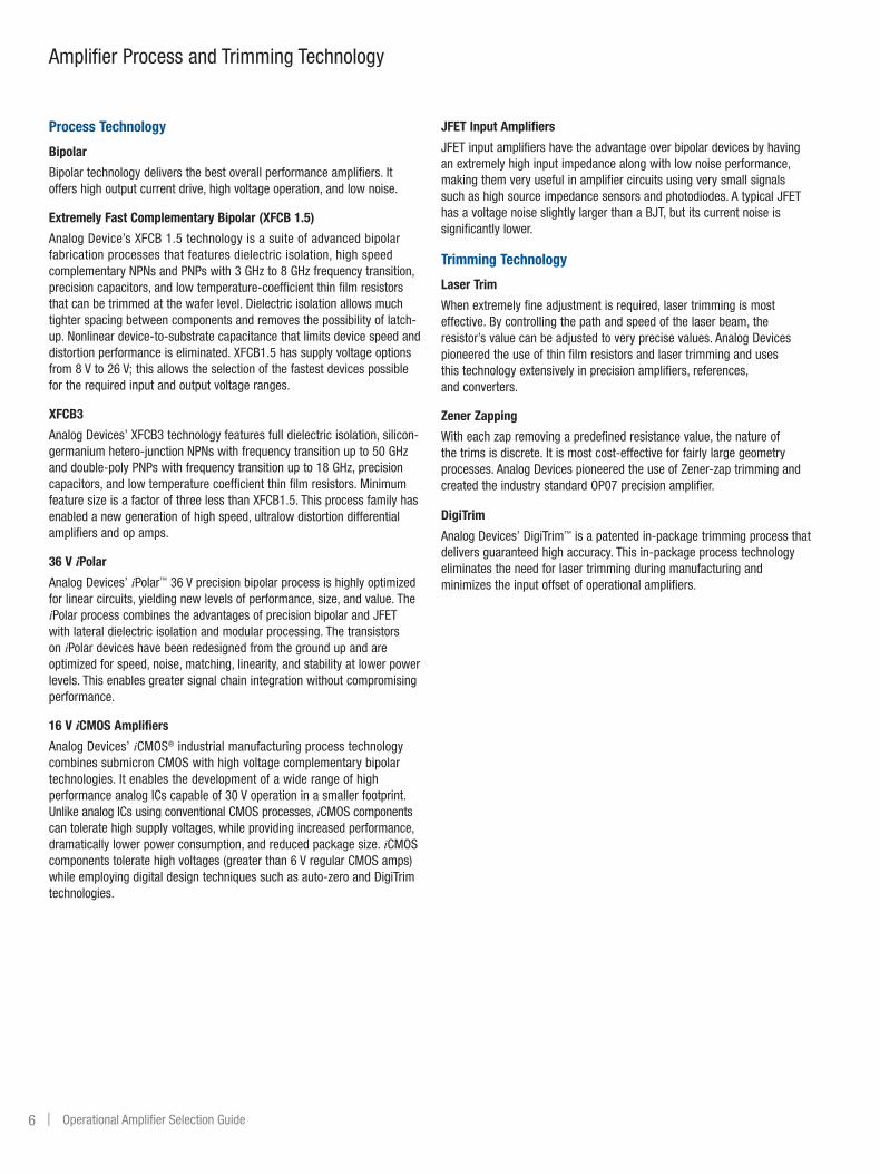
Low Offset Voltage (VOS ≤ 1 mV) AD8657: Precision, Micropower, 18 V CMOS RRIO Op Amplifier
The AD8657 is a dual, precision, micropower, rail-to-rail input/output (RRIO) amplifier optimized for low power and wide operating supply voltage range applications. The device operates from 2.7 V up to 18 V with a typical quiescent supply current of 18 mA and achieves low offset voltage thanks to Analog Devices’ patented DigiTrim trimming technique. The AD8657 also has high immunity to electromagnetic interference. The combination of low supply cur-rent, low offset voltage, very low input bias current, wide supply range, and rail-to-rail input and output makes the AD8657 ideal for current monitoring and current loops in process and motor control applications. In addition, the precision specifications make this device well suited for dc gain and buffering of sensor front ends or high impedance input sources in wireless or remote sensors or transmitters
Features
•Micropower at high voltage (18 V): 18 mA typical •Low offset voltage: 350 mV maximum •Single-supply operation: 2.7 V to 18 V •Dual-supply operation: ±1.35 V to ±9 V •Low input bias current: 20 pA •Gain bandwidth: 200 kHz •Unity-gain stable •Excellent electromagnetic interference immunity
Applications
•Portable operating systems •Current monitors •4 mA to 20 mA loop drivers •Buffer/level shifting •Multipole filters •Remote/wireless sensors •Low power transimpedance amplifiers
Low Offset Voltage (VOS ≤ 1mV) Amplifiers
ProcessPart
NumberNo. of Amps
Supply Voltage
(Min/Max)
VOS Max
(mV)TcVOS
(mv/°C Typ)Rail-to-Rail1
BW @ ACL Min
(MHz)
Slew Rate
(V/ms)
CMRR Min (dB)
PSRR Min (dB)
AVO Min (dB)
Noise (nV/√Hz) @ 1 kHz
IS/Amp
(mA Max)IB Max Packaging
Price @ 1k
(OEM $US)
CMOSAD8603 AD8607 AD8609
1 2 4
1.8/6 0.3 1 RRIO 0.4 0.1 85 80 112 25 0.040 1 pASOT-23
MSOP/SOIC SOIC/TSSOP
0.68 1.02 1.85
CMOSAD8605 AD8606 AD8608
1 2 4
2.7/6 0.3 1 RRIO 10 5 85 80 109 8 1.200 1 pAWLCSP/SOT-23
WLCSP/MSOP/SOIC SOIC/TSSOP
0.68 1.19 1.58
CMOSAD8663 AD8667 AD8669
1 2 4
5/16 0.3 1.5 SS 0.54 0.6 87 95 115 23 0.2850.3 pA
typ
SOIC/LFCSP MSOP/SOIC SOIC/TSSOP
1.17 1.58 2.70
CMOSAD8657 AD8659*
2 4
2.7/18 0.3 4 RRIO 0.175 0.3 95 105 110 50 0.022 5 pAMSOP/SOIC SOIC/LFCSP
0.95 1.35
JFET ADA4627-1A 1 64/618 0.3 1 19 84 100 103 106 6.1 7.500 5 pA SOIC/LFCSP 6.75
CMOSAD8651 AD8652
1 2
2.7/5.5 0.35 4 RRIO 50 41 80 76 100 4.52 14.000 10 pAMSOP/SOIC MSOP/SOIC
1.13 1.99
JFETAD8510B AD8512B
1 2 65/618 0.4 1 8 20 86 86 101 8 2.500 80 pA
MSOP/SOIC MSOP/SOIC
2.33 4.76
CMOSAD8601A AD8602A AD8604A
1 2 4
2.7/6 0.5 2 RRIO 8.2 5.2 74 67 89 33 1.200 60 pASOT-23
MSOP/SOIC SOIC/TSSOP
0.62 0.83 1.13
CMOSAD8615 AD8616 AD8618
1 2 4
2.7/6 0.5 1.5 RRIO 24 12 80 70 105 10 1.300 1 pASOT-23
MSOP/SOIC SOIC/TSSOP
0.76 1.29 2.29
JFETAD8627 AD8626 AD8625
1 2 4
65/613 0.75 2.5 SS 5 5 76 80 103 16 0.850 1 pASC70/SOIC MSOP/SOIC SOIC/TSSOP
1.60 2.63 4.09
JFETAD8641 AD8642 AD8643
1 2 4
62.5/613 0.75 2.5 SS 3.5 3 90 90 106 27.5 0.290 1 pASC70/SOIC MSOP/SOIC SOIC/LFCSP
1.47 2.35 3.85
Bipolar ADA4075-2 2 64.5/618 1 0.3 6.5 12 110 106 114 2.8 2.250 100 nA SOIC/LFCSP 0.75 CMOS AD8500 1 61.8/65.5 1 3 RRIO 0.007 0.004 75 90 98 190 0.001 10 pA SC70 0.71
JFETAD8510A AD8512A AD8513A
65/618 1 1.7 8 20 86 86 101 8 2.500 80 pAMSOP/SOIC MSOP/SOIC SOIC/TSSOP
0.951.493.71
JFETAD8682 AD8684
2 4 64.5/618 1 10 3.5 9 70 92 86 36 0.250 20 pA
MSOP/SOIC SOIC/TSSOP
1.66 2.44
*Prerelease 1 RRIO: rail-to-rail input/output, RRO: rail-to-rail output, SS: single supply (IVR includes –VSY).
4 mA to 20 mA current loop transmitter.
RL100Ω
VDD18V
C210F
C30.1F
C1390F
C40.1F
R43.3kΩ
Q1
D1 4mATO
20mA
R31.2kΩ
RNULL1MΩ
1%
VREF
RSPAN200kΩ
1%VIN0V TO 5V
R168kΩ
1%
R22kΩ1%
NOTES1. R1 + R2 = R´.
1/2AD8657
C510F
RSENSE100Ω
1%
VOUT
GND
ADR125VIN

| 21www.analog.com/opamps
Precision Amplifiers (VOS < 1 mV, Bandwidth < 50 MHz)
Low Power (IS/Amp ≤ 1 mA) Amplifiers AD8500: Micorpower, Precision CMOS Operational Amplifier
The AD8500 is a low power, precision CMOS op amp featuring a maximum supply current of 1 mA. The AD8500 has a maximum offset voltage of 1 mV and a typical input bias current of 1 pA, and it operates rail-to-rail on both the input and output. The AD8500 can operate from a single-supply voltage of +1.8 V to +5.5 V or a dual-supply voltage of 60.9 V to 62.75 V.
Features
•Supply current: 1 mA maximum
•Offset voltage: 1 mV maximum
•Single-supply or dual-supply operation
•Rail-to-rail input and output
•No phase reversal
•Unity-gain stable
Applications
•Portable equipment
•Remote sensors
•Low power filters
•Threshold detectors
AD623G = 10.06 AD8641
LEVEL SHIFTANTIALIAS
ESD DEFIB PROTECTION DEVICE
ANTIALIAS FILTER–3dB, 1592Hz
HIGH-PASS POLE0.05Hz
TOTAL GAIN ≈ 220
ADDITIONALDIGITAL FILTER
GAIN = 22.05
RAELECTRODE
LLELECTRODE
RLELECTRODE
5.23k 5.23k
+
108pF
AD8500
115k
499k
5pF
249k
681k
AGND
10k475
ADF702x*
MICRO-CONTROLLER
AD7466 OR AD7685*
+
4.7F
Low Power (IS/AMP ≤ 1mA) Amplifiers
ProcessPart
NumberNo. of Amps
Supply Voltage
(Min/Max)
IS/Amp
(mA Max)Rail-to-Rail1
BW @ ACL Min
(MHz)
Slew Rate
(V/ms)
VOS Max
(mV)
TcVOS (mv/°C
Typ)
CMRR Min (dB)
PSRR Min (dB)
AVO Min (dB)
Noise (nV/√Hz) @ 1 kHz
IB Max(pA)
PackagingPrice @ 1k
(OEM $US)
CMOS AD8500 1 1.8/5.5 0.001 RRIO 0.007 0.004 1 3 75 90 98 190 10 SC70 0.71
CMOSAD8502 AD8504
2 4
1.8/5.5 0.001 RRIO 0.007 0.004 3 5 67 85 98 190 10SOT-23 TSSOP
0.70 1.00
CMOSADA4505-1* ADA4505-2 ADA4505-4
1 2 4
1.8/5.5 0.010 RRIO 0.050 0.006 3 2 90 100 105 65 2 WLCSP/SOT-23 WLCSP/MSOP WLCSP/TSSOP
0.55 0.67 1.15
CMOSADA4051-1 ADA4051-2
1 2
1.8/5.5 0.017 RRIO 0.125 0.06 0.015 0.02 110 110 115 95 70SC70/SOT-23 MSOP/LFCSP
0.93 1.47
CMOSAD85052 AD8506 AD8508
1 2 4
1.8/5.5 0.020 RRIO 0.095 0.013 2.5 2 90 100 105 45 10WLCSP/SOT-23 WLCSP/MSOP WLCSP/TSSOP
0.59 0.71 1.20
CMOSAD8657 AD8659*
2 4
2.7/18 0.022 RRIO 0.175 0.3 0.3 4 95 105 110 50 5MSOP/SOIC SOIC/LFCSP
0.95 1.35
CMOSAD8603 AD8607 AD8609
1 2 4
1.8/6 0.040 RRIO 0.4 0.1 0.3 1 85 80 112 25 1SOT-23
MSOP/SOIC SOIC/TSSOP
0.68 1.02 1.85
CMOSAD8613 AD8617 AD8619
1 2 4
1.8/5.5 0.040 RRIO 0.4 0.1 2.2 1 68 67 107 25 1SC70/SOT-23 MSOP/SOIC SOIC/TSSOP
0.46 0.71 1.11
CMOSAD8541 AD8542 AD8544
1 2 4
2.7/6 0.045 RRIO 1 0.92 6 4 40 65 86 40 60SC70/SOT-23/SOIC MSOP/SOIC/TSSOP
SOIC/TSSOP
0.27 0.38 0.54
CMOSAD8538 AD8539
2 4
2.7/5.5 0.180 RRIO 0.43 0.35 0.013 0.03 115 105 115 50 25SOT-23/SOIC MSOP/SOIC
0.90 1.31
JFETADA4062-2A ADA4062-4A
2 4 64/618 0.220 1.4 3.3 2.5 4 73 74 76 36 50
MSOP/SOIC/LFCSP LFCSP/TSSOP
0.75 1.21
JFET ADA4062-2B 2 64/618 0.220 1.4 3.3 1.5 4 80 80 76 36 50 SOIC 1.25
CMOSADA4692-2 ADA4692-4
2 4
2.7/6 0.225 SS 3.6 1.3 2.5 1 75 80 95 16 5SOIC/LFCSP
TSSOP0.55 0.90
CMOSADA4691-2SD ADA4691-4SD
2 4
2.7/6 0.225 SS 3.6 1.3 2.5 1 75 80 95 16 5WLCSP/LFCSP
LFCSP0.57 0.99
JFETOP282 OP482
2 4 64.5/618 0.250 4 9 3 10 70 110 86 36 100
MSOP/SOIC SOIC/PDIP
1.31 2.06
*Prerelease
ECG signal chain using a micropower precision CMOS op amp.

22 | Operational Amplifier Selection Guide
Low Power (IS/Amp ≤ 1mA) Amplifiers (continued)
ProcessPart
NumberNo. of Amps
Supply Voltage
(Min/Max)
IS/Amp
(mA Max)Rail-to-Rail1
BW @ ACL Min
(MHz)
Slew Rate
(V/ms)
VOS Max
(mV)
TcVOS (mv/°C
Typ)
CMRR Min (dB)
PSRR Min (dB)
AVO Min (dB)
Noise (nV/√Hz) @ 1 kHz
IB Max PackagingPrice @ 1k
(OEM $US)
JFETAD8682 AD8684
2 4 64.5/618 0.250 3.5 9 1 10 70 92 86 36 20 pA
MSOP/SOIC SOIC/TSSOP
1.66 2.44
BipolarAD8622 AD8624
2 4 62.5/618 0.250 RRO 0.56 0.48 0.125 0.5 125 125 125 11 200 pA
MSOP/SOIC LFCSP/TSSOP
2.30 3.75
BipolarADA4091-2 ADA4091-4
2 4 61.35/618 0.250 RRIO 1.27 0.46 0.25 2.5 104 108 116 25 55 nA
SOIC/LFCSP LFCSP/TSSOP
2.22 3.50
BipolarADA4092-2* ADA4092-4
2 4 61.35/618 0.250 RRIO 1.4 0.4 1.5 2.5 90 98 116 30 60 nA
SOIC/LFCSP TSSOP
1.35 2.50
CMOSAD8663 AD8667 AD8669
1 2 4
5/16 0.285 SS 0.54 0.6 0.3 1.5 87 95 115 230.3 pA
typ
SOIC/LFCSP MSOP/SOIC SOIC/TSSOP
1.17 1.58 2.70
JFETAD8641 AD8642 AD8643
1 2 4
62.5/613 0.290 SS 3.5 3 0.75 2.5 90 90 106 27.5 1 pASC70/SOIC MSOP/SOIC SOIC/LFCSP
1.47 2.35 3.85
BP AD8631 1 1.8/6 RRIO SS 3 4 3.5 63 75 100 23 0.450 250 nA SOT-23 0.33
CMOS ADA4665-2 2 5/16 0.400 RRIO 1.2 1 6 3 55 70 85 32 1 pA MSOP/SOIC 0.70
CMOS AD8515 1 1.8 0.550 RRIO 5 2.7 6 4 60 65 113 22 30 pA SC70/SOT-23 0.28
JFET AD549J 1 62.5/618 0.700 5 3 1 20 80 80 109 35 250 fA TO-99 13.68
JFET AD549K 1 62.5/618 0.700 5 3 0.25 5 90 90 109 35 100 fA TO-99 19.11
JFET AD549L 1 62.5/618 0.700 5 3 0.5 10 90 90 109 35 60 fA TO-99 23.61
CMOSAD8591 SD AD8592 SD AD8594 SD
1 2 4
2.7/6 0.700 RRIO 3 5 25 20 38 45 83 45 50 pASOT-23
SOIC SOIC/TSSOP
0.29 0.39 0.57
CMOSAD8531 AD8532 AD8534
1 2 4
2.7/6 0.700 RRIO 3 5 25 20 38 45 83 45 50 pASC70/SOT-23
MSOP/SOIC/TSSOP SOIC/TSSOP
0.27 0.43 0.60
CBCMOSOP162 OP262 OP462
1 2 4
2.7/12 0.800 SS 15 13 0.325 1 70 60 97 9.5 500 nAMSOP/SOIC/TSSOP
SOIC/TSSOP SOIC/TSSOP
1.69 2.23 4.03
BipolarAD8565 AD8566 AD8567
1 2 4
4.5/16 0.850 RRIO 5 6 10 5 54 70 69 26 600 nASC70 MSOP
LFCSP/TSSOP
0.56 0.71 0.93
JFETAD8627 AD8626 AD8625
1 2 4
65/613 0.850 SS 5 5 0.75 2.5 76 80 103 16 1 pASC-70/SOIC MSOP/SOIC SOIC/TSSOP
1.60 2.63 4.09
CMOSAD8628 AD8629 AD8630
1 2 4
2.7/6 0.850 RRIO 2.5 1 0.005 0.002 120 115 125 22 100 pASOT-23/SOIC MSOP/SOIC SOIC/TSSOP
0.96 1.47 2.73
CMOSAD8571 AD8572 AD8574
1 2 4
2.7/6 0.850 RRIO 1.5 0.4 0.005 0.005 120 120 125 51 50 pAMSOP/SOIC SOIC/TSSOP SOIC/TSSOP
1.11 1.78 3.40
JFETAD820A AD822A AD824A
1 2 4
62.5/618 0.900 SS 1.9 3 2 2 70 70 114 16 25 pAMSOP/SOIC/PDIP MSOP/SOIC/PDIP
SOIC
1.82 2.76 4.55
JFETAD820B AD822B
1 2 62.5/618 0.900 SS 1.9 3 1 2 74 70 114 16 10 pA
SOIC/PDIP MSOP/SOIC/PDIP
2.66 4.11
CMOSAD8551 AD8552 AD8554
1 2 4
2.7/6 0.975 RRIO 1.5 0.4 0.005 0.005 120 120 125 42 50 pAMSOP/SOIC SOIC/TSSOP SOIC/TSSOP
1.20 1.90 3.36
*Prerelease 1 RRIO: rail-to-rail input/output, RRO: rail-to-rail output, SS: single supply (IVR includes –VSY).
| 23www.analog.com/opamps
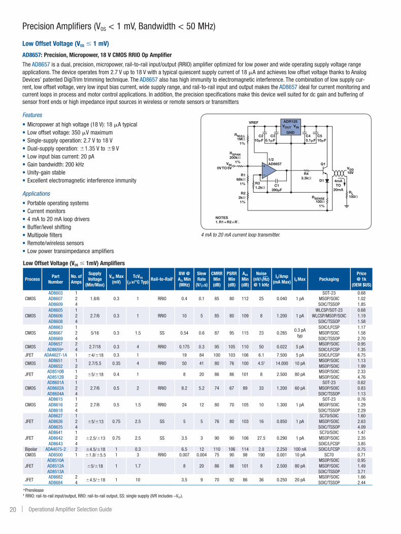
Balanced line driver design.
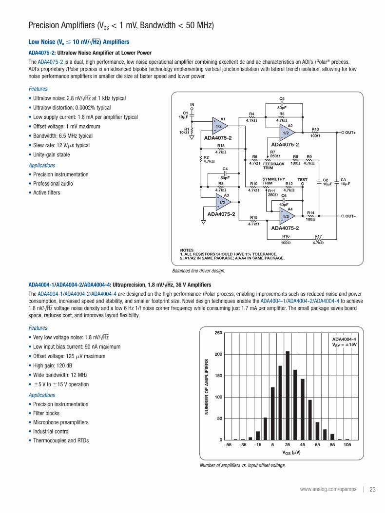
ADA4004-1/ADA4004-2/ADA4004-4: Ultraprecision, 1.8 nV/√Hz, 36 V Amplifiers
The ADA4004-1/ADA4004-2/ADA4004-4 are designed on the high performance iPolar process, enabling improvements such as reduced noise and power consumption, increased speed and stability, and smaller footprint size. Novel design techniques enable the ADA4004-1/ADA4004-2/ADA4004-4 to achieve 1.8 nV/√Hz voltage noise density and a low 6 Hz 1/f noise corner frequency while consuming just 1.7 mA per amplifier. The small package saves board space, reduces cost, and improves layout flexibility.
Features
•Very low voltage noise: 1.8 nV/√Hz
•Low input bias current: 90 nA maximum
•Offset voltage: 125 mV maximum
•High gain: 120 dB
•Wide bandwidth: 12 MHz
• 65 V to 615 V operation
Applications
•Precision instrumentation
•Filter blocks
•Microphone preamplifiers
• Industrial control
•Thermocouples and RTDs
Number of amplifiers vs. input offset voltage.
250
200
150
100
50
0–55 –35 –15 5 25 45 65 85 105
NU
MB
ER
OF
AM
PLI
FIE
RS
VOS (V)
ADA4004-4VSY = ±15V
C310F
R24.7k
OUT+
OUT–
1/2
ADA4075-2
R5
4.7k
R6
4.7k
R7250 R8
100
R9
4.7k
R13
100
R4
4.7kA21/2
ADA4075-2
A1
IN
C5
50pFC1
10F
C210F
TESTSYMMETRYTRIM
FEEDBACKTRIM
1/2
ADA4075-2
R12
4.7kR11250
R17
4.7k
R16
100
R10
4.7k
R15
4.7k
A4
C6
50pF1/2
ADA4075-2
A3
C4
50pF
R14
100
R110k
NOTES1. ALL RESISTORS SHOULD HAVE 1% TOLERANCE.2. A1/A2 IN SAME PACKAGE; A3/A4 IN SAME PACKAGE.
R3
4.7k
R18
4.7k
Precision Amplifiers (VOS < 1 mV, Bandwidth < 50 MHz)
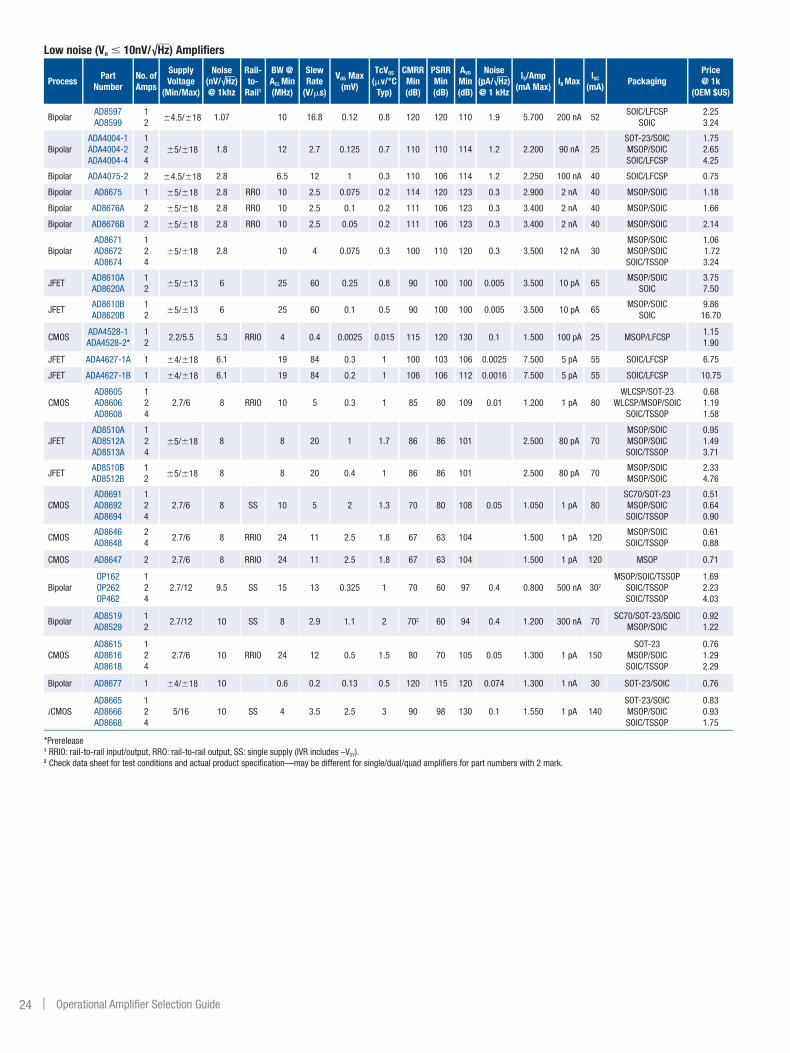
Low Noise (Vn ≤ 10 nV/√Hz) Amplifiers
ADA4075-2: Ultralow Noise Amplifier at Lower Power
The ADA4075-2 is a dual, high performance, low noise operational amplifier combining excellent dc and ac characteristics on ADI’s iPolar® process. ADI’s proprietary iPolar process is an advanced bipolar technology implementing vertical junction isolation with lateral trench isolation, allowing for low noise performance amplifiers in smaller die size at faster speed and lower power.
Features
•Ultralow noise: 2.8 nV/√Hz at 1 kHz typical
•Ultralow distortion: 0.0002% typical
•Low supply current: 1.8 mA per amplifier typical
•Offset voltage: 1 mV maximum
•Bandwidth: 6.5 MHz typical
•Slew rate: 12 V/ms typical
•Unity-gain stable
Applications
•Precision instrumentation
•Professional audio
•Active filters
24 | Operational Amplifier Selection Guide
Low noise (Vn ≤ 10nV/√Hz) Amplifiers
ProcessPart
NumberNo. of Amps
Supply Voltage
(Min/Max)
Noise (nV/√Hz) @ 1khz
Rail-to-
Rail1
BW @ ACL Min
(MHz)
Slew Rate
(V/ms)
VOS Max
(mV)
TcVOS (mv/°C
Typ)
CMRR Min (dB)
PSRR Min (dB)
AVO Min (dB)
Noise (pA/√Hz) @ 1 kHz
IS/Amp
(mA Max)IB Max
ISC
(mA)Packaging
Price @ 1k
(OEM $US)
BipolarAD8597 AD8599
1 2 64.5/618 1.07 10 16.8 0.12 0.8 120 120 110 1.9 5.700 200 nA 52
SOIC/LFCSP SOIC
2.25 3.24
BipolarADA4004-1 ADA4004-2 ADA4004-4
1 2 4
65/618 1.8 12 2.7 0.125 0.7 110 110 114 1.2 2.200 90 nA 25SOT-23/SOIC MSOP/SOIC SOIC/LFCSP
1.75 2.65 4.25
Bipolar ADA4075-2 2 64.5/618 2.8 6.5 12 1 0.3 110 106 114 1.2 2.250 100 nA 40 SOIC/LFCSP 0.75
Bipolar AD8675 1 65/618 2.8 RRO 10 2.5 0.075 0.2 114 120 123 0.3 2.900 2 nA 40 MSOP/SOIC 1.18
Bipolar AD8676A 2 65/618 2.8 RRO 10 2.5 0.1 0.2 111 106 123 0.3 3.400 2 nA 40 MSOP/SOIC 1.66
Bipolar AD8676B 2 65/618 2.8 RRO 10 2.5 0.05 0.2 111 106 123 0.3 3.400 2 nA 40 MSOP/SOIC 2.14
BipolarAD8671 AD8672 AD8674
1 2 4
65/618 2.8 10 4 0.075 0.3 100 110 120 0.3 3.500 12 nA 30MSOP/SOIC MSOP/SOIC SOIC/TSSOP
1.06 1.72 3.24
JFETAD8610A AD8620A
1 2 65/613 6 25 60 0.25 0.8 90 100 100 0.005 3.500 10 pA 65
MSOP/SOIC SOIC
3.75 7.50
JFETAD8610B AD8620B
1 2 65/613 6 25 60 0.1 0.5 90 100 100 0.005 3.500 10 pA 65
MSOP/SOIC SOIC
9.86 16.70
CMOSADA4528-1 ADA4528-2*
12
2.2/5.5 5.3 RRIO 4 0.4 0.0025 0.015 115 120 130 0.1 1.500 100 pA 25 MSOP/LFCSP1.151.90
JFET ADA4627-1A 1 64/618 6.1 19 84 0.3 1 100 103 106 0.0025 7.500 5 pA 55 SOIC/LFCSP 6.75
JFET ADA4627-1B 1 64/618 6.1 19 84 0.2 1 106 106 112 0.0016 7.500 5 pA 55 SOIC/LFCSP 10.75
CMOSAD8605 AD8606 AD8608
1 2 4
2.7/6 8 RRIO 10 5 0.3 1 85 80 109 0.01 1.200 1 pA 80WLCSP/SOT-23
WLCSP/MSOP/SOIC SOIC/TSSOP
0.68 1.19 1.58
JFETAD8510A AD8512A AD8513A
1 2 4
65/618 8 8 20 1 1.7 86 86 101 2.500 80 pA 70MSOP/SOIC MSOP/SOIC SOIC/TSSOP
0.95 1.49 3.71
JFETAD8510B AD8512B
1 2 65/618 8 8 20 0.4 1 86 86 101 2.500 80 pA 70
MSOP/SOIC MSOP/SOIC
2.33 4.76
CMOSAD8691 AD8692 AD8694
1 2 4
2.7/6 8 SS 10 5 2 1.3 70 80 108 0.05 1.050 1 pA 80SC70/SOT-23 MSOP/SOIC SOIC/TSSOP
0.51 0.64 0.90
CMOSAD8646 AD8648
2 4
2.7/6 8 RRIO 24 11 2.5 1.8 67 63 104 1.500 1 pA 120MSOP/SOIC SOIC/TSSOP
0.61 0.88
CMOS AD8647 2 2.7/6 8 RRIO 24 11 2.5 1.8 67 63 104 1.500 1 pA 120 MSOP 0.71
BipolarOP162 OP262 OP462
1 2 4
2.7/12 9.5 SS 15 13 0.325 1 70 60 97 0.4 0.800 500 nA 302
MSOP/SOIC/TSSOP SOIC/TSSOP SOIC/TSSOP
1.69 2.23 4.03
BipolarAD8519 AD8529
1 2
2.7/12 10 SS 8 2.9 1.1 2 702 60 94 0.4 1.200 300 nA 70SC70/SOT-23/SOIC
MSOP/SOIC0.92 1.22
CMOSAD8615 AD8616 AD8618
1 2 4
2.7/6 10 RRIO 24 12 0.5 1.5 80 70 105 0.05 1.300 1 pA 150SOT-23
MSOP/SOIC SOIC/TSSOP
0.76 1.29 2.29
Bipolar AD8677 1 64/618 10 0.6 0.2 0.13 0.5 120 115 120 0.074 1.300 1 nA 30 SOT-23/SOIC 0.76
iCMOSAD8665 AD8666 AD8668
1 2 4
5/16 10 SS 4 3.5 2.5 3 90 98 130 0.1 1.550 1 pA 140SOT-23/SOIC MSOP/SOIC SOIC/TSSOP
0.83 0.93 1.75
*Prerelease 1 RRIO: rail-to-rail input/output, RRO: rail-to-rail output, SS: single supply (IVR includes –VSY). 2 Check data sheet for test conditions and actual product specification—may be different for single/dual/quad amplifiers for part numbers with 2 mark.

| 25www.analog.com/opamps
Voted as one of the Hot 100 Electronic
Products of 2009, EDN Magazine
Precision Amplifiers (VOS < 1 mV, Bandwidth < 50 MHz)
Low Input Bias Current (IB ≤ 50 pA) Amplifiers ADA4627–1: Low Noise, Low Bias Current, JFET Operational Amplifier
The ADA4627–1 is a wide bandwidth precision amplifier featuring low noise, very low offset, drift, and bias current. Operation is specified from 65 V to 615 V dual supply. This amplifier combines the best specifications of precision dc and high speed ac op amps.
Features
•Low offset voltage: 200 mV maximum
•Offset drift: 1 mV/°C typical
•Very low input bias current: 5 pA maximum
•Extended temperature range: −40°C to +125°C
• 65 V to 615 V dual supply
•Guaranteed GBW: 16 MHz
•Voltage noise: 6.1 nV/√Hz at 1 kHz
•High slew rate: 60 V/ms
Applications
•High impedance sensors
•Photodiode amplifier
•Precision instrumentation
•Phase-locked loop filters
•High end professional audio
•Medical
Low Input Bias Current ( IB ≤ 50 pA) Amplifiers
ProcessPart
NumberNo. of Amps
Supply Voltage
(Min/Max)
Rail-to-
Rail1
BW @ ACL Min
(MHz)
Slew Rate
(V/ms)
VOS Max
(mV)
TcVOS (mv/°C
Typ)
CMRR Min (dB)
PSRR Min (dB)
AVO Min (dB)
Noise (nV/√Hz) @ 1 kHz
Noise (pA/√Hz) @ 1 kHz
IS/Amp
(mA Max)IB Max Packaging
Price @ 1k
(OEM $US)
JFET AD549L 1 62.5/618 5 3 0.5 10 90 90 109 35 0.22 0.700 60 fA TO-99 23.61
JFET AD549K 1 62.5/618 5 3 0.25 5 90 90 109 35 0.22 0.700 100 fA TO-99 19.11
JFET AD549J 1 62.5/618 5 3 1 20 80 80 109 35 0.22 0.700 250 fA TO-99 13.68
BiJET OP285 2 64.5/618 9 22 0.25 1 80 85 108 6 0.9 2.500 350 nA SOIC/PDIP 2.40
CMOSAD8663 AD8667 AD8669
1 2 4
5/16 SS 0.54 0.6 0.3 1.5 87 95 115 23 0.05 0.2850.3 pA
typ
SOIC/LFCSP MSOP/SOIC SOIC/TSSOP
1.17 1.58 2.70
CMOSAD8603 AD8607 AD8609
1 2 4
1.8/6 RRIO 0.4 0.1 0.3 1 85 80 112 25 0.05 0.040 1 pASOT-23
MSOP/SOIC SOIC/TSSOP
0.68 1.02 1.85
CMOSAD8605 AD8606 AD8608
1 2 4
2.7/6 RRIO 10 5 0.3 1 85 80 109 8 0.01 1.200 1 pAWLCSP/SOT-23
WLCSP/MSOP/SOIC SOIC/TSSOP
0.68 1.19 1.58
CMOSAD8615 AD8616 AD8618
1 2 4
2.7/6 RRIO 24 12 0.5 1.5 80 70 105 10 0.05 1.300 1 pASOT-23
MSOP/SOIC SOIC/TSSOP
0.76 1.29 2.29
CMOSAD8661 AD8662 AD8664
1 2 4
5/16 SS 4 3.5 0.16 4 90 95 106 12 0.1 1.550 1 pASOIC/LFCSP MSOP/SOIC SOIC/TSSOP
1.08 1.37 2.23
JFETAD8627 AD8626 AD8625
1 2 4
65/613 SS 5 5 0.75 2.5 76 80 103 16 0.5 0.850 1 pASC70/SOIC MSOP/SOIC SOIC/TSSOP
1.60 2.63 4.09
JFETAD8641 AD8642 AD8643
1 2 4
62.5/613 SS 3.5 3 0.75 2.5 90 90 106 27.5 0.0005 0.290 1 pASC70/SOIC MSOP/SOIC SOIC/LFCSP
1.47 2.35 3.85
CMOSAD8613 AD8617 AD8619
1 2 4
1.8/5.5 RRIO 0.4 0.1 2.2 1 68 67 107 25 0.05 0.040 1 pASC70/SOT-23 MSOP/SOIC SOIC/TSSOP
0.46 0.71 1.11
CMOSAD8691 AD8692 AD8694
1 2 4
2.7/6 SS 10 5 2 1.3 70 80 108 8 0.05 1.050 1 pASC70/SOT-23 MSOP/SOIC SOIC/TSSOP
0.51 0.64 0.90
Building an in-amp with gain = 201. Refer to Circuit Note CN-0122 for more information on this reference circuit at www.analog.com/cn0122.
–IN
+IN
10k
10k
10k
10k
ADA4627-1
ADA4627-1
RG20
RF1
RF2
2k
AD8271
OUT
2k
VS = ±15V
+VS
+VS
–VS
+VS
–VS
–VS
NOTES1. 10k THIN FILM TRIMMED RESISTOR
ARE INTERNAL TO THE AD8271.

26 | Operational Amplifier Selection Guide
Low Input Bias Current ( IB ≤ 50 pA) Amplifiers (continued)
ProcessPart
NumberNo. of Amps
Supply Voltage
(Min/Max)
Rail-to-
Rail1
BW @ ACL Min
(MHz)
Slew Rate
(V/ms)
VOS Max
(mV)
TcVOS (mv/°C
Typ)
CMRR Min (dB)
PSRR Min (dB)
AVO Min (dB)
Noise (nV/√Hz) @ 1 kHz
Noise (pA/√Hz) @ 1 kHz
IS/Amp
(mA Max)IB Max(pA)
PackagingPrice @ 1k
(OEM $US)
CMOSAD8646 AD8648
2 4
2.7/6 RRIO 24 11 2.5 1.8 67 63 104 8 1.500 1MSOP/SOIC SOIC/TSSOP
0.61 0.88
CMOS AD8647 2 2.7/6 RRIO 24 11 2.5 1.8 67 63 104 8 1.500 1 MSOP 0.71
CMOSAD8665 AD8666 AD8668
1 2 4
5/16 SS 4 3.5 2.5 3 90 98 130 10 0.1 1.550 1SOT-23/SOIC MSOP/SOIC SOIC/TSSOP
0.83 0.93 1.75
CMOS ADA4665-2 2 5/16 RRIO 1.2 1 6 3 55 70 85 32 0.400 1 MSOP/SOIC 0.70
CMOSADA4505-12 ADA4505-2 ADA4505-4
1 2 4
1.8/5.5 RRIO 0.050 0.006 3 2 90 100 105 65 0.02 0.010 2WLCSP/SOT-23 WLCSP/MSOP WLCSP/TSSOP
0.55 0.67 1.15
CMOSAD8657 AD8659*
2 4
2.7/18 RRIO 0.175 0.3 0.3 4 95 105 110 50 0.022 5MSOP/SOIC SOIC/LFCSP
0.951.35
JFET ADA4627-1A 1 64/618 19 84 0.3 1 100 103 106 6.1 0.0025 7.500 5 SOIC/LFCSP 6.75
JFET ADA4627-1B 1 64/618 19 84 0.2 1 106 106 112 6.1 0.0016 7.500 5 SOIC/LFCSP 10.75
CMOSADA4692-2 ADA4692-4
2 4
2.7/6 SS 3.6 1.3 2.5 1 75 80 95 16 0.05 0.225 5SOIC/LFCSP
TSSOP0.55 0.90
CMOSADA4691-2 ADA4691-4
2 4
2.7/6 SS 3.6 1.3 2.5 1 75 80 95 16 0.05 0.225 5WLCSP/LFCSP
LFCSP0.57 0.99
CMOS AD8500 1 1.8/5.5 RRIO 0.007 0.004 1 3 75 90 98 190 0.1 0.001 10 SC70 0.71
CMOSAD8655 AD8656
1 2
2.7/5.5 RRIO 28 11 0.25 0.4 85 88 100 2.72 4.500 10MSOP/SOIC MSOP/SOIC
0.71 1.11
CMOSAD8651 AD8652
1 2
2.7/5.5 RRIO 50 41 0.35 4 80 76 100 4.52 0.025 14.000 10MSOP/SOIC MSOP/SOIC
1.13 1.99
JFETAD8610A AD8620A
1 2 65/613 25 60 0.25 0.8 90 100 100 6 0.005 3.500 10
MSOP/SOIC SOIC
3.75 7.50
JFETAD8610B AD8620B
1 2 65/613 25 60 0.1 0.5 90 100 100 6 0.005 3.500 10
MSOP/SOIC SOIC
9.86 16.70
JFETAD820B AD822B
1 2 62.5/618 SS 1.9 3 1 2 74 70 114 16 0.008 0.900 10
SOIC/PDIP MSOP/SOIC/PDIP
2.66 4.11
CMOSAD85052 AD8506 AD8508
1 2 4
1.8/5.5 RRIO 0.095 0.013 2.5 2 90 100 105 45 0.015 0.020 10WLCSP/SOT-23 WLCSP/MSOP WLCSP/TSSOP
0.59 0.71 1.20
CMOSAD8502 AD8504
2 4
1.8/5.5 RRIO 0.007 0.004 3 5 67 85 98 190 0.1 0.001 10SOT-23 TSSOP
0.70 1.00
JFETAD8682 AD8684
2 4 64.5/618 3.5 9 1 10 70 92 86 36 0.01 0.250 20
MSOP/SOIC SOIC/TSSOP
1.66 2.44
JFETAD820A AD822A AD824A
1 2 4
62.5/618 SS 1.9 3 2 2 70 70 114 16 0.008 0.900 25MSOP/SOIC/PDIP MSOP/SOIC/PDIP
SOIC
1.82 2.76 4.55
CMOSAD8538 AD8539
1 2
2.7/5.5 RRIO 0.43 0.35 0.013 0.03 115 105 115 50 0.180 25SOT-23/SOIC MSOP/SOIC
0.90 1.31
CMOS AD8515 1 1.8/6 RRIO 5 2.7 6 4 60 65 113 22 0.05 0.550 30 SC70/SOT-23 0.28
JFETADA4000-1 ADA4000-2 ADA4000-4
1 2 4
64/618 5 20 1.7 2 80 82 100 16 0.01 1.650 40SOT-23/SOIC MSOP/SOIC SOIC/TSSOP
0.73 1.31 2.22
JFETADA4062-2A ADA4062-4A
2 4 64/618 1.4 3.3 2.5 4 73 74 76 36 0.005 0.220 50
MSOP/SOIC/LFCSP LFCSP/TSSOP
0.75 1.21
JFET ADA4062-2B 2 64/618 1.4 3.3 1.5 4 80 80 76 36 0.005 0.220 50 SOIC 1.25
CMOSAD8551 AD8552 AD8554
1 2 4
2.7/6 RRIO 1.5 0.4 0.005 0.005 120 120 125 42 0.975 50MSOP/SOIC SOIC/TSSOP SOIC/TSSOP
1.20 1.90 3.36
CMOSAD8571 AD8572 AD8574
1 2 4
2.7/6 RRIO 1.5 0.4 0.005 0.005 120 120 125 51 0.850 50MSOP/SOIC SOIC/TSSOP SOIC/TSSOP
1.11 1.78 3.40
CMOSAD8591 AD8592 AD8594
1 2 4
2.7/6 RRIO 3 5 25 20 38 45 83 45 0.05 0.700 50SOT-23
SOIC SOIC/TSSOP
0.29 0.39 0.57
*Prerelease 1 RRIO: rail-to-rail input/output, RRO: rail-to-rail output, SS: single supply (IVR includes –VSY).2 Check data sheet for test conditions and actual product specification—may be different for single/dual/quad amplifiers for part numbers with 2 mark.

| 27www.analog.com/opamps
Amplifiers (Bandwidth < 50 MHz)
Single Supply Amplifiers AD8613/AD8617/AD8619: Micropower Low Noise CMOS Rail-to-Rail Input/Output Operational Amplifier
The AD8613/AD8617/AD8619 are single/dual/quad micropower rail-to-rail input and output amplifier that features low offset voltage as well as low input voltage and current noise.
Features
•Offset voltage: 2.2 mV maximum
•Low input bias current: 1 pA maximum
•Single-supply operation: 1.8 V to 5 V
•Low noise: 22 nV/√Hz
•Micropower: 50 mA/amplifier maximum over temperature
Applications
•Battery-powered instrumentation
•Multipole filters
•ADC predrivers
•DAC drivers/level shifters low power ASIC input or output amplifiers
Single Supply Amplifiers
ProcessPart
NumberNo. of Amps
Supply Voltage
(Min/Max)
Rail-to-
Rail1
BW @ ACL Min
(MHz)
Slew Rate
(V/ms)
VOS Max
(mV)
TcVos (mv/°C
Typ)
CMRR Min (dB)
PSRR Min (dB)
AVO Min (dB)
Noise (nV/√Hz) @ 1 kHz
Noise (pA/√Hz) @ 1 kHz
IS/Amp
(mA Max)IB Max
ISC
(mA)Packaging
Price @ 1k
(OEM $US)
BipolarAD8565 AD8566 AD8567
1 2 4
4.5/16 RRIO 5 6 10 5 54 70 69 26 0.82 0.850 600 nA 352
SC70 MSOP
LFCSP/TSSOP
0.56 0.71 0.93
CMOSAD8603 AD8607 AD8609
1 2 4
1.8/6 RRIO 0.4 0.1 0.3 1 85 80 112 25 0.05 0.040 1 pA 80SOT-23
MSOP/SOIC SOIC/TSSOP
0.68 1.02 1.85
CMOSAD8601A AD8602A AD8604A
1 2 4
2.7/6 RRIO 8.2 5.2 0.5 2 74 67 89 33 0.05 1.200 60 pA 30SOT-23
MSOP/SOIC SOIC/TSSOP
0.62 0.83 1.13
CMOSAD8605 AD8606 AD8608
1 2 4
2.7/6 RRIO 10 5 0.3 1 85 80 109 8 0.01 1.200 1 pA 80WLCSP/SOT-23
WLCSP/MSOP/SOIC SOIC/TSSOP
0.68 1.19 1.58
CMOS AD8500 1 1.8/5.5 RRIO 0.007 0.004 1 3 75 90 98 190 0.1 0.001 10 pA 5 SC70 0.71
CMOSAD8615 AD8616 AD8618
1 2 4
2.7/6 RRIO 24 12 0.5 1.5 80 70 105 10 0.05 1.300 1 pA 150SOT-23
MSOP/SOIC SOIC/TSSOP
0.76 1.29 2.29
CMOSAD8655 AD8656
1 2
2.7/5.5 RRIO 28 11 0.25 0.4 85 88 100 2.72 4.500 10 pA 220MSOP/SOIC MSOP/SOIC
0.71 1.11
CMOSAD8651 AD8652
1 2
2.7/5.5 RRIO 50 41 0.35 4 80 76 100 4.52 0.025 14.000 10 pA 80MSOP/SOIC MSOP/SOIC
1.13 1.99
CMOSAD8657 AD8659*
2 3
2.7/18 RRIO 0.175 0.3 0.3 4 95 105 110 50 0.022 5 pA 10MSOP/SOIC SOIC/LFCSP
0.951.35
BipolarAD4091-2 AD4091-4
2 3 61.35/618 RRIO 1.27 0.46 0.25 2.5 104 108 116 25 0.250 55 nA 20
SOIC/LFCSP LFCSP/TSSOP
2.22 3.50
BipolarADA4092-2* ADA4092-4
2 3 61.35/618 RRIO 1.4 0.4 1.5 2.5 90 98 116 30 0.250 60 nA 20
SOIC/LFCSP TSSOP
1.35 2.50
CMOSADA4505-12 ADA4505-2 ADA4505-4
1 2 4
1.8/5.5 RRIO 0.050 0.006 3 2 90 100 105 65 0.02 0.010 2 pA 40WLCSP/SOT-23 WLCSP/MSOP WLCSP/TSSOP
0.55 0.67 1.15
CMOSAD85052 AD8506 AD8508
1 2 4
1.8/5.5 RRIO 0.095 0.013 2.5 2 90 100 105 45 0.015 0.020 10 pA 45WLCSP/SOT-23 WLCSP/MSOP WLCSP/TSSOP
0.59 0.71 1.20
CMOSAD8628 AD8629 AD8630
1 2 4
2.7/6 RRIO 2.5 1 0.005 0.002 120 115 125 22 0.850 100 pA 50SOT-23/SOIC MSOP/SOIC SOIC/TSSOP
0.96 1.47 2.73
CMOSADA4528-1 ADA4528-2*
12
2.2/5.5 RRIO 4 0.4 0.0025 0.015 115 120 130 5.3 0.1 1.500 100 pA 25 MSOP/LFCSP1.151.90
CMOSADA4051-1 ADA4051-2
1 2
1.8/5.5 RRIO 0.125 0.06 0.015 0.02 110 110 115 95 0.1 0.017 70 pA 15SC70/SOT-23 MSOP/LFCSP
0.93 1.47
Micropower, low noise CMOS RRIO amps in home glucose monitoring system.
U25V+
V–
3
2½ of
AD8542
C30.047 F
1
U24V+
V–AD8613or AD8603/07
C10.1 F
R422.6k
R322.6k
R15M
U26OUT_1V+
V–
3
20 ½ of
AD8542
C3B0.047 F
1
C1B0.1 F
R4B22.6k
C21000pF
1
5
2
3
4R3B
22.6k
DUPLICATE CIRCUIT OF ABOVE
I-TO-V CONVERTER
BUTTERWORTH LOW-PASS
CONTROL
WORKING
REFERENCE
0
0
28 | Operational Amplifier Selection Guide
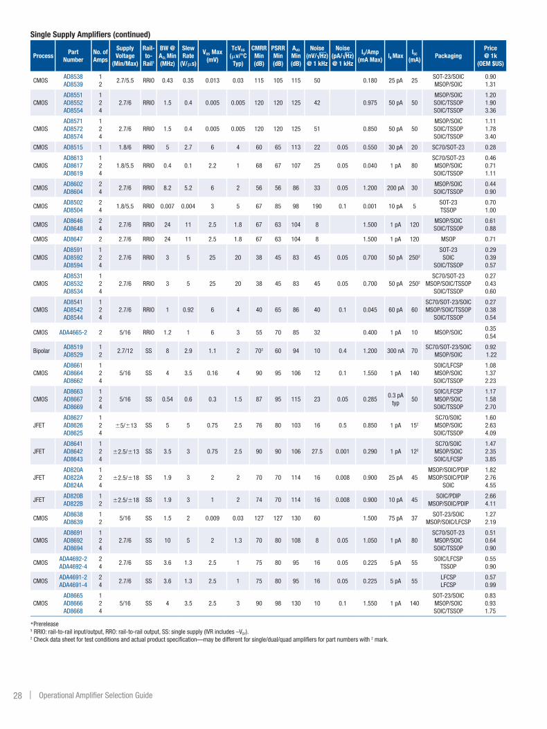
Single Supply Amplifiers (continued)
ProcessPart
NumberNo. of Amps
Supply Voltage
(Min/Max)
Rail-to-
Rail1
BW @ ACL Min
(MHz)
Slew Rate
(V/ms)
VOS Max
(mV)
TcVOS (mv/°C
Typ)
CMRR Min (dB)
PSRR Min (dB)
AVO Min (dB)
Noise (nV/√Hz) @ 1 kHz
Noise (pA/√Hz) @ 1 kHz
IS/Amp
(mA Max)IB Max
ISC
(mA)Packaging
Price @ 1k
(OEM $US)
CMOSAD8538 AD8539
1 2
2.7/5.5 RRIO 0.43 0.35 0.013 0.03 115 105 115 50 0.180 25 pA 25SOT-23/SOIC MSOP/SOIC
0.90 1.31
CMOSAD8551 AD8552 AD8554
1 2 4
2.7/6 RRIO 1.5 0.4 0.005 0.005 120 120 125 42 0.975 50 pA 50MSOP/SOIC SOIC/TSSOP SOIC/TSSOP
1.20 1.90 3.36
CMOSAD8571 AD8572 AD8574
1 2 4
2.7/6 RRIO 1.5 0.4 0.005 0.005 120 120 125 51 0.850 50 pA 50MSOP/SOIC SOIC/TSSOP SOIC/TSSOP
1.11 1.78 3.40
CMOS AD8515 1 1.8/6 RRIO 5 2.7 6 4 60 65 113 22 0.05 0.550 30 pA 20 SC70/SOT-23 0.28
CMOSAD8613 AD8617 AD8619
1 2 4
1.8/5.5 RRIO 0.4 0.1 2.2 1 68 67 107 25 0.05 0.040 1 pA 80SC70/SOT-23 MSOP/SOIC SOIC/TSSOP
0.46 0.71 1.11
CMOSAD8602 AD8604
2 4
2.7/6 RRIO 8.2 5.2 6 2 56 56 86 33 0.05 1.200 200 pA 30MSOP/SOIC SOIC/TSSOP
0.44 0.90
CMOSAD8502 AD8504
2 4
1.8/5.5 RRIO 0.007 0.004 3 5 67 85 98 190 0.1 0.001 10 pA 5SOT-23 TSSOP
0.70 1.00
CMOSAD8646 AD8648
2 4
2.7/6 RRIO 24 11 2.5 1.8 67 63 104 8 1.500 1 pA 120MSOP/SOIC SOIC/TSSOP
0.61 0.88
CMOS AD8647 2 2.7/6 RRIO 24 11 2.5 1.8 67 63 104 8 1.500 1 pA 120 MSOP 0.71
CMOSAD8591 AD8592 AD8594
1 2 4
2.7/6 RRIO 3 5 25 20 38 45 83 45 0.05 0.700 50 pA 2502
SOT-23 SOIC
SOIC/TSSOP
0.29 0.39 0.57
CMOSAD8531 AD8532 AD8534
1 2 4
2.7/6 RRIO 3 5 25 20 38 45 83 45 0.05 0.700 50 pA 2502
SC70/SOT-23 MSOP/SOIC/TSSOP
SOIC/TSSOP
0.27 0.43 0.60
CMOSAD8541 AD8542 AD8544
1 2 4
2.7/6 RRIO 1 0.92 6 4 40 65 86 40 0.1 0.045 60 pA 60SC70/SOT-23/SOIC MSOP/SOIC/TSSOP
SOIC/TSSOP
0.27 0.38 0.54
CMOS ADA4665-2 2 5/16 RRIO 1.2 1 6 3 55 70 85 32 0.400 1 pA 10 MSOP/SOIC0.35 0.54
BipolarAD8519 AD8529
1 2
2.7/12 SS 8 2.9 1.1 2 702 60 94 10 0.4 1.200 300 nA 70SC70/SOT-23/SOIC
MSOP/SOIC0.92 1.22
CMOSAD8661 AD8664 AD8662
1 2 4
5/16 SS 4 3.5 0.16 4 90 95 106 12 0.1 1.550 1 pA 140SOIC/LFCSP MSOP/SOIC SOIC/TSSOP
1.08 1.37 2.23
CMOSAD8663 AD8667 AD8669
1 2 4
5/16 SS 0.54 0.6 0.3 1.5 87 95 115 23 0.05 0.2850.3 pA
typ50
SOIC/LFCSP MSOP/SOIC SOIC/TSSOP
1.17 1.58 2.70
JFETAD8627 AD8626 AD8625
1 2 4
65/613 SS 5 5 0.75 2.5 76 80 103 16 0.5 0.850 1 pA 152
SC70/SOIC MSOP/SOIC SOIC/TSSOP
1.60 2.63 4.09
JFETAD8641 AD8642 AD8643
1 2 4
62.5/613 SS 3.5 3 0.75 2.5 90 90 106 27.5 0.001 0.290 1 pA 122
SC70/SOIC MSOP/SOIC SOIC/LFCSP
1.47 2.35 3.85
JFETAD820A AD822A AD824A
1 2 4
62.5/618 SS 1.9 3 2 2 70 70 114 16 0.008 0.900 25 pA 45MSOP/SOIC/PDIP MSOP/SOIC/PDIP
SOIC
1.82 2.76 4.55
JFETAD820B AD822B
1 2 62.5/618 SS 1.9 3 1 2 74 70 114 16 0.008 0.900 10 pA 45
SOIC/PDIP MSOP/SOIC/PDIP
2.66 4.11
CMOSAD8638 AD8639
1 2
5/16 SS 1.5 2 0.009 0.03 127 127 130 60 1.500 75 pA 37SOT-23/SOIC
MSOP/SOIC/LFCSP1.27 2.19
CMOSAD8691 AD8692 AD8694
1 2 4
2.7/6 SS 10 5 2 1.3 70 80 108 8 0.05 1.050 1 pA 80SC70/SOT-23 MSOP/SOIC SOIC/TSSOP
0.51 0.64 0.90
CMOSADA4692-2 ADA4692-4
2 4
2.7/6 SS 3.6 1.3 2.5 1 75 80 95 16 0.05 0.225 5 pA 55SOIC/LFCSP
TSSOP0.55 0.90
CMOSADA4691-2 ADA4691-4
2 4
2.7/6 SS 3.6 1.3 2.5 1 75 80 95 16 0.05 0.225 5 pA 55LFCSP LFCSP
0.57 0.99
CMOSAD8665 AD8666 AD8668
1 2 4
5/16 SS 4 3.5 2.5 3 90 98 130 10 0.1 1.550 1 pA 140SOT-23/SOIC MSOP/SOIC SOIC/TSSOP
0.83 0.93 1.75
*Prerelease 1 RRIO: rail-to-rail input/output, RRO: rail-to-rail output, SS: single supply (IVR includes –VSY).2 Check data sheet for test conditions and actual product specification—may be different for single/dual/quad amplifiers for part numbers with 2 mark.

| 29www.analog.com/opamps
Precision Amplifiers (VOS < 1 mV, Bandwidth < 50 MHz)
Rail-to-Rail Output Amplifiers AD8641: Low Power, Rail-to-Rail Output Precision JFET Amplifier
The AD8641/AD8642/AD8643 are low power, precision JFET input amplifiers featuring extremely low input bias current and rail-to-rail output. The ability to swing nearly rail-to-rail at the input and rail-to-rail at the output enables designers to buffer CMOS DACs, ASICs, and other wide output swing devices in single-supply systems. The outputs remain stable with capacitive loads of more than 500 pF.
Features
•Low supply current: 250 mA max
•Very low input bias current: 1 pA max
•Low offset voltage: 750 mV max
•Single-supply operation: 5 V to 26 V
•Dual-supply operation: 62.5 V to 613 V
•Rail-to-rail output
•Unity-gain stable
Applications
•Line-/battery-powered instruments
•Precision current sensing
•Medical instrumentation
• Industrial controls
•Precision filters
•Portable audio
•ATEOutput saturation voltage vs. load current.
ADA4691-2 Dual, Low Power, Wideband, Low Noise, Rail-to-Rail Output Amplifier
The ADA4691-2 is a dual, rail-to-rail output, single-supply amplifier featuring low power, wide bandwidth, and low noise. The ADA4691-2 has two independent shutdown pins, allowing further reduction in supply current. These amplifiers are ideal for a wide variety of applications. Audio preamps, filters, IR/photodiode amplifiers, charge amps, and high impedance sensors all benefit from this combination of performance features.
Features
•Low power: 180 µA typical
•Low distortion: 0.003% THD + N
•Low noise: 16 nV/√Hz typical
•3.6 MHz bandwidth
•Offset voltage: 500 µV typical
Applications
•Portable audio
•Portable instrumentation and medical devices
•Photodiode amplifiers
•Sensor amplifiers
•Low-side current sense
•ADC drivers
•Active filters
•Sample-and-hold
•Automotive sensorsNoise vs. frequency.
SA
TU
RA
TIO
N V
OLT
AG
E (m
V)
1
10
100
1000
10000
0.001 0.01 0.1 1 10 100
LOAD CURRENT (mA)
–VSY – VOL
VSY – VOH
VSY = ±13V
1
0.1
0.01
0.00110 100 1k 10k 20k
TH
D +
N (%
)
FREQUENCY (Hz)
ADA4692-2VSY = ±2.5VAV = –1TA = 25°C
RL = 600
RL = 2k

30 | Operational Amplifier Selection Guide
Rail-to-Rail Output Amplifiers
ProcessPart
NumberNo. of Amps
Supply Voltage
(Min/Max)
Rail-to-
Rail1
BW @ ACL Min
(MHz)
Slew Rate
(V/ms)
VOS Max
(mV)
TcVOS (mv/°C
Typ)
CMRR Min (dB)
PSRR Min (dB)
AVO Min (dB)
Noise (nV/√Hz) @ 1 kHz
Noise (pA/√Hz) @ 1 kHz
IS/Amp
(mA Max)IB Max Packaging
Price @ 1k
(OEM $US)
Bipolar AD8675 1 ±5/±18 RRO 10 2.5 0.075 0.2 114 120 123 2.8 0.32 2.900 2 nA MSOP/SOIC 1.18
Bipolar AD8676A 2 ±5/±18 RRO 10 2.5 0.1 0.2 111 106 123 2.8 0.32 3.400 2 nA MSOP/SOIC 1.66
Bipolar AD8676B 2 ±5/±18 RRO 10 2.5 0.05 0.2 111 106 123 2.8 0.32 3.400 2 nA MSOP/SOIC 2.14
CMOSAD8605 AD8606 AD8608
1 2 4
2.7/6 RRIO 10 5 0.3 1 85 80 109 8 0.01 1.200 1 pAWLCSP/SOT-23
WLCSP/MSOP/SOIC SOIC/TSSOP
0.68 1.19 1.58
CMOSAD8691 AD8692 AD8694
1 2 4
2.7/6 SS 10 5 2 1.3 70 80 108 8 0.05 1.050 1 pASC70/SOT-23 MSOP/SOIC SOIC/TSSOP
0.51 0.64 0.90
CMOSAD8646 AD8648
2 4
2.7/6 RRIO 24 11 2.5 1.8 67 63 104 8 1.500 1 pAMSOP/SOIC SOIC/TSSOP
0.61 0.88
CMOS AD8647 2 2.7/6 RRIO 24 11 2.5 1.8 67 63 104 8 1.500 1 pA MSOP 0.71
BipolarOP162 OP262 OP462
1 2 4
2.7/12 SS 15 13 0.325 1 70 60 97 9.5 0.4 0.800 500 nAMSOP/SOIC/TSSOP
SOIC/TSSOP SOIC/TSSOP
1.69 2.23 4.03
BipolarAD8519 AD8529
1 2
2.7/12 SS 8 2.9 1.1 2 702 60 94 10 0.4 1.200 300 nASC70/SOT-23/SOIC
MSOP/SOIC0.92 1.22
CMOSAD8615 AD8616 AD8618
1 2 4
2.7/6 RRIO 24 12 0.5 1.5 80 70 105 10 0.05 1.300 1 pASOT-23
MSOP/SOIC SOIC/TSSOP
0.76 1.29 2.29
CMOSAD8665 AD8666 AD8668
1 2 4
5/16 SS 4 3.5 2.5 3 90 98 130 10 0.1 1.550 1 pASOT-23/SOIC MSOP/SOIC SOIC/TSSOP
0.83 0.93 1.75
BipolarAD8622 AD8624
2 4 62.5/618 RRO 0.56 0.48 0.125 0.5 125 125 125 11 0.15 0.250 200 pA
MSOP/SOIC LFCSP/TSSOP
2.30 3.75
CMOSAD8661 AD8662 AD8664
1 2 4
5/16 SS 4 3.5 0.16 4 90 95 106 12 0.1 1.550 1 pASOIC/LFCSP MSOP/SOIC SOIC/TSSOP
1.08 1.37 2.23
JFETAD8627 AD8626 AD8625
1 2 4
65/613 SS 5 5 0.75 2.5 76 80 103 16 0.5 0.850 1 pAWLCSP/SOIC MSOP/SOIC SOIC/TSSOP
1.60 2.63 4.09
JFETAD820A AD822A AD824A
1 2 4
62.5/618 SS 1.9 3 2 2 70 70 114 16 0.008 0.900 25 pAMSOP/SOIC
MSOP/SOIC/PDIP SOIC
1.82 2.76 4.55
JFETAD820B AD822B
1 2 62.5/618 SS 1.9 3 1 2 74 70 114 16 0.008 0.900 10 pA
SOIC/PDIP MSOP/SOIC/PDIP
2.66 4.11
CMOSADA4692-2 ADA4692-4
2 4
2.7/6 SS 3.6 1.3 2.5 1 75 80 95 16 0.05 0.225 5 pASOIC/LFCSP
TSSOP0.55 0.90
CMOSADA4691-2 ADA4691-4
2 4
2.7/6 SS 3.6 1.3 2.5 1 75 80 95 16 0.05 0.225 5 pAWLCSP/LFCSP
LFCSP0.57 0.99
CMOSAD8628 AD8629 AD8630
1 2 4
2.7/6 RRIO 2.5 1 0.005 0.002 120 115 125 22 0.850 100 pASOT-23/SOIC MSOP/SOIC SOIC/TSSOP
0.96 1.47 2.73
CMOS AD8515 1 1.8/6 RRIO 5 2.7 6 4 60 65 113 22 0.05 0.550 30 pA SC70/SOT-23 0.28
CMOSAD8663 AD8667 AD8669
1 2 4
5/16 SS 0.54 0.6 0.3 1.5 87 95 115 23 0.05 0.2850.3 pA
typ
SOIC/LFCSP MSOP/SOIC SOIC/TSSOP
1.17 1.58 2.70
CMOSAD8603 AD8607 AD8609
1 2 4
1.8/6 RRIO 0.4 0.1 0.3 1 85 80 112 25 0.05 0.040 1 pASOT-23
MSOP/SOIC SOIC/TSSOP
0.68 1.02 1.85
BipolarADA4091-2 ADA4091-4
2 4 61.35/618 RRIO 1.27 0.46 0.25 2.5 104 108 116 25 0.250 55 nA
SOIC/LFCSP LFCSP/TSSOP
2.22 3.50
CMOSAD8613 AD8617 AD8619
1 2 4
1.8/5.5 RRIO 0.4 0.1 2.2 1 68 67 107 25 0.05 0.040 1 pASC70/SOT-23 MSOP/SOIC SOIC/TSSOP
0.46 0.71 1.11
BipolarAD8565 AD8566 AD8567
1 2 4
4.5/16 RRIO 5 6 10 5 54 70 69 26 0.82 0.850 600 nASC70 MSOP
LFCSP/TSSOP
0.56 0.71 0.93
BipolarOP196 OP296 OP496
1 2 4
3/15 RRIO 0.45 0.3 0.3 1.5 652 110 109 26 0.19 0.060 50 nASOIC
SOIC/TSSOP/PDIP SOIC/TSSOP/PDIP
1.56 1.85 2.66

| 31www.analog.com/opamps
Rail-to-Rail Output Amplifiers (continued)
ProcessPart
NumberNo. of Amps
Supply Voltage
(Min/Max)
Rail-to-
Rail1
BW @ ACL Min
(MHz)
Slew Rate
(V/ms)
VOS Max
(mV)
TcVOS (mv/°C
Typ)
CMRR Min (dB)
PSRR Min (dB)
AVO Min (dB)
Noise (nV/√Hz) @ 1 kHz
Noise (pA/√Hz) @ 1 kHz
IS/Amp
(mA Max)IB Max Packaging
Price @ 1k
(OEM $US)
JFETAD8641 AD8642 AD8643
1 2 4
62.5/613 SS 3.5 3 0.75 2.5 90 90 106 27.5 0.0005 0.290 1 pASC70/SOIC MSOP/SOIC SOIC/LFCSP
1.47 2.35 3.85
CMOS ADA4665-2 2 5/16 RRIO 1.2 1 6 3 55 70 85 32 0.400 1 pA MSOP/SOIC 0.70
CMOSAD8601A AD8602A AD8604A
1 2 4
2.7/6 RRIO 8.2 5.2 0.5 2 74 67 89 33 0.05 1.200 60 pASOT-23
MSOP/SOIC SOIC/TSSOP
0.62 0.83 1.13
CMOSAD8602 AD8604
2 4
2.7/6 RRIO 8.2 5.2 6 2 56 56 86 33 0.05 1.200 200 pAMSOP/SOIC SOIC/TSSOP
0.44 0.90
CMOSAD8541 AD8542 AD8544
1 2 4
2.7/6 RRIO 1 0.92 6 4 40 65 86 40 0.1 0.045 60 pASC70/SOT-23/SOIC MSOP/SOIC/TSSOP
SOIC/TSSOP
0.27 0.38 0.54
BipolarOP191 OP291 OP491
1 2 4
2.7/12 RRIO 1.5 0.5 0.5 1.1 75 80 88 42 0.8 0.420 65 nASOIC SOIC
SOIC/TSSOP/PDIP
1.69 2.22 3.60
CMOSAD8551 AD8552 AD8554
1 2 4
2.7/6 RRIO 1.5 0.4 0.005 0.005 120 120 125 42 0.975 50 pAMSOP/SOIC SOIC/TSSOP SOIC/TSSOP
1.20 1.90 3.36
CMOSAD8657 AD8659*
2 4
2.7/18 RRIO 0.175 0.3 0.3 4 95 105 110 50 0.022 5 pAMSOP/SOIC SOIC/LFCSP
0.951.35
CMOSAD85052 AD8506 AD8508
1 2 4
1.8/5.5 RRIO 0.095 0.013 2.5 2 90 100 105 45 0.015 0.020 10 pASOT-23 MSOP TSSOP
0.59 0.71 1.20
CMOSAD8591 AD8592 AD8594
1 2 4
2.7/6 RRIO 3 5 25 20 38 45 83 45 0.05 0.700 50 pASOT-23
SOIC SOIC/TSSOP
0.29 0.39 0.57
CMOSAD8531 AD8532 AD8534
1 2 4
2.7/6 RRIO 3 5 25 20 38 45 83 45 0.05 0.700 50 pASC70/SOT-23
MSOP/SOIC/TSSOP SOIC/TSSOP
0.27 0.43 0.60
CMOSAD8538 AD8539
1 2
2.7/5.5 RRIO 0.43 0.35 0.013 0.03 115 105 115 50 0.180 25 pASOT-23/SOIC MSOOP/SOIC
0.90 1.31
CMOSAD8571 AD8572 AD8574
1 2 4
2.7/6 RRIO 1.5 0.4 0.005 0.005 120 120 125 51 0.850 50 pAMSOP/SOIC SOIC/TSSOP SOIC/TSSOP
1.11 1.78 3.40
CMOSAD8638 AD8639
1 2
5/16 SS 1.5 2 0.009 0.03 127 127 130 60 1.500 75 pASOT-23/SOIC
MSOP/SOIC/LFCSP1.27 2.19
CMOSADA4505-12 ADA4505-2 ADA4505-4
1 2 4
1.8/5.5 RRIO 0.050 0.006 3 2 90 100 105 65 0.02 0.010 2 pAWLCSP/SOT-23 WLCSP/MSOP WLCSP/TSSOP
0.55 0.67 1.15
BipolarOP281 OP481
2 4
2.7/12 SS 0.105 0.028 1.5 10 65 76 74 85 1 0.005 10 nASOIC/TSSOP SOIC/TSSOP
2.74 3.58
CMOSADA4051-1 ADA4051-2
1 2
1.8/5.5 RRIO 0.125 0.06 0.015 0.02 110 110 115 95 0.1 0.017 70 pASC70/SOT-23 MSOP/LFCSP
0.93 1.47
CMOS AD8500 1 1.8/5.5 RRIO 0.007 0.004 1 3 75 90 98 190 0.1 0.001 10 pA SC70 0.71
CMOSAD8502 AD8504
2 4
1.8/5.5 RRIO 0.007 0.004 3 5 67 85 98 190 0.1 0.001 10 pASOT-23 TSSOP
0.70 1.00
CMOSAD8655 AD8656
1 2
2.7/5.5 RRIO 28 11 0.25 0.4 85 88 100 2.72 4.500 10 pAMSOP/SOIC MSOP/SOIC
0.71 1.11
CMOSAD8651 AD8652
1 2
2.7/5.5 RRIO 50 41 0.35 4 80 76 100 4.52 0.025 14.000 10 pAMSOP/SOIC MSOP/SOIC
1.13 1.99
*Prerelease 1 RRIO: rail-to-rail input/output, RRO: rail-to-rail output, SS: single supply (IVR includes –VSY).2 Check data sheet for test conditions and actual product specification—may be different for single/dual/quad amplifiers for part numbers with 2 mark.

32 | Operational Amplifier Selection Guide
Rail-to-Rail Input/Output Amplifiers
ProcessPart
NumberNo. of Amps
Supply Voltage
(Min/Max)Rail-to-Rail1
BW @ ACL Min
(MHz)
Slew Rate
(V/ms)
VOS
(mV Max)
TcVOS (mv/°C
Typ)
BW @ ACL Min
(MHz)
Slew Rate
(V/ms)
( )
TcVOS (mv/°C
Typ)
IS/Amp
(mA Max)IB Max Packaging
Price @ 1k
(OEM $US)
CMOSADA4528-1 ADA4528-2*
12
2.2/5.5 RRIO 4 0.4 0.0025 0.015 115 120 130 5.3 1.500 100 pA MSOP/LFCSP1.15 1.90
CMOSAD8605 AD8606 AD8608
1 2 4
2.7/6 RRIO 10 5 0.3 1 85 80 109 8 1.200 1 pAWLCSP/SOT-23
WLCSP/MSOP/SOIC SOIC/TSSOP
0.68 1.19 1.58
CMOSAD8646 AD8648
2 4
2.7/6 RRIO 24 11 2.5 1.8 67 63 104 8 1.500 1 pAMSOP/SOIC SOIC/TSSOP
0.61 0.88
CMOS AD8647 SD 2 2.7/6 RRIO 24 11 2.5 1.8 67 63 104 8 1.500 1 pA MSOP 0.71
CMOSAD8615 AD8616 AD8618
1 2 4
2.7/6 RRIO 24 12 0.5 1.5 80 70 105 10 1.300 1 pASOT-23
MSOP/SOIC SOIC/MSSOP
0.76 1.29 2.29
CMOSAD8628 AD8629 AD8630
1 2 4
2.7/6 RRIO 2.5 1 0.005 0.002 120 115 125 22 0.850 100 pASOT-23/SOIC MSOP/SOIC SOIC/TSSOP
0.96 1.47 2.73
CMOS AD8515 1 1.8/6 RRIO 5 2.7 6 4 60 65 113 22 0.550 30 pA SC70/SOT-23 0.28
CMOSAD8603 AD8607 AD8609
1 2 4
1.8/6 RRIO 0.4 0.1 0.3 1 85 80 112 25 0.040 1 pASOT-23
MSOP/SOIC SOIC/MSSOP
0.68 1.02 1.85
BipolarADA4091-2 ADA4091-4
2 4 61.35/618 RRIO 1.27 0.46 0.25 2.5 104 108 116 25 0.250 55 nA
SOIC/LFCSP LFCSP/TSSOP
2.22 3.50
CMOSAD8613 AD8617 AD8619
1 2 4
1.8/5.5 RRIO 0.4 0.1 2.2 1 68 67 107 25 0.040 1 pASC70/SOT-23 MSOP/SOIC SOIC/TSSOP
0.46 0.71 1.11
*Prerelease
Precision Amplifiers (VOS < 1 mV, Bandwidth < 50 MHz)
Rail-to-Rail Input/Output Amplifiers AD8656: Low power, Precision RRIO CMOS Amplifier
The AD8656 provides low noise (2.7 nV/√Hz @ 10 kHz), low THD + N (0.0007%), and high precision performance (250 µV max over VCM) to low voltage applications. The ability to swing rail-to-rail at the input and output enables designers to buffer analog-to-digital converters (ADCs) and other wide dynamic range devices in single-supply systems.
Features
•Low noise: 2.7 nV/√Hz @ f = 10 kHz
•Low offset voltage: 250 mV max over VCM (common-mode voltage)
•Offset voltage drift:; 0.4 mV/°C typ and 2.3 µV/°C max
•Bandwidth: 28 MHz
•Rail-to-rail input/output
•Unity-gain stable
Applications
•ADC and DAC buffers
•Audio
• Industrial controls
•Precision filters
•Digital scales
•Strain gages
•PLL filters No phase reversal.
T
2
VS = ±2.5VCL = 50pFGAIN = +1
1V/D
IV
20s/DIV
VIN
VOUT
AVo Min

| 33www.analog.com/opamps
Rail-to-Rail Input/Output Amplifiers (continued)
ProcessPart
NumberNo. of Amps
Supply Voltage
(Min/Max)Rail-to-Rail1
BW @ ACL Min
(MHz)
Slew Rate
(V/ms)
VOS
(mV Max)
TcVOS (mv/°C
Typ)
BW @ ACL Min
(MHz)
Slew Rate
(V/ms)
TcVOS (mv/°C
Typ)
IS/Amp
(mA Max)IB Max Packaging
Price @ 1k
(OEM $US)
BipolarAD8565 AD8566 AD8567
1 2 4
4.5/16 RRIO 5 6 10 5 54 70 69 26 0.850 600 nASC70 MSOP
LFCSP/TSSOP
0.56 0.71 0.93
CBCMOSOP196 OP296 OP496
1 2 4
3/15 RRIO 0.45 0.3 0.3 1.5 652 110 109 26 0.060 50 nASOIC
SOIC/TSSOP/PDIP SOIC/TSSOP/PDIP
1.56 1.85 2.66
BiPolarADA4092-2* ADA4092-4
2 4 61.35/618 RRIO 1.4 0.4 1.5 2.5 90 98 116 30 0.250 60 nA
SOIC/LFCSP TSSOP
1.35 2.50
CMOS ADA4665-2 2 5/16 RRIO 1.2 1 6 3 55 70 85 32 0.400 1 pA MSOP/SOIC 0.70
CMOSAD8601A AD8602A AD8604A
1 2 4
2.7/6 RRIO 8.2 5.2 0.5 2 74 67 89 33 1.200 60 pASOT-23
MSOP/SOIC SOIC/TSSOP
0.62 0.83 1.13
CMOSAD8602 AD8604
2 4
2.7/6 RRIO 8.2 5.2 6 2 56 56 86 33 1.200 200 pAMSOP/SOIC SOIC/TSSOP
0.44 0.90
CMOSAD8541 AD8542 AD8544
1 2 4
2.7/6 RRIO 1 0.92 6 4 40 65 86 40 0.045 60 pASC70/SOT-23/SOIC MSOP/SOIC/TSSOP
SOIC/TSSOP
0.27 0.38 0.54
CMOSOP191 OP291 OP491
1 2 4
2.7/12 RRIO 1.5 0.5 0.5 1.1 75 80 88 42 0.420 65 nASOIC SOIC
SOIC/TSSOP/PDIP
1.69 2.22 3.60
CMOSAD8551 AD8552 AD8554
1 2 4
2.7/6 RRIO 1.5 0.4 0.005 0.005 120 120 125 42 0.975 50 pAMSOP/SOIC SOIC/TSSOP SOIC/TSSOP
1.20 1.90 3.36
CMOSAD8657 AD8659*
2 4
2.7/18 RRIO 0.175 0.3 0.3 4 95 105 110 50 0.022 5 pAMSOP/SOIC SOIC/LFCSP
0.95 1.35
CMOSAD85052 AD8506 AD8508
1 2 4
1.8/5.5 RRIO 0.095 0.013 2.5 2 90 100 105 45 0.020 10 pAWLCSP/SOT-23 WLCSP/MSOP WLCSP/TSSOP
0.59 0.71 1.20
CMOSAD8591 AD8592 AD8594
1 2 4
2.7/6 RRIO 3 5 25 20 38 45 83 45 0.700 50 pASOT-23
SOIC SOIC/TSSOP
0.29 0.39 0.57
CMOSAD8531 AD8532 AD8534
1 2 4
2.7/6 RRIO 3 5 25 20 38 45 83 45 0.700 50 pASC70/SOT-23 MSOP/SOIC SOIC/TSSOP
0.27 0.43 0.60
CMOSAD8538 AD8539
1 2
2.7/5.5 RRIO 0.43 0.35 0.013 0.03 115 105 115 50 0.180 25 pASOT-23/SOIC MSOP/SOIC
0.90 1.31
CMOSAD8571 AD8672 AD8574
1 2 4
2.7/6 RRIO 1.5 0.4 0.005 0.005 120 120 125 51 0.850 50 pAMSOP/SOIC SOIC/TSSOP SOIC/TSSOP
1.11 1.78 3.40
CMOSADA4505-12 ADA4505-2 ADA4505-4
1 2 4
1.8/5.5 RRIO 0.050 0.006 3 2 90 100 105 65 0.010 2 pAWLCSP/SOT-23 WLCSP/MSOP WLCSP/TSSOP
0.55 0.67 1.15
CMOSADA4051-1 ADA4051-2
1 2
1.8/5.5 RRIO 0.125 0.06 0.015 0.02 110 110 115 95 0.017 70 pASC70/SOT-23 MSOP/LFCSP
0.93 1.47
CMOS AD8500 1 1.8/5.5 RRIO 0.007 0.004 1 3 75 90 98 190 0.001 10 pA SC70 0.71
CMOSAD8502 AD8504
2 4
1.8/5.5 RRIO 0.007 0.004 3 5 67 85 98 190 0.001 10 pASOT-23 TSSOP
0.70 1.00
CMOSAD8655 AD8656
1 2
2.7/5.5 RRIO 28 11 0.25 0.4 85 88 100 2.72 4.500 10 pAMSOP/SOIC MSOP/SOIC
0.71 1.11
CMOSAD8651 AD8652
1 2
2.7/5.5 RRIO 50 41 0.35 4 80 76 100 4.52 14.000 10 pAMSOP/SOIC MSOP/SOIC
1.13 1.99
*Prerelease 1 RRIO: rail-to-rail input/output, RRO: rail-to-rail output, SS: single supply (IVR includes –VSY).2 Check data sheet for test conditions and actual product specification—may be different for single/dual/quad amplifiers for part numbers with 2 mark.
AVo Min
(dB)

34 | Operational Amplifier Selection Guide
Amplifiers (Bandwidth < 50 MHz)
Low Cost Amplifiers AD8541: General-Purpose CMOS Rail-to-Rail Amplifier
The AD8541/AD8542/AD8544 are single, dual, and quad rail-to-rail input and output single-supply amplifiers featuring very low supply current and 1 MHz bandwidth. All are guaranteed to operate from a 2.7 V single supply, as well as a 5 V supply. These parts provide 1 MHz bandwidth at a low current consumption of 45 mA per amplifier.
Features
•Single-supply operation: 2.7 V to 5.5 V
•Low supply current: 45 mA/amplifier
•Wide bandwidth: 1 MHz
•No phase reversal
•Low input currents: 4 pA
•Unity-gain stable
•Rail-to-rail Input/Output
Applications
•Sensor interfaces
•Piezoelectric transducer amplifiers
•Medical instrumentation
•Mobile communications
•Audio outputs
•Portable systems
ADA4692-2: Dual, Low Power, Wideband, Low Noise, Rail-to-Rail Output Amplifier
The ADA4692-2 is a dual, rail-to-rail output, single-supply amplifier featuring low power, wide bandwidth, and low noise. The ADA4691-2 has two independent shutdown pins, allowing further reduction in supply current. These amplifiers are ideal for a wide variety of applications. Audio preamps, filters, IR/photodiode amplifiers, charge amps, and high impedance sensors all benefit from this combination of performance features.
Features
•Low power: 180 µA typical
•Low distortion: 0.003% THD + N
•Low noise: 16 nV/√Hz typical
•3.6 MHz bandwidth
•Offset voltage: 500 µV typical
Applications
•Portable audio
•Portable instrumentation and medical devices
•Photodiode amplifiers
•Sensor amplifiers
•Low-side current sense
•ADC drivers
•Active filters
•Sample-and-hold
•Automotive sensors
High input impedance application—photodiode amplifier.
Channel separation vs. frequency.
AD85414
6
7
3
2
D
ORV+
2.5VREF
C100pF
R10M
2.5VREF
VOUT
–80
–90
–100
–110
–120
–130
–140100 1k 10k 100k
CH
AN
NE
L S
EPA
RA
TIO
N (d
B)
FREQUENCY (Hz)
ADA4692-2VSY = ±2.5VVIN = 2.8V p-pAV = +1TA = 25°C

| 35www.analog.com/opamps
Low Cost Amplifiers
ProcessPart
NumberNo. of Amps
Supply Voltage
(Min/Max)Rail-to-Rail1
BW @ ACL Min
(MHz)
Slew Rate
(V/ms)
VOS Max
(mV)
TcVOS (mv/°C
Typ)
CMRRMin(dB)
PSRRMin(dB)
AVO Min (dB)
Noise (nV/√Hz)@ 1kHz
IS/Amp
(mA Max)IB Max Packaging
Price @ 1k
(OEM $US)
CMOS AD8515 1 1.8/6 RRIO 5 2.7 6 4 60 65 113 22 0.550 30 pA SC70/SOT-23 0.28
CMOS ADA4665-2 2 5/16 RRIO 1.2 1 6 3 55 70 85 32 0.400 1 pA MSOP/SOIC 0.70
CMOSAD8541 AD8542 AD8544
1 2 4
2.7/6 RRIO 1 0.92 6 4 40 65 86 40 0.045 60 pASC70/SOT-23 MSOP/SOIC SOIC/TSSOP
0.27 0.38 0.54
CMOSAD8546 AD8548
24
2.7/18 RRIO 0.2 0.07 3 0.025 80 90 88 50 0.022 100 pA MSOP/SOIC/LFCSP0.781.05
CMOSAD8531 AD8532 AD8534
1 2 4
2.7/6 RRIO 3 5 25 20 38 45 83 45 0.700 50 pASC70/SOT-23 MSOP/SOIC SOIC/TSSOP
0.27 0.43 0.60
CMOSAD8591 AD8592 AD8594
1 2 4
2.7/6 RRIO 3 5 25 20 38 45 83 45 0.700 50 pASOT-23
SOIC SOIC/TSSOP
0.29 0.39 0.57
JFETADTL082A ADTL084A
2 4
64/618 5 20 5.5 10 80 80 100 16 1.800 100 pAMSOP/SOIC SOIC/TSSOP
0.42 0.90
CMOSAD8602 AD8604
2 4
2.7/6 RRIO 8.2 5.2 6 2 56 56 86 33 1.200 200 pAMSOP/SOIC SOIC/TSSOP
0.44 0.90
CMOSAD8613 AD8617 AD8619
1 2 4
1.8/5.5 RRIO 0.4 0.1 2.2 1 68 67 107 25 0.040 1 pASC70/SOT-23 MSOP/SOIC SOIC/TSSOP
0.46 0.71 1.11
CMOSAD8691 AD8692 AD8694
1 2 4
2.7/6 SS 10 5 2 1.3 70 80 108 8 1.050 1 pASC70/SOT-23 MSOP/SOIC SOIC/TSSOP
0.51 0.64 0.90
CMOSADA4505-12 ADA4505-2 ADA4505-4
1 2 4
1.8/5.5 RRIO 0.050 0.006 3 2 90 100 105 65 0.010 2 pAWLCSP/SOT-23 WLCSP/MSOP WLCSP/TSSOP
0.55 0.67 1.15
CMOSADA4692-2 ADA4692-4
2 4 2.7/6 SS 3.6 1.3 2.5 1 75 80 95 16 0.225 5 pA
SOIC/LFCSP TSSOP
0.55 0.90
BipolarAD8565 AD8566 AD8567
1 2 4
4.5/16 RRIO 5 6 10 5 54 70 69 26 0.850 600 nASC70 MSOP
LFCSP/TSSOP
0.56 0.71 0.93
CMOSADA4691-2 ADA4691-4
2 4
2.7/6 SS 3.6 1.3 2.5 1 75 80 95 16 0.225 5 pAWLCSP/LFCSP
LFCSP0.57 0.99
CMOSAD85052 AD8506 AD8508
1 2 4
1.8/5.5 RRIO 0.095 0.013 2.5 2 90 100 105 45 0.020 10 pAWLCSP/SOT-23 WLCSP/MSOP WLCSP/TSSOP
0.59 0.71 1.20
CMOSAD8646 AD8648
2 4
2.7/6 RRIO 24 11 2.5 1.8 67 63 104 8 1.500 1 pAMSOP/SOIC SOIC/TSSOP
0.61 0.88
CMOSAD8601A AD8602A AD8604A
1 2 4
2.7/6 RRIO 8.2 5.2 0.5 2 74 67 89 33 1.200 60 pASOT-23
MSOP/SOIC SOIC/TSSOP
0.62 0.83 1.13
CMOSAD8603 AD8607 AD8609
1 2 4
1.8/6 RRIO 0.4 0.1 0.3 1 85 80 112 25 0.040 1 pASOT-23
MSOP/SOIC SOIC/TSSOP
0.68 1.02 1.85
CMOSAD8605 AD8606 AD8608
1 2 4
2.7/6 RRIO 10 5 0.3 1 85 80 109 8 1.200 1 pAWLCSP/SOT-23
WLCSP/MSOP/SOIC SOIC/TSSOP
0.68 1.19 1.58
CMOSAD8502 AD8504
2 4
1.8/5.5 RRIO 0.007 0.004 3 5 67 85 98 190 0.001 10 pASOT-23 TSSOP
0.70 1.00
1 RRIO: rail-to-rail input/output, RRO: rail-to-rail output, SS: single supply (IVR includes –VSY).2 Check data sheet for test conditions and actual product specification—may be different for single/dual/quad amplifiers for part numbers with 2 mark.
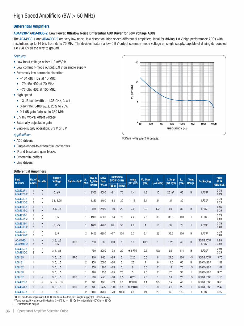
36 | Operational Amplifier Selection Guide
Differential Amplifiers
Part Number
No. of Amps
DisableSupply Voltage
(V)Rail-to-Rail1 ACL
Min
BW @ ACL Min
(MHz)
Slew Rate
(V/ms)
Distortion SFDR1 @ BW Noise
(nV/√Hz)VOS Max
(mV)IB
(µA Max)IS/Amp
(mA Typ)IOUT
(mA)Temp
Range2 PackagingPrice @ 1k
(OEM $US)(dBc) (MHz)
ADA4927-1 ADA4927-2
1 2
• •
5, ±5 1 2300 5000 –91 70 1.4 1.3 15 20 mA 65 H LFCSP3.79 6.29
ADA4930-1ADA4930-2
1 2
• •
3 to 5.25 1 1350 3400 –88 30 1.15 3.1 24 34 30 LFCSP3.79 6.29
ADA4932-1 ADA4932-2
1 2
• •
3, 5, ±5 1 560 2800 –90 20 3.6 2.2 5.2 9.6 80 H LFCSP2.95 5.29
ADA4937-1 ADA4937-2
1 2
• •
3, 5 1 1900 6000 –84 70 2.2 2.5 30 39.5 100 I LFCSP3.79 5.69
ADA4938-1 ADA4938-2
1 2
• •
5, ±5 1 1000 4700 82 50 2.6 1 18 37 75 I LFCSP3.79 5.69
ADA4939-1 ADA4939-2
1 2
• •
3, 5 2 1400 6800 –77 100 2.3 3.4 26 36.5 100 H LFCSP3.79 5.69
ADA4940-1 ADA4940-2
1 2
• •
3, 5, 653, 5
RRO 1 230 90 103 1 3.9 0.25 1 1.25 45 HSOIC/LFCSP
LFCSP1.89 2.89
ADA4950-1 ADA4950-2
1 2
• • 3, 5, 65 1 750 2900 –98 20 9.2 RTO 2.5 N/A 9.5 114 H LFCSP
2.99 5.29
AD8139 1 3, 5, 65 RRO 1 410 800 –85 5 2.25 0.5 8 24.5 100 H5 SOIC/LFCSP 3.75
AD8131 1 3, 5, 65 2 400 2000 –68 5 25 7 6 11.5 60 H SOIC/MSOP 1.82
AD8132 1 3, 5, 65 1 350 1200 –83 5 8 3.5 7 12 70 H5 SOIC/MSOP 1.67
AD8138 1 3, 5, 65 1 320 1150 –85 20 5 2.5 7 20 95 I SOIC/MSOP 3.75
AD8137 1 • 3, 5, 65 RRO 1 110 450 –90 0.5 8.25 2.6 1 3.2 20 H5 SOIC/LFCSP 1.10
ADA4922-1 1 • 5, 65, 612 2 38 260 –99 0.1 12 RTO 1.1 3.5 9.4 40 I SOIC/LFCSP 3.63
ADA4941-1 1 • 3, 5, 65 RRO 2 31 24.5 –110 0.1 10.2 RTO 0.8 3 2.3 25 I SOIC/LFCSP 2.42
ADA4960-1 1 • 5 2 5000 8700 –73 1000 4.8 20 20 60 17.5 I LFCSP 6.951 RRIO: rail-to-rail input/output, RRO: rail-to-rail output, SS: single supply (IVR includes –VSY).2 Temp range: H = extended industrial (–40°C to +125°C), I = industrial (–40°C to +85°C).RTO: Referred to output.
High Speed Amplifiers (BW > 50 MHz)
Differential Amplifiers
ADA4930-1/ADA4930-2: Low Power, Ultralow Noise Differential ADC Driver for Low Voltage ADCs
The ADA4930-1 and ADA4930-2 are very low noise, low distortion, high speed differential amplifiers, ideal for driving 1.8 V high performance ADCs with resolutions up to 14 bits from dc to 70 MHz. The devices feature a low 0.9 V output common-mode voltage on single supply, capable of driving dc-coupled, 1.8 V ADCs all the way to ground.
Features
•Low input voltage noise: 1.2 nV/√Hz
•Low common-mode output: 0.9 V on single supply
•Extremely low harmonic distortion
• −104 dBc HD2 at 10 MHz
• −79 dBc HD2 at 70 MHz
• −73 dBc HD2 at 100 MHz
•High speed
• −3 dB bandwidth of 1.35 GHz, G = 1
• Slew rate: 3400 V/µs, 25% to 75%
• 0.1 dB gain flatness to 380 MHz
•0.5 mV typical offset voltage
•Externally adjustable gain
•Single-supply operation: 3.3 V or 5 V
Applications
•ADC drivers
•Single-ended-to-differential converters
• IF and baseband gain blocks
•Differential buffers
•Line drivers
Voltage noise spectral density.
0
1
10
100
10 100 1k 10k 100k 1M 10M 100M
VN
(nV
/√H
z)
FREQUENCY (Hz)

| 37www.analog.com/opamps
Low Noise/Low Distortion Amplifiers
Part Number
No. of Amps
DisableSupply Voltage
(V)Rail-to-Rail1 ACL
Min
BW @ ACL Min
(MHz)
Slew Rate
(V/ms)
Distortion SFDR1 @ BW Noise
(nV/√Hz)VOS Max
(mV)IB
(µA Max)IS/Amp
(mA Typ)IOUT
(mA)Temp
Range2 PackagingPrice @ 1k
(OEM $US)(dBc) (MHz)
AD8099 1 • 5, 65 2 700 1350 –92 10 0.95 0.5 1 15 40 H3 SOIC/LFCSP 2.00
ADA4899-1 1 • 5, 65 1 600 310 –123 0.5 1 0.23 1 14.7 40 H3 SOIC/LFCSP 1.91
ADA4857-1 ADA4857-2
1 2
• • 5, 65 1 850 2800 –88 10 4.4 4.5 3.3 5 50 H SOIC/LFCSP
0.86 1.41
ADA4896-2 2 3 to 10 RRIO 1 200 100 110 0.1 1 0.5 10 3 90 H LFCSP/MSOP 3.20
ADA4897-1 ADA4897-2
12
• •
3 to 10 RRO 1 200 100 110 0.1 1 0.75 10 3 90 HSOIC/
SOT-23/MSOP1.89 3.20
ADA4898-1 ADA4898-2
1 2
65, 612, 615
1 65 55 –116 0.1 0.9 0.12 0.4 8.1 40 H SOIC 2.29 3.21
ADA4841-1 ADA4841-2
1 2
• • 2.7, 5, 65 RRO 1 80 13 –105 0.1 2.1 0.5 5.3 1.2 60 H3 SOT-23/
SOIC MSOP1.61 2.32
AD8021 1 • 5 , 65 , 612 1 560 130 –93 1 2.1 1 11.3 7.8 70 I SOIC/MSOP 1.31
AD8022 2 5, 65, 612 1 130 50 -95 1 2.5 6 5 4 55 I SOIC/MSOP 2.38
AD8045 1 5, 65 1 1000 1350 –95 10 3 1 6.3 16 70 H3 SOIC/LFCSP 1.41
AD8048 1 5, 65 2 260 1000 –72 5 3.8 3 3.5 6.6 50 I SOIC 2.30
AD8047 1 5, 65 1 250 750 –78 5 5.2 3 3.5 6.6 50 I SOIC 2.53
1 RRIO: rail-to-rail input/output, RRO: rail-to-rail output, SS: single supply (IVR includes –VSY).2 Temp range: H = extended industrial (–40°C to +125°C), I = industrial (–40°C to +85°C).3 Recommended for automotive (from high speed amplifiers selection guide).
High Speed Amplifiers (BW > 50 MHz)
Low Noise/Low Distortion Amplifiers
ADA4896-2/ADA4897-1: Gain Stable, Low Power, 1nV/√Hz, Rail-to-Rail Output Op Amp
The ADA4896-2/ADA4897-1 are unity gain stable, low noise, rail-to-rail output, high speed voltage feedback amplifiers that have a quiescent current of 3 mA. With the 1/f noise of 2 nV/√Hz @ 10 Hz and a spurious-free dynamic range of –95 dBc @ 2 MHz, the ADA4896-2/ADA4897-1 are an ideal solution in a variety of applications, including ultrasound, automatic test equipment (ATE), active filters, and 16-bit PulSAR ADC drivers.
Features
•Unity-gain stable
•Ultralow noise: 1 nV/√Hz, 9 pA/√Hz
•Ultralow distortion: −110 dBc at 100 kHz
•High speed
• −3 dB bandwidth: 200 MHz (G = +1)
• Slew rate: 100 V/µs
•Offset voltage: 500 µV
•Low input bias current: 10 µA
•Wide supply voltage range: 2.7 V to 10 V
•Supply current: 3 mA
Applications
•Analog-to-digital drivers
• Instrumentation
•Active filters
• IF and baseband amplifiers
•DAC buffers
•Optical electronics
•Ultrasound
Voltage noise vs. frequency.
10
10.1 1 10 100 1k 10k 100k
INP
UT
VO
LTA
GE
NO
ISE
(nV
/√H
z)
FREQUENCY (Hz)

38 | Operational Amplifier Selection Guide
Low Cost Amplifiers
Part Number
No. of Amps
DisableSupply Voltage
(V)Rail-to-Rail1 ACL
Min
BW @ ACL Min
(MHz)
Slew Rate
(V/ms)
Distortion SFDR1 @ BW Noise
(nV/√Hz)VOS Max
(mV)IB
(µA Max)IS/Amp
(mA Typ)IOUT
(mA)Temp
Range2 PackagingPrice @ 1k
(OEM $US)(dBc) (MHz)
ADA4851-1 ADA4851-2 ADA4851-4
1 2 4
• • •
2.7, 5, 65 RRO 1 105 375 –83 1 10 3.5 4 2.9 90 H5SOT-23/
TSSOP/MSOP
0.56 0.70 1.10
AD8038 AD8039
1 2
• • 3, 5, 65 1 350 425 –90 1 8 3 0.75 1 20 I
SC70/ SOT-23/ SOIC
0.86 1.21
AD8061 AD8063 AD8062
1 12
• 2.7, 8 RRO 1 320 650 –62 5 8.5 6 9 6.8 50 I
SOT-23/ SOIC/ MSOP
0.86 1.62 0.86
AD8055 AD8056
1 2 65 1 300 1400 –72 10 6 5 1.2 5.4 60 H5
SOT-23/ SOIC/ MSOP
0.86 1.62
AD8057 AD8058
1 2 3, 5, 65 1 325 1150 –68 5 7 5 2.5 6 30 I5
SOT-23/ SOIC/MSOP
0.86 1.62
ADA4891-1 ADA4891-2 ADA4891-3 ADA4891-4
1 2 3 4
• • • •
3, 5 RRO 1 270 166 –80 1 8.8 10 0.002 5 100 HSOT-23/SOIC/ TSSOP/MSOP
0.49 0.69 0.89 1.09
1 RRIO: rail-to-rail input/output, RRO: rail-to-rail output, SS: single supply (IVR includes –VSY).2 Temp range: H = extended industrial (–40°C to +125°C), I = industrial (–40°C to +85°C).
High Speed Amplifiers (BW > 50 MHz)
Low Cost Amplifiers
ADA4891: Low Cost CMOS, High Speed, Rail-to-Rail Amplifiers
The ADA4891-1 (single), ADA4891-2 (dual), ADA4891-3 (triple), and ADA4891-4 (quad) are CMOS high speed amplifiers that offer high performance at a low cost. The amplifiers feature true single-supply capability, with an input voltage range that extends 300 mV below the negative rail. The rail-to-rail output stage enables the output to swing within 50 mV of each rail, enabling maximum dynamic range. The ADA4891 family of amplifiers is ideal for imaging applications, such as consumer video, CCD buffers, and contact image sensor buffers. Low distortion and fast settling time also make them ideal for active filter applications.
Features
•High speed and fast settling
• −3 dB bandwidth: 240 MHz (G = +1)
• Slew rate: 170 V/µs
• Settling time to 0.1%: 28 ns
•Video specifications (G = +2, RL = 150 Ω)
• 0.1 dB gain flatness: 25 MHz
• Differential gain error: 0.05%
• Differential phase error: 0.25°
•Single-supply operation
•Wide supply range: 2.7 V to 5.5 V
• Output swings to within 50 mV of supply rails
•Low distortion: 79 dBc SFDR @ 1 MHz
•Linear output current: 150 mA @ −50 dBc
•Low power of 4.4 mA per amplifier
Applications
• Imaging
•Consumer video
•Active filters
•Coaxial cable drivers
•Clock buffers
•Photodiode preamp
•Contact image sensor and buffers
Large signal frequency response vs. gain, VS = 5 V, ADA4891-1/ADA4891-2.
–10
–9
–8
–7
–6
–5
–4
–3
–2
–1
0
1
0.1 1 10 100 1kN
OR
MA
LIZ
ED
CLO
SE
D-L
OO
P G
AIN
(dB
)
FREQUENCY (MHz)
VS = 5VRL = 150VOUT = 2V p-p
G = +1RF = 0G = +2
RF = 604
G = +5RF = 604

| 39www.analog.com/opamps
High Speed Amplifiers (BW > 50 MHz)
Rail-to-Rail Input/Output Amplifiers
ADA8031/ADA8032: 2.7 V, 800 µA, 80 MHz Rail-to-Rail I/O Amplifiers
The AD8031 (single) and AD8032 (dual) single-supply, voltage feedback amplifiers feature high speed performance with 80 MHz of small signal bandwidth and 30 V/µs slew rate. This performance is possible while consuming less than 4.0 mW of power from a single 5 V supply. These features increase the operation time of high speed, battery-powered systems without compromising dynamic performance. The products have true single-supply capability with rail-to-rail input and output characteristics and are specified for +2.7 V, +5 V, and ±5 V supplies.
Features
•Low power
• Supply current: 800 µA/amplifier
• Fully specified at +2.7 V, +5 V, and ±5 V supplies
•High speed and fast settling on 5 V
• 80 MHz, −3 dB bandwidth (G = +1)
• 30 V/µs slew rate
• 125 ns settling time to 0.1%
•Rail-to-rail input and output
• No phase reversal with input 0.5 V beyond supplies
• Input CMVR extends beyond rails by 200 mV
• Output swing to within 20 mV of either rail
•Low distortion
• −62 dB @ 1 MHz, VO = 2 V p-p
• −86 dB @ 100 kHz, VO = 4.6 V p-p
•Output current: 15 mA
Applications
•High speed, battery-operated systems
•High component density systems
•Portable test instruments
•Analog-to-Digital buffers
•Active filters
•High speed, set-and-demand amplifiers
Rail-to-Rail Input/Output Amplifiers
Part Number
No. of Amps
DisableSupply Voltage
(V)Rail-to-Rail1 ACL
Min
BW @ ACL Min
(MHz)
Slew Rate
(V/ms)
Distortion SFDR1 @ BW Noise
(nV/√Hz)VOS Max
(mV)IB
(µA Max)IS/Amp
(mA Typ)IOUT
(mA)Temp
Range2 PackagingPrice @ 1k
(OEM $US)(dBc) (MHz)AD8031AD8032
12 2.7, 5, 65 RRIO 1 80 35 –77 0.5 15 1.5 1.2 0.9 15 1 SOT-23/MSOP
1.321.97
ADA4853-1 ADA4853-2 ADA4853-3
1 2 3
• • •
3, 5 RRO 1 100 120 –90 1 22 4 1.6 1.4 120 H5SC70/LFCSP/
TSSOP
0.56 0.70 0.86
ADA4855-3 3 • 3, 5 RRO 1 410 870 –84 5 6.8 3 3.8 7.8 40 H LFCSP 1.39
ADA4856-3 3 • 3, 5 RRO 2 225 800 –92 5 14 3.4 3.8 7.8 7.5 H LFCSP 1.39
AD8091 AD8092
1 2 3, 5, 65 RRO 1 110 145 –71 5 16 10 2.5 4.4 45 I
SOT-23/SOIC/ MSOP
0.70 0.90
AD8051 AD8052 AD8054
1 2 4
3, 5, 65 RRO 1 110 170 –72 5 16 11 2.5 4.8 45 H5SOT-23/SOIC/ TSSOP/MSOP
0.86 1.62 2.88
AD8029 AD8030 AD8040
1 2 4
• • 2.7, 5, 65 RRIO 1 125 62 –74 1 16.5 5 1.3 1.3 20 H
SC70/SOIC/ TSSOP/MSOP
0.86 1.21 1.62
AD8041 AD8042 AD8044
1 2 4
3, 5, 65 RRO 1 170 225 –78 5 15 9.8 3.2 6 50 I SOIC1.95 2.28 4.00
ADA4850-1 ADA4850-2
1 2
• •
2.7, 5 RRO 1 175 220 –81 1 10 4.2 4.2 2.5 90 H LFCSP0.56 0.70
AD8027 AD8028
1 2
• • 3, 5, 65 RRIO 1 190 100 –120 1 4.3 0.9 6 6.5 25 H5
SOT-23/SOIC/ MSOP
1.20 1.91
1 RRIO: rail-to-rail input/output, RRO: rail-to-rail output, SS: single supply (IVR includes –VSY).2 Temp range: H = extended industrial (–40°C to +125°C), I = industrial (–40°C to +85°C).
Input VIN.
Output: VOUT.
2s/DIV
1V/D
IV
VIN = 4.85V p-p
1V/D
IV
2s/DIV
VOUT = 4.65V p-pG = +1
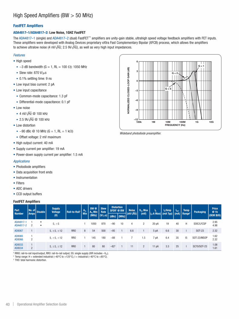
40 | Operational Amplifier Selection Guide
FastFET Amplifiers
Part Number
No. of Amps
DisableSupply Voltage
(V)Rail-to-Rail1 ACL
Min
BW @ ACL Min
(MHz)
Slew Rate
(V/ms)
Distortion SFDR1 @ BW Noise
(nV/√Hz)VOS Max
(mV)IB
(µA Max)IS/Amp
(mA Typ)IOUT
(mA)Temp
Range2 PackagingPrice @ 1k
(OEM $US)(dBc) (MHz)
ADA4817-1 ADA4817-2
1 2
• • 5, 65 1 1050 870 –90 10 4 2 20 pA 19 40 H SOIC/LFCSP
2.95 4.98
AD8067 1 5, 65, 612 RRO 8 54 500 –95 1 6.6 1 5 pA 6.6 30 I SOT-23 2.32
AD8065 AD8066
1 2 5, 65, 612 RRO 1 145 180 –88 1 7 1.5 7 pA 6.4 35 I5 SOT-23/MSOP
1.62 2.32
AD8033 AD8034
1 2 5, 65, 612 RRO 1 80 80 –823 1 11 2 11 pA 3.3 25 I SC70/SOT-23
1.08 1.61
1 RRIO: rail-to-rail input/output, RRO: rail-to-rail output, SS: single supply (IVR includes –VSY).2 Temp range: H = extended industrial (–40°C to +125°C), I = industrial (–40°C to +85°C).3 THD: total harmonic distortion.
High Speed Amplifiers (BW > 50 MHz)
FastFET Amplifiers
ADA4817–1/ADA4817–2: Low Noise, 1GHZ FastFET
The ADA4817–1 (single) and ADA4817–2 (dual) FastFET™ amplifiers are unity-gain stable, ultrahigh speed voltage feedback amplifiers with FET inputs. These amplifiers were developed with Analog Devices proprietary eXtra Fast Complementary Bipolar (XFCB) process, which allows the amplifiers to achieve ultralow noise (4 nV/√Hz; 2.5 fA/√Hz), as well as very high input impedances.
Features
•High speed
• −3 dB bandwidth (G = 1, RL = 100 V): 1050 MHz
• Slew rate: 870 V/ms
• 0.1% settling time: 9 ns
•Low input bias current: 2 pA
•Low input capacitance
• Common-mode capacitance: 1.3 pF
• Differential-mode capacitance: 0.1 pF
•Low noise
• 4 nV/√Hz @ 100 kHz
• 2.5 fA/√Hz @ 100 kHz
•Low distortion
• −90 dBc @ 10 MHz (G = 1, RL = 1 kV)
• Offset voltage: 2 mV maximum
•High output current: 40 mA
•Supply current per amplifier: 19 mA
•Power-down supply current per amplifier: 1.5 mA
Applications•Photodiode amplifiers
•Data acquisition front ends
• Instrumentation
•Filters
•ADC drivers
•CCD output buffers
Wideband photodiode preamplifier.
6
–12100k 10G
NO
RM
ALI
ZE
D C
LOS
ED
-LO
OP
GA
IN (d
B)
FREQUENCY (Hz)1M 10M 100M 1G
3
0
–3
–6
–9
G = 1
G = 2
G = 5

| 41www.analog.com/opamps
High Speed Amplifiers (BW > 50 MHz)
Current Feedback Amplifiers
AD8000: 1.5 GHz Ultrahigh Speed Op Amp
The AD8000 is an ultrahigh speed, high performance, current feedback amplifier. Using ADI’s proprietary eXtra Fast Complementary Bipolar (XFCB) process, the amplifier can achieve a small signal bandwidth of 1.5 GHz and a slew rate of 4100 V/ms.
Features
•High speed
• 1.5 GHz, −3 dB bandwidth (G = +1)
• 650 MHz, full power bandwidth (G = +2, VO = 2 V p-p)
• Slew rate: 4100 V/ms
• 0.1% settling time: 12 ns
• 0.1 dB flatness: 170 MHz
•Low noise: 1.6 nV/√Hz input voltage noise
•Low distortion over wide bandwidth
• 75 dBc SFDR @ 20 MHz
• 62 dBc SFDR @ 50 MHz
• Input offset voltage: 1 mV typ
•High output current: 100 mA
•Wide supply voltage range: 4.5 V to 12 V
•Supply current: 13.5 mA
Applications
•Professional video
•High speed instrumentation
•Video switching
• IF/RF gain stage
•CCD imaging
Large signal frequency response.
Current Feedback Amplifiers
Part Number
No. of Amps
DisableSupply Voltage
(V)Rail-to-Rail1 ACL
MIN
BW @ ACL MIN
(MHz)
Slew Rate
(V/ms)
Distortion SFDR1 @ BW Noise
(nV/√Hz)Noise3
(pa/√Hz)VOS Max
(mV)IB
(µA Max)IS/Amp
(mA Typ)IOUT
(mA)Temp
Range2 PackagingPrice @ 1k
(OEM $US)(dBc) (MHz)
ValueADA4860-1 1 • 5, 6 5 1 800 790 –75 10 4 1.5/7.7 13 10 6 85 I SOT-23 0.55
ADA4861-3 3 • 5, 6 5 1 730 680 –68 10 3.8 1.7/5.5 13 13 6 100 I SOIC 0.95
ADA4862-3 3 • 5, 6 5 2 500 1050 –68 10 10.6 (RTO) 1.4 25 (RTO) 1 5.5 75 I SOIC 0.95
AD8014 1 5, 6 5 1 480 4000 –70 5 3.5 5 5 15 1.1 50 I SOT-23/SOIC 1.19
AD8072 AD8073
2 3 5, 6 5 1 100 500 –64 5 3 6 6 12 3.5 30 I SOIC/MSOP
1.652.15
High PerformanceAD8000 AD8003
1 3
• • 5, 6 5 1 1500 4100 –75 20 1.6
3.4/26 3/36
10 45 13.5 100 H5 SOIC/LFCSP 1.68
AD8009 1 5, 6 5 1 1000 5500 –38 20 1.9 46/41 5 150 14 175 I SOT-23/SOIC 1.75
AD8001 AD8002
1 2 6 5 1 880 1000 –66 5 2 2/18 5.5 25 5 70 I SOT-23/SOIC 1.49
AD8007 AD8008
1 2 5, 6 5 1 650 1000 –83 20 2.7 2/23 4 8 9 30 I
SC70/SOT-23/ SOIC/MSOP
1.312.19
AD8011 1 5, 6 5 1 400 3500 –75 5 2 5 5 15 1 30 I SOIC 2.27
AD8023 3 • 5, 6 5 1 400 1200 –78 5 2 14 5 45 6.2 70 I SOIC 5.14
AD8005 1 5, 6 5 1 270 1500 –53 5 4 1.1/.9.1 30 10 0.4 10 I SOT-23 1.63
AD8004 4 5, 6 5 1 250 3000 –78 5 1.5 38 3.5 90 3.5 50 I SOIC 4.35
ADA4310-1 2 • 5, 6 5 2 190 820 –95 1 2.9 22 1 6 7.6 250 I LFCSP/MSOP 1.43
AD8017 2 5, 6 5 1 160 1600 –78 0.5 1.9 23/21 3 67 7 270 I SOIC 2.36
AD8013 3 • 5, 6 5 1 140 1000 –76 5 3.5 12 5 15 4 30 I SOIC 4.82
With Charge PumpADA4858-3 3 • 3, 5 1 600 600 –71 5 4 2/9 14 13 19 21 H LFCSP 1.69
ADA4859-3 3 • 3, 5 2 195 740 –70 5 17 (RTO) 2 25 (RTO) 2 17 19 H LFCSP 1.69 1 RRIO: rail-to-rail input/output, RRO: rail-to-rail output, SS: single supply (IVR includes –VSY).2 Temp range: H = extended industrial (–40°C to +125°C), I = industrial (–40°C to +85°C).3 Noise first entry is noninverting input, second entry is inverting input.
–7
–6
–5
–4
–3
–2
–1
0
1
2
3
NO
RM
ALI
ZE
D G
AIN
(dB
)
FREQUENCY (MHz)
1 10010 1000
VS = ±5VRL = 150VOUT = 2V p-p
G = +2, RF = 432
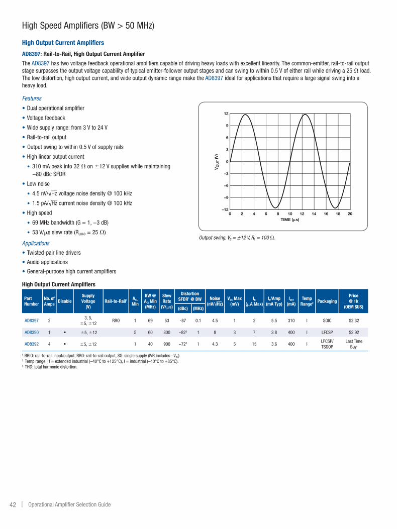
42 | Operational Amplifier Selection Guide
High Speed Amplifiers (BW > 50 MHz)
High Output Current Amplifiers
AD8397: Rail-to-Rail, High Output Current Amplifier
The AD8397 has two voltage feedback operational amplifiers capable of driving heavy loads with excellent linearity. The common-emitter, rail-to-rail output stage surpasses the output voltage capability of typical emitter-follower output stages and can swing to within 0.5 V of either rail while driving a 25 Ω load. The low distortion, high output current, and wide output dynamic range make the AD8397 ideal for applications that require a large signal swing into a heavy load.
Features
•Dual operational amplifier
•Voltage feedback
•Wide supply range: from 3 V to 24 V
•Rail-to-rail output
• Output swing to within 0.5 V of supply rails
•High linear output current
• 310 mA peak into 32 Ω on ±12 V supplies while maintaining −80 dBc SFDR
•Low noise
• 4.5 nV/√Hz voltage noise density @ 100 kHz
• 1.5 pA/√Hz current noise density @ 100 kHz
•High speed
• 69 MHz bandwidth (G = 1, −3 dB)
• 53 V/µs slew rate (RLOAD = 25 Ω)
Applications
•Twisted-pair line drivers
•Audio applications
•General-purpose high current amplifiers
Output swing, VS = ±12 V, RL = 100 Ω.
12
–12
–9
–6
–3
0
3
6
9
0 2 4 6 8 10 12 14 16 18 20TIME (s)
VO
UT (V
)
High Output Current Amplifiers
Part Number
No. of Amps
DisableSupply Voltage
(V)Rail-to-Rail1 ACL
Min
BW @ ACL Min
(MHz)
Slew Rate
(V/ms)
Distortion SFDR1 @ BW Noise
(nV/√Hz)VOS Max
(mV)IB
(µA Max)IS/Amp
(mA Typ)IOUT
(mA)Temp
Range2 PackagingPrice @ 1k
(OEM $US)(dBc) (MHz)
AD8397 23, 5,
65, 612RRO 1 69 53 -87 0.1 4.5 1 2 5.5 310 I SOIC $2.32
AD8390 1 • 65, 612 5 60 300 –823 1 8 3 7 3.8 400 I LFCSP $2.92
AD8392 4 • 65, 612 1 40 900 –723 1 4.3 5 15 3.6 400 ILFCSP/TSSOP
Last Time Buy
1 RRIO: rail-to-rail input/output, RRO: rail-to-rail output, SS: single supply (IVR includes –VSY).2 Temp range: H = extended industrial (–40°C to +125°C), I = industrial (–40°C to +85°C).3 THD: total harmonic distortion.
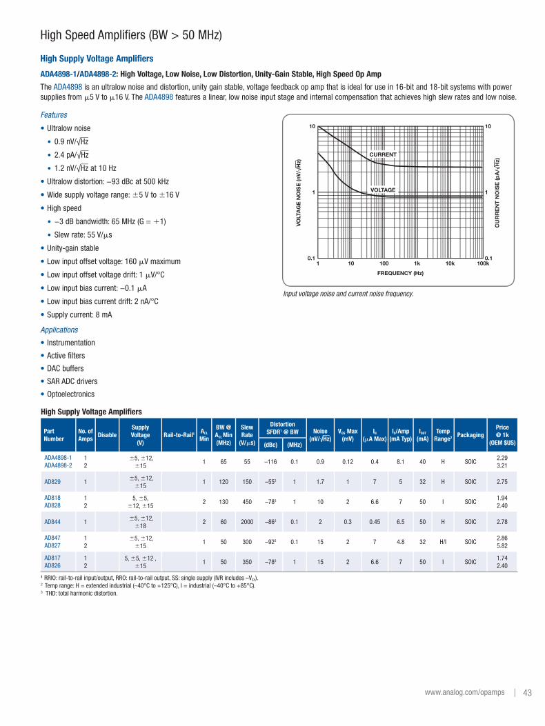
| 43www.analog.com/opamps
High Speed Amplifiers (BW > 50 MHz)
High Supply Voltage Amplifiers
ADA4898-1/ADA4898-2: High Voltage, Low Noise, Low Distortion, Unity-Gain Stable, High Speed Op Amp
The ADA4898 is an ultralow noise and distortion, unity gain stable, voltage feedback op amp that is ideal for use in 16-bit and 18-bit systems with power supplies from µ5 V to µ16 V. The ADA4898 features a linear, low noise input stage and internal compensation that achieves high slew rates and low noise.
Features
•Ultralow noise
• 0.9 nV/√Hz
• 2.4 pA/√Hz
• 1.2 nV/√Hz at 10 Hz
•Ultralow distortion: −93 dBc at 500 kHz
•Wide supply voltage range: ±5 V to ±16 V
•High speed
• −3 dB bandwidth: 65 MHz (G = +1)
• Slew rate: 55 V/µs
•Unity-gain stable
•Low input offset voltage: 160 µV maximum
•Low input offset voltage drift: 1 µV/°C
•Low input bias current: −0.1 µA
•Low input bias current drift: 2 nA/°C
•Supply current: 8 mA
Applications
• Instrumentation
•Active filters
•DAC buffers
•SAR ADC drivers
•Optoelectronics
High Supply Voltage Amplifiers
Part Number
No. of Amps
DisableSupply Voltage
(V)Rail-to-Rail1 ACL
Min
BW @ ACL Min
(MHz)
Slew Rate
(V/ms)
Distortion SFDR1 @ BW Noise
(nV/√Hz)VOS Max
(mV)IB
(µA Max)IS/Amp
(mA Typ)IOUT
(mA)Temp
Range2 PackagingPrice @ 1k
(OEM $US)(dBc) (MHz)
ADA4898-1 ADA4898-2
1 2
65, 612, 615
1 65 55 –116 0.1 0.9 0.12 0.4 8.1 40 H SOIC2.29 3.21
AD829 1 65, 612, 615
1 120 150 –553 1 1.7 1 7 5 32 H SOIC 2.75
AD818 AD828
1 2
5, 65, 612, 615
2 130 450 –783 1 10 2 6.6 7 50 I SOIC1.94 2.40
AD844 1 65, 612, 618
2 60 2000 –863 0.1 2 0.3 0.45 6.5 50 H SOIC 2.78
AD847 AD827
1 2
65, 612, 615
1 50 300 –923 0.1 15 2 7 4.8 32 H/I SOIC2.86 5.82
AD817 AD826
1 2
5, 65, 612 , 615
1 50 350 –783 1 15 2 6.6 7 50 I SOIC1.74 2.40
1 RRIO: rail-to-rail input/output, RRO: rail-to-rail output, SS: single supply (IVR includes –VSY).2 Temp range: H = extended industrial (–40°C to +125°C), I = industrial (–40°C to +85°C).3 THD: total harmonic distortion.
Input voltage noise and current noise frequency.
FREQUENCY (Hz)
VO
LTA
GE
NO
ISE
(nV
/√H
z)
CU
RR
EN
T N
OIS
E (p
A/√
Hz)
10.1
1
10
0.1
1
10
10 100 1k 10k 100k
CURRENT
VOLTAGE
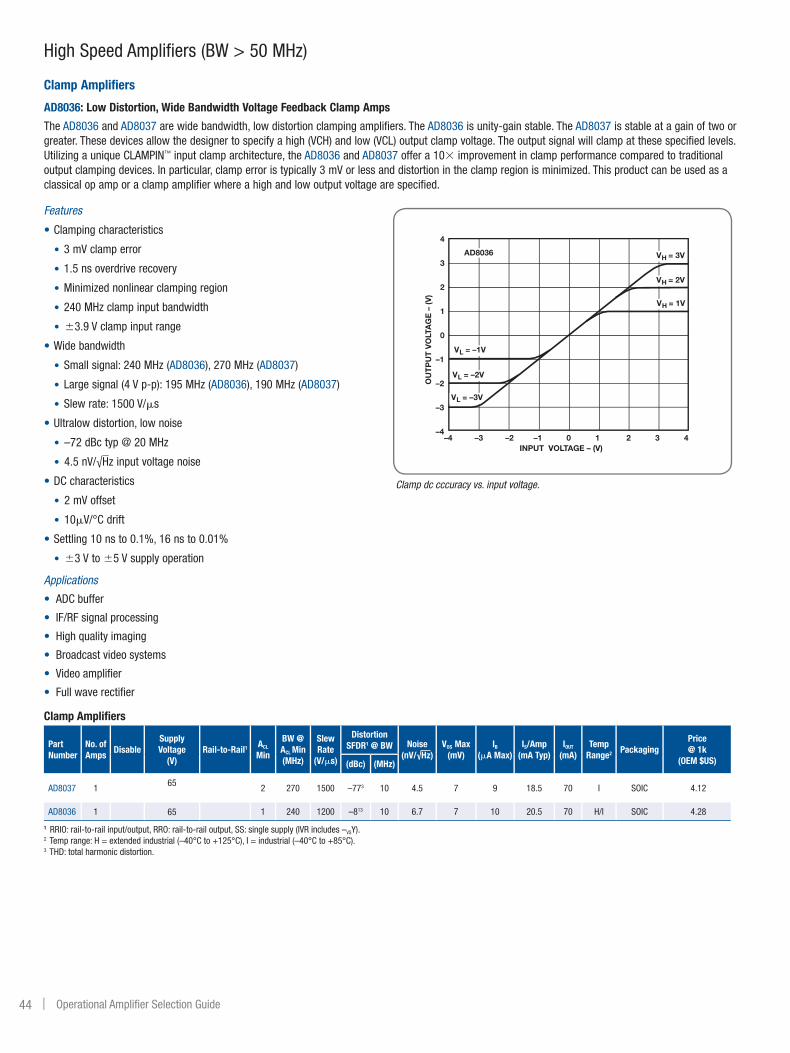
44 | Operational Amplifier Selection Guide
High Speed Amplifiers (BW > 50 MHz)
Clamp Amplifiers
AD8036: Low Distortion, Wide Bandwidth Voltage Feedback Clamp Amps
The AD8036 and AD8037 are wide bandwidth, low distortion clamping amplifiers. The AD8036 is unity-gain stable. The AD8037 is stable at a gain of two or greater. These devices allow the designer to specify a high (VCH) and low (VCL) output clamp voltage. The output signal will clamp at these specified levels. Utilizing a unique CLAMPIN™ input clamp architecture, the AD8036 and AD8037 offer a 10× improvement in clamp performance compared to traditional output clamping devices. In particular, clamp error is typically 3 mV or less and distortion in the clamp region is minimized. This product can be used as a classical op amp or a clamp amplifier where a high and low output voltage are specified.
Features
•Clamping characteristics
• 3 mV clamp error
• 1.5 ns overdrive recovery
•Minimized nonlinear clamping region
• 240 MHz clamp input bandwidth
• ±3.9 V clamp input range
•Wide bandwidth
• Small signal: 240 MHz (AD8036), 270 MHz (AD8037)
• Large signal (4 V p-p): 195 MHz (AD8036), 190 MHz (AD8037)
• Slew rate: 1500 V/µs
•Ultralow distortion, low noise
• –72 dBc typ @ 20 MHz
• 4.5 nV/√Hz input voltage noise
•DC characteristics
• 2 mV offset
• 10µV/°C drift
•Settling 10 ns to 0.1%, 16 ns to 0.01%
• ±3 V to ±5 V supply operation
Applications
• ADC buffer
• IF/RF signal processing
• High quality imaging
• Broadcast video systems
• Video amplifier
• Full wave rectifier
Clamp Amplifiers
Part Number
No. of Amps
DisableSupply Voltage
(V)Rail-to-Rail1 ACL
Min
BW @ ACL Min
(MHz)
Slew Rate
(V/ms)
Distortion SFDR1 @ BW Noise
(nV/√Hz)VOS Max
(mV)IB
(µA Max)IS/Amp
(mA Typ)IOUT
(mA)Temp
Range2 PackagingPrice @ 1k
(OEM $US)(dBc) (MHz)
AD8037 1 65 2 270 1500 –773 10 4.5 7 9 18.5 70 I SOIC 4.12
AD8036 1 65 1 240 1200 –813 10 6.7 7 10 20.5 70 H/I SOIC 4.28
1 RRIO: rail-to-rail input/output, RRO: rail-to-rail output, SS: single supply (IVR includes –VSY).2 Temp range: H = extended industrial (–40°C to +125°C), I = industrial (–40°C to +85°C).3 THD: total harmonic distortion.
Clamp dc cccuracy vs. input voltage.
–4 –3 –2 –1 0 1 2 3 4
4
3
2
1
0
–1
–2
–3
–4
INPUT VOLTAGE – (V)
OU
TP
UT
VO
LTA
GE
– (V
)
VL = –3V
VL = –2V
VL = –1V
VH = 1V
VH = 2V
VH = 3VAD8036

| 45www.analog.com/opamps
Analog Devices has been developing innovative energy solutions for over a decade. Our portfolio of high performance amplifiers plays a key role in advancing power quality monitoring in substation equipment and, more recently, enables breakthrough solutions in renewable energy systems.
Amplifiers for Energy Applications
Application Recommended Amplifiers Key Amplifier Characteristics
Renewable energy generation—wind turbinesPrecision: OP282, AD820, AD822, AD824, OP4177,
OP2177, AD8622, AD8624Low noise, high load drive
Renewable energy generation—solar invertersPrecision: AD8512, AD824, ADA4610-2
High speed: AD8039, AD8092Low noise, low input bias current
low power, low cost
Substation automation—transmission and distributionPrecision: AD8510, AD8512, AD8513,
OP4177, AD8622, AD8624Low noise, low input bias current
AMP
AMP
PT
CT
OTHERINPUTS
DSP PROCESSOR
POWER MANAGEMENT
SIGNALCONDITIONING
AMP
VOLTAGEREFERENCE
GALVANICISOLATIONBARRIER
MULTICHANNELSIMULTANEOUSSAMPLING ADC
PWMDRIVER
DSP
ISOLATION
DC-TO-DC DC-TO-AC
STRINGOF PV
PANELS FILTER
AMP
AMP AMP
AMP
AMP
CANDRIVERCAN
PWMDRIVER
For more information in energy applications, visit energy.analog.com.
Typical substation automation system diagram.
Typical solar cell system diagram.

46 | Operational Amplifier Selection Guide
Amplifiers for Applications in Process Control and Industrial Automation
For over 40 years, designers of industrial process control systems and Analog Devices have worked together to define, develop, and deploy complete signal chain solutions, optimized for a wide array of applications. We bring reliability and innovation to this process with precision control and monitoring solutions based on our industry-leading technologies and systems-level expertise.
ApplicationRecommended Amplifiers
for Input StageRecommended Amplifiers
for Output StageKey Amplifier Characteristics
Programmable logic controllers (PLC)/ distribution contol systems (DCS)
Precision: OP2177, OP177, OP07, ADA4091-2, AD8677, OP213, OP295, OP284, AD822, ADA4091, ADA4092, ADA4051-2, AD8629, AD8639, AD8572,
AD8539, AD8607, AD8606, AD8542, ADA4692, AD8617, AD8657
Precision: AD8622, AD822, OP297, ADTL082, AD8607, AD8606, AD8542, ADA4692, AD8617,
AD8657, OP2177, OP177, OP07, ADA4091, AD8677, ADA4062, ADA4692
Precision, low power, overvoltage protection, high voltage
High speed: AD8021, AD8051, AD8032, AD8029, AD8062, AD8099, AD8045, ADA4899-1,
ADA4899-2, ADA4898-1, AD4898-2, AD8139, ADA4927, ADA4940
High speed: AD8397, ADA4891-1, ADA4891-2, ADA4891-3, ADA4891-4, AD8017
High speed, low noise, high output current
Field instrumentation and smart transmitters
Precision: AD8538, AD8628, OP4177Precision: AD8655, AD8656, AD8615,
AD8616, AD8618Precision, low power
MUX
MUX
VO
UT
_1
VO
UT
_2
VO
UT
_3
VO
UT
_N
POWERREGULATORSPWR IN
ACTUATOR CONTROL/ VALVE CONTROL
4mA TO 20mA COMMS
SENSOR AMP
AMP
AMP
TEMPERATURE
FLOW
PRESSURE
ADC ISOLATION
SENSOR
DAC ISOLATION SYSTEMINTERFACE
SYSTEM CONTROLLER/PROCESSOR
REF
REF
AMP/DRIVER
BUFFER
BUFFER
For more information in process control and industrial automation applications, visit processcontrol.analog.com.
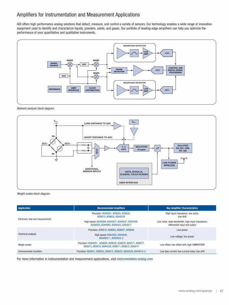
| 47www.analog.com/opamps
Application Recommended Amplifiers Key Amplifier Characteristics
Electronic test and measurement
Precision: ADA4051, AD8655, AD8656, AD8615, AD8605, ADA4528
High input impedance, low noise, low drift
High speed: ADA4899, ADA4927, ADA4937, ADA4938, ADA4939, ADA4960, ADA4932, ADA4817
Low noise, wide bandwidth, high input impedance, differential input and output
Chemical analysis
Precision: AD8616, AD8603, AD8607, AD8609 Low power
High speed: ADA4930, ADA4940, ADA4932-1, ADA4932-2
Low voltage, low power
Weigh scalesPrecision: ADA4051, AD8628, AD8638, AD8639, AD8571, AD8677,
AD8675, AD8676, ADA4528, AD8671, AD8672, AD8674Low offset; low offset drift, high CMRR/PSRR
Environmental monitors Precision: AD8657, AD8655, AD8615, AD8622, ADA4528, ADA4610-2 Low bias current, low current noise, low drift
Amplifiers for Instrumentation and Measurement Applications
ADI offers high performance analog solutions that detect, measure, and control a variety of sensors. Our technology enables a wide range of innovative equipment used to identify and characterize liquids, powders, solids, and gases. Our portfolio of leading-edge amplifiers can help you optimize the performance of your quantitative and qualitative instruments.
MIXER MIXER
MIXER
REFERENCEUSER
INTERFACECLOCK
DISTRIBUTION
SIGNALSOURCE DUT
VCO
ADCLOGAMP
MAGNITUDE DETECTOR
ADCLOGAMP
MAGNITUDE DETECTOR
PHASEDETECTOR
ADCCONTROL AND
DIGITAL SIGNAL PROCESSING
Weight scales block diagram.
OUT–
IN+
IN–
OUT+
LONG DISTANCE TO ADC
SHORT DISTANCE TO ADC
VEXC
KEYS, SCROLLS,SLIDERS, TOUCH SCREEN
ISOLATEDRS-232, USB,
RS-485
USER INTERFACE
LOW POWERWIRELESS
ISOLATIONiCoupler
P-
ADC
MU
X
ADDITIONALSENSOR INPUTS
VREF
Network analyzer block diagram.
For more information in instrumentation and measurement applications, visit instrumentation.analog.com.

48 | Operational Amplifier Selection Guide
Amplifiers for Motor and Power Control Applications
Application Recommended Amplifiers Key Amplifier Characteristics
Motor controlADA4051, AD8657, AD8512, AD8620, AD8622, AD8624, OP1177, OP2177, OP4177, AD8510, AD8513, AD8602,
AD8604, ADA4000, ADA4096, ADA4528Low noise, low offset voltage, low offset drift
Analog Devices offers a complete product portfolio to optimize system-level and applications-oriented designs for motor and power control solutions. ADI’s amplifier products provide many advantages in current sensing and voltage sensing applications.
SYSTEM CONTROLINTERFACE MOTOR CONTROL
IC-DSP
ISOLATIONISOLATION
GATE DRIVEDEVICES
IGBTPOWER MOTOR
ISOLATION ISOLATION ADC
POWER FEEDBACKOR
RESOLVER/DIG
I-SENSEAMP
For more information in motor and power control applications, visit motorcontrol.analog.com.
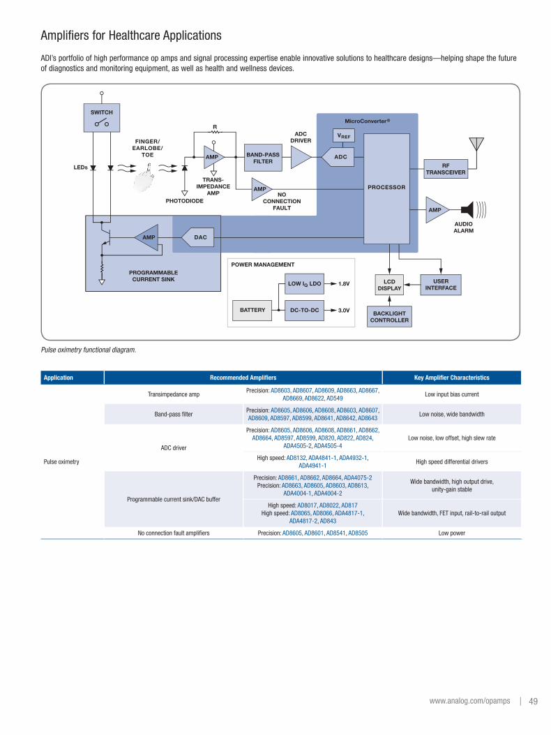
| 49www.analog.com/opamps
Amplifiers for Healthcare Applications
Pulse oximetry functional diagram.
FINGER/EARLOBE/
TOE
AMP
LEDs
SWITCH
ADCDRIVER
NOCONNECTION
FAULT
PROGRAMMABLECURRENT SINK
DAC
ADCAMP
R
TRANS-IMPEDANCE
AMPPHOTODIODE
AMP
POWER MANAGEMENT
1.8V
3.0VBATTERY DC-TO-DC
AUDIOALARM
AMP
MicroConverter®
USERINTERFACE
LCDDISPLAY
BACKLIGHTCONTROLLER
LOW IQ LDO
PROCESSOR
RFTRANSCEIVER
BAND-PASSFILTER
VREF
ADI’s portfolio of high performance op amps and signal processing expertise enable innovative solutions to healthcare designs—helping shape the future of diagnostics and monitoring equipment, as well as health and wellness devices.
Application Recommended Amplifiers Key Amplifier Characteristics
Pulse oximetry
Transimpedance ampPrecision: AD8603, AD8607, AD8609, AD8663, AD8667,
AD8669, AD8622, AD549Low input bias current
Band-pass filterPrecision: AD8605, AD8606, AD8608, AD8603, AD8607, AD8609, AD8597, AD8599, AD8641, AD8642, AD8643
Low noise, wide bandwidth
ADC driver
Precision: AD8605, AD8606, AD8608, AD8661, AD8662, AD8664, AD8597, AD8599, AD820, AD822, AD824,
ADA4505-2, ADA4505-4Low noise, low offset, high slew rate
High speed: AD8132, ADA4841-1, ADA4932-1, ADA4941-1
High speed differential drivers
Programmable current sink/DAC buffer
Precision: AD8661, AD8662, AD8664, ADA4075-2Precision: AD8663, AD8605, AD8603, AD8613,
ADA4004-1, ADA4004-2
Wide bandwidth, high output drive, unity-gain stable
High speed: AD8017, AD8022, AD817High speed: AD8065, AD8066, ADA4817-1,
ADA4817-2, AD843Wide bandwidth, FET input, rail-to-rail output
No connection fault amplifiers Precision: AD8605, AD8601, AD8541, AD8505 Low power

50 | Operational Amplifier Selection Guide
Ultrasound functional diagram.
AMP
VGALNA
AMP/FILTER
ADC
ADC
ADC
AUDIODAC
IMAGE ANDMOTION
PROCESSING(B MODE)
CLOCKS
LNA-VGA-ADC ARRAY (UP TO 256 CHANNELS)
COLORDOPPLER
PROCESSING(F MODE)
VIDEO DAC/VIDEO ENCODER
VIDEOCOMPRESSION
CWDOPPLER
PROCESSING
I/QPROCESSING
T/RSWITCHER
HV MUX ANDT/R SWITCHES
BEAMFORMERCENTRAL CONTROL
PROCESSOR
DVR
HVAMP DAC ISOLATION
ADI INTEGRATED SOLUTION
DIGITAL RxBEAMFORMER
AAF
AMP
AMP
TRANSDUCERARRAY
Instrumentation/blood analysis using flow cytometry
Transimpedance ampPrecision: AD8603, AD8607, AD8609, AD8610, AD8620, AD8663,
AD8667, AD8669, AD8622, AD549 , ADA4051, ADA4627, ADA4610Low input bias current
DAC bufferPrecision: AD8605, AD8606, AD8608, AD8661, AD8662,
AD8664, ADA4075-2High bandwidth, high output drive
Photodiode pre-amp
High speed: AD8033, AD8034, AD8065, AD8066, AD8067, AD8610, AD8615, AD8618, AD8620, ADA4817-1, ADA4817-2
High speed, FET input
High speed: AD8022, AD8029, AD8041, AD812, AD818, ADA4851-1, ADA4851-2
Wide bandwidth, low noise, rail-to-rail, low power
ADC driverHigh speed: ADA4941-1, ADA4932-1, ADA4932-2, ADA4940-1,
ADA4940-2, ADA4950-1, ADA4950-2, AD8138, AD8137Low noise, low offset, high slew rate
HRM (heart rate monitoring devices)/blood pressure monitor
Band-pass filterPrecision: AD8500, ADA4051-1, ADA4051-2, AD8603, AD8607,
AD8609, AD8508, AD8541, AD8538, AD8539, AD8642, ADA4505, AD8655, AD8656, ADA4505-4
Low noise, low power, wide bandwidth
Audio ampPrecision: AD8691, AD8692, AD8694, AD8665, ADA4665-2,
AD8668, ADA4075-2Low noise, high output drive
ADC driver High speed: ADA4941, ADA4940 Low noise, low offset, high slew rate
Application Recommended Amplifiers Key Amplifier Characteristics
Ultrasound
Dual channel, low noise
High speed: AD810, AD812, AD813, AD815, AD817, AD825, AD826, AD818, AD827, AD828, AD829, AD847, AD4898-1, AD4898-2, OP467
High voltage, wide bandwidth
High speed: ADA4841-1, ADA4898-1, ADA4899-1, AD8012, AD8021, AD8022, AD8099 Low noise, high speed
Amplifiers for Healthcare Applications (continued)
For more information in healthcare applications, visit healthcare.analog.com.
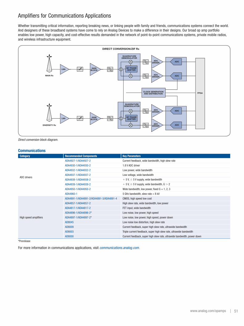
| 51www.analog.com/opamps
Amplifiers for Communications Applications
Direct conversion block diagram.
MAIN Rx
DIRECT CONVERSION/ZIF Rx
DIVERSITY Rx
ADC
ADC
LNA
QUADRATUREDEMODULATOR
ADC
ADC
LNA
QUADRATUREDEMODULATOR
GAINBLOCK
GAINBLOCK
ADCDRIVER
ADCDRIVER
ADCDRIVER
ADCDRIVER
CLOCK GENERATIONAND DISTRIBUTION FPGA
90 PHASESHIFTER
º
90 PHASESHIFTER
º
CommunicationsCategory Recommended Components Key Parameters
ADC drivers
ADA4927-1/ADA4927-2 Current feedback, wide bandwidth, high slew rate
ADA4930-1/ADA4930-2 1.8 V ADC driver
ADA4932-1/ADA4932-2 Low power, wide bandwidth
ADA4937-1/ADA4937-2 Low voltage, wide bandwidth
ADA4938-1/ADA4938-2 + 5 V, ± 5 V supply, wide bandwidth
ADA4939-1/ADA4939-2 + 5 V, ± 5 V supply, wide bandwidth, G > 2
ADA4950-1/ADA4950-2 Wide bandwidth, low power, fixed G = 1, 2, 3
ADA4960-1 5 GHz bandwidth, slew rate = 8 kV
High speed amplifiers
ADA4891-1/ADA4891-2/ADA4891-3/ADA4891-4 CMOS, high speed low cost
ADA4857-1/ADA4857-2 High slew rate, wide bandwidth, low power
ADA4817-1/ADA4817-2 FET input, wide bandwidth
ADA4896-1/ADA4896-2* Low noise, low power, high speed
ADA4897-1/ADA4897-2* Low noise, low power, high speed, power down
AD8045 Low noise low distortion, high slew rate
AD8009 Current feedback, super high slew rate, ultrawide bandwidth
AD8003 Triple current feedback, super high slew rate, ultrawide bandwidth
AD8000 Current feedback, super high slew rate, ultrawide bandwidth, power down
*Prerelease
For more information in communications applications, visit communications.analog.com.
Whether transmitting critical information, reporting breaking news, or linking people with family and friends, communications systems connect the world. And designers of these broadband systems have come to rely on Analog Devices to make a difference in their designs. Our broad op amp portfolio enables low power, high capacity, and cost-effective results demanded in the network of point-to-point communications systems, private mobile radios, and wireless infrastructure equipment.

52 | Operational Amplifier Selection Guide
Amplifiers for Consumer Audio Applications
Application Recommended Amplifiers Key Amplifier Characteristics
Audio pre-amps AD8597, AD8599, AD797 Low noise
Microphone pre-amps
ADA4004 Low distortion
AD8510, AD8512, AD8513 Low power
AD8627, AD8646, AD8647, AD8648, AD8691, AD8692, AD8694, ADA4075, ADA4692
Low cost
AUDIOAMP
AUDIONOISEGATE
AUDIOAMP
AUDIONOISEGATE
AUDIOVCA
AUDIOSWITCH
STEREODAC
AUDIOAMP
AUDIOAMP
AUDIOPROCESSOR
AUDIOLINE
DRIVER
AUDIOLINERCVR
STEREOADC
CLOCKS
For more information in consumer applications, visit consumer.analog.com.

| 53www.analog.com/opamps
Amplifiers for Automotive Applications
Application Recommended Amplifiers Part Description Key Amplifier Characteristics
Automotive sensing
Precision: AD8601WARTZ-R7, AD8601WARTZ-RL, AD8601WDRTZ-REEL
DigiTrim rail-to-rail input and output single amplifier with very low offset voltage
Auto-zero, low offset voltage and low offset voltage
Precision: AD8617WARMZ-REEL, AD8617WARZ-R7, AD8617WARZ-RL
Low cost, micropower, low noise, CMOS, rail-to-rail input/output op amp
Precision: AD8628WARTZ-R7, AD8628WARTZ-RL, AD8628WARZ-R7, AD8628WARZ-RL, AD8628WAUJZ-R7,
AD8628WAUJZ-RL
Zero drift, single-supply, rail-to-rail input/ output operational amplifier
Precision: AD8629WARZ-R7, AD8629WARZ-RLZero drift, single-supply, rail-to-rail, input/
output operational amplifier
Precision: AD8630WARZ-R7, AD8630WARZ-RLQuad, zero drift, single-supply, rail-to-rail operational amplifier
Precision: AD8646WARMZ-R7, AD8646WARMZ-RL, AD8646WARZ-R7, AD8646WARZ-RL
24 MHz, rail-to-rail, dual amplifier
Precision: AD8648WARUZ, AD8648WARUZ-RL 24 MHz, rail-to-rail, quad amplifier
Precision: AD8656WARMZ-REEL Low noise, precision CMOS dual amplifier
Infortainment and vision ADAS
High speed: ADA4851-1WYRJZ-R7, ADA4851-2WYRMZ-R7, ADA4851-4WYRUZ-R7
Low cost, rail-to-rail output op amp
Video amplifiersHigh speed: ADA4853-3WYRUZ-R7 Ultralow power, rail-to-rail output op amp
High speed: ADA4891-1WARJZ-R7, ADA4891-2WARMZ-R7, ADA4891-4WARUZ-R7
Low cost, CMOS, rail-to-rail op amp
Low cost
Advanced driver assistance (ADAS)
High speed: AD8040WARUZ-R7, AD8028WARMZ-R7, AD8065WARTZ-R7
Rail-to-rail, FET input Wide bandwidth, low power
High speed: AD8132WARMZ-R7, AD8137WYCPZ-R7 Single ended input or differential input, differential output Differential amps
Pressure sensingIn antilock brakingsystems (ABS)
Precision: AD8628WARTZ-R7, AD8628WARTZ-RL, AD8628WARZ-R7, AD8628WARZ-RL, AD8628WAUJZ-R7,
AD8628WAUJZ-RL
Zero-drift, single-supply, rail-to-rail input/ output operational amplifier
Low offset, low noise
Precision: AD8629WARZ-R7, AD8629WARZ-RLZero-drift, single-supply, rail-to-rail, input/
output operational amplifier
Precision: AD8630WARZ-R7, AD8630WARZ-RLQuad, zero-drift, single-supply, rail-to-rail
operational amplifier
Precision: AD8601WARTZ-R7, AD8601WARTZ-RL, AD8601WDRTZ-REEL
DigiTrim rail-to-rail input and output single amplifier with very low offset voltage
Precision: AD8692WARMZ-REELDual, low cost, low noise, CMOS rail-to-rail output
operational amplifier
Precision: AD8694WARUZ, AD8694WARUZ-REELQuad, low cost, low noise, CMOS rail-to-rail output
operational amplifier
With over 45 years of experience in signal processing and the industry’s leading portfolio, ADI provides design engineers with the robust amplifier products and technical support to build any automotive applications. ADI’s technologies are used to address the most challenging signal chain requirements in advanced safety, infotainment, power-train, and body/chassis electronics systems for electric, hybrid, and fossil fuel powered vehicles worldwide.
ADI’s automotive grade amplifiers are identified by the “W” suffix immediately after the part number. These products are qualified for automotive applications and meet or exceed the rigorous requirements of the automotive industry.
AIRBAG SYSTEMS
AUDIO SYSTEMS
ENGINE MANAGEMENT
SECURITY SYSTEMS
TIRE PRESSURE
ELECTRONIC POWER STEERING
ELECTRO HYDRAULIC BRAKES
BATTERY MANAGEMENT
ADAPTIVE SUSPENSION
TRANSMISSION
RADAR FORDRIVER ASSISTANCE
For more information in automotive applications, visit automotive.analog.com.

54 | Operational Amplifier Selection Guide
Amplifiers for Applications in Defense and Aerospace
For over 45 years Analog Devices has been at the forefront of innovation in signal processing for aerospace and defense applications. ADI’s commitment to performance and reliability has made ADI a preferred supplier to the Department of Defense and other U.S. and foreign defense agencies around the world. Today’s advanced defense systems in radar, communications, avionics, defense electronics, and much more demand the best in system level performance. ADI’s superior products and system level knowledge will help you overcome the most difficult of design challenges.
Precision High Speed
Part Number Model Number Description Part Number Model Number Description
OP115962-89801012A 5962-8980101CA
Quad matched 741-Type op amp AD830 5962-9313001MPA Video difference amp
OP27OP27AJ/883C OP27AZ/883C
Low noise, Precision op amp AD713 5962-9063301MCAQuad precision, low cost,
BiFET op amp
OP775962-87738012A 5962-8773802GA 5962-8773802PA
Ultralow offset voltage op amp AD8001 5962-9459301MPA800 MHz, 50 mW current
feedback amplifier
OP4005962-8777101M3A 5962-8777101MCA
Quad low offset, low power op amp
AD8004 AD8004SQ Quad 3000 V/µs, 35 mW current feedback amplifier
AD712 AD712SQ/883BPrecision, low cost, high speed,
BiFET dual op ampAD8036 5962-9559701MPA
Unity gain stable, low distortion, wide bandwidth voltage feedback clamp
amps
OP4705962-88565012A 5962-8856501CA
Very low noise, quad op amp AD8041 5962-9683901MPA160 MHz rail-to-rail amplifier
with disable
OP270 5962-8872101PA Very low noise dual op amp AD810 5962-9313201MPALow power video op amp
with disable
OP4715962-88565022A 5962-88565023A 5962-8856502CA
High speed, low noise quad op amp
AD811
5962-9313101M2A 5962-9313101MPA
AD811SCHIPS AD811SE/883B AD811SQ/883B
High performance video op amp
AD549 AD549SH/883B Ultralow input-bias current op amp AD813 5962-9559601M2ASingle supply, low power triple video
amplifier
OP2005962-8859301MPA 5962-8859301M2A
Dual low offset, low power operational amplifier
AD827
5962-9211701M2A 5962-9313101MPA
AD827SCHIPS AD827SE/883B
AD827SQ AD827SQ/883B
High performance video op amp
AMPDAC PA
ADCDRIVER
MIXER MIXER
MIXER MIXER
REFCLK
PLL
DDSFREQUENCYMULTIPLIER
CHAIN
MOTORCONTROL
LOG AMPDETECTORS
VIDEOPROCESSING DISPLAY
FPG
AR
AD
AR
SIG
NA
L P
RO
CE
SS
ING
AN
D C
ON
TR
OL
ADC LNARF/IFAMP
RF/IFAMP
RF/IFAMP
Defense Qualified Products
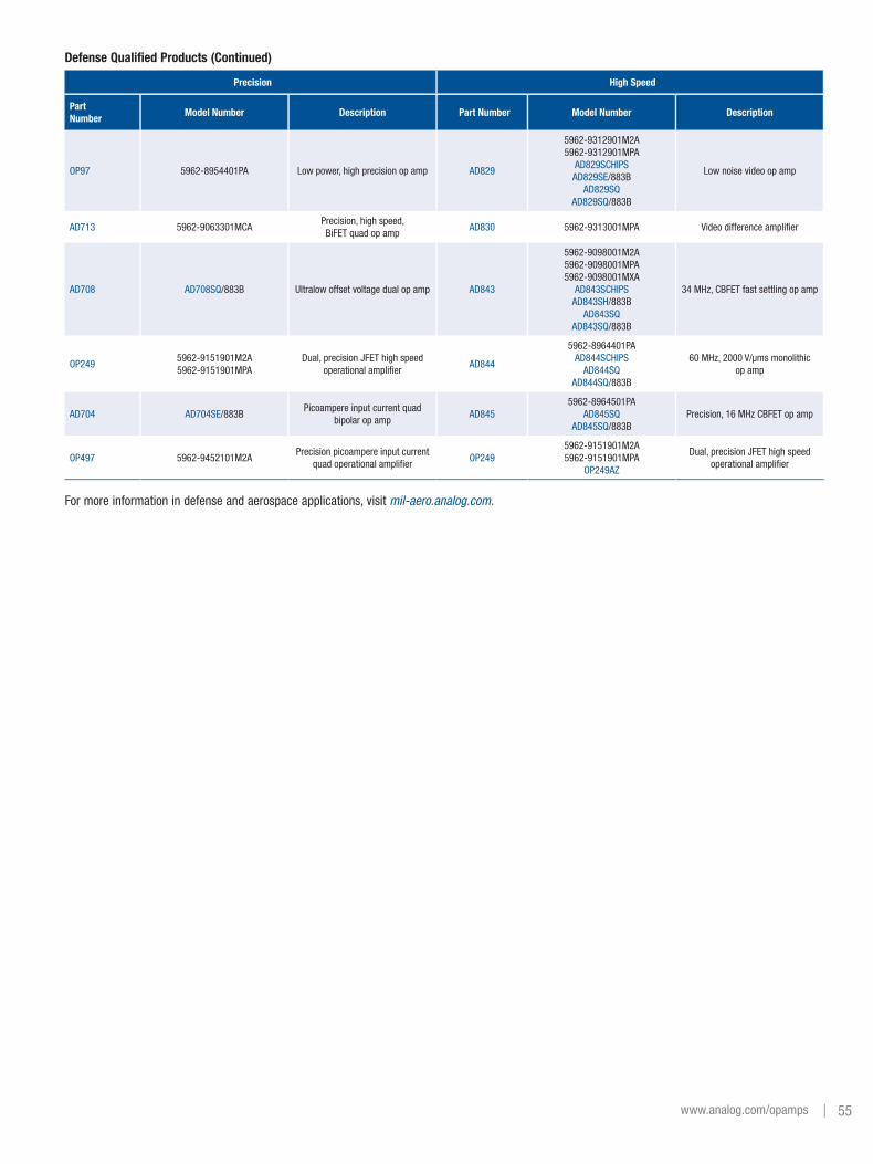
| 55www.analog.com/opamps
Precision High Speed
Part Number
Model Number Description Part Number Model Number Description
OP97 5962-8954401PA Low power, high precision op amp AD829
5962-9312901M2A 5962-9312901MPA
AD829SCHIPS AD829SE/883B
AD829SQ AD829SQ/883B
Low noise video op amp
AD713 5962-9063301MCAPrecision, high speed, BiFET quad op amp
AD830 5962-9313001MPA Video difference amplifier
AD708 AD708SQ/883B Ultralow offset voltage dual op amp AD843
5962-9098001M2A 5962-9098001MPA 5962-9098001MXA
AD843SCHIPS AD843SH/883B
AD843SQ AD843SQ/883B
34 MHz, CBFET fast settling op amp
OP2495962-9151901M2A 5962-9151901MPA
Dual, precision JFET high speed operational amplifier
AD844
5962-8964401PA AD844SCHIPS
AD844SQ AD844SQ/883B
60 MHz, 2000 V/μms monolithic op amp
AD704 AD704SE/883BPicoampere input current quad
bipolar op ampAD845
5962-8964501PA AD845SQ
AD845SQ/883BPrecision, 16 MHz CBFET op amp
OP497 5962-9452101M2APrecision picoampere input current
quad operational amplifierOP249
5962-9151901M2A 5962-9151901MPA
OP249AZ
Dual, precision JFET high speed operational amplifier
Defense Qualified Products (Continued)
For more information in defense and aerospace applications, visit mil-aero.analog.com.

56 | Operational Amplifier Selection Guide
Precision Op AmpsPart Number Model Number Package Description
Low Offset
AD8629S AD8629D703L 10-lead FP Zero-drift, single-supply, rail-to-rail input/output op amp
AD8671S 5962L0922301VHA 10-lead FP Single, very low noise, low input bias current op amp
OP07S
5962R9863901VGA 5962R9863901VHA 5962R9863901VPA
OP07000C OP07R000C
8-lead can 10-lead FP 8-lead DIP Class K die Class K die
Ultralow offset voltage op amp
OP22S OP220903J 8-lead can Programmable micropower op amp
OP27S
5962R9468002VGA 5962R9468002VHA 5962R9468002V2A 5962R9468002VPA
OP484-000COP484R000C
8-lead can 10-lead FP
20-lead LCC 8-lead DIP Class K die Class K die
Low noise precision op amp
OP37S5962-8853701VGA 5962-8853701VPA
8-lead can 8-lead DIP
Low noise precision high speed op amp
OP77S
5962-8773802VGA 5962-8773802VHA 5962-8773802V2A 5962-8773802VPA
8-lead can 10-lead FP
20-lead LCC 8-lead DIP
Ultralow offset voltage operational amplifier
OP200S5962-8859301V2A 5962-8859301VPA
20-lead LCC 8-lead DIP
Dual low offset, low power op amp
OP207S 5962R0821401VCA 14-lead DIP Dual ultralow VOS matched op amp
OP227SOP227R903Y OP227R903M
14-lead DIP 14-lead FP
Dual low noise low offset instrumentation op amp
OP270S
5962-8872101VPA 5962-8872101VDA 5962-8872101V2A 5962R8872101VPA 5962R8872101VDA 5962R8872101V2A
OP2700000C OP270R000C
8-lead DIP 14-lead FP
20-lead LCC 8-lead DIP 14-lead FP
20-lead LCC Class K die Class K die
Dual very low noise precision op amp
OP400S
5962-8777101VKA 5962-8777101V3A 5962-8777101VCA
OP400-000C
24-lead FP 28-lead LCC 14-lead DIP Class K die
Quad low offset, low power op amp
OP484S
5962-0051701VCA 5962-0051701VDA 5962R0051701VCA 5962R0051701VDA
OP484-000COP484R000C
14-lead DIP 14-lead FP 14-lead DIP 14-lead FP Class K die Class K die
Rail-to-rail input and output op amp
Low Input Bias
AD648S
5962-9753501VGA 5962-9753501VPA 5962-9753502VGA 5962-9753502VPA
6-lead can 8-lead DIP 6-lead can 8-lead DIP
Dual low power BiFET op amp
OP12SOP120903JOP120000C
8-lead can Class K die
Precision low input current operational amplifier
OP15S5962R8954203VGA 5962R8954203VHA 5962R8954203VPA
6-lead can 10-lead FP 8-lead DIP
Precision JFET input op amp
OP16S5962R8954304VGA 5962R8954304VPA
6-lead can 8-lead DIP
Precision JFET input op amp
OP42S5962-8851301VGA 5962-8851301VPA
6-lead can 8-lead DIP
OP215S
5962-8853801VGA 5962-8853801VPA 5962R8853801VGA 5962R8853801VPA 5962R8853804V2A
OP215-000C OP215R000C
6-lead can 8-lead DIP 6-lead can 8-lead DIP
20-lead LCC Class K die Class K die
Dual precision JFET input op amp
Space Qualified Products
Analog Devices is committed to serving the needs of the world space community by providing the highest quality linear and mixed-signal products. In addition to the comprehensive offering of amplifier products indentified below, ADI offers a broad range of other linear and data conversion device types for space applications. Analog Devices processes its space products to the highest quality levels of MIL-PRF-38535 QML Level V, including radiation hardness assurance (RHA) testing.
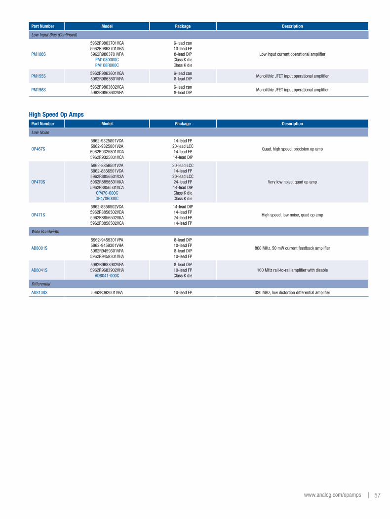
| 57www.analog.com/opamps
High Speed Op AmpsPart Number Model Package Description
Low Noise
OP467S
5962-9325801VCA 5962-9325801V2A 5962R9325801VDA 5962R9325801VCA
14-lead FP 20-lead LCC 14-lead FP 14-lead DIP
Quad, high speed, precision op amp
OP470S
5962-8856501V2A 5962-8856501VCA 5962R8856501V2A 5962R8856501VKA 5962R8856501VCA
OP470-000C OP470R000C
20-lead LCC 14-lead FP
20-lead LCC 24-lead FP 14-lead DIP Class K die Class K die
Very low noise, quad op amp
OP471S
5962-8856502VCA5962R8856502VDA5962R8856502VKA5962R8856502VCA
14-lead DIP 14-lead FP 24-lead FP 14-lead FP
High speed, low noise, quad op amp
Wide Bandwidth
AD8001S
5962-9459301VPA 5962-9459301VHA 5962R9459301VPA 5962R9459301VHA
8-lead DIP 10-lead FP 8-lead DIP 10-lead FP
800 MHz, 50 mW current feedback amplifier
AD8041S5962R9683902VPA 5962R9683902VHA
AD8041-000C
8-lead DIP 10-lead FP Class K die
160 MHz rail-to-rail amplifier with disable
Differential
AD8138S 5962R092001VHA 10-lead FP 320 MHz, low distortion differential amplifier
Part Number Model Package Description
Low Input Bias (Continued)
PM108S
5962R9863701VGA 5962R9863701VHA5962R9863701VPA
PM1080000CPM108R000C
6-lead can 10-lead FP 8-lead DIP Class K die Class K die
Low input current operational amplifier
PM155S5962R9863601VGA 5962R9863601VPA
6-lead can 8-lead DIP
Monolithic JFET input operational amplifier
PM156S5962R9863602VGA 5962R9863602VPA
6-lead can 8-lead DIP
Monolithic JFET input operational amplifier

58 | Operational Amplifier Selection Guide
Tools
Multisim
NI Multisim™ Component Evaluator Analog Devices Edition is a free, downloadable version of National Instruments Multisim 11 circuit simulation software, tailored for evaluating ADI components. The software abstracts away the complexities of traditional SPICE simulation through intuitive analysis instruments and interactive circuit components for a highly graphical approach to design. It also combines a powerful mixed-mode simulation parser and an extensive collection of analyses. It offers a holistic approach to component evaluation. SPICE models, online example circuits, and data sheets are all connected through a single evaluation environment. Visit www.analog.com/multisim.
Features and Benefits
•Build simulated circuits with a library of Analog Devices operational amplifiers, switches, and voltage references
•Simulate better with SPICE parser improvements, updated BSIM models, support for advanced parameters, and enhanced digital simulation accuracy
• Improved design communication with on-page connectors and a new WYSIWYG net naming system
ADI DiffAmpCalcADI DiffAmpCalc™ performs all the required differential amplifier calculations, which reduces design risks and further speeds time to market. In addition, designers can quickly and easily calculate gain and component values of a differential amplifier circuit for terminated or unterminated loads, determine the input/output and VOCM voltage range, as well as calculate noise and power dissipation. The tool also prevents you from making mistakes by alerting you when a device parameter has been exceeded. Visit www.analog.com/diffampcalc.
Features and Benefits
•Automate time-consuming calculations required to determine optimal levels for gain, termination resistors, power dissipation, noise output and input common-mode voltage range
•Create unlimited “what if” scenarios as data changes appear in real-time
• Intuitive GUI features an interactive dashboard.
•Use a “point and click” method for quickly and easily adding and changing data
•Supports ADI’s differential amplifier products including ADA4927, ADA4932, ADA4937, ADA4938, ADA4939, AD8132, AD8137, AD8138, AD8139, and ADA4930

| 59www.analog.com/opamps
Analog Filter Wizard
This tool helps you select and design in an operational amplifier that fits your filter appliction needs. The Filter Wizard works in conjunction with the Active Filter Synthesis Design Tool—together they will guide you through the filter application design process. The steps include entering filter criteria, reviewing recommended parts, active filter synthesis design, and finally generating a bill of materials and/or a SPICE netlist. Visit www.analog.com/filteruserentry.
Order active filter evaluation board for easy hardware implementation: www.analog.com/eval-fltr.
Analog Photodiode-Photovoltaic WizardThis tool helps you select and design in the best fit amplifier for your application needs in three easy steps—enter parameter values, review recommended parts, and view amplifier solutions. The wizard recommends parts, designs the circuit, and provides a bill of materials and technical resources. Visit www.analog.com/photodiode_wizard.

60 | Operational Amplifier Selection Guide
Op Amp Stability for Capacitive Loads
Driving capacitive loads can be challenging for op amps. Stability, bandwidth, and settling time are all concerns when capacitive loads are involved. This tool helps prevent and remedy any potential issues that might arise when driving capacitive loads. This tool is Web based. Visit www.analog.com/opamp_stability.
Vrms/dBm/dBu/dBV CalculatorA utility to convert between standard units of power measurement and signal strength, this calculator converts between dBm, dBu, dBV, Vpeak, and Vrms (ANSI T1.523-2001 definitions). dBm is a power ratio relative to 1 mW, dBu and dBV are voltage ratios, relative to 0.775 V and 1 V, respectively. Visit www.analog.com/vrms_dbm_dbu_dbv_calculator.

| 61www.analog.com/opamps
Power Dissipation vs. Die Temperature CalculatorThis is a calculator for estimating junction temperature from power dissipation and packaging/heatsink characteristics. It computes die power dissipation and temperature for a linearly regulated output from quantities specified under “Parameters.” It also computes power dissipated in an external load. Visit www.analog.com/powerdis_vs_dietempcalculator.
Evaluation BoardsAnalog Devices provides a variety of amplifier evaluation boards for both high speed and precision amplifiers.
High speed evaluation boards: follow the ordering guide on each product page to order high speed op amps evaluation boards. All evaluation boards are “bare,” therefore, it is necessary to order the amplifier and the evaluation board.
Precision evaluation boards: unpopulated precision op amp evaluation boards are available to the user to evaluate precision amplifiers in multiple circuit configurations and application circuits. Op amps, resistors, capacitors, or any other components can be easily mounted on these blank boards.
For more information regarding layouts and schematics for board-specific packages, please refer to the following application notes:
•AN-692, Application Note Universal Precision Op Amp Evaluation Board, www.analog.com/AN-692
•AN-763, Application Note Dual Universal Precision Op Amp Evaluation Board, www.analog.com/AN-763
•AN-734, Application Note Universal Precision Op Amp Evaluation Board in SC70 Package, www.analog.com/AN-734
•AN-733, Application Note Universal Precision Op Amp Evaluation Board in MSOP Package, www.analog.com/AN-733
•AN-732, Application Note Universal Precision Op Amp Evaluation Board in SOIC package, www.analog.com/AN-732
SPICE ModelsAnalog Devices supplies SPICE models that closely duplicate data sheet test measurements. Each SPICE model can be found on the amplifier product page under “Tools, Software & Simulation Models.” SPICE models can also be found in the Analog Devices version and the full version of National Instruments Multisim, as well as many other circuit simulators.
Design Resources Analog Devices’ Circuits from the Lab™ reference circuits are engineered and tested for quick and easy system integration to help solve today’s analog, mixed-signal, and RF design challenges. These circuits represent easy-to-understand subsystem level building blocks intended for time-saving evaluation and easy integration.
All of our reference circuits have been thoroughly documented, and new circuits provide test data, design/layout guidelines, schematics, PCB layout files, a bill of materials, and a device driver (when applicable). Evaluation hardware is also available for most new circuits. Find operational amplifier circuits at www.analog.com/circuits.
EngineerZone is an online support community for engineers who are using Analog Devices amplifier products to ask questions, share knowledge and search for answers to their design questions. Collaborate with Analog Devices engineers and other
designers in this open forum at ez.analog.com.
Analog Devices’ Circuits from the Labhelp solve today’s analog, mixed-signal, and RF design challenges. These circuits represent easy-to-understand subsystem level building blocks intended for time-saving evaluation and easy integration.
All of our reference circuits have been thoroughly documented, and new circuits provide test data, design/layout guidelines, schematics, PCB layout files, a bill of materials, and a device driver (when applicable). Evaluation hardware is also available for most new circuits. Find operational amplifier circuits at

| 69www.analog.com/opamps
Amplifier PackagingADI offers a wide variety of plastic packages from through-hole to surface-mount applications. Many of these plastic packages provide cost- effective solutions to achieving greater board density (surface-mount packages) and high performance. Plastic packages are extensively used in many of today’s applications.
Analog Devices offers molded plastic packages and the primary materials are a leadframe, die attach material, bond wire, mold compound, and a Pb-free finish. In order to provide plastic package solutions that do not sacrifice reliability or functionality, Analog Devices continues to improve on the materials used, whether focusing on leadframe composition for increased thermal conductivity, low stress mold compound used for large die applications, or low moisture absorption mold compounds for improved reliability.
Improvements in the small surface-mount packages include the introduction of the devices offered in small body size packages. The following table provides information on smaller plastic packages offered by Analog Devices.
For more information about ADI’s packaging, please refer to: www.analog.com/pcb_design_resources.
Package Type Package Dimensions Package Characteristics Package Footprint
Small outline integrated circuit (SOIC)
8-lead: 4.0 mm 3 6.0 mm 3 1.55 mm14-lead: 8.65 mm 3 6.0 mm 3 1.55 mm
•Surface-mountpackage•SolderplatePb-freefinish•Moldedpackage•Packagesuffix—“R”
Thin shrink small outline package (TSSOP)
8-lead: 3.0 mm 3 6.4 mm 3 1.2 mm14-lead: 5.0 mm 3 6.4 mm 3 1.2 mm
•Surface-mountpackage•SolderplatePb-freefinish•Moldedpackage•Packagesuffix—“RU”
Microsmall outline package (MSOP)
8-lead: 3.0 mm 3 4.9 mm 3 1.1 mm10-lead: 3.0 mm 3 4.9 mm 3 1.1 mm
•Surface-mountpackage•SolderplatePb-freefinish•Moldedpackage•Packagesuffix—“RM”
Small outline transistor package (SOT-23)
5-lead: 2.9 mm 3 2.8 mm 3 1.45 mm6-lead: 2.9 mm 3 2.8 mm 3 1.45 mm
•Surface-mountpackage•SolderplatePb-freefinish•Moldedpackage•Packagesuffix—“RJ”
Thin small outline transistor package(TSOT-23)
5-lead: 2.9 mm 3 2.8 mm 3 1.1 mm •Surface-mountpackage•SolderplatePb-freefinish•Moldedpackage•Packagesuffix—“UJ”
Thin shrink small outline transistor package (SC70)
5-lead: 2 mm 3 2.1 mm 3 1.1 mm •Surface-mountpackage•SolderplatePb-freefinish•Moldedpackage•Packagesuffix—“KS”

70 | Operational Amplifier Selection Guide
Package Type Package Dimensions Package Characteristics Package Footprint
Lead frame chip scale package(LFCSP)
8-lead: 2 mm 3 2 mm 3 0.55 mm; 0.5 mm pitch8-lead: 3 mm 3 3 mm 3 0.75 mm; 0.5 mm pitch8-lead: 3 mm 3 3 mm 3 0.85 mm; 0.5 mm pitch
10-lead: 1.3 mm 3 1.6 mm 3 0.55 mm; 0.4 mm pitch10-lead: 2 mm 3 2 mm 3 0.55 mm; 0.5 mm pitch
16-lead: 3 mm 3 3 mm 3 0.75 mm; 0.5 mm pitch16-lead: 4 mm 3 4 mm 3 0.75 mm; 0.65 mm pitch
•Surface-mountpackage•Leadlesspackage•SolderplatePb-freefinish•Moldedpackage•Exposedpadforthermal performance•Packagesuffix–“CP”
Wafer level chip scale package(WLCSP)
6-ball: 0.905 mm 3 1.385 mm 3 0.6 mm; 0.4 mm pitch
8-ball: 1.42 mm 3 1.42 mm 3 0.595 mm; 0.5 mm pitch
9-ball: 1.21 mm 3 1.22 mm 3 0.6 mm; 0.4 mm pitch
14-ball: 1.46 mm 3 2.96 mm 3 0.595 mm; 0.5 mm pitch
•Surface-mountpackage•Ballarray•SolderballPb-freefinish•Packagesuffix–“CB”

72 | Operational Amplifier Selection Guidewww.analog.com/opamps
Analog Devices, Inc. Worldwide HeadquartersAnalog Devices, Inc. One Technology Way P.O. Box 9106 Norwood, MA 02062-9106 U.S.A. Tel: 781.329.4700 (800.262.5643, U.S.A. only) Fax: 781.461.3113
Analog Devices, Inc. Europe HeadquartersAnalog Devices, Inc. Wilhelm-Wagenfeld-Str. 6 80807 Munich Germany Tel: 49.89.76903.0 Fax: 49.89.76903.157
Analog Devices, Inc. Japan HeadquartersAnalog Devices, KK New Pier Takeshiba South Tower Building 1-16-1 Kaigan, Minato-ku, Tokyo, 105-6891 Japan Tel: 813.5402.8200 Fax: 813.5402.1064
Analog Devices, Inc. Southeast Asia HeadquartersAnalog Devices 22/F One Corporate Avenue 222 Hu Bin Road Shanghai, 200021 China Tel: 86.21.2320.8000 Fax: 86.21.2320.8222
All prices in this brochure are in USD in quantities greater than 1000, recommended lowest grade resale. FOB U.S.A. Analog Devices Inc. reserves the right to make changes to specifications, prices, and availability.
©2011 Analog Devices, Inc. All rights reserved. Trademarks and registered trademarks are the property of their respective owners.
Printed in the U.S.A. SG10060-1.5-8/11