
OPERATION AND MAINTENANCE INSTRUCTIONS LASER CEILOMETER...
314
TECHNICAL MANUAL OPERATION AND MAINTENANCE INSTRUCTIONS LASER CEILOMETER CTl2K VAISALA 100 COMMERCE WAY WOBURN, MA 01801 PART NO. 66-2292
Transcript of OPERATION AND MAINTENANCE INSTRUCTIONS LASER CEILOMETER...
TECHNICAL MANUALOPERATION AND MAINTENANCE INSTRUCTIONS
LASER CEILOMETER CTl2K
VAISALA100 COMMERCE WAYWOBURN, MA 01801 PART NO. 66-2292

COPYRIGHT © VAISALA 1986,1987,1988,1989. ALL RIGHTS RESERVED.
This publication contains proprietary information and may not bereproduced in any form without prior written permission of VAISALA.
The contents of instruction manuals are subject to change withouta prior notice.

SAFETY SUMMARY
The following general safety precautions must be observed during all phases ofoperation, service, and repair of this instrument. Failure to comply with theseprecautions, or with specific warnings elsewhere in this manual violates safety standardsof design, manufacture, and intended use of the instrument. VAISALA assumes noliability for the customer’s failure to comply with these requirements:
NEVER LOOK INTO LASER TRANSMITTER WITH MAGNIFYING OPTICS: Theinstrument is intended for operation in an area restricted from public access, and pointingvertically up. Whenever this is not the case, care must be observed so as to preventexposure to the laser beam through focusing optics. Work area access by unauthorizedpersons during service operations must be prevented.
GROUND ‘THE INSTRUMENT: To minimize shock hazard, the instrument chassis andcabinet must be connected to an electrical ground. The instrument is equipped with athree-conductor AC power connector. The power cable must either be plugged into anapproved tlhree-contact electrical outlet or the instrument must be carefully earthed toa low-resistance safety ground.
DO NOT OPERATE IN AN EXPLOSIVE ATMOSPHERE: Do not operate theinstrument in the presence of flammable gases or fumes. Operation of any electricalinstrument in such an environment constitutes a definite safety hazard.
KEEP AWAY FROM LIVE CIRCUITS: Operating personnel must not removeinstrument covers. Component replacement and internal adjustments must be made byqualified maintenance personnel. Do not replace components with power cableconnected. Under certain conditions, dangerous voltages may exist even with the powercable removed. To avoid injuries, always disconnect power and discharge circuits beforetouching them.
DO NOT SERVICE OR ADJUST ALONE: Do not attempt internal service oradjustment unless another person, capable of rendering first aid and resuscitation, ispresent.
DO NOT SUBSTITUTE PARTS OR MODIFY INSTRUMENT: Because of the dangerof introducing additional hazards, do not install substitute parts or perform anyunauthorized modification to the instrument. Return the instrument to a VAISALAoffice or authorized Depot for service and repair to ensure that safety features aremaintained.
DANGEROUS PROCEDURE WARNINGS: Warnings, such as the example below,precede potentially dangerous procedures throughout this manual. Instructions containedin the warnings must be followed:
WARNING! Dangerous voltages, capable of causing death, are present in thisinstrument. Use extreme caution when handling, testing, and adjusting.
i

ii
Archive
ii

AMENDMENTS TOCEILOMETER CT-12K TECHNICAL MANUAL (REVISION E - SEPT. 1989)
AMENDMENTNUMBER
NEWREVISION
AMENDMENT DESCRIPTION ORPARAGRAPHS AFFECTED
NEWSOFTWARE
DATEEFFECTIVE
. . .111
Archive
iii

Please note that the following pages without text or diagrams were intentionally leftblank:
ii, x, 2, 12, 13, 14, 16, 28, 29, 30, 34, 91, 92, 116, 118, 212, 222, 224, 256, 257, 258, 260,263, 264, 266, 302, 303, 304
iv
CHAPTER 1. GENERAL INFORMATION 1
1.1 Safety and Handling1.2 Specifications1.3 RBC Angle / Height Table
z11
CHAPTER 2. INSTALLATION 15
2.1 General 172.2 Site Preparation 182.3 Start of Operation 202.4 Performance Verification 232.5 Drawings 24
CHAPTER 3. OPERATION 31
3.13.23.33.43.5
GeneralStandard OutputsParameters and Operation ModesPerformance Monitoring and AlarmsOperation with MaintenanceTerminal CTH 12
35446167
82
CHAPTER 4. FUNCTIONAL DESCRIPTION 93
4.1 Operation Principles 974.2 Technical Description 1024.3 Module Descriptions 128
TECHNICAL MANUALLASER CElLOMETER CT12K
TABLE OF CONTENTS PAGE
Safety SummaryAmendments to this ManualTable of ContentsList of Drawings and IllustrationsList of Tables
i*..111
V
viiix
Archive
v
CHAPTER 5.
5.15.2
5.3
CHAPTER 6. TROUBLESHOOTlNG AND REPAIR 265
6.1 Diagnosis 2676.2 Verification and Replacement 2826.3 Removal of Ceilometer Covers 2996.4 Offset Calibration 300
Monthly Check of Message Alarms90 Day Check of Window Cleanlinessand Cleaning ProcedureMonthly Check ofWindow Conditioner Blower
259
261
261
262
vi
DRAWING NO.ORILLUSTRATIONNO.
U.CT 3445U.CT 3282C.CT 3105A.CT 3406
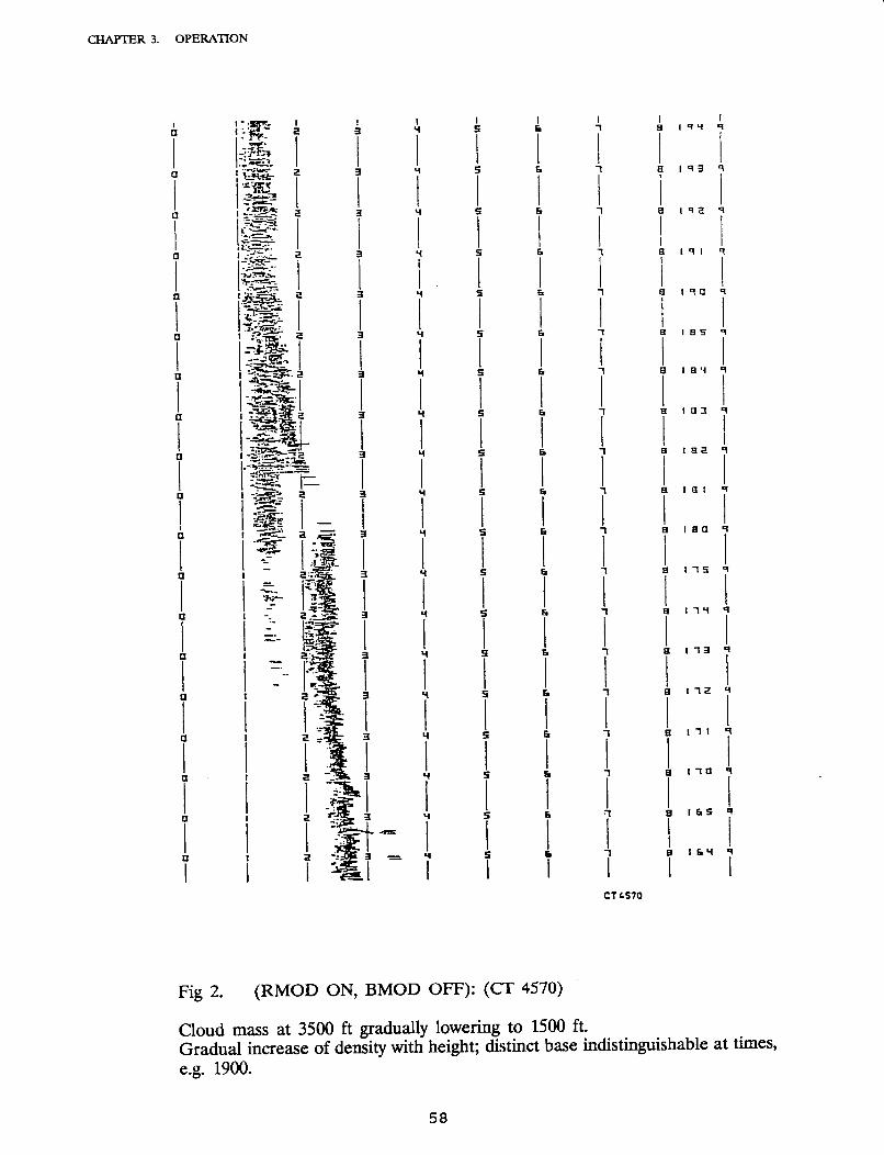
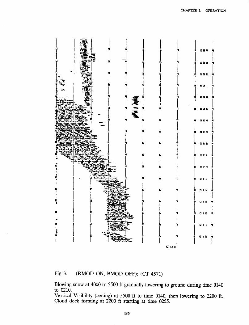
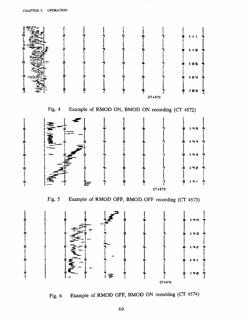
FIG 1 CT 4569FIG 2 CT 4570FIG 3 CT 4571FIG 4 CT 4572FIG 5 CT 4573FIG 6 CT 4574
CT 4413CT 4411CT 4412
U.CT 1104U.CT.CT 2101
CT 2295A.CT 3400A.CT 3401A.CT 3402A.CT 3403A.CT 3404A.CT 3405ACT 3406A.CT 4407
CT 4532CT 3501CT 3385CT 3386CT 3387CT 3388CT 3544
C.CT 2492CT 3536CT 3196
C.CT 2294CT 2277
REV DESCRIPTION PAGE
CCB.a
;A
i3BBBB
AA
8”ADACBCEB
CT 12K CeilometerCT 12K InstallationCT 12K Connection DiagramCT 12K Equipment Base, Bottom ViewRMOD On, BMOD OffRMOD On, BMOD OffRMOD On, BMOD OffRMOD On, BMOD OnRMOD Off, BMOD OffRMOD Off, BMOD OnActual Return SignalDiagram of Internal CyclesDiagram of Recorder OutputsCT 12K Wiring DiagramCT 12K Generation Breakdown ChartCT 12K Block DiagramCT 12K General LayoutCT 12K Internal Layout, Front ViewCT 12K Internal Layout, Rear ViewCT 12K Internal Layout, Right Hand ViewCT 12K Internal Layout, Left Hand ViewCT 12K Internal Layout, Top ViewCT 12K Equipment Base, Bottom ViewCT 12K Processor Board CTM 12 Jumpers & ConnectorsCTM 12 Main Functions and Primary Data/Control FlowCTM 12 Processor Board Principle Block DiagramCTM 12 Processor Board Circuit Diagram l/4 (CPU)CTM 12 Processor Board Circuit Diagram 2/4 (Monitor)CTM 12 Processor Board Circuit Diagram 3/4 (Seq.Cont)CTM 12 Processor Board Circuit Diagram 4/4 (Amp)CTM 12 Processor Board CPU Cycle TimingCTM 12 Processor Board Component LayoutCTM 12 Processor Board Pulse DiagramCTS 12 Unreg. Power Sup. Circuit DiagramCTS 12 Unreg. Power Sup. Components LayoutCTI 12 Output Interface Circuit Diagram
242526
z::585960606097
107112117119120121122123124125126127157158159160161162163164165166173174183
vii
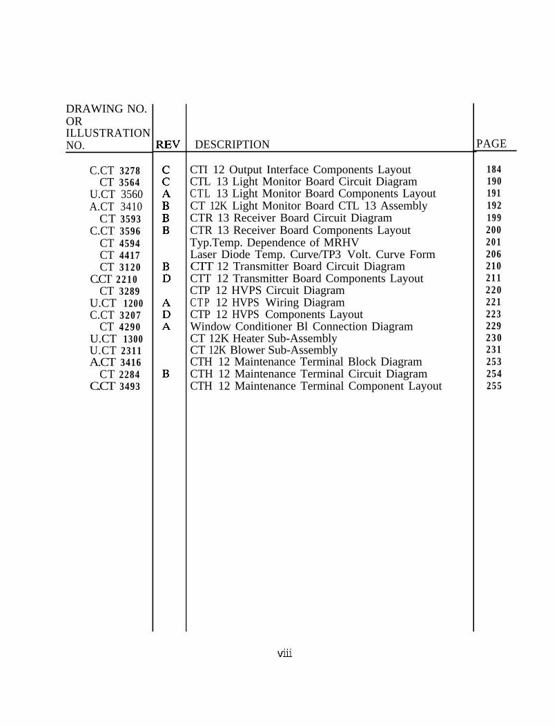
DRAWING NO.ORILLUSTRATIONNO.
C.CT 3278CT 3564
U.CT 3560A.CT 3410
CT 3593C.CT 3596
CT 4594CT 4417CT 3120
C.CT 2210CT 3289
U.CT 1200C.CT 3207
CT 4290U.CT 1300U.CT 2311A.CT 3416
CT 2284C.CT 3493
DESCRIPTION
CTI 12 Output Interface Components Layout 184CTL 13 Light Monitor Board Circuit Diagram 190CTL 13 Light Monitor Board Components Layout 191CT 12K Light Monitor Board CTL 13 Assembly 192CTR 13 Receiver Board Circuit Diagram 199CTR 13 Receiver Board Components Layout 200Typ.Temp. Dependence of MRHV 201Laser Diode Temp. Curve/TP3 Volt. Curve Form 206CTT 12 Transmitter Board Circuit Diagram 210CTT 12 Transmitter Board Components Layout 211CTP 12 HVPS Circuit Diagram 220C T P 12 HVPS Wiring Diagram 221CTP 12 HVPS Components Layout 223Window Conditioner Bl Connection Diagram 229CT 12K Heater Sub-Assembly 230CT 12K Blower Sub-Assembly 231CTH 12 Maintenance Terminal Block Diagram 253CTH 12 Maintenance Terminal Circuit Diagram 254CTH 12 Maintenance Terminal Component Layout 255
PAGE
. . .vll l
Archive
viii

LIST OF TABLES
NUMBER DESCRIPTION PAGE
CT 3415 Monitored Parameters 90CT 4577 Contents of Character ROM 242
ix
Archive
Archive
Archive

x
Archive
x
Archive
SECTION
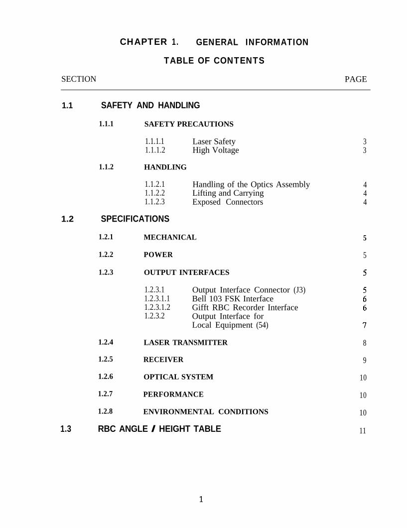
CHAPTER 1. GENERAL INFORMATION
TABLE OF CONTENTS
PAGE
1.1 SAFETY AND HANDLING
1.1.1 SAFETY PRECAUTIONS
1.1.1.1 Laser Safety 31.1.1.2 High Voltage 3
1.1.2 HANDLING
1.1.2.1 Handling of the Optics Assembly 41.1.2.2 Lifting and Carrying 41.1.2.3 Exposed Connectors 4
1.2 SPECIFICATIONS
1.2.1 MECHANICAL 5
1.2.2 POWER
1.2.3 OUTPUT INTERFACES
1.2.3.11.2.3.1.11.2.3.1.21.2.3.2
Output Interface Connector (J3)Bell 103 FSK InterfaceGifft RBC Recorder InterfaceOutput Interface forLocal Equipment (54)
1.2.4 LASER TRANSMITTER
1.2.5 RECEIVER
1.2.6 OPTICAL SYSTEM
1.2.7 PERFORMANCE 10
1.2.8 ENVIRONMENTAL CONDITIONS 10
1.3 RBC ANGLE / HEIGHT TABLE 11
5
8
9
10
Archive
1

2
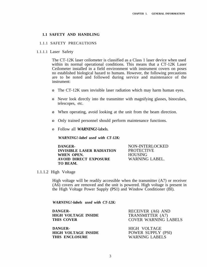
CHAPTER 1. GENERAL INFORMATION
1.1 SAFETY AND HANDLING
1.1.1 SAFETY PRECAUTIONS
1.1.1.1 Laser Safety
The CT-12K laser ceilometer is classified as a Class 1 laser device when usedwithin its normal operational conditions. This means that a CT-12K LaserCeilometer installed in a field environment with instrument covers on posesno established biological hazard to humans. However, the following precautionsare to be noted and followed during service and maintenance of theinstrument:
The CT-12K uses invisible laser radiation which may harm human eyes.
Never look directly into the transmitter with magnifying glasses, binoculars,telescopes, etc.
When operating, avoid looking at the unit from the beam direction.
Only trained personnel should perform maintenance functions.
Follow all WARNING!-labels.
WARNING!-label used with CT-12K:
DANGER-INVISIBLE LASER RADIATIONWHEN OPEN.AVOID DIRECT EXPOSURETO BEAM.
NON-INTERLOCKEDPROTECTIVEHOUSINGWARNING LABEL.
1.1.1.2 High Voltage
High voltage will be readily accessible when the transmitter (A7) or receiver(A6) covers are removed and the unit is powered. High voltage is present inthe High Voltage Power Supply (PS1) and Window Conditioner (Bl).
WARNING!-labels used with CT-12K:
DANGER- RECEIVER (A6) ANDHIGH VOLTAGE INSIDE TRANSMITTER (A7)THIS COVER COVER WARNING LABELS
DANGER- HIGH VOLTAGEHIGH VOLTAGE INSIDE POWER SUPPLY (PSl)THIS ENCLOSURE WARNING LABELS
3
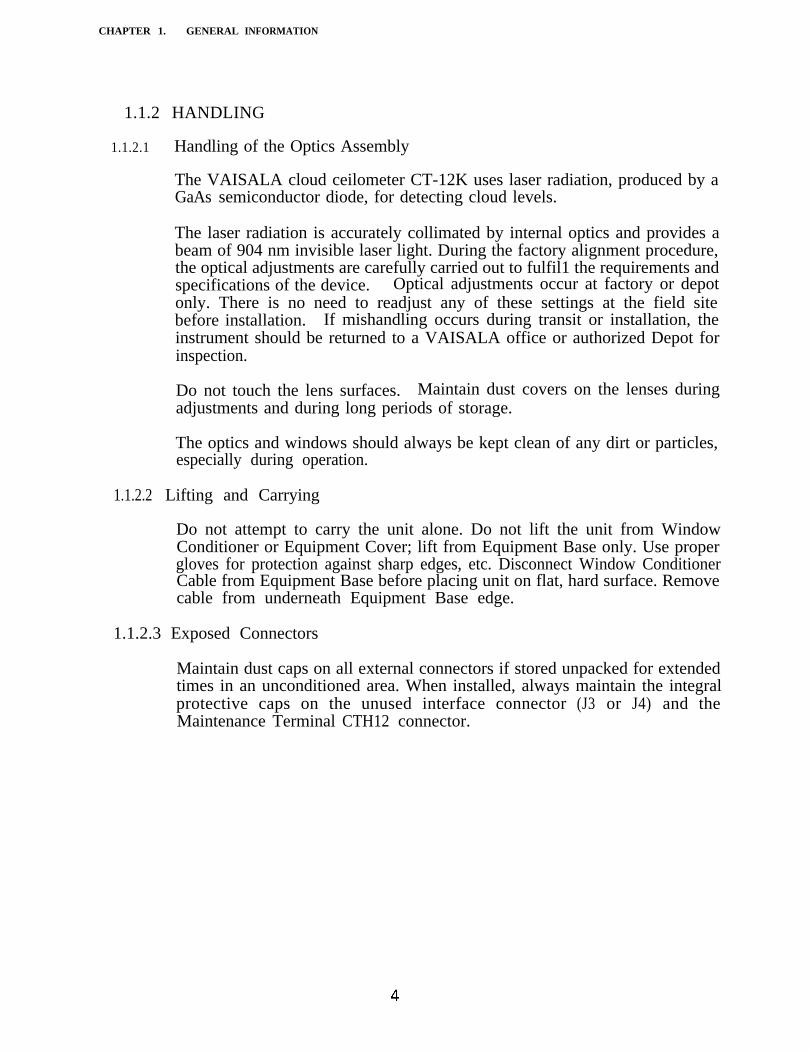
CHAPTER 1. GENERAL INFORMATION
1.1.2 HANDLING
1.1.2.1 Handling of the Optics Assembly
The VAISALA cloud ceilometer CT-12K uses laser radiation, produced by aGaAs semiconductor diode, for detecting cloud levels.
The laser radiation is accurately collimated by internal optics and provides abeam of 904 nm invisible laser light. During the factory alignment procedure,the optical adjustments are carefully carried out to fulfil1 the requirements andspecifications of the device. Optical adjustments occur at factory or depotonly. There is no need to readjust any of these settings at the field sitebefore installation. If mishandling occurs during transit or installation, theinstrument should be returned to a VAISALA office or authorized Depot forinspection.
Do not touch the lens surfaces. Maintain dust covers on the lenses duringadjustments and during long periods of storage.
The optics and windows should always be kept clean of any dirt or particles,especially during operation.
1.1.2.2 Lifting and Carrying
Do not attempt to carry the unit alone. Do not lift the unit from WindowConditioner or Equipment Cover; lift from Equipment Base only. Use propergloves for protection against sharp edges, etc. Disconnect Window ConditionerCable from Equipment Base before placing unit on flat, hard surface. Removecable from underneath Equipment Base edge.
1.1.2.3 Exposed Connectors
Maintain dust caps on all external connectors if stored unpacked for extendedtimes in an unconditioned area. When installed, always maintain the integralprotective caps on the unused interface connector (J3 or J4) and theMaintenance Terminal CTH12 connector.
Archive
4

CHAPTER 1. GENERAL INFORMATION
1.2 SPECIFICATIONS
1.2.1 MECHANICAL
Height: Total . . . . . 52.8 in. (1340 mm)Excluding Pedestal . . 29.1 in. ( 740 mm)Width . . . . . . . . . . . 22.8 in. ( 580 mm)Depth . . . . . . . . . . . 16.5 in. ( 420 mm)Weight: Total . . . 156 Lbs. (71 kg)
ExcludingPedestal 135 Lbs. (61 kg)
1.2.2 POWER
115 V ± 10% 45 Hz to 65 Hz 800 W (7 A) max.220 / 240 V (optional)Power connector (Jl): MIL-C-26482 type MS 3110E12-3P (male)
Mating connector type: MS 3116F12-3S or equivalent
1.2.3 OUTPUT INTERFACES
1.2.3.1 Output Interface Connector (J3)
MIL-C-26482 type MS 3112E12-8P (male)
Mating connector type: MS 3116F12-8S or equivalent
Circuit A-B: FSK InterfaceCircuit C-D: Recorder Trigger BreakCircuit E-F: Recorder Inscription (Cloud) SignalCircuit G: Equipment Ground
All signal circuits are non-polar, symmetrical; electrically floating to overvoltageprotection rating (300V-500V).
Overvoltage Protection in each circuit:
Primary. . . . ..Noble Gas Surge ArresterSecondary....Wirewound Resistors and Transient Zeners or Diodes
5
CHAPTER 1. GENERAL INFORMATION
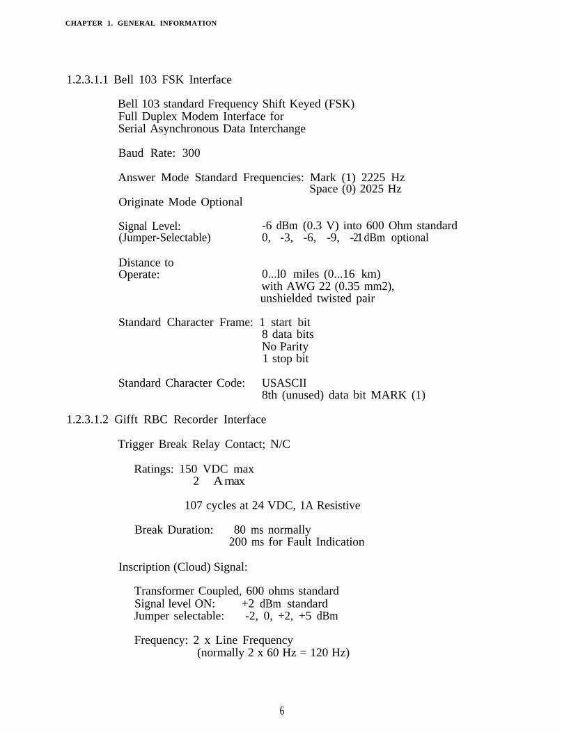
1.2.3.1.1 Bell 103 FSK Interface
Bell 103 standard Frequency Shift Keyed (FSK)Full Duplex Modem Interface forSerial Asynchronous Data Interchange
Baud Rate: 300
Answer Mode Standard Frequencies: Mark (1) 2225 HzSpace (0) 2025 Hz
Originate Mode Optional
Signal Level: -6 dBm (0.3 V) into 600 Ohm standard(Jumper-Selectable) 0, -3, -6, -9, - 12 dBm optional
Distance toOperate: 0...l0 miles (0...16 km)
with AWG 22 (0.35 mm2),unshielded twisted pair
Standard Character Frame: 1 start bit8 data bitsNo Parity1 stop bit
Standard Character Code: USASCII8th (unused) data bit MARK (1)
1.2.3.1.2 Gifft RBC Recorder Interface
Trigger Break Relay Contact; N/C
Ratings: 150 VDC max2 A max
107 cycles at 24 VDC, 1A Resistive
Break Duration: 80 ms normally200 ms for Fault Indication
Inscription (Cloud) Signal:
Transformer Coupled, 600 ohms standardSignal level ON: +2 dBm standardJumper selectable: -2, 0, +2, +5 dBm
Frequency: 2 x Line Frequency(normally 2 x 60 Hz = 120 Hz)
6
CHAPTER 1. GENERAL INFORMATION
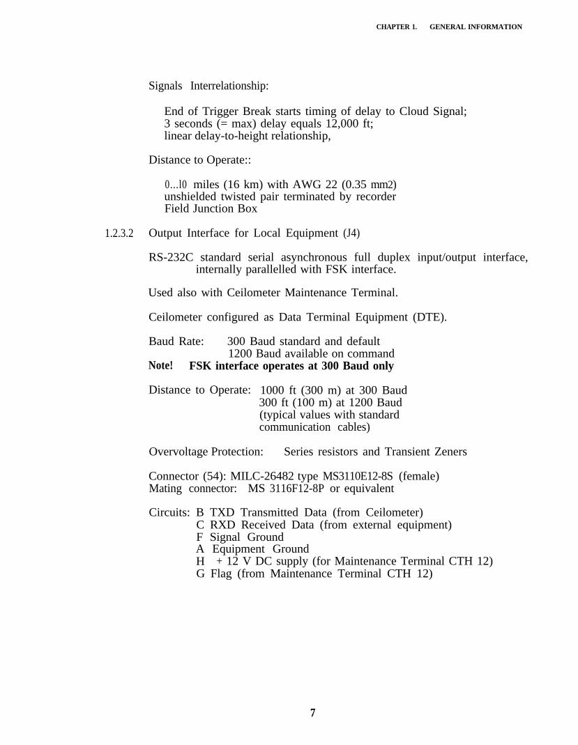
Signals Interrelationship:
End of Trigger Break starts timing of delay to Cloud Signal;3 seconds (= max) delay equals 12,000 ft;linear delay-to-height relationship,
Distance to Operate::
0...l0 miles (16 km) with AWG 22 (0.35 mm2)unshielded twisted pair terminated by recorderField Junction Box
1.2.3.2 Output Interface for Local Equipment (J4)
RS-232C standard serial asynchronous full duplex input/output interface,internally parallelled with FSK interface.
Used also with Ceilometer Maintenance Terminal.
Ceilometer configured as Data Terminal Equipment (DTE).
Baud Rate: 300 Baud standard and default1200 Baud available on command
Note! FSK interface operates at 300 Baud only
Distance to Operate: 1000 ft (300 m) at 300 Baud300 ft (100 m) at 1200 Baud(typical values with standardcommunication cables)
Overvoltage Protection: Series resistors and Transient Zeners
Connector (54): MILC-26482 type MS3110E12-8S (female)Mating connector: MS 3116F12-8P or equivalent
Circuits: B TXD Transmitted Data (from Ceilometer)C RXD Received Data (from external equipment)F Signal GroundA Equipment GroundH + 12 V DC supply (for Maintenance Terminal CTH 12)G Flag (from Maintenance Terminal CTH 12)
7
CHAPTER 1. GENERAL INFORMATION
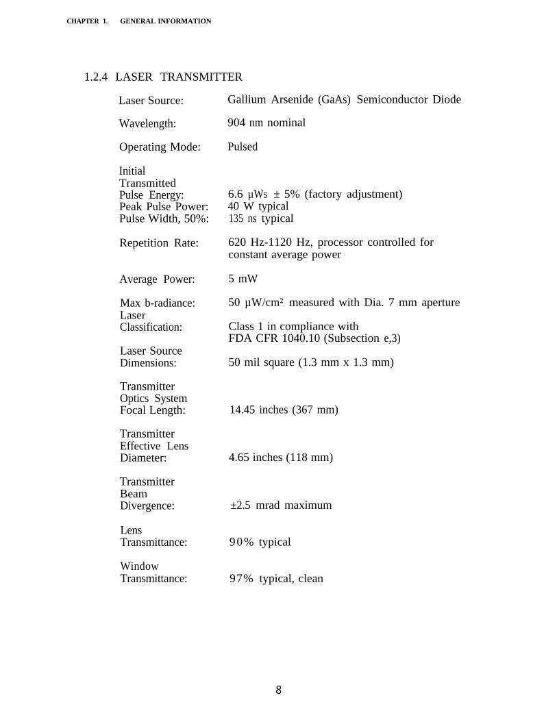
1.2.4 LASER TRANSMITTER
Laser Source:
Wavelength:
Operating Mode:
InitialTransmittedPulse Energy:Peak Pulse Power:Pulse Width, 50%:
Repetition Rate:
Average Power:
Max b-radiance:LaserClassification:
Laser SourceDimensions:
TransmitterOptics SystemFocal Length:
TransmitterEffective LensDiameter:
TransmitterBeamDivergence:
LensTransmittance:
WindowTransmittance:
Gallium Arsenide (GaAs) Semiconductor Diode
904 nm nominal
Pulsed
6.6 µWs ± 5% (factory adjustment)40 W typical135 ns typical
620 Hz-1120 Hz, processor controlled forconstant average power
5 mW
50 µW/cm² measured with Dia. 7 mm aperture
Class 1 in compliance withFDA CFR 1040.10 (Subsection e,3)
50 mil square (1.3 mm x 1.3 mm)
14.45 inches (367 mm)
4.65 inches (118 mm)
±2.5 mrad maximum
90% typical
97% typical, clean
Archive
8
CHAPTER 1. GENERAL INFORMATION
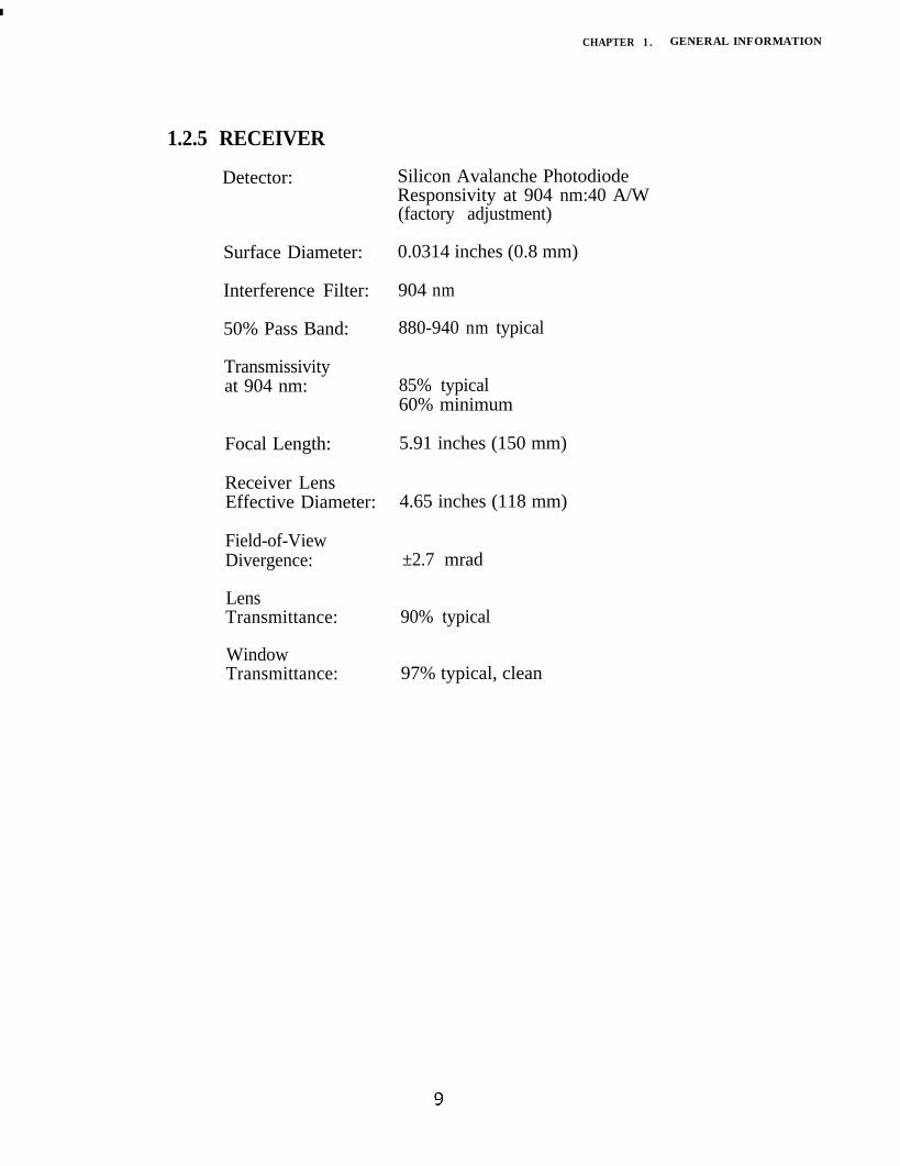
1.2.5 RECEIVER
Detector:
Surface Diameter:
Interference Filter:
50% Pass Band:
Transmissivityat 904 nm:
Focal Length:
Receiver LensEffective Diameter:
Field-of-ViewDivergence:
LensTransmittance:
WindowTransmittance:
Silicon Avalanche PhotodiodeResponsivity at 904 nm:40 A/W(factory adjustment)
0.0314 inches (0.8 mm)
904 nm
880-940 nm typical
85% typical60% minimum
5.91 inches (150 mm)
4.65 inches (118 mm)
±2.7 mrad
90% typical
97% typical, clean
Archive
9
CHAPTER 1. GENERAL INFORMATION
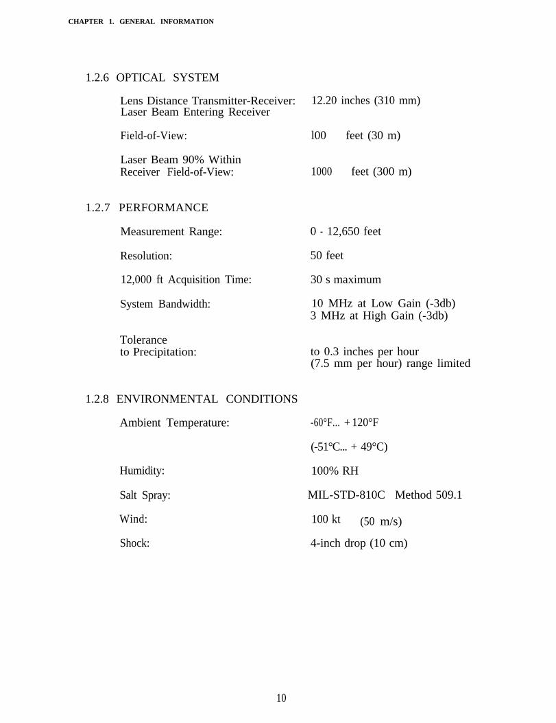
1.2.6 OPTICAL SYSTEM
Lens Distance Transmitter-Receiver: 12.20 inches (310 mm)Laser Beam Entering Receiver
Field-of-View:
Laser Beam 90% WithinReceiver Field-of-View:
l00 feet (30 m)
1000 feet (300 m)
1.2.7 PERFORMANCE
Measurement Range: 0 - 12,650 feet
Resolution: 50 feet
12,000 ft Acquisition Time: 30 s maximum
System Bandwidth: 10 MHz at Low Gain (-3db)3 MHz at High Gain (-3db)
Toleranceto Precipitation: to 0.3 inches per hour
(7.5 mm per hour) range limited
1.2.8 ENVIRONMENTAL CONDITIONS
Ambient Temperature: -60°F... + 120°F
(-51°C... + 49°C)
Humidity: 100% RH
Salt Spray:
Wind:
MIL-STD-810CMILSTD-810C Method 509.1
100 kt (50 m/s)
Shock: 4-inch drop (10 cm)
10
CHAPTER 1. GENERAL INFORMATION
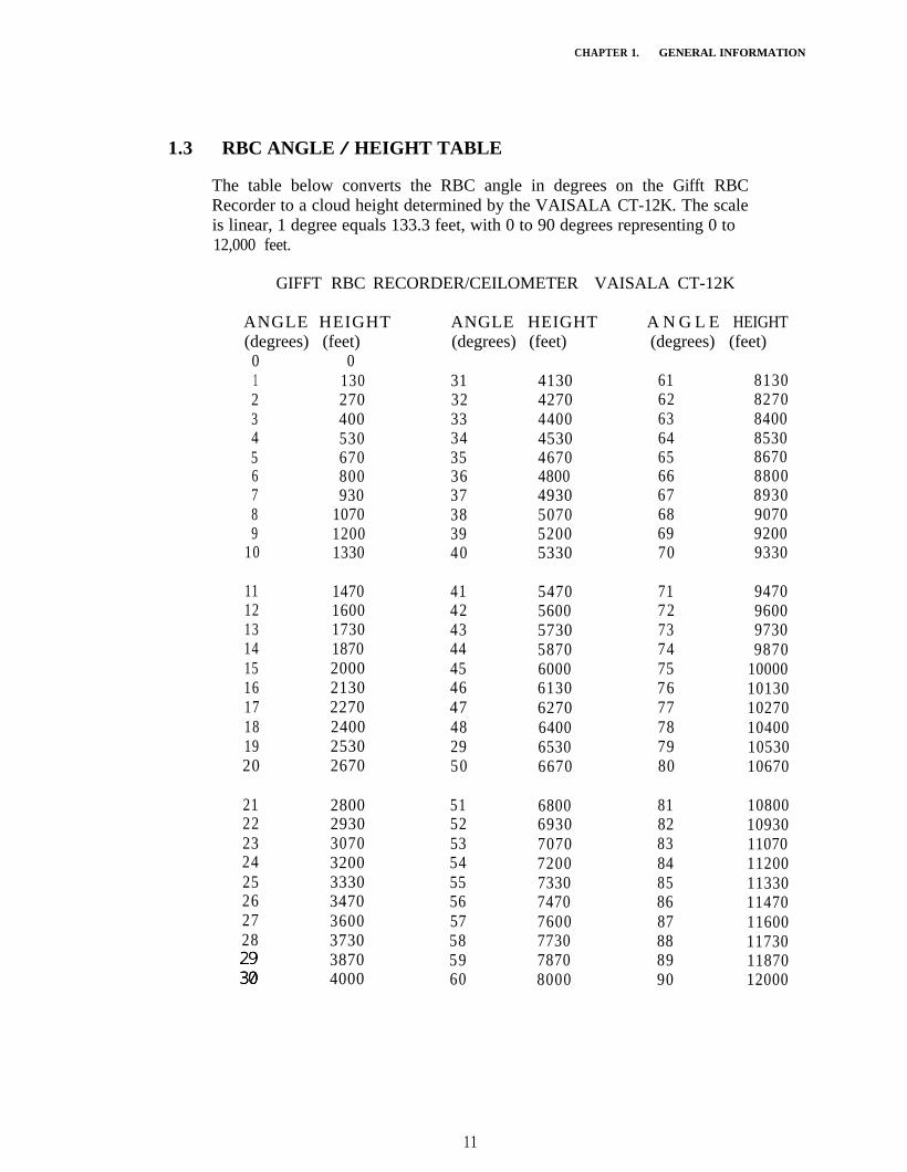
1.3 RBC ANGLE / HEIGHT TABLE
The table below converts the RBC angle in degrees on the Gifft RBCRecorder to a cloud height determined by the VAISALA CT-12K. The scaleis linear, 1 degree equals 133.3 feet, with 0 to 90 degrees representing 0 to12,000 feet.
GIFFT RBC RECORDER/CEILOMETER VAISALA CT-12K
ANGLE HEIGHT(degrees) (feet)0 01 1302 2703 4004 5305 6706 8007 9308 10709 1200
10 1330
ANGLE HEIGHT A N G L E HEIGHT(degrees) (feet) (degrees) (feet)
31 4130 61 813032 4270 62 827033 4400 63 840034 4530 64 853035 4670 65 867036 4800 66 880037 4930 67 893038 5070 68 907039 5200 69 920040 5330 70 9330
11 1470 41 5470 71 947012 1600 42 5600 72 960013 1730 43 5730 73 973014 1870 44 5870 74 987015 2000 45 6000 75 1000016 2130 46 6130 76 1013017 2270 47 6270 77 1027018 2400 48 6400 78 1040019 2530 29 6530 79 1053020 2670 50 6670 80 10670
2122232425262728
:;
2800 51 6800 81 108002930 52 6930 82 109303070 53 7070 83 110703200 54 7200 84 112003330 55 7330 85 113303470 56 7470 86 114703600 57 7600 87 116003730 58 7730 88 117303870 59 7870 89 118704000 60 8000 90 12000
11
Archive
29 30

12

13

14
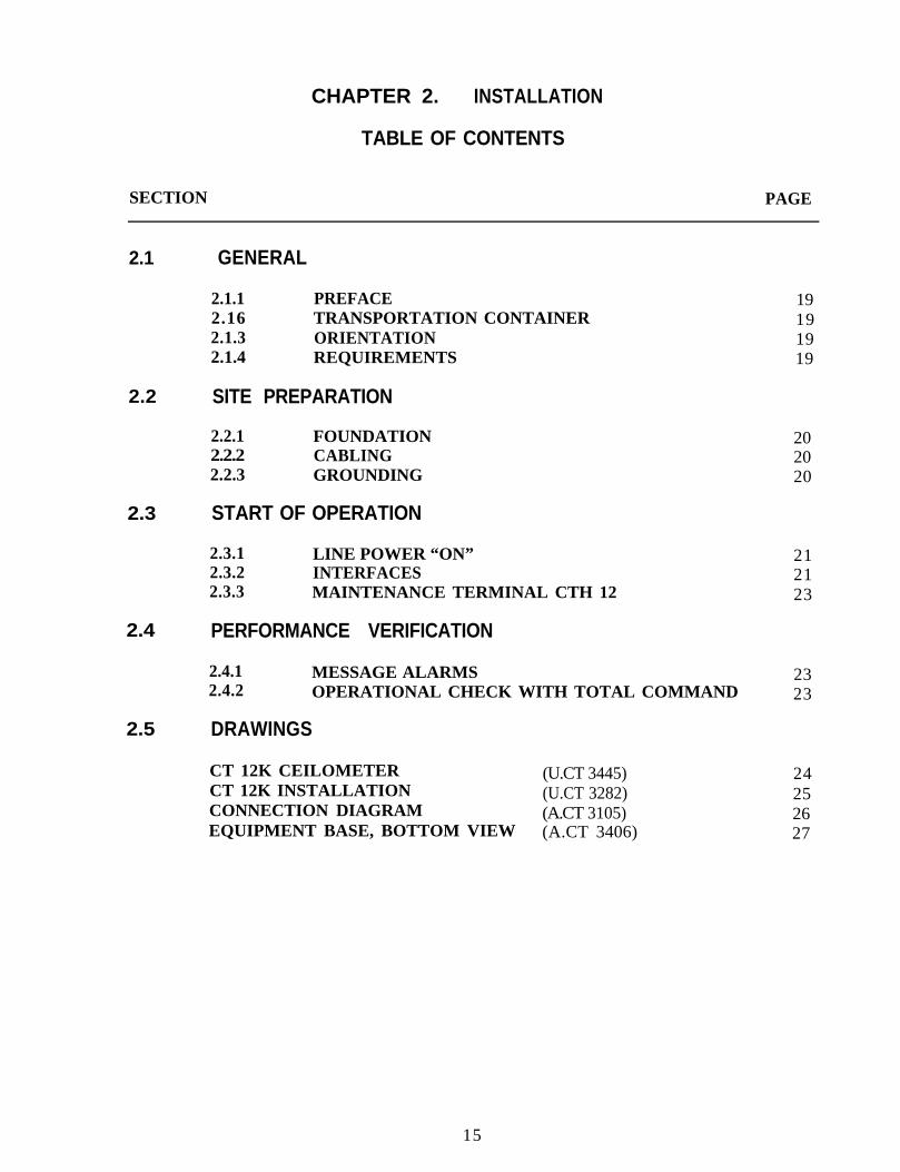
CHAPTER 2. INSTALLATION
TABLE OF CONTENTS
SECTION PAGE
2.1 GENERAL
2.2
2.1.1 PREFACE2.16 TRANSPORTATION CONTAINER2.1.3 ORIENTATION2.1.4 REQUIREMENTS
SITE PREPARATION
2.3
2.2.1 FOUNDATION2.2.2 CABLING2.2.3 GROUNDING
START OF OPERATION
2.4
2.3.1 LINE POWER “ON”2.3.2 INTERFACES2.3.3 MAINTENANCE TERMINAL CTH 12
PERFORMANCE VERIFICATION
2.5
2.4.1 MESSAGE ALARMS2.4.2 OPERATIONAL CHECK WITH TOTAL COMMAND
DRAWINGS
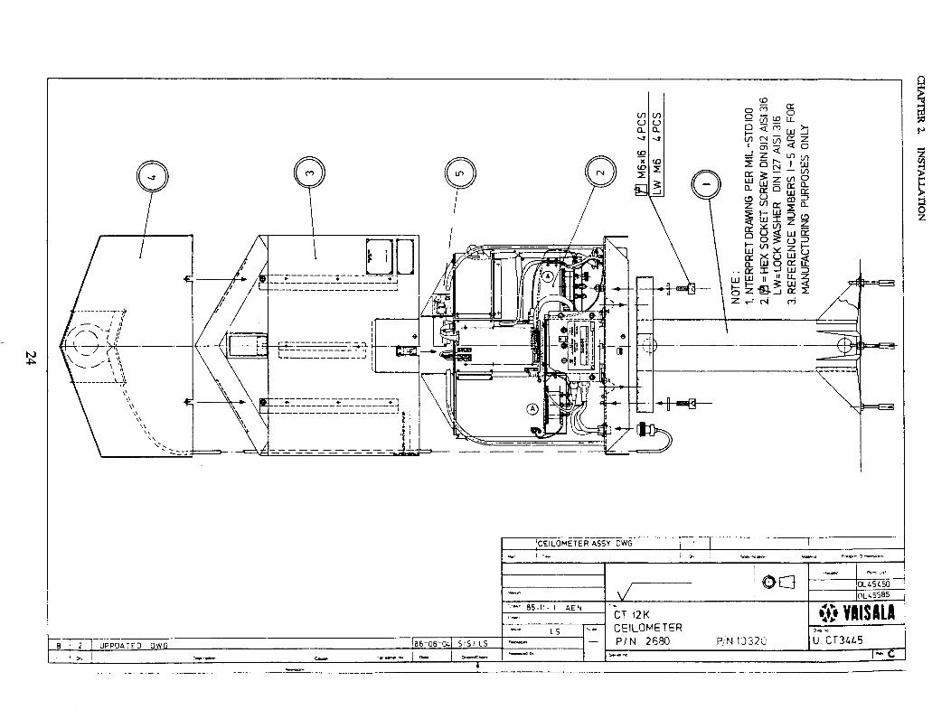
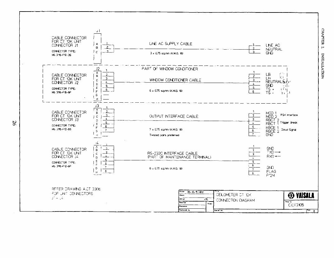
CT 12K CEILOMETERCT 12K INSTALLATION
(U.CT 3445)
CONNECTION DIAGRAM(U.CT 3282)
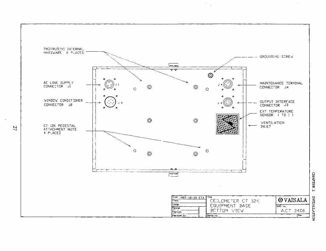
EQUIPMENT BASE, BOTTOM VIEW(A.CT 3105)(A.CT 3406)
19191919
202020
212123
2323
24252627
15

16
Archive
16
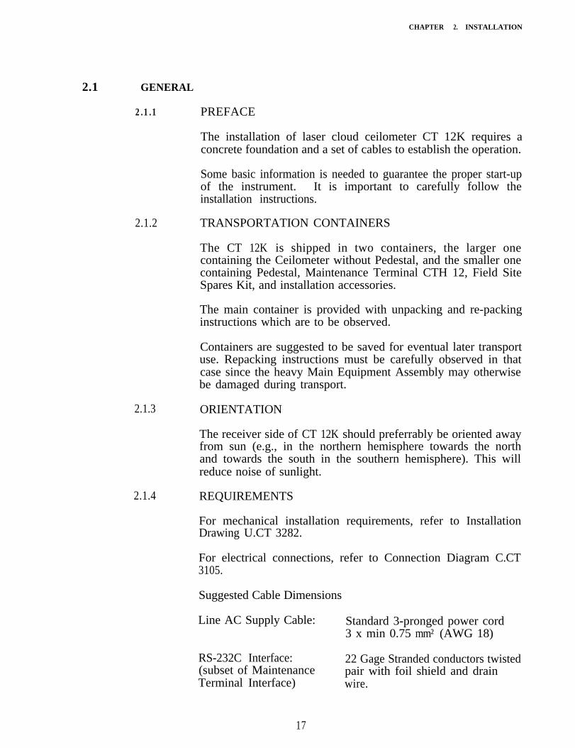
CHAPTER 2. INSTALLATION
2.1 GENERAL
2.1.1 PREFACE
The installation of laser cloud ceilometer CT 12K requires aconcrete foundation and a set of cables to establish the operation.
Some basic information is needed to guarantee the proper start-upof the instrument. It is important to carefully follow theinstallation instructions.
2.1.2 TRANSPORTATION CONTAINERS
The CT 12K is shipped in two containers, the larger onecontaining the Ceilometer without Pedestal, and the smaller onecontaining Pedestal, Maintenance Terminal CTH 12, Field SiteSpares Kit, and installation accessories.
The main container is provided with unpacking and re-packinginstructions which are to be observed.
Containers are suggested to be saved for eventual later transportuse. Repacking instructions must be carefully observed in thatcase since the heavy Main Equipment Assembly may otherwisebe damaged during transport.
2.1.3 ORIENTATION
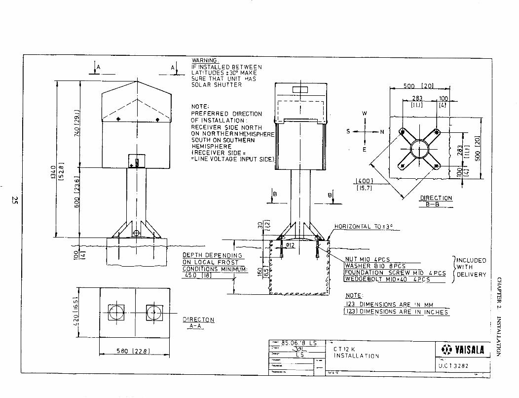
The receiver side of CT 12K should preferrably be oriented awayfrom sun (e.g., in the northern hemisphere towards the northand towards the south in the southern hemisphere). This willreduce noise of sunlight.
2.1.4 REQUIREMENTS
For mechanical installation requirements, refer to InstallationDrawing U.CT 3282.
For electrical connections, refer to Connection Diagram C.CT3105.
Suggested Cable Dimensions
Line AC Supply Cable: Standard 3-pronged power cord3 x min 0.75 mm² (AWG 18)
RS-232C Interface:(subset of MaintenanceTerminal Interface)
22 Gage Stranded conductors twistedpair with foil shield and drainwire.
17
CHAPTER 2. INSTALLATION
Output Interface Cable(Twisted Pairs Preferred)
22 Gage stranded conductors 3twisted pairs with foil shieldand drain wire. Minimum workingvoltage 200 volts.
Window Conditioner Cable: 6 x min 0.75 mm² (AWG 18)(Part of Window Conditioner,supplied)
Maintenance TerminalCable:(Part of MaintenanceTerminal, supplied)
8 x 0.75 mm² (AWG 18)
2.2 SITE PREPARATION
2.2.1 FOUNDATION
The suggested minimum dimensions for the foundation are foundin Installation Drawing U.CT 3282.
Mounting hardware is included with the Pedestal.
If a new foundation is laid, the Wedge Bolts and FoundationScrews (4 each), are suggested to be cast into the concrete sothat 1 to 2 inches (25 to 50 mm) of the threads stand above thesurface.
If an existing foundation is used, four holes of Diameter 0.5inches x 6.5 inches (12 mm x 165 mm) are drilled into theconcrete. The Wedge Bolt and Foundation Screw combinationsare placed in the holes, with Wedge Bolts down; the protrudingthreads are alternately hammered and tightened a few times sothat the Wedge Bolts attach to the hole walls.
18
CHAPTER 2. INSTALLATION
2.2.2 CABLING
All the cable connectors are located under the equipment baseand are referred to as Jl, J2, J3, and J4.
The location of the connectors are found in Bottom ViewDrawing ACT 3406.
The connector signals and connector types are found in theConnection Diagram C.CT 3105.
Mating connectors for Jl (Power) and J3 (Output Interface) aresupplied with the Ceilometer.
2.2.3 GROUNDING
The power supply connector Jl provides a standard protectiveground for the instrument chassis.Connection of an external earthing shall be made to the groundterminal of the equipment base (reference: A.CT 3406 forlocation).CONNECTION TO A SOLID EARTH GROUND AT THEINSTALLATION SITE IS MANDATORY FOR ADEQUATELIGHTNING AND TRANSIENT PROTECTION.
19
CHAPTER 2. INSTALLATION
2.3 START OF OPERATION
2.3.1 LINE POWER “ON”
Before plugging in any connectors, check the field cables referredto in the Connection Diagram C.CT 3105.
Remove the unit covers of CT 12K and make a visual check ofthe internal connectors, subassemblies, etc.
Turn the main circuit breaker CBl to “OFF” position.
Plug in the line supply cable to connector Jl after checking thevoltage and signals of the power supply cable connector.
The line voltage indicator DSl in PSl should be lit indicatingthe line voltage at the main circuit breaker CBl.
When turning the main circuit breaker CBl to the “ON” position,the following shall happen with the monitoring LEDs D4 and D5on the processor board, Al:
D4 (red) “ON” for approximately 5 seconds (internalreset performed).
D5 (green) After D4 has turned “OFF”, this willstart blinking at a rate of once per second (softwareoperates normally)
If LEDs D4 and D5 operate differently, the unitneeds service or maintenance. Refer to Chapter 6,‘Troubleshooting”.
20
CHAPTER 2. INSTALLATION
2.3.2 INTERFACES
The CT 12K provides three (3) different interfaces for remotedevices:
0 RS-232C Maintenance Terminal Interface0 Bell 103 Modem Interface0 Gifft RBC Recorder Interface
Depending on the distance between the Ceilometer and theobserver site, the data communication can be arranged either withthe RS-232C level direct connection (up to 1000 feet) or with theBell 103 modem connection (for distances exceeding 1000 feet).
The RS-232C (Maintenance Terminal) connection signals areavailable at CT 12K equipment base connector J4.
The Gifft RBC Recorder interface consists of two (2) signal pairs:
0 Recorder sweep synchronization (trigger break)0 Cloud Data signal
The modem signals and Gifft RBC Recorder signals are availablethrough connector J3. Reference Connection Diagram C.CT3105.
The CTI 12 Interface Board (Reference A3) provides five LEDsfor monitoring the communication:
0 D10
0 Dll
0 Dl2
0 D13
0 D14
(yellow) TXD (Transmitted Data) Indicatesa presence of data being transmitted fromthe processor board Al, either via themodem circuitry or via the RS-232C
(yellow) RXD (Received Data) Datareceived via the modem line
(green) CD (Carrier Detect) Indicates thepresence of a carrier in the receive channelof the modem communication
(yellow) RBCT (RBC-recorder TriggerBreak) Gifft RBC Recorder pen sweep startand synchronization signal
(yellow) RBCE (RBC-recorder EnableCloud Signal) Gifft RBC Recorder clouddata signal
Archive
21
CHAPTER 2. INSTALLATION
2.3.3
These LEDs provide an easy means to check and monitor theoperation of the communication.
After “POWER UP”, the following sequence is performedautomatically ‘by the CT 12K software:
0 Data transmission starts with the data memory andmodem test messages, and "TXD" will blinkaccording to the character stream.
0 The modem circuitry and communication lines, ifused, are tested and the communication isestablished. “CD” will be turned on for 2 - 3seconds while the testing is performed, then remains“OFF” except when an active counter-modem withcarrier “ON” is connected to J3.
0 Modem test, program memory tests and internalstatus messages are transmitted and "TXD" willindicate the presence of transmission.
In the normal operation mode (Automatic mode) the cloud datacollection and the calculations take maximum of 30 seconds toprovide the first message table. When the message is sent, "TXD"will indicate the character stream of transmission for serialcommunications (RS-232C or Modem).
The Gifft RBC Recorder output LEDs D13, and D14 shall startoperating according to the interface specifications in 12 seconds.
However, the automatic measurements of the Ceilometer may beterminated for maintenance purposes by using the AUTO OFFcommand. Refer to Chapter 3, “Operation.” In the maintenancemode, most of the functions can be individually activated and,therefore, easily tested.
After monitoring the operation with the LEDs on Al and A3,the cables can be connected to the connectors J3 and J4.
The operation should continue as described earlier. If not, thenthe cables, operators’ terminals, etc., should be checked andpossible mistakes corrected.
MAINTENANCE TERMINAL CTH 12
While operating at the installation site, the Maintenance TerminalCTH 12 provides an easy way to monitor and control theoperation of the Ceilometer. Refer to Chapter 3.
The Maintenance Terminal is connected to connector J4 of theequipment base.
22
CHAPTER 2. INSTALLATION
2.4 PERFORMANCE VERIFICATION
2.4.1 MESSAGE ALARMS
Check that the Start-Up Message (Reference Paragraph 3.4.3)does not contain any messages of alarm, error or suspicion, andthat none of the numerical values output in the message has anasterisk ("*") immediately after it.
After Start-Up, observe operation for a suitable time. Check thatno alarms are generated.
If cause for suspicion exists, turn to Chapter 6 .
2.4.2 OPERATIONAL CHECK WITH TOTAL COMMAND
The CT 12K Ceilometers are factory adjusted and aligned foroptimum performance.
After installation, the operation can be checked with a constantand solid cloud base within the height range of 1000 - 5000 ftwith no fog, haze or precipitation. The TOTAL command of theCT 12K software is used for this purpose.
To use the TOTAL command, proceed as follows:
0 Open the communication line giving a “CR” symbol(CR = Carriage Return from the Operator’sTerminal)
0 Give “TOTAL” command and “CR”
The CT 12K software responds to this by giving the parametervalue (TOTAL SIGNAL LIMIT) and the measured total value(CURRENT SIGNAL SUM).
The “SUM” values reported in above conditions should be inrange 20...40. If out of limits, then turn to Chapter 6.
For exact command syntaxes and additional information, seeSection 3.4.
23

28

29

30
SECTION
CHAPTER 3. OPERATION
TABLE OF CONTENTS
PAGE
3.1 GENERAL
3.1.1 INTRODUCTION: NORMAL, OPERATION3.1.2 SWITCHES3.1.3 INDICATORS
3.1.4 USE OF SERIAL DIGITAL INTERFACE
3.1.4.1 General 373.1.4.2 Frame, Code and Speed 373.1.4.3 Notations and Abbreviations 383.1.4.4 Line Closed - Line Open 393.1.4.5 Command Format and Editing Rules 403.1.4.6 Advanced Information 41
3.1.5 AUTOMATIC MODE - MAINTENANCE MODE
3.1.6 FAST HEATER OFF
3.2 STANDARD OUTPUTS
36.1 DIGITAL MESSAGE NO. 2
3.2.1.1 General 443.2.1.2 Format 443.2.1.3 Status Line 1 453.2.1.4 Status Line 2 463.2.1.5 Data Line Format 473.2.1.6 Message Example 49
3.2.2 DIGITAL MESSAGE NO. 3
3.2.2.1 General3.2.2.2 Format3.2.2.3 Status Line 13.2.2.4 Backscatter Data Line3.2.2.5 Message Example
353536
41
43
515151
31
Archive
50 50
3.23 GIFFT RBC RECORDER OUTPUT
3.2.3.13.2.3.23.2.3.3
3.2.3.4
IntroductionSignalsRecording Modes and Set-UpCommandsExamples and Interpretation
3.3 PARAMATERS AND OPERATION MODES
3.3.1 STANDARD PARAMETER SETTINGS 613.3.2 DESCRIPTION OF PARAMETERS 62
3.4 PERFORMANCE MONITORING AND ALARMS
3.4.1 GENERAL3.4.2 STATUS MESSAGE3.4.3 START-UP3.4.4 ALARM LIMITS
3.4.5 COMMANDS FOR DETAILED CHECKING
3.4.5.13.4.5.23.4.5.33.4.5.43.4.5.53.4.5.63.4.5.73.4.5.83.4.5.93.4.5.103.4.5.113.4.5.123.4.5.133.4.5.143.4.5.153.4.5.163.4.5.173.4.5.183.4.5.19
LASES E QNOISFREQGAINHEATBLOWSHUTRECTTIMEDATERESECALHELPMEASTABGRAPMES
5252
5355
67
69
70717172727374747475757676777879798081
32
Archive
67 68
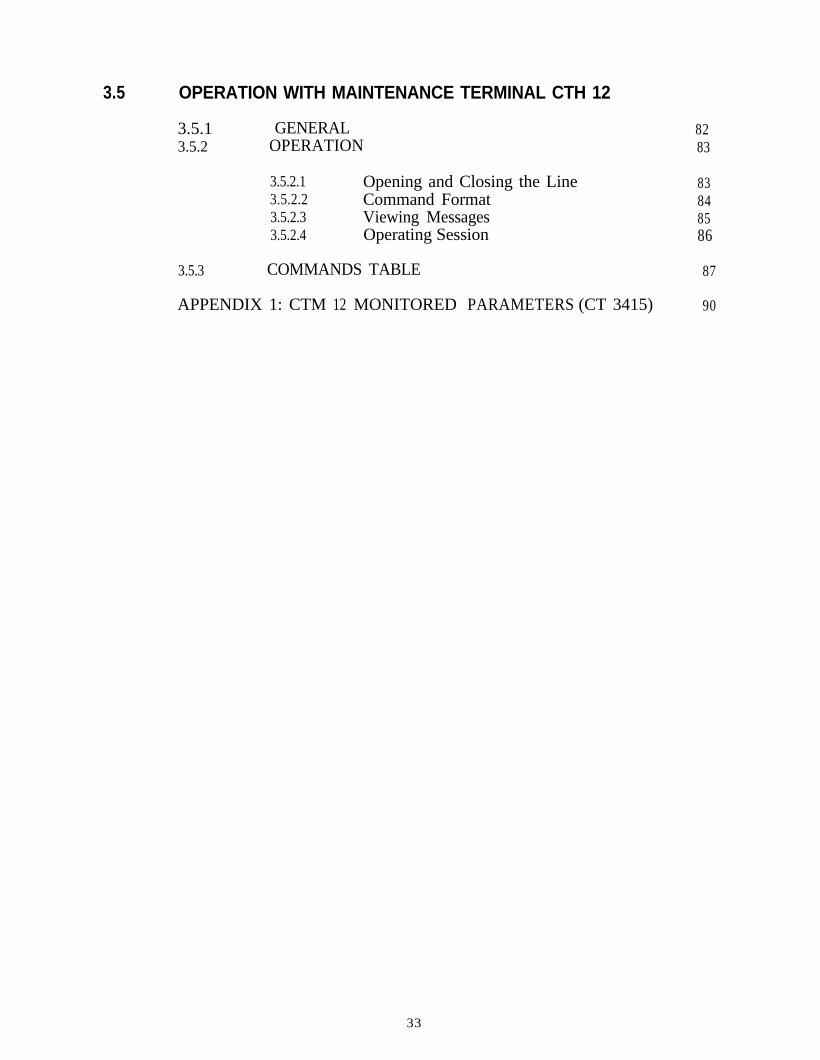
3.5 OPERATION WITH MAINTENANCE TERMINAL CTH 12
3.5.1 GENERAL 823.5.2 OPERATION 83
3.5.2.1 Opening and Closing the Line 833.5.2.2 Command Format 843.5.2.3 Viewing Messages 853.5.2.4 Operating Session 86
3.5.3 COMMANDS TABLE
APPENDIX 1: CTM 12 MONITORED PARAMETERS (CT 3415)
87
90
33

34
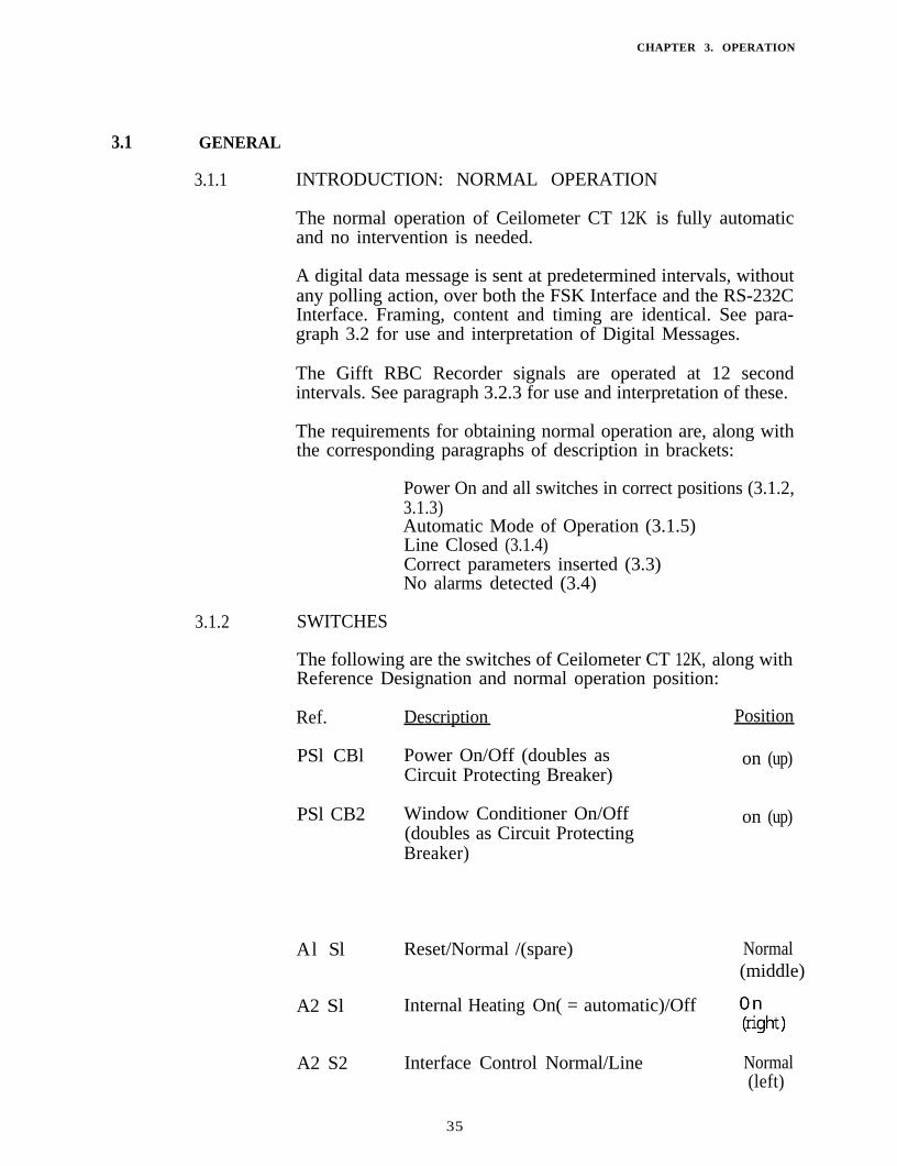
CHAPTER 3. OPERATION
3.1 GENERAL
3.1.1 INTRODUCTION: NORMAL OPERATION
The normal operation of Ceilometer CT 12K is fully automaticand no intervention is needed.
A digital data message is sent at predetermined intervals, withoutany polling action, over both the FSK Interface and the RS-232CInterface. Framing, content and timing are identical. See para-graph 3.2 for use and interpretation of Digital Messages.
The Gifft RBC Recorder signals are operated at 12 secondintervals. See paragraph 3.2.3 for use and interpretation of these.
The requirements for obtaining normal operation are, along withthe corresponding paragraphs of description in brackets:
Power On and all switches in correct positions (3.1.2,3.1.3)Automatic Mode of Operation (3.1.5)Line Closed (3.1.4)Correct parameters inserted (3.3)No alarms detected (3.4)
3.1.2 SWITCHES
The following are the switches of Ceilometer CT 12K, along withReference Designation and normal operation position:
Ref.
PSl CBl
Description
Power On/Off (doubles asCircuit Protecting Breaker)
PSl CB2 Window Conditioner On/Off(doubles as Circuit ProtectingBreaker)
Al Sl Reset/Normal /(spare)
A2 Sl
A2 S2
Internal Heating On( = automatic)/Off
Interface Control Normal/Line
Position
on (up)
on (up)
Normal(middle)
Normal(left)
35
Archive
On (right)
CHAPTER 3. OPERATION
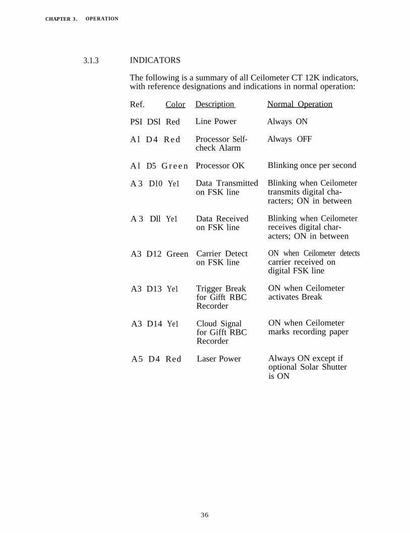
3.1.3 INDICATORS
The following is a summary of all Ceilometer CT 12K indicators,with reference designations and indications in normal operation:
Ref. Color
PSI DSl Red
A l D 4 R e d
A l D5 G r e e n
A 3 Dl0 Ye1
A 3 Dll Ye1
A3 D12 Green
A3 D13 Ye1
A3 D14 Ye1
A5 D4 Red
Description
Line Power
Processor Self-check Alarm
Processor OK
Data Transmittedon FSK line
Data Receivedon FSK line
Carrier Detecton FSK line
Trigger Breakfor Gifft RBCRecorder
Cloud Signalfor Gifft RBCRecorder
Laser Power
Normal Operation
Always ON
Always OFF
Blinking once per second
Blinking when Ceilometertransmits digital cha-racters; ON in between
Blinking when Ceilometerreceives digital char-acters; ON in between
ON when Ceilometer detectscarrier received ondigital FSK line
ON when Ceilometeractivates Break
ON when Ceilometermarks recording paper
Always ON except ifoptional Solar Shutteris ON
36
CHAPTER 3. OPERATION
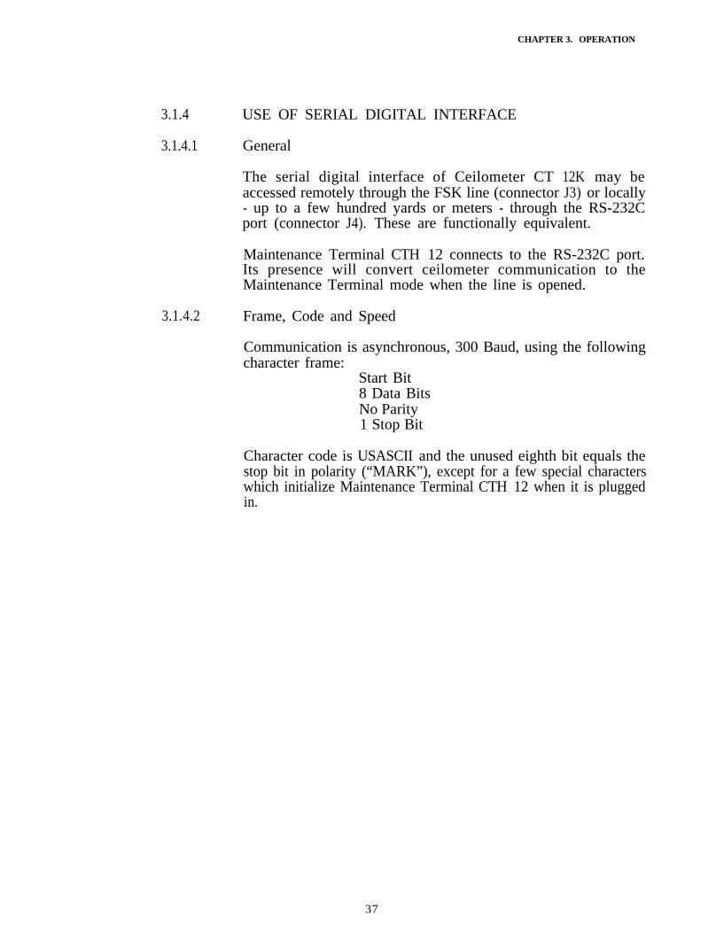
3.1.4 USE OF SERIAL DIGITAL INTERFACE
3.1.4.1 General
The serial digital interface of Ceilometer CT 12K may beaccessed remotely through the FSK line (connector J3) or locally- up to a few hundred yards or meters - through the RS-232Cport (connector J4). These are functionally equivalent.
Maintenance Terminal CTH 12 connects to the RS-232C port.Its presence will convert ceilometer communication to theMaintenance Terminal mode when the line is opened.
3.1.4.2 Frame, Code and Speed
Communication is asynchronous, 300 Baud, using the followingcharacter frame:
Start Bit8 Data BitsNo Parity1 Stop Bit
Character code is USASCII and the unused eighth bit equals thestop bit in polarity (“MARK”), except for a few special characterswhich initialize Maintenance Terminal CTH 12 when it is pluggedin.
37
CHAPTER 3. OPERATION
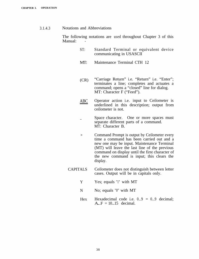
3.1.4.3 Notations and Abbreviations
The following notations are used throughout Chapter 3 of thisManual: -
ST: Standard Terminal or equivalent devicecommunicating in USASCII
MT: Maintenance Terminal CTH 12
(CR)
ABC
-
>
CAPITALS
Y
N
Hex
“Carriage Return” i.e. “Return” i.e. “Enter”;terminates a line; completes and actuates acommand; opens a “closed” line for dialog.MT: Character F (“Feed”).
Operator action i.e. input to Ceilometer isunderlined in this description; output fromceilometer is not.
Space character. One or more spaces mustseparate different parts of a command.MT: Character B.
Command Prompt is output by Ceilometer everytime a command has been carried out and anew one may be input. Maintenance Terminal(MT) will leave the last line of the previouscommand on display until the first character ofthe new command is input; this clears thedisplay.
Ceilometer does not distinguish between lettercases. Output will be in capitals only.
Yes; equals "1" with MT
No; equals "0" with MT
Hexadecimal code i.e. 0...9 = 0...9 decimal;A...F = 10...15 decimal.
38
Archive
CHAPTER 3. OPERATION
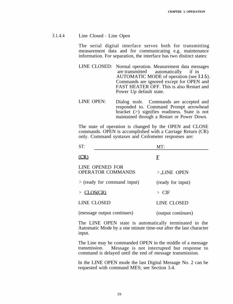
3.1.4.4 Line Closed - Line Open
The serial digital interface serves both for transmittingmeasurement data and for communicating e.g. maintenanceinformation. For separation, the interface has two distinct states:
LINE CLOSED: Normal operation. Measurement data messagesare transmitted automatically if in ’
AUTOMATIC MODE of operation (see 331.5)..Commands are ignored except for OPEN andFAST HEATER OFF. This is also Restart andPower Up default state.
LINE OPEN: Dialog mode. Commands are accepted andresponded to. Command Prompt arrowheadbracket (>) signifies readiness. State is notmaintained through a Restart or Power Down.
The state of operation is changed by the OPEN and CLOSEcommands. OPEN is accomplished with a Carriage Return (CR)only. Command syntaxes and Ceilometer responses are:
ST: MT:
LINE OPENED FOROPERATOR COMMANDS > LINE OPEN-
> (ready for command input) (ready for input)
> CLOS(CR) > ClF
LINE CLOSED LINE CLOSED
(message output continues) (output continues)
The LINE OPEN state is automatically terminated in theAutomatic Mode by a one minute time-out after the last characterinput.
The Line may be commanded OPEN in the middle of a messagetransmission. Message is not interrupted but response tocommand is delayed until the end of message transmission.
In the LINE OPEN mode the last Digital Message No. 2 can berequested with command MES; see Section 3.4.
39
Archive
Archive
3.1.5).
CHAPTER 3. OPERATION
3.1.4.5 Command Format and Editing Rules
The command consists of a command identifier (ID) and none,one, two, three or four groups of parameters (PARn). It isterminated by a Carriage Return (CR) which also actuates itsexecution. One or more spaces must separate identifier andparameters:
ID_PARl_PAR2(CR)
With input commands, new data values or states of operation aredefined by the parameter (one only). If the parameter is omitted,the current value or state will he output; with certain output com-mands, a default set of parameters will be used.
With standard ASCII communication (ST:) the identifier part con-sists of 2 to 4 letters. Additional letters will be ignored. Thepararneters are numbers or letter combinations. TheDEL(RUBOUT) key can be used for editing the command.
With Maintenance Terminal Communication (MT:) the identifierpart consists of letter C and a number code; these need not beseparated by space. The parameters are numbers, ON and YESis “1”; OFF and NO is "0" No DEL(RUBOUT) equivalent isavailable.
Numeric parameters may be input as they are written i.e. zeroesand decimal point are used as in writing.
All input characters are echoed.
40
CHAPTER 3. OPERATION
3.1.4.6 Advanced Information
Internally, Ceilometer CT 12K is equipped with one serial digitalinterface. This is used both for FSK and RS-232C electrical inter-face ports. Outputs are identical; inputs are ORed. Input devicesmay be simultaneously connected to RS-232C and FSK ports butmay not input characters simultaneously.
No handshake signals are used.
The RS-232C port (J4) doubles as a port for MaintenanceTerminal CTH 12. The presence of this special 16-key,16-character terminal is sensed by an input signal (‘FLAG”),whereupon an opening of the line will convert data interchangeto be in the Maintenance Terminal mode.
Output from Ceilometer may be stopped by issuing an XOFF( =Control- S = 13 hexadecimal). Output will commence uponreception of any character except XOFF. The BEL character isoutput in addition to that shown in this chapter:
when Line is Opened or Closedwhen a Syntax Error is encountered
All input parameters and operation modes are stored innon-volatile memory (EEPROM) except when specificallymentioned.
3.1.5 AUTOMATIC MODE - MAINTENANCE MODE
The Automatic Mode is the normal mode of operation; theMaintenance Mode is available for e.g. maintenance checking etc.The following is a summary of their operations:
AUTOMATIC Normal mode of operation. A measurementMODE cycle is (completed every 12 seconds. Outputs
according to 3.2 are active. The Digitalmessage is withheld if the line is “opened” foroperator dialog. Internal monitoring and controlsare updated every 15 seconds.
41
CHAPTER 3. OPERATION
MAINTENANCE Used temporarily for checking operation etc.MODE Measurement cycle is halted but may be
operated by command. Measurement calcu-lations are not performed. Internal settings andcontrols may be operated by commands.
No automatic time-out for closing an opencommunication line is applied.
The Maintenance Mode doubles as aSTANDBY MODE for minimizing wearout oflaser and moving parts. The WindowConditioner is operated automatically only thefirst 5 minutes every hour of the internal clock.
The following are the commands for setting the mode ofoperation, along with Ceilometer response. Omitting theparameter part (OFF/ ON or 0/l) results in response accordingto the prevailing mode:
ST: MT:
> AUTO OFF(CR) > CllB0F
WAIT FOR SEQUENCE STOP WAIT SEQ. STOP_
MAINTENANCE MODE >MAINT. MODE
> (next input) (next input)
> AUTO ON(CR) > CllBlF
AUTOMATIC MODE > AUTOMATIC MODE
> (next input) (next input)
The current 12 second measurement sequence is completed beforeswitching to Maintenance Mode.
The Mode selection will remain in effect over a Restart orPowerdown.
42
CHAPTER 3. OPERATION
3.1.6 FAST HEATER OFF
The 600W Window Conditioner Heater can be forced OFF at anytime, e.g. to decrease the loading of an Uninterruptible PowerSupply System.
The OFF state is set via the FSK or KS-232C serial line, bysending two subsequent BELL characters (= Control-G = 07 Hex)to the Ceilometer. After reception of the last bit of the twoincoming characters, the Heater will be disconnected within amaximum of 20 milliseconds.
The state is stored in EEPROM and will thus be preserved overa power outage or Reset. Status Bit Sl0 of the Digital Messages(see 3.2) is set to 1 to indicate the forced OFF state. No otheracknowledgement will be output.
The forced OFF state is inhibited. via the FSK or RS-232C serialline by sending two subsequent ACK characters (= Control-F =06 hex) to the Ceilometer. After this, the normal control willresume operation and the heater may be turned on within 15seconds.
Syntaxes:
ST: MT:
(BEL) (BEL) (= Cntr-G Cntr-G) (no equivalent)
(Window Conditioner Heater shutsOFF within 20 ms.)
(Next digital message statusBIT Sl0=l)
(ACK) (ACK) (= Cntr-F Cntr-F) (no equivalent)
(Window Conditioner Heater is released to be turned ON if otherconditions call for it)
(Next digital message statusBIT Sl0 = 0)
43
CHAPTER 3 . OPERATION
3.2 STANDARD OUTPUTS
3.2.1 DIGITAL MESSAGE NO. 2
3.2.1.1 General
This message contains detailed range gate data, and internalmonitoring data for the most important variables. Message isoutput automatically every 30 seconds in Automatic Mode whenline is closed.
Activation is done with command SEND 2. This cancels anyprevious message activation; only one digital message may beactive at a time. The following is the command, and Ceilometerresponse; omitting the parameter (2) will cause the currentselected message to be announced:
ST: MT:
3.2.1.2
> SEND 2(CR) > C31B2F
AUTOMATIC MESSAGE: 2 AUTO MES 2
> (next input) >_ (next input)
The Message number selection will remain in effect over aRestart or Power-down.
Message can be output with command MES; see Section 3.4.
Format
STXCRLF
<status data line l> CR LF<status data line 2> CR LF<data table . . . CR LF
.
ETX CR LF .*’> CR LF
ON/OFF data is l/O accordingly.Other data is decimal or hexadecimal numbers.
44
CHAPTER 3. OPERATION
Coding is USASCII. STX, CR, LF, ETX are Start-of-Text,Carriage Return Line Feed and End-of-Text characters whichformat the message but are not visible in a printout.
Total length of message is 636 characters.
Printout is 15 lines, width is max 44 characters, whereof 42 arevisible.
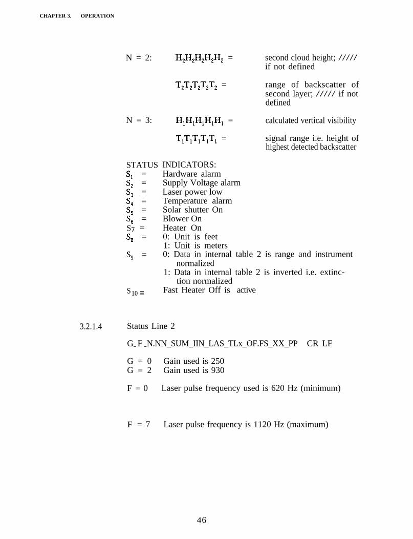
3.2.1.3 Status Line 1 (Identical in all messages)
NSB-H,H,H,H,H,-T,T,T,T,T,-H H H H H T T T T T S S S S S S S S S S2222t2222tl2345678910 CRLF
N = 0 no significant backscatter (clear air)N = 1 one layer detectedN = 2 two layers detectedN = 3 sky is fully obscured but no cloud base can be detected
from echo signal received (e.g. fog or precipitation)N = 4 sky is partially obscured and no cloud base is detected
S = 0 no alarm status bits Sl...S4 ON for more than 5 mm.at least one alarm status Sl...S4 ON for more than 5min.
B = space if S = 0
B = ‘bel’ character if S = 1. Because 'bel' is a nonprintingcharacter the alarming line appears one charactershorter in a printout than normally.
N = 0 or 4: H,=H,=T,=T,= /////
N = 1 or 2: H,H,H,H,H, =
T,T,T,TIT1 =
the lowest detected cloudheight in 5 digits. Leadingzeroes not suppressed.range of backscatter of firstlayer; ///// if not defined
45
Archive
S = 1
CHAPTER 3. OPERATION
N = 2:
N = 3:
STATUSs, =s, =s, =s, =s, =s, =S =s, =
s, =
S10 =
H*H,H,H*H, =
T,T,T,T,T, =
H,H,H,H,H, =
TIT,T,T,T1 =
second cloud height; /////if not defined
range of backscatter ofsecond layer; ///// if notdefined
calculated vertical visibility
signal range i.e. height ofhighest detected backscatter
INDICATORS:Hardware alarmSupply Voltage alarmLaser power lowTemperature alarmSolar shutter OnBlower OnHeater On0: Unit is feet1: Unit is meters0: Data in internal table 2 is range and instrument
normalized1: Data in internal table 2 is inverted i.e. extinc-
tion normalizedFast Heater Off is active
3.2.1.4 Status Line 2
G F N.NN_SUM_IIN_LAS_TLx_OF.FS_XX_PP CR LF- -
G = 0 Gain used is 250G = 2 Gain used is 930
F = 0 Laser pulse frequency used is 620 Hz (minimum)
F = 7 Laser pulse frequency is 1120 Hz (maximum)
46
Hugh Black
Hugh Black
7
CHAPTER 3. OPERATION
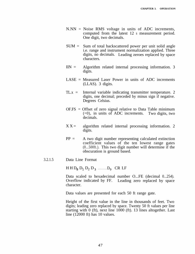
N.NN = Noise RMS voltage in units of ADC increments,computed from the latest 12 s measurement period.One digit, two decimals.
SUM = Sum of total backscattered power per unit solid anglei.e. range and instrument normalization applied. Threedigits, no decimals.characters.
Leading zeroes replaced by space
IIN = Algorithm related internal processing information. 3digits.
LASE = Measured Laser Power in units of ADC increments(LLAS). 3 digits.
TL.x = Internal variable indicating transmitter temperature. 2digits, one decimal; preceded by minus sign if negative.Degrees Celsius.
OF.FS = Offset of zero signal relative to Data Table minimum(=0), in units of ADC increments. Two digits, twodecimals.
X X = algorithm related internal processing information. 2digits.
PP = A two digit number representing calculated extinctioncoefficient values of the ten lowest range gates(0...500ft.). This two digit number will determine if theobscuration is ground based.
3.2.1.5 Data Line Format
H H D D D D . . . . . . . . D CR LF
Data scaled to hexadecimal number O...FE (decimal 0...254).Overflow indicated by FF. Leading zero replaced by spacecharacter.
Data values are presented for each 50 ft range gate.
Height of the first value in the line in thousands of feet. Twodigits; leading zero replaced by space. Twenty 50 ft values per linestarting with 0 (ft), next line 1000 (ft). 13 lines altogether. Lastline (12000 ft) has 10 values.
47
Hugh Black
9
Hugh Black
3
Hugh Black
0
Hugh Black
1
Hugh Black
2
CHAPTER 3. OPERATION
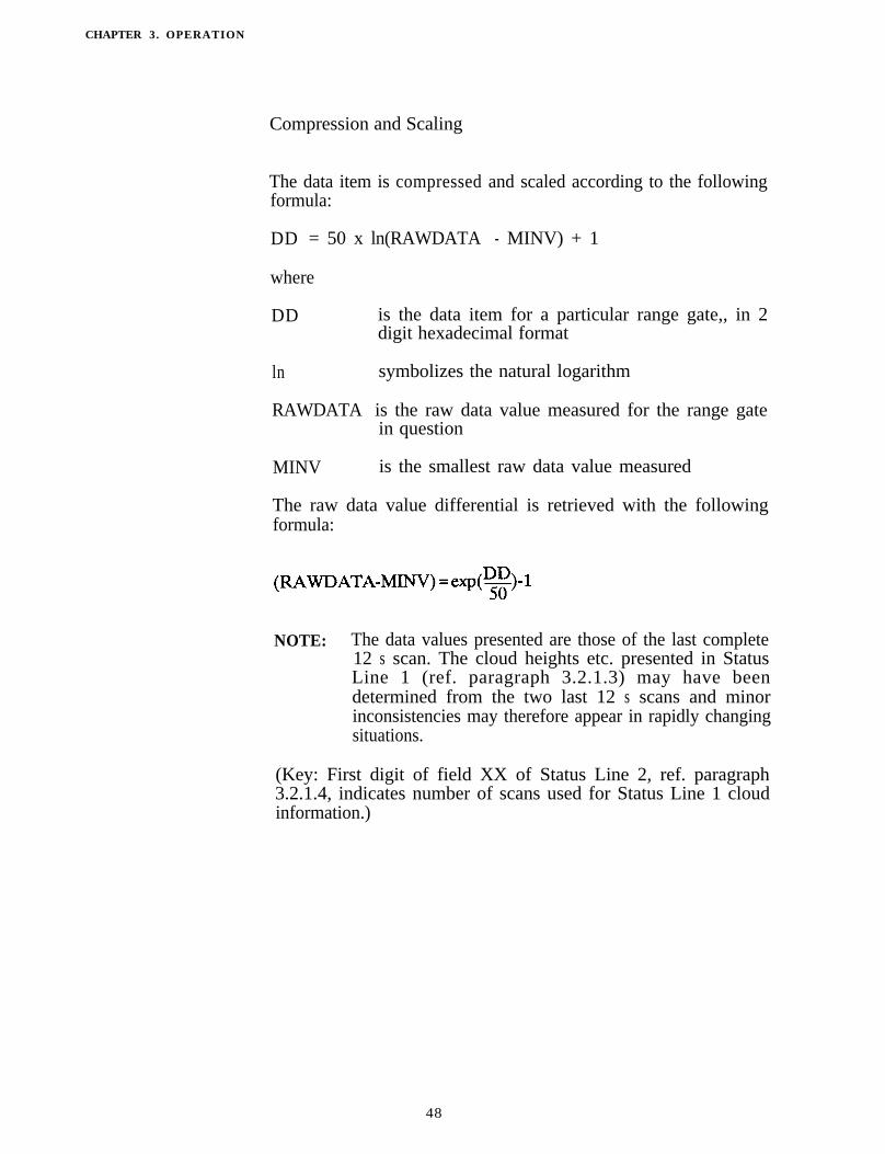
Compression and Scaling
The data item is compressed and scaled according to the followingformula:
DD = 50 x ln(RAWDATA - MINV) + 1
where
DD is the data item for a particular range gate,, in 2digit hexadecimal format
ln symbolizes the natural logarithm
RAWDATA is the raw data value measured for the range gatein question
MINV is the smallest raw data value measured
The raw data value differential is retrieved with the followingformula:
(RAWDATA-MINV)=exp(D$)-1
NOTE: The data values presented are those of the last complete12 s scan. The cloud heights etc. presented in StatusLine 1 (ref. paragraph 3.2.1.3) may have beendetermined from the two last 12 s scans and minorinconsistencies may therefore appear in rapidly changingsituations.
(Key: First digit of field XX of Status Line 2, ref. paragraph3.2.1.4, indicates number of scans used for Status Line 1 cloudinformation.)
48
CHAPTER 3. OPERATION
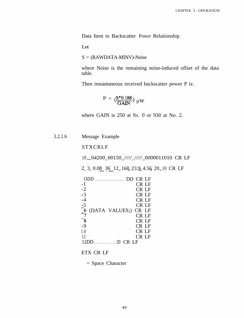
Data Item to Backscatter Power Relationship
Let
S = (RAWDATA-MINV)-Noise
where Noise is the remaining noise-induced offset of the datatable.
Then instantaneous received backscatter power P is:
P = (S*O.lSSGAIN -1 µW
where GAIN is 250 at No. 0 or 930 at No. 2.
3.2.1.6 Message Example
STXCRLF
10-04200_00150_/////_/////_0000011010 CR LF
2 3 0.08 36 12 168 23.9 4.56 20 10 CR LF- - -,- - - - - -
ODD . . . . . . . . . . . . . . . . . . . . . . . . . . . . DD CR LF-1 CR LF-2 CR LF-3 CR LF-4 CR LF-5 CR LF‘; (DATA VALUES;) CR LF
CR LF-8 CR LF-9 CR LFio CR LF11 CR LF12DD . . . . . . . . . . . . . . . . . DD CR LF
ETX CR LF
= Space Character
49
CHAPTER 3. OPERATION
3.2.2 DIGITAL MESSAGE NO. 3
3.2.2.1 General
This message contains Status Line 1 identical to Message No. 2(see 3.2.1.3) and one single range gate data line indicating thepresence or absence of backscatter in each range gate.
Message is output automatically every 12 seconds, simultaneouslywith the Gifft RBC Recorder Output (3.3) in Automatic Modewhen Line is Closed.
Activation is done with command SEND 3. This cancels anyprevious message activation; only one digital message may beactive at a time. The following is the command and Ceilometerresponse; omitting the parameter (3) will cause the currentselected message to be announced:
ST: MT:
> SEND 3(CR) > C31B3F
AUTOMATIC MESSAGE: 3 AUTO MES 3
> (next input) >_ (next input)
The Message number selection will remain in effect over aRestart or Power-Down.Message No. 3 is intended to be used with the EMOD controlparameter set to EMOD ON (see 3.3).
3.2.2.2 Format
STX CR LF<status data line l> CR LF<backscatter data line . . . > CR LF
ETX CR LF
Status Data Line 1 is identical to that of Message No. 2.
ON/OFF data is l/O accordingly. Other data is decimal orhexadecimal numbers.
50
CHAPTER 3. OPERATION
Coding is USASCII. STX, CR, LF, ETX are Start-of-Text,Carriage Return Line Feed and End-of-Text characters whichformat the message but are not visible in a printout.
Total length of message is 112 characters. Printout is 2 lines,width is max. 66 characters, whereof 64 are visible.
Time for message transmission at 300 baud is 3.73 s.
3.2.2.3 Status Line 1
Identical to that of Digital Message No. 2; see 3.2.1.3.
3.2.2.4 Backscatter Data Line
D D D D . . . . . . . . . . . . . . . . . . D CR LF
D” where n= 1 to 64 is single ASCII coded hexadecimalcharacter O...F where each bit of the 4-bit nibble ofthe hex character expressed in binary form representsone range gate.
With EMOD ON, range gate bit is 1 if Ceilometerdetermined extinction coefficient at that range gateexceeds a value corresponding to a horizontal visibilityof approx. 10 km (6 miles) except for three lowest rangegates which have higher thresholds.
D, represents the four lowest 50 ft range gates i.e. Oft,50ft, l00ft, 150ft; D, represents the four next ones i.e.200 ft, 250ft, 300ft, 350ft, etc.
0 indicates no detectable backscatter in four adjacentrange gates
F indicates backscatter in all four range gates8 indicates backscatter in the lowest range gate only1 indicates backscatter in the highest range gate only
All other characters indicate a gate-by-gate combinationof backscatter according to the binary nibble, convertedto hexadecimal.
3.2.2.5 Message Example
STX CR LF
10 04200 00150 ///// /////_0000011010 CR LFoooiFFF8@@OOO&JOOOO~AOOO . . . . ..OOO CR LF
ETXCRLF
51
Hugh Black
1
Hugh Black
3
Hugh Black
2
Hugh Black
4
Hugh Black
64
CHAPTER 3. OPERATION
3.2.3
3.2.3.1
3.2.3.2
GIFFT RBC RECORDER OUTPUT
Introduction
The CT 12K Ceilometer provides two floating non-polar outputsignal circuits for producing graphical sky condition records on aGifft RBC Recorder, operating according to the facsimileprinciple.
A new output is generated once every 12 seconds when theCeilometer is in Automatic Mode, regardless of the state of theDigital Interface (Open or Closed). In normal operation (LineClosed), output coincides once per minute with Digital MessageNo. 2 transmission start, and every time with Digital Message No.3 transmission start.
Signals
TRIGGER BREAK (Ref. RBCT)Normally-Closed relay contact that opens for 80 milliseconds asan initiation for a new output.
Doubles as an Alarm Signal by extending the break duration to200 ms when cause for Ceilorneter Fault Alarm exists. This stateis logically identical to that of bits S and B of Status Line 1 ofDigital Messages.’
CLOUD SIGNAL (Ref. RBCE)Transformer Coupled 120 Hz, signal (twice Line Frequency), on/off controlled by Ceilometer for inscribing on Recorder paper.
OPERATION AND TIMING+The Cloud Signal outputs cloud and obscuration heights as ananalog delay with respect to the trailing edge of the TriggerBreak. 0 to 12,000 ft is covered in 3 seconds, with a 20 msresolution equalling 80 ft. If the Trigger Break is 200 ms (alarm)then the reference starting point is 80 ms after the leading edgeof the Break.
52
CHAPTER 3. OPERATION
3.2.3.3 Recording Modes and Set-Up Commands
Two on/off parameters RMOD and BMOD condition the CloudSignal output:
RMOD (Recording MODe)
OFF: Only Cloud bases are recorded
ON: In addition to Cloud bases also non-cloudobscuration is recorded
BMOD (Base MODe)
OFF: Up to two cloud bases may be output duringone sweep, each with a trace duration of mm.80 ms.
ON: Only the lowest cloud base is output, and witha fixed 60 ms trace duration.
RECOMMENDED STANDARD SETTINGS ARE:
RMOD ON
BMOD OFF
53
CHAPTER 3. OPERATION
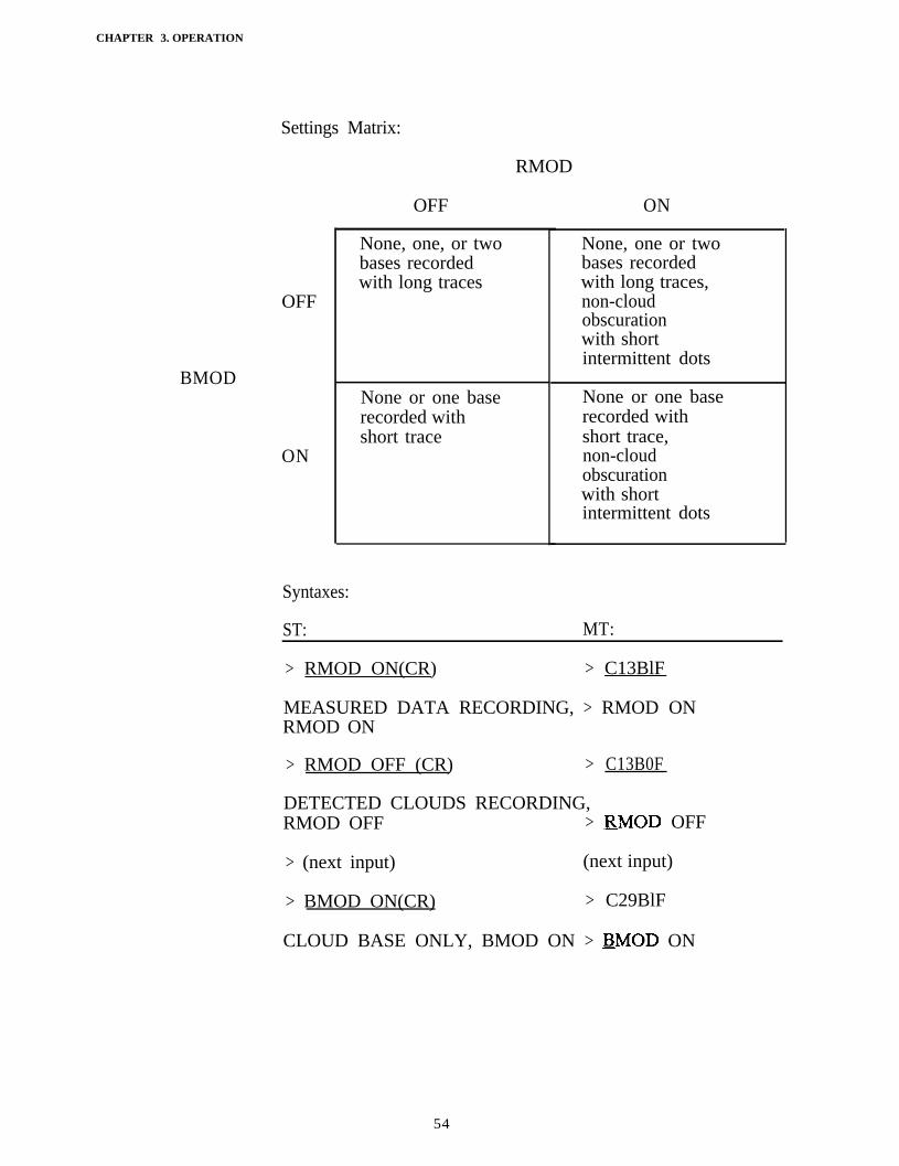
Settings Matrix:
RMOD
OFF
BMOD
ON
OFF
None, one, or twobases recordedwith long traces
None or one baserecorded withshort trace
ON
None, one or twobases recordedwith long traces,non-cloudobscurationwith shortintermittent dots
None or one baserecorded withshort trace,non-cloudobscurationwith shortintermittent dots
Syntaxes:
ST:
> RMOD ON(CR)
MT:
> C13BlF
MEASURED DATA RECORDING, > RMOD ONRMOD ON
> RMOD OFF (CR) > C13B0F
DETECTED CLOUDS RECORDING,RMOD OFF > RMOD OFF
> (next input) (next input)
> BMOD ON(CR) > C29BlF
CLOUD BASE ONLY, BMOD ON > BMOD ON
54
CHAPTER 3. OPERATION
> BMOD OFF(CR) > C29B0F
ALL CLOUD DATA, BMOD OFF > BMOD OFF
> (next input) (next input)
Settings are stored in non-volatile memory.
3.2.3.4 Examples and Interpretations
The CT 12K 0 t o 12000 ft range is linearly scaled forScaling:the Gifft RBC Recorder 0 to 90 degrees scale i.e.:
0 ft = 0 deg1000 ft = 7.5 deg12000 ft = 90 deg
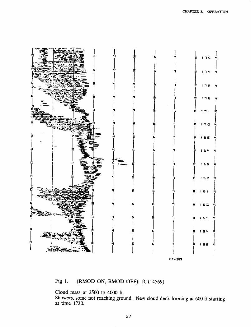
Cloud Trace:An instantaneous 12 sec. cloud hit is recorded as asolid thin line starting at the detected cloud height andextending upwards a minimum of 240 ft (60 ms) anda maximum equalling the penetration (typ. max. 400 ft).A time graph of cloud height is produced by severalsubsequent instantaneous traces.
In broken, scattered, or highly turbulent conditions in-stantaneous hit traces may be spread over a wide range,or group into several distinct cloud mass images. Visualgrouping and averaging of a longer period of the recordwill then provide a better result for reporting purposesthan instantaneous hits.
Non-Cloud ObscurationHeight ranges where backscatter has been detected andthe obstruction calculated to have a point extinctioncoefficient exceeding a value corresponding to ahorizontal visibility of approx. 6 miles (10 km) but notexceeding the cloud criteria, are marked with a greyishcloud signal in the RMOD ON recording mode.
The greyish appearance is accomplished bysemi-randomly on-off switching the cloud signal duringthe sweep, and disabling the non-cloud obscurationsignal altogether every second sweep.
55
CHAPTER 3. OPERATION
In totally obscured conditions where no cloud base isdetected the non-cloud obscuration signal will be outputup to the calculated Vertical Visibility (ceiling) height;this can then be seen in the record as the upper(higher) edge of the greyish area.
In cases of rapid changes in cloud heights and/or posi-tion, backscatter from a cloud base may be blurred overa wide range and momentarily fail to produce a reliablecloud backscatter signature. These instants will howeverat least provide a non-cloud obscuration detection toenhance the record image of the situation.
56
CHAPTER 3. OPERATION
3.3 PARAMETERS AND OPERATlON MODES
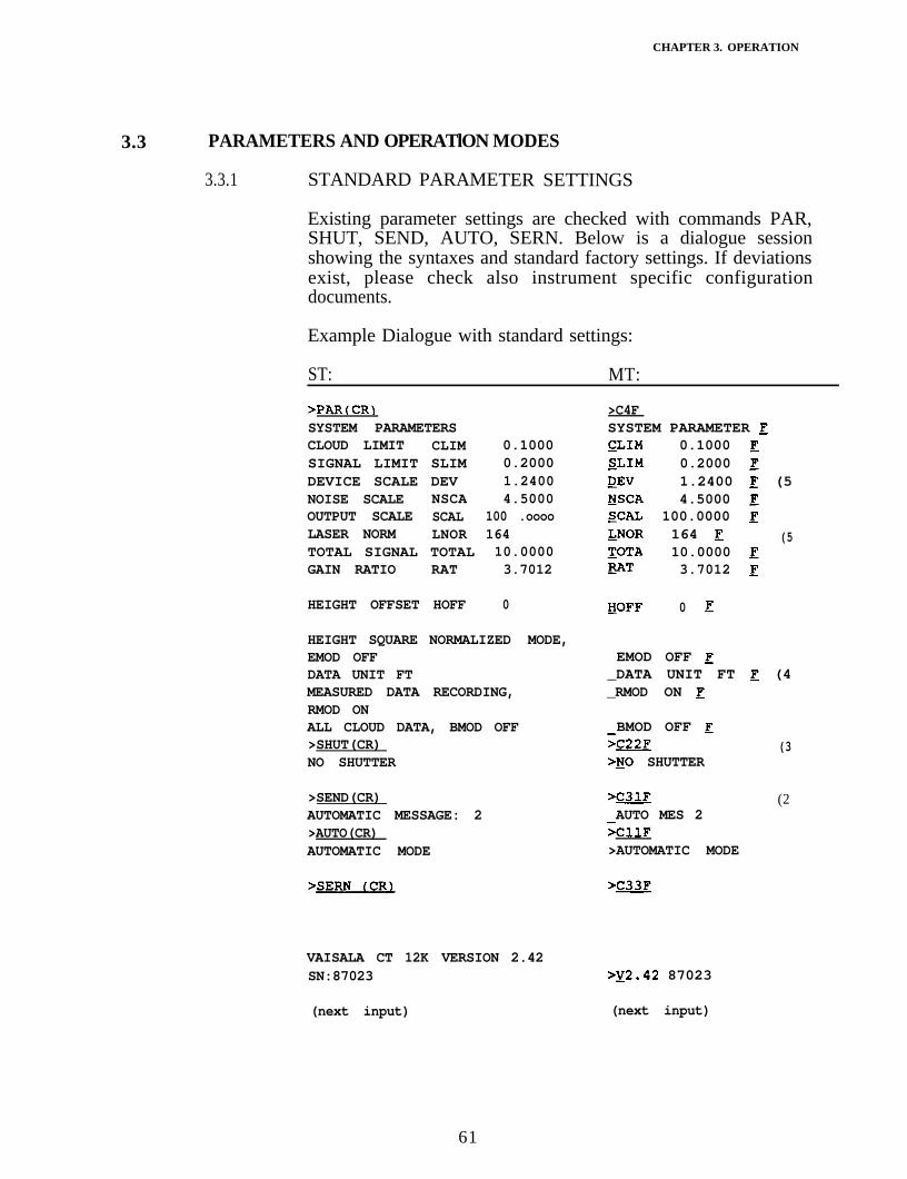
3.3.1 STANDARD PARAMETER SETTINGS
Existing parameter settings are checked with commands PAR,SHUT, SEND, AUTO, SERN. Below is a dialogue sessionshowing the syntaxes and standard factory settings. If deviationsexist, please check also instrument specific configurationdocuments.
Example Dialogue with standard settings:
ST: MT:
>PAR(C!R)SYSTEM PARAMETERSCLOUD LIMIT CLIMSIGNAL LIMIT SLIMDEVICE SCALE DEVNOISE SCALE NSCAOUTPUT SCALE SCALLASER NORM LNORTOTAL SIGNAL TOTALGAIN RATIO RAT
0.10000.20001.24004.5000
100 .oooo16410.00003.7012
HEIGHT OFFSET HOFF 0 HOFF 0 E
HEIGHT SQUARE NORMALIZED MODE,EMOD OFFDATA UNIT FTMEASURED DATA RECORDING,RMOD ONALL CLOUD DATA, BMOD OFF>SHUT(CR)NO SHUTTER
>SEND(CR) >wAUTOMATIC MESSAGE: 2 AUTO MES 2>AUTO(CR) %llFAUTOMATIC MODE >AUTOMATIC MODE
VAISALA CT 12K VERSION 2.42SN:87023
>C4FSYSTEM PARAMETER ECLIM 0.1000 ESLIM 0.2000 EDEV 1.2400 E (5NSCA 4.5000 ESCAL 100.0000 z&NOR 164 E (5TOTA 10.0000 ERAT 3.7012 g
EMOD OFF e_DATA UNIT FT E (4_RMOD ON Jf
BMOD OFF ETm>kJO SHUTTER
By2.42 87023
(next input)
(3
(2
(next input)
61
CHAPTER 3. OPERATION
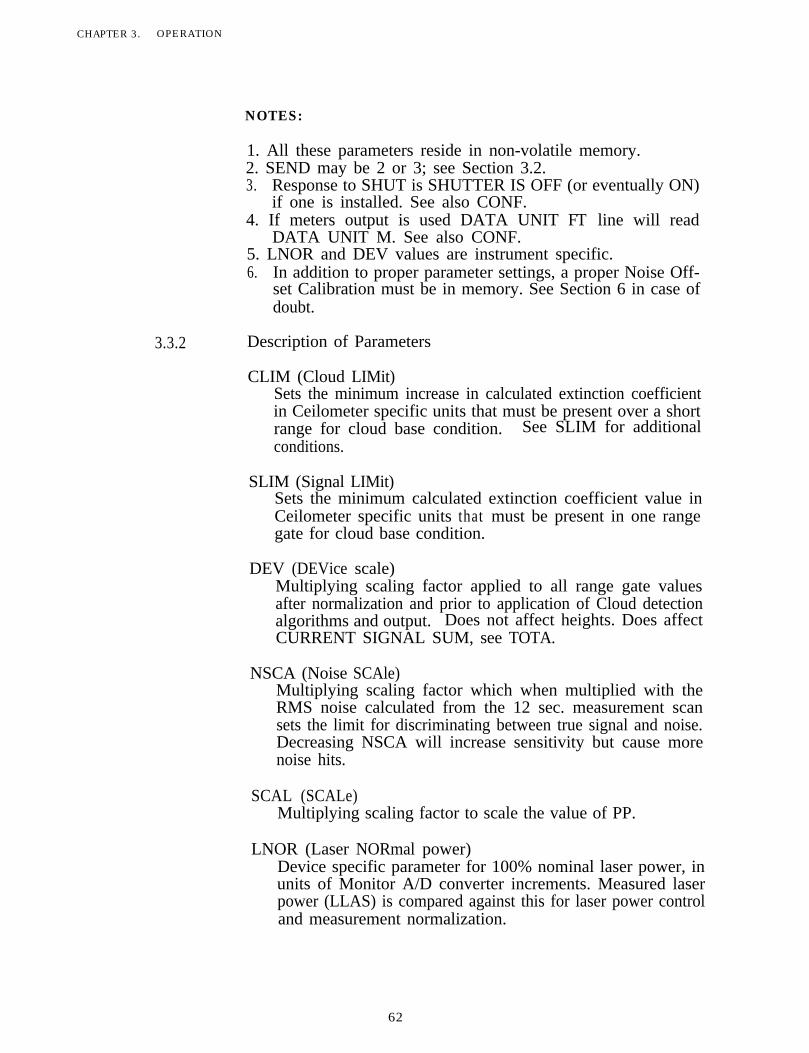
NOTES:
3.3.2
1. All these parameters reside in non-volatile memory.2. SEND may be 2 or 3; see Section 3.2.3. Response to SHUT is SHUTTER IS OFF (or eventually ON)
if one is installed. See also CONF.4. If meters output is used DATA UNIT FT line will read
DATA UNIT M. See also CONF.5. LNOR and DEV values are instrument specific.6. In addition to proper parameter settings, a proper Noise Off-
set Calibration must be in memory. See Section 6 in case ofdoubt.
Description of Parameters
CLIM (Cloud LIMit)Sets the minimum increase in calculated extinction coefficientin Ceilometer specific units that must be present over a shortrange for cloud base condition. See SLIM for additionalconditions.
SLIM (Signal LIMit)Sets the minimum calculated extinction coefficient value inCeilometer specific units that must be present in one rangegate for cloud base condition.
DEV (DEVice scale)Multiplying scaling factor applied to all range gate valuesafter normalization and prior to application of Cloud detectionalgorithms and output. Does not affect heights. Does affectCURRENT SIGNAL SUM, see TOTA.
NSCA (Noise SCAle)Multiplying scaling factor which when multiplied with theRMS noise calculated from the 12 sec. measurement scansets the limit for discriminating between true signal and noise.Decreasing NSCA will increase sensitivity but cause morenoise hits.
SCAL (SCALe)Multiplying scaling factor to scale the value of PP.
LNOR (Laser NORmal power)Device specific parameter for 100% nominal laser power, inunits of Monitor A/D converter increments. Measured laserpower (LLAS) is compared against this for laser power controland measurement normalization.
62
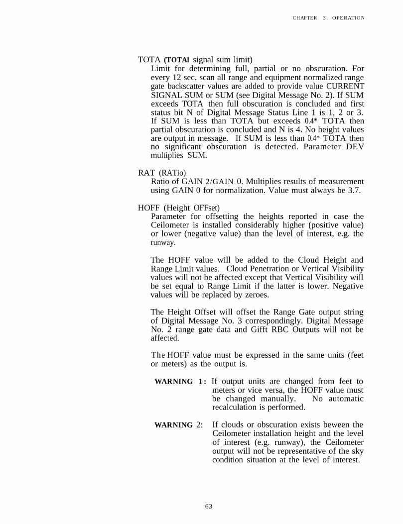
CHAPTER 3. OPERATION
TOTA (TOTAl signal sum limit)Limit for determining full, partial or no obscuration. Forevery 12 sec. scan all range and equipment normalized rangegate backscatter values are added to provide value CURRENTSIGNAL SUM or SUM (see Digital Message No. 2). If SUMexceeds TOTA then full obscuration is concluded and firststatus bit N of Digital Message Status Line 1 is 1, 2 or 3.If SUM is less than TOTA but exceeds 0.4* TOTA thenpartial obscuration is concluded and N is 4. No height valuesare output in message. If SUM is less than 0.4* TOTA thenno significant obscuration is detected. Parameter DEVmultiplies SUM.
RAT (RATio)Ratio of GAIN 2/GAIN 0. Multiplies results of measurementusing GAIN 0 for normalization. Value must always be 3.7.
HOFF (Height OFFset)Parameter for offsetting the heights reported in case theCeilometer is installed considerably higher (positive value)or lower (negative value) than the level of interest, e.g. therunway.
The HOFF value will be added to the Cloud Height andRange Limit values. Cloud Penetration or Vertical Visibilityvalues will not be affected except that Vertical Visibility willbe set equal to Range Limit if the latter is lower. Negativevalues will be replaced by zeroes.
The Height Offset will offset the Range Gate output stringof Digital Message No. 3 correspondingly. Digital MessageNo. 2 range gate data and Gifft RBC Outputs will not beaffected.
The HOFF value must be expressed in the same units (feetor meters) as the output is.
WARNING 1: If output units are changed from feet tometers or vice versa, the HOFF value mustbe changed manually. No automaticrecalculation is performed.
WARNING 2: If clouds or obscuration exists beween theCeilometer installation height and the levelof interest (e.g. runway), the Ceilometeroutput will not be representative of the skycondition situation at the level of interest.
63
CHAPTER 3. OPERATION
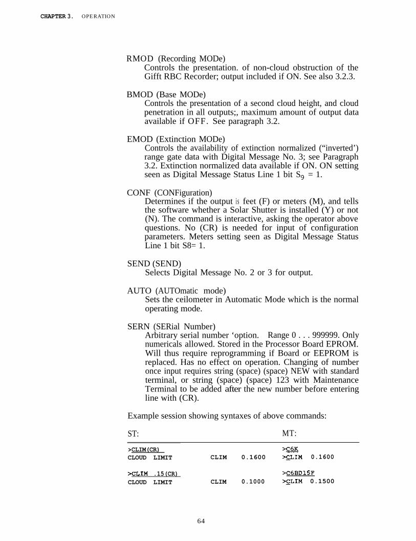
RMOD (Recording MODe)Controls the presentation. of non-cloud obstruction of theGifft RBC Recorder; output included if ON. See also 3.2.3.
BMOD (Base MODe)Controls the presentation of a second cloud height, and cloudpenetration in all outputs;, maximum amount of output dataavailable if OFF. See paragraph 3.2.
EMOD (Extinction MODe)Controls the availability of extinction normalized (“inverted’)range gate data with Digital Message No. 3; see Paragraph3.2. Extinction normalized data available if ON. ON settingseen as Digital Message Status Line 1 bit S = 1.
CONF (CONFiguration)Determines if the output is feet (F) or meters (M), and tellsthe software whether a Solar Shutter is installed (Y) or not(N). The command is interactive, asking the operator abovequestions. No (CR) is needed for input of configurationparameters. Meters setting seen as Digital Message StatusLine 1 bit S8= 1.
SEND (SEND)Selects Digital Message No. 2 or 3 for output.
AUTO (AUTOmatic mode)Sets the ceilometer in Automatic Mode which is the normaloperating mode.
SERN (SERial Number)Arbitrary serial number ‘option. Range 0 . . . 999999. Onlynumericals allowed. Stored in the Processor Board EPROM.Will thus require reprogramming if Board or EEPROM isreplaced. Has no effect on operation. Changing of numberonce input requires string (space) (space) NEW with standardterminal, or string (space) (space) 123 with MaintenanceTerminal to be added after the new number before enteringline with (CR).
Example session showing syntaxes of above commands:
ST: MT:
>CLIM(CR) x6KCLOUD LIMIT CLIM 0.1600 ->CLIM 0.1600
XLIM .15(CR) X6BD15FCLOUD LIMIT CLIM 0.1000 >CLIM 0.1500
64
Hugh Black
9
CHAPTER 3. OPERATION
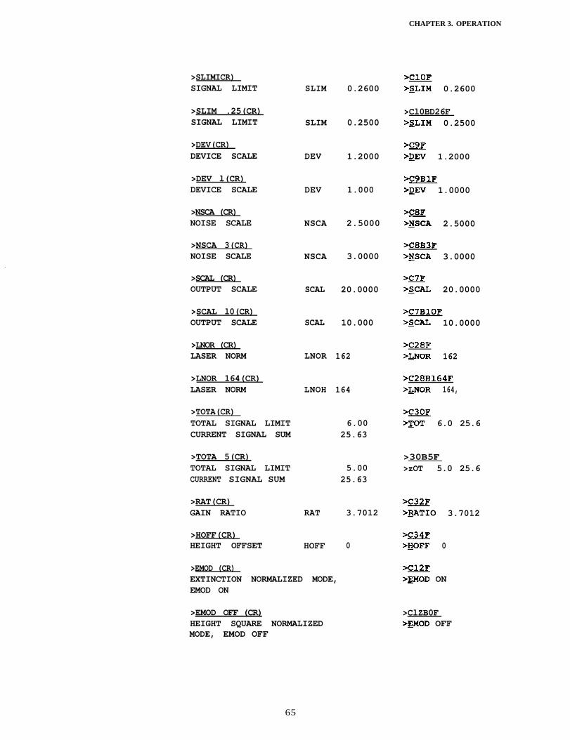
>SLIMICR)SIGNAL LIMIT
>SLIM .25(CR)SIGNAL LIMIT
>DEV(CR)DEVICE SCALE
>DEV l(CR)DEVICE SCALE
>NSCA (CR)NOISE SCALE
>NSCA 3(CR)NOISE SCALE
>SCAL (CR)OUTPUT SCALE
>SCAL l0(CR)OUTPUT SCALE
>LNOR (CR)LASER NORM
>LNOR 164(CR)LASER NORM
>TOTA(CR)TOTAL SIGNAL LIMITCURRENT SIGNAL SUM
>TOTA 5(CR)TOTAL SIGNAL LIMITCURRENT SIGNAL SUM
>RAT(CR)GAIN RATIO
>HOFF(CR)HEIGHT OFFSET
>EMOD (CR)
SLIM 0.2600
SLIM 0.2500
DEV 1.2000
DEV 1.000
NSCA 2.5000
NSCA 3.0000
SCAL 20.0000
SCAL 10.000
LNOR 162
LNOH 164
6.0025.63
5.0025.63
RAT 3.7012
HOFF 0
EXTINCTION NORMALIZED MODE,EMOD ON
>EMOD OFF (CR)HEIGHT SQUARE NORMALIZEDMODE, EMOD OFF
XlOF>SLIM 0.2600
>Cl0BD26F>SLIM 0.2500
X9F>@i 1.2000
X9BlF
>DEV 1.0000
>w>&3X4 2.5000
>C8B3FXJSCA 3.0000
>u>gziL 20.0000
>C7BlOF+XL 10.0000
>C28F>&NOR 162
>C28B164F>&NOR 164,
>QOJ>zOT 6.0 25.6
>30B5F>zOT 5.0 25.6
>w>_RATIO 3.7012
>w>HOFF 0
xmBEMOD ON
>ClZB0F>BMOD OFF
65
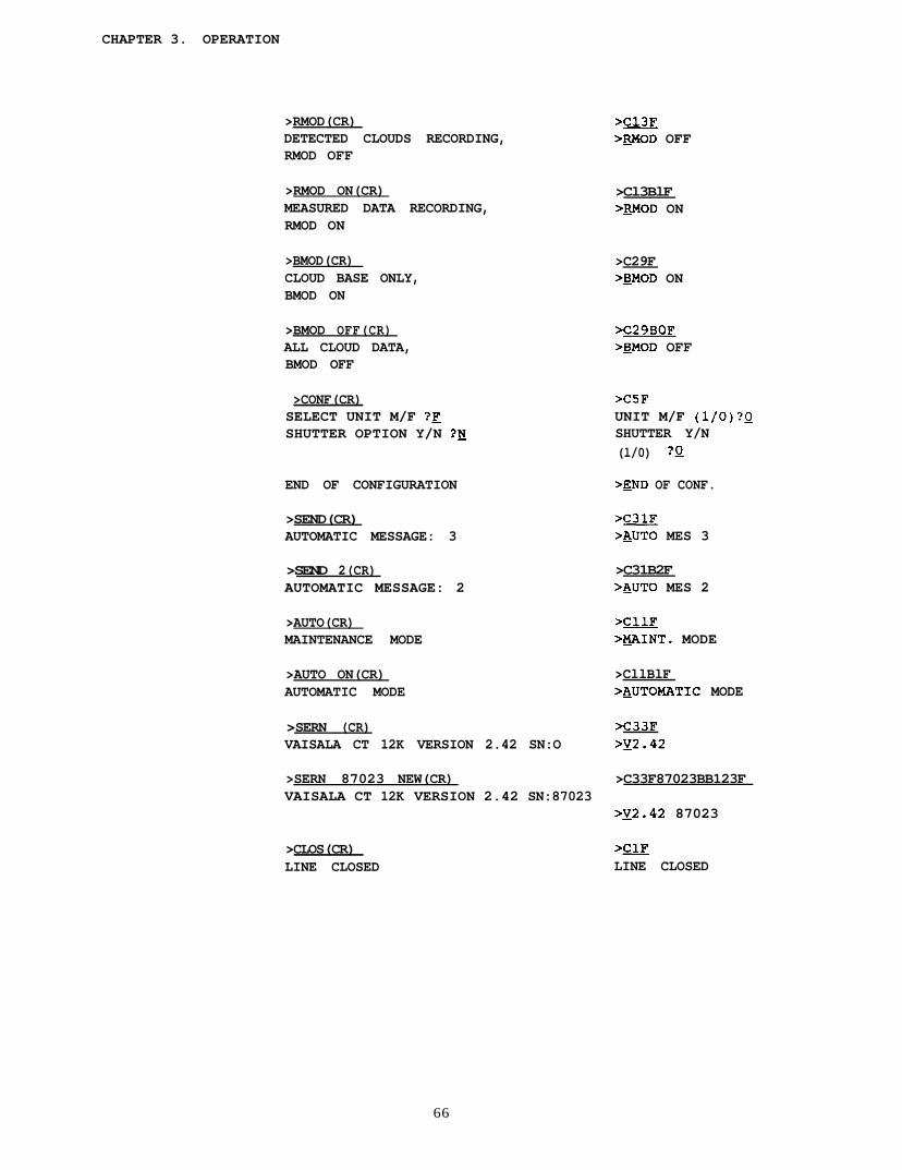
CHAPTER 3. OPERATION
>RMOD(CR) >wDETECTED CLOUDS RECORDING, >wOD OFFRMOD OFF
>RMOD ON(CR) >Cl3BlFMEASURED DATA RECORDING, >FJMOD ONRMOD ON
>BMOD(CR) >C29FCLOUD BASE ONLY, >BMOD ONBMOD ON
>BMOD OFF(CR) >C29B0FALL CLOUD DATA, >EJMOD OFFBMOD OFF
>CONF(CR) X5FSELECT UNIT M/F ?F UNIT M/F (l/O)?0SHUTTER OPTION Y/N ?N SHUTTER Y/N
(l/0) 70
END OF CONFIGURATION >END OF CONF.
>SEND(CR) >wAUTOMATIC MESSAGE: 3 >EUTO MES 3
>SEND 2(CR) >C31B2FAUTOMATIC MESSAGE: 2 >@JTO MES 2
>AUTO(CR) >wMAINTENANCE MODE XjAINT. MODE
>AUTO ON(CR) >CllBlFAUTOMATIC MODE >AUTOMATIC MODE
>SERN (CR) X33FVAISALA CT 12K VERSION 2.42 SN:O XJ2.42
>SERN 87023 NEW(CR) >C33F87023BB123FVAISALA CT 12K VERSION 2.42 SN:87023
zq2.42 87023
>CLOS(CR) >uLINE CLOSED LINE CLOSED
66
CHAPTER 3. OPERATION
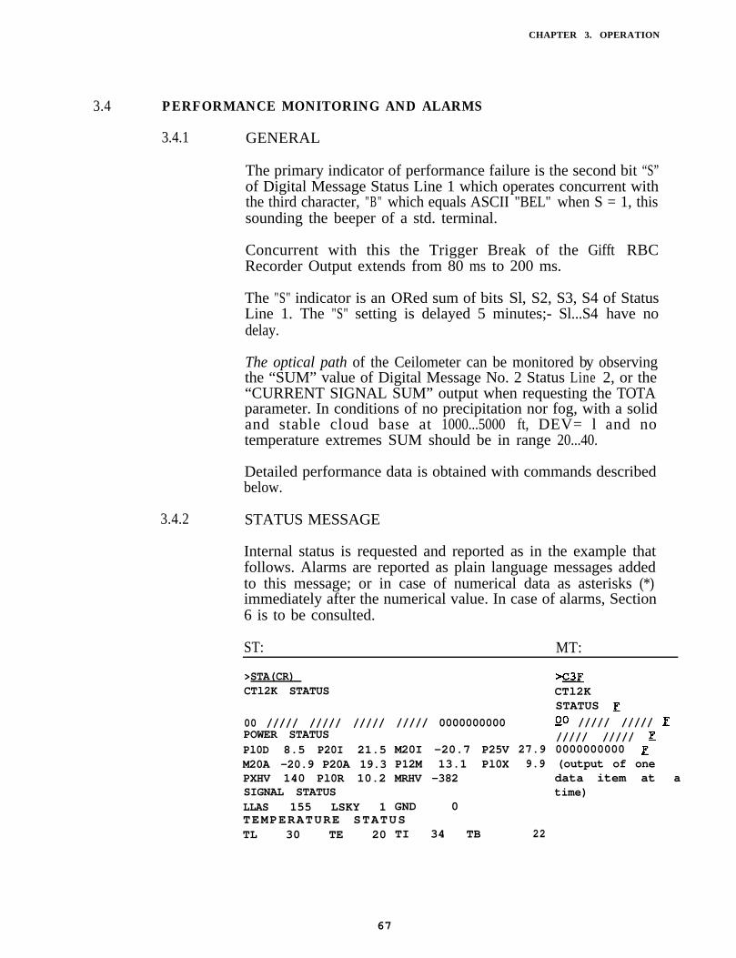
3.4 PERFORMANCE MONITORING AND ALARMS
3.4.1 GENERAL
The primary indicator of performance failure is the second bit “S”of Digital Message Status Line 1 which operates concurrent withthe third character, "B" which equals ASCII "BEL" when S = 1, thissounding the beeper of a std. terminal.
Concurrent with this the Trigger Break of the Gifft RBCRecorder Output extends from 80 ms to 200 ms.
The "S" indicator is an ORed sum of bits Sl, S2, S3, S4 of StatusLine 1. The "S" setting is delayed 5 minutes;- Sl...S4 have nodelay.
The optical path of the Ceilometer can be monitored by observingthe “SUM” value of Digital Message No. 2 Status Line 2, or the“CURRENT SIGNAL SUM” output when requesting the TOTAparameter. In conditions of no precipitation nor fog, with a solidand stable cloud base at 1000...5000 ft, DEV= l and notemperature extremes SUM should be in range 20...40.
Detailed performance data is obtained with commands describedbelow.
3.4.2 STATUS MESSAGE
Internal status is requested and reported as in the example thatfollows. Alarms are reported as plain language messages addedto this message; or in case of numerical data as asterisks (*)immediately after the numerical value. In case of alarms, Section6 is to be consulted.
ST: MT:
>STA(CR) >mCTl2K STATUS CTl2K
STATUS E
00 ///// ///// ///// ///// 0000000000 00 ///// ///// EPOWER STATUS ///// ///// EPl0D 8.5 P20I 21.5 M20I -20.7 P25V 27.9 0000000000 rM20A -20.9 P20A 19.3 P12M 13.1 Pl0X 9.9 (output of onePXHV 140 Pl0R 10.2 MRHV -382 data item at aSIGNAL STATUS time)LLAS 155 LSKY 1 GND 0TEMPERATURE STATUSTL 30 TE 20 TI 34 TB 22
67
CHAPTER 3. OPERATION
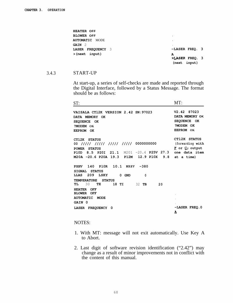
3.4.3
HEATER OFFBLOWER OFFAUTOMATIC MODEGAIN 2LASER FREQUENCY 3>(next input)
START-UP
.
.
.-LASER FREQ. 3
A>IJiSER FREQ. 3(next input)
At start-up, a series of self-checks are made and reported throughthe Digital Interface, followed by a Status Message. The formatshould be as follows:
ST: MT:
VAISALA CTl2K VERSION 2.42 SN:97023 V2.42 87023DATA MEMORY OK DATA MEMORY OKSEQUENCE OK SEQUENCE OK?MODEM OK ?MODEM OKEEPROM OK EEPROM OK
CTl2K STATUS CTl2K STATUS00 ///// ///// ///// ///// 0000000000 (forwarding withPOWER STATUS E or (2,; outputPl0D 8.5 P20I 21.1 M201 -20.4 P25V 27.3 one data itemM20A -20.6 P20A 19.3 P12M 12.9 Pl0X 9.8 at a time)
PXHV 140 Pl0R 10.1 MRHV -380SIGNAL STATUSLLAS 209 LSKY 0 GND 0TEMPERATURE STATUSTL 30 TE 18 TI 32 TB 20HEATER OFFBLOWER OFF .AUTOMATIC MODE .GAIN 0 .LASER FREQUENCY 0 -LASER FREQ.0
B
NOTES:
1. With MT: message will not exit automatically. Use Key Ato Abort.
2. Last digit of software revision identification (“2.42”) maychange as a result of minor improvements not in conflict withthe content of this manual.
68
CHAPTER 3’. OPERATION
3.4.4 ALARM LIMITS
The internal voltages, temperatures and light power levelsreported in the Status Message are monitored against AlarmLimits. Alarms are reported as asterisks (*) immediately afterthe alarming value of the Status Message.
Voltages are in volts, they produce alarms if they are less thanthe corresponding Alarm Limit (signs disregarded).
Temperatures are in degrees centigrade (Celsius). They producealarms if they exceed the corresponding Alarm Limit.
Laser Power is in units of Monitor AD Converter increments.It produces an alarm if it is less than the Alarm Limit, See alsoNote 2.
Sky Light Power Alarm Limit is of no practical significance innormal conditions since the numerical range is O-255.
Ground is monitored for self-test purposes, and produces analarm if it exceeds the Alarm Limit.
In addition the Monitor A-to-D Converter internal reference ismonitored to be 125...131, producing an “AN MONITORERROR” message if out of limits.
An Alarm Limit Message is obtained by commanding ALIM.Specific parameters are changed by adding the correspondingreference designation with standard terminal use or the numbercode of Appendix 1: “CTM 12 Monitored Parameters” withMaintenance Terminal CTH 12, and the new limit value.Interrogation of individual values is not provided.
NOTES:
1. Alarm Limit changes will not be maintained over a poweroutage or Reset but a return to default values will take placein these instances.
2. The LLAS default alarm limit is 0.7* LNOR and will thusbe individual, as is LNOR.Below are the syntaxes for the ALIM message with defaultvalues, and a specific example:
69
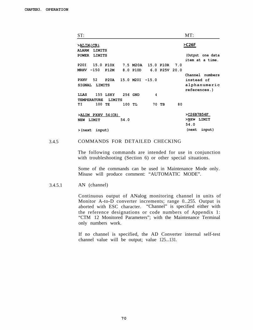
CHAPTER3. OPERATION
ST: MT:
3.4.5
3.4.5.1
>m >wALARM LIMITSPOWER LIMITS (Output one data
item at a time.P20I 15.0 Pl0X 7.5 M20A 15.0 Pl0R 7.0MRHV -150 P12M 8.0 Pl0D 6.0 P25V 20.0
Channel numbersPXHV 52 P20A 15.0 M20I -15.0 instead ofSIGNAL LIMITS alphanumeric
references.)LLAS 155 LSKY 256 GND 4TEMPERATURE LIMITSTI 100 TE 100 TL 70 TB 80
>ALIM PXHV 54(CR) >C26B7B54FNEW LIMIT 54.0 >bJEW LIMIT
54.0>(next input) (next input)
COMMANDS FOR DETAILED CHECKING
The following commands are intended for use in conjunctionwith troubleshooting (Section 6) or other special situations.
Some of the commands can be used in Maintenance Mode only.Misuse will produce comment: “AUTOMATIC MODE”.
AN (channel)
Continuous output of ANalog monitoring channel in units ofMonitor A-to-D converter increments; range 0...255. Output isaborted with ESC character. “Channel” is specified either withthe reference designations or code numbers of Appendix 1:“CTM 12 Monitored Parameters”; with the Maintenance Terminalonly numbers work.
If no channel is specified, the AD Converter internal self-testchannel value will be output; value 125...131.
70
Archive
>C26F
Archive
CHAPTER 3. OPERATION
Syntax example:
ST: MT:
>AN 8(CR) or AN LLAS(CR) >C14B8F195 195195 195195 195
.
.
. .(ESC) e>(next input) >_(next input)
.
.
3.4.5.2 LASE (on/off)
Control of Laser Enable.produces no response.
Interrogation (without ON/OFF)Control possible only in Maintenance
Mode. Requires SEQ setting for Laser trigger pukes output.The setting is automatically cleared after each measurement scan,either in Automatic Mode or a commanded one in MaintenanceMode (MEAS, CAL).
Syntax example:
>LASE ON(CR) >C15BlFLASER IS ENABLED >LASER ENABLED
>(next input) (next input)
3.4.5.3 SEQ (on/off)
Control of Measurement Sequence Enable. Interrogation (withoutON/ OFF) produces no response. Control possible only inMaintenance Mode.pulses output.
Requires LASE setting for Laser triggerThe setting is automatically cleared after each
measurement scan, either :iin Automatic Mode or a commandedone in Maintenance Mode (MEAS, CAL).
71
CHAPTER 3. OPERATION
3.4.5.4
3.4.5.5 FREQ (number)
Interrogation and setting of Laser Pulse Frequency number.Setting is possible only in Maintenance Mode.
Syntax example:
ST: MT:
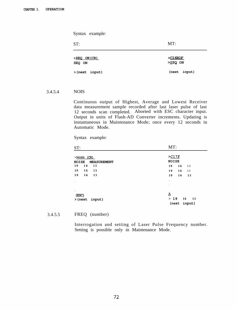
>SEQ ON(CR) >C16BlFSEQ ON >sEQ ON
>(next input) (next input)
NOIS
Continuous output of Highest, Average and Lowest Receiverdata measurement sample recorded after last laser pulse of last12 seconds scan completed. Aborted with ESC character input.Output in units of Flash-AD Converter increments. Updating isinstantaneous in Maintenance Mode; once every 12 seconds inAutomatic Mode.
Syntax example:
ST: MT:
>NOIS (CR) >mNOISE MEASUREMENT NOISE19 16 13 19 16 1 319 16 13 19 16 1 319 16 13 19 16 13
..
.
.(ESC)>(next input)
&> 19 16 13(next input)
7 2
Archive
72
Archive
CHAPTER 3. OPERATION
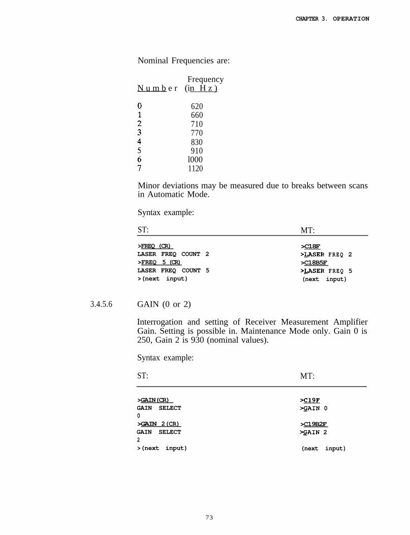
Nominal Frequencies are:
FrequencyN u m b e r (in H z )
620660710770830910
l0001120
Minor deviations may be measured due to breaks between scansin Automatic Mode.
Syntax example:
ST: MT:
>FREQ (CR) >C18FLASER FREQ COUNT 2 >&ASER FREQ 2>FREQ 5 (CR) >C18B5FLASER FREQ COUNT 5 >I&SER FREQ 5>(next input) (next input)
3.4.5.6 GAIN (0 or 2)
Interrogation and setting of Receiver Measurement AmplifierGain. Setting is possible in. Maintenance Mode only. Gain 0 is250, Gain 2 is 930 (nominal values).
Syntax example:
ST: MT:
>GAIN(CR)GAIN SELECT0>GAIN 2(CR)GAIN SELECT2>(next input)
>a>G_AIN 0
>C19B2F>GAIN 2
(next input)
73
CHAPTER 3. OPERATION
3.4.5.7
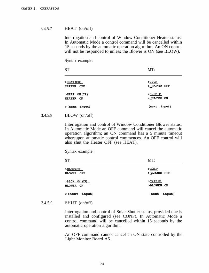
3.4.5.8 BLOW (on/off)
3.4.5.9
HEAT (on/off)
Interrogation and control of Window Conditioner Heater status.In Automatic Mode a control command will be cancelled within15 seconds by the automatic operation algorithm. An ON controlwill not be responded to unless the Blower is ON (see BLOW).
Syntax example:
ST: MT:
>HEAT(CR) >C20FHEATER OFF >HEATER OFF
>HEAT ON(CR) >C20BlFHEATER ON Z-HEATER ON
>(next input) (next input)
Interrogation and control of Window Conditioner Blower status.In Automatic Mode an OFF command will cancel the automaticoperation algorithm; an ON command has a 5 minute timeoutwhereupon automatic control commences. An OFF control willalso shut the Heater OFF (see HEAT).
Syntax example:
ST: MT:
>BLOW(CR) >C21FBLOWER OFF >EJLOWER OFF
>BLOW ON (CR). >C2lBlFBLOWER ON >BLOWER ON
>(next input) (next input)
SHUT (on/off)
Interrogation and control of Solar Shutter status, provided one isinstalled and configured (see CONF). In Automatic Mode acontrol command will be cancelled within 15 seconds by theautomatic operation algorithm.
An OFF command cannot cancel an ON state controlled by theLight Monitor Board A5.
74
CHAPTER 3. OPERATION
Syntax example:
ST: MT:
>SHUT(CR) >aSHUTTER IS OFF >SHUTTER IS OFF
>SHUT ON(CR) >C22BlFSHUTTER IS ON >SHUTTER IS ON
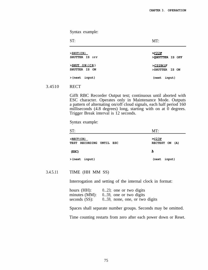
>(next input) (next input)
3.4510 RECT
Gifft RBC Recorder Output test; continuous until aborted withESC character. Operates only in Maintenance Mode. Outputsa pattern of alternating on/off cloud signals, each half period 160milliseconds (4.8 degrees) long, starting with on at 0 degrees.Trigger Break interval is 12 seconds.
Syntax example:
ST: MT:
>RECT(CR) xcTEST RECORDING UNTIL ESC RECTEST ON (A)
(ESC) li
>(next input) (next input)
3.4.5.11 TIME (HH MM SS)
Interrogation and setting of the internal clock in format:
hours (HH): 0...23; one or two digitsminutes (MM): 0...59, one or two digitsseconds (SS): 0...59, none, one, or two digits
Spaces shall separate number groups. Seconds may be omitted.
Time counting restarts from zero after each power down or Reset.
75
CHAPTER 3. OPERATION
Syntax example:
ST: MT:
>TIME(CR) x2&E00:08:19 >c24 00:08:19
>TIME 12 34(CR) >C24B12B34FTIME IS SET -24 12 34 TIME
>(next input) (next input)
3.4.5.12 DATE (YYYY MM DD)
Interrogation and setting of the internal calendar in format:
Year (YYYY): Four DigitsMonth (MM): 1...12; one or two digitsDay (DD): 1...31; one or two digits
Spaces shall separate number groups.Leap years are observed.
Date counting restarts from zero after each power down or Reset.
Syntax example:
ST: MT:
>DATE(CR) >C25F0000-00-01 >c25 0000-00-01
>DATE 1987 8 18 (CR) >C25B1987138B18DATE IS SET >c25 1987 8 18
>(next input) (next input)
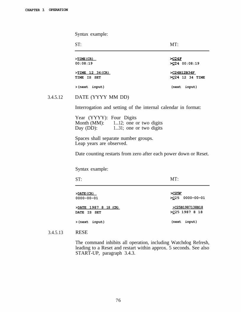
3.4.5.13 RESE
The command inhibits all operation, including Watchdog Refresh,leading to a Reset and restart within approx. 5 seconds. See alsoSTART-UP, paragraph 3.4.3.
76
CHAPTER 3. OPERATION
Syntax example:
ST: MT:
>RESET(CR)
(no-activity-delay)
>C27FX 2 7(delay)
(start-up messages) (start-up messages)
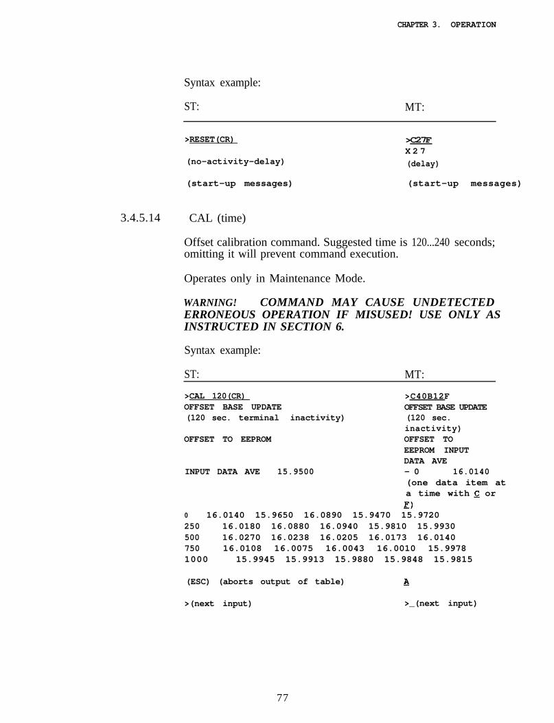
3.4.5.14 CAL (time)
Offset calibration command. Suggested time is 120...240 seconds;omitting it will prevent command execution.
Operates only in Maintenance Mode.
WARNING! COMMAND MAY CAUSE UNDETECTEDERRONEOUS OPERATION IF MISUSED! USE ONLY ASINSTRUCTED IN SECTION 6.
Syntax example:
ST: MT:
>CAL 120(CR) >C40B12FOFFSET BASE UPDATE OFFSET BASE UPDATE(120 sec. terminal inactivity) (120 sec.
inactivity)OFFSET TO EEPROM OFFSET TO
EEPROM INPUTDATA AVE
INPUT DATA AVE 15.9500 - 0 16.0140(one data item ata time with C orEl
0 16.0140 15.9650 16.0890 15.9470 15.9720250 16.0180 16.0880 16.0940 15.9810 15.9930500 16.0270 16.0238 16.0205 16.0173 16.0140750 16.0108 16.0075 16.0043 16.0010 15.99781000 15.9945 15.9913 15.9880 15.9848 15.9815
(ESC) (aborts output of table) A
>(next input) >_(next input)
77
CHAPTER 3. OPERATION
3.4.5.15 HELP
The command outputs the Standard Terminal command set withshort descriptions. No Maintenance Terminal equivalent isavailable. ESC will abort output.
Syntax example:
ST: MT:
>HELP(CR) (no equivalent)VAISALA CT 12K VERSION 2.42 SN: 87023
TIMEDATEMESPARSTACONFCLIMSLIMDEVTOTAL
NSCASCALLNOREMODRMODBMODAUTORESETLASESEQRAT
MEASHOFF
FREQNOISANGAINHEATBLOWSHUTALIMRECT
(HH MM(SS))(YYYY MM DD)AUTOMATIC DATA MESSAGEDISPLAY PARAMETERSSTATUS MESSAGESYSTEM CONFIGURATION<LIMIT> CLOUD LIMIT<LIMIT> SIGNAL LIMITSET/DISPLAY DEVICE SCALE<SIGNAL SUM> SET /DISPLAY THE NORMALIZED SIGNALSUM LIMITSET/DISPLAY NOISE SCALESET/DISPLAY OUTPUT SCALESET/DISPLAY THE LASER POWER NORMON/OFF EXTINCTION NORMALIZATIONON/OFF DATA RECORDING MODEON/OFF BASE OUTPUT ONLY ON/OFFON/OFF AUTOMATIC MODE
ON/OFF LASER ENABLE DISABLEON/OFF SEQUENCE START STOP<HIGH/LOWGAIN> SET /DISPLAY THE GAIN RATIO FORNORMALIZATION<TIME S> LASER MEASUREMENT<HEIGHT> SET/DISPLAY OFFSET VALUE FOR THEMEASURED HEIGHTS0 . . . 7 SET/DISPLAY LASER PULSE FREQUENCYSAMPLE NOISE DISPLAY0 . ..17 ANALOG TESTSELECT GAIN 0/2ON/OFF BLOWER HEATER CONTROLON/OFF BLOWER CONTROLON/OFF SOLAR SHUTTER MANUAL CONTROL<ID><VALUE> SET/DISPLAY ALARM LIMITSRECORDER TEST OUTPUT UNTIL ESC
78
CHAPTER 3. OPERATION
3.4.5.16 MEAS (time)
Performs a measurement using the specified time for sampling.If no time is specified, 1 second is used.
The command can only be used in Maintenance Mode.
After measurement completion, the raw range gate data valuesare available in Table 0 (see TAB). No further processing isperformed.
Syntax example:
ST: MT:
X4EAS 12BACK SCATTERED POWER(12 sec. terminal inactivity)INPUT DATA AVE 15.9488
(no equivalent)
>(next input)
3.4.5.17 TAB n (si ci)
Output of internal data tables, where:
n is table number as follows:
0 is raw receiver data in Flash AD converter units
1 is intermediate calculation table
2 is final range and instrument normalized data values if EMODis OFF
&al extinction normalized (inverted) data values if EMODis ON
3 is static offset data table
4 is instrument-only normalized data table
si is Start Index, 0...253, equalling the 50 ft range gate number,from which output starts. If not specified, 0 is used (= 0 ft).
79
CHAPTER 3. OPERATION
ci is Cycling Index, 1...254, equalling the number of range gatesdesired for cyclic, continuous output. If not specified, outputwill be once only, from Start Index to end of table. Ifspecified then Start Index. must also be specified, and outputcycles continuously until aborted with ESC.
Output and recycle of table starts with latest cloud heights andpenetration in the form in Digital Message Status Line 1. Non-cloud obstruction heights are not indicated.
Output line contains height of first sample in line, followed byfive samples.
Syntax example:
ST: MT:
>TAB 3 17 13(CR) (no equivalent)LASER PULSE COUNT 10907
///// ///// ///// /////850 16.0043 16.0010 15.9978 15.9945 15.99131100 15.9880 15.9848 15.9815 15.9783 15.97501350 15.9745 15.9740 15.9735
///// ///// ///// /////850 16.0043 16.0010 15.9978 15.9945 15.99131100 15.9880 15.9848 15.9815 15.9783 15.97501350 15.9745 15.9740 15.9735
///// ///// ///// /////850 16.0043 16.0010 15.9978 15.9945 15.9913
(ESC)>(next input)
3.4.5.18 GRAP n (SC si ic)
Command for semigraphic output of internal measurement data,i.e. same as with TAB, where:
n is table number, see TAB
SC is Scaling Factor for specifying how many horizontal characterpositions shall equal a value of 1.0000 in the table inquestion. If not specified, 200 is used.
si is Start Index, 0...253 i.e. first range gate number of output.If not specified, then 10 is used (=500 feet).
80
CHAPTER 3. OPERATION
ic is Index Count, 0...254 i.e. how many 50 foot range gates shallbe output. If not specified then output will be to end ofrange.
Output is once only; n o cycling is available. Comrnandparameters may be omitted from the end of the line, but not inbetween. Output may be aborted with an ESC character.
Range gate data is output one gate per line, starting from theStart Index; each line contains the height points, one per characterposition, and an asterisk (*) as a mark for the data value of thatrange gate.
Syntax example:
ST: MT:
>GRAP 0 100 0 12(CR)0 *.......
50 *100 ..............*150 *200 ....*
(no equivalent)
250 .......*300 ..............*350 ..............*400 ....*450 ....*500 .......*550 .........*
>(next input)
3.4.5.19 MES
For output of Digital Message No. 2 in the Dialog Mode (LINEOPEN).
In AUTOMATIC MODE the message will be that of the lastcompleted measurement; this operates continuously in thebackground in spite of automatic message transmission beinginhibited.
In MAINTENANCE MODE a correctly formatted message willbe output but only internal monitoring data will be updated.Additionally if a MEAS command (3.4516) is carried out, theraw range gate data table will be updated.
81
CHAPTER 3. OPERATION
With Maintenance Terminal CTH 12 the output of Status Lines1 and 2 will be in groups of max. 16 characters, and range gatecontents will be output one gate at a time, preceded by the rangeheight in feet or meters. Message viewing is controlled byForward (F), Backward (B), Continuous (C; stepping) and Abort(A) keys.
Syntax example:
ST: MT:
>MES(CR)
10 04200 00150 ///// ///// ~3000011010
2 3 0.08 36 12 168 23.9 4.56 20
-ODD.............................DD-1-2-3-4-5-6 (DATA VALUES)-7-8-91011l2DD.............DD
>(next input)
xc
10 04200 00150 E
///// ///// E0000011010 E2 3 0.08 3 6 E12 168 E23.9 4.56 20 E
0 (Data Value) E50 (Data Value) E
etc. to
12450 (Data Value)&
> (next input)
3.5 OPERATION WITH MAINTENANCE TERMINAL CTH 12
3.5.1 GENERAL
The Maintenance Terminal CTH 12 is connected to the CT 12KCeilometer through the Maintenance Terminal connector J4 atthe Equipment base bottom.
The Terminal is controlled with the hexadecimal keyboardincorporated in the terminal. The decimal number keyis (0...9)are used in entering number data; the alphabetic keys (A...F) havespecial functions:
82
CHAPTER 3. OPERATION
A key 1. message viewing ABORT DISPLAY key
B key 1. blank character (= “space”)2. message viewing BACK STEP key
C key 1. command header2. message viewing CONTINUOUS DISPLAY key
D key 1. decimal point
E key 1. minus sign
F key 1. open line2. line feed, command line terminator (= “return”)3. message viewing FORWARD STEP key
The operation of the C T 12K can be monitored/controlled bygiving commands from the Maintenance Terminal CTI-I 12. Thecommands are identified by header key (C) and commandnumbers. The correspondence of the number and commands isfound in table 3.5.3. A label inside the cover of the C T H 12Terminal includes operating instructions and a command list.
The use of commands and the command format is described inSections 3.3 and 3.4.
3.5.2 OPERATION
3.5.2.1 Opening and Closing the Line (F key, Cl command)
The system indicates being ready to accept commands byoutputting a prompt (” > “) to the LCD display of the terminal.
After being connected to the CT 12K, the terminal display isclear. This indicates that the system is not ready for commands.The communication line is opened by pressing the F key. Thesystem responds by displaying the prompt (” > " ) .
NOTE! If the system is outputting the automatic messagewhen the CTH 12 is connected, some characters mayappear in the display; and the line is not openeduntil the output is finished.
Similarly, the line should be closed when the command sessionis over so that the standard data message will be received.
83
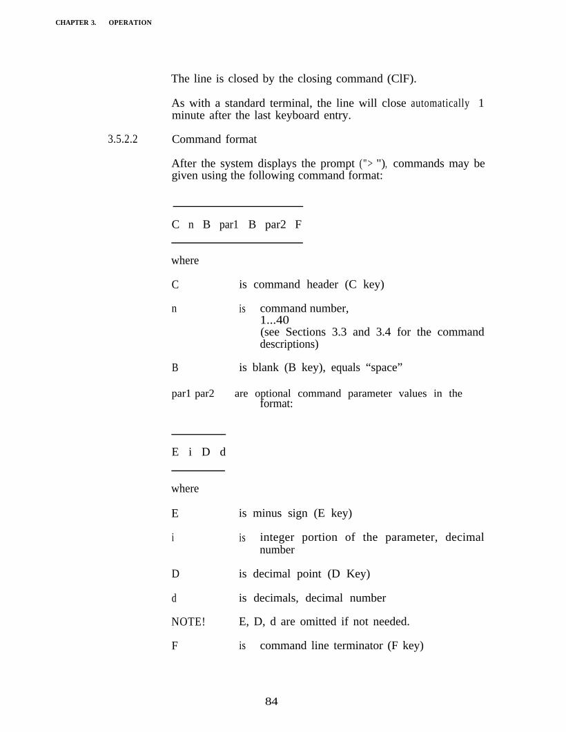
CHAPTER 3. OPERATION
The line is closed by the closing command (ClF).
3.5.2.2
As with a standard terminal, the line will close automatically 1minute after the last keyboard entry.
Command format
After the system displays the prompt ("> "), commands may begiven using the following command format:
C n B par1 B par2 F
where
C is command header (C key)
n is command number,1...40(see Sections 3.3 and 3.4 for the commanddescriptions)
B is blank (B key), equals “space”
par1 par2 are optional command parameter values in theformat:
E i D d
where
E
i
is minus sign (E key)
is integer portion of the parameter, decimalnumber
D is decimal point (D Key)
d is decimals, decimal number
NOTE! E, D, d are omitted if not needed.
F is command line terminator (F key)
84
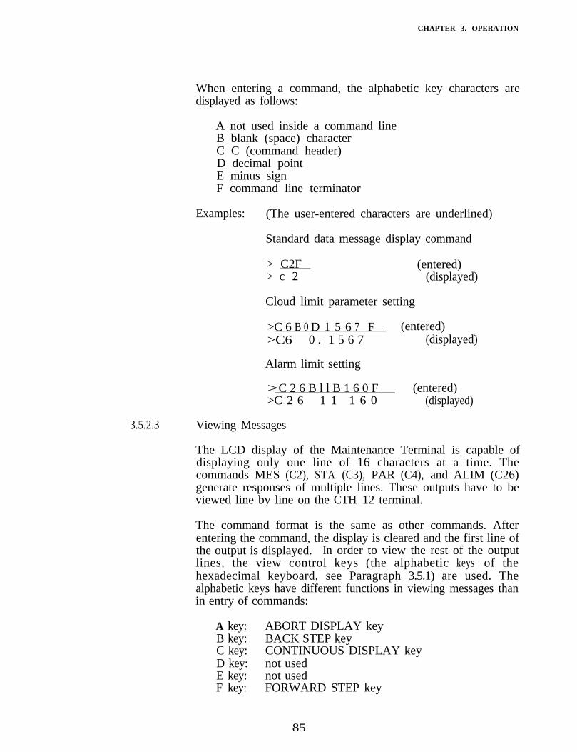
CHAPTER 3. OPERATION
When entering a command, the alphabetic key characters aredisplayed as follows:
A not used inside a command lineB blank (space) characterC C (command header)D decimal pointE minus signF command line terminator
Examples: (The user-entered characters are underlined)
Standard data message display command
> C2F (entered)> c 2 (displayed)
Cloud limit parameter setting
>C 6 B 0 D 1 5 6 7 F (entered)>C6 0 . 1 5 6 7 (displayed)
Alarm limit setting
>C 2 6 B l l B 1 6 0 F (entered)>C 2 6 1 1 1 6 0 (displayed)
3.5.2.3 Viewing Messages
The LCD display of the Maintenance Terminal is capable ofdisplaying only one line of 16 characters at a time. Thecommands MES (C2), STA (C3), PAR (C4), and ALIM (C26)generate responses of multiple lines. These outputs have to beviewed line by line on the CTH 12 terminal.
The command format is the same as other commands. Afterentering the command, the display is cleared and the first line ofthe output is displayed. In order to view the rest of the outputlines, the view control keys (the alphabetic keys of thehexadecimal keyboard, see Paragraph 3.5.1) are used. Thealphabetic keys have different functions in viewing messages thanin entry of commands:
A key: ABORT DISPLAY keyB key: BACK STEP keyC key: CONTINUOUS DISPLAY keyD key: not usedE key: not usedF key: FORWARD STEP key
85
CHAPTER 3. OPERATION
3.5.2.4
1.
2.
3.
4.
ABORT DISPLAY (A key) is used to stop the output andreturn to the ready state (prompt (” > ") is displayed whenready).
BACK STEP (B key) is used to display the previous line ofthe message (one line per key stroke).
FORWARD STEP (F key) is used to display the next lineof the message (one line per key stroke).
CONTINUOUS DISPLAY (C key) is used to display theoutput continuously line by line.
BACK STEP or FORWARD STEP key determines the directionof the continuous display. If BACK STEP is pressed prior toCONTINUOUS DISPLAY, the output advances backward; ifFORWARD STEP is pressed prior to CONTINUOUS DISPLAY,the output advances forward.
Operating Session
The use of the Maintenance Terminal CTH 12 can be dividedinto three phases:
1. Open the communication line for commands.
2. Use the commands for CT 12K operation monitoring orparameter setting.
3. Close the communication line to return to normal operation.
The CT 12K ignores operator inputs unless the communicationline is opened for commands,,
The user should close the line after each session. The line isclosed automatically after a l-minute time out period if nocharacters have been entered. Before closing the line, the systemmust be set to the proper operating mode (AUTO ON). If thesystem is left in Maintenance Mode (AUTO OFF), the automaticstandard message output is inhibited.
Some of the commands can be used only in Maintenance Mode(Section 3.5).
86
CHAPTER 3. OPERATION
3.53 COMMANDS TABLE
The commands available for the Maintenance Terminal are inthe following table. Several commands that can be entered froma standard RS-232C data terminal have been omitted from theMaintenance Terminal command set. The TAB, GRAP, andMEAS, commands are not necessary for maintenance andtroubleshooting.
The commands are identified with the command numlbers insteadof command abbreviations that are used with a standard dataterminal.
In the table are listed: o command numbero parameter(s) - if neededo corresponding abbreviation used with
standard data terminal (refer toSection 3.3)
Command Table
o description of the commando notes on use of the command
NUMBER PARAM1 PARAM2 ABBR. DESCRIPTION
Cl
C2
C3
C4
C5
------
------
------
------
------
C6 <value>
C7 <value>
C8 <value>
C9
Cl0
<value>
<value>
------
------
------
------
------
------
------
------
------
------
CLOS Close line
MES Data message display
STA Status meesage display
PAR Parameter message display
CONF Configure unit (M/F) (l/O)shutter
CLIM
SCAL
NSCA
DEV
SLIM
Cloud limit parameter set/ display
Output scale parameter set/ display
Noise scale parameter Bet/ display
Device scale parameter set/ display
Signal limit parameter set/ display
87
CHAPTER 3. OPERATION
Automatic mode ON/OFFCl1 <l/0>
Cl2 <l/0>
- - - - - - AUTO
------ EMOD Extinction normalizationON/OFF
------ RMOD
------ AN
Record Data (1) Clouds (0)Cl3 <l/0>
Cl4 <chan> Analog channelmonitoring untilaborted (2
Laser ON/OFF (1Cl5 <l/0>
Cl6 <l/0>
Cl7 ------
------ LASE
------ SEQ
------ NOIS
Sequence ON/OFF (1
Noise value monitoringuntil aborted (2
Laser frequencyset / display
Cl8 <value> FREQ
Gain set / displayCl9
C20
<0/2>
<l/0>
------ GAIN
------ HEAT Window conditioner heaterON/OFF
------ BLOW Window conditioner blowerON/OFF
C21 <l/0>
------ SHUT
------ RECT
Solar shutter ON/OFFc22 <l/0>
C23 ----- Recorder ouputtest until aborted (l&2
Time Set /DisplayHH MM (SS)
C24 <time> ------ TIME
------ DATE Date Set /Display YYYY MMDD
C25 <date>
Alarm limit set / displayC26 <chan>
C27 ------
C28 <value>
<limit> ALIM
------ RESET
------ LNOR
CPU Reset
Laser normal power parameterset /display
Base only output ON/OFF------ BMOD
------ TOTA
C29
C30
<l/0>
<value> Total parameter set /display current signal sum/ display
88
CHAPTER 3. OPERATION
C31 <value> ------ SEND
C32 <value>
C33 <value>
C34 <value>
C40 <value>
------
------
------
------
RAT
SERN
HOF'F
CAL
Digital message no select/ display
Gain Ratio Set/Display
Serial Number Set/Display
Height Offset Set/Display
Offset calibration, secl
Notes: (1 can be used only in maintenance mode
(2 abort display with A key
89
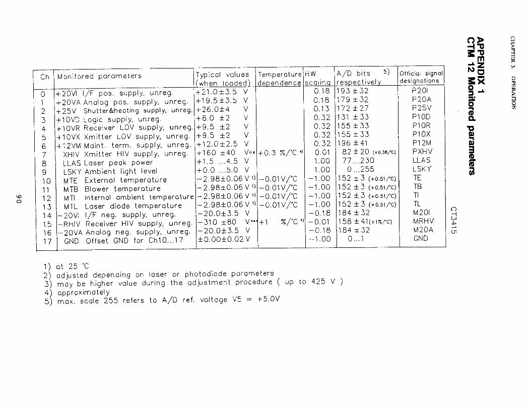

91

92
CHAPTER 4. FUNCTIONAL DESCRIPTIONTABLE OF CONTENTS
SECTION PAGE
4.1 OPERATION PRINCIPLES 97
4.2 TECHNICAL DESCRIPTION 102
4.2.1 GENERAL OUTLINE 102
4.2.2 OPERATIONAL OUTLINE 103
4.2.2.1 Measurement Circuit 1034.2.2.2 Output Interfaces 1094.2.2.3 Internal Temperature Control 1134.2.2.4 Internal Monitoring 1144.2.2.5 Power Supply Section 1144.2.2.6 Solar Shutter Option 1144.2.2.7 Window Conditioner 115
4.6.3 DRAWINGS
Wiring Diagram CT 1104Generation Breakdown Chart CT 2101Block Diagram CT 2295General Layout A.CT 3400Internal Layout, Front View A.CT 3401Internal Layout, Rear View A.CT 3402Internal Layout,Right-Hand View A.CT 3403Internal Layout,Left-Hand View A.CT 3404Internal Layout,Top View A.CT 3405Internal Layout,Bottom View A.CT 3406
117119120121122123
124
125
126
127
93
4.3 MODULE DESCRIPTIONS
4.3.1 PROCESSOR BOARD - CTM 12 REF. Al
4.3.1.14.3.1.24.3.1.34.3.1.44.3.1.4.14.3.1.4.24.3.1.4.34.3.1.4.44.3.1.54.3.1.6
GeneralSpecificationsGeneral OverviewFunctional DescriptionCPU SectionMonitor SectionSequence Control SectionAmplifier SectionParts ListDrawingsJumpers and Connections CT 4407Main Functionsand Primary Data/ControlFlow CT 4532Principal Block Diagram CT 3501Circuit Diagram l/4 CT 3385Circuit Diagram 2/4 CT 3386Circuit Diagram 3/4 CT 3387Circuit Diagram 4/4 CT 3388CPU Cycle Timing CT 3544Components Layout CT 2492Timing Diagram CT 3536
128130137138138140144148152
157
158159160161162163164165166
REFERENCES:
1 MCS-5 1 Family of Single-Chip MicrocomputersUser’s Manual, Intel Corporation, 1981.
4.3.2 UNREGULATED POWER SUPPLY BOARD CTS 12 REF. A2
4.3.2.14.3.2.24.3.2.34.3.2.44.3.2.5
IntroductionSpecificationsFunctional DescriptionParts ListDrawingsCircuit DiagramComponents Layout
167167169172
CT 3196 173CT 2294 174
94
4.3.3 OUTPUT INTERFACE REF. A3
4.3.3.14.3.3.24.3.3.34.3.3.44.3.3.5
IntroductionSpecificationsFunctional DescriptionParts ListDrawingsCircuit DiagramComponents Layout
175175176181
CT 2277 183C.CT 3278 184
REFERENCES
Technical Note “MM 74HC942 300 Baud Modem”.
4.3.4 LIGHT MONITOR BOARD CTL 13 REF. AS
4.3.4.14.3.4.24.3.4.34.3.4.44.3.4.5
IntroductionSpecificationsFunctional DescriptionParts ListDrawingsCircuit Diagram CT 3564Component Layout CT 3560CTL 13 Assembly kc-l- 3410
4.3.5 RECEIVER BOARD CTR 13 REF. A6
4.3.5.14.3.5.24.3.5.34.3.5.44.3.5.5
IntroductionSpecificationsFunctional DescriptionParts ListsDrawingsCircuit Diagram CT 3593Components Layout CT 3596Temperature Dependence CT 4594
4.3.6 TRANSMITTER BOARD CTT 12 REF. A7
4.3.6.14.3.6.24.3.6.34.3.6.44.3.6.5
IntroductionSpecificationsFunctional DescriptionParts ListDrawingsLaser Diode Temperature Curve/TP3 Voltage Curve CT 4417Circuit Diagram CT 3120Components Layout CT 2210
185185186189
190191192
193194195197
199200201
202202203208
206210211
95
4.3.7 HIGH-VOLTAGE POWER SUPPLY CTP 12 REF. PSl
4.3.7.1 Introduction4.3.7.2 Specifications4.3.7.3 Functional Description4.3.7.4 Parts List4.3.7.5 Drawings
Circuit Diagram C T 3289Wiring Drawing U.CT 1200Al Components Layout CT 3207
4.3.8 WINDOW CONDITIONER 2736 REF. Bl
4.3 .8 .1 In t roduc t ion4 .3 .8 .2 Spec i f ica t ion4.3.8.3 Functional Description4.3.8.4 Parts List4.3.8.5 Drawings
Circuit Diagram CT 4290Heater SubassemblyDrawing U.CT 1300Blower SubassemblyDrawing U.CT 2311
4.3.9 MAINTENANCE TERMINAL CTH 12
4.3 .9 .1 In t roduc t ion4.3.9.2 Specifications4.3.9.3 Functional Description4.3.9.4 Parts Lists4.3.9.5 Drawings
Block DiagramCircuit DiagramComponents Layout
A.CT 3416CT 2284
C.CT 3493
213213215217
220221223
225225226228
229
230
231
232232234249
253254255
96
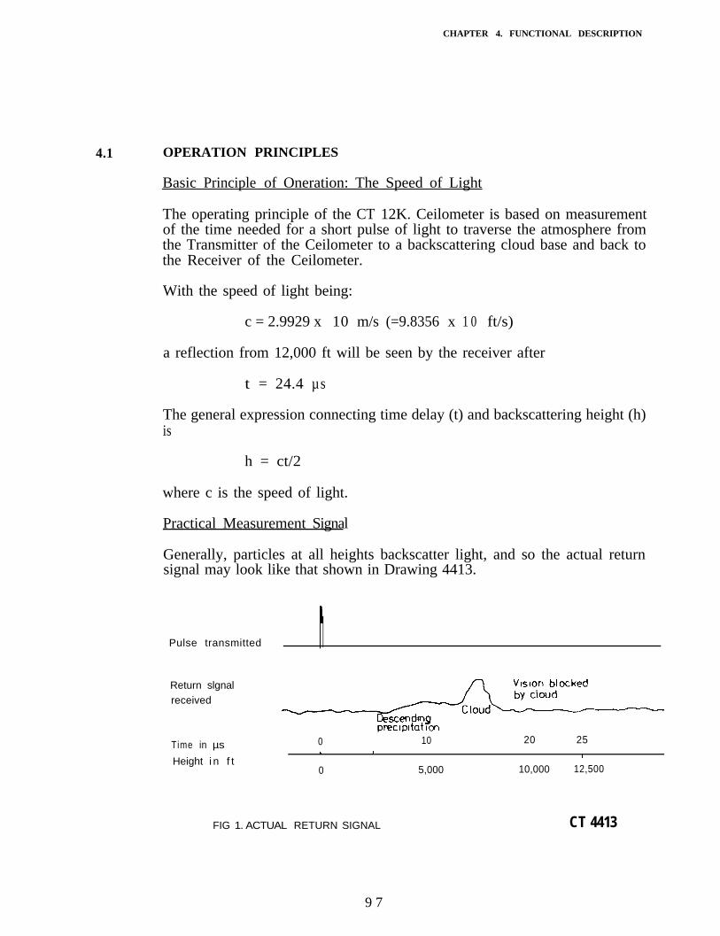
CHAPTER 4. FUNCTIONAL DESCRIPTION
4.1 OPERATION PRINCIPLES
Basic Principle of Oneration: The Speed of Light
The operating principle of the CT 12K. Ceilometer is based on measurementof the time needed for a short pulse of light to traverse the atmosphere fromthe Transmitter of the Ceilometer to a backscattering cloud base and back tothe Receiver of the Ceilometer.
With the speed of light being:
c = 2.9929 x 10 m/s (=9.8356 x 1 0 ft/s)
a reflection from 12,000 ft will be seen by the receiver after
t = 24.4 µs
The general expression connecting time delay (t) and backscattering height (h)is
h = ct/2
where c is the speed of light.
Practical Measurement Signal
Generally, particles at all heights backscatter light, and so the actual returnsignal may look like that shown in Drawing 4413.
Pulse transmitted
Return slgnal
received
Time in µs
Height i n f t
I
0 10 20 251 1 1
0 5,000 10,000 12,500
FIG 1. ACTUAL RETURN SIGNAL CT 4413
9 7
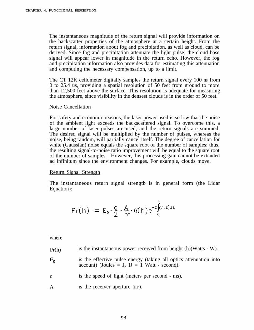
CHAPTER 4. FUNCTIONAL DESCRIPTION
The instantaneous magnitude of the return signal will provide information onthe backscatter properties of the atmosphere at a certain height. From thereturn signal, information about fog and precipitation, as well as cloud, can bederived. Since fog and precipitation attenuate the light pulse, the cloud basesignal will appear lower in magnitude in the return echo. However, the fogand precipitation information also provides data for estimating this attenuationand computing the necessary compensation, up to a limit.
The CT 12K ceilometer digitally samples the return signal every 100 ns from0 to 25.4 us, providing a spatial resolution of 50 feet from ground to morethan 12,500 feet above the surface. This resolution is adequate for measuringthe atmosphere, since visibility in the densest clouds is in the order of 50 feet.
Noise Cancellation
For safety and economic reasons, the laser power used is so low that the noiseof the ambient light exceeds the backscattered signal. To overcome this, alarge number of laser pulses are used, and the return signals are summed.The desired signal will be multiplied by the number of pulses, whereas thenoise, being random, will partially cancel itself. The degree of cancellation forwhite (Gaussian) noise equals the square root of the number of samples; thus,the resulting signal-to-noise ratio improvement will be equal to the square rootof the number of samples. However, this processing gain cannot be extendedad infinitum since the environment changes. For example, clouds move.
Return Signal Strength
The instantaneous return signal strengtb is in general form (the LidarEquation):
where
Pr(h)
Eo
C
A
is the instantaneous power received from height (h)(Watts - W).
is the effective pulse energy (taking all optics attenuation intoaccount) (Joules = J, 1J = 1 Watt - second).
is the speed of light (meters per second - ms).
is the receiver aperture (m²).
98
CHAPTER 4. FUNCTIONAL. DESCRIPTlON
h is the height in question (m).
ß(h) is the volume backscatter coefficient at height h (m-’ sr-I, sr =steradian).
h
e-2J0(z)dzis the atmospheric transmittance and accounts forthe transmitted and backscattered power by extinction (z) (m-l)
0 at various heights z between transceiver and height in question.The expression equals 1 in a clear atmosphere (i.e., noattenuation).
Height Normalization
Assuming a clear atmosphere, it can be seen that the power is inverselyproportional to the square of the height i.e., the strength of a signal from10,000 ft is generally one-hundredth of that from 1,000 ft.
The height-square dependence is eliminated by multiplying the value measuredwith the square of the height (height normalization). However, noise, beingheight independent from a measurement point of view, will then becorrespondingly accentuated with increasing height.
The Backscatter Coefficient
The volume backscatter coefficient, ß(h) , of the Lidar Equation represents theportion of light which is reflected back towards the Ceilometer (e.g., by waterdroplets). It is obvious that the denser a cloud is, the stronger the reflectionwill be. The relationship can be expressed as:
ß(h) = kδ(h)
where
k
(h)
is a "constant" of proportionality.
is the extinction coefficient (i.e., the attenuationfactor in a forward direction).
99
Hugh Black
d
Hugh Black
CHAPTER 4. FUNCTIONAL DESCRIPTION
The extinction coefficient relates to visibility in a straightforward manner. Ifvisibility is defined according to a 5% contrast threshold (World MeteorologicalOrganization definition for horizontal visibility), then
σ = 3v
where
σ is the extinction coefficient
V is visibility (5% contrast)
The “constant” of proportionality, k, also called the Lidar Ratio, has beensubjected to a lot of research. Although the Lidar Equation can be solvedwithout knowing its value, it must remain constant with height if accurateestimates of the extinction (or visibility) profile are to be made.
It has been found that in many cases, k can be assumed to equal 0.03, tendingto be lower in high humidities, to 0.024; and higher in low humidities, to 0.05.However, in precipitation of various kinds, k will have quite different values.
Assuming a value 0.03 (srad-¹) for k and visibility in clouds being in the range15m...150m (50...500 ft) gives the range of value for B.
B = 0.0006...0.006 m-¹sr-¹
= 0.6...6 km-¹sr-¹
Extinction Normalization and Vertical Visibility
Any fog, precipitation, or similar obstruct.& to vision between ground andcloud base may attenuate the cloud base signal and produce backscatter peaksthat far exceed that from the cloud. Virtually any backscatter height profileis possible, up to some physical limits. To distinguish a significant cloud returnsignal, the attenuation of fog, precipitation, etc., has to be taken into accountby normalizing with regard to extinction. The profile thus obtained isproportional to the extinction coefficient at various heights, and enables theuse of fairly straightforward threshold criteria to determine what is cloud andwhat is not.
100
CHAPTER 4. FUNCTIONAL DESCRIPTION
By assuming a linear relationship between backscatter and extinction coefficientaccording to the previous formula and that the ratio, k, is constant over therange observed, it is possible to obtain an extinction coefficient profile througha mathematical computation. This is also called inverting the backscatterprofile to obtain the extinction coefficient profile, and answers the question,“What kind of extinction coefficient profile would produce the backscatterprofile measured?“.
No assumption as to the absolute value of the ratio, k, needs to be made ifk is constant with height. The assumptions that have to be made are fairlytruthful, and in any case accurate enough for the purpose of cloud detection.
Likewise, the inversion is also independent of several instrumental uncertaintiesincluding transmitted power and receiver sensitivity.
An estimate of Vertical Visibility can easily be calculated from the extinctioncoefficient profile b e c a u s e o f the straightforward extinctioncoefficient-to-visibility relationship, provided that a constant contrast thresholdis assumed. Visibility will simply be that height where the integral of theextinction coefficient profile, starting from ground, equals the natural logarithmof the contrast threshold, sign disregarded.
Tests and research have, however, shown that the 5% contrast threshold widelyused for horizontal measurement is unsuitable for vertical measurement ifvalues close to those estimated by a ground-based observer are to be obtained.
The CT 12K uses a contrast threshold value which, through many tests, hasbeen found to give Vertical Visibility values closest to those reported byground-based human observers. A wide safety margin is obtained with regardto pilots looking down in the same conditions since the contrast objects,especially runway lights, are much more distinct on the ground.
1 0 1
CHAPTER 4. FUNCTIONAL DESCRIPTION
4.2 TECHNICAL DESCRIPTION
4.2.1 GENERAL OUTLINE
Refer to mechanical drawings A.CT 3400...A.CT 3406.
Drawing A.CT 3400 shows the Ceilometer in its normal operatingconfiguration. It is mounted on the pedestal at a height whichallows for convenient installation and maintenance, and raises itabove snow and dust, etc.
The Main Equipment Assembly is protected by the EquipmentCover. This has windows on top of it for the Optics, and panelson its long sides to reflect sunshine.
The Window Conditioner mounts on top of the Equipment Cover,and connects to connector J2 underneath the Equipment Base,see Dwg ACT 3406. The main purpose of the WindowConditioner is to shelter the windows of the Equipment Coverfrom precipitation, and dry the windows of water droplets withwarm air flow over the windows. In addition to this, the WindowConditioner also prevents excessive dust contamination, and curbstemperature extremes by warming the whole Ceilometer whenexternal temperature is low, and circulating the air when it iswarmed by sunshine.
T h e M a i n E q u i p m e n t A s s e m b l y c o n s i s t s o f t w o m a j o rsubassemblies:
- The Optics Subassembly, which contains the OpticsHousing as a frame; Transmitter Board; ReceiverBoard; associated optics adjustment hardware; theLight Monitor Board; Transmitter and Receiverlenses; Temperature Control Transformer; twoTemperature Control Heaters; and, as an option,the Solar Shutter. The Optics Subassembly mountson the Electronics Subassembly with six screws, andconnects to it with seven separate cables and fourattached connectors.
- The Electronics Subassembly, which contains theEquipment Base, High-Voltage Power SupplyHousing and Board Frame as its mechanical body;High-Voltge Power Supply; Processor Board;Unregulated Power Supply Board; Output InterfaceBoard (the last three mounted in the Board Frame).T h e E x t e r n a l T e m p e r a t u r e S e n s o r a n d f o u rconnectors are mounted to the Equipment Base andconnect to various subassemblies with cables.
102
CHAPTER 4. FUNCTIONAL DESCRIPTION
4.2.2
4.2.2.
The four external connectors, placed underneath the EquipmentBase for best protection, are (see drawing ACT 3406):
Jl Line InputJ2 Window Conditioner (Control and Monitoring)J3 Output Interface (FSK, Recorder)J4 Maintenance Terminal
OPERATIONAL OUTLINE
The operation of the Ceilometer is described by way of thefollowing separate functions; refer to Block Diagram CT 2295:
4.2.2.1 Measurement Circuit4.2.2.2 Output Interfaces4.2.2.3 Internal Temperature Control4.2.2.4 Internal Monitoring4.2.2.5 Power Supply Section4.2.2.6 Solar Shutter Option4.2.2.7 Window Conditioner
These will be described in conceptual terms. Where referenceis made to modules or subassemblies with module descriptions oftheir own, or to the Software, detailed descriptions of theoperation are found in the corresponding sections.
The Measurement Circuit
This is the main operational part of the instrument; that whichmeasures the atmosphere. It is controlled by the processor andits software.
A measurement cycle is started by the processor by signaling theLaser Control Circuitry to issue Laser Trigger pulses at a selectedfrequency for a predetermined time.
A Laser Trigger pulse is sent from the Laser Control circuitry tothe Transmitter board where it fires the thyristors of the Lasercircuit. The ultrafast thyristors force a current pulse through theLaser diode which thus emits a short, high-intensity pulse ofinvisible infrared single-wavelength (904 nm) radiation.
The pulse is emitted over a 30° angle so a lens is needed tocollimate the radiation into a parallel beam. The Laser Diodeis thus located at the focal point of the lens.
103
CHAPTER 4. FUNCTIONAL DESCRIPTlON
The Laser Power Monitor senses the Laser pulses and outputs avoltage signal proportional to the average laser power.
The laser pulse then traverses the atmosphere and small amountsof radiation are backscattered from any non-gaseous particles inthe atmosphere.
The optics are designed so that the Receiver field-of-view coversthe transmitted beam completely at heights above approximately1,000 ft. Between 100 ft and 1,000 ft, the coverage is partialranging from 0% to 100% which aids in limiting the backscattersignal magnitude. Below 100 ft, no direct atmospheric couplingexists, but due to the multiple scattering phenomenon, signals canbe measured. A cloud produces so much multiple scattering thatdetection is certain.
Some of the backscattered radiation hits the Receiver Lens, whichfocuses it onto a Silicon Avalanche photodiode operating as theradiation sensor.
Since only the wavelength of the Laser source (904 nm) is ofinterest, a Receiver Filter with a narrow bandwidth, 50 nm, isused for blocking most of the background radiation noise frominterfering with the measurement.
The photodiode converts light signals into electrical current. Thepreamplifier of the Receiver Board converts current into a. voltagesignal, which is then transferred to the actual data acquisitioncircuitry. Band pass is from 2kHz to l0MHz, so both DC andunwanted high frequency noise is blocked.
The Data Acquisition circuitry contains a processor-controlledAmplifier; a Flash Analog-to-Digital Converter; a Sample: Adder;a Sample Buffer Memory; and a Sample Summing Memory.
When the Laser Control circuitry issues a Laser Trigger pulse, theData Acquisition circuitry get initiated at the same moment. TheA-to-D converter takes a sample of the received and amplifiedbackscatter signal, digitizes it, and inputs it into the first locationof the Sample Buffer Memory. This all takes place within 100ns. Exactly 100 ns after taking its first sample, the A-to-Dconverter takes the next sample. This will now representbackscatter from a height 50 ft above that of the first sample.After digitizing, this second sample is stored in the secondlocation of the Sample Buffer memory.
104
CHAPTER 4. FUNCTIONAL DESCRIPTION
In this way, samples are taken every 100 ns for 25.4 us, whichprovides 254 useful samples stored in consecutive locations in theSample Buffer memory. These samples represent the backscattersignal of one laser pulse from 254 discrete heights at 50 ftintervals, resulting in a backscatter profile ranging from 0 to12,650 ft. (For reasons of convenience, the speed. of light isassumed to be 1 ft/ns.)
Because the laser pulse transmitted is not infinitely short but ofa duration of typically 150 ns, corresponding to an instantaneousray length of 150 ft, the instantaneous backscatter signal will notrepresent the atmospheric conditions at the actual sampling heightonly, but will be an average value representing a height range.Based on the fact that both the laser ray and the backscattersignal propagate at the speed of light, it can be shown that thisheight range is half of the ray length (i.e., 75 ft with a 150 nspulse). The digitized backscatter signal will thus representaverages over approximately 75 ft of height range, at 50 ft heightintervals.
As was described in Operation Principles (Section 4.1), theamount of backscatter power within the field-of-view of theReceiver decreases by the square of the height, and is furtherattenuated by any backscattering matter. The signal received frommore than about 1000 ft is completely buried in noise, both lightnoise and electrical noise. As described, the noise partiallycancels itself relative to the number of samples summed oraveraged from the same height.
Hence the laser is pulsed several times. Before the second pulseis transmitted, the data values of the first one have beentransferred from the Sample Buffer Memory to consecutivelocations in the Sample Summing Memory.
When the second laser pulse is transmitted, the backscatter signalfrom that is digitized exactly the same way as that of the firstone. When done, the values in the Sample Buffer Memory areadded by the Sample Adder to those of the first pulse, and thesums are stored in the Sample Summing Memory, in consecutivelocations.
105
CHAPTER 4. FUNCTIONAL DESCRIPTION
In this way, the operation proceeds until the end of the presettime. Now the 254 locations of the Sample Summing Memorycontain the sums of thousands of samples, arranged by height.If the number of pulses has been, for instance, 10,000, a usefulsignal is 10,000 times stronger than that of one pulse, whilenormal random (“white”) noise is only 100 times stronger,according to the laws of probability. The improvement insignal-to-noise ratio is thus 10,000/100 = 100. For instance, asignal with an instantaneous amplitude one-tenth of the RMSvalue of the noise will now be ten times the RMS value of thenoise.
Noise is not all bad, however. With the aid of noise, a signalthat is a fraction of the A-to-D converter resolution in magnitudecan be measured with an accuracy far exceeding this resolution.
After this sampling, digitizing and summing process, the SampleSumming Memory now contains a raw profile of the receivedbackscatter power with 50 ft resolution from 0 to 12,650 ft. Thisdata is now transferred by the processor to its Read/Writememory area for the actual processing, and the Sample SummingMemory is cleared for the next acquisition cycle.
Before the next acquisition cycle starts, the processor checks theaverage laser power measured by the Laser Power Monitor duringthe previous cycle. This is done with the Monitor A-to-DConverter by selecting the channel in question, by one of theprocessor tasks operating concurrently with the acquisition cyclestoring the value in Read/Write memory. Based on the laserpower value measured, a new value for the pulse frequency iscalculated to keep average laser power as close as possible to thenominal value without exceeding it. Average laser power is thuscontrolled automatically by adjusting the pulse repetition rate.
Also, before the next acquisition cycle begins, the processor checksthe measurement signal and noise levels and selects the gain tobe used for the next cycle. High gain is desirable, but the activerange of the A-to-D converter must not be exceeded.
The processor then starts a new measurement and data acquisitioncycle and commences to process the data of the previous cycleconcurrently with new data being gathered.
A diagram summarizing the different operational cycles is shownin Drawing 4411.
106
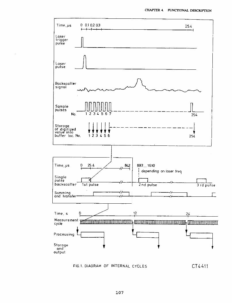
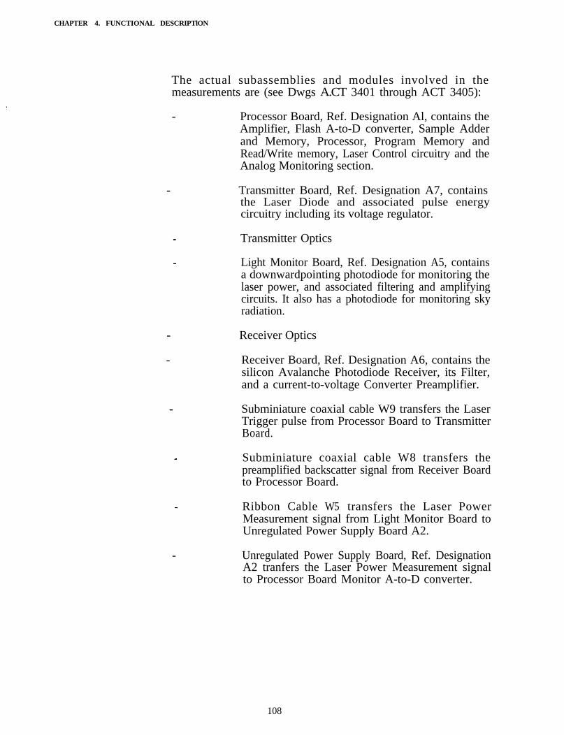
CHAPTER 4. FUNCTIONAL DESCRIPTlON
The actual subassemblies and modules involved in themeasurements are (see Dwgs A.CT 3401 through ACT 3405):
- Processor Board, Ref. Designation Al, contains theAmplifier, Flash A-to-D converter, Sample Adderand Memory, Processor, Program Memory andRead/Write memory, Laser Control circuitry and theAnalog Monitoring section.
- Transmitter Board, Ref. Designation A7, containsthe Laser Diode and associated pulse energycircuitry including its voltage regulator.
Transmitter Optics
Light Monitor Board, Ref. Designation A5, containsa downwardpointing photodiode for monitoring thelaser power, and associated filtering and amplifyingcircuits. It also has a photodiode for monitoring skyradiation.
- Receiver Optics
- Receiver Board, Ref. Designation A6, contains thesilicon Avalanche Photodiode Receiver, its Filter,and a current-to-voltage Converter Preamplifier.
- Subminiature coaxial cable W9 transfers the LaserTrigger pulse from Processor Board to TransmitterBoard.
Subminiature coaxial cable W8 transfers thepreamplified backscatter signal from Receiver Boardto Processor Board.
Ribbon Cable W5 transfers the Laser PowerMeasurement signal from Light Monitor Board toUnregulated Power Supply Board A2.
- Unregulated Power Supply Board, Ref. DesignationA2 tranfers the Laser Power Measurement signalto Processor Board Monitor A-to-D converter.
108
4.2.2.2 The Output Interfaces
CHAPTER 4. FUNCTIONAL DESCRIPTION
The Output Interfaces of the Ceilometer are (Ref. Block DiagramCT 2295):
RS-232C Interface: RS-232C interface of CTS 12 (A2)is mainly for maintenance andservice purposes; routed to theEquipment base connector J4 withinternal cablings.
FSK Bell 103 Interface: Standard modem interface isprovided by CTI 12; (A3), one linepair routed with internal cablingsto the Equipment base connectorJ3.
Gifft RBC Recorder Output: Interface for Gifft RBC Recorderis provided by CTI 12; (A3) two linepairs routed with internal cablfngsto the Equipment base connectorJ3.
The FSK and RS-232C interfaces are internally combined into oneserial two-way processor interface, so that outputs from theCeilometer are identical at both interfaces. Inputs from the twointerfaces are “OR’ed” so that any one may serve as input.Simultaneous inputs are forbidden; the latter lead to erroneousinput characters.
The RxD and TxD signals are connected at the 5V level to themicroprocessor internal Universal Asynchronous ReceiverTransmitter (UART). This is operated by software. Its Baud rateis determined by software through one of the microprocessor’sinternal counters. The Baud rate of the RS-232C interface of theCTS 12 board is 300 Baud as standard and default, but may becommanded to operate at 1,200 Baud.
The RS-232C interface is normally connected to the processor butmay be manually switched to the FSK modem equipment side forFSK line troubleshooting purposes.
Beside RxD, TxD, and Grrd signals, the RS-232C connection ofUnregulated Power Supply board A2 also contains a + 12V DCpower supply and a Flag signal. These are used for theCeilometer Maintenance Terminal CTH 12. This is powered fromthe Ceilometer, and since its keyboard is 16-key hexadecimal, theFlag is needed to signal the processor to interpret inputs from theterminal according to its special protocol.
109
CHAPTER 4. FUNCTIONAL DESCRIPTION
CTH 12 Maintenance Terminal interfaces directly to theEquipment Base connector J4 to where Unregulated Power SupplyRS-232C interface of Board A2 is routed by internal cablings.
Internally, the RS-232C interface of Board A2 is connected viaa standard male 25-pin D-subminiature connector, which thusenables connections with standard cables for in-depth maintenanceand service operations.
The standard asynchronous character frame is:
1 start bit
8 data bits (whereof: 7 used for std USASCII 1 “MSB” isnormally TRUE but used for 8-bit specialcharacters, when initiating the display ofthe Maintenance Terminal)
No Parity
1 Stop bit
Total character count is 10.
Due to the last data bit being TRUE in std ASCIIcommunication, the character appears to have two stop bits.
The FSK Interface is Bell 103-compatible; transformer coupledand balanced. It is based on a monolithic single-chip modem witha jumper to operate either in Originate or Answer mode; thelatter is standard. Its transmission rate is a fixed 300 Baud. Theoutput signal level can be set with a jumper to five differentlevels.
110
CHAPTER 4. FUNCTIONAL DESCRIPTION
Outputs for the Gifft RBC Recorder are:
1 Trigger break, which initiates the recorder sweep.
1 Inscription signal, which (when active) makes a mark on therecorder chart.
These outputs are controlled by the processor and its software viatwo output ports. The signals are routed via the UnregulatedPower Supply board A2 to the Output Interface board A3 wherethe Trigger Break operates a normally closed relay contact andthe Inscription Signal connects a 120 Hz signal, derived from theline frequency 60 Hz by full wave rectification via an isolationtransformer, to the output line.
The inscription signal resolution is 20 ms corresponding to 80 ft;the full sweep is 3 s corresponding to 12,000 ft. The inscriptionsignal timing starts at the end of the trigger break signal.
Refer to Drawing 4412.
If faults are detected, they are signalled by activating the triggerbreak for 200 ms, which causes the “projector” lamp on the GifftRBC Recorder to blink.
111
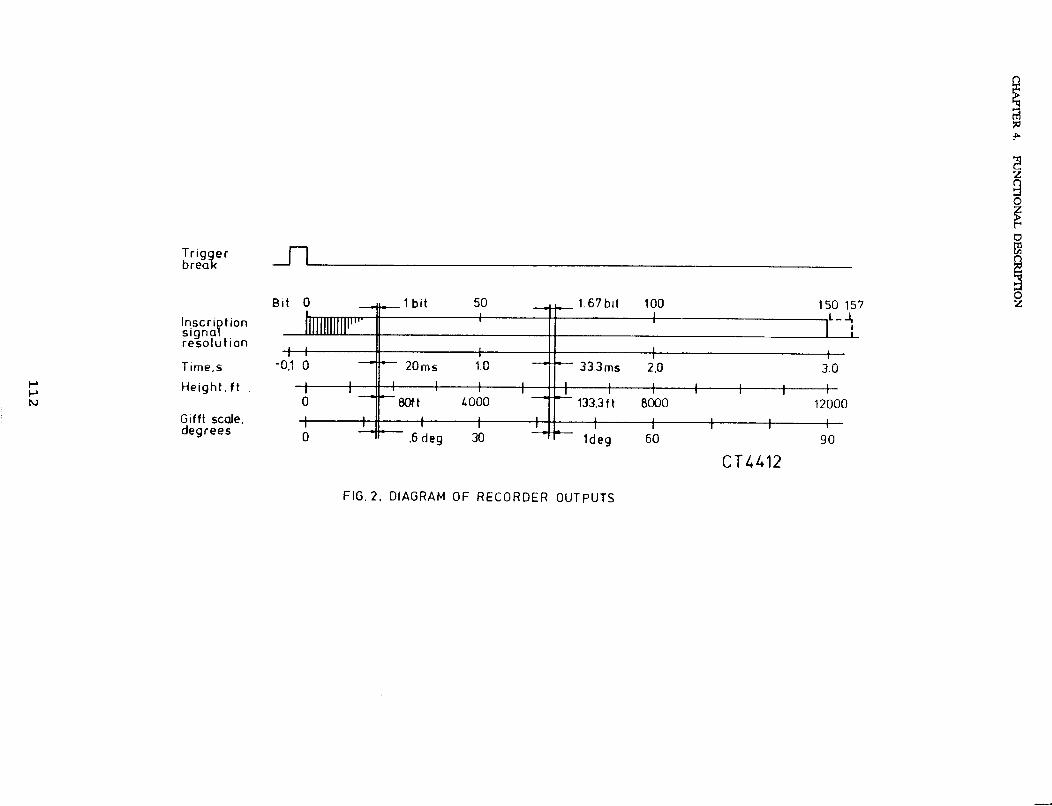
CHAPTER 4. FUNCTIONAL DESCRIPTION
4.2.2.3
The FSK and Recorder outputs are connected by Output HarnessW3 to Output Interface Connector J3 at the Equipment Base.Primary surge protectors in the form of noble gas filled sparkgaps are placed at the J3 connector. Secondary surge protectorsin the form of series resistors and transient zener diodes areplaced on the Output Interface Board.
The internal RS-232C interface is connected via male 25-pin D-subminiature connector J7 on the Unregulated Power SupplyBoard A2 with Maintenance Terminal Harness W4 toMaintenance Terminal Connector J4 at the Equipment Base. Thesignals are protected by series resistors and transient zeners.
Internal Temperature Control
Internal temperature is controlled by switching the twoTemperature Control Heater resistors Rl and R2 “OFF,” in“series” or in “parallel.” The controller is situated on theprocessor board Al and uses a monolithic l0mV/°K temperaturesensor. This is connected to two voltage comparators, which havereference set points at about 0°C (32°F) and 20°C (68°F). Thecomparators drive relays Kl and K2 on the Unregulated PowerSupply Board A2 which connect power from Temperature ControlTransformer Tl to Rl and R2. The processor has no controlover the heating, but does monitor the temperature.
In indoor conditions and warmer, both relays are “OFF” and noheating power is connected.
Between 0°C (32°F) and 20°C (68°F) relay Kl is ON connectingthe resistors to the transformer in series. Heating power will beapproximately 20 W.
Below 0°C relay K2 in ON and relay Kl is forced OFF,connecting Rl, R2 in parallel to Tl. Heating power will beapproximately 80 W.
Without heating, internal temperature will be 5°C...l0°C(l0°F...20°F) above ambient, after stabilizing.
With full heating, internal temperature will be 20°C...30°C(40°F...60°F) above ambient, after stabilizing.
The time constant of the internal temperature is about 2 hoursin calm conditions.
113
CHAPTER 4. FUNCTIONAL DESCRIPTION
4.2.2.4
4.2.2.5
4.2.2.6
Internal Monitoring
The hardware for the internal monitoring consists mainly of theScaling network, Selector and Monitor A-to-D Converter of theProcessor Board Al. The actual alarm limits and algorithms areimplemented in software, which also monitors and checks otherfunctions.
The summary of the use of the Monitor A-to-D channels ispresented in the Appendix of Chapter 3.
Power Supply Section
This consists of the High Voltge Power Supply PSl, theUnregulated Power Supply Board A2, and the TemperatureControl Transformer Tl.
This section supplies unregulated power to all subassemblies,where the actual voltage regulators are located.
Solar Shutter Option
The option must be furnished if the geographical location is suchthat the sun may be right above the instrument (i.e., between thetropics of Capricorn and Cancer, plus some safety margin).
The solar shutter Kl consists of a solenoid and a flap placedabove the transmitter lens. The receiver is adequately protectedby its filter.
The sunlight sensor and solar shutter driver electronics aresituated on the Light Monitor Board A5.
The shutter design is fail-safe (i.e., when no power is applied itis closed). The solenoid has to be energized to open. This isdone by the electronics circuits without the need of processorcontrol.
The processor is able to read the Sky Light sensor. Theprocessor can also drive the shutter “ON” for testing purposes, butcannot force it to be “OFF’ when the shutter circuit detectsexcessive light.
Note that in all documentation, Shutter “ON” corresponds tosolenoid current being “OFF” and vice versa, due to the fail-safedesign.
114
CHAPTER 4. FUNCTIONAL DESCRIPTION
4.2.2.7 Window Conditioner
The Window Conditioner is controlled by two outputs from theProcessor Board. These are routed through the UnregulatedPower Supply Board A2 connector Jll to High Voltage PowerSupply PSl to drive two relays. These switch Line Power to theblower and the heater of the Window Conditioner via connectorJ2. The relays are connected so that the heater can never getpower without the blower being on.
Window Conditioner line power has its own circuit breaker CB2in PS1.
The Window Conditioner is monitored with a temperature sensor,software reference TB, which is placed in the warm air stream.This senses both the effect of the heater, and a potential blowermotor failure that would cause a rapid increase in TB (when theheater is “ON”). For safety reasons, the heater also has athermostat which breaks its current at about 250°F (120°C).
115

116
Archive
CHAPTER 4. FUNCTIONAL DESCRIPTION
Archive
Archive
120
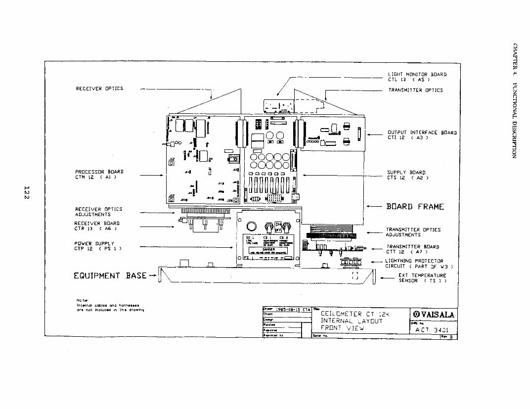
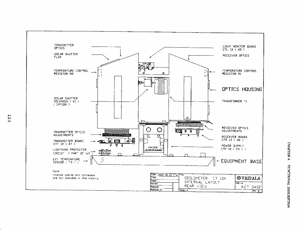
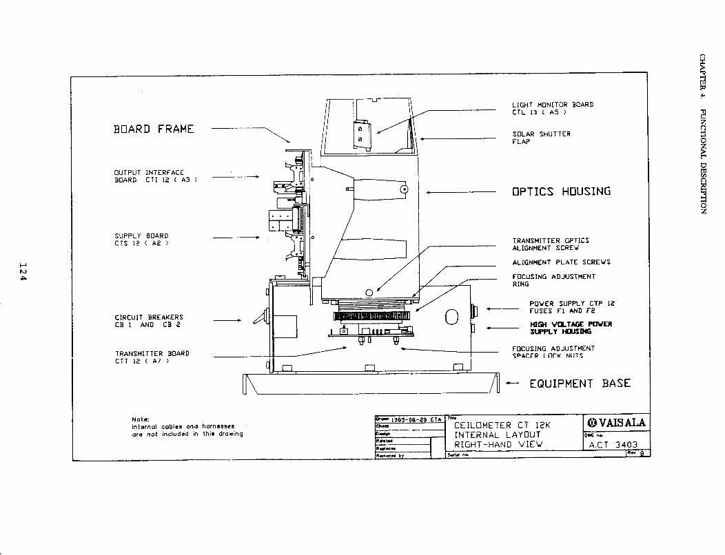
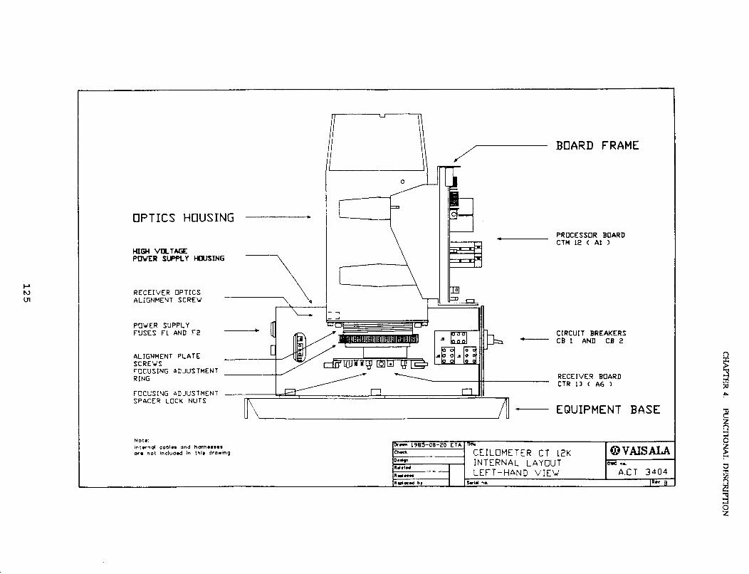
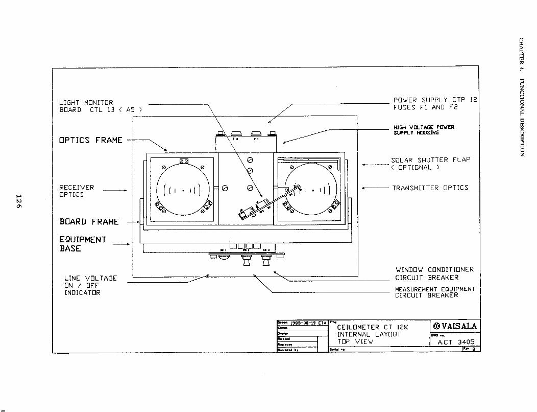
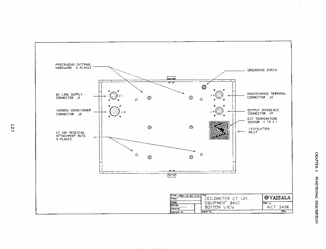
CHAPTER 4. FUNCTIONAL DESCRIPTION
4.3 MODULE DESCRIPTIONS
4.3.1 PROCESSOR BOARD Cl-M 12 REF. Al
4.3.1.1 General
The CTM 12 is the main signal conditioning and processing unitfor the CT 12K Ceilometer. On a single size PC board itcontains all the electronics to:
control laser pulse triggering at software determined intervals.
buffer and amplify by software controlled gain thebackscattered echo signal from the Receiver Board.
sample, convert, and store the amplified echo signal.
digitally integrate the stored series of samples throughout thedetecting range.
process the echo signal data and calculate the cloud baselevels and other relevant data according to software rules.
transfer data and commands through the on-board serialRS-232C port.
monitor the unregulated power supply voltages, Transmitterand Receiver operating voltages, laser power, ambient lightlevel, and temperatures measured at four points of the system.
control the Window Conditioner and optional Solar Shutteraccording to monitored parameter values and software rules.
automatically control internal heating of the Ceilometer.
The Principal Data and Control Flow of the CTM 12 is illustratedin Drawing CT 4532 and further described below:
128
CHAPTER 4. FUNCTIONAL DESCRIPTION
Main data processing in the unit is carried out by an 8031-typeof microprocessor and its related hardware: 64 k byte EPROMfor instruction memory and 8 k byte RAM for data memory.Furthermore the on-board EEPROM provides for 1 k bitnonvolatile storage for scaling factors and other importantparameters. Through its integral UAR/T and two integral timers,the processor maintains serial asynchronous communication andtime-keeping in the system. A watch-dog timer provides forforced resetting of the processor in case of temporary malfunction.
The echo signal from the Receiver Board is first amplified andthen converted into a digital form by a 6 bit Flash ADC takingone sample every 100 ns. This corresponds to 50 ft (15m) stepsin backscattered laser light pulse path. These 254 convertedsamples are stored into the fast RAM and then added byhardware to the respective sum of previously taken samples. Thecumulated samples sums, which form the integrated results foreach 50 ft range gate, are then stored into the fast RAM.
Monitoring the power supply voltages and other relevant systemparameters is carried out by a specific 19-channel ADC circuitrywhich features S-bit conversion resolution and a bit-by-bit serialinterface for interchanging channel addresses and conversionresults with the processor.
The operating voltages of the CTM 12 are all supplied byon-board voltage regulators, some of which also feed the OutputInterface Board CTI 12, Ref. A3. Several on-board precisionreference supplies for measurement needs are also provided.
The board was designed and realized to be easily maintainable.Seventy-eight (78) test points provide for easy access to the mostimportant signals. Jumper strappings on selected feed-back signalpaths facilitate testing on component level. The board includesa test pulse generator, from which several different echo signalcombinations are attainable for simulating cloud base conditionswithout the need of an optical path. Parameter monitoringcapability further provides for easy isolation of failures both oncomponent and board level.
The CTM 12 Processor Board was specified and designed for lowpower operation in a wide temperature range. The total powerconsumption of the board is typically 6 Watts, about 40% ofwhich is dissipated by the on-board voltage regulators.
129
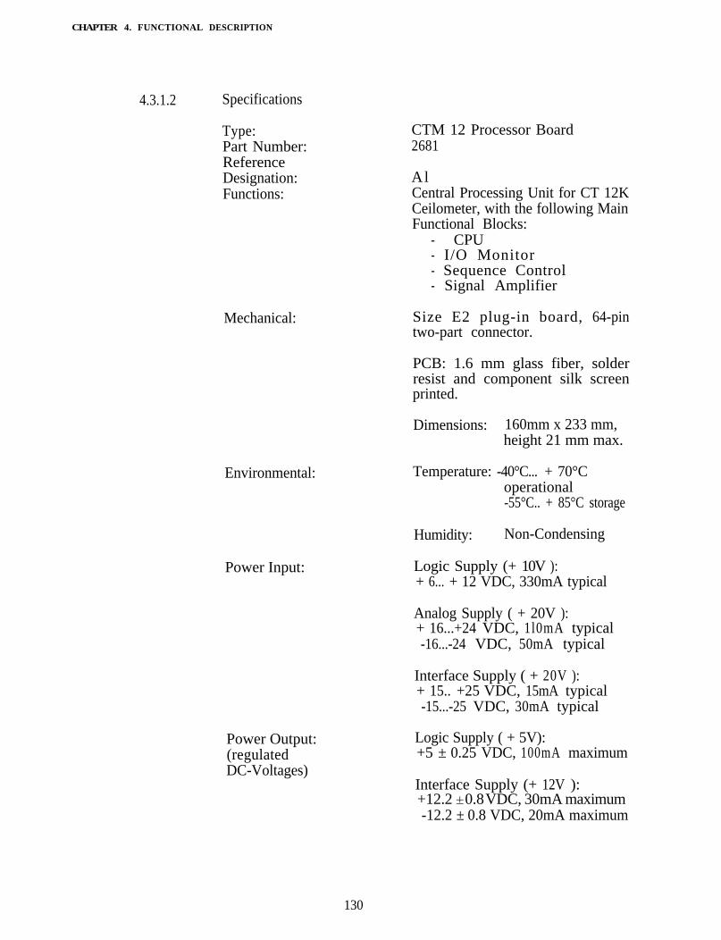
CHAPTER 4. FUNCTIONAL DESCRIPTION
4.3.1.2 Specifications
Type:Part Number:ReferenceDesignation:Functions:
Mechanical:
Environmental:
Power Input:
Power Output:(regulatedDC-Voltages)
CTM 12 Processor Board2681
AlCentral Processing Unit for CT 12KCeilometer, with the following MainFunctional Blocks:
- CPU- I/O Monitor- Sequence Control- Signal Amplifier
Size E2 plug-in board, 64-pintwo-part connector.
PCB: 1.6 mm glass fiber, solderresist and component silk screenprinted.
Dimensions: 160mm x 233 mm,height 21 mm max.
Temperature: -40°C... + 70°Coperational-55°C.. + 85°C storage
Humidity: Non-Condensing
Logic Supply (+ 10V ):+ 6... + 12 VDC, 330mA typical
Analog Supply ( + 20V ):+ 16...+24 VDC, 1l0mA typical-16...-24 VDC, 50mA typical
Interface Supply ( + 20V ):+ 15.. +25 VDC, 15mA typical-15...-25 VDC, 30mA typical
Logic Supply ( + 5V):+5 ± 0.25 VDC, 100mA maximum
Interface Supply (+ 12V ):+12.2 ± 0.8 VDC, 30mA maximum-12.2 ± 0.8 VDC, 20mA maximum
130
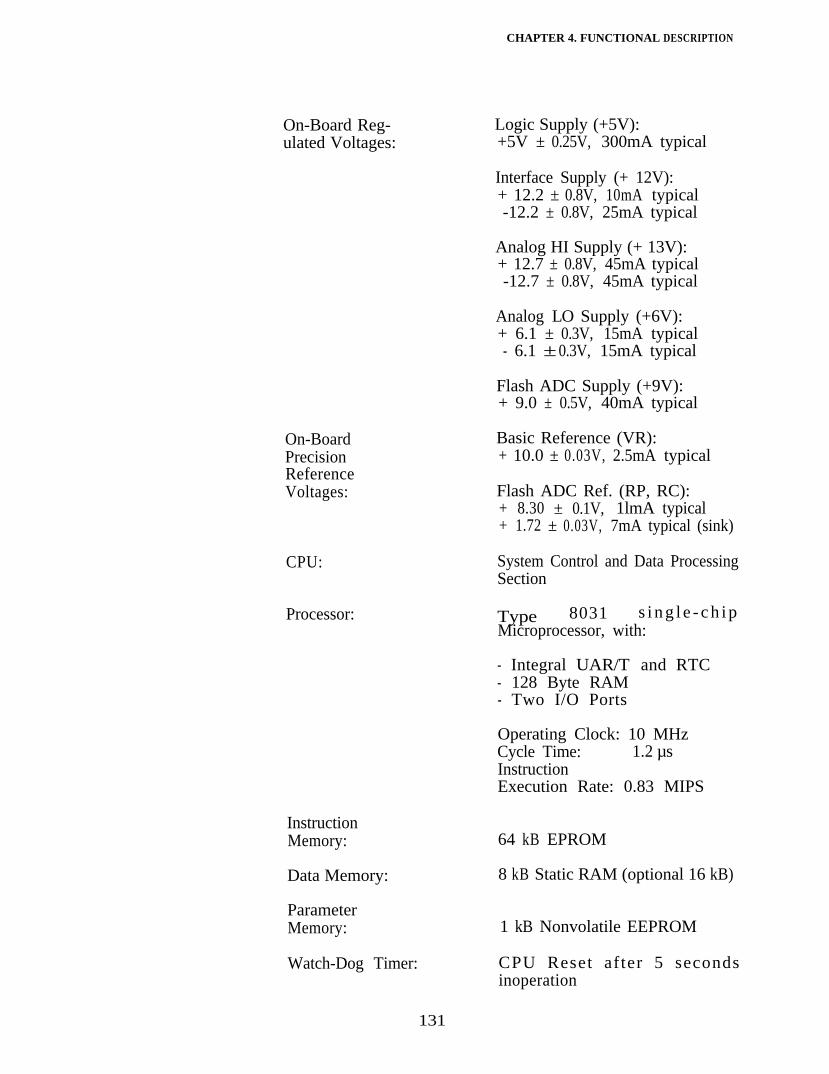
CHAPTER 4. FUNCTIONAL DESCRIPTION
On-Board Reg- Logic Supply (+5V):ulated Voltages: +5V ± 0.25V, 300mA typical
On-BoardPrecisionReferenceVoltages:
CPU:
Processor:
Interface Supply (+ 12V):+ 12.2 ± 0.8V, 10mA typical-12.2 ± 0.8V, 25mA typical
Analog HI Supply (+ 13V):+ 12.7 ± 0.8V, 45mA typical-12.7 ± 0.8V, 45mA typical
Analog LO Supply (+6V):+ 6.1 ± 0.3V, 15mA typical- 6.1 ± 0.3V, 15mA typical
Flash ADC Supply (+9V):+ 9.0 ± 0.5V, 40mA typical
Basic Reference (VR):+ 10.0 ± 0.03V, 2.5mA typical
Flash ADC Ref. (RP, RC):+ 8.30 ± 0.1V, 1lmA typical+ 1.72 ± 0.03V, 7mA typical (sink)
System Control and Data ProcessingSection
Type 8031 s i n g l e - c h i pMicroprocessor, with:
- Integral UAR/T and RTC- 128 Byte RAM- Two I/O Ports
Operating Clock: 10 MHzCycle Time: 1.2 µsInstructionExecution Rate: 0.83 MIPS
InstructionMemory:
Data Memory:
64 kB EPROM
8 kB Static RAM (optional 16 kB)
ParameterMemory: 1 kB Nonvolatile EEPROM
Watch-Dog Timer: CPU Reset after 5 secondsinoperation
131
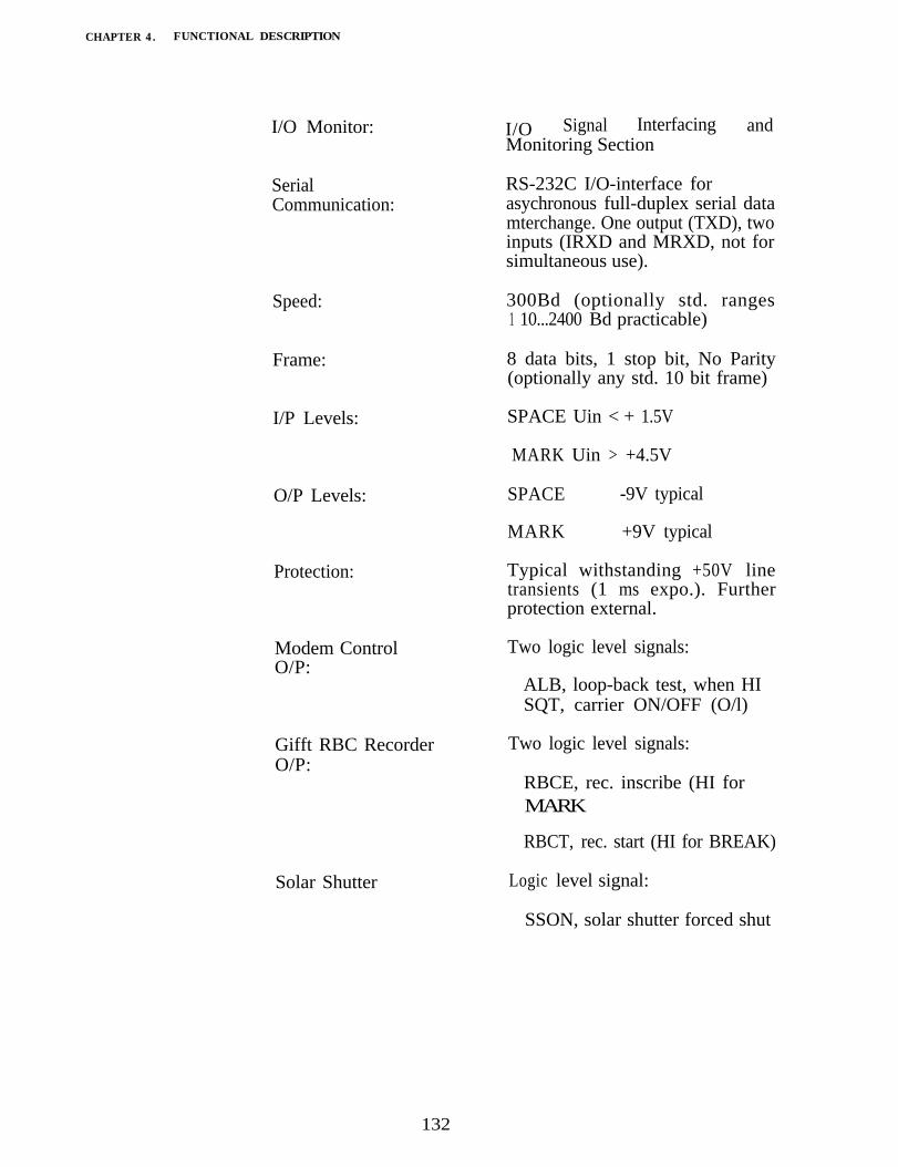
CHAPTER 4. FUNCTIONAL DESCRIPTION
I/O Monitor:
SerialCommunication:
Speed:
Frame:
I/P Levels:
O/P Levels:
Protection:
Modem ControlO/P:
I/O Signal Interfacing andMonitoring Section
RS-232C I/O-interface forasychronous full-duplex serial datamterchange. One output (TXD), twoinputs (IRXD and MRXD, not forsimultaneous use).
300Bd (optionally std. ranges1 10...2400 Bd practicable)
8 data bits, 1 stop bit, No Parity(optionally any std. 10 bit frame)
SPACE Uin < + 1.5V
MARK Uin > +4.5V
SPACE -9V typical
MARK +9V typical
Typical withstanding +50V linetransients (1 ms expo.). Furtherprotection external.
Two logic level signals:
ALB, loop-back test, when HISQT, carrier ON/OFF (O/l)
Gifft RBC RecorderO/P:
Two logic level signals:
RBCE, rec. inscribe (HI forMARK
RBCT, rec. start (HI for BREAK)
Solar Shutter Logic level signal:
SSON, solar shutter forced shut
132
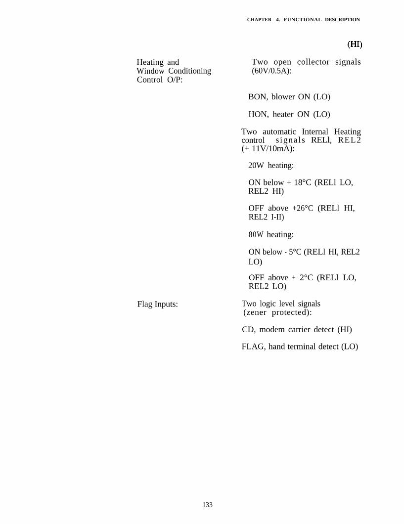
CHAPTER 4. FUNCTIONAL DESCRIPTION
Heating andWindow ConditioningControl O/P:
Two open collector signals(60V/0.5A):
BON, blower ON (LO)
HON, heater ON (LO)
Two automatic Internal Heatingcontrol s ignals RELl, REL2(+ 11V/10mA):
20W heating:
ON below + 18°C (RELl LO,REL2 HI)
OFF above +26°C (RELl HI,REL2 I-II)
80W heating:
ON below - 5°C (RELl HI, REL2LO)
OFF above + 2°C (RELl LO,REL2 LO)
Flag Inputs: Two logic level signals(zener protected):
CD, modem carrier detect (HI)
FLAG, hand terminal detect (LO)
133
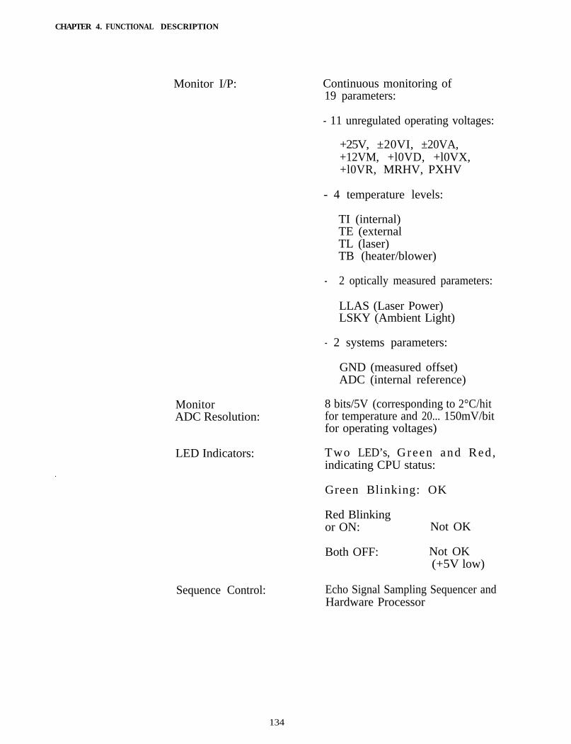
CHAPTER 4. FUNCTIONAL DESCRIPTION
Monitor I/P: Continuous monitoring of19 parameters:
- 11 unregulated operating voltages:
+25V, ±20VI, ±20VA,+12VM, +l0VD, +l0VX,+l0VR, MRHV, PXHV
- 4 temperature levels:
TI (internal)TE (externalTL (laser)TB (heater/blower)
- 2 optically measured parameters:
LLAS (Laser Power)LSKY (Ambient Light)
- 2 systems parameters:
GND (measured offset)ADC (internal reference)
MonitorADC Resolution:
8 bits/5V (corresponding to 2°C/hitfor temperature and 20... 150mV/bitfor operating voltages)
LED Indicators: Two LED’s, Green and Red ,indicating CPU status:
Green Blinking: OK
Red Blinkingor ON: Not OK
Both OFF: Not OK(+5V low)
Sequence Control: Echo Signal Sampling Sequencer andHardware Processor
134
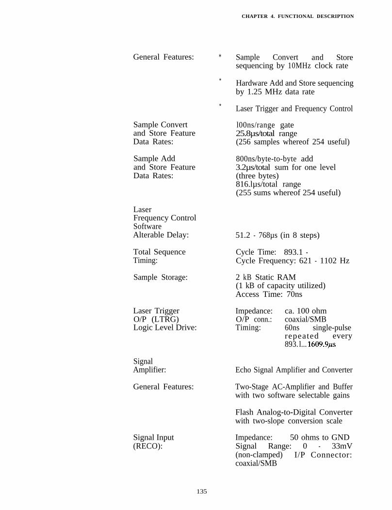
CHAPTER 4. FUNCTIONAL DESCRIPTION
General Features: * Sample Convert and Storesequencing by 10MHz clock rate
* Hardware Add and Store sequencingby 1.25 MHz data rate
* Laser Trigger and Frequency Control
Sample Convert l00ns/range gateand Store Feature 25.8µs/total rangeData Rates: (256 samples whereof 254 useful)
Sample Addand Store FeatureData Rates:
800ns/byte-to-byte add3.2µs/total sum for one level(three bytes)816.lµs/total range(255 sums whereof 254 useful)
LaserFrequency ControlSoftwareAlterable Delay:
Total SequenceTiming:
Sample Storage:
Laser TriggerO/P (LTRG)Logic Level Drive:
SignalAmplifier:
General Features:
Signal Input(RECO):
135
51.2 - 768µs (in 8 steps)
Cycle Time: 893.1 - 1609.9µsCycle Frequency: 621 - 1102 Hz
2 kB Static RAM(1 kB of capacity utilized)Access Time: 70ns
Impedance: ca. 100 ohmO/P conn.: coaxial/SMBTiming: 60ns single-pulse
repeated every893. l... 1609.9s
Echo Signal Amplifier and Converter
Two-Stage AC-Amplifier and Bufferwith two software selectable gains
Flash Analog-to-Digital Converterwith two-slope conversion scale
Impedance: 50 ohms to GNDSignal Range: 0 - 33mV(non-clamped) I/P Connector:coaxial/SMB
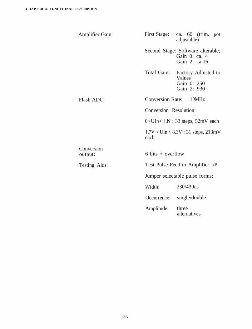
CHAPTER 4. FUNCTIONAL DESCRIPTION
Amplifier Gain:
Flash ADC:
Conversionoutput:
Testing Aids:
First Stage: ca. 60 (trim. potadjustable)
Second Stage: Software alterable;Gain 0: ca. 4Gain 2: ca.16
Total Gain: Factory Adjusted toValuesGain 0: 250Gain 2: 930
Conversion Rate: 10MHz
Conversion Resolution:
0<Uin< l.N : 33 steps, 52mV each
1.7V < Uin < 8.3V : 31 steps, 213mVeach
6 bits + overflow
Test Pulse Feed to Amplifier I/P.
Jumper selectable pulse forms:
Width: 230/430ns
Occurrence: single/double
Amplitude: threealternatives
136
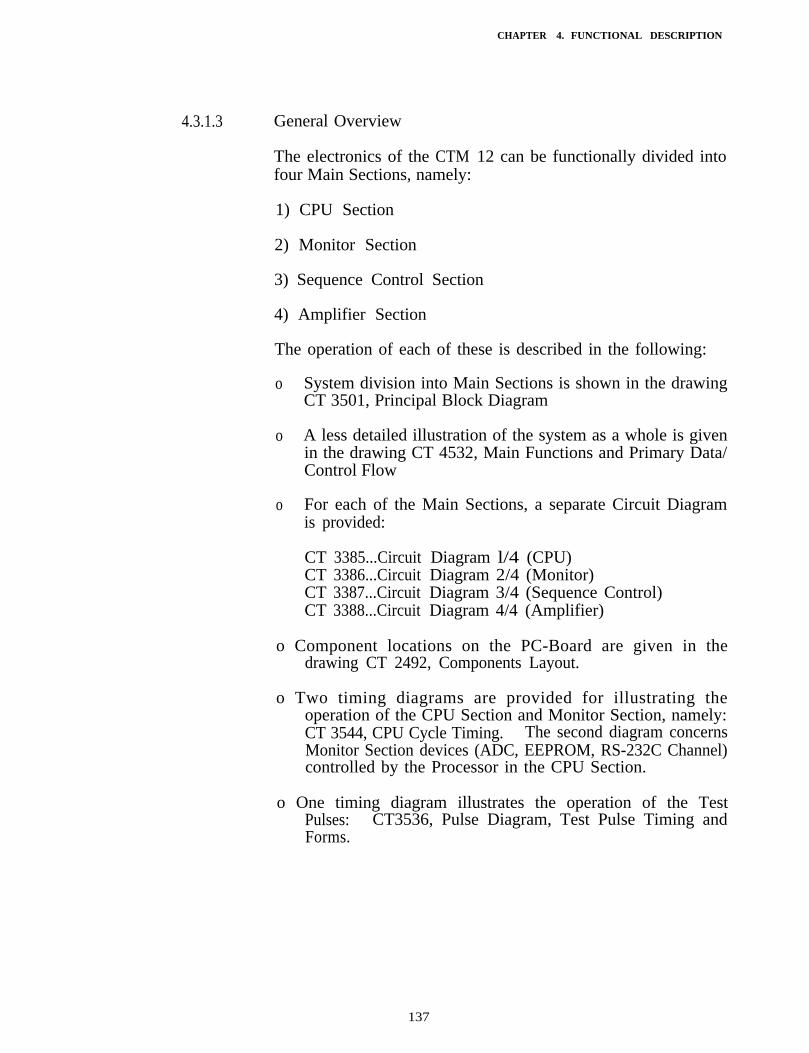
CHAPTER 4. FUNCTIONAL DESCRIPTION
4.3.1.3 General Overview
The electronics of the CTM 12 can be functionally divided intofour Main Sections, namely:
1) CPU Section
2) Monitor Section
3) Sequence Control Section
4) Amplifier Section
The operation of each of these is described in the following:
o System division into Main Sections is shown in the drawingCT 3501, Principal Block Diagram
o A less detailed illustration of the system as a whole is givenin the drawing CT 4532, Main Functions and Primary Data/Control Flow
o For each of the Main Sections, a separate Circuit Diagramis provided:
CT 3385...Circuit Diagram l/4 (CPU)CT 3386...Circuit Diagram 2/4 (Monitor)CT 3387...Circuit Diagram 3/4 (Sequence Control)CT 3388...Circuit Diagram 4/4 (Amplifier)
o Component locations on the PC-Board are given in thedrawing CT 2492, Components Layout.
o Two timing diagrams are provided for illustrating theoperation of the CPU Section and Monitor Section, namely:CT 3544, CPU Cycle Timing. The second diagram concernsMonitor Section devices (ADC, EEPROM, RS-232C Channel)controlled by the Processor in the CPU Section.
o One timing diagram illustrates the operation of the TestPulses: CT3536, Pulse Diagram, Test Pulse Timing andForms.
137
CHAPTER 4. FUNCTIONAL DESCRIPTION
4.3.1.4 Functional Description
4.3.1.4.1 CPU Section:
The Microprocessor U4 is an 8031-type single-chip NMOS-devicemounted on a socket. Beside the typical processing elements, itcontains:
128 bytes of data memory, in this application most is used forthe stack and general purpose registers
two 16-bit timers, one of them is used as a Baud rate clock,the other is used as a Real Time Clock (RTC)
integral Universal Asynchronous Receiver/Transmitter(UAR/T)
two general purpose I/O ports, Pl and P3
For instruction set and other details, see REFERENCE.
The Processor’s AD-bus is pulled high by resistors in the arrayRA8. This is to better meet the input level demands of the stan-dard CMOS devices on the bus. It also enables testing of theboard with the EPROM removed. In that case, the Processorrepeatedly fetches the code FFH from the bus, which correspondsto a nonbranch internal operation instruction. Thereby, theProcessor keeps running with its address outputs incrementingthrough the address space, which is a convenient condition forisolating failures on the bus.
The Address Latch U13 is a transparent type of latch. WhenALE (pin 11) is high, its input states show in the output. WhenALE goes low, the current output states (address) are latched.
The Instruction Memorv U3 is a 64-k byte CMOS-EPROM, type27C512 (mounted on socket). The EPROM is continuouslyactivated with its chip select pin 20 grounded. Its output buffersare enabled, when pin 22 is driven low by PSEN.
It should be noted that the E P R O M is erased by UV-light, andthus the label on its window should not be removed. EPROMwith no shield on its window will be erased in approximately oneweek when exposed to direct sunlight.
138
CHAPTER 4 . FUNCTIONAL DESCRIPTION
The Data Memorv U2 is an 8 k byte static CMOS-RAM device,type TC 5564 or equivalent (mounted on socket). Its chip selectpin 20 is driven by A14, activating the device only when the RAMarea of the I/O address space is addressed. Its output buffersare enabled with pin 22 driven low by RRO. Writing is carriedout by driving pin 27 low by RWO. Provisions have been madeon the board (Ul) for another similar or 2 kB device.
The RD/WR Decoder U 9 is a double 2-to-4 line decoder device.Low state on its pin 15 activates one of its Read strobe outputs.Low state on its pin 1 activates one of its Write strobe outputs.
The Watch-Dog; Timer consists of the 14-bit ripple counter U12clocked by the RC-oscillator: U11/8, RA7/5-6, C15. Counterreset (pin 12) is activated via Ul l/2-3 by WDR generated bysoftware. If not reset, the counter will count up until after 8192clock pulses (ca. 5 seconds), and it raises PRES high via diodeDA2/15-2, thus resetting the processor. For testing purposes,Jumper J8 can be removed thus eliminating the Watch-Dog.
The Reset circuitry consists of the three Schmitt-trigger gates ofU20 and some passive components. During the PWR-ONtransition POR is low driving U20/3 high, thus resetting theProcessor via diode DA2/14-3. U20/11 produces System Reset(RS low). Via Ull/l-3 also, the Watch-Dog counter is reset.The capacitance Cl6 is discharged through the 22 k resistor inthe POR line (Monitor Section) and will hold the Resetapproximately 400 ms after PWR-ON. Reset can also beactivated manually by actuating the momentary switch Sl(upwards) and so grounding the POR line via the resistors inRA7.
The Sample Data Latch U19 is a similar transparent type ofdevice as U13. In the initial state, RL is high thus making thelatch transparent via its pin 11. On the other hand, it disablesthe latch output buffers via pin 1. When reading the sampleRAM, RL is strobed low, which makes U19 latch the data on theSD-bus and output them into the AD-bus to be loaded in by theProcessor. Latching is used because the data on the SD-buschanges invalid soon after the falling edge of RL.
System Clock for the Monitor ADC is provided by theRC-oscillator: Ul l/6, RA7/7-8, C9. Two Schmitt-trigger gates,Ull/ll and U20/6, are unused and their inputs are tied to stablelevels.
RS-232C signals IRXD and MRXD are OR’ed by diodes in DA2and filtered by RA7/7-8 and C18. U20/8 inverts the results andalso provides level clamp by its integral input protecting diodes,which limit the signal level between +5 V and GND.
139
CHAPTER 4. FUNCTIONAL DESCRIPTION
Input Signals FLAG and CD coming from the outside of theboard are transient protected by resistors in RAl and 5.1 V zenerdiodes Dl and D3.
Test points are provided for the following signals:
J3/10-3: AO-7, Address LO byteJ7/ 10-3: ADO-7, AD-busJ5/3: X2, CPU clockJ5/4: PRES, CPU resetJ5/5: TXD, Serial Line Xmitted DataJ5/6: RXD, Serial Line Received DataJ5/7: ALE, Address Latch EnableJ 5 / 8 : PSEN, Program Store EnableJ6/3: RS, System ResetJ6/4: WR, I/O Write StrobeJ6/5: RD, I/O Read StrobeJ6/8: +5 V, Logic SupplyJ6/9: RL, Sample Latch EnableJ3,J5,J6,and J7/1: GND, Logic Ground
4.3.1.4.2 Monitor Section
The Monitored Signals are brought into the board via the edgeconnector Jl. The resistor arrays RA3, RA4, RA5, RAll (9x2k2,4x4k7, 4x4k7, 4xl0k), and resistor R5 (14k7) perform scaling ofthe signals. The signals LLAS, LSKY, PXHV and MRHV arenot attenuated but carried through series resistors. LLAS andLSKY lines are protected by diodes (DAl) clamping to +5 V,as they originate in the A5 op amps, powered from + 17 V (Ref.A5).
Negative bias for the Temperature Sensors is applied through 2k2resistors (RA13) to the TL-, TE-, and TB-lines on Jl. The biassupply is regulated by D2, 5.1 V zener diode, giving but outputof only -4.8 V due to restricted zener current. The negative levelsignals from the Temperature Sensors (TL+, TE+ , TB + ) arebrought in through 4k7 resistors.
The positive level signals connect to channel input pins l-9, 11of the Monitor ADC U8. The negative level signals connect toU15, the Pre-MUX. This also includes the on-board TemperatureSensor (U16) output carried through the resistor RA12/5- 6. Thechannel i/p, full scale level and conversion resolution for all theMonitor inputs are defined in Table 3.
140
CH APTER 4. FUNCTIONAL DESCRIPTION
The Pre-Multiplexer U15 is a type 4051 CMOS analog MUX. Itis an 8-channel device capable of switching also negative signallevels, provided that negative bias is applied to its pin 7.Multiplex address is applied to pins 11-9 (P14-16). Multiplexoutput from pin 3 is filtered by RA2/6-5 and C13, and thenbuffered by U14/7 op-amp prior to feeding it into the AmplifierSection (MB) where it is inverted and brought back (MI) to theMon. ADC pin 12 (CH 10).
The monitor ADC U8 is a CMOS-device of type TLC 541. Itconverts one-by-one the signals applied to its 11 channel inputsinto digital 8-bit form. The twelfth channel, internal self-testvoltage brings out about a half of the full-scale reading (12823).The ADC control section provides for serial address/datainterchange with the host. The I/O clock (18) carries outclocking in the channel address (17) and clocking out conversiondata (16). Pin 15 is the low-active chip select input. The ADCreference voltage V5, which originates in the Amplifier Section,is applied to pin 14. As supplied by an op amp powered from+ 13 V, the line is protected by the DA1 diodes. This appliesalso to the signal input MI.
ConversionSignal Jl ADC MUX FS Level ResolutionID pin(s) Channel Channel on Jl per bit
P201 ac2P20A a c 3 0P25V acllPl0D a c 2 7Pl0R c9Pl0X a9P12M c8PXHV a8L L A S c6LSKY a6MTE c l 4MTB c l 5MTI -MTL cl3M201 a c 3MRHV acl0M20A acl0G N D ( - )INT SELF TEST 11
0123
56789
1010101010101010
x 1) -
+27.7 V 108 mV+27.7 V 108 mV+38.4 v 150 mV+ 15.6 V 61 mV+ 15.6 V 61 mV+ 15.6 V 61 mV+ 15.6 V 63 mV+ 5.0 v 20 mV 4)
+ 5.0 v 20 mV+ 5.0 v 20 mV- 4.8 V 2) 20 mV 3)
- 4.8 V 2) 20 mV 3)
I) 20 mV 3)
- 4.8 V 2) 20 mV 3)
-26.6 V 108 mV- 4.8 V 2) 20 mV 4)
-26.6 V 2) 108 mV1) 20 mV
141
Archive
4
CHAPTER 4. FUNCTIONAL. DESCRIPTION
Table 3. Monitored Signals, with Channel I/P, Full-ScaleLevel and Conversion Resolution Shown
Note 1) On-Board Connected
Note 2) Limited by the Pre-Mux Negative Bias
Note 3) Corresponds to Temperature Resolution 2°C/Bit.Code 149 Decimal Corresponds to +25°C.
Note 4) Corresponds to Resolution of 2 V/Bit for originalhigh-voltages. Notice that if Xmitter or Receivercoaxial cables are disconnected, both HIV and LOVvalues for the respective units are unmeasurableby the Monitor. After reconnecting the Xmittercable, PXHV reading may be invalid for some time.
The EEPROM U5 is a 64x16 bit CMOS device of type NMC9346, mounted on socket. It is an Electrically Erasable andProgrammable Read Only Memory preserving its storage duringpower outages. This provides for handling of the EEPROM U5like the EPROM (e.g., removing it from socket and placing intoanother CTM 12 so as to transfer the system parameters). Readand Write access are carried out serially. Transfer clock isapplied to pin 2 (SK) and code/address/data to pin 3 (DI).Data is brought out to pin 4 (DO). Pin 1 is the active high chipselect input.
The O/P Control Latches U10 and U21 are 8-bit addressableCMOS-latches. Access to the latch registers is carried out bypulling pin 14 (LENO, LENl) low, which accomplishes transferringthe pin 13 input state to the output register determined by theaddress on pins 1 through 3. Returning pin 14 high will latch theoutput.
The Latch 1 output pins 11, 12 are buffered by transistors Ql andQ2 which drive the coils of Heater and Blower Relays in the HIVPWR Supply (Ref. PSl). The HON and BON lines are protectedagainst inductive transients by diodes on the Unregulated PowerSupply Board (Ref. A2). The Latch 0 output pins 11, 12 drivethe Green and Red LED indicators through the RA6 resistors.The LED’s provide for high brightness with only 6mA currentsunk by the Latch outputs.
142
CHAPTER 4. FUNCTIONAL DESCRIPTION
The Internal Heating Control is composed of two op-amps ofU14, resistor arrays RA9, RAl0 (4x47k, 4xl00R), and diodeDA2/9-8, and, furthermore, the resistor dividers R7/R8 andR6/RA12 (l-2) which supply the temperature-controlled voltagesto the inv. inputs of the op-amps (13,2). U14 is a quad op-ampLM 124, also providing for the Pre-MUX and TxD buffers on theboard. The op-amps, capable of sinking 10mA min. provide forthe Heating Relay coil drives RELl and REL2 through 100Rresistors. The other couple of 100R resistors in the HC-line,together with the 47k feedback resistors RA9/ 3-4, l-2) achievetyp. +200 mV hysteresis in the control system. The on-boardTemperature Sensor U16 (LM 335), biased through RA12/3-4,controls the circuitry through its linear temperature-dependentvoltage drop.
The +5 V Regulator U29 is a special PNP-type device, LM 2935,mounted on heat-sink. It features very low voltage drop betweenits input (1) and output (2). Only 5.6 volts is needed at the inputfor maintaining the regulation. The Regulator’s output pin 4produces active-low PWR-ON Reset signal POR fed through 22kresistor RA20/7-8 to the CPU section. Pin 5 is a separate +5V output intended to be used as low current standby supply, notused in this application and therefore pulled up by resistors toavoid oscillation. The unregulated input voltage + 10VD isfiltered by Ll and C26. Bypass capacitors, total number of 18,are connected to the +5 V line. Diode D9 protects againstreverse voltages. The Regulator is capable of producing 750 mAoutput current. Less than half of this is used in the system.
The + 12V Regulator U6 is of adjustable type LM317LZ. Itsoutput voltage is determined by the adjust resistors in thefollowing way:
Uout = (1 + R4/R3) x 1.25 V + R3 x 50µA - 12.2 V
The input and output capacitors C5, C4 do the by-passing, as doesCl7 between the ± supplies. Diode DA1/8-9 protects againstreverse voltages. The Regulator is capable of producing 100 mA,less than one-third of which is used in the system.
The -12 V Regulator U7 is of adjustable type LM337LZ, with thesame characteristics and similar circuit realization as the + 12 VRegulator.
The RS-232C Output TxD is driven by one of U14 op-amps,which inverts and level-scales the TxD signal from the Processor.RAl/l-2 and RA2/1-2 provide for input signal threshold. Theoutput is protected by the series resistor RA14/7-8 and the clampdiodes in DA2.
143
CHAPTER 4. FUNCTIONAL DESCRIPTION
Test Points are provided for the following signals:
J5/10: + 12 V, I/F Positive SupplyJ5/9: -12 V, I/F Negative SupplyJ6/10: Gl, Amplifier Gain ControlJ6/7: V5, Mon. ADC Ref. SupplyJ 6 / 6 : MI, Pre-MUX Inverted O/P
4.3.1.4.3 Sequence Control Section
The Time Base is obtained from the four unbuffered inverters inU33. One of them is the oscillator, controlled by crystal Z1.RA23/7-8 and R34 provide for bias and by-pass, C38 and Xl, X2.U33/4 outputs the Seq. Control Clock Xl applied to U38/9 andU43/13 in Freq. Divider and Control block.
The Frea. Divider and Control is composed of the JK-Flip-Flopin U43 and the NOR-gates U38/8 and 6. The clock Xl is fedeither through the F-F, its frequency divided by two (LTE) SQOapplied to U38/10, 11 and the J-input of U43. SQO low or highresults in 10 MHz or 5 MHz on U38/6, respectively. ST lowapplied to the set input of U43 entirely inhibits the clockfeed-through and sets U38/6 low.
The Write Pulse Shaper is formed by the NAND-gate U52/6 andthe delay generating circuits U38/6 and U45/2 (its inputcapacitance driven through paralleled resistors). During SQPHO,the NAND-gate outputs a 10 MHz pulse freq. with ca. l/3 dutycycle, suitable for Write accessing the Sample RAM.
The Sea. Control Counter consists of the three similar 4-bitsynchronous counter circuits U42, U37, and U32 which featuresynchronous operation. Load Control (pin9) is used in two of thecounters: in U42, to inhibit the first counter stage by loading inall-ones; and, in U32, for loading in Pll through 13 to the thirdcounter stage. RS applied to pin 1 resets the counters atPWR-ON or Manual Reset.
The Sea. Control Register consists of the JK-Flip-Flops of U51,and the AND-gates of U50, and the NAND-gate U53/12. Thecircuitry, by most of its action, behaves like a two-bit shift-registeroperating synchronously witb the Seq. Control counter. It isdriven by the clock from U33/10 applied to F-F clock inputsU51/1, 13. The operation is described below:
144
CHAPTER 4. FUNCTIONAL DESCRIPTION
- During SQPHO, the Register outputs SQO, SQl (U51/5, 9)are both low. As the Seq. Control Counter overflows, thecarry pins 15 of U42, U37, U32 are all high, which achieveshigh state on U50/12. As it connects to the J-input pin 3, thenext falling edge of the clock raises SQO high, and so SQPHlis started.
- The next time the Counter overflows, both U50/12 and 6 arehigh. Thus, the next clock raises SQl high. Prior to thistransition, U53/12 applies low state to U32/9 (CLD) whichresults in Load action on U32 by the rising edge of CCK atthe beginning of SQPH3.
- The last time the Counter overflows, the outputs of all threeAND-gates are high. Now, U50/8 applying high state to theK-inputs of the Flip-Flops achieves toggle action on the nextfalling edge of the clock, and so both SQO and SQl returnlow.
The Sample RAM U25 is a 2 kB static CMOS RAM of the typeHM 65161 (mounted on socket). It is a fast device, doing dataaccess in less than 70 n s . The RAM enables its output buffersonto RDO-7, when RSM (pin 20) is low. It loads in the data onRDO-7 when WSM (pin 21) is low. The device is continuouslyactivated by its chip select pin 18 grounded. The RAMMS-address pin 10 grounded permanently disables the high orderhalf of the memory.
The Read/Write Decoder and Control block is composed of thethree NOR-gates of U44, and AND-gate U46/12, the NAND-gatesU53/8, U52/8, and inverters U45/10, 12.
Read Decoding is made by U44/12 producing its output RSMhigh, when CB0, CBl (U42/14, 13) are low. Low-active ReadRSM is generated by inverter U45/12. During SQPHO, RSM isdisabled as CBO, CBl are high. During SQPH3, SQl highdisables RSM.
Write Decoding is carried out by U46/12, U44/8, and U53/8.During SQPHO, as SQO and SQl are both low, U44/8 is high.As also CBO is high, the Fast Write signal from U52/6 will runthrough U53/8 (WSM). During SQPHl, as SQO is high, WSMis decoded from the combinatory state of CBO, CBl (01 generateslow-active Write). During SQPH3, WSM is totally inhibited bySQO = SQl= 1. The Sum Write Buffer Enable signal WENsupplied by U52/8 acts simultaneously with WSM, except duringSQPHO as disabled by SQO low.
145
CHAPTER 4. FUNCTIONAL DESCRIPTION
The Sample Adding Logics consist of the full adders U34, U35,and one of the two D Flip-Flops in U36. U34 forms the sum ofBDO-3, RDO-3, and one bit carrying from U36/9, then applyingthe sum results to SDO-3 and carrying to U35/7. U35 forms thesum of BD4-7, RD4-7, and one bit carrying from U34, thenapplying the sum results to SD4-7 and carrying to the D-input ofU36. The F-F stores the carry by rising edge of the clock (RSM)applied to its pin 11. Otherwise, adding operation isasynchronous. SQO applied to U36/10 sets the F-F when low.
The Temporarv Store U28 contains eight D Flip-Flops triggeredby rising edge of common clock (RSM) applied to pin 11. Itsreset pin 1 is driven by the EX-OR gate U41/11 which producesactive low Reset either with SQO and Pl0, both high (SQPHO)or both low (STOP condition).
The Re-Linearizer is composed of the two quadruple 2-to-1 linemultiplexers U39, U40, and the surrounding gates and inverters.The Sample Data bit FD5 via U45/6 and U38/12 determineswhich of the two 8-bit lines are carried through multiplexers toBDO-7 in the following way:
FD5 = 0: MUX outputs show the states of the input pins 2,5, 11, and 14. This is FDO-5 and BDO-5 andBD6=BD7=0.
FD5 = 1: MUX outputs show the states of the input pins 3,6, 10, and 13. This is FD6 (overflow) on BDO-1,FDO-2 on DB2-4 (as so multiplied by 4) and thefunction 4x((FD,3,4,5)-32) + 32 on BD5-7.
As to the last mentioned function add 32 is performed by theEX-OR gates U41/8 and 6, NAND-gate U53/6, and inverterU45/4 which, together, make a full adder. Multiplying by 4 issimply made by shifting up bit weights by two. Subtract 32 isdone by leaving FD5 out.
The MEN control from U44/6 via the inverter U45/8 enables theM U X o u t p u t s w h e n RA8, RA9 a re bo th l ow (Bank 0 ) .Otherwise, outputs are all low. GL high disables FD5 control.
The Samule RAM Read Control logics consist of the one JKFlip-Flop in U43 and the NAND-gate U52/12. With P17 high,and SQ0 going low, triggers STOP high and Pl0 low. Low stateon SQl will set back the initial states. ST goes low, stopping thesequence only when STOP, RSM, and RL are all high.
146
CHAPTER 4. FUNCTIONAL DESCRIPTION
The Laser Trigger is composed of the two AND-gates U46/6 and8, the inputs and outputs of which are driven in parallel. Theoutputs provide for low-impedance drive for LTRG throughresistor R60 and coaxial connector 526. The trigger line is raisedhigh by SQO going high at the beginning of SQPHO. About 60ns later, LTE from U43/9 goes low, dropping the trigger lowagain. LTON low will disable triggering.
The Test Pulse Generator is composed of the D Flip-Flop U36/5,EX-OR gate U41/3 and Jumper Sets J15, J18. During normaloperation, jumper connections should be left open so as to disabletest pulsing. With the test jumpers connected, either RA6 orRA7 is applied to U36/3 triggering U36/5 high, since SQO appliedhigh state to U36/2. Either RAl or RA2 going high will resetthe F-F via U41/3. Since RA7 rises once and RA6 twice duringSQPHO, single or double pulse is generated, respectively. SinceRA2 rises 400 ns and RAl 200 ns after RA6 or RA7 rising edge,respective pulse widths are achieved, added by the delay generatedby U41/3 and C52. The main function of C52 is to filter outhazard pulses due to slightly non-equal timing of the Counteroutputs (Ref. Dwg. CT 3536).
Test Points are provided for the following signals:
J16/7J16/6J16/5J16/4J16/3J21/10J21/9J21/8J21/7J21/6J21/5J21/4J21/3J21,andJ16/1
RAO, Sample RAM Address 0WEN, Sum Write Buffer EnableXl, System ClockCBO, Seq. Control Counter Bit 0CCK, Seq. Control Counter ClockSQl, Seq. Phase Control 1LTRG, Laser TriggerLTON, Laser Trigger ControlWSM, Sample RAM Write EnableLTE, Laser Trigger Enable (5 MHz Clock)RSM, Sample RAM Read EnableSCK, Sample ClockSQO, Seq. F’hase Control 0, Inverted
GND, Logic Ground
Jumper Strappings are provided for the following signals:
J13 WEN, Sum Write Buffer EnableJ17 MEN, Re-Linearizer MUX EnableJ20 STOP, Stop ControlJ24 SQO, Seq. Phase Control 0J25 CLD, Delay Counter Load
147
CHAPTER 4. FUNCTIONAL DESCRIPTION
4.3.1.4.4 Amplifier Section
The First Amnlifier Stage U48 is a differential video op-amp oftype LM733 which features 125 MHz bandwidth and 250 kohminput resistance. The signal RECO is brought in via J22 andapplied to pin 2. The other of the differential inputs (1) isgrounded. R59 provides for approximately 50 ohm termination,C78 does low-pass filtering. Total gain for the amplifier chainis adjusted by R55. The output pin 6 connects to the input of theSecond Amplifier Stage as AC-coupled via paralleled capacitorsC66, C67. The other of the differential outputs (7) connects toground via filter components C64 and R54. The static outputlevel on the output pin 6 (ATl) is normally around +3V. Thedevice is powered from +6V lines consuming approximately15mA. It is normally packaged. in a lo-lead hermetic metal can,but the board also provides for 14-lead DIP.
The test pulse signal TP can be connected via jumper set J23 intothe op-amp input. For proper operation, the cable connector inJ22 should be removed. Since TP is brought in via two resistorsR60, R61, three alternative pulse amplitudes can be selected byconnecting the resistors separately or in parallel. R59 attenuatesTP signals down to the millivolt region. Drawing CT 3536illustrates TP generation and signal response waveforms on eachtest point of the Amplifier, also showing the jumper strappingalternatives and data response in the. sample RAM. Thewaveforms are typical and may vary some between differentdevices.
The Second Amnlifier Stage consists of the three transistors Qll,8, 6, and surrounding passive components.
Qll, and Q8 make the amplifier, and Q6 is an emitter followerbuffering the output, which connects to the Signal Buffer viacapacitors C40, 41. Input is biased by R48, 49 to about -3.7 Vlevel. R43 and R41 are the emitter resistors for Qll, the latterbypassed by C54, and 61, to let through the AC. Similarbypassing is done by C46, 47 and Q8 collector resistor R35. D12Schottky-diode effectively clamps too high signal levels. AC-gainof the amplifier is determined by the ratio of the feedbackresistor R42 and emitter resistor R43.
148
CHAPTER 4. FUNCTlONAL DESCRlPTION
The Gain Selector is formed by Q12 FET, transistors Q7, Ql0,and some passive components. The Gl control, when high, feedsbase current through Q7 to Q10 which so applies -13V to the gateof Q12. This indicates that Q12 is not conducting, which leavesR42 the only path for feedback current, and so high gain isselected (Gain 2). With Gl low, no base current is supplied forQ10 which so leaves Q12 gate floating. Now, Q12 conducts andR44 is connected in parallel with R42, so selecting low gain (Gain0). In practice, the source-drain resistance of Q12 adds typically40 ohms to the parallel resistor value. Capacitors C55, 87 areto filter off the 10 MHz system noise but they also reduce theslew rate of the amplifier.
The Signal Buffer is input-biased by the resistor divider R24, 25fed from VR. Diode DA3/1-16 compensates for temperature-dependence of Q4 base-emitter voltage drop. Schottky-diode D 1 0clamps too high signal levels. Transistor Q4 is connected as anemitter follower, straight-driven from +9V. Although Q4 emitteris pulled down to -13V by R28, negative voltages do not normallyappear except by undershoot caused by high signal levels. D8protects the ADC input against undershoot.
The Flash ADC U23 is a 6-bit CMOS device of type CA3300.In its input stage, 64 paralleled comparators simultaneouslycompare the input voltage with the tap voltages of a resistorladder, fed by the reference supplies. Conversion is done simplyby decoding the comparator output results into 6-bit digital form(plus overflow) transferred into output registers. The ADCoutputs are enabled by pin 5 high. Sampling and conversion isoperated by the clock applied to pin 7 (SCA).
The Level Shifter is a quad AND gate U32 of type 74HCT08which features TTL-level inputs (“0” : Uin < 0.8V; “1” : Uin >2.0V). It is powered from the resistor/zener connection R47, 46,30, Dll, which gives approximately 7V supply and 2V to pins 14and 7. Two of the gates are unused and two provide for levelshifting: one for SCK (SCA as level-shifted), the other for SQO(ADC Enable as level-shifted). SQO, as applied to pin 4, alsoperforms disabling SCA when low (SQPHl and 3). Resistors inRA22 and RA21 do primary level-shifting.
The Sample Write Buffer U25 is a CMOS-buffer enabled by SQOlow applied to pins 1, 19. Its inputs are fed by the ADC viaresistors dividers (RA17, 2.1, 18) which attenuate the output levelsto meet the +5V logic input level demands.
149
CHAPTER 4. FUNCTlONAL DESCRIPTION
The Flash ADC Reference Supply consists of two op-amps in U22which is a quad op-amp, type LM124. The + 10.0V reference VRis divided by R15, R17 precision resistors to nominally +8.30V.Op-amp U22/7 and transistor Q3 make a unity gain buffer; thisapplies RP to the ADC pin 9. RP is further divided by R21,22,18to nominally 1.72V. Op-amp U22/1, as a unity gain buffer,applies RC to the ADC pin 16. The GLL control high applies ca.4.5W to U22/3 via D6. The op-amp so aims to drive 4.5 V intoRC, but, because of the diode in its feedback loop, it cannot doso and RC level is set to ca.4.2V by the ADC internal resistorladder.
The Moni tor ADC Reference= divides VR by R14, R13precision resistors and buffers the result by U22/8 which sosupplies +5.0V reference (V5) to the Monitor ADC. The oneop amp still left in U22 inverts the Pre-MUX buffered outputsignal MB and applies the result MI to the Monitor ADC channel10.
The + 13V Regulator U18 is of adjustable type LM317LZ. Itsoutput voltage is determined by the adjust resistors, as follows:
Uout = (1 + R9/Rl0) x 1/25V + R10 x 50µA - 12.7V
The input voltage is filtered by L2, C23. Diode in DA13 protectsagainst reverse voltages. C81 performs bypassing in the adjustterminal, C20 in the output. The system consumes about 45mAfrom the regulator.
The -13V Regulator U17 is of the type LM337LZ with the samecharacteristics and similar circuit realization as the + 13 Regulator.
The + 6V Regulator U47. U49 is of a similar type with aboutsimilar circuit realization as the + 13V Regulators. The systemconsumes ca. 20mA from both. supplies.
The + 9V Regulator U24 is of’ type LM317LZ. Its input voltagelevel is attentuated by R63 and R20, as it would otherwise causeoverheating in extreme conditions. The other of the adjustresistors is composed of two paralleled resistors in RA18 D7,the 10V zener diode in the output, protects the ADC againstover-voltages. The system consumes ca 45mA from the regulator.
150
CHAPTER 4. FUNCI’IONAL DESCRIPTION
Test Points are provided for the following signals:
J9/7J9/5J9/4J9/3J9/2J9/1Jll/l0-3J11/lJ14/3J14/2J14/1J16/10J16/9J16/8J19/7J19/6J19/5J19/4J19/3J19/1
GNDA Analog Ground+9V Flash ADC SupplyR P Flash ADC High Ref., 8.3VR C Flash ADC Low Ref., 1.7VIN Flash ADC InputVR Basic System Ref., 10.0VRDO-7 Sample Data BusGND Logic GroundAT4 Amplifier Test Point 4+ 13v Analog HI Supply, positiveAT3 Amplifier Test Point 3+7.1V Level Shifter Source Supply+ 1.9V Level Shifter Return SupplySCA Flash ADC Clock, level-shiftedAT2 Amplifier Test Point 2-13V Analog HI Supply, negativeAT1 Amplifier Test Point 1-6V Analog LO Supply, negative+6V Analog LO Supply, positiveGNDA Analog Ground
Notice that Analog Ground is connected to Digital Ground onlyin one point (near U25); otherwise, they are completely separated.
151
CHAPTER 4. FUNCTIONAL DESCRIPTION
4.3.1.5 Parts List
Integrated Circuits
U 2U 3U 4U5U6,U18,U24U47U7,U17,U49U8U 9Ul0,U21Ul l,U20U12U13,U19U 14,U22U15U16U23U25,U27U26U28U29U30U31U32,U37,U42U33,U45U34,U35U36
2993 TC5564P- 1 CMOS RAM12850 27C5 12-25 CMOS EPROM2996 TD803 1 NMOS uPROC10341 NMC9346EN CMOS EEPROM1016 LM3 17LZ Reg.
298929871047104810562977104924562976183229912980299229792998298818332330298629781910
LM337LZ Reg.TLC54 1IN CMOS ADC74HC 139 CMOS74HC259 CMOS74HC 132 CMOS74HC4060 CMOS74HC373 CMOSLM124J Op-amp x 4405 1 CMOSLM335H Temp. sensorCA3300CE CMOS ADC74HC244 CMOSHMl-65 16 l-9 CMOS RAM74HC273 CMOSLM2935T Reg.LH0070- 1 Ref.74HCT08 CMOS74HC161 CMOS74HCUO4 CMOS74HC283 CMOS74HC74 CMOS74HC27 CMOS74HC157 CMOS74HC86 CMOS74HC113 CMOS74HCll CMOSLM733H Op-amp, video74HCl0 CMOS
U38,U44 2983U39,U40 2981U41 1046U43,U5 1 2982U46,U50 2984U48 2990U52,U53 2985
Transistors
Ql-Q4,Q6,QlO,QllQ7,Q8Q12
5416 2N2222A NPN
0285 2N2907A PNP2975 2N4392 N-JFET
152
CHAPTER 4. FUNCTIONAL DESCRIPTION
Diodes
DAl-DA3 2974 TND903 Diode Array,8 x IN4148
D1-D3,Dll 4171 IN75 1A Zener Diode, 5.1VD4 5429 5082-4655 LED, RedD5 1159 ESBG 5531 LED, GreenD6,D8,Dl0,D12 4685 5082-2008 Schottky DiodeD7 0024 IN4740 Zener Diode,lOVD9 4336 IN4005 Diode
Crystals
Zl 10000 10.000 MHz
Resistor Arraysall Single-in-Line (SIL) unless otherwise mentioned
RAl,RA2,RA4 0965RA5,RA12,RA15RA3,RA18 0942RA6,RA14, 4989RA17,RA21RA23RA7,RAll 0057RA8,RA19 4633RA9 0967RAl0,RA16 10001RA13,RA22 2960RA20,RA24 1199RA22 2960
5 x 4k7
9 x 2k24 x 1k0
4 x 10k9 x 10k4 x 47k4 x 100R4 x 2k24 x 22k4 x 2k2
153
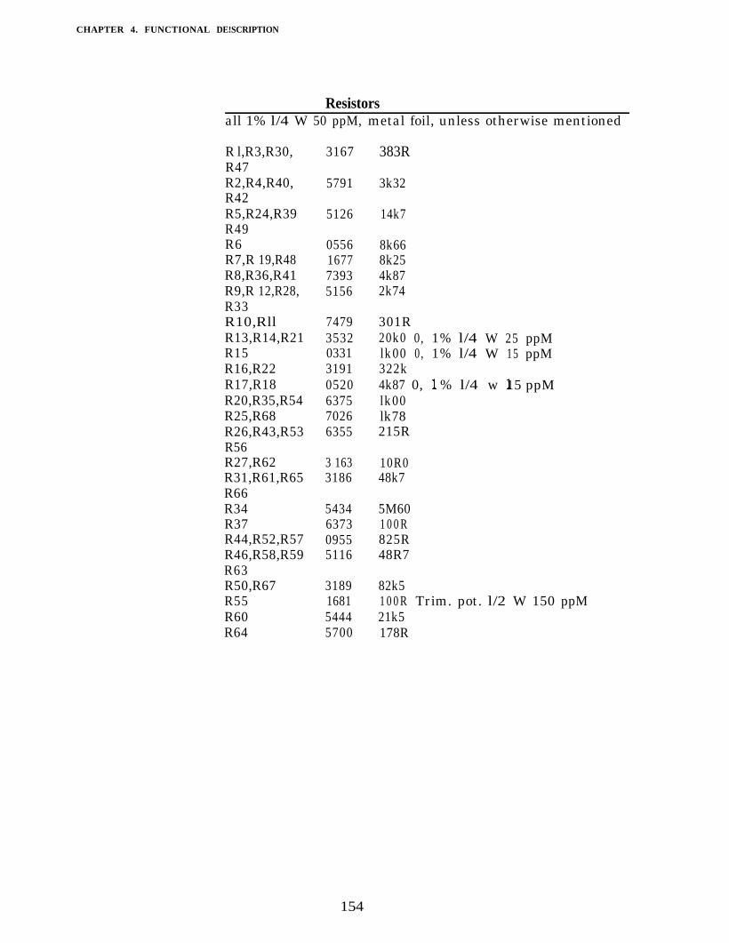
CHAPTER 4. FUNCTIONAL DE!SCRIPTION
Resistorsall 1% l/4 W 50 ppM, metal foil, unless otherwise mentioned
R l,R3,R30,R47R2,R4,R40,R42R5,R24,R39R49R6R7,R 19,R48R8,R36,R41R9,R 12,R28,R33R10,RllR13,R14,R21R15R16,R22R17,R18R20,R35,R54R25,R68R26,R43,R53R56R27,R62R31,R61,R65R66R34R37R44,R52,R57R46,R58,R59R63R50,R67R55R60R64
3167 383R
5791
5126 14k7
0556 8k661677 8k257393 4k875156 2k74
74793532033131910520637570266355
3 163 10R03186 48k7
5434 5M606373 100R0955 825R5116 48R7
3189168154445700
301R20k0 0, 1% l/4 W 25 ppMlk00 0, 1% l/4 W 15 ppM
% l/4 w 15 ppM322k4k87 0,lk00lk78215R
82k5100R Trim. pot. l/2 W 150 ppM21k5178R
3k32
154
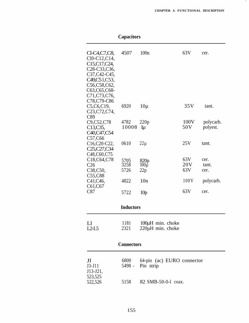
CHAPTER 4. FUNCTIONAL DESCRIPTION
Capacitors
Cl-C4,C7,C8,Cl0-C12,C14,C15,C17,C24,C28-C33,C36,C37,C42-C45,C49,C5 l,C53,C56,C58,C62,C63,C65,C68-C71,C73,C76,C78,C79-C86C5,C6,C19,C23,C72,C74,C89C9,C52,C78C13,C35,C40,C47,C54C57,C66C16,C20-C22,C25,C27,C34C48,C60,C75C18,C64,C78C26C38,C50,C55,C88C4 l,C46,C6 l,C67C87
4507 100n 63V cer.
6920 10µ 35V tant.
4782 220p 100V polycarb.10008 1µ 50V polyest.
0610 22µ 25V tant.
5705 820p3258 l00µ5726 22p
4822 10n
5722 10p
63V cer.20V tant.63V cer.
100V polycarb.
63V cer.
Inductors
LlL2-L5
1181 100µH min. choke2321 220µH min. choke
Connectors
JlJ3-J11J13-J21,523,525522,526
6800 64-pin (ac) EURO connector-5498 Pin strip
5158 82 SMB-50-0-l coax.
155
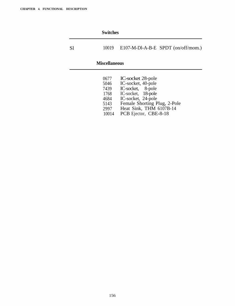
CHAPTER 4. FUNCTIONAL DESCRIPTION
Switches
Sl 10019 E107-M-Dl-A-B-E SPDT (on/off/mom.)
Miscellaneous
0677 IC-socket 28-pole5046 IC-socket, 40-pole7439 IC-socket, 8-pole1768 IC-socket, 18-pole4684 IC-socket, 24-pole5143 Female Shorting Plug, 2-Pole2997 Heat Sink, THM 6107B-1410014 PCB Ejector, CBE-8-18
156
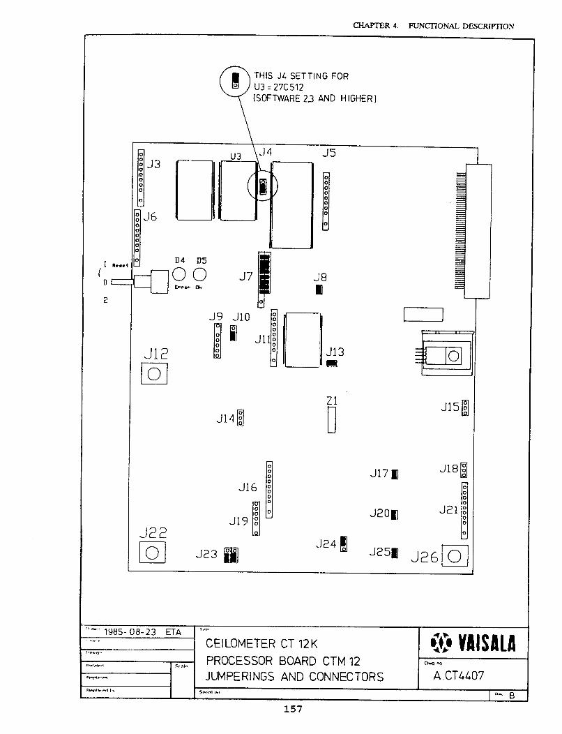
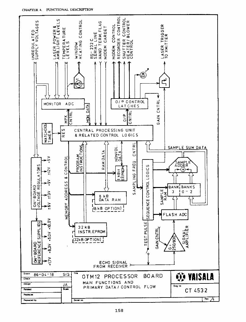
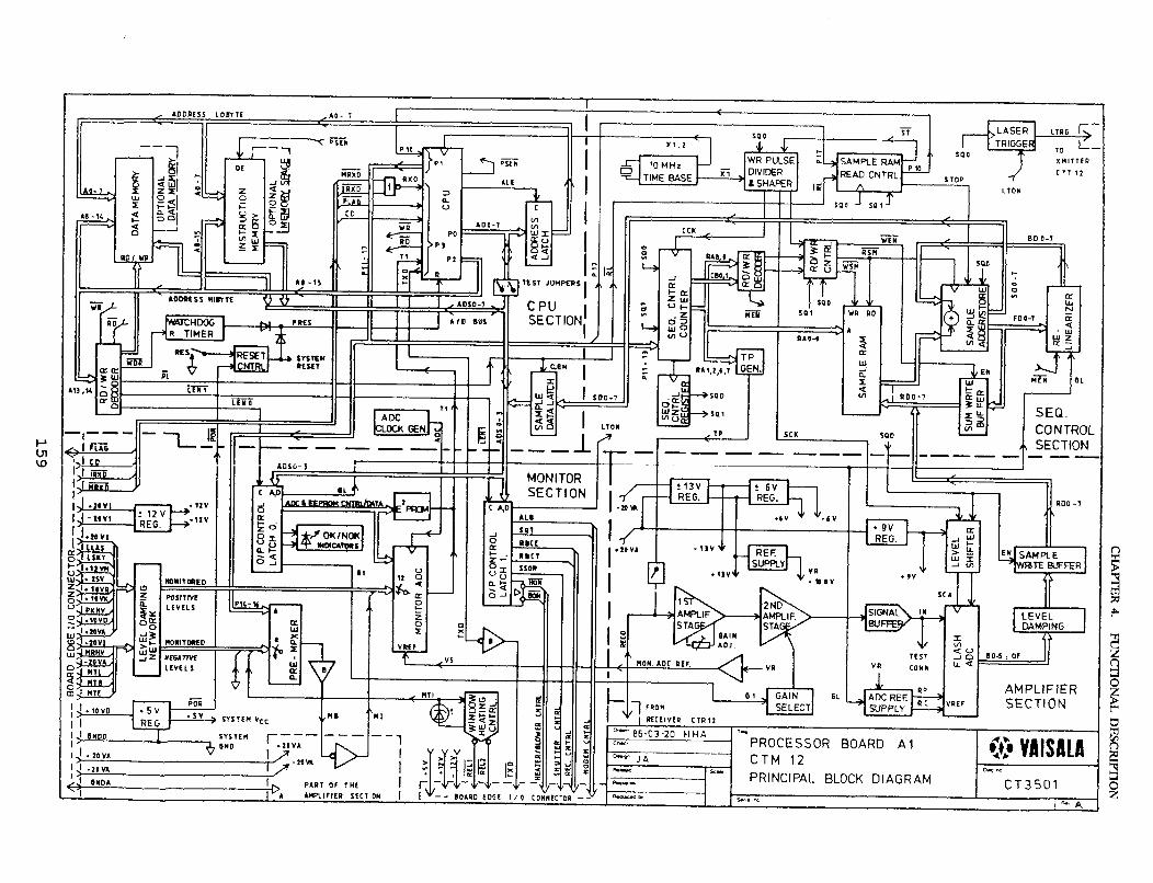
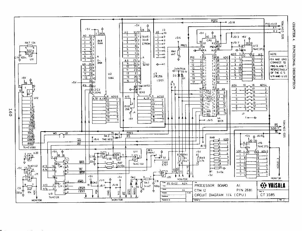
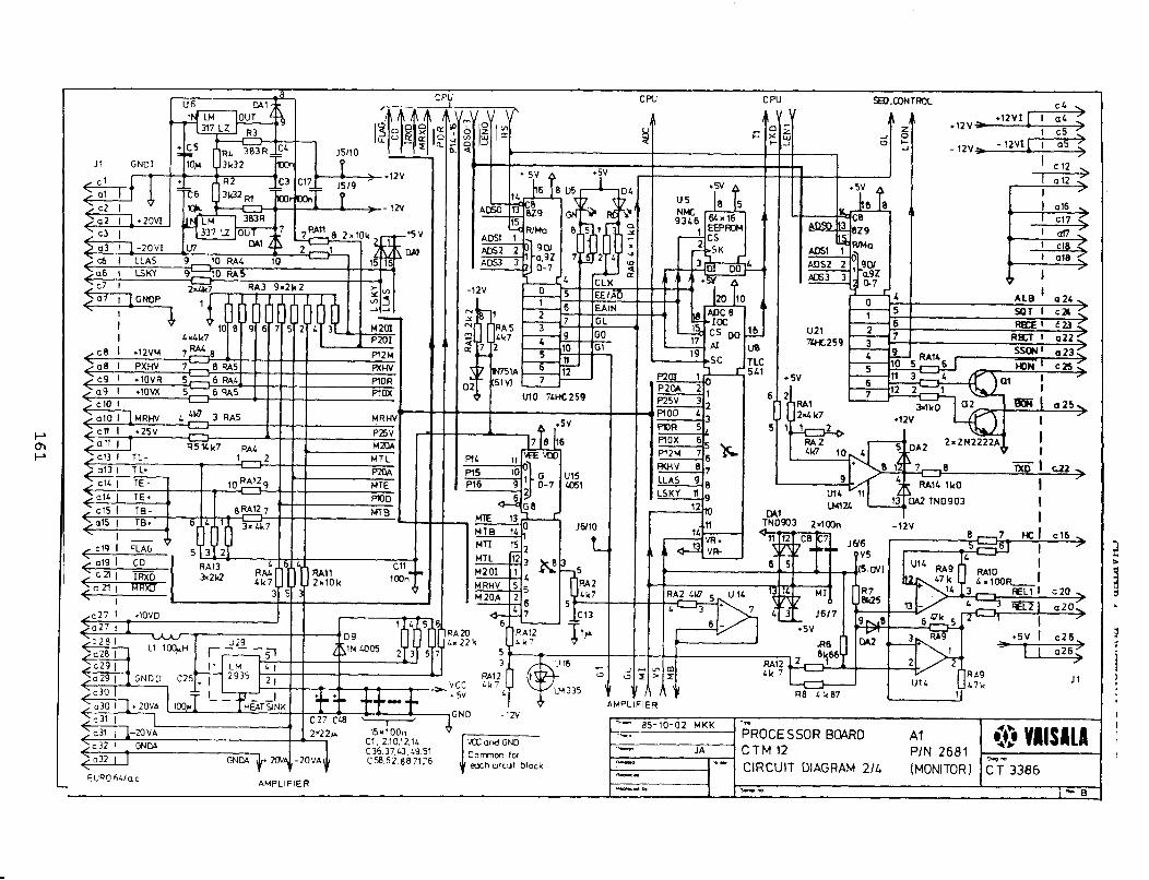
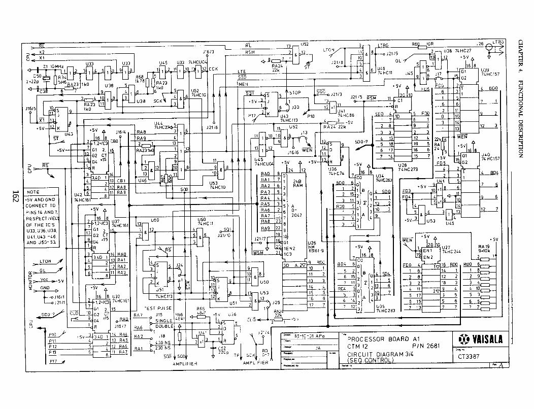
Hugh Black
162
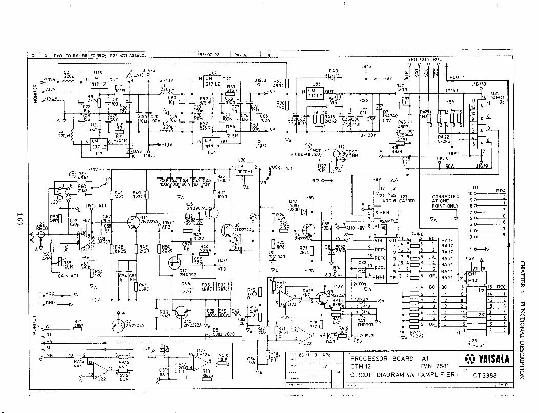
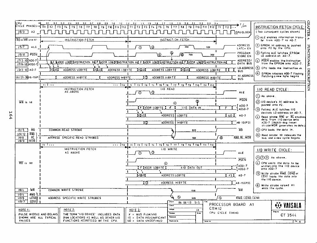
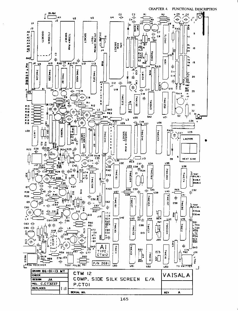
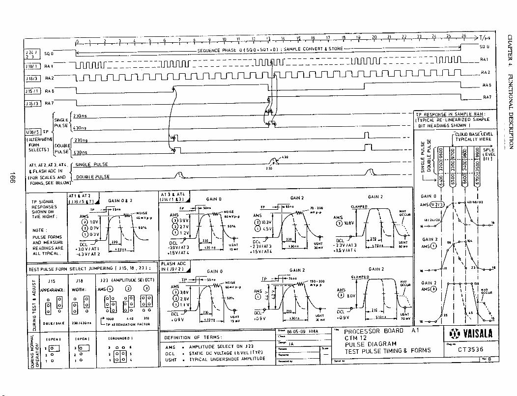
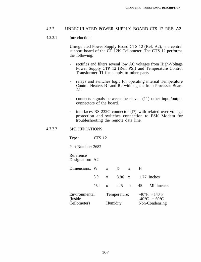
CHAPTER 4. FUNCTIONAL DESCRIPTION
4.3.2 UNREGULATED POWER SUPPLY BOARD CTS 12 REF. A2
4.3.2.1 Introduction
Unregulated Power Supply Board CTS 12 (Ref. A2), is a centralsupport board of the CT 12K Ceilometer. The CTS 12 performsthe following:
- rectifies and filters several low AC voltages from High-VoltagePower Supply CTP 12 (Ref. PSl) and Temperature ControlTransformer Tl for supply to other parts.
- relays and switches logic for operating internal TemperatureControl Heaters Rl and R2 with signals from Processor BoardAl.
- connects signals between the eleven (11) other input/outputconnectors of the board.
- interfaces RS-232C connector (J7) with related over-voltageprotection and switches connection to FSK Modem fortroubleshooting the remote data line.
4.3.2.2 SPECIFICATIONS
Type: CTS 12
Part Number: 2682
ReferenceDesignation: A2
Dimensions: W
5.9
150
Environmental(InsideCeilometer)
X D x H
X 8.86 x 1.77 Inches
X 225 x 45 Millimeters
Temperature: -40°F... + 140°F-40°C... + 60°C
Humidity: Non-Condensing
167
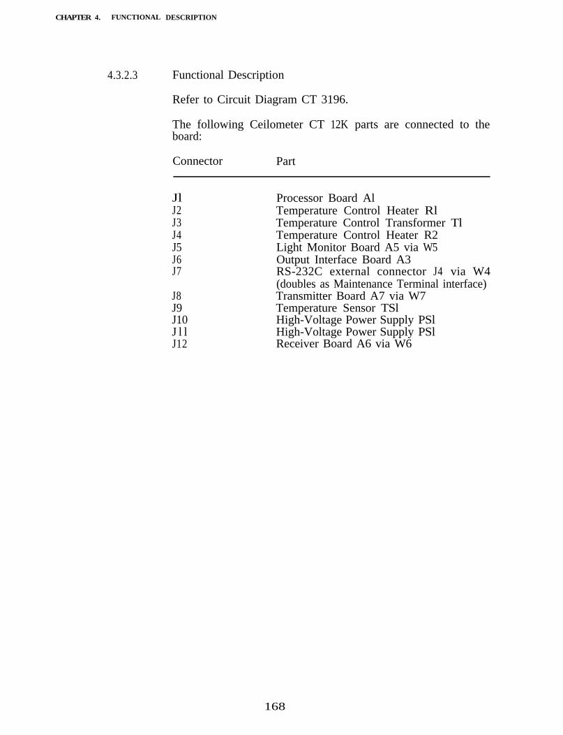
CHAPTER 4. FUNCTIONAL DESCRIPTION
4.3.2.3 Functional Description
Refer to Circuit Diagram CT 3196.
The following Ceilometer CT 12K parts are connected to theboard:
Connector Part
JlJ2J3J4J5J6J7
J8J9J10J l lJ12
Processor Board AlTemperature Control Heater RlTemperature Control Transformer TlTemperature Control Heater R2Light Monitor Board A5 via W5Output Interface Board A3RS-232C external connector J4 via W4(doubles as Maintenance Terminal interface)Transmitter Board A7 via W7Temperature Sensor TSlHigh-Voltage Power Supply PSlHigh-Voltage Power Supply PSlReceiver Board A6 via W6
168
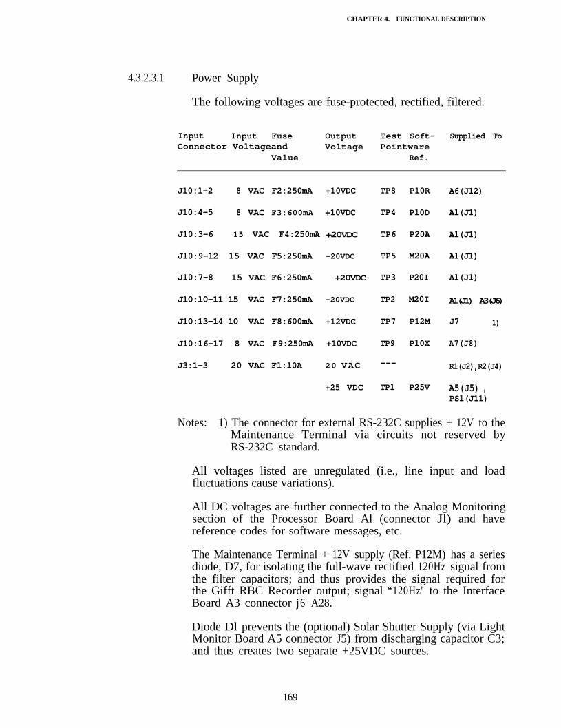
CHAPTER 4. FUNCTIONAL DESCRIPTION
4.3.2.3.1 Power Supply
The following voltages are fuse-protected, rectified, filtered.
Input Input Fuse Output Test Soft- Supplied ToConnector Voltageand Voltage Pointware
Value Ref.
Jl0:l-2 8 VAC F2:250mA
J10:4-5 8 VAC F3:600mA
J10:3-6 15 VAC F4:250mA
Jl0:9-12 15 VAC F5:250mA
+10VDC
+10VDC
+20VDC
-20VDC
J10:7-8 15 VAC F6:250mA
Jl0:l0-11 15 VAC F7:250mA
+20VDC
-20VDC
J10:13-14 10 VAC F8:600mA +12VDC
J10:16-17 8 VAC F9:250mA +10VDC
J3:1-3 20 VAC Fl:l0A 20 VAC
+25 VDC
TP8 Pl0R
TP4 Pl0D
TP6 P20A
TP5 M20A
TP3 P20I
TP2 M20I
TP7 P12M
TP9 Pl0X
---
TPl P25V
A6(J12)
Al(J1)
Al(J1)
Al(J1)
Al(J1)
A1(J1) A3(J6)
J7 1)
A7(J8)
R1(J2),R2(J4)
A5(J5) ,PSl(J11)
Notes: 1) The connector for external RS-232C supplies + 12V to theMaintenance Terminal via circuits not reserved byRS-232C standard.
All voltages listed are unregulated (i.e., line input and loadfluctuations cause variations).
All DC voltages are further connected to the Analog Monitoringsection of the Processor Board Al (connector Jl) and havereference codes for software messages, etc.
The Maintenance Terminal + 12V supply (Ref. P12M) has a seriesdiode, D7, for isolating the full-wave rectified 120Hz signal fromthe filter capacitors; and thus provides the signal required forthe Gifft RBC Recorder output; signal “120Hz' to the InterfaceBoard A3 connector j6 A28.
Diode Dl prevents the (optional) Solar Shutter Supply (via LightMonitor Board A5 connector J5) from discharging capacitor C3;and thus creates two separate +25VDC sources.
169
CHAPTER 4. FUNCTIONAL DESCRIPTION
4.3.2.3.2 Temperature Control
The RELl and REL2 signals are derived from an internaltemperature sensor through comparators and drivers, all locatedon the Processor Board Al.
At temperatures above approx. 20°C, neither relay is activatedand the Temperature Control Heaters Rl and R2 (connectors J2and J 4 are OFF.
At temperatures between approx. 0°C and 20°C, signal RELlactivates relay Kl. This will connect Rl and R2 in series acrossthe 20 VAC source from Tl (J3), and provide two lo-watt sourcesof power.
At temperatures below approx. O°C, signal REL2 activates relayK2 while signal RELl opens relay Kl. This will connect Rl andR2 in parallel1 across the 20 VAC from Tl (J3) and provide two40-watt sources of power.
By turning switch Sl to the “OFF” position, the relay driversrelease relays Kl and K2. This should be used only fortemporary maintenance or service operations.
Control signals RELl and REL2 operate without the interactionof the processor or software.
4.3.2.3.3 RS-232C Interface
The RS-232C signals come through connector J7, which is a D25Male type. There are two active signals which are the serialasynchronous data signals MTXD, pin 2, Data Transmitted fromCeilometer; and MRXD, pin 3, Data Received by Ceilometer.This corresponds with the Ceilometer appearing as Data TerminalEquipment (DTE).
Signals MRXD and MTXD are over-voltage protected by resistorsRl and R2, and transient zeners D5 and D6 which arebi-directional.
Data from the RS-232C Interface (MRXD) is “OR-ed” with inputdata both on the Processor Board Al and the Output InterfaceBoard A3.
170
CHAPTER 4. FUNCTIONAL DESCRIPTION
Data from Processor Board Al (TXD) is normally connected viaswitch S2 to the RS-232C interface as output data (MTXD).Switch S2 can also be set to connect the Ceilometer FSK lineinput data (IRXD) as output data (MTXD) of the RS-232Cinterface to enable communication from local RS-232C devicevia FSK line to the central site (e.g., for maintenance and servicepurposes).
Further, the RS-232C interface connector J7 carries a + 12Vsupply to the maintenance terminal, and a FLAG signal which,
. when activated, indicates the presence of a CTH 12 MaintenanceTerminal so that messages can be formatted appropriately. Thesesignals are positioned as circuits not reserved by the RS-232Cstandard.
171
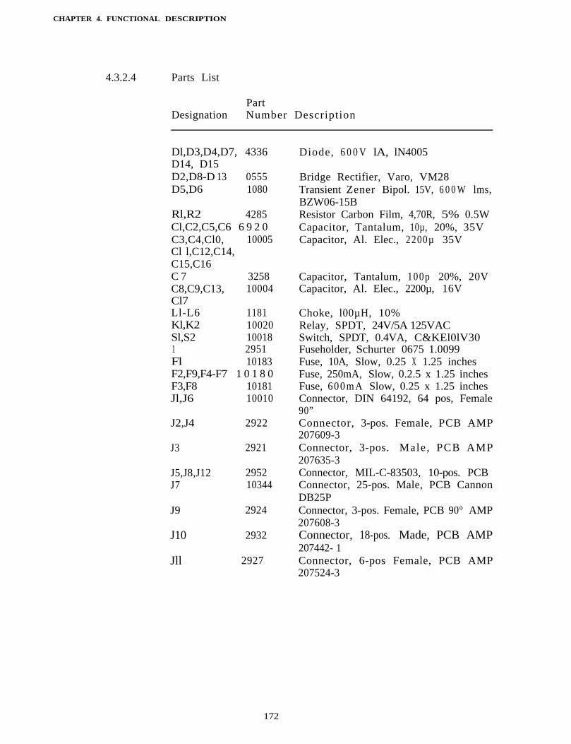
CHAPTER 4. FUNCTIONAL DESCRIPTION
4.3.2.4 Parts List
PartDesignation Number Description
Dl,D3,D4,D7, 4336D14, D15D2,D8-D 13 0555D5,D6 1080
Rl,R2 4285Cl,C2,C5,C6 6 9 2 0C3,C4,Cl0, 10005Cl l,C12,C14,C15,C16C 7 3258C8,C9,C13, 10004Cl7Ll-L6 1181Kl,K2 10020Sl,S2 100181 2951Fl 10183F2,F9,F4-F7 1 0 1 8 0F3,F8 10181Jl,J6 10010
J2,J4 2922
J3 2921
J5,J8,J12 2952J7 10344
J9 2924
J10 2932
Jll 2927
Diode, 6 0 0 V lA, lN4005
Bridge Rectifier, Varo, VM28Transient Zener Bipol. 15V, 6 0 0 W lms,BZW06-15BResistor Carbon Film, 4,70R, 5% 0.5WCapacitor, Tantalum, 10µ, 20%, 35VCapacitor, Al. Elec., 2200µ 35V
Capacitor, Tantalum, 100p 20%, 20VCapacitor, Al. Elec., 2200µ, 16V
Choke, l00µH, 10%Relay, SPDT, 24V/5A 125VACSwitch, SPDT, 0.4VA, C&KEl0lV30Fuseholder, Schurter 0675 1.0099Fuse, 10A, Slow, 0.25 X 1.25 inchesFuse, 250mA, Slow, 0.2.5 x 1.25 inchesFuse, 600mA Slow, 0.25 x 1.25 inchesConnector, DIN 64192, 64 pos, Female90”Connector, 3-pos. Female, PCB AMP207609-3Connector, 3-pos. Male , PCB AMP207635-3Connector, MIL-C-83503, 10-pos. PCBConnector, 25-pos. Male, PCB CannonDB25PConnector, 3-pos. Female, PCB 90° AMP207608-3Connector, 18-pos. Made, PCB AMP207442- 1Connector, 6-pos Female, PCB AMP207524-3
172
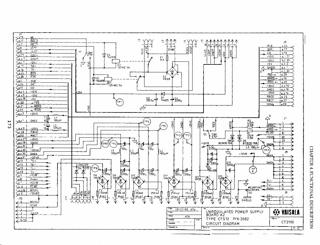
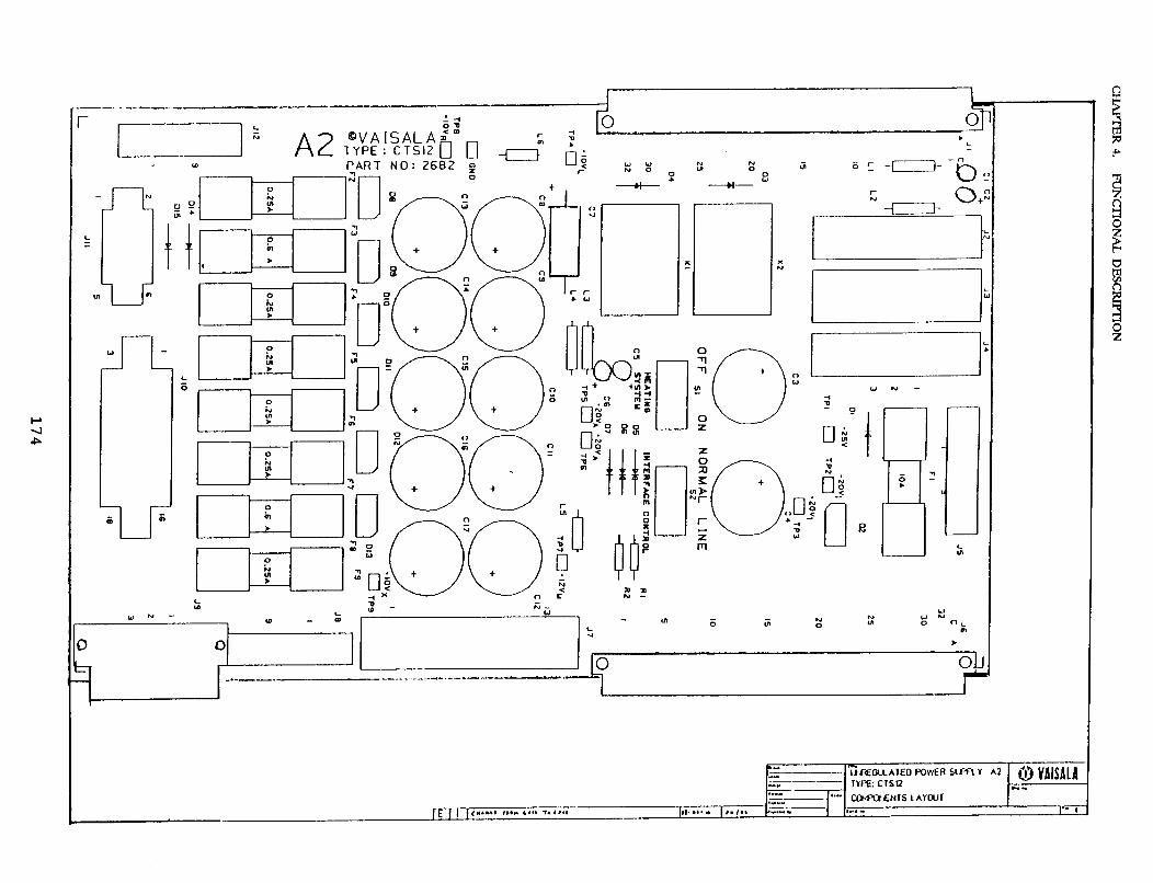
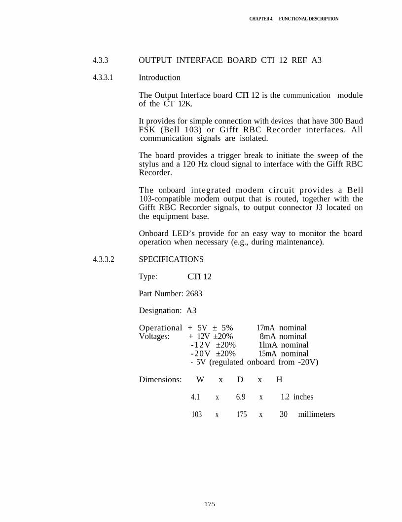
CHAPTER 4. FUNCTIONAL DESCRIPTION
4.3.3
4.3.3.1
OUTPUT INTERFACE BOARD CTI 12 REF A3
Introduction
The Output Interface board CTI 12 is the communication moduleof the CT 12K.
It provides for simple connection with devices that have 300 BaudFSK (Bell 103) or Gifft RBC Recorder interfaces. Allcommunication signals are isolated.
The board provides a trigger break to initiate the sweep of thestylus and a 120 Hz cloud signal to interface with the Gifft RBCRecorder.
The onboard integrated modem circuit provides a Bell103-compatible modem output that is routed, together with theGifft RBC Recorder signals, to output connector J3 located onthe equipment base.
Onboard LED’s provide for an easy way to monitor the boardoperation when necessary (e.g., during maintenance).
4.3.3.2 SPECIFICATIONS
Type: CTI 12
Part Number: 2683
Designation: A3
Operational + 5V ± 5% 17mA nominalVoltages: + 12V ±20% 8mA nominal
-12V ±20% 1lmA nominal-20V ±20% 15mA nominal- 5V (regulated onboard from -20V)
Dimensions: W x D x H
4.1 x 6.9 x 1.2 inches
103 x 175 x 30 millimeters
175
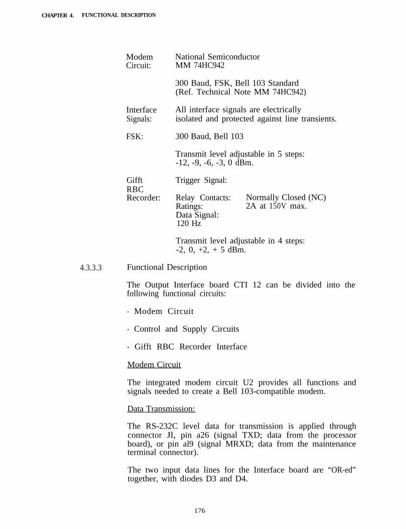
CHAPTER 4. FUNCTIONAL DESCRIPTION
Modem National SemiconductorCircuit: MM 74HC942
300 Baud, FSK, Bell 103 Standard(Ref. Technical Note MM 74HC942)
InterfaceSignals:
FSK:
All interface signals are electricallyisolated and protected against line transients.
300 Baud, Bell 103
Transmit level adjustable in 5 steps:-12, -9, -6, -3, 0 dBm.
GifftRBCRecorder:
Trigger Signal:
Relay Contacts:Ratings:Data Signal:120 Hz
Normally Closed (NC)2A at 150V max.
Transmit level adjustable in 4 steps:-2, 0, +2, + 5 dBm.
4.3.3.3 Functional Description
The Output Interface board CTI 12 can be divided into thefollowing functional circuits:
- Modem Circuit
- Control and Supply Circuits
- Gifft RBC Recorder Interface
Modem Circuit
The integrated modem circuit U2 provides all functions andsignals needed to create a Bell 103-compatible modem.
Data Transmission:
The RS-232C level data for transmission is applied throughconnector Jl, pin a26 (signal TXD; data from the processorboard), or pin al9 (signal MRXD; data from the maintenanceterminal connector).
The two input data lines for the Interface board are “OR-ed”together, with diodes D3 and D4.
176
CHAPTER 4. FUNCTIONAL DESCRIPTION
The signal is limited to 5V levels by the resistors of resistor arrayRA3 (pins 3-4 and 7-8). The signal is inverted by Ul and appliedto the input pin TXD of the modem circuit U2.
The monitoring LED D10, ‘TXD,” indicates the presence of dataat the TXD-input of the modem circuit U2.
The modem circuit U2 modulates internally the input serial dataof 300 Baud and outputs the modulated data via pin TXA.
The modulated data is transmitted through the couplingtransformer T2 (600 ohms) and output via connector J2, pins 1and 2 (signals MOD1 and MOD2).
The zener diodes D15 and D16 protect the modem circuit U2from line transients.
The transmit level of the modem output can be adjusted in therange of -12 dBm...0dBm by jumper J8. For the adjustment ofthe line transmit level, refer to jumper setting table in the CircuitDiagram CT 2277.
Data Recention;
The line signal, through coupling transformer T2, produces avoltage across resistor R18 sensed by the input terminals RXA1and RXA2 of the modem circuit.
The demodulation is performed and the serial data is availableat the output pin RXD of the modem circuit. The 5V level datais converted to RS-232C levels and inverted by transistors Q4, Q5,and diodes D5 and D6.
The LED Dll, “RXD,” indicates the presence of data after thedemodulation by the modem circuit at transistor Q5. The datais available for the processor via connector Jl, pin a25 (signalIRXD).
The presence of the carrier frequency is indicated by LED D12,“CD,” and sensed by the processor via connector Jl, pin a18(signal CD).
177
CHAPTER 4. FUNCTIONAL DESCRIPTION
Control and S u p p l y Circuits
The “Originate/Answer” mode can be selected by jumper J7,according to the jumper setting table in Circuit Diagram CT 2277.
Signal SQT of connector Jl, pm a24, enables the processor tocontrol the modulation of the modem circuit U2. The modulationis disabled, when signal SQT is held “high,” and it also preventsthe data transmission to the modem circuit communication lines.
The function of the modem circuit U2 can be tested by thecontrol signal ALB at connector Jl, pin a24. The processor cantest the operation of the modulation/demodulation circuits withsignal ALB in a “high” condition. The data from the TXD inputis then echoed back from the RXD output of the modem circuitu2.
The “power-down” mode of the modem circuit can be activated,when signals SQT and ALB are simultaneously held “high” by theprocessor.
The basic clock frequency of 3.58 MHz for modem circuit U2 isgenerated by crystal Z1.
The onboard -5V regulator, U3, uses the -20V voltage suppliedthrough connector Jl, pins al4 and c14. The output voltage ofthe regulator is adjusted by resistor R16 and R17.
The +5V voltage supplied thorugh connector Jl, points a2 andc2, is filtered by capacitors Cl5 and C16, and inductor L2, toprevent possible interference from entering the power supply.
178
CHAPTER 4. FUNCTIONAL DESCRIPTION
The Gifft RBC Recorder Interface
The general operating principle of the recorder is to produce linesor dots whenever backscattered energy or clouds are detected bythe Ceilometer. The dots are generated by continuously sweepingthe recorder pen, over dry electrosensitive recorder paper.
The Trigger Break signal:
The sweep of the Gifft RBC Recorder stylus is started by the pro-cessor’s RBC-message output routine through relay Kl.
The processor board provides an active-high start pulse throughconnector Jl, pin a27 (signal RBCT). The pulse width is 80 msnominally.
The signal RBCT switches transistor Q3 “on.” The relay contactis opened when RBCT is held ‘high”, active).
The “high-low“ transition of signal RBCT closes the relay contact.A regulated current of 4mA (from the Field Junction Box of theGifft Recorder) passes through the relay contact to the recorder(open circuit voltage approximately 90V).
When signal RBCT is held “high,” LED D1.3, "RBCT," is on.
The inductive transients caused by the coil of Kl are suppressedby diode D7.
The Trigger Break signal for the Recorder is available at outputconnector J2, pins 9 and 10 (signals RBCTl and RBCC2).
179
CHAPTER 4. FUNCTIONAL DESCRIPTION
The Cloud Data Signal
A modulating signal referred to as “120 Hz” is applied throughconnector Jl, pin a28. The frequency of the “120 Hz” signal isobtained from the Power Line supply. The signal is filtered byinductor Ll, resistor Rl, and capacitor C3.
The transmit level of the signal can be adjusted by jumper J3 inthe range of -2dBm... + 5dBm. Refer to the “jumper setting table”of the Circuit Diagram CT 2277.
When the recorder sweep has reached a position proportional tothe height of a cloud hit, signal RBCE is raised “high” by theprocessor. This signal is applied through Jl, pin a22.
The RBCE signal “high” switches the modulating “120 Hz” signalvia transistors Ql and Q2, and the coupling transformer Tl, tothe output connector Jl, pins 5 and 6 (signals RBCEl andRBCE2).
LED D14, “RBCE,” indicates the presence of the cloud data signalat the output of gating transistor Ql. Line transients aresuppressed by transient zeners Dl and D2.
1 8 0
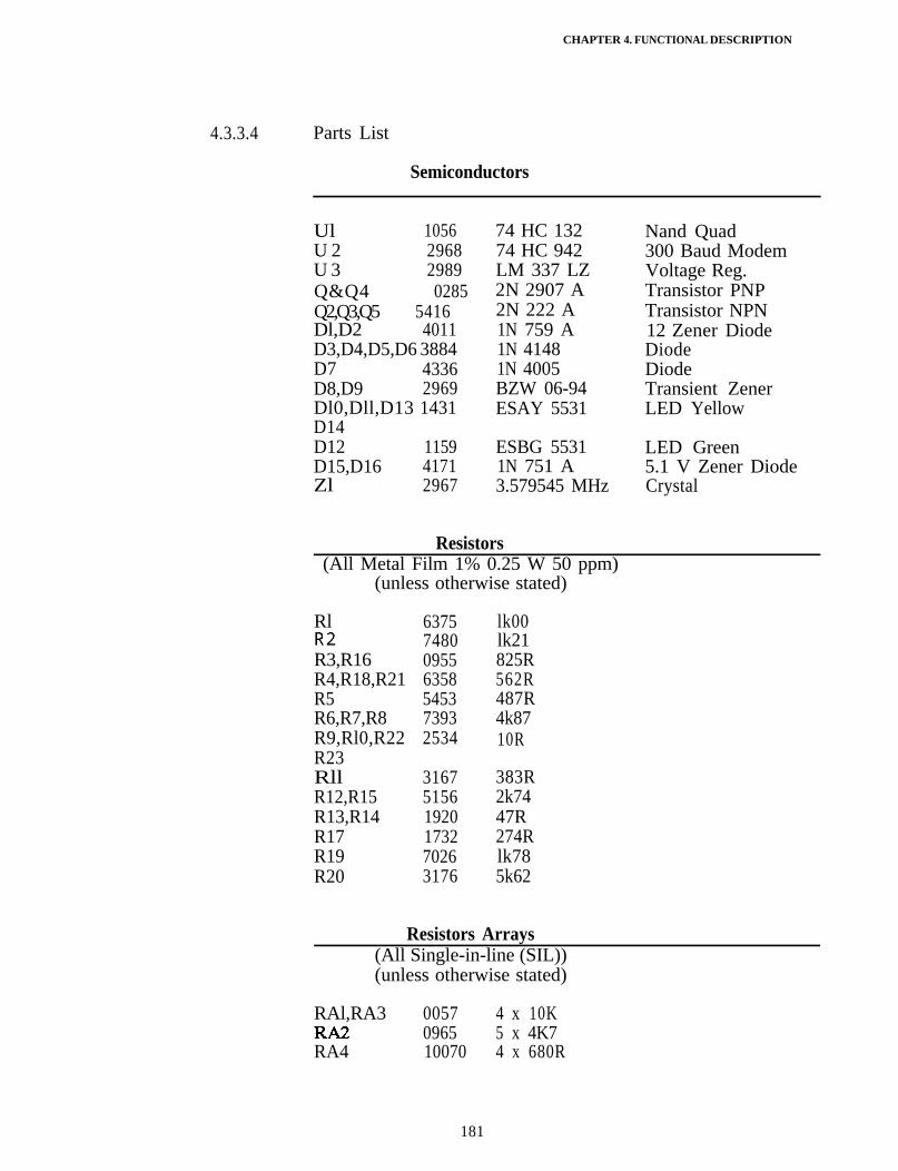
CHAPTER 4. FUNCTIONAL DESCRIPTION
4.3.3.4 Parts List
Semiconductors
Ul 1056U 2 2968U 3 2989Q&Q4 0285Q2,Q3,Q5 5416Dl,D2 4011D3,D4,D5,D6 3884D7 4336D8,D9 2969Dl0,Dll,D13 1431D14D12 1159D15,D16 4171Zl 2967
74 HC 132 Nand Quad74 HC 942 300 Baud ModemLM 337 LZ Voltage Reg.2N 2907 A Transistor PNP2N 222 A Transistor NPN1N 759 A 12 Zener Diode1N 4148 Diode1N 4005 DiodeBZW 06-94 Transient ZenerESAY 5531 LED Yellow
ESBG 55311N 751 A3.579545 MHz
LED Green5.1 V Zener DiodeCrystal
Resistors(All Metal Film 1% 0.25 W 50 ppm)
(unless otherwise stated)
Rl
R3,R16R4,R18,R21R5R6,R7,R8R9,Rl0,R22R23RllR12,R15R13,R14R17R19R20
6375 lk007480 lk210955 825R6358 562R5453 487R7393 4k872534 10R
3167 383R5156 2k741920 47R1732 274R7026 lk783176 5k62
Resistors Arrays(All Single-in-line (SIL))(unless otherwise stated)
RAl,RA3 0057 4 x 10K0965 5 x 4K7
RA4 10070 4 x 680R
181
Archive
R2
Archive
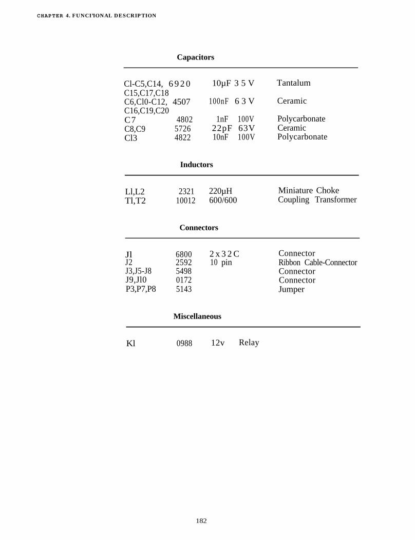
CHAPTER 4. FUNCI’IONAL DESCRIPTION
Capacitors
Cl-C5,C14, 6 9 2 0C15,C17,C18C6,Cl0-C12, 4507C16,C19,C20C7 4802C8,C9 5726Cl3 4822
10µF 3 5 V Tantalum
100nF 6 3 V Ceramic
1nF 100V Polycarbonate22pF 63V Ceramic10nF 100V Polycarbonate
Inductors
Ll,L2Tl,T2
2321 220µH Miniature Choke10012 600/600 Coupling Transformer
Connectors
Jl 6800J2 2592J3,J5-J8 5498J9,Jl0 0172P3,P7,P8 5143
2 x 3 2 C10 pin
ConnectorRibbon Cable-ConnectorConnectorConnectorJumper
Miscellaneous
Kl 0988 12v Relay
182
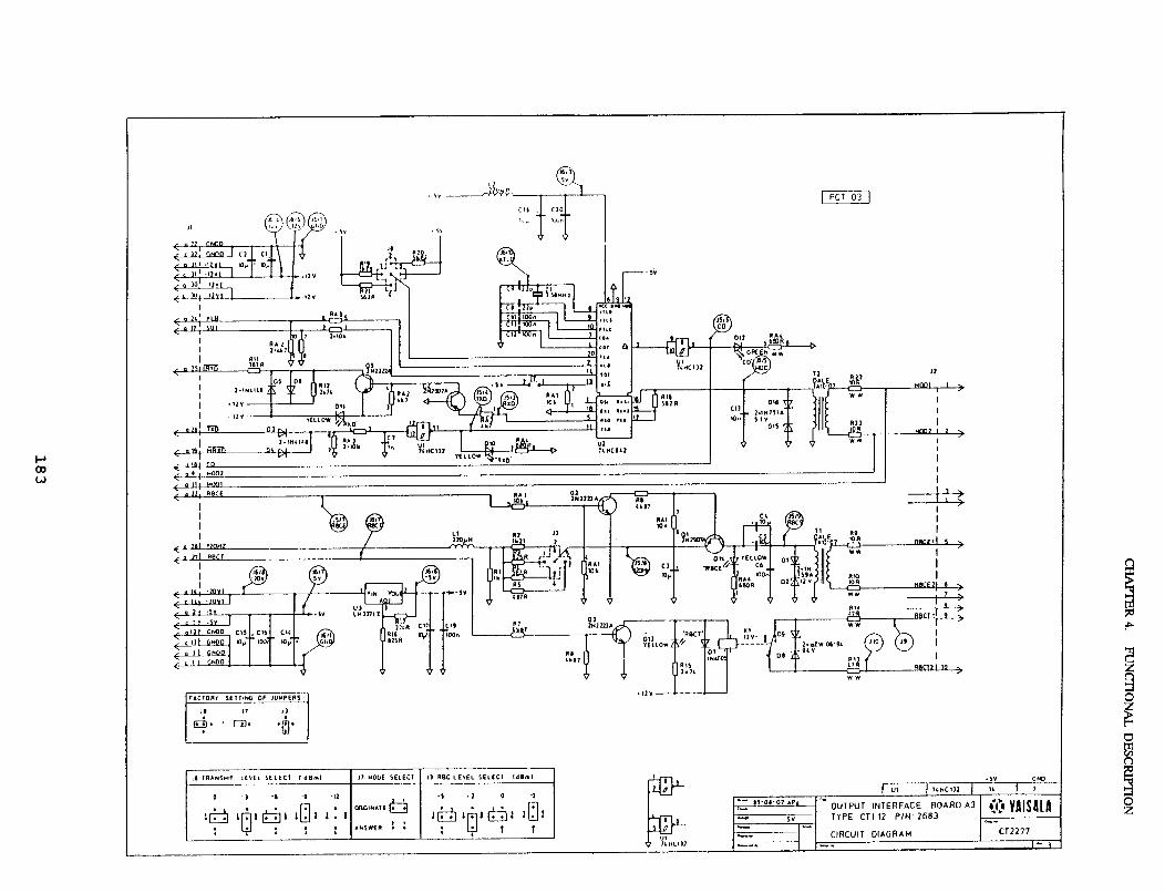
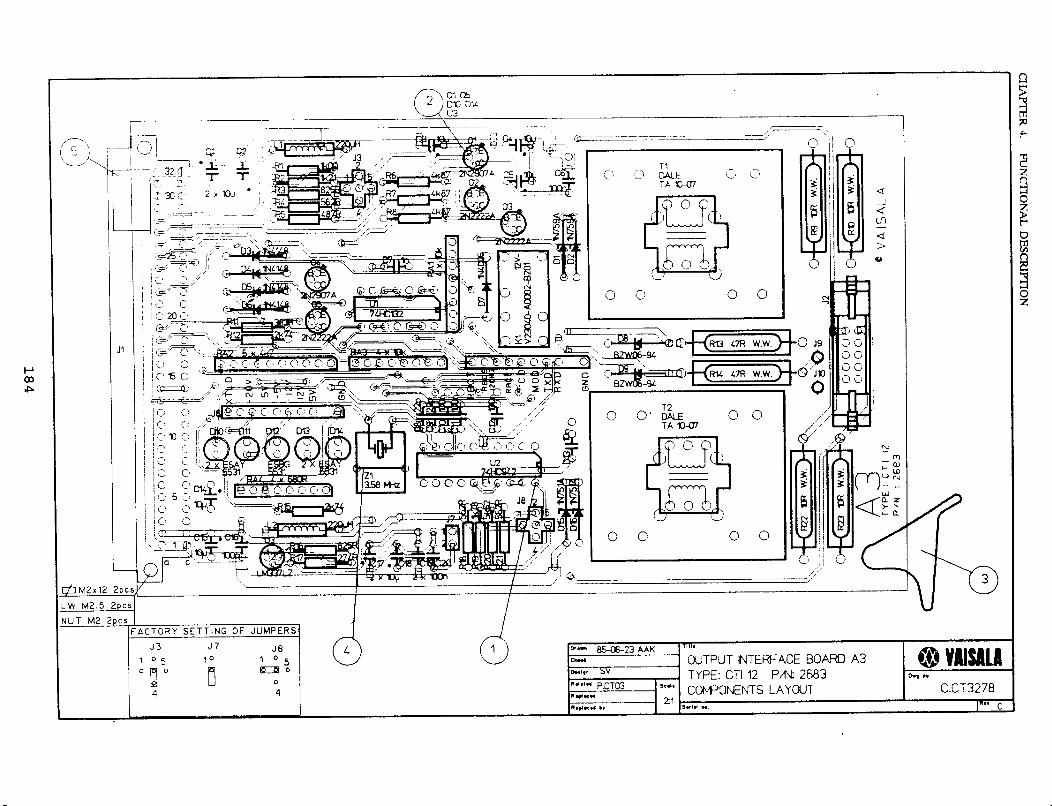
CHAPTER 4. FUNCTIONAL DESCRIPTION
4.3.4 LIGHT MONITOR BOARD CTL 13 REF A5
4.3.4.1 Introduction
The Light Monitor Board of Ceilometer CT 12K is placedbetween the laser transmitter lens and the instrument coverwindow, in a position which minimizes attenuation of transmittedlaser power (refer to CTL 13 Assembly A.CT 3410).
It contains the following circuits (Ref. Circuit Diagram CT 3564):
Laser Power Monitor. Its silicon PIN photodiode is pointeddown toward the collimated laser beam at a position whichbest represents the average power of the non-uniform beam.
- Skv Light Monitor. Its silicon PIN photodiode is pointedupward and its field-of-view is limited to a detection angle ofapproximately +5.7° from vertical. Its signal is used both bythe Solar Shutter circuitry and by the processor, for monitoringpurposes.
- Solar Shutter Driver. This circuit drives the optional externalSolar Shutter Kl and shuts its flap for protection of the laserdiode from focused sunlight, if the signal from the Sky LightMonitor should exceed the voltage set by a trimpot. It isfail-safe in operation (i.e., when no power is supplied, the flapis shut). The operation is also self-contained so that noprocessor activity is required for shutting.
- Voltage Regulator for providing an internal regulated + 17 Vsupply for the measurement circuits.
4.3.4.2 Specifications
Type: CTL 13 Light Monitor BoardPart Number: 10322Des igna t ion : A5Supply: 22V...30V, 20mA typ. without shutter
650mA typ. with shutterDimensions: W x D x H
6.7 x 2.1 x 0.9 inches
170 x 54 x 23 millimeters
185
CHAPTER 4. FUNCTIONAL DESCRITPION
Laser Power V(LLAS) = 0.9V...4.5V at nominal laser power
Monitor:Filtering Time constant 100msFactory calibrated;transmitter specific 100% value to beinput in CT 12K for parameter LNOR
sky LightMonitor:
V(LSKY) = 1 V/16 W (typ.) from solid angle0.03 srad
Bandwidth 300 nm...ll00 nmFiltering Time Constant 0.2 s
Solar Shutter Factory set trip level 32 W (typ.) fromDriver: solid angle 0.03 srad
Hysteresis 16 W (typ.)
4.3.4.3 Functional Description
Laser Power Monitor
Laser power is detected by photodiode Dl which, in its normaloperating position, is pointed downward toward the lasertransmitter. Dl converts the short, powerful light pulses tocurrent pulses. These are transferred via Schottky diode D2 tocapacitor C2 (100nF). The charge collected by capacitor C2discharges via resistor R3 (1 Megohm). The time constant C2x R3 is 100 ms; thus, the laser pulse frequency which is 620Hz...1120 Hz (1.6 ms...0.9 ms) will be converted to a DC voltageacross R3, the magnitude of which will equal, in volts, the averageof the pulse current in microamperes. The voltage will never riseso high that the negative bias across photodiode Dl will besignificantly reduced.
Ambient light current which, at peak magnitude, is much less thanthe laser pulse current, passes to ground via resistor Rl. DiodeD2 prevents it from being transferred to capacitor C2 because ofthe positive bias required for it to conduct (0.3V...0.4V) in allpractical cases exceeding the voltage across Rl. On the otherhand, Rl is big enough not to create any considerable error inactual laser pulse current measurement.
Capacitor Cl and resistor R2 block the sharp current pulse fromthe rest of the circuitry.
Op-amp l/4 Ul (LM124) amplifies the voltage across R3 to alevel suitable for measurement by the processor board monitorA/D-converter (0V...5V). Gain is factory set.
186
C H A P T E R FUNCTIONAL DESCRIPTION
The resulting signal can be measured at test point TPl. It alsodrives red LED D4. It is brought out at connector Jl, pin 10.It is referenced in the processor software as LLAS and measuredby monitor A/D-converter channel 8 (analog monitoring commandAN 8 or AN LLAS).
Because of the variation between individual photodiodes, eachlaser power monitor is factory calibrated. The norm value whichcorresponds to 100% of nominal laser power is marked as thevalue of parameter LNOR on the Ceilometer Transmitter board.This value is to be input in the processor prior to use.
Skv Light Monitor
Sky light power is monitored by upward-pointing photodiode D3through an aperture which limits the viewing solid-angle toapproximately 0.03 srad. Deflection from vertical is approximately5.7” average non-circular cross-section because of the rectangulardetector chip.
Its sensitivity is approximately 0.4 A/W. Pointed directly towardthe sun in a clear-atmosphere sky (approximately 1200 W/m2)produces a current of l.lmA typically. A clear blue sky producesa current of l0µA typically, and indoor conditions produce lessthan 1µA.
The current produced by the sky light in photodiode D3 isconverted to a voltage across resistor R4 (21k4) and filtered bycapacitor C3 (10µF) which yields a time constant of 214 ms. Thevoltage is buffered by voltage follower l/4 Ul, the output ofwhich can be measured at test point TP2. It is fed to the SolarShutter Driver circuitry, and to the board output at connector Jl,pin 9. It is referenced as LSKY and may be monitored as analogchannel 9 (monitor command AN9 or AN LSKY).
The voltage range of the monitor A/D-converter of the processorboard, 0V...5V will yield a useful sky light power range of0W/m2...80W/m2 based on assumption of clear, direct sun being1200 W/m2.
187
CHAPTER 4. FUNCTIONAL DESCRIPTION
Solar Shutter Driver
The voltage output of the Sky Light Monitor is brought tocomparator l/4 Ul, pin 13. Its trip voltage is set by trimpot R13to a value which is measured at test point TP4. Standard valueis 2.0V corresponding to a sky light power of approximately 32W which provides for adequate margin with respect to all sourcesof inaccuracy regarding the protection of the laser transmitteragainst focused sunlight from zenith.
Positive feedback resistors R10 and Rll create a hysteresis of 1volt at comparator input, pin 12, corresponding to a light powerof approximately 16 W/m2. Thus, the trip point must alwaysexceed the l-volt value.
The output of the comparator Ul, pin 14, is high (+ 15V) whensky light power is low (i.e., below the trip point) and the outputis low when sky light power is high. This output drives the SolarShutter Darlington transistor Q2, the design being such that theSolar Shutter Solenoid (Kl) has to be energized to be open(collector of Q2 “low”) and de-energized to be closed (voltage ofcollector Q2 close to +24 V supply). This fail-safe mode ofoperation provides for high-reliability protection in all cases ofpower failure and most cases of equipment (component) failure.Resistor R12 provides for safety should the wiper of trimpot R13fail.
The processor can close the solar shutter with signal SSON (Jl,pin 5) by raising it “high,” thereby switching transistor Ql “on”which will short the base of Q2 and prevent it from keepingshutter Kl energized. The processor cannot force the shutter tostay open should the light power detected by D3 cause a voltageexceeding the set point at TP4.
The shutter driver circuitry has a separate current return ground(GNDS) in order not to disturb the measurements. These havea low current return ground (GNDP) which is routed separatelyto the common ground. D i o d e s D5 a n d D 6 p r o t e c t t h ecomponents in case of failure of any ground lead.
Voltage Regulator
The measurement circuits of the board are powered through anon-board, 3-lead voltage regulator U2 (LM 317LZ). Its supplyis from the board’s +24V and resistors R14 and R15 determinethe level of the internal supply voltage, + 17V ± 1V. CapacitorsC4 and C5 provide filtering.
188
CHAPTER 4. FUNCTIONAL DESCRIPTION
4.3.4.4 Parts List
Semiconductors
Ul 2456u 2 1016Ql 5416Q2 1384Dl,D3 2973D2 4685D4 5429D5,D6,D7 4336
LM124LM3 17LZ2N 2222ATIP 120UDT PIN 3CDHP 5082-2800HP 5082-4655lN4005
Quad Op AmplifierVoltage RegulatorNPN TransistorNPN DarlingtonPhotodiodeSchottky DiodeLED RedDiode
Resistors(all resistors Metal Film 1% 50 ppm 0.25 W)
(unless otherwise stated)
R15R6,R 13R8,R12R2,R 14R3,Rl0RllR5R4
5156 2k746372 10k Potentiometer5388 10k6355 215R6627 1MO0791 68kl5453 487R5444 21k5
Resistor Array
RA1 2960 4 x 2k2
Capacitors
Cl,C2,C4
C3,C5
0977 1OOnF 6 3 V
0009 10µF 2 5 V
Polyester
Tantalum
Connectors
Jl 2963J2 2924
MIL-C-83503, 10 pos., Male, 90”Amp Metrimate 207608-3, 3 pos.,Header, Female PCB, 90”
189
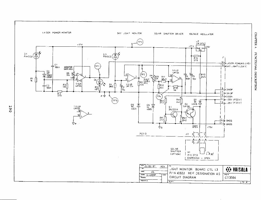
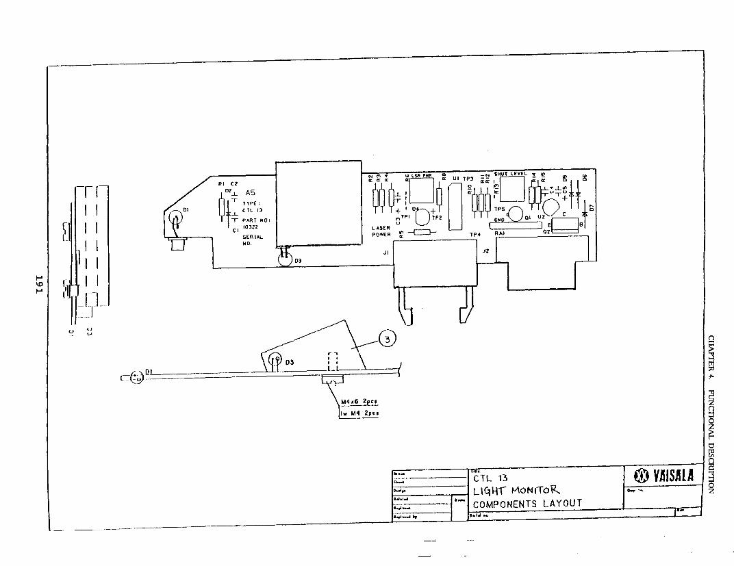
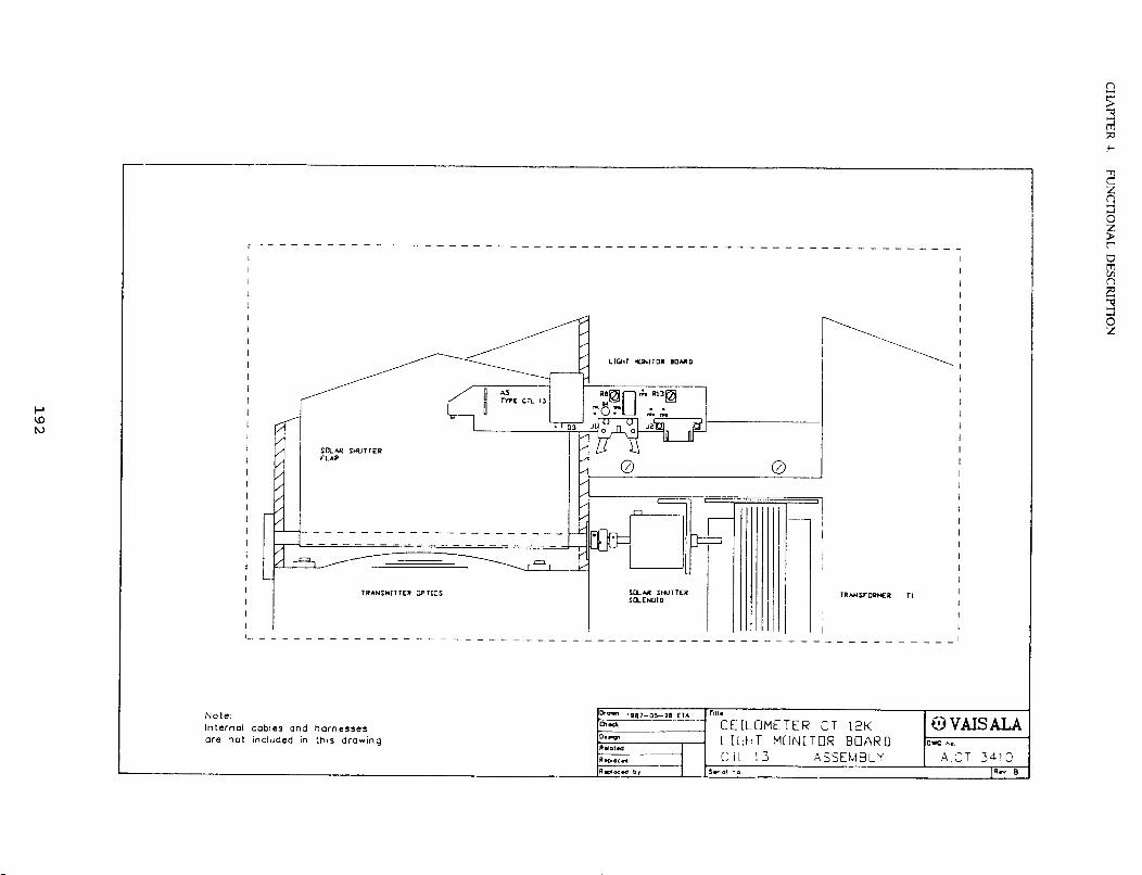
CHAPTER 4. FUNCTIONAL DESCRIPTION
4.3.5 RECEIVER BOARD CTR 13
4.3.5.1 Introduction
The Receiver Board CTR 13 contains the photodiode that detectsthe reflections from any obstructions (normally clouds) in the pathof the transmitted laser pulse.
The reflections are detected by the silicon avalanche photodiodelocated at the focal point of the receiver optics.
These focused reflections from the field-of-view of the receiverare converted to current in the reverse-biased photodiode.
The change of current is sensed and amplified by the onboardcircuits to provide a suitable output for the Processor Board CTM12 (Ref. Al).
The bias voltage of the photodiode is supplied from theHigh-Voltage Power Supply (Ref. PSl), regulated andtemperature-compensated on the Receiver Board, and monitoredby circuitry on the Processor Board.
The photodiode sensitivity is temperature-dependent. This iscompensated for by a temperature-dependent control of the biasvoltage.
The value of the bias voltage should be checked at maintenanceor service of the Receiver. It is factory-adjusted to a value foundon a sticker on the board at room temperature, giving theReceiver a nominal responsivity of 40 A/W. The actual biasvoltage then varies by a factor of 1.3 V/°F (2.3 V/°C) dependingon the actual temperature, giving it a constant responsivity.
The positioning of the photodiode and its mounting hardware onthe receiver board is extremely critical and is held to tightmanufacturing tolerances. This assumes field interchangeabilityof all receiver boards without the requirement of opticalrealignments.
193
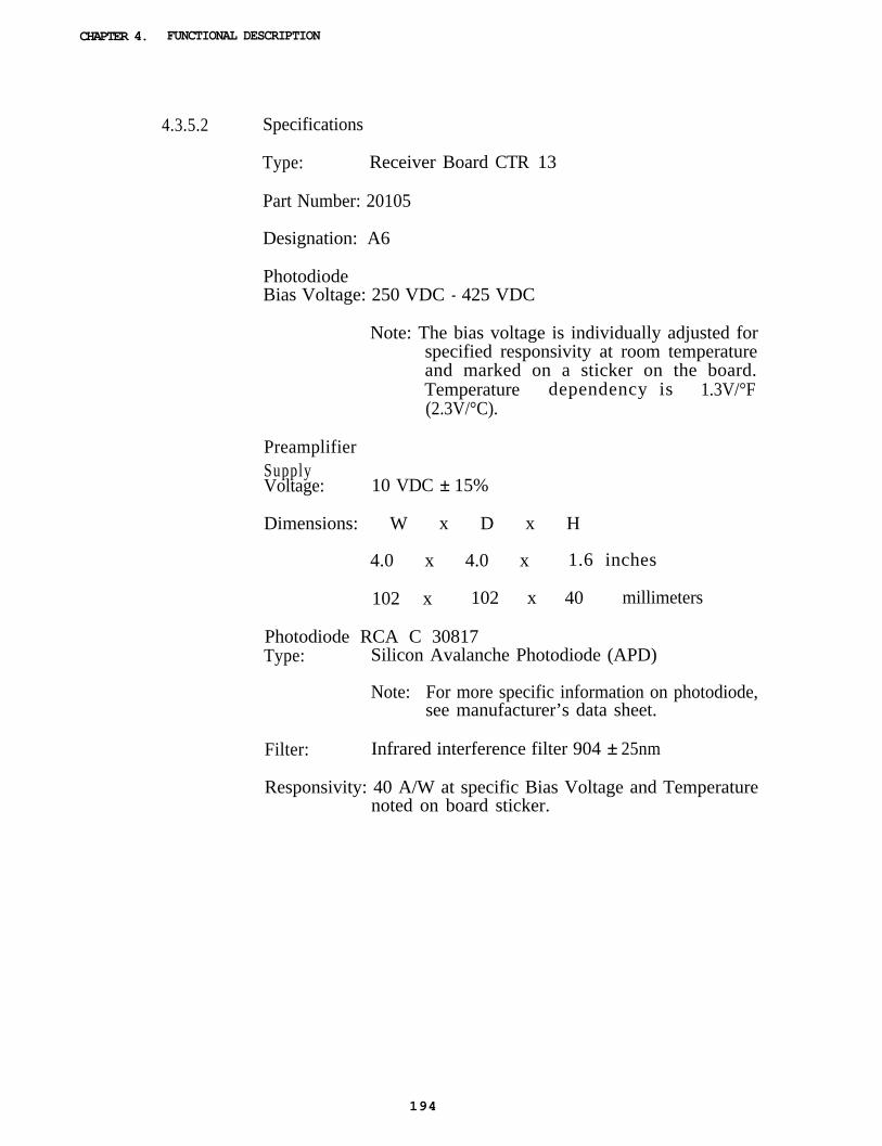
CHAPTER 4. FUNCTIONAL DESCRIPTION
4.3.5.2 Specifications
Type: Receiver Board CTR 13
Part Number: 20105
Designation: A6
PhotodiodeBias Voltage: 250 VDC - 425 VDC
Note: The bias voltage is individually adjusted forspecified responsivity at room temperatureand marked on a sticker on the board.Temperature dependency is 1.3V/°F(2.3V/°C).
PreamplifierSupplyVoltage: 10 VDC ± 15%
Dimensions: W x D x H
4.0 x 4.0 x 1.6 inches
102 x 102 x 40 millimeters
Photodiode RCA C 30817Type: Silicon Avalanche Photodiode (APD)
Note: For more specific information on photodiode,see manufacturer’s data sheet.
Filter: Infrared interference filter 904 ± 25nm
Responsivity: 40 A/W at specific Bias Voltage and Temperaturenoted on board sticker.
194
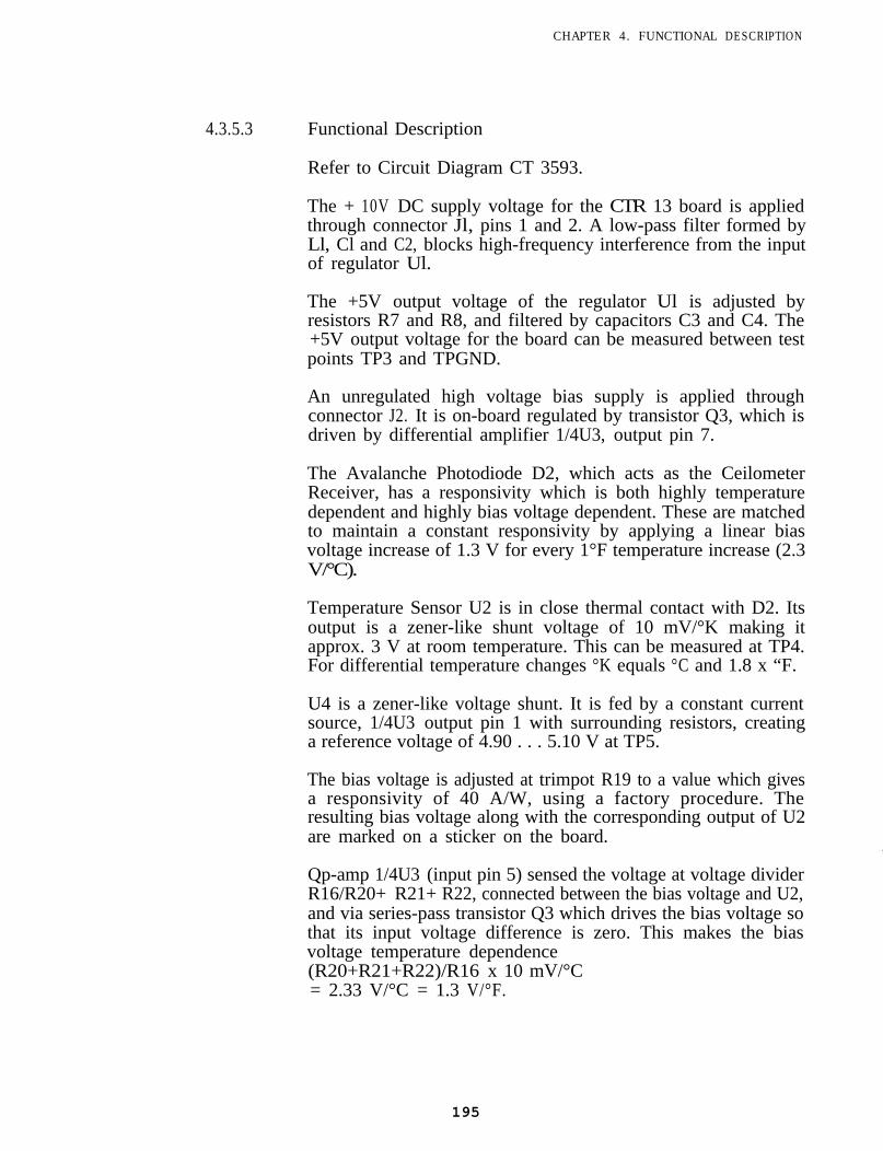
CHAPTER 4. FUNCTIONAL DESCRIPTION
4.3.5.3 Functional Description
Refer to Circuit Diagram CT 3593.
The + 10V DC supply voltage for the CTR 13 board is appliedthrough connector Jl, pins 1 and 2. A low-pass filter formed byLl, Cl and C2, blocks high-frequency interference from the inputof regulator Ul.
The +5V output voltage of the regulator Ul is adjusted byresistors R7 and R8, and filtered by capacitors C3 and C4. The+5V output voltage for the board can be measured between testpoints TP3 and TPGND.
An unregulated high voltage bias supply is applied throughconnector J2. It is on-board regulated by transistor Q3, which isdriven by differential amplifier 1/4U3, output pin 7.
The Avalanche Photodiode D2, which acts as the CeilometerReceiver, has a responsivity which is both highly temperaturedependent and highly bias voltage dependent. These are matchedto maintain a constant responsivity by applying a linear biasvoltage increase of 1.3 V for every 1°F temperature increase (2.3V/°C).
Temperature Sensor U2 is in close thermal contact with D2. Itsoutput is a zener-like shunt voltage of 10 mV/°K making itapprox. 3 V at room temperature. This can be measured at TP4.For differential temperature changes °K equals °C and 1.8 x “F.
U4 is a zener-like voltage shunt. It is fed by a constant currentsource, 1/4U3 output pin 1 with surrounding resistors, creatinga reference voltage of 4.90 . . . 5.10 V at TP5.
The bias voltage is adjusted at trimpot R19 to a value which givesa responsivity of 40 A/W, using a factory procedure. Theresulting bias voltage along with the corresponding output of U2are marked on a sticker on the board.
Qp-amp 1/4U3 (input pin 5) sensed the voltage at voltage dividerR16/R20+ R21+ R22, connected between the bias voltage and U2,and via series-pass transistor Q3 which drives the bias voltage sothat its input voltage difference is zero. This makes the biasvoltage temperature dependence(R20+R21+R22)/R16 x 10 mV/°C= 2.33 V/°C = 1.3 V/°F.
195
CHAPTER 4 . FUNCTIONAL DESCRIPTION
The negative input at J2, pin 3, is connected through currentmeasuring resistor R4 to the photodiode circuit forrned by D1,R5, R12 and the photodiode D2 itself. The photodiodeDC-current can be measured as a voltage drop across R4 betweentest points TP1 and TP2.
Resistor R5 serves for current limiting. Capacitor C9 restores alow impedance level and filters interference.
Photodiode D2 transforms the light power incident upon it intoa DC current proportional to the light power. Rapid currentchanges pass capacitor C8 to common-emitter preamplifier stageQl and emitter-follower stage Q2. Ql and Q2 drive feedbackresistor Rll and a voltage is produced (12.lk times Ql baseinput current).
Output is through capacitors C6 and C7 which block the DC-component. The output signal from connector J3 is connectedto the amplifier of Processor Board Al.
Resistors Rl, R2, and R3, divide the bias voltage by one-hundred,which is then brought to connector Jl. This is further routed tothe analog monitoring section of the Processor Board. Softwarereference is MRHV.
WARNING! Bias Voltage may reach 425V.
196
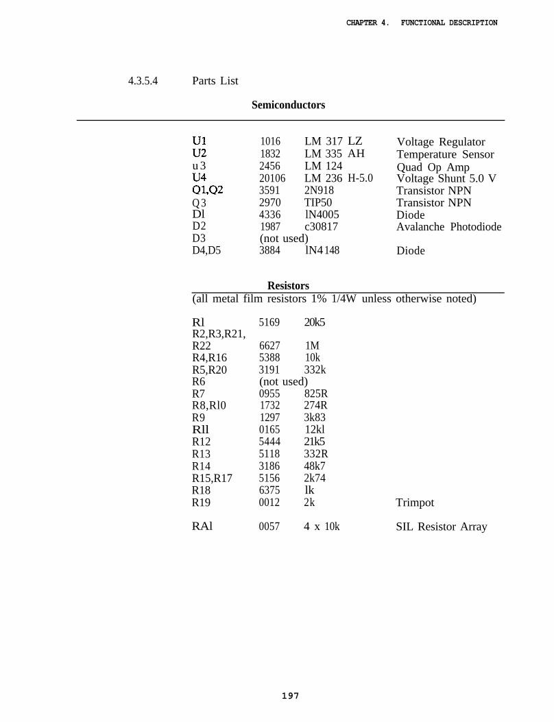
CHAPTER 4. FUNCTIONAL DESCRIPTION
4.3.5.4 Parts List
Semiconductors
;::u 3
:;ozQ 3DlD2D3D4,D5
1016 LM 317 LZ1832 LM 335 AH2456 LM 12420106 LM 236 H-5.03591 2N9182970 TIP504336 lN40051987 c30817(not used)3884 lN4 148
Voltage RegulatorTemperature SensorQuad Op AmpVoltage Shunt 5.0 VTransistor NPNTransistor NPNDiodeAvalanche Photodiode
Diode
Resistors(all metal film resistors 1% 1/4W unless otherwise noted)
Rl 5169 20k5R2,R3,R21,R22 6627 1MR4,R16 5388 10kR5,R20 3191 332kR6 (not used)R7 0955 825RR8,Rl0 1732 274RR9 1297 3k83Rll 0165 12klR12 5444 21k5R13 5118 332RR14 3186 48k7R15,R17 5156 2k74R18 6375 lkR19 0012 2k
RAl 0057 4 x 10k SIL Resistor Array
Trimpot
197
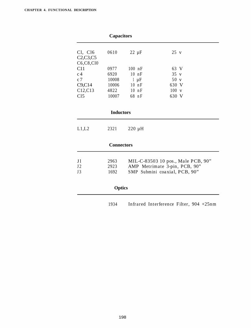
CHAPTER 4. FUNCTIONAL DESCRIPTION
Capacitors
Cl, Cl6 0610 22 µF 25 vC2,C3,C5C6,C8,Cl0C11 0977 100 nF 63 Vc 4 6920 10 nF 35 vc 7 10008 1 µF 50 vC9,C14 10006 10 nF 630 VC12,C13 4822 10 nF 100 vCl5 10007 68 nF 630 V
Inductors
L1,L2 2321 220 µH
Connectors
Jl 2963J2 2923J3 1692
MIL-C-83503 10 pos., Male PCB, 90”AMP Metrimate 3-pin, PCB, 90”SMP Submini coaxial, PCB, 90”
Optics
1934 Infrared Interference Filter, 904 +25nm
198
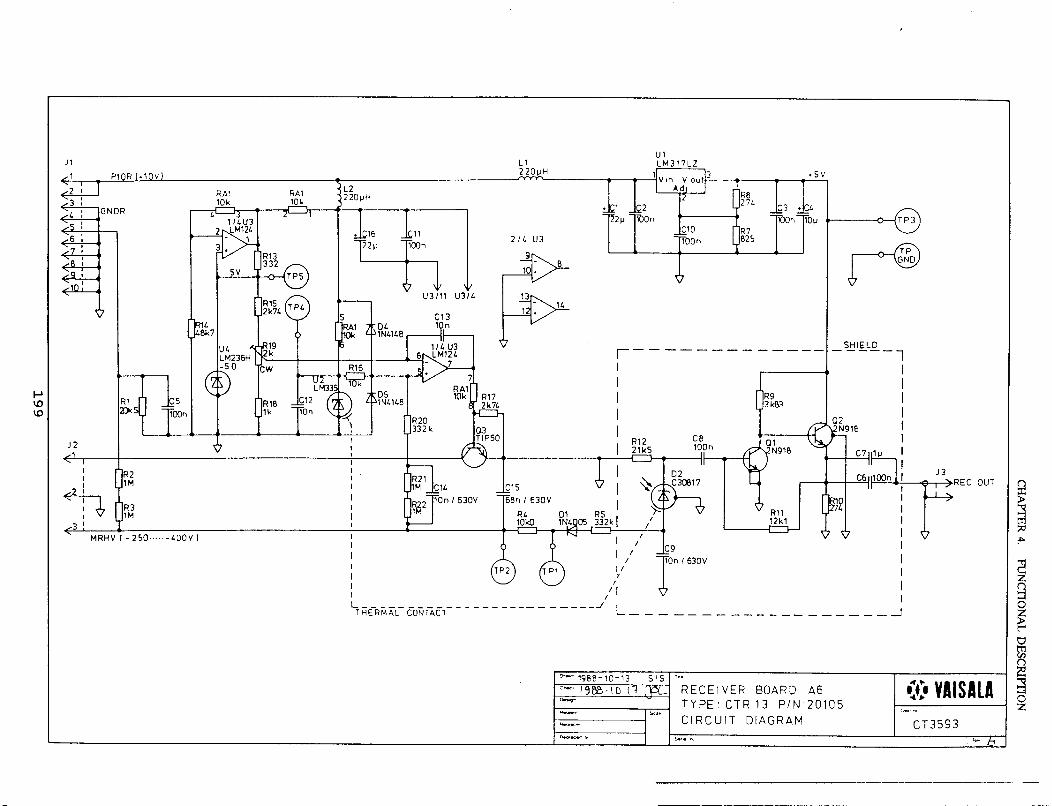
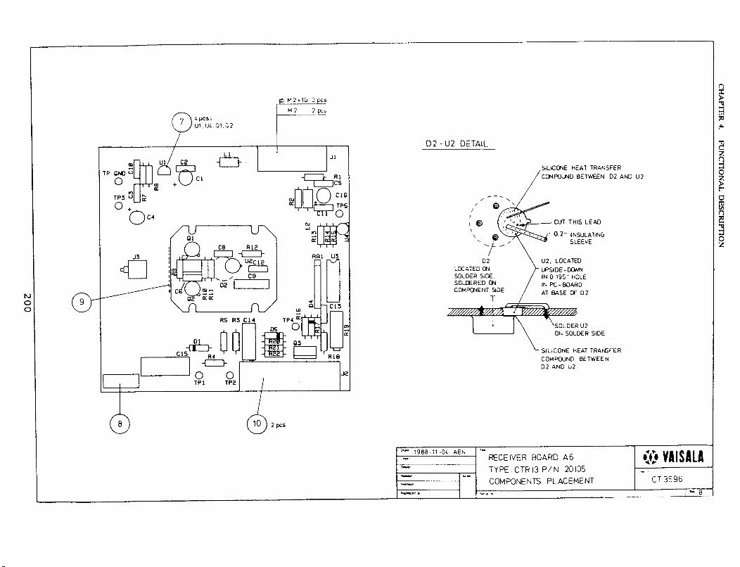
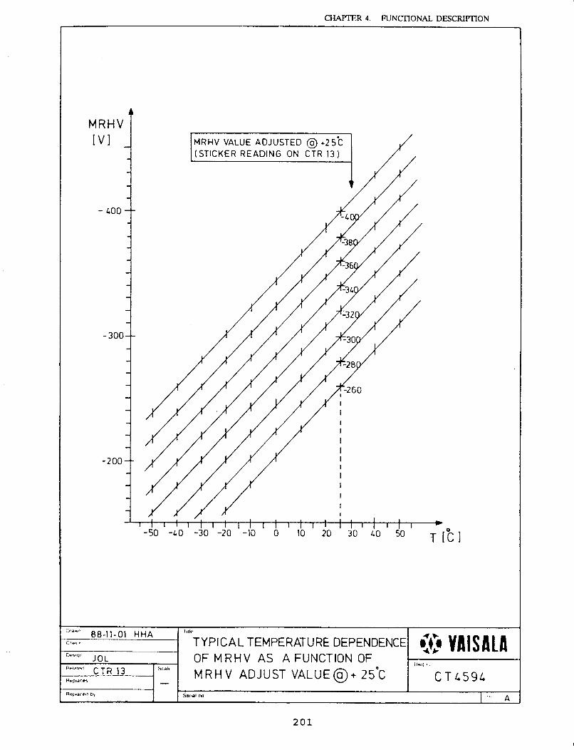
CHAPTER 4. FUNCTIONAL DESCRIPTION
4.3.6 Laser Transmitter Board CTT 12 REF A7
4.3.6.1 Introduction
The Ceilometer CT 12K uses laser light pulses to obtainreflections from any particles in the path of the collimated laserlight beam.
The Gallium Arsenide laser diode on the Transmitter board emitsthe laser light pulses under control of the processor board’s “LaserTrigger” signal.
The operating voltage for the laser diode is supplied by theon-board high-voltage regulator and is switched to the laser diodethrough the laser diode supply circuits by the triggering circuitry.
The laser diode operating voltage and temperature monitoringsignals are available for the processor and referred to as TL+,TL-(Laser Temperature) and PXHV (Positive Transmitter HighVoltage).
The board requires two voltage supplies: + 10V DC for thetriggering circuitry, and +260V DC for the high-voltage regulator.
The “Laser Trigger” signal activates triggering circuits to “switchon” the laser emission, providing one laser light pulse to traverseupward via the transmitter optics to the atmosphere.
The “Laser Trigger” signal is an active high and trailing edgesensitive pulse referred to as LTRG (Laser Trigger).
The positioning of the laser diode and its mounting hardware onthe transmitter board is extremely critical and is held to tightmanufacturing tolerances. This assures interchangeability of alltransmitter boards without the requirement of optical realignments.
4.3.6.2 Specifications
Type: Transmitter board CTT 12Part Number: 2687Designation: A7Supply Voltage: 260V DC ± 15%, 25mA
10V DC ± 15%, 20mADimensions: W x D x H
5.1 x 5.1 x 1.8 inches130 x 130 x 45 millimeters
202
CHAPTER 4. FUNCTIONAL DESCRIPTION
Laser Diode: LDL LD 224-8S
Monitored PXHV 1% of Laser Supply VoltageSignals: TL Laser Temperature
Trigger Pulse: 50 ns(LTRG)
Laser Pulse: Peak Power 40 WDuration, 50 % level 135 ns (typical)Energy (Dia. = 118nm) 6.6 µWsMax. repetition rate 1120 Hz
4.3.6.3 Functional Description
Refer to Circuit Diagram CT 3120.
The CTT 12 Transmitter Board consists of the following circuits:
- High-Voltage Regulator- Laser Diode Pulse Circuitry- Laser Diode- Laser Diode Triggering Circuitry
4.3.6.3.1 High-Voltage Regulator
The supply voltage of +260V DC is applied via connector J3, pin1, from Power Supply CTP 12 (Ref. PSl). It can be measuredbetween TP7 and GND.
The output current of the regulator is limited to 10mA and theoutput voltage is monitored via J2, pin 8, signal PXHV. Thevalue of PXHV is determined by resistors R12 and R13, whichdivides the output voltage of the laser diode regulator.
The high-voltage regulator consists of the following subcircuits:
- Control Stage- Error Amplifier
203
CHAPTER 4. FUNCTIONAL DESCRIPTION
Control Stage
The output is regulated with Darlington-connected transistors Q8and Q9.
The base voltage of transistor Q8 controls the output current ofthe regulator through transistor Q8 and Q9.
The output sink current of the error amplifier transistor Q7determines the voltage drop over resistor R24 and, therefore, thebase voltage of Q8. Zener diodes D8 and D9 limit its maximumvalue to 200V.
The regulator output current is limited to approximately l0mA.It is measured as a voltage drop over resistor R25. When thevoltage between the base of Q8 and the output exceeds theforward bias of diodes Dll, D12, and D13, these will conduct andlimit the base drive of Q8.
Error Amplifier
The differential error amplifier formed by transistors Q6 and Q7measures the output voltage; then, through resistors, scales thefeedback signal. The output voltage is adjusted with trimpot R21,changing the scale ratio of the feedback resistors for the erroramplifier.
The base of Q6 is connected to reference voltage of D7 (+ 12V)via scaling network of resistors R16, R17, and R18. R17 is anNTC-type resistor sensing the operating temperature of the laserdiode. Therefore, the scaling of the network (i.e., the basevoltage of Q6) changes according to the sensed temperature.Refer to Figure 1.
When the reference voltage value of the error amplifier increasesat the base of Q6, the output voltage of the regulator is increased.This temperature compensation is needed due to the operationalcharacteristics of the laser diode.
The error (amplifier) adjusts the output voltage to such a valuethat the feedback voltage at the base of Q7 equals the referencevoltage at the base of Q6. The Q7 collector current via R24adjusts the base voltage of the control stage transistor Q8 and,therefore, the output voltage.
204
CHAPTER 4. FUNCTIONAL DESCRIPTION
4.3.6.3.2 Laser Diode Pulse Circuit
Thyristors Q4 and Q5 are normally in a non-conducting statewhich allows the voltage regulator to charge the pulse energycapacitors C9, C12, and C14, to the regulated voltage. ResistorsR10 and Rll assure that the voltage is divided evenly over thethyristors.
When the ultrafast thyristors Q4 and Q5 are triggered throughtransformer Tl, capacitors C9, C12, and C14, are dischargedthrough the laser diode D6 in less than 200ns, peak current beingin the order of 50A. This will cause D6 to lase.PC-board-implemented inductor Ll limits the peak current andshapes the pulse. Ll also causes the capacitors to be dischargedto a slightly negative voltage which assures the “turn-off’ ofthyristors Q4 and Q5.
Diode D5 prevents the laser from being reverse-biased. Thecharge-discharge cycle can be measured at TP3. See Dwg 4417.
WARNING! Voltage in excess of I00V at TP3.
205
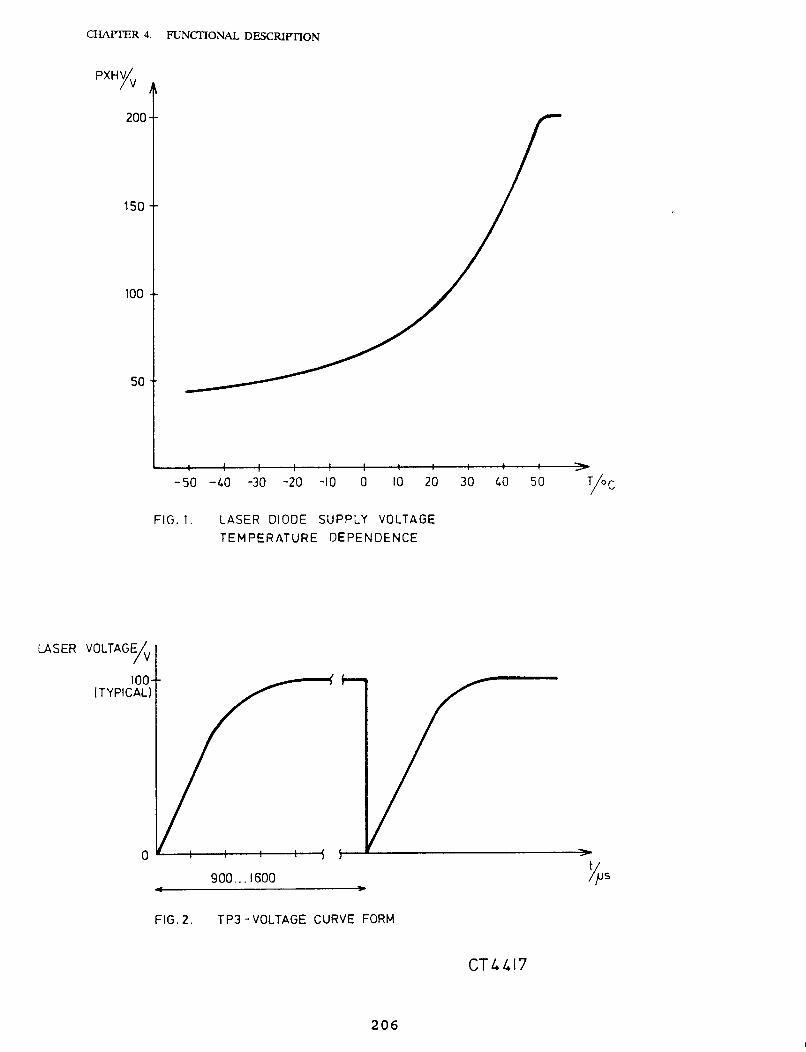
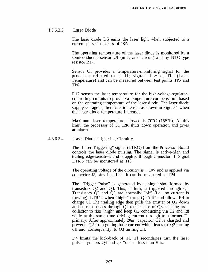
CHAPTER 4. FUNCTIONAL DESCRIPTION
4.3.6.3.3 Laser Diode
The laser diode D6 emits the laser light when subjected to acurrent pulse in excess of 18A.
The operating temperature of the laser diode is monitored by asemiconductor sensor Ul (integrated circuit) and by NTC-typeresistor R17.
Sensor Ul provides a temperature-monitoring signal for theprocessor referred to as TL; signals TL+ or TL- (LaserTemperature) and can be measured between test points TP5 andTP6.
R17 senses the laser temperature for the high-voltage-regulator-controlling circuits to provide a temperature compensation basedon the operating temperature of the laser diode. The laser diodesupply voltage is, therefore, increased as shown in Figure 1 whenthe laser diode temperature increases.
Maximum laser temperature allowed is 70°C (158°F). At thislimit, the processor of CT 12K shuts down operation and givesan alarm.
4.3.6.3.4 Laser Diode Triggering Circuitry
The ‘Laser Triggering” signal (LTRG) from the Processor Boardcontrols the laser diode pulsing. The signal is active-high andtrailing edge-sensitive, and is applied through connector Jl. SignalLTRG can be monitored at TPl.
The operating voltage of the circuitry is + 10V and is applied viaconnector J2, pins 1 and 2. It can be measured at TP4.
The ‘Trigger Pulse” is generated by a single-shot formed bytransistors Q2 and Q3. This, in turn, is triggered through Ql.Transistors Q2 and Q3 are normally “off’ (i.e., no current isflowing). LTRG, when “high,” turns Ql “off’ and allows R4 tocharge Cl. The trailing edge then pulls the emitter of Q2 downand current passes through Q2 to the base of Q3, causing itscollector to rise “high” and keep Q2 conducting via C2 and R8while at the same time driving current through transformer Tlprimary. After approximately 20ns, capacitor C2 is charged andprevents Q2 from getting base current which leads to Q2 turningoff and, consequently, to Q3 turning off.
D4 limits the kick-back of Tl. Tl secondaries turn the laserpulse thyristors Q4 and Q5 “on” in less than 20ns .
207
CHAPTER 4. FUNCTIONAL DESCRIPTION
4.3.6.4 Parts List
Semiconductors
Q1,Q3
Q2
0285 1832
5416Q4,Q5 2369Q6-Q9 2970D l-D5, 3384Dl0-D13D6 1960
D7 4011D8,D9 2972
LM335H2N29072N2222GA201TIP50lN4148
LD224-8S
lN759lN985
Temperature SensorTransistor PNPTransistor NPNThyristorTransistor NPNDiode
Laser Diode
Zener Diode 12VZener Diode 100V
Resistors(all metal film resistors l%, 0.25W)
(unless otherwise stated)
Rl,R2,R6 6355R8,R28R3 5116R4 5453R5 6373R7 6375R9 3163Rl0,Rll,R13 1188R12,R22 3176R4,R15,R24 4080R16,R23 5467R17 2490R18 5444R19 5791R20 4247R21 7464R25 5699R26 4242R27,R29 5388
215R
48R7487R100Rlk010R0562k5k62220k33k233k21k53k32150k10k38R31k010k0
Carbon Film, 5%, 0.5W
NTC
Carbon Film, 5%, 0.5WTrimpot, 15-turns, 3/4W
Carbon Film 5%, 0.5W
208
Hugh Black
Hugh Black
Hugh Black
U1
CHAPTER 4. FUNCTIONAL DESCRIPTION
Capacitors
C l 4782 220pF 100VC2 5734 100pF 63V
C4,C5,C84802 1nF 100V
C9,C12,C14 4507 100nF 63V22µF 400V
C6 10007 68nF 630VC7 10008 1µF 50V
Inductors
Ll Part of PC-Board Layout
Tl FACTORY-ASSEMBLED FromP/N 1863
Miscellaneous
1863 Toriod dia. l0mm, Ref.Tl Assembly
Connectors
Jl 1692
J2 2963
J3 2923
SMB-Submini CoaxialPCB 90°
MILC-83503,10 Male,posPCB 90°
AMP 207541-3,3 Male,posPCB 90°
209
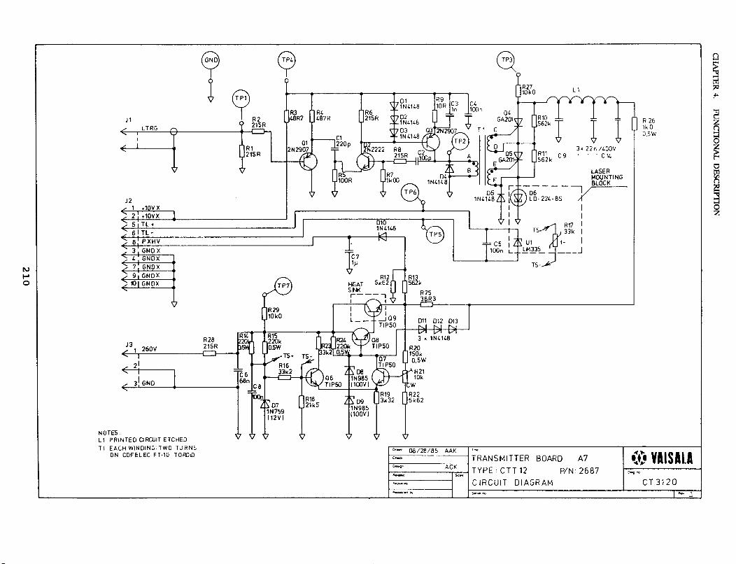
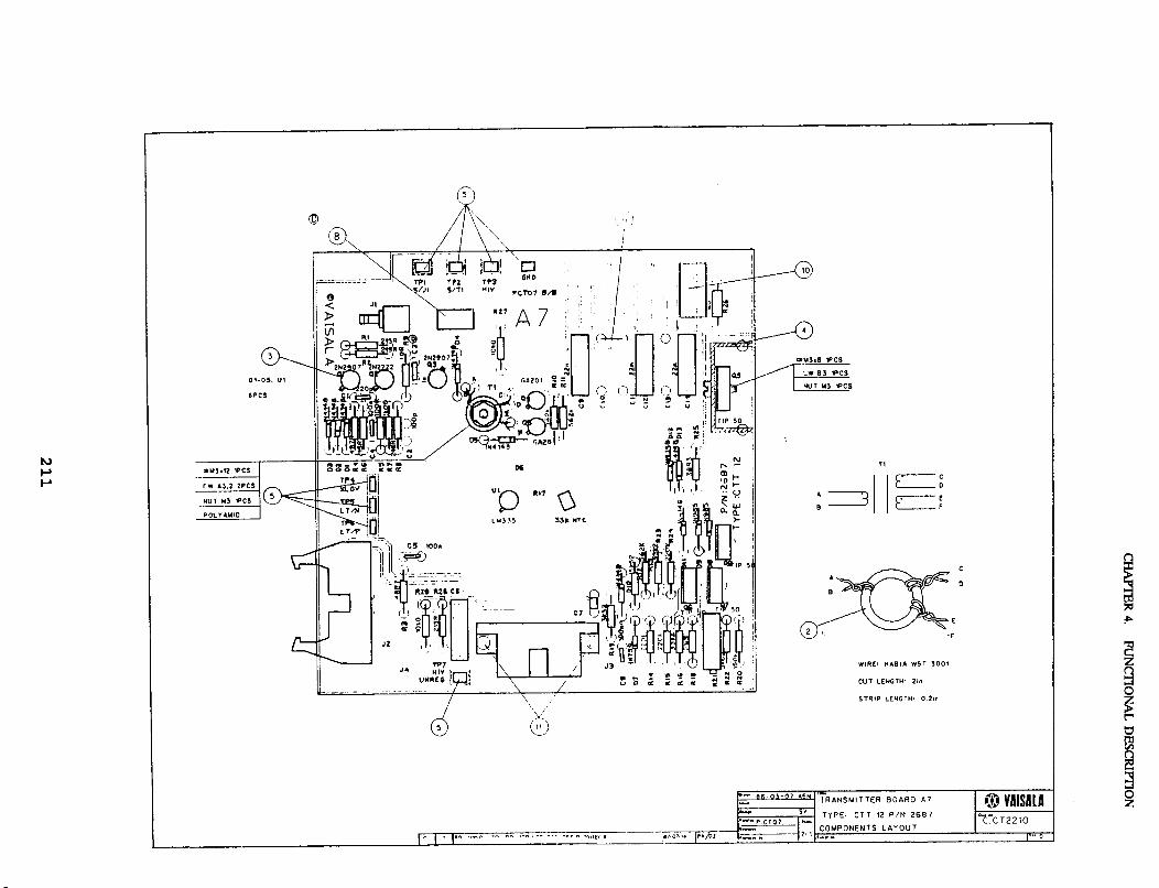

212

CHAPTER 4. FUNCTIONAL DESCRIPTION
4.3.7 High-Voltage Power Supply CTP 12 REF PSl
4.3.7.1 Introduction
The High-Voltage Power Supply CTP 12 is the 115V Line InputVoltage subunit of the Ceilometer CT 12K. It performs thefollowing main functions:
- Transforms the line voltage to the low voltages needed by theelectronics.
- Transforms the line voltage, and also rectifies, filters, andpartly regulates, the high voltages needed by the transmitterlaser diode and the receiver avalanche photodiode.
- Switches the line voltage by power relays to control theCeilometer Window Conditioner.
4.3.7.2 Specifications
Type: CTP 12Part Number: 2688ReferenceDesignation; PSlDimensions: W x D x
7.1 x 11.8 xH5.8 in
180 x 300 x 148 mm
Weight: 10.1 lbs4.6 kgs
Line Input: 102V min. - 132V max.45Hz - 65Hz12A max. continuous
213
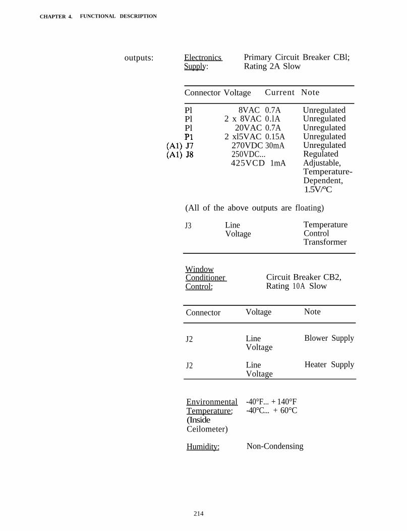
CHAPTER 4. FUNCTIONAL DESCRIPTION
outputs: Electronics Primary Circuit Breaker CBl;Supply: Rating 2A Slow
Connector Voltage Current Note
PlPlPl
8VAC 0.7A2 x 8VAC 0.lA
20VAC 0.7A2 xl5VAC 0.15A
270VDC 30mA250VDC...425VCD 1mA
UnregulatedUnregulatedUnregulatedUnregulatedUnregulatedRegulatedAdjustable,Temperature-Dependent,1.5V/°C
(All of the above outputs are floating)
J3 LineVoltage
TemperatureControlTransformer
WindowConditionerControl:
Circuit Breaker CB2,Rating 10A Slow
Connector Voltage Note
J2 LineVoltage
Blower Supply
J2 LineVoltage
Heater Supply
Environmental -40°F... + 140°FTemperature: -40°C... + 60°C(InsideCeilometer)
Humidity: Non-Condensing
214
CHAPTER 4. FUNCTIONAL DESCRIPTION
4.3.7.3 Functional Description
Refer to Circuit Diagram CT 3289.
4.3.7.3.1 General
The Line Supply is brought in via connector Jl to Terminal BlockJ5 and, further, to Indicator Lamp DSl and Circuit Breakers CB1and CB2. DSl is placed before the CB’s to indicate whetherpower is applied regardless of the state of the breakers.
Circuit Breakers CBl and CB2 double as “ON/OFF” switches andcircuit protectors. The dual pole configuration enables the useof a floating or non-specified line supply. CBl supplies theCeilometer equipment and connects power to Terminal Block J5where the over-voltage protectors Rl, R2, and R3, are located(i.e., Metal-Oxide Varistors). From J5, power is divided tointernal transformers Tl and T2, and via J3, to the externalTemperature Control Transformer. In 115V operation of alltransformer primaries are connected in parallel.
4.3.7.3.2 Window Conditioner Control
Circuit Breaker CB2 supplies line power to the contacts of relaysKl and K2, and from these to the output connector J2, Kl andK2 are controlled by signals BLOWER ON (BON) and HEATERON (HON) from connector P2. Kl and K2 are active when BONand HON are at ground potential, respectively. The relaycontacts are so arranged that heating cannot be supplied unlessthe blower is ON.
The Window Conditioner-monitoring temperature sensor signalsTB+ and TB- are connected via PSl from connector J2 toconnector P2.
4.3.7.3.3 High-Voltage Outputs
The High-Voltage Transformer T2 secondaries are connected viafuses Fl and F2 to High-Voltage Power Supply Board PSl Al.Fuses Fl and F2 values shah be 60mA (1/16A) when using 0.25x 1.25-inch fuses, and 50mA when using 5 x 20-millimeter fuses.
One secondary supplies the Avalanche Photodiode Receiver biasvoltage regulating circuit while the other secondary isfullwave-rectified and filtered at J8, and connected to theTransmitter Board (A7) for onboard regulating.
215
CHAPTER 4. FUNCTIONAL DESCRIPTION
The operation of the receiver bias voltage-regulating circuit is asfollows:
The 200VAC from T2 is rectified, filtered, and doubled, in circuitDl-Cl-C2-D2 to 550VDC. This biases a l0mV/°K temperaturesensor Ul which, together with diode D3, creates a referencevoltage of approximately 2.5V at room temperature with atemperature coefficient of 12mV/°K (22mV/°F) between diodesD3 and D4. D4 serves for temperature compensation of thetransistor Q5 base-emitter voltage drop.
The output voltage is sensed with adjustable voltage divider R14-R12-R13-R15 and connected via Q5 to a difference amplifierQ3-A4 where the difference between reference and output controlsthe base of series-pass transistor Q2. The drive is supplied byR8-R9. Transistor Ql takes half of the regulation voltage dropwhich, in case of output short-circuit, may exceed that of a singleseries-pass transistor.
Current limiting is achieved when the voltage over R16 exceedsthat of a diode junction (i.e., approximately 0.6V). The maximumoutput current with full voltage is approximately 1mA. When thisoccurs, diodes D6 and D7 will conduct excess Q2 base drivecurrent to the output.
Zeners D8, D9, and Dl0, l imit the output voltage toapproximately 450V max while Zener D5 provides a collectorvoltage drop for Q4 and Q5 to within specifications of theirbreakdown voltage.
Resistors R17 and R18 provide protection for test points TPl andTP2.
Additional filtering is provided by C4,C5, and C6, and the finaloutput voltage is from connector J7 to Receiver Board A6.
The actual bias voltage for the Receiver Photodiode is adjustedby R13. The voltage to be achieved at room temperature (22°Cor 72°F) is found on a sticker mounted on the Receiver Board.For other temperatures, the adjustment value shall be correctedby applying the output voltage temperature coefficient 1.5V/°Cor 2.7V/°F.
If the Ceilometer is equipped with Receiver board CTR 13, whichhas it’s own bias voltage compensation circuit, R13 has to beadjusted to it’s maximum (fully clockwise).
216
CHAPTER 4. FUNCTIONAL DESCRIPTION
4.3.7.4 Parts List
PartReference Number Description
CBl 2956
CB2 2958
Kl,K2 10021
32 2952
33 2954
Fl,F2 10179
Circuit Breaker2A Slow Airpax T21-2-2.0-01-00Circuit Breaker10A Slow Airpax T21-2-10.0-01-00Relay 24VDC/DPDT 16ASigma 68R24-24DC-SCOFuseholderLittlefuse 345603-010Fuse Knob - 0.25 x 1.25 inchLittlefuse 345603-020Fuse 62mA Slow - 0.25 x 1.25 inch
10 10011
DSl 10231
Rl 0956
R2,R3 10002
TerminalWeidmuller AKZ 4SS PAIndicator Lamp - 125V, 00.5-inch1D1 1030 DlMetal Oxide Varistor - 275V, 15AGE V275 LA 15Metal Oxide Varistor - 150V, 10AGE V150 LA 10
10274 Main Transformer Subassembly
Tl
Pl
2722 TransformerVaisala CT 3113
2931 Header.18-pos. AMP 207442-l
2936 SocketAMP 163k084-2
10275 Line Input Harness Subassembly
Jl 2929 Receptacle6-pos., AMP 207153-l
2934 PinAMP 163082-2
217
CHAPTER 4. FUNCTIONAL DESCRIPTION
10276 Blower Control Harness Subassembly
P2
J2
2929
2928
2934
2936
Receptacle6-pos. AMP 207153-lHeader6-pos, AMP 207152-lPinAMP 163082-2SocketAMP 163084-2
10277 Temperature Control TransformerHarness Subassembly
J3
T2
2928
2936
2934
2723
Header6-pos, AMP 207152-lSocketAMP 163084-2PinAMP 163082-2Transformer Vaisala CT 3114
218
CHAPTER 4. FUNCTIONAL DESCRIPTION
Al 2715 High Voltage Power Supply Board
Ul 1832
Q l - Q 5 2970
D l,D2, 1336Dll-D14D3,D4,D6, 3 8 8 4D7D5 2972
D8,D9,Dl0 2971
R4,R5 4080
R6-R9 4248
R10 5791
Rll,R15 7481
R12,R14 4247
R13 0012
R16 5153
R17,R18 5388
Cl,C2,C7 10003
c3 4507
C4-C6,C8 10007
J7,J8 2924
Temperature SensorNS LM335Transistor NPN 400VTI TIP50Diode 600V 1AlN4005Diode 75V 0.2AlN4148Zener 1OOV 0.4WlN985Zener 150V 0.4WlN989Resistor Carbon Film220k 5% 0.5WResistor Carbon Film330k 5% 0.5WResistor Metal Film3k32 1% 0.25WResistor Metal Filmlk47 1% 0.25WResistor Carbon Film150k 5% 0.5WTrimpot2k 0.75W, 15 TurnsResistor Metal Film681R 1% 0.25WResistor Metal Film10k 1% 0.25WCapacitor Alum El22µ 350v
Capacitor Ceramicloon 63VCapacitor Polyest68n 630VConnector3-pos. AMP 207608-3
219
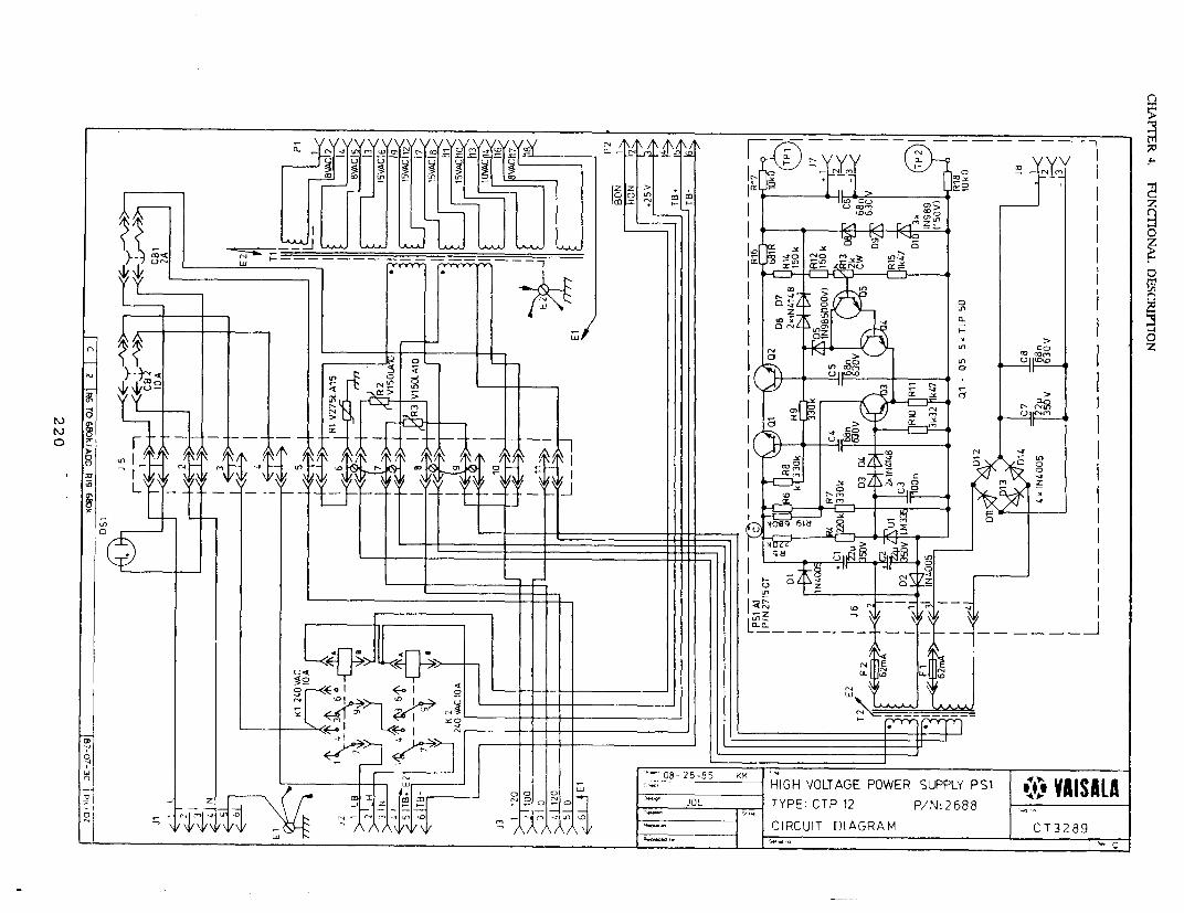
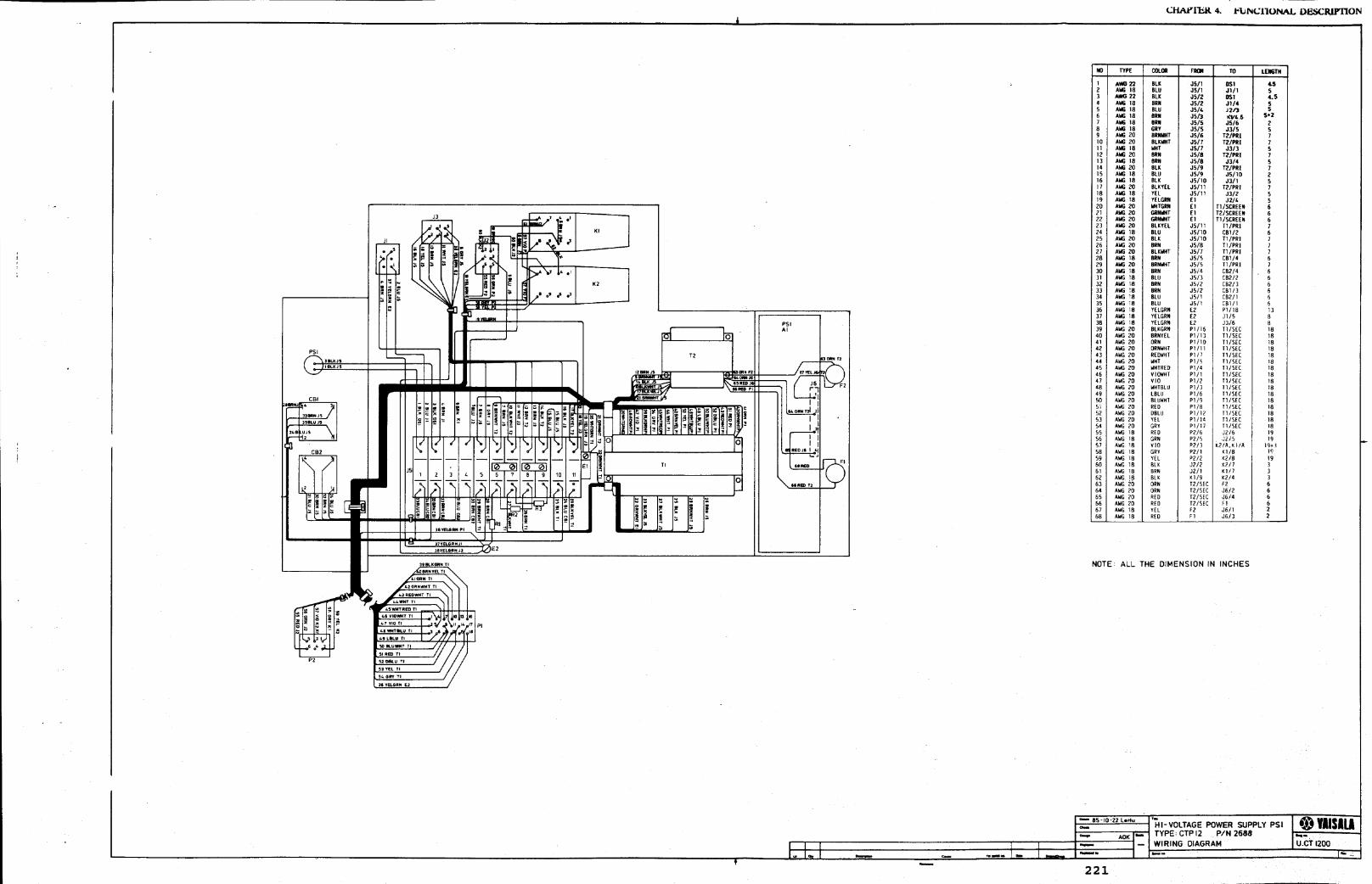
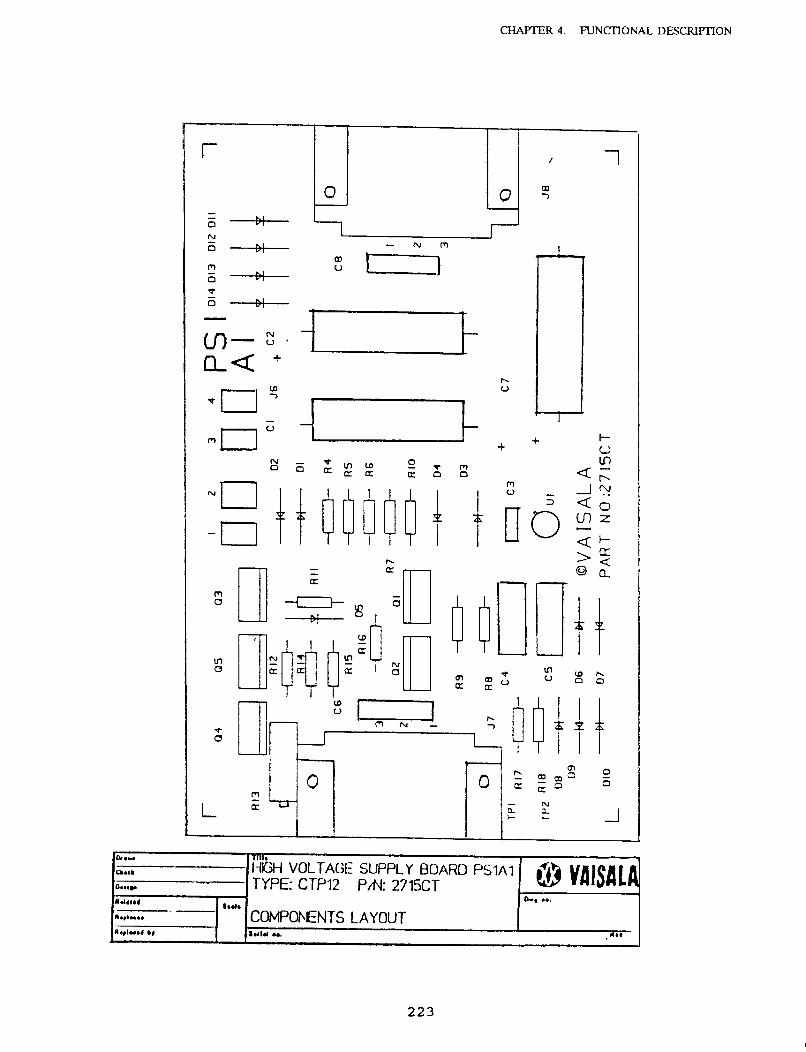

224
CHAPTER 4. FUNCTIONAL DESCRIPTION
4.3.8
4.3.8.1
Window Conditioner Bl
Introduction
The Window Conditioner of the CT 12K Ceilometer serves forkeeping the windows on top of the instrument free fromprecipitation and dust. In addition, it is used for regulating thetemperature of the Ceilometer. It is controlled by the processorof the Ceilometer via two power relays in the High-Voltage PowerSupply PS 1.
4.3.8.2 Specifications
Part Number:2736Designation: B 1Dimensions: W
22.8 xD16.5 x
H13.4 inches
580 x 420 x 340 millimeters
Weight: 21 lbs9.5 kg
Blower Fan: Single-Phase 1 15VAC, 75W,Capacitor Coupled
Air Volume: 410m³/h14450ft³/h
BallBearings: Maintenance-Free
LifeExpectancy: 4.5 Years at 20°C (68°F)
in ContinuousOperation
Heater: Silicon Insulated FoilPower 600W NominalResistance 44 ohm + 44 ohm,Parallel-Connected at 115V
Safety Open at 256°F (124°C), IncreasingThermostat: Close at 202°F (94°C), Decreasing
Rating: 100,000 Cyclesat ll5VAC, 15A
Temperature Semiconductor-Type,Sensor: Voltage Drop 10mV x T/°K
Air SpeedOver Window Pane: 33ft/s (l0m/s)
Air Temperature Rise: 13°F (7°C) Typical
225
CHAPTER 4. FUNCTIONAL DESCRIPTION
4.3.8.3 Functional Description
Reference Circuit Diagram
Window Conditioner Bl . . . . . . . . . . . . CT 4290
Processor Board Al . . . . . . . . . . . . . . . CT 3386 (2/4)
Unregulated Power Supply Board A2 . . . CT 3196
High-Voltage Power Supply PSl . . . . . . . CT 3289
Ceilometer Wiring Diagram . . . . . . . . . CT 1104
The Processor Board Al outputs, HON and BON, are routed viaUnregulated Power Supply Board A2 to its connector, Jll, wherethey connect to High-Voltage Power Supply PSl and drive relaysKl and K2.
Line power is supplied via a dedicated circuit breaker, CB2 inPSl, to relays Kl and K2 contacts. These are connected so thatheating is not possible unless the blower is on. The Line Supplysignals, LB (Blower) and LH (Heater), are then routed from PSlthrough harness W2 and Ceilometer connector J2 to the WindowConditioner.
Heating Resistor HRl foils are parallel-connected for 115Voperation. Its heat is transferred to the Radiator (part 7) uponwhich the Safety Thermostate Sl and the temperature Sensor TS2are mounted.
The Blower housing is designed to create an even, efficientairflow over the radiator, picking up approximately 13°F of heatbefore sweeping over the windows of the Ceilometer.
Operation is monitored with Temperature Sensor TS2 which isconnected via PSl and A2 to Processor Board Al Monitor A/Dconverter channel 11 (software reference TB).
226
CHAPTER 4. FUNCTIONAL DESCRIPTION
Monitoring criteria are:
When both Heater and Blower are “ON,” the temperatureshall be less than 72°F (40°C) above ambient as measuredwith TSl (Ref. TE). If Blower only is “ON,” then thedifference limit is 54°F (30°C).
If heater has been ON (and subsequently the blower) for morethan 10 minutes, then TB shall exceed TE by 3°C or more.
If temperature TB exceeds external temperature TE by 72°F(40°C), more heating is cut off by software control and ahardware alarm is given.
The temperature measurement circuit is monitored against thealarm limit TB (ALIM TB; default value 176°F = 80°C) toinsure proper operation.
Four (4) minutes time-filtering is used.
As a final safeguard against overheating, the Safety ThermostatSl cuts off heating supply at 256°F ± 6°F (124°C ± 3°C).The processor gets no information of its operation, however.
The heat and the airflow are also used for stabilizing theimmediate environmental conditions of the Ceilometer. Incold weather, (T + 14°F = -10°C) the heating is always “ON”(together with blowing); and, in hot weather (T> + 86°F =+30°C), the blowing is always “ON” and heating “OFF’ tokeep heating by solar radiation at a minimum.
In intermediate temperatures, the o p e r a t i o n i ssoftware-controlled to keep both heating and blowing “ON”always when there are clouds being detected in low visibilityconditions; and, in 5 - minutete -inute periods every 60 minutes to insurerecovery in all situations and to keep dust contamination ata minimum.
227
Hugh Black
CHAPTER 4 . FUNCTIONAL DESCRIPTION
4.3.8.4 Parts List
Bl 10250Cl 10251HR1 2744TS2 2746Sl 2745E l 10011
Pl
1923
273 1100452944
Blower Motor and FanMotor CapacitorHeaterTemperature SensorThermostat SubassemblyTerminal,4-pin, 0.11 inchWire Terminal,0.11 inch in Female, AWG 18Connection Cable SubassemblyCable Alpha 45068Connector MS 3 116F16-8P
228
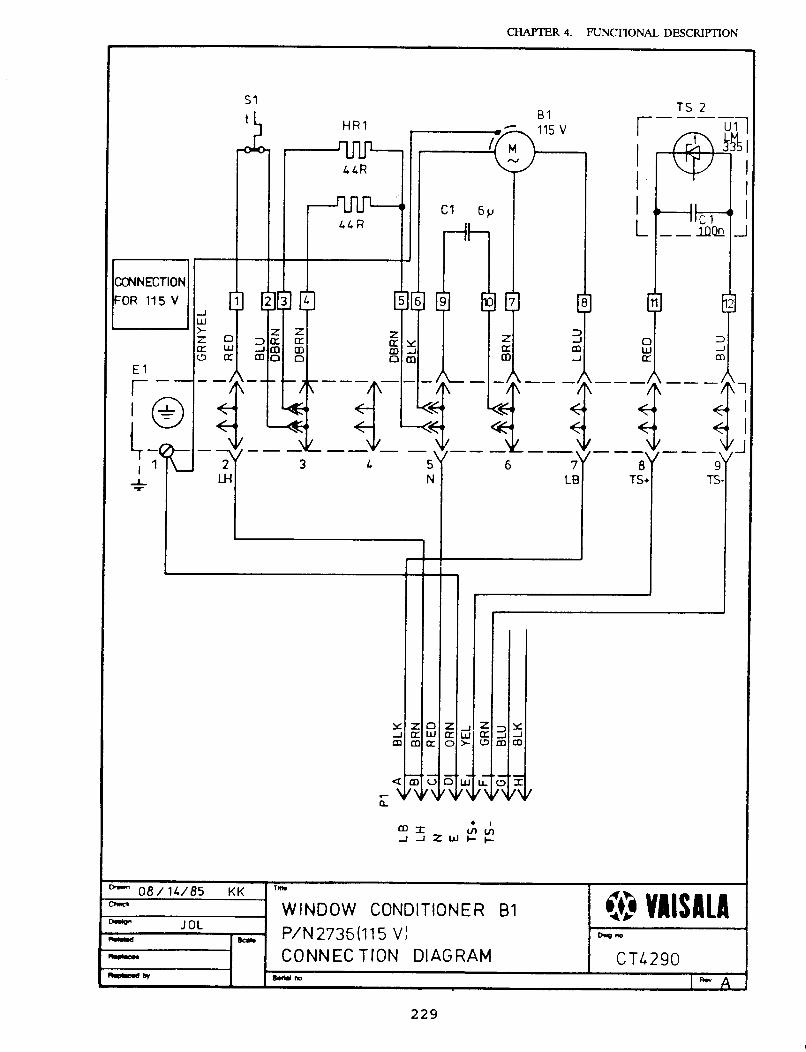
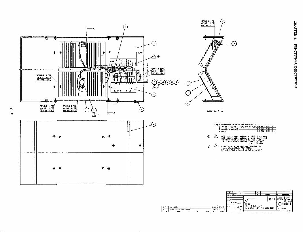
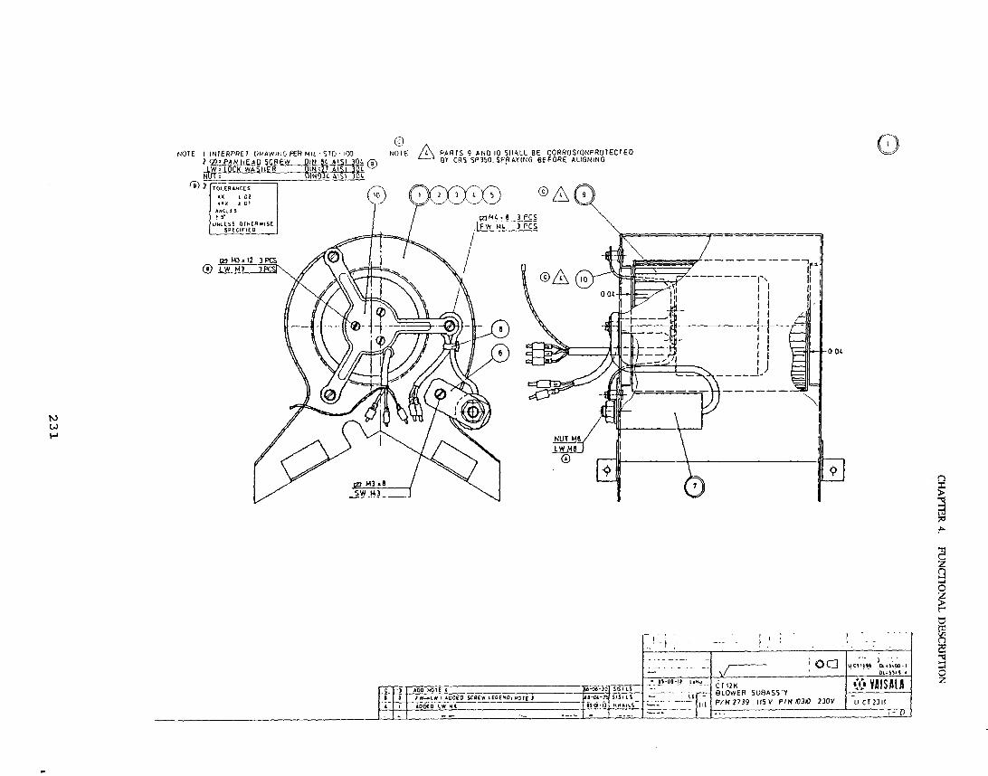
CHAPTER 4. FUNCTIONAL DESCRIPTION
4.3.9 Maintenance Terminal CTH 12
4.3.9.1 Introduction
Maintenance Terminal CTH 12 is designed for service andmaintenance of Ceilometer CT 12K.
It is a portable, near-pocket-size, hand-held terminal operatingover a wide temperature range. It is built into a plastic case, witha lid covering the display and the keyboard when not in use.
It operates with standard RS-232C signals. The operating power,+ 12V, is supplied from the Ceilometer.
The terminal contains a 16-character LCD display that supportsthe full ASCII character set. It also contains an electro-luminencelight for night readability and a heater element for lowtemperature operation, both controlled automatically by built-insensors.
The keyboard is a 16-character hexadecimal pad.
4.3.9.2 Specifications
Type: CTH 12Part Number: 2690Supply Voltage: 12V DC ±20%Current consumption: 50mA; with heater on: 25OmA
OperatingTemperature Range: -40°C... + 50°C
-40°F... + 120°F
MechanicalDimensions:
W x D x H5.0 x 7.7 x 2.0 inches127 x 196 x 5 1 millimeters
Cable: 1.2m4 ft
Interface:Baud Rate:Data Frame:(Standard)
RS-232C level RXD, TXD300 Baud (Standard)1 Start Bit8 Data Bits(Polarity of Unused 8th Bit (MSB)Same as Stop Bit)1 Stop BitNo Parity
232

CHAPTER 4. FUNCTIONAL DESCRIPTION
Display: 16-Character, Alphanumeric LCD,5 x 7 Dot Matrix
NightReadability: Electro-Luminence Light
Backlighting
Heating: Foil ResistorTemperature Sensor-ControlledHeating “ON” Temperature: -12°C (+ 10°F)Heating “OFF’ Temperature: -2°C ( + 28°F)
Heating Power: 2.5 W
Keyboard: 16-Key Hexadecimal KeyboardModule with Symbols 0...9 andA...F
233
CHAPTER 4. FUNCTIONAL DESCRIPTION
4.3.9.3 Functional Description
4.3.9.3.1 Operation
4.3.9.3.1.1 Keyboard
A 16-key, matrix-coded, hexadecimal keyboard is used with thekeys 0...9 and A...F as follows:
Column
H G F E
M 0 1 2 3
L 4 5 6 7Line
K 8 9 A B
J C D E F
The keyboard module is wired so that when a key is depressed,the key switch shorts a certain line to a certain column. Forexample, when the key “0” is pressed, line “M” connects to column“H.” Designations of the columns “H” to “E” and lines “M” to “J”refer to pin designations of keyboard module connector. Theconnector pins are arranged as follows (seen from the left to theright when viewing the keyboard from the normal operatingdirection): M L K J H G F E
4.3.9.3.1.2 Keyboard Control Circuit
Keyboard reading is controlled by a 16-key encoder (74C922)designated U9. The circuit is provided with internal pull-upresistors and a contact debounce circuit. The Data Ready (DA)signal goes “HIGH” when the key is pressed and returns "LOW"when the key is released. The speed of the scanning circuit isapproximately 600 Hz and the operating time of the debouncecircuit is about 10ms.
The circuit operates as follows:
The circuit clock feeds a two-bit counter which pulls down onecolumn, output Cl...C4, at a time through the decoder while theother column outputs are in high-impedance state. When no keyis being pressed, all line inputs are “ones” (l’s), this being affectedby the internal pull-up resistors.
234
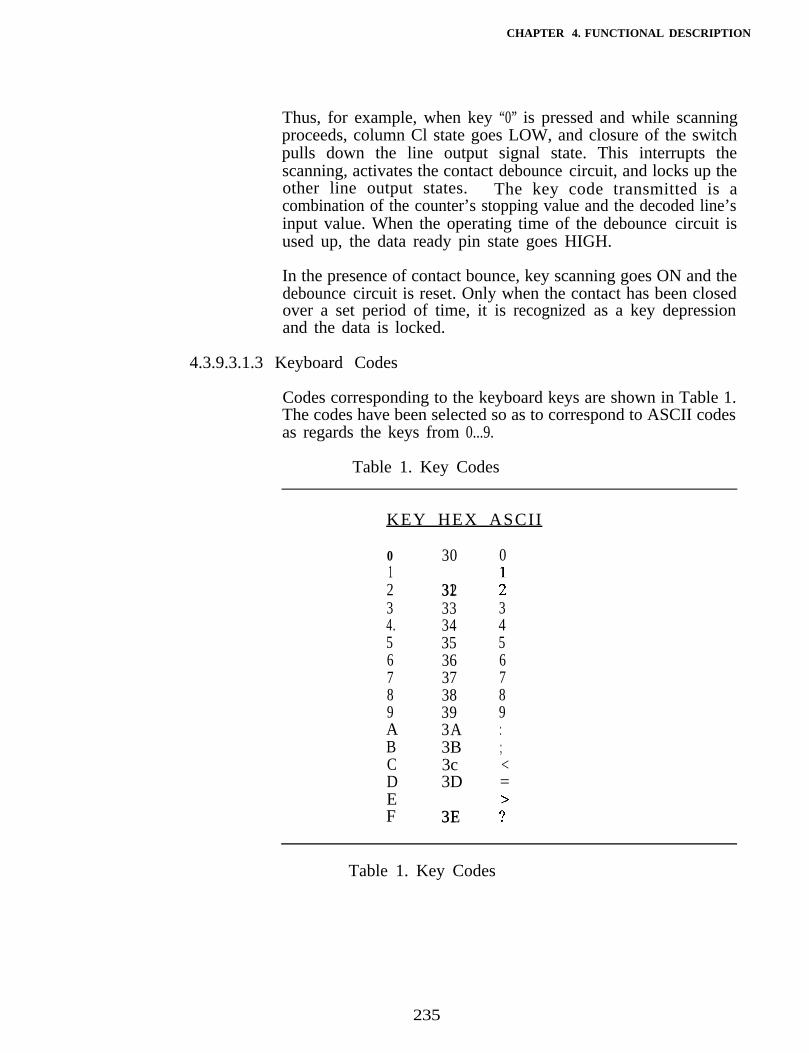
CHAPTER 4. FUNCTIONAL DESCRIPTION
Thus, for example, when key “0” is pressed and while scanningproceeds, column Cl state goes LOW, and closure of the switchpulls down the line output signal state. This interrupts thescanning, activates the contact debounce circuit, and locks up theother line output states. The key code transmitted is acombination of the counter’s stopping value and the decoded line’sinput value. When the operating time of the debounce circuit isused up, the data ready pin state goes HIGH.
In the presence of contact bounce, key scanning goes ON and thedebounce circuit is reset. Only when the contact has been closedover a set period of time, it is recognized as a key depressionand the data is locked.
4.3.9.3.1.3 Keyboard Codes
Codes corresponding to the keyboard keys are shown in Table 1.The codes have been selected so as to correspond to ASCII codesas regards the keys from 0...9.
Table 1. Key Codes
KEY HEX ASCII
01234.56789ABCDEF
30 0
3132 :.33 334 435 536 637 738 839 93A :3B ;3c <3D =
3E3F 7:
Table 1. Key Codes
235
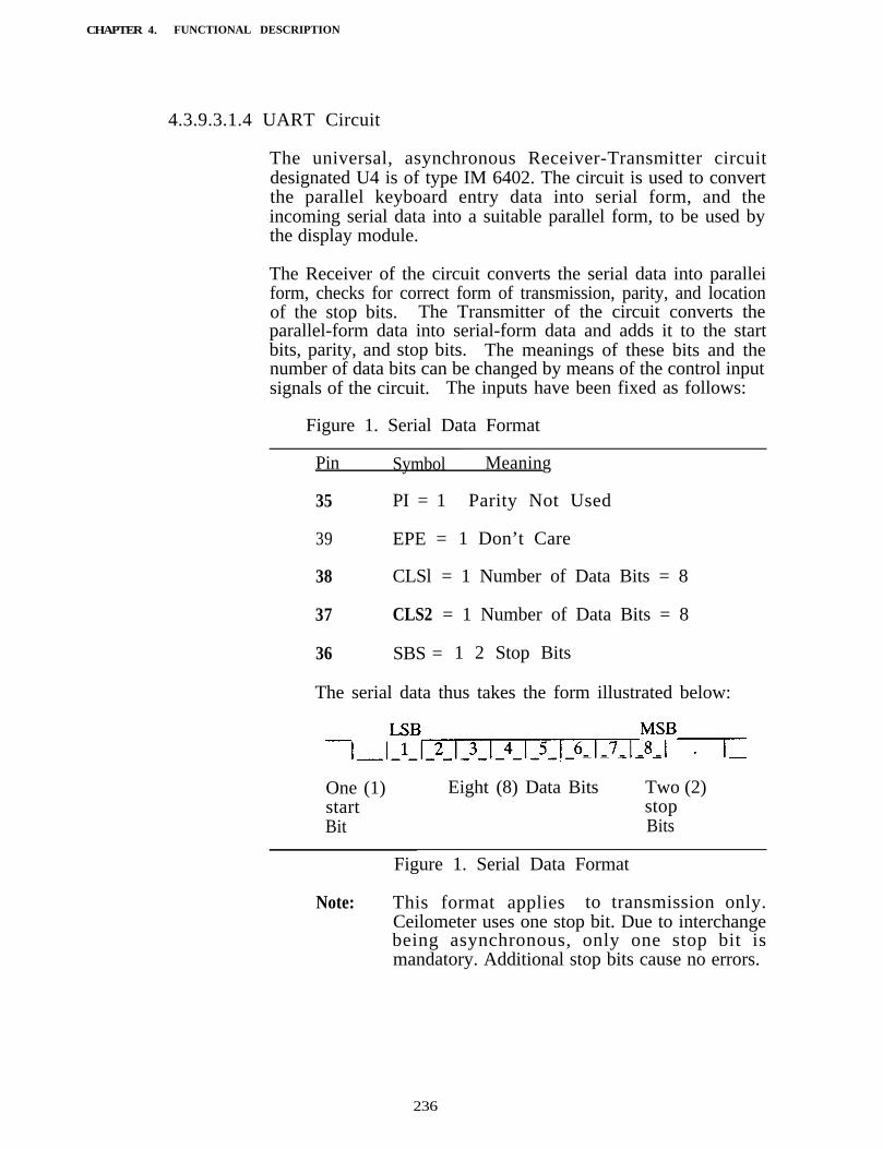
CHAPTER 4. FUNCTIONAL DESCRIPTION
4.3.9.3.1.4 UART Circuit
The universal, asynchronous Receiver-Transmitter circuitdesignated U4 is of type IM 6402. The circuit is used to convertthe parallel keyboard entry data into serial form, and theincoming serial data into a suitable parallel form, to be used bythe display module.
The Receiver of the circuit converts the serial data into paralleiform, checks for correct form of transmission, parity, and locationof the stop bits. The Transmitter of the circuit converts theparallel-form data into serial-form data and adds it to the startbits, parity, and stop bits. The meanings of these bits and thenumber of data bits can be changed by means of the control inputsignals of the circuit. The inputs have been fixed as follows:
Figure 1. Serial Data Format
Pin Symbol Meaning
35 PI = 1 Parity Not Used
39 EPE = 1 Don’t Care
38 CLSl = 1 Number of Data Bits = 8
37 CLS2 = 1 Number of Data Bits = 8
36 SBS = 1 2 Stop Bits
The serial data thus takes the form illustrated below:
--I /fB,2,3,4,5,6,7,y;T-__---_----,- - - - - -
One (1)startBit
Eight (8) Data Bits Two (2)stopBits
Figure 1. Serial Data Format
Note: This format applies to transmission only.Ceilometer uses one stop bit. Due to interchangebeing asynchronous, only one stop bit ismandatory. Additional stop bits cause no errors.
236
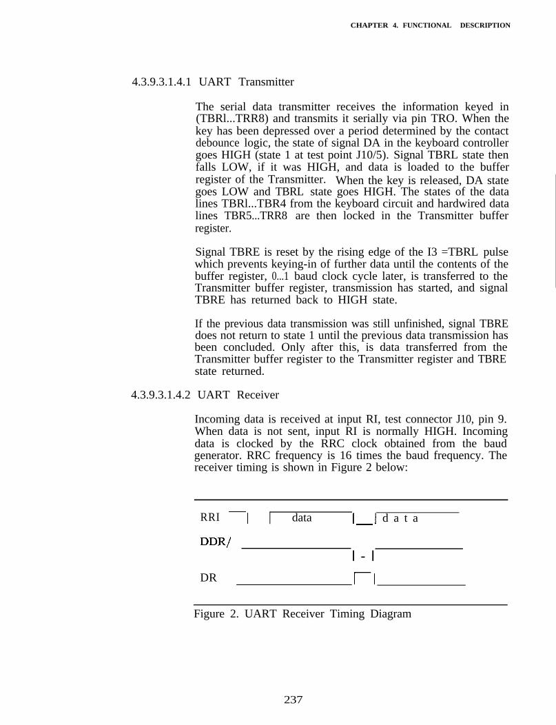
CHAPTER 4. FUNCTIONAL DESCRIPTION
4.3.9.3.1.4.1 UART Transmitter
The serial data transmitter receives the information keyed in(TBRl...TRR8) and transmits it serially via pin TRO. When thekey has been depressed over a period determined by the contactdebounce logic, the state of signal DA in the keyboard controllergoes HIGH (state 1 at test point J10/5). Signal TBRL state thenfalls LOW, if it was HIGH, and data is loaded to the bufferregister of the Transmitter. When the key is released, DA stategoes LOW and TBRL state goes HIGH. The states of the datalines TBRl...TBR4 from the keyboard circuit and hardwired datalines TBR5...TRR8 are then locked in the Transmitter bufferregister.
Signal TBRE is reset by the rising edge of the I3 =TBRL pulsewhich prevents keying-in of further data until the contents of thebuffer register, 0...1 baud clock cycle later, is transferred to theTransmitter buffer register, transmission has started, and signalTBRE has returned back to HIGH state.
If the previous data transmission was still unfinished, signal TBREdoes not return to state 1 until the previous data transmission hasbeen concluded. Only after this, is data transferred from theTransmitter buffer register to the Transmitter register and TBREstate returned.
4.3.9.3.1.4.2 UART Receiver
Incoming data is received at input RI, test connector J10, pin 9.When data is not sent, input RI is normally HIGH. Incomingdata is clocked by the RRC clock obtained from the baudgenerator. RRC frequency is 16 times the baud frequency. Thereceiver timing is shown in Figure 2 below:
RRI --I data I-1 d a t a
DDR/l - l
DR riFigure 2. UART Receiver Timing Diagram
237
CHAPTER 4. FUNCTIONAL DESCRIPTION
During the first stop bit, data is transferred from the Receivingregister into the Receiver’s buffer register, RBR. One clock cyclelater, the data ready signal, DR, goes HIGH. After approximately3µs (created by resistor RA1/3-4, and capacitor C4) the state atpin 3 of circuit U5 goes LOW. This is connected to the UART'sinput DRR which resets the output DR. After another 3µs, thestate at U5, pin 3, and the input signal DRR goes HIGH and thecircuit is ready to receive a new character.
4.3.9.3.1.5 RS-232C Transmitter
The RS-232C Transmitter is comprised of operational amplifierU3 (LM 124). The serial data signal, TRO, coming from theUART Transmitter is brought to the inverting input of the op.amplifier. A ref. voltage of approximately 1.7V is obtained byresistors RA3/1-2 and RA2/9-10. Here, U3 has the function ofan inverting comparator which, at the same time, converts theTTL-level voltage into an RS-232C-compatible voltage. Theoperational amplifier is protected against overvoltages and shortcircuits by diode bridge Dl and resistor R6. Outgoing RS-232Cdata is brought to terminal strip El, pin 3.
4.3.9.3.1.6 RS-232C Receiver
Incoming RS-232C data is brought to terminal strip El, pin 2.R5 and D3 protect the input against overvoltages beyond + 15V.RA3/3-4 provides a load resistance of 10 k ohm for the input andinsures that the unconnected input is kept at state 0. RA3/5-6and C7 form a low-pass filter (time constant: 10 µs) preventingfurther passage of RF interference.
Jumper J5 enables selection of two distinct inputs. When usingthe RS-232C interface, jumper J5 must be in position l-2. Thelevel change from RS-232C (+ 12V) is effected by NAND gate5. Diodes in series at the input of the circuit limit incomingvoltage to between OV and +5V and, at the same time, the circuitinverts the signal so that it can be fed directly into the UARTreceiver. The signal for the UART is taken to test connector J10,pin 9.
238
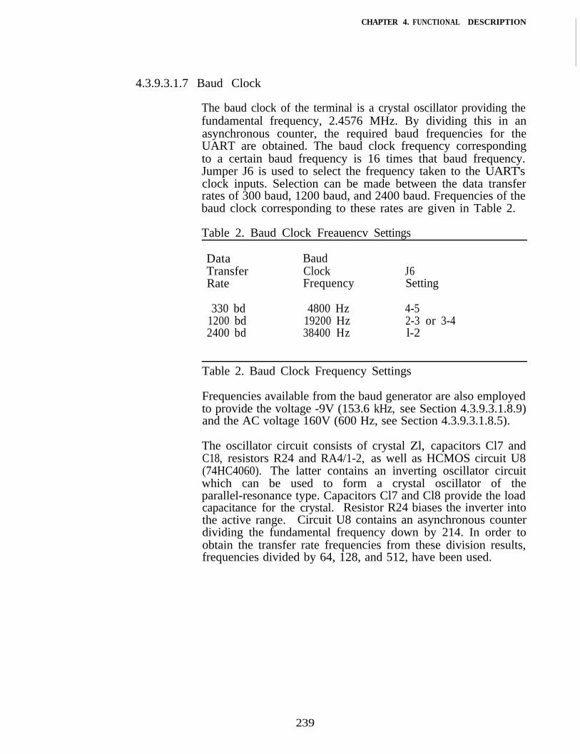
CHAPTER 4. FUNCTIONAL DESCRIPTION
4.3.9.3.1.7 Baud Clock
The baud clock of the terminal is a crystal oscillator providing thefundamental frequency, 2.4576 MHz. By dividing this in anasynchronous counter, the required baud frequencies for theUART are obtained. The baud clock frequency correspondingto a certain baud frequency is 16 times that baud frequency.Jumper J6 is used to select the frequency taken to the UART'sclock inputs. Selection can be made between the data transferrates of 300 baud, 1200 baud, and 2400 baud. Frequencies of thebaud clock corresponding to these rates are given in Table 2.
Table 2. Baud Clock Freauencv Settings
Data BaudTransfer ClockRate Frequency
J6Setting
330 bd 4800 Hz 4-51200 bd 19200 Hz 2-3 or 3-42400 bd 38400 Hz l-2
Table 2. Baud Clock Frequency Settings
Frequencies available from the baud generator are also employedto provide the voltage -9V (153.6 kHz, see Section 4.3.9.3.1.8.9)and the AC voltage 160V (600 Hz, see Section 4.3.9.3.1.8.5).
The oscillator circuit consists of crystal Zl, capacitors Cl7 andC18, resistors R24 and RA4/1-2, as well as HCMOS circuit U8(74HC4060). The latter contains an inverting oscillator circuitwhich can be used to form a crystal oscillator of theparallel-resonance type. Capacitors Cl7 and Cl8 provide the loadcapacitance for the crystal. Resistor R24 biases the inverter intothe active range. Circuit U8 contains an asynchronous counterdividing the fundamental frequency down by 214. In order toobtain the transfer rate frequencies from these division results,frequencies divided by 64, 128, and 512, have been used.
239
CHAPTER 4. FUNCTIONAL DESCRIPTION
4.3.9.3.1.8 Display
4.3.9.3.1.8.1 Operation of the Display Module
The display of the CTH 12 is a 16-character, alphanumeric LCDmodule. The module is comprised of the display control circuits,a processor, and the required storage devices. There are three(3) types of memory:
m 80-Character RAM to Hold Display Data
- 8-Character Characters Memory to retain eight (8) charactersof the User’s Choice
- 192-Character ROM for a permanent retention of thefollowing (See Table 3):
- 96 Alphanumeric Characters
- 64 Katakana Characters
- 32 Symbols
The characters are formed by means of a 5 x 7 dot matrix.Display control is via the eight-bit bus. An electro-luminescentlight behind the display provides lighting as required.
4.3.9.3.1.8.2 Operation of the Display Initialization Circuit
The display module is automatically initialized when power isturned ON. The following commands are carried out duringinitialization:
1. Memories Cleared
2. Operating Mode Set as Follows:
DL = 1: O-bit busN = 0: Single-Line DisplayF = 0: 5 x 7 Display Mode
2 4 0
CHAPTER 4. FUNCTIONAL DESCRIPTION
3. Display ON/OFF:
D = 0: Display OFFC = 0: Cursor Not VisibleB = 0: No Flashing
4. Selecting Input Mode:
I/O = 1: Address IncrementationS = 0: No Transfer
5. DD RAM Addressing Selected
Note: If power for the system is connected incorrectly asfar as the display is concerned, it is possible thatthe display is not initialized.
Repeat the connection if necessary.
241
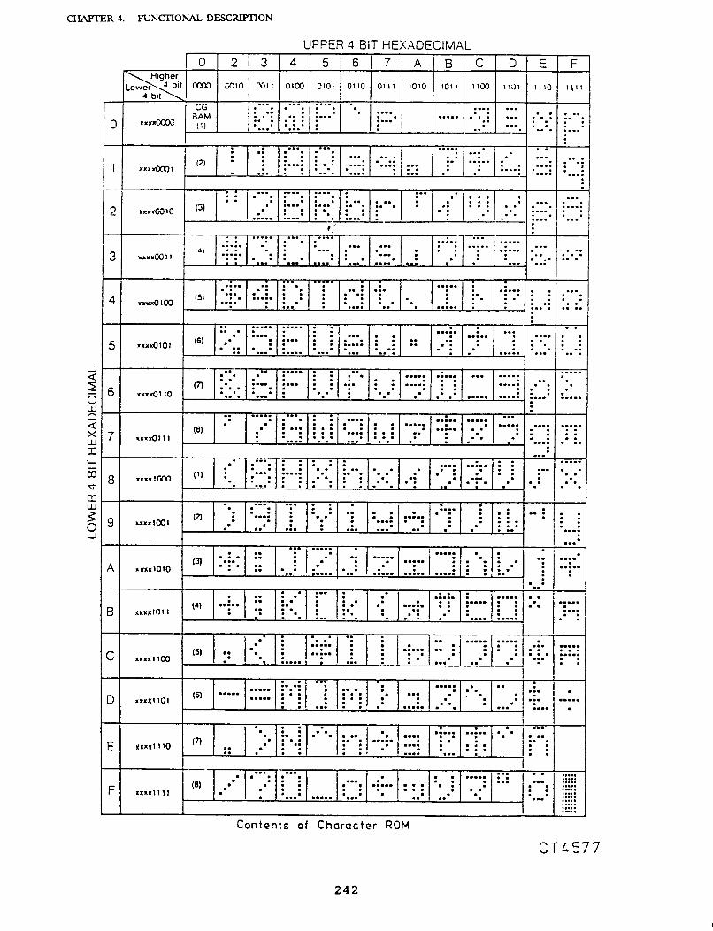
CHAPTER 4. FUNCTIONAL DESCRIPTION
4.3.9.3.1.8.3 Display Control
The 8-bit parallel data received from the UART receiver is takento the display module as follows: The seven (7) lowermost bitsare brough directly to the 8-bit bus of the display; whereas theupper-most data bit RBR8 is used to control the RS input of thedisplay. The RS input signal determines whether the informationreceived from the data bus is interpreted as a control commandor as character data:
RS = 0: Control CommandRS = 1: Character Data
The uppermost data bit DB7 of the display bus is controlled bya separate register, U7, provided with separate set and resetcontrol commands. See Section 4.3.9.3.1.8.4.
The data read timing signal E is derived from signal DR of theUART received via circuit U6/12. The signal is also taken totest connector J10, pin 4. In its normal state, signal E is thesame as signal DRR inverted. In addition to inverting the signalDR, OR gate 6 provides two safeguards: Further passage of anextra DR signal generated during power-up is prevented byholding, by means of signal MR, signal E LOW for the durationof the initial reset function. Also, if a character received fromthe serial data path is faulty and an FE fault is created (i.e., thestop bit is not found at the correct point), this character is notsent to the display because the DR pulse is prevented by signalFE from reaching E.
In principle, it is‘ possible to read the contents of the memoriesof the display module. This feature, however, cannot be used toadvantage in the CTH 12. Also, the R/W control input ispermanently connected to position W so that only data writinginto the display module memories is possible.
4.3.9.3.1.8.4 DB7 Control Logic
The most significant data bit RBR8 of the UART receiver is usedto control the RS input of the display. Separate set and resetcommands are, therefore, needed for controlling the mostsignificant bit, DB7, of the display data bus.
243
CHAPTER 4. FUNCTIONAL DESCRIPTION
DB7 is controlled by the register circuit U7 output. The registercan be set or reset by setting the least significant data bit comingfrom the UART at 1 or 0. The register is clocked by circuits U5and U6 which decode incoming control commands so that U7 willreceive a clock pulse only when a control command of thefollowing format is issued to the display:
D7 6 5 4 3 2 1 0
0 01 (DL)(N) (F) 0 0 = DB7 Reset
0 01 (DL)(N) (F) 0 1 = DB7 Set
4.3.9.3.1.8.5 Display Illumination
To enable display reading in conditions of insufficient lighting, anelectroluminescent light set beneath the display module providesa greenish illumination for the display.
The electroluminscent light requires a high-voltage AC supply.The 600 Hz rectangular wave from the baud generator is used forthis purpose. Because of lifetime limitations, a light-dependentresistor (LDR) is used in the El supply circuit. This turns OFFthe illumination when there is sufficient light for reading.Transistor Q5 forms a level converter, 5V to 12V, and the powerstage consisting of transistors Q3 and Q4 feeds a 12Vpprectangular wave to the transformer via capacitor C8.Transformer Tl raises the voltage to approximately 160Vpp forthe El light.
4.3.9.3.1.8.6 Display Heating
Because the lowest operating temperature of the LCD display is-20°C, a display-heating arrangement is necessary in conditionsof extreme cold.
The heater element is attached to the steel frame of the displayby self-adhesive tape for immediate conduction of heat to theLCD module. The method avoids heating the terminal itself anda sufficient temperature rise (about +40°C) is obtained using apower of approximately 2.5 W. This keeps the display operatingdown to an ambient temperature of about -60°C. On the otherhand, display temperature must not be allowed to rise above+60°C. A temperature sensor (Ul) in the heater control circuithas been provided to measure the temperature inside the case.Ul is a semiconductor sensor giving an output voltageproportional to temperature (10mV/°K).
244
CHAPTER 4. FUNCTIONAL DESCRIPTION
Circuit U3 forms a comparator connecting base current to theDarlington transistor, Ql, when the voltage over the temperaturesensor Ul is less than the voltage produced by the voltage divider,R15 and R16. A hysteresis of approximately 100mV at thecomparator, brought about by resistor R14, corresponds to atemperature of approximately 10°C. The nominal heater switch-onand switch-off temperatures are:
- Switch-on: -12°C (10°F)- Switch-off: - 2°C (28°F)
Ql base current is determined by resistor R10 and thebase-emitter junction of Ql is protected against negative voltagesby diode D2. Heating power is adjusted by resistor R3. Theheater element resistance is 50 ohms. With the R3 value of 8.2ohms, heating current is 205mA and power is 2.5 W.
4.3.9.3.1.8.7 Initial Reset Circuit
The initial reset circuit is comprised of D-register, U7, resistorRAl/l-2, and capacitor C14. When power is turned ON and the5V supply goes up, Cl4 is charged via resistor RAl/l-2. Theclock input of the D-register is connected to ground; likewise,input R. When input S is also zero, the register is set into state1. As voltage at Cl4 goes up, input W/ is turned into state 1,whereupon the register is reset by input R/. The duration of thereset pulse is determined by the RC time constant ofapproximately 50ms.
The reset pulse functions are:
- Reset DB7 Bit- Inhibit Key-In Display- Inhibit DB7 Bit Setting- Reset UART Circuit- Reset Baud Clock Counter
The voltage of the initial reset circuit is also brought to testconnector J10, pin 10.
4.3.9.3.1.8.8 + 5V Supply
The supply voltage of the terminal is + 12V. From this voltage,the logic supply voltage is produced by an adjustable linearregulator (U2). The voltage is determined by resistors R12 andR13 which also perform the function of minimum-load for thecircuit. Capacitors Cl, C2, C3, C12, C13, C15, and C16, are filtercapacitors for the logic circuits. The +5V operating voltage isbrought to test connector J10, pin 3.
245
CHAPTER 4. FUNCTIONAL DESCRIPTION
4.3.9.3.1.8.9 -9V Supply
A negative voltage is generated for display biasing and theRS-232C interface. The -9V supply voltage is produced from the+ 12V DC supply by first creating a 153.6 kHz AC voltage(transistors Q6 and Q7) and rectifying it (diodes D10 and Dll).
The voltage passed on to the display is formed by first limitingthe negative voltage to -5V by means of a zener diode. Thetrirmner, R22, enables adjustment of the display biasing voltagewithin the range -5.lV to +5.lV.
4.3.9.3.2 Connection Signals
Connector El terminals, interface signals, colors, and theMS-connector pins, of the standard interface cable of CTH 12 are:
Table 4. Signals of CTH 12
E lTerminal Signal Color
1 (Not Used) -----
2 Brown
3 RXD Red
4 (Not Used) -----
5 (Not Used) -----
6 FLAG Blue
7 GND Green
8 + 12V White
9 (Not Used) -----
10 (Not Used) -----
MSPin
---
B
C
---
---
G
F
H
- - -
---
Explanation
-------------------
Data In(To Terminal)
Data Out(From Terminal)
-------------------
-------------------
Signalling ofMaintenanceTerminal Presence
Common Ground
Power Supply
-------------------
-------------------
Table 4. Signals of CTH 12
246
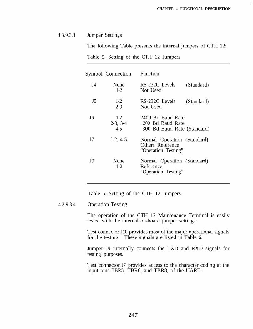
CHAPTER 4. FUNCTIONAL DESCRIPTION
4.3.9.3.3 Jumper Settings
The following Table presents the internal jumpers of CTH 12:
Table 5. Setting of the CTH 12 Jumpers
Symbol Connection Function
J4 None1-2
RS-232C LevelsNot Used
(Standard)
J5 l-22-3
RS-232C LevelsNot Used
(Standard)
J6 1-2 2400 Bd Baud Rate2-3, 3-4 1200 Bd Baud Rate
4-5 300 Bd Baud Rate (Standard)
J7 l-2, 4-5 Normal Operation (Standard)Others Reference“Operation Testing”
J9 None1-2
Normal Operation (Standard)Reference“Operation Testing”
Table 5. Setting of the CTH 12 Jumpers
4.3.9.3.4 Operation Testing
The operation of the CTH 12 Maintenance Terminal is easilytested with the internal on-board jumper settings.
Test connector J10 provides most of the major operational signalsfor the testing. These signals are listed in Table 6.
Jumper J9 internally connects the TXD and RXD signals fortesting purposes.
Test connector J7 provides access to the character coding at theinput pins TBR5, TBR6, and TBR8, of the UART.
247
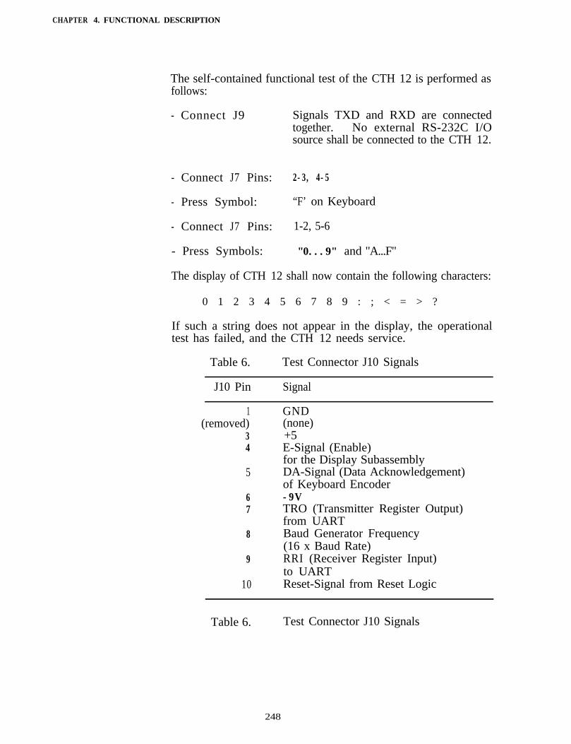
CHAPTER 4. FUNCTIONAL DESCRIPTION
The self-contained functional test of the CTH 12 is performed asfollows:
- Connect J9 Signals TXD and RXD are connectedtogether. No external RS-232C I/Osource shall be connected to the CTH 12.
- Connect J7 Pins: 2-3, 4-5
- Press Symbol: “F’ on Keyboard
- Connect J7 Pins: 1-2, 5-6
- Press Symbols: "0...9" and "A...F"
The display of CTH 12 shall now contain the following characters:
0 1 2 3 4 5 6 7 8 9 : ; < = > ?
If such a string does not appear in the display, the operationaltest has failed, and the CTH 12 needs service.
Table 6. Test Connector J10 Signals
J10 Pin Signal
1 GND(removed) (none)
3 +54 E-Signal (Enable)
for the Display Subassembly5 DA-Signal (Data Acknowledgement)
of Keyboard Encoder6 -9V7 TRO (Transmitter Register Output)
from UART8 Baud Generator Frequency
(16 x Baud Rate)9 RRI (Receiver Register Input)
to UART10 Reset-Signal from Reset Logic
Table 6. Test Connector J10 Signals
248
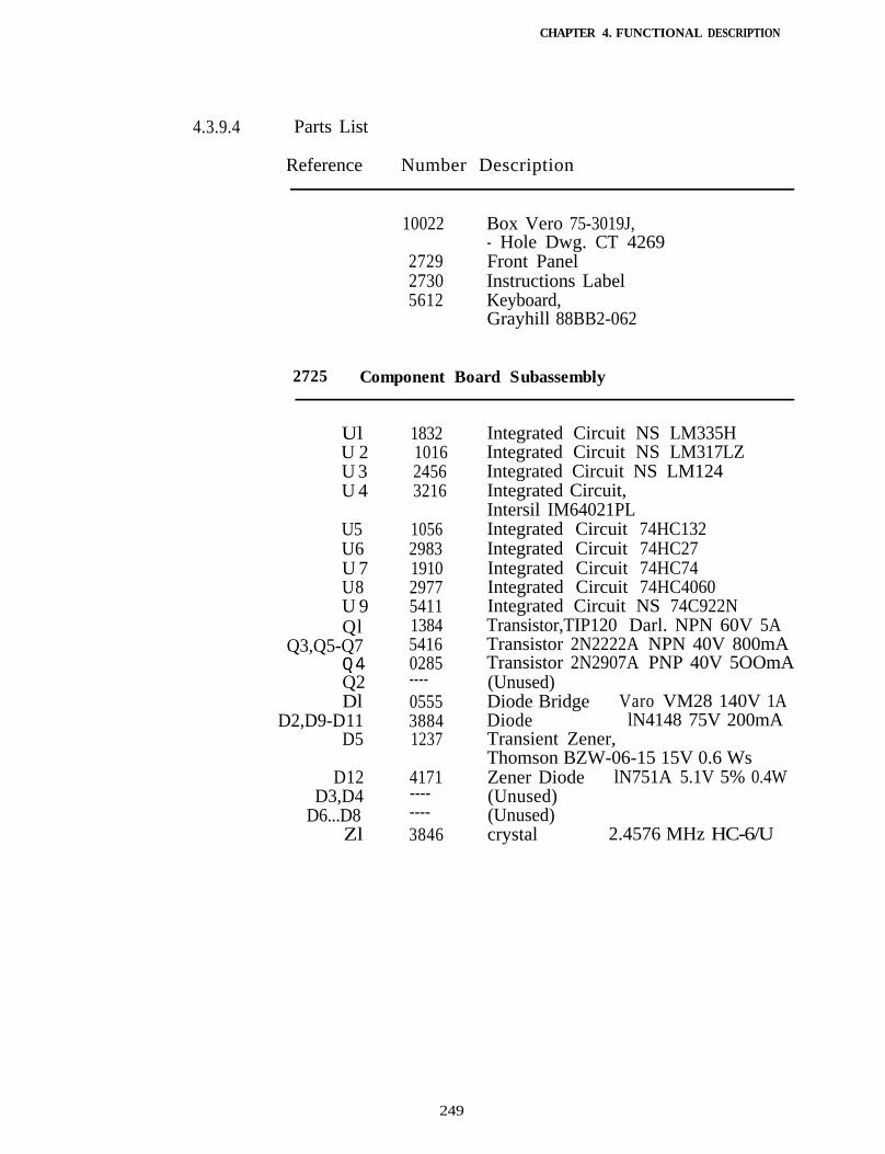
CHAPTER 4. FUNCTIONAL DESCRIPTION
4.3.9.4 Parts List
Reference Number Description
10022
272927305612
Box Vero 75-3019J,- Hole Dwg. CT 4269Front PanelInstructions LabelKeyboard,Grayhill 88BB2-062
2725 Component Board Subassembly
Ul 1832U 2 1016U 3 2456U 4 3216
U5U6U 7U8U 9Ql
Q3,Q5-Q7
Q2Dl
D2,D9-D 11D5
10562983191029775411138454160285----055538841237
D12 4171D3,D4 ----
D6...D8 ----Zl 3846
Integrated Circuit NS LM335HIntegrated Circuit NS LM317LZIntegrated Circuit NS LM124Integrated Circuit,Intersil IM64021PLIntegrated Circuit 74HC132Integrated Circuit 74HC27Integrated Circuit 74HC74Integrated Circuit 74HC4060Integrated Circuit NS 74C922NTransistor,TIP120 Darl. NPN 60V 5ATransistor 2N2222A NPN 40V 800mATransistor 2N2907A PNP 40V 5OOmA(Unused)Diode Bridge Varo VM28 140V 1ADiode lN4148 75V 200mATransient Zener,Thomson BZW-06-15 15V 0.6 WsZener Diode lN751A 5.1V 5% 0.4W(Unused)(Unused)crystal 2.4576 MHz HC-6/U
249
Hugh Black
Q4
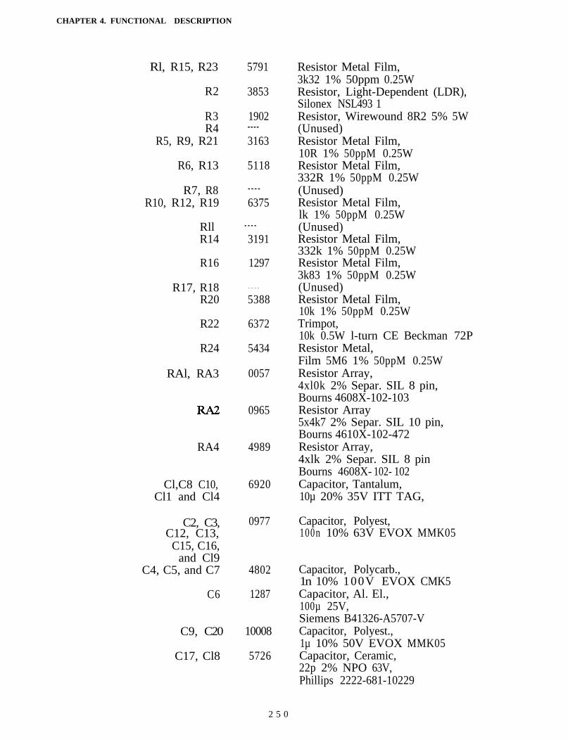
CHAPTER 4. FUNCTIONAL DESCRIPTION
Rl, R15, R23
R2
R3R4
R5, R9, R21
R6, R13
R7, R8 - - - -R10, R12, R19 6375
Rll - - - -R14 3191
R16 1297
R17, R18R20
R22
R24
RAl, RA3
RA4 4989
Cl,C8 C10,Cl1 and Cl4
C2, C3,C12, C13,
C15, C16,and Cl9
C4, C5, and C7
C6
C9, C20
C17, Cl8
5791
3853
1902----3163
5118
- - - -
5388
6372
5434
0057
0965
6920
Resistor Metal Film,3k32 1% 50ppm 0.25WResistor, Light-Dependent (LDR),Silonex NSL493 1Resistor, Wirewound 8R2 5% 5W(Unused)Resistor Metal Film,10R 1% 50ppM 0.25WResistor Metal Film,332R 1% 50ppM 0.25W(Unused)Resistor Metal Film,lk 1% 50ppM 0.25W(Unused)Resistor Metal Film,332k 1% 50ppM 0.25WResistor Metal Film,3k83 1% 50ppM 0.25W(Unused)Resistor Metal Film,10k 1% 50ppM 0.25WTrimpot,10k 0.5W l-turn CE Beckman 72PResistor Metal,Film 5M6 1% 50ppM 0.25WResistor Array,4xl0k 2% Separ. SIL 8 pin,Bourns 4608X-102-103Resistor Array5x4k7 2% Separ. SIL 10 pin,Bourns 4610X-102-472Resistor Array,4xlk 2% Separ. SIL 8 pinBourns 4608X- 102- 102Capacitor, Tantalum,10µ 20% 35V ITT TAG,
0977 Capacitor, Polyest,100n 10% 63V EVOX MMK05
4802
1287
10008
5726
Capacitor, Polycarb.,1n 10% 100V EVOX CMK5Capacitor, Al. El.,100µ 25V,Siemens B41326-A5707-VCapacitor, Polyest.,1µ 10% 50V EVOX MMK05Capacitor, Ceramic,22p 2% NPO 63V,Phillips 2222-681-10229
2 5 0
Tl
E l
Jl, J2,and J5...Jl0
J3
J4P5, P6,
and P7A, P7B
CHAPTER 4. FUNCTIONAL DESCRIPTION
10013
6377
5498
1399
----5143
Transformer,220V/8V 0.2VASpitznagel SPK 2202Terminal Block,3-pole,Lumberg KRE 3Connector Pin Strip,0.1"/0.025" square, Au,Phillips F095 (32-pin stock)Connector 2 pos., AMP 5203152,Foil Receptacle(Unused)Jumper, 2 pos,0.1”/0.025” square, Au,Phillips F088
2726 Cable Subassembly
29242946
100045
4014
Connector MS3 116F12-8PConnector, Cap MIL-C-26482 size 12,
Cable SideCable 8xAWG 18,
Alpha 45068Terminal Bush AWG 18,
Abiko 7575
2727 Display Subassembly
2871
27182964
2965
LCD Display Module,Densitron LM12BlC16CB(H)Heating FoilConnector,1x3 pos. 0.l”, Berg 76308-103Connector,2x7 pos. 0.l”, Berg 76314-107
251
CHAPTER 4. FUNCTIONAL DESCRIPTION
2728 Keyboard Cable Subassembly
Pl, P2 6433 Connector,16 pos., Ribbon Cable Header,Yamaichi FAS-1601-2101-OAF
10044 Polarizing Pin,Yamaichi No. 2/FAS
0571 Ribbon Cable,16xAWG28,Spectrastrip 455-044-16
252
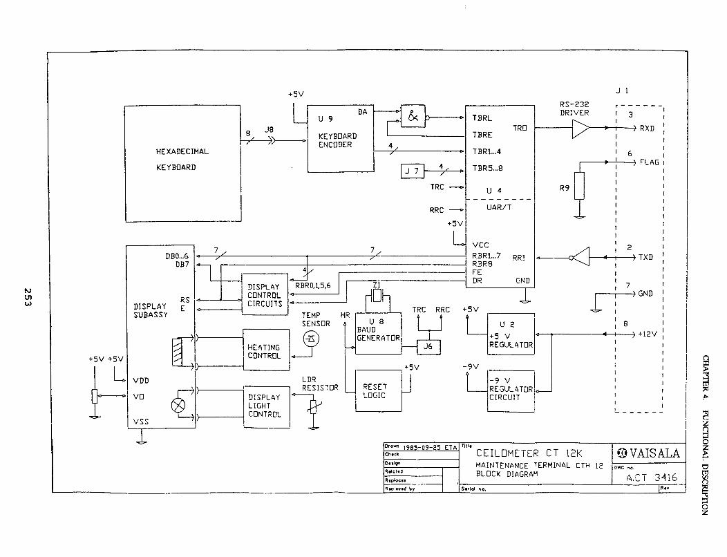
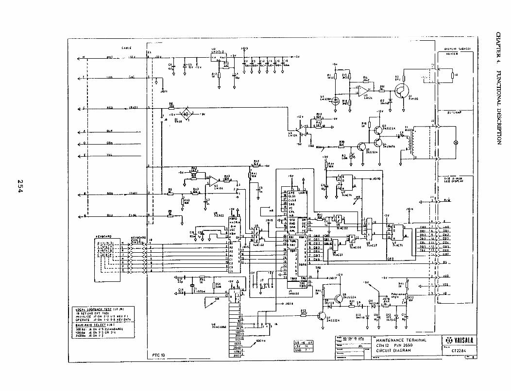
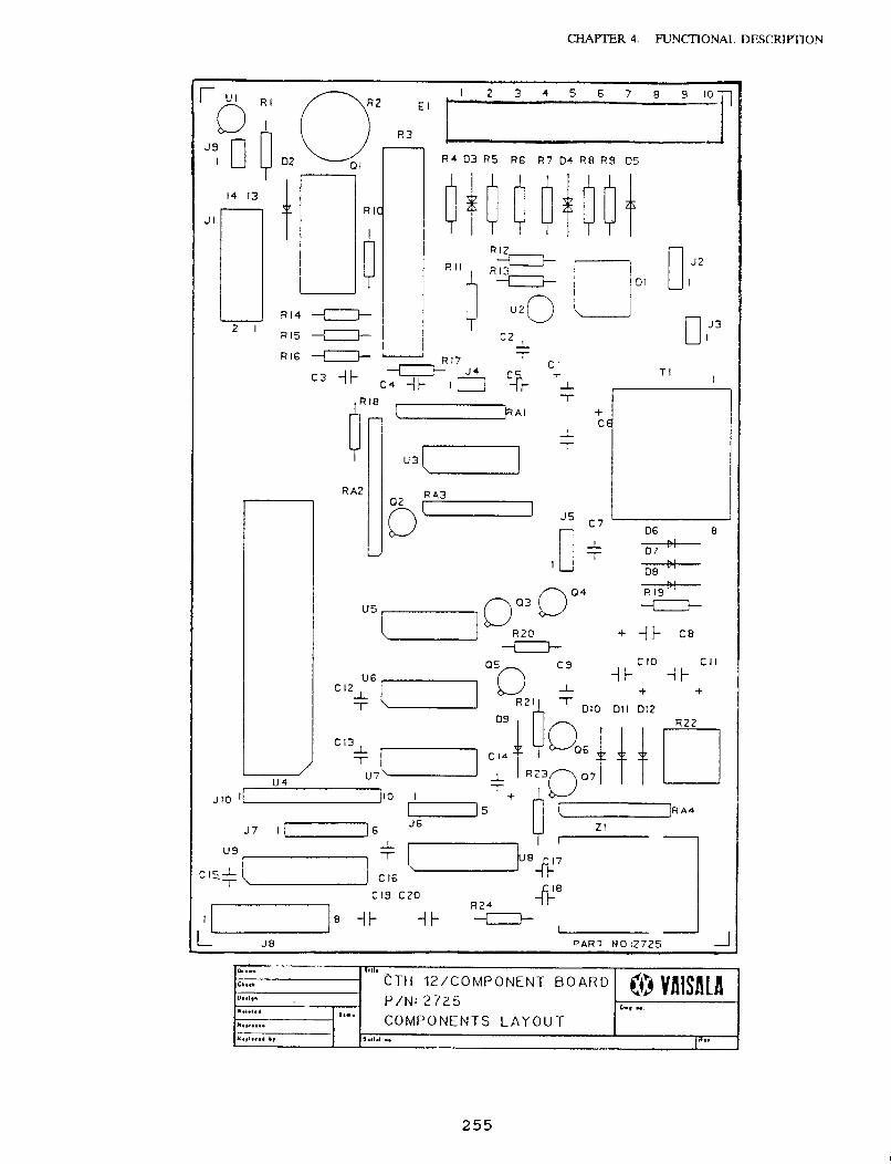

256

257

258

CHAPTER 5. PERIODIC MAINTENANCETABLE OF CONTENTS
SECTION PAGE
5.1 MONTHLY CHECK OF MESSAGE ALARMS 261
5.2 90 DAY CHECK OF WINDOW CLEANLINESSAND CLEANING PROCEDURE 261
5.3 MONTHLY CHECK OF WINDOWCONDITIONER BLOWER 262
259

260

CHAPTER 5. PERIODIC MAINTENANCE
5.1 MONTHLY CHECK OF MESSAGE ALARMS
Check that the data message contains no alarms; see paragraph 6.1.1. If thereare alarms, proceed to troubleshoot following section 6.
5.2 90 DAY CHECK OF WINDOW CLEANLINESS AND CLEANINGPROCEDURE
WARNING! DO NOT LOOK INTO CEILOMETER OPTICS WTHMAGNIFYING GLASS, BINOCULARS OR OTHER MAGNIFYING OPTICSDURING THE COURSE OF PERFORMING THE PROCEDURE BELOW
Inspect the cleanliness of the ceilometer windows. If they are definitelyunclean (e.g. film, streaks, or particles), perform cleaning as detailed below.Otherwise, do not.
A Unplug Window Conditioner connector J2; loosen four (4) knurledscrews holding Window Conditioner to Equipment Cover, andremove Window Conditioner.
B.
C.
D.
E.
F.
Gently dust off all loose particles from the windows with drycleaning cloth of Field Spares Kit, or preferrably with soft brush.
Soak the window surfaces in cleaning alcohol included in the FieldSpares Kit. Let soak for a few minutes.
Gently wipe off liquid with cleaning cloth. Do not rub. Avoidscratching the surface. Turn cloth and gently wipe until dry.
Replace Window Conditioner. Be sure to tighten all four (4)knurled screws well. Reconnect connector to J2.
Wash cleaning cloth,
261
CHAPTER 5. PERIODIC MAINTENANCE
5.3 MONTHLY CHECK OF WINDOW CONDITIONER BLOWER
In connection with Window cleanliness check, observe the performance of theWindow Conditioner Blower by listening to its sound and feeling the air flowto detect signs of wear. If necessary, use the following commands:
AUTO OFFBLOW ON- -AUTO ONCLOS
to control the blower.
If heating is ON, observe that the temperature difference between Blower (TB)and Ambient (TE) is approximately 7°C (=OK). A significantly higherdifference is a sign of reduced blower efficiency.
262

263

264
CHAPTER 6. TROUBLESHOOTING AND REPAIRTABLE OF CONTENTS
SECTION PAGE
6.1 DIAGNOSIS
6.1.1 DATA MESSAGE CONTAINS AN ALARM6.1.2 FSK INTERFACE OPERATION IMPROPER
OR MISSING6.1.3 LOCAL RS-232C INTERFACE OPERATION
IMPROPER OR MISSING6.1.4 CLOUD DETECTION MISSING6.1.5 SUPERFLUOUS DETECTION
6.2 VERIFICATION AND REPLACEMENT
62.16.2.2
6.2.36.2.4
6.2.56.2.66.2.7
6.2.8
6.2.96.2.106.2.116.2.12
PROCESSOR BOARD CTM 12 (REF. Al)UNREGULATED POWER SUPPLYBOARD CTS 12 (REF. A2)OUTPUT INTERFACE BOARD CTI 12 (REF. A3)LIGHT MONITOR BOARD CTL 13 (REF. A5)AND SOLAR SHUTTER CTD 12 (REF. Kl)RECEIVER BOARD CTR 13 (REF. K2)TRANSMITI’ER BOARD CTT 12 (REF. A7)HIGH-VOLTAGE POWER SUPPLYCTP 12 (REF. PSl)TEMPERATURE CONTROL TRANSFORMER(REF. T1)TEMPERATURE CONTROL HEATERS (R1, R2)TEMPERATURE SENSOR (REF. TS1)WINDOW CONDITIONER (115V) (REF. B1)MAINTENANCE TERMINAL CTH 12
6.3 REMOVAL OF CElLOMETER COVERS
6.4 OFFSET CALIBRATION
267
279
280281282
282
287288288
290291
296
297297298298299
299
300
265

266
CHAPTER 6. TROUBLESHOOTING AND REPAIR
THE TROUBLESHOOTING AND REPAIR SHOULD BE DONE AS FOLLOWS:
A. Identify the symptoms of a fault from the alternatives of Chapter 6.1,“Diagnosis,” listed in the manual’s Table of Contents.
B. Go to the Paragraph in question and determine the suspect LRU.
C. Go to the Paragraph in Chapter 6.2, “Verification and Replacement,” whichcovers the suspect LRU. Verify that it is faulty and replace it.
6.1 DIAGNOSIS
6.1.1 DATA MESSAGE CONTAINS AN ALARM
The first line of the Data Message is Status Line 1. The generalformat is as follows:
For full interpretation, turn to Section 3.2. The “S” bits and the“B” indicator are the instrument status indicators of the unit. Theirinterpretation is as follows:
S = 0 No Status Bit Sl...S4 ON for more than 5 minutes
S 1= At least one Status Bit S1...S4 ON for more than5 minutes
B = Space if S = 0
B = “Bel” character if S = 1. Because “bel” is aninvisible character, the alarming line appears onecharacter shorter than normal in a printout.
267
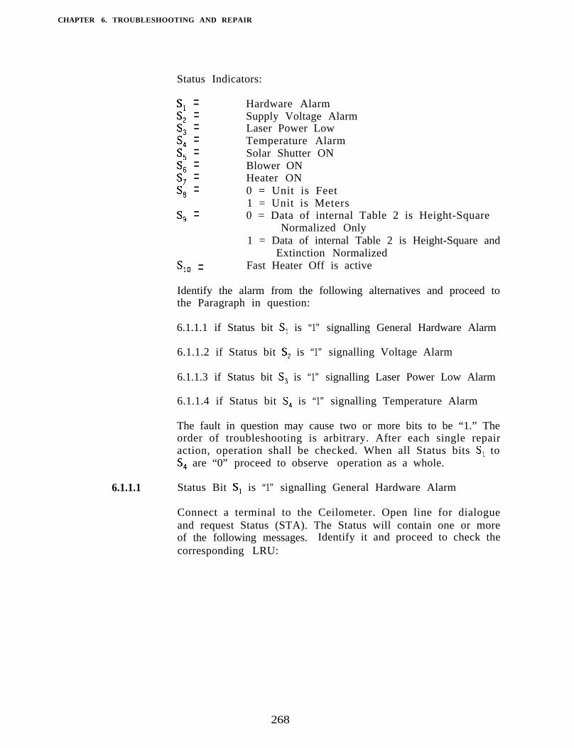
CHAPTER 6. TROUBLESHOOTING AND REPAIR
Status Indicators:
6.1.1.1
s, =s, =s, =s, =s, =s, =s, =s, =
s, =
%I =
Hardware AlarmSupply Voltage AlarmLaser Power LowTemperature AlarmSolar Shutter ONBlower ONHeater ON0 = Unit is Feet1 = Unit is Meters0 = Data of internal Table 2 is Height-Square
Normalized Only1 = Data of internal Table 2 is Height-Square and
Extinction NormalizedFast Heater Off is active
Identify the alarm from the following alternatives and proceed tothe Paragraph in question:
6.1.1.1 if Status bit S, is “1” signalling General Hardware Alarm
6.1.1.2 if Status bit S, is “1” signalling Voltage Alarm
6.1.1.3 if Status bit S, is “1” signalling Laser Power Low Alarm
6.1.1.4 if Status bit S, is “1” signalling Temperature Alarm
The fault in question may cause two or more bits to be “1.” Theorder of troubleshooting is arbitrary. After each single repairaction, operation shall be checked. When all Status bits S, toS, are “0” proceed to observe operation as a whole.
Status Bit S, is “1” signalling General Hardware Alarm
Connect a terminal to the Ceilometer. Open line for dialogueand request Status (STA). The Status will contain one or moreof the following messages. Identify it and proceed to check thecorresponding LRU:
268
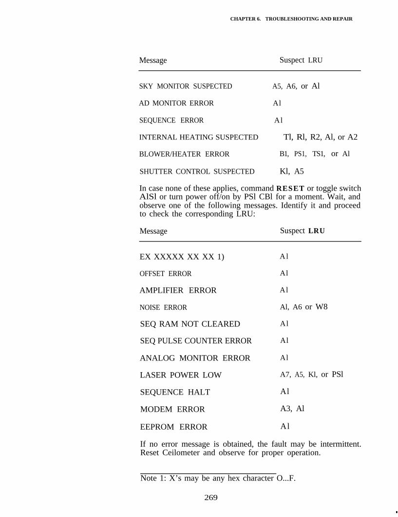
CHAPTER 6. TROUBLESHOOTING AND REPAIR
Message Suspect LRU
SKY MONITOR SUSPECTED A5, A6, or Al
AD MONITOR ERROR Al
SEQUENCE ERROR Al
INTERNAL HEATING SUSPECTED Tl, Rl, R2, Al, or A2
BLOWER/HEATER ERROR B1, PS1, TS1, or Al
SHUTTER CONTROL SUSPECTED Kl, A5
In case none of these applies, command RESET or toggle switchAlSl or turn power off/on by PSl CBl for a moment. Wait, andobserve one of the following messages. Identify it and proceedto check the corresponding LRU:
Message Suspect LRU
EX XXXXX XX XX 1)
OFFSET ERROR
AMPLIFIER ERROR
NOISE ERROR
SEQ RAM NOT CLEARED
SEQ PULSE COUNTER ERROR
ANALOG MONITOR ERROR
LASER POWER LOW
SEQUENCE HALT
MODEM ERROR
EEPROM ERROR
Al
Al
Al
Al, A6 or W8
Al
Al
Al
A7, A5, Kl, or PSl
Al
A3, Al
Al
If no error message is obtained, the fault may be intermittent.Reset Ceilometer and observe for proper operation.
Note 1: X’s may be any hex character O...F.
269
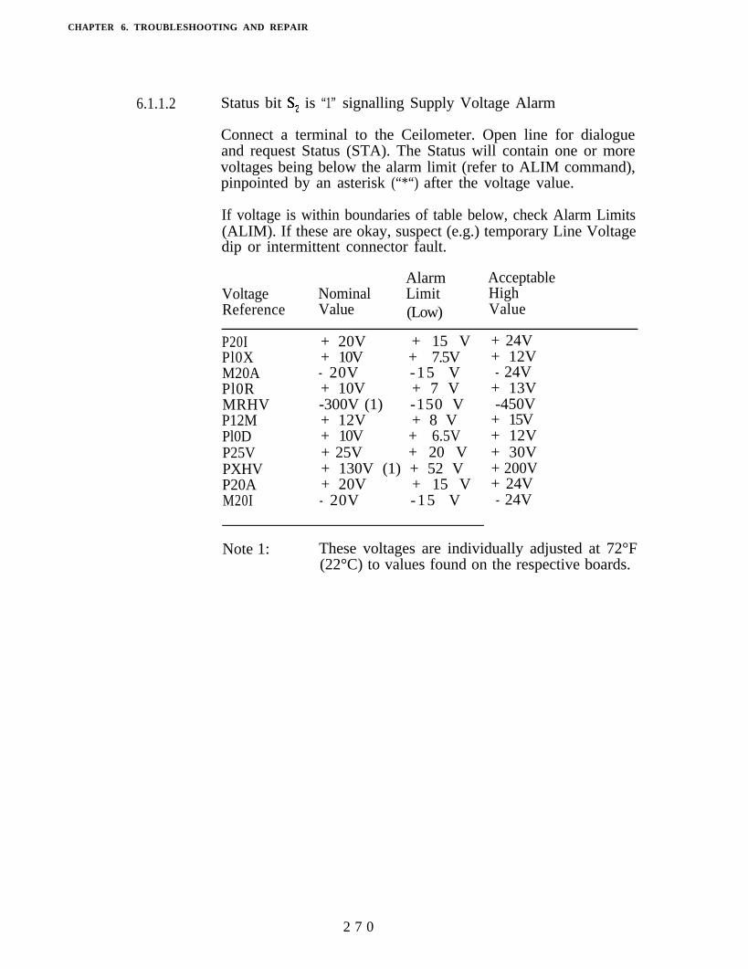
CHAPTER 6. TROUBLESHOOTING AND REPAIR
6.1.1.2 Status bit S, is “1” signalling Supply Voltage Alarm
Connect a terminal to the Ceilometer. Open line for dialogueand request Status (STA). The Status will contain one or morevoltages being below the alarm limit (refer to ALIM command),pinpointed by an asterisk (“*“) after the voltage value.
If voltage is within boundaries of table below, check Alarm Limits(ALIM). If these are okay, suspect (e.g.) temporary Line Voltagedip or intermittent connector fault.
VoltageReference
NominalValue
AlarmLimit(Low)
AcceptableHighValue
P20IPl0XM20APl0RMRHVP12MPl0DP25VPXHVP20AM20I
+ 20V + 15 V+ 10V + 7.5V- 20V -15 V+ 10V + 7 V-300V (1) -150 V+ 12V + 8 V+ 10V + 6.5V+ 25V + 20 V+ 130V (1) + 52 V+ 20V + 15 V- 20V -15 V
+ 24V+ 12V- 24V
+ 13V-450V
+ 15V+ 12V+ 30V+ 200V+ 24V- 24V
Note 1: These voltages are individually adjusted at 72°F(22°C) to values found on the respective boards.
2 7 0
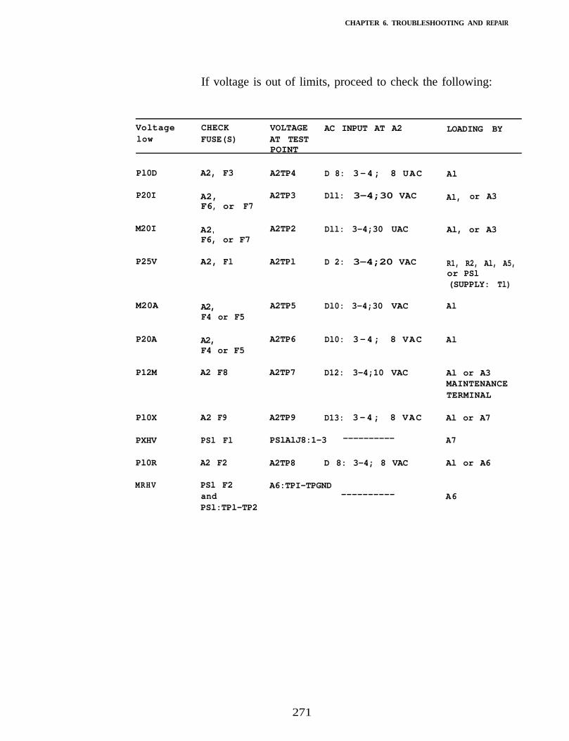
CHAPTER 6. TROUBLESHOOTING AND REPAIR
If voltage is out of limits, proceed to check the following:
Voltage CHECK VOLTAGE AC INPUT AT A2 LOADING BYlow FUSE(S) AT TEST
POINT
Pl0D
P20I
M20I
P25V
M20A
P20A
P12M
Pl0X
PXHV
Pl0R
MRHV
A2, F3
A2,F6, or F7
A2,F6, or F7
A2, Fl
A2,F4 or F5
A2,F4 or F5
A2 F8
A2 F9
PSl Fl
A2 F2
PSl F2andPSl:TPl-TP2
A2TP4 D 8: 3-4; 8 UAC
A2TP3 Dll: 3-4;30 VAC
A2TP2 Dll: 3-4;30 UAC
A2TPl D 2: 3-4;20 VAC
A2TP5 Dl0: 3-4;30 VAC
A2TP6 Dl0: 3-4; 8 VAC
A2TP7 D12: 3-4;10 VAC
A2TP9 D13: 3-4; 8 VAC
PSlAlJ8:1-3 ----------
A2TP8 D 8: 3-4; 8 VAC
A6:TPI-TPGND----------
Al
Al, or A3
Al, or A3
R1, R2, Al, A5,or PSl(SUPPLY: Tl)
Al
Al
Al or A3MAINTENANCETERMINAL
Al or A7
A7
Al or A6
A6
271
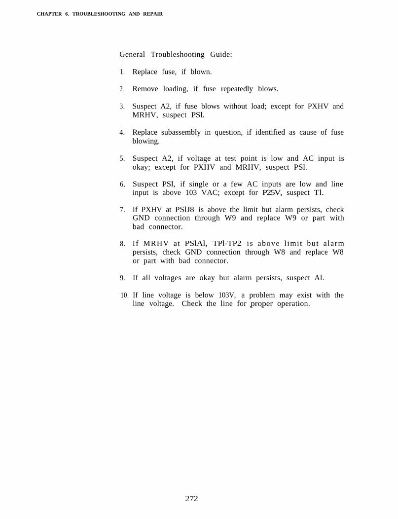
CHAPTER 6. TROUBLESHOOTING AND REPAIR
General Troubleshooting Guide:
1.
2.
3.
4.
5.
6.
7.
8.
9.
10.
Replace fuse, if blown.
Remove loading, if fuse repeatedly blows.
Suspect A2, if fuse blows without load; except for PXHV andMRHV, suspect PSl.
Replace subassembly in question, if identified as cause of fuseblowing.
Suspect A2, if voltage at test point is low and AC input isokay; except for PXHV and MRHV, suspect PSl.
Suspect PSl, if single or a few AC inputs are low and lineinput is above 103 VAC; except for P25V, suspect Tl.
If PXHV at PSlJ8 is above the limit but alarm persists, checkGND connection through W9 and replace W9 or part withbad connector.
If MRHV at PSlAl, TPl-TP2 is above l imi t but a larmpersists, check GND connection through W8 and replace W8or part with bad connector.
If all voltages are okay but alarm persists, suspect Al.
If line voltage is below 103V, a problem may exist with theline voltage. Check the line for proper operation.
272
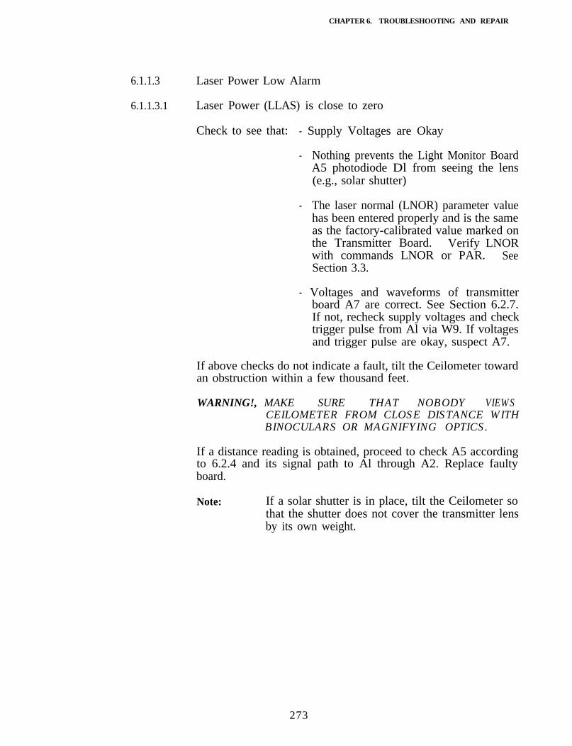
CHAPTER 6. TROUBLESHOOTING AND REPAIR
6.1.1.3 Laser Power Low Alarm
6.1.1.3.1 Laser Power (LLAS) is close to zero
Check to see that: - Supply Voltages are Okay
- Nothing prevents the Light Monitor BoardA5 photodiode Dl from seeing the lens(e.g., solar shutter)
- The laser normal (LNOR) parameter valuehas been entered properly and is the sameas the factory-calibrated value marked onthe Transmitter Board. Verify LNORwith commands LNOR or PAR. SeeSection 3.3.
- Voltages and waveforms of transmitterboard A7 are correct. See Section 6.2.7.If not, recheck supply voltages and checktrigger pulse from Al via W9. If voltagesand trigger pulse are okay, suspect A7.
If above checks do not indicate a fault, tilt the Ceilometer towardan obstruction within a few thousand feet.
WARNING!, MAKE SURE THAT NOBODY VIEWSCEILOMETER FROM CLOSE DISTANCE WITHBINOCULARS OR MAGNIFYING OPTICS.
If a distance reading is obtained, proceed to check A5 accordingto 6.2.4 and its signal path to Al through A2. Replace faultyboard.
Note: If a solar shutter is in place, tilt the Ceilometer sothat the shutter does not cover the transmitter lensby its own weight.
273

CHAPTER 6. TROUBLESHOOTING AND REPAIR
6.1.1.3.2 Laser Power (LLAS) is Below Alarm Limit But Not Close toZero
Note that processor uses maximum pulse frequency (i.e., FREQis 7).
Note the Laser Temperature, TL. It should be below +60°C(+ 140°F). If not, allow the laser to cool by interrupting operationfor a period (AUTO OFF). Check temperature and laser poweragain.
If temperature is well below +60°C (+ 140°F), readjust the LaserSupply voltage according to Paragraph 6.1.1.3.3 If the alarmremains on, replace A7.
6.1.1.3.3 Laser Power Adjustment
Perform this adjustment only at an ambient temperature+ 60°F... + 80°F (15°C...27°C).
Remove equipment covers. Remove transmitter board A7 cover.
WARNING! HIGH VOLTAGE!
Check PAR output message for LNOR value.
Connect voltmeter between TP3 and GND. Increase voltage byadjusting R2 1.
Ceilometer in Maintenance Mode, Frequency 3, Laser on,Sequence on.
Increase voltage towards a maximum of 160V until the LLASvalue in status message equals LNOR-5.
A typical procedure would be as follows:
1) Increase voltage with R21;2) Open line, command AUTO ON, close line;3) Allow time to stabilize;4) Check LLAS = LNOR-55) Repeat, if necessary.
274
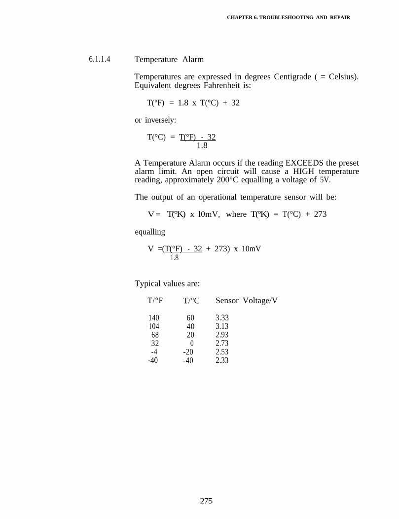
CHAPTER 6. TROUBLESHOOTING AND REPAIR
6.1.1.4 Temperature Alarm
Temperatures are expressed in degrees Centigrade ( = Celsius).Equivalent degrees Fahrenheit is:
T(°F) = 1.8 x T(°C) + 32
or inversely:
T(°C) = T(°F) - 321.8
A Temperature Alarm occurs if the reading EXCEEDS the presetalarm limit. An open circuit will cause a HIGH temperaturereading, approximately 200°C equalling a voltage of 5V.
The output of an operational temperature sensor will be:
V= T(°K) x l0mV, where T(°K) = T(°C) + 273
equalling
V =(T(°F) - 32 + 273) x 10mV1.8
Typical values are:
T/°F T/°C Sensor Voltage/V
140 60 3.33104 40 3.1368 20 2.9332 0 2.73-4 -20 2.53
-40 -40 2.33
275
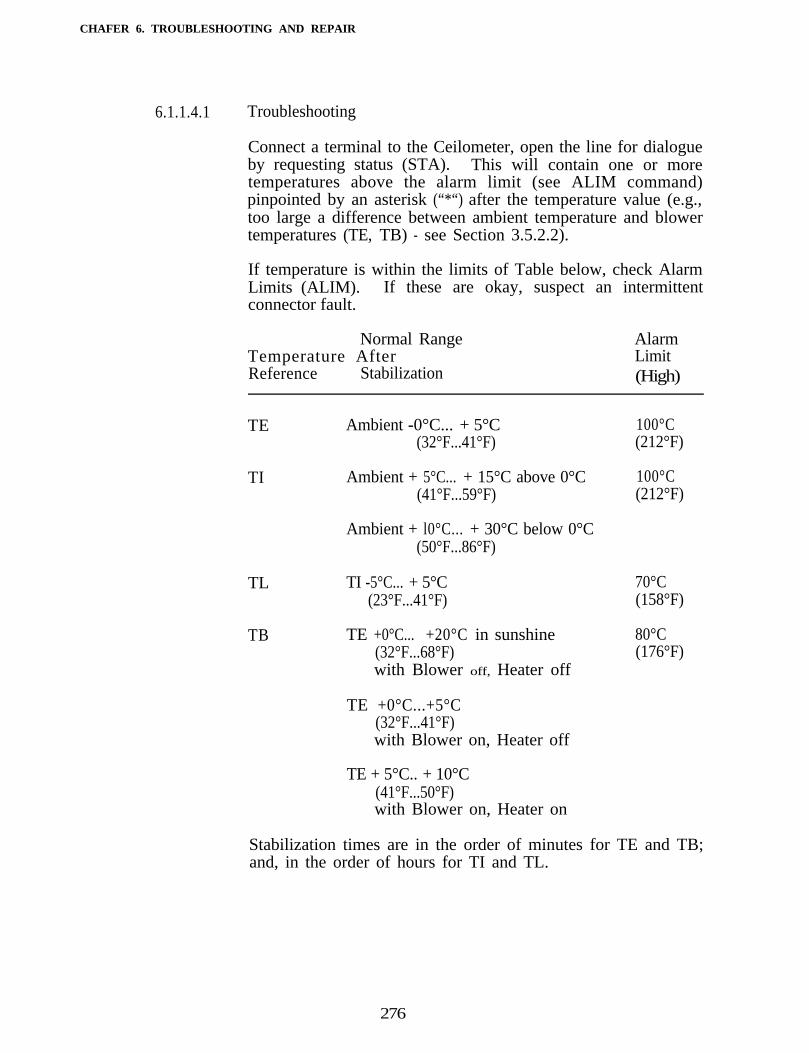
CHAFER 6. TROUBLESHOOTING AND REPAIR
6.1.1.4.1 Troubleshooting
Connect a terminal to the Ceilometer, open the line for dialogueby requesting status (STA). This will contain one or moretemperatures above the alarm limit (see ALIM command)pinpointed by an asterisk (“*“) after the temperature value (e.g.,too large a difference between ambient temperature and blowertemperatures (TE, TB) - see Section 3.5.2.2).
If temperature is within the limits of Table below, check AlarmLimits (ALIM). If these are okay, suspect an intermittentconnector fault.
Normal RangeTemperature AfterReference Stabilization
AlarmLimit(High)
TE Ambient -0°C... + 5°C(32°F...41°F)
TI Ambient + 5°C... + 15°C above 0°C(41°F...59°F)
100°C(212°F)
100°C(212°F)
Ambient + l0°C... + 30°C below 0°C(50°F...86°F)
TL TI -5°C... + 5°C 70°C(23°F...41°F) (158°F)
TB TE +0°C... +20°C in sunshine(32°F...68°F)
80°C(176°F)
with Blower off, Heater off
TE +0°C...+5°C(32°F...41°F)with Blower on, Heater off
TE + 5°C.. + 10°C(41°F...50°F)with Blower on, Heater on
Stabilization times are in the order of minutes for TE and TB;and, in the order of hours for TI and TL.
276
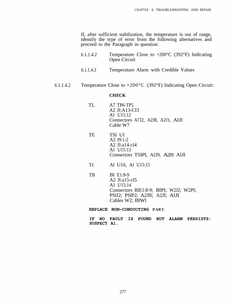
CHAPTER 6. TROUBLESHOOTING AND REPAIR
If, after sufficient stabilization, the temperature is out of range,identify the type of error from the following alternatives andproceed to the Paragraph in question:
6.1.1.4.2 Temperature Close to +200°C (392°F) IndicatingOpen Circuit
6.1.1.4.3 Temperature AIarm with Credible Values
6.1.1.4.2 Temperature Close to +200°C (392°F) Indicating Open Circuit:
CHECK
TL A7 TP6-TP5A2 Jl:A13-Cl3Al U15:12Connectors A7J2, A2J8, A2J1, AlJlCable W7
TE TSl UlA2 J9:1-2A2 Jl:a14-cl4Al U15:13Connectors TSlPl, A2J9, A2J1 AlJl
TI Al U16, Al U15:15
TB Bl E1:8-9A2 Jl:a15-cl5Al U15:14Connectors BlE1:8-9; BlPl; W2J2; W2Pl;PSlJ2; PSlP2; A2Jll; A2Jl; AlJlCables W2; BlWl
REPLACE NON-CONDUCTING PART.
IF NO FAULT IS FOUND BUT ALARM PERSISTS:SUSPECT Al.
277
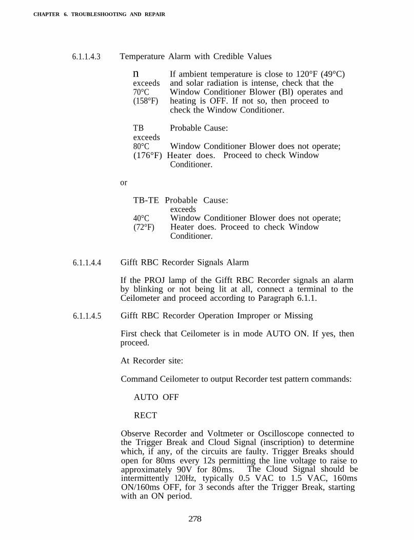
CHAPTER 6. TROUBLESHOOTING AND REPAIR
6.1.1.4.3 Temperature Alarm with Credible Values
n If ambient temperature is close to 120°F (49°C)exceeds and solar radiation is intense, check that the70°C Window Conditioner Blower (Bl) operates and(158°F) heating is OFF. If not so, then proceed to
check the Window Conditioner.
TB Probable Cause:exceeds80°C Window Conditioner Blower does not operate;(176°F) Heater does. Proceed to check Window
Conditioner.
or
TB-TE Probable Cause:exceeds
40°C Window Conditioner Blower does not operate;(72°F) Heater does. Proceed to check Window
Conditioner.
6.1.1.4.4 Gifft RBC Recorder Signals Alarm
If the PROJ lamp of the Gifft RBC Recorder signals an alarmby blinking or not being lit at all, connect a terminal to theCeilometer and proceed according to Paragraph 6.1.1.
6.1.1.4.5 Gifft RBC Recorder Operation Improper or Missing
First check that Ceilometer is in mode AUTO ON. If yes, thenproceed.
At Recorder site:
Command Ceilometer to output Recorder test pattern commands:
AUTO OFF
RECT
Observe Recorder and Voltmeter or Oscilloscope connected tothe Trigger Break and Cloud Signal (inscription) to determinewhich, if any, of the circuits are faulty. Trigger Breaks shouldopen for 80ms every 12s permitting the line voltage to raise toapproximately 90V for 80ms. The Cloud Signal should beintermittently 120Hz, typically 0.5 VAC to 1.5 VAC, 160msON/160ms OFF, for 3 seconds after the Trigger Break, startingwith an ON period.
278
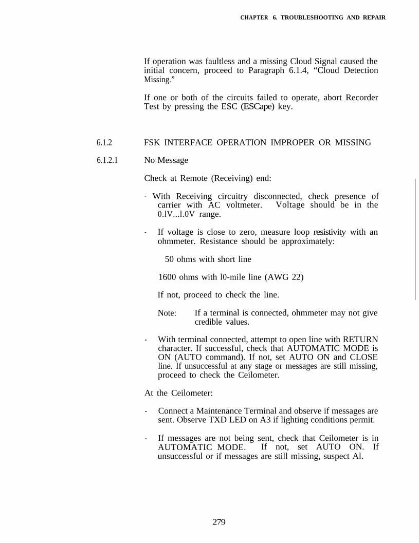
CHAPTER 6. TROUBLESHOOTING AND REPAIR
If operation was faultless and a missing Cloud Signal caused theinitial concern, proceed to Paragraph 6.1.4, “Cloud DetectionMissing.”
If one or both of the circuits failed to operate, abort RecorderTest by pressing the ESC (ESCape) key.
6.1.2 FSK INTERFACE OPERATION IMPROPER OR MISSING
6.1.2.1 No Message
Check at Remote (Receiving) end:
- With Receiving circuitry disconnected, check presence ofcarrier with AC voltmeter. Voltage should be in the0.lV...l.0V range.
- If voltage is close to zero, measure loop resistivity with anohmmeter. Resistance should be approximately:
50 ohms with short line
1600 ohms with l0-mile line (AWG 22)
If not, proceed to check the line.
Note: If a terminal is connected, ohmmeter may not givecredible values.
- With terminal connected, attempt to open line with RETURNcharacter. If successful, check that AUTOMATIC MODE isON (AUTO command). If not, set AUTO ON and CLOSEline. If unsuccessful at any stage or messages are still missing,proceed to check the Ceilometer.
At the Ceilometer:
- Connect a Maintenance Terminal and observe if messages aresent. Observe TXD LED on A3 if lighting conditions permit.
- If messages are not being sent, check that Ceilometer is inAUTOMATIC MODE. If not, set AUTO ON. Ifunsuccessful or if messages are still missing, suspect Al.
279
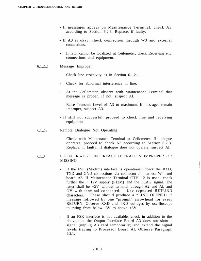
CHAPTER 6. TROUBLESHOOTING AND REPAIR
- If messages appear on Maintenance Terminal, check A3according to Section 6.2.3. Replace, if faulty.
- If A3 is okay, check connection through W3 and externalconnections.
- If fault cannot be localized at Ceilometer, check Receiving endconnections and equipment.
6.1.2.2 Message Improper
- Check line resistivity as in Section 6.1.2.1.
- Check for abnormal interference in line.
- At the Ceilometer, observe with Maintenance Terminal thatmessage is proper. If not, suspect Al.
- Raise Transmit Level of A3 to maximum. If messages remainimproper, suspect A3.
- If still not successful, proceed to check line and receivingequipment.
6.1.2.3 Remote Dialogue Not Operating
- Check with Maintenance Terminal at Ceilometer. If dialogueoperates, proceed to check A3 according to Section 6.2.3.Replace, if faulty. If dialogue does not operate, suspect Al.
6.1.3 LOCAL RS-232C INTERFACE OPERATION IMPROPER ORMISSING
- If the FSK (Modem) interface is operational, check the RXD,TXD and GND connections via connector J4, harness W4, andboard A2. If Maintenance Terminal CTH 12 is used, checkfurther the + 12V supply (P12M) and the FLAG signal. Thelatter shall be +5V without terminal through A2 and Al, andOV with terminal connected. Use repeated RETURNcharacters. These should produce a “LINE OPENED...”message followed by one “prompt” arrowhead for everyRETURN. Observe RXD and TXD voltages by oscilloscopeto swing from below -3V to above +3V.
- If an FSK interface is not available, check in addition to theabove that the Output Interface Board A3 does not short asignal (unplug A3 card temporarily) and extend the signallevels tracing to Processor Board Al. Observe Paragraph6.2.1.
2 8 0
CHAPTER 6. TROUBLESHOOTING AND REPAIR
- Replace board or harness, if found faulty.
- Note that a message being transmitted cannot be interrupted(i.e., dialogue commencement may be delayed for this reason).
6.1.4 CLOUD DETECTION MISSING
If both Gifft RBC Recorder and FSK or RS-232C data messagesare available, check that they agree. If not, proceed to thecorresponding Paragraphs.
If clouds are present and within range without a doubt, checkthat:
- Message contains no alarms. If yes, go to Paragraph 6.1.1.
- Parameter settings are intact. If not, restore them.
- LLAS value is not significantly lower than LNOR value, norsignificantly higher. If so, proceed to check A7, A5, and Al.
- Ceilometer lenses or windows are not obstructed by anything.If so, clear obstructions.
- Noise values and gain selection are credible (i.e., duringbright daytime and clouds present, gain is 0 and noise is 4...10;and, in darkness and twilight with no clouds, gain is 2 andnoise is 1...4. If not, proceed to check A6, and Al.
- Status message after start-up, due to local or remote RESET,contains no alarms. If yes, go to Paragraph 6.1.1.
Above noise numbers are read with command NOIS (see Section3.4) as difference between middle-value and low-value columns.A reliable performance check can be done by tilting theCeilometer on its pedestal toward a nearby horizontal obstruction.
WARNING! MAKE ABSOLUTELY SURE THAT THE LASERBEAM IS NOT VIEWED DIRECTLY WITHBINOCULARS OR ANY OTHER MAGNIFYINGOPTICS!
If the above checks do not reveal cause of malfunction, arrangefor full performance check at authorized Depot or Ceilometermanufacturer.
281
CHAPTER 6. TROUBLESHOOTING AND REPAIR
6.1.5 SUPERFLUOUS DETECTION
If repeated mis-hits are experienced without any apparent cause,check that all parameter values are intact.
Perform offset calibration (see Section 6.4).
If problem persists, return Ceilometer to Depot or Manufacturererfor full performance check.
6.2 VERIFICATION AND REPLACEMENT
6.2.1 PROCESSOR BOARD CTM 12 REFERENCE Al
Verification
In many of the failure cases, the malfunction may be caused bytemporary interference, confusing the Processor software. To clearabnormal conditions, actuate the RESET switch on Al prior toproceeding with verification. RESET is also achieved bytemporarily off/on switching PSlCBl or by RESET command,provided that the device is able to receive commands.
Operating Voltages
Check that the following voltages are inside limits:
J6/8: + 5.0V ±0.25VJ5/ 10: + 12.2V ± 0.8 VJ5/9: -12.2V ±0.8 VJ9/5: + 9.0V ±0.5VJ14/2: + 12.7V ±0.8 VJ19/6: -12.7V ±0.8 VJ19/3: + 6.1V ±0.3 VJ19/4: - 6.1V ±0.3 VJ6/7: + 5.0V ±0.05VJ9/4: + 8.3V ±0.1 VJ9/3: + 1.7V ±0.05VJ9/2: + 0.9V ±0.1 VJ16/10: + 7.1V ±0.3 VJ16/9: + 1.9V ±0.3 VJ19/7: - 4.3V ± 0.3 VJ19/5: + 3.0V ±0.5 V
(+ 5V, Logic Supply)( + 12V, Interface Supply)(-12V, Interface Supply)(+ 9V, Flash ADC Supply)(+ 13V, An. HI Supply)(-13V, An. HI Supply)(+ 6V, An. LO Supply)(- 6V, An. LO Supply)( V5, Mon. ADC Ref.)( RP, Flash ADC HI Ref.)( RC, Flash ADC LO Ref.)( IN, Flash ADC Input)(+ 7.1, Level Shifter Source)(+ 1.9, Level Shifter Return)( AT2, Amp. Test Point 2)( ATl, Amp. Test Point 1)
All the op. voltages are on-board regulated. Their source suppliescan be checked from the STATUS message. Al may also beunplugged to verify the source supplies on A2. +5V and + 12Vare fed via A2 to A3 which may overload them. Unplug A3 todetect this.
282
CHAPTER 6. TROUBLESHOOTING AND REPAIR
CPU Status:
Observe the LED indicators on Al. Green LED should beblinking once a second and Red LED should be dark. If not so,check that +5V and its source supply, + l0VD, are inside limits.If they are, replace Al.
Error Messages Concerning Al Internal Onerations:
Reset the Processor and observe one of the following messages:
AD MONITOR ERRORANALOG MONITOR ERROREX XXXXX XX XX (any hex number 0...F for x)OFFSET ERRORAMPLIFIER ERRORNOISE ERRORSEQUENCE ERRORSEQUENCE RAM NOT CLEAREDSEQUENCE PULSE COUNTER ERRORSEQUENCE HALTEEPROM ERROR
If any one of these appears, check that the jumpers on Al areinstalled according to the Technical Description. If they are, andif the source supply voltages are okay, replace Al.
Supplv Voltage Alarm:
First check other units according to Paragraph 6.1.1.2. If all thevoltages are correct, replace Al. Notice, however, that if cablesW8 and W9 are disconnected or faulty, Pl0X, Pl0R, PXHV, andMRHV, are unmeasureable by Al thus causing an alarm. Evenafter reconnecting W9, the PXHV reading may be invalid forsome time.
Temnerature Alarm:
Check that the negative voltage levels MTE, MTL, MTB, andMTI, correspond to existing temperature (for reference, seeParagraph 6.1.1.4). If they do, but the alarm persists, replace Al.If they don’t, check that sensor source voltage on D2 anode isinside -4.4V to -5.lV. If not, replace Al. Otherwise, suspect thesensor subassemblies and their cables and/or connectors.
283
CHAPTER 6. TROUBLESHOOTING AND REPAIR
Other Alarms:
LASER POWER LOW, with Automatic Mode ON, check theLaser Trigger LTRG (J21/9). This should be high for 60nsapproximately every lms. To measure the pulse, use SQO (J21/3)trigger for oscilloscope. LTRG pulse should appear right afterthe rising edge of SQO. If no pulse seen, unplug W9 from 526.If still not, replace Al; otherwise, suspect W9 or A7. If LTRGis okay, proceed to check LLAS input level. If it is not inconformance with the Laser Power reading, suspect othersubassemblies. Otherwise, replace Al.
SKY MONITOR SUSPECTED; check for LSKY input level, thatit is in conformance with its corresponding Status reading. If not,replace Al. Otherwise, suspect A5 or interconnections.
SHUTTER CONTROL SUSPECTED; check that signal SSON islow. If not, even after Reset, unplug A5, as it may overloadSSON. If still high, replace Al; otherwise, suspect A5 and/or Kl.
BLOWER/HEATER ERROR; enter Maintenance Mode bycommanding AUTO OFF. Set Blower ON and OFF by respectivecommands and check that signal BON is low while ON and opencircuit while OFF. Similar check can be used for Heater controlsignal HON, but it should be noted that Heater shall not beactivated by the Processor if the Blower is OFF. When thesignals are inactive (open-circuit), +25V should be present atcontrol lines, supplied through the relay coils in PSl.
Communication Lines:
Actuate the RESET switch. The Processor should start sendingStatus Data onto serial line. Check that voltage level at TXD(A3/5) swings from below + 1V to above +3V. If no data orincorrect levels, replace Al. If okay, proceed to check TXD(Alc22). The level should swing from below -5V to above +5V.If not, unplug A3 and/or Maintenance Terminal, as they overloadthe line. If correct now, suspect the unplugged LRU. Otherwise,check for shorts on A2 and data cables/connectors. If no shortsfound, replace Al.
284
CHAPTER 6. TROUBLESHOOTING AND REPAIR
For data input, check that IRXD (Alc21) and MRXD (Ala21)swing from below zero to above +5V, when commands aretransmitted to the Ceilometer. IRXD is supplied by A3 andMRXD by Maintenance Terminal (or equivalent). Note that thelines cannot be used simultaneously; one must be low when theother is active. If the levels are not good, suspect A3 orMaintenance Terminal. Otherwise, proceed to check for levelsfrom below + 1V to above +3V at RXD (A3/6). If incorrect,replace Al.
Modem Control:
Check that both ALB and SQT on Al are logic low (< 1.5 Volts),thus enabling the Modem. If not, unplug A3. If still not, replaceAl; otherwise, suspect A3.
Gifft RBC Recorder Control:
Activate Recorder Test according to Paragraph 6.1.7. RBCTshould now be activated (high) for 80 ms every 12 seconds andRBCE alternate for 3 seconds thereafter. Check that levels arefrom below + 1V to above +4V. If not, unplug A3 and repeatthe test. If still not, replace Al; otherwise, suspect A3.
Signal Amnlifier:
With cloud detection missing or repeated mis-hits or high offsetdata base, ‘first check that parameter values are intact andperform Offset Calibration, Section 6.4. If the problem still exists,do the Amplifier test as follows (for reference, see Dwg CT 3536in the Technical Description):
- Unplug W8 at 522.
- Select Single-Pulse/430ns/AMSl by jumper sets J15/J18/J23,respectively.
285
CHAPTER 6. TROUBLESHOOTING AND REPAIR
Simulated Cloud Base should now be detected at ca. 6500 ft.When Double-Pulse is selected by J15, two ranges of signal shouldbe detected: one at 3300 ft; the other at 9700 ft, the latterqualifying as a cloud base. With a terminal connected, open linefor dialogue. Enter Maintenance Mode (AUTO OFF) andcommand the following:
GAIN 0
MEAS (Device is Busy for 1 Second After This)
TAB 0
Now the signal response will be output to the terminal showingbit numbers for each range gate level. Check that the output isapproximately stable 14...17 for the whole range excluding thesimulated base level(s). For reference, see the top figure in CT3536/ TP Response in Sample RAM. If the output numbers arewithin ±20% of those in the figure (AMSl), proceed to checkwith the higher gain; commands:
GAIN 2
MEAS
TAB 0
If the readings are okay also for GAIN 2 (figure below the topone), the Amplifier/Converter and Sequence Control mostprobably are in order, and LRUs other than Al should besuspected.
When returning back to normal operation, set jumpers in J15, J18,and 523, to their original positions, replug W8 to 522, andcommand AUTO ON.
Replacement of Al
Unplug W8 at J22 and W9 at 526. Unplug Al and replace byspare. Replace W8 and W9. Check that jumpers are setaccording to specifications in the Technical Description. SwitchPower ON and check that Green LED starts blinking. Set LNORas described in Paragraph 6.2.6. Perform Offset Calibrationaccording to Section 6.4. Check parameters according to 3.3.
286
CHAPTER 6. TROUBLESHOOTING AND REPAIR
6.2.2 UNREGULATED POWER SUPPLY BOARD CTS 12REFERENCE A2
Verification
Supply Voltages
Check suspect supply voltage AC input from PSl or TSl. Checksuspect voltage (DC) at A2 test points and connectors accordingto 6.1.1.2. Check voltage with and without loading. If loadingcauses significant reduction, check waveform with oscilloscope.If full or half-wave rectified form is observed, replace A2
Signal Connections
Trace signal connections from connector to connector with anohmmeter and/or oscilloscope to determine possible break.
Temperature Control Reiavs
- Check that switch Sl on A2 is in position ON.
- Apply temperature differences between l0°F...80°F (-l0°C...-+30°C) with cold spray and fingers to Processor Board Al,temperature sensor U16. Signals RELl and REL2 swing fromapproximately + 12V to -12V when chilling from 80°F to10°F; first RELl, then REL2.
If relays operate, the sound can be heard.
- Feel the heat at Temperature Control Heaters Rl and R2.The heating can barely be felt at simulated temperaturesbetween 30°F...70°F (0°C...20°C) but can be felt very wellbelow simulated temperature 30°F (0°C).
If relay drive signals are okay and heaters Rl and R2 have thespecified resistivity (see Section 6.2.10), then replace A2.
Replacement
Unplug Al and A3, disconnect all connectors, and unscrew thefour (4) screws holding the board to the board frame. Unplugthe board from the two (2) plastic standoffs, and use pliers topress plastic springs. Replace in reverse order. Check that theswitch positions are: Sl ON, S2 NORMAL.
Perform offset calibration as per Section 6.4.
287
CHAPTER 6. TROUBLESHOOTING AND REPAIR
6.2.3 OUTPUT INTERFACE BOARD CTI 12 REFERENCE A3
Verification
Check supply voltages at test points. Only -5V is on-boardregulated from -20V; others are supplied via A2. A3 may beunplugged to verify the external supply.
Do a processor RESET and observe the results of the modemself-test.
With a remote modem on, check the carrier detect LED, “CD.”This should be ON = LIT.
Check the Gifft RBC Recorder interface with command RECT(in AUTO OFF = MAINTENANCE MODE). The TriggerBreak should be visible at the “RBCT’ LED, and audible as arelay click-click. If this is not the case, check the input at testpoint J6/7; this should be HIGH for 80ms every 12s. If not, thefault is external. During the break, if a recorder is connected,the voltage between tes t poin ts J9-Jl0 shal l r i se to 90V(approximately).
The cloud signal can further be checked by observing LED“RBCE,” test point J5/9 (120Hz intermittent), and test point J5/7(HIGH for active signal). If the latter toggles at about 3Hz, butone or both of the others deviate, then replace A3; otherwise,proceed to check the external circuits. Suspect Al and/or A2.
Replacement
Unplug W3 at J2. Unplug A3 from A2. Replace with spareboard in reverse order. Check that jumper settings are accordingto specifications in Technical Description.
6.2.4 LIGHT MONITOR BOARD CTL 13 REFERENCE A5 ANDSOLAR SHUTTER CTD 12 REFERENCE Kl
Verification
Check that nothing obstructs monitor photodiodes Dl and D3from seeing their respective light sources.
Check supply voltage between TP3 (+ 17V ± 1V) and TP5 (GND)If not in range, check +25V at cathode of D7. If not present,suspect W5, A2, or Tl.
288
CHAPTER 6. TROUBLESHOOTING AND REPAIR
Laser Power Monitor
If an out-of-range Laser Power Monitor signal, LLAS, has beenobserved but positive cloud or hard-target detection has verifiedlaser operation, check linearity with OV equalling LLAS 0, and5V equalling LLAS 255 ( =max). If this is not the case, suspectW5, A2, or Al.
If V(TP1) is less than 1.5V or greater than 4V with laser ON andpositive cloud or hard-target detection, replace A5.
Skv Light Monitor
Check the voltage at TP2 to be close to OV when no strong lightsource is right above Ceilometer and photodiode D3 is pointedupward; and, check with high-intensity focused light brought rightabove D3 that the voltage increases to a value exceeding 2V. Ifthis is not the case, replace A5. If the sun is shining, then asuitably-positioned mirror can be used instead of the lamp.
Solar Shutter Driver
With D3 covered, check that voltage at TP4 is 2V ±0.lV. Adjustat R13 if necessary. Check that driver Q2 is fully conducting (i.e.,solenoid is energized and flap is open). If not, check that forceon signal SSON is LOW. If it is, replace A5; otherwise, suspectAl, A2, or W5. Check that processor control status is SHUTTEROFF.
Place an intense focused light above D3. Observe V(TP2) toexceed 2V. Observe V(TP4) to decrease to approximately 1V.Observe the shutter to turn ON (i.e., de-energize and release theflap to cover the transmitter lens). If not, check Solar ShutterKl, and replace faulty part.
Remove light. Shutter should open.
Command SHUT ON and SHUT OFF in Maintenance Mode(AUTO OFF). Shutter shall follow. If not, check signal SSON.If not HIGH (+4V or more) after SHUT ON command, checkAl, A2, or W5.
Solar Shutter CTD 12 Reference Kl
Solenoid resistivity should be approximately 40 ohms; check.Check mechanical parts. Adjust or replace if necessary.
289
CHAPTER 6. TROUBLESHOOTING AND REPAIR
Replacement of A5
Turn Ceilometer power OFF. Release connectors. Unscrew thetwo (2) screws holding board mounting block to Optics Frame.Replace new board in reverse order. Turn Ceilometer ON.Observe commencement of normal operation.
Replacement of Kl
Follow installation procedure found with the kit. Remove faultyshutter in reverse order.
6.2.5 RECEIVER BOARD CTR 13 REFERENCE A6
WARNING! HIGH VOLTAGE IS ACCESSIBLE WHEN THERECEIVER BOARD COVER IS REMOVED!
- Check Ceilometer Receiver noise behavior according toParagraph 6.1.4.
- Check voltages:
- V(TP3) - GND should be 5V +0.5V, provided V(L1, eitherlead) - GND is 10V +2V; otherwise, replace A6. If V(L1)is out of limits, suspect A2 or A6.
- Voltage at TP2 should be at value found on sticker on theboard at 25°C (77°F) with a temperature dependency of1.3V/°F (2.3V/°C) for other temperatures. If not, suspect PSlor Wl0.
- Check photodiode current by measuring voltage across R4(10k0) at TPl-TP2. When the receiver lens is covered, thisshould be less than 1mV. In bright daylight, with brightc louds above , t h i s may be a s much a s 0.5V b u t n o tsignificantly more. Artificial light may be used as a substitute.
- Check preamplifier Ql and Q2 operation by placing concaveshield above Ceilometer and measuring the resulting pulsewith laser on, either by connecting an oscilloscope directly toA6J3 after unplugging W8 or at the corresponding Al testpoint. Oscilloscope bandwidth shall be 10MHz minimum.Observe positive pulses in the order of l00mV, length 135ns,repetition rate 620Hz... 1100Hz.
If above conditions are not met, replace A6; otherwise, suspectAl or W8.
290
CHAPTER 6. TROUBLESHOOTING AND REPAIR
Replacement
- Disconnect all connectors. Unscrew hex spacer nuts holdingboard to optics assembly. Pull board down to clear longscrews. Place into bag or box immediately to protect mirror-like infrared-interference-filter. ESPECIALLY AVOIDTOUCHING FILTER WITH FINGERS.
- Replace with new Receiver Board. Observe the same filterprotection precautions! Tighten spacer nuts to approximatelysame tightness felt when loosening them.
- Connect cables, turn Ceilometer ON.
- Replace all covers and perform offset calibration as perSection 6.4. Observe performance with real clouds and no fogor precipitation. Check current signal sum by TOTALcommand. Check several, and note average.
- If cloud detection reliability appears significantly reduced andthe CURRENT SIGNAL SUM obtained is out of range 20...40(See Section 3.3, ‘Total”) in specified conditions, then returnCeilometer to Depot or Manufacturer for thoroughperformance check.
6.2.6 TRANSMITTER BOARD CTT 12 REFERENCE A7
Verification
The absence of laser power can be verified by cloud hits missing,monitored laser ‘power (reference LLAS) being very low--whichshould give a “Laser Power Low” alarm, status bit S, = l--and byusing an external infrared detecting device.
WARNING! DO NOTATTEMPT TO LOOK AT TRANSMITTEROPTICS WITH MAGNIFYING GLASSES,BINOCULARS, ETC.
WARNING! HIGH VOLTAGES ARE ACCESSIBLE WHENTHE TRANSMITTER BOARD IS REMOVED!
291
CHAPTER 6. TROUBLESHOOTING AND REPAIR
Measure the DC voltages:
- TP4-GND + 10V ± 1.5V (Low Voltage Supply)
- TP7-GND + 260V ± 40V (High Voltage Supply)
- TP3-GNDDC-voltage marked on sticker on board, measuredwith laser off (Maintenance Mode) and correctingfor ambient temperature deviation from 70°Ftemperature coefficient approximately lV/°F(1.8V/°C).
- TP6-GND +2.94VDC at 70°F; temperature coefficient5.5mV/°F (l0mV/°C) (laser temperature sensor)
Command AUTO ON and observe the following waveforms withoscilloscope. Note that these are typical forms measured with60MHz or faster Oscilloscope. Lower bandwidth will round offsteep changes (Dwg No. CT 4535).
- If the Trigger pulse input at TP1 is missing or severelydeformed, suspect Al or W9.
- If the input voltage at TP7 is too low, suspect PSl or W7.
- If the temperature sensor voltage TP6-TP5 is too low, suspectAl, A2, or W7.
- If the low voltage supply at TP4 is too low, suspect A2 or W7.
- If voltage at TP7 is okay but TP3 is close to zero, turnCeilometer power OFF, then ON, and check again. Ifoperation is restored, observe it for a period; if the situationis repeated, replace A7.
- In all other cases, and in cases mentioned above, in which acheck of the suspect part has yielded no fault, replace A7.
292
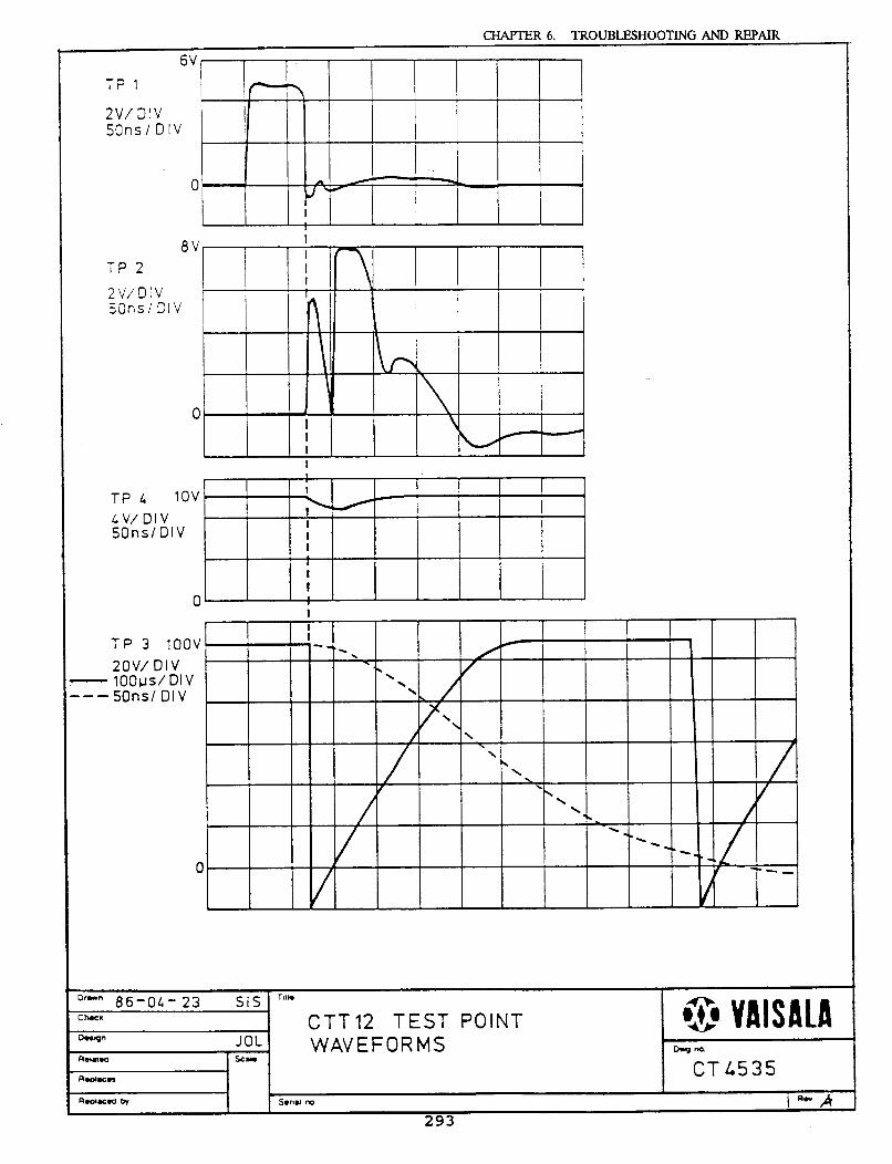
CHAPTER 6. TROUBLESHOOTING AND REPAIR
Replacement
CAUTION: Never look direct& into laser beam coming fromtransmitter optics when laser is enabled (Red LEDon Light Monitor Board is lit when laser is enabled).
Remove all connectors. Unscrew the three (3) spacer nutsholding board to optics assembly. Pull board down clear of longscrews. Insert new board. Tighten spacer nuts to approximatelysame tightness as with the removed board. Plug connectors.
Place diffuser over transmitter lens such that the three notchesin the diffuser ring are lined up with the three pairs of supportscrews located on the lens plate. (Diffuser ring must rest flat onlens plate).
Turn power to the ceilometer on using switch on front panel ofpower supply. Now allow unit to “warm up” for at least l/2 hourwith the external covers replaced on unit.
Connect maintenance terminal to base of unit at connector J4.
Using maintenance terminal command the following:
AUTO OFF (Maintenance Mode)FREQ 3SEQ ONLASE ONAN LLAS
Watch the values now displayed on the maintenance terminal.If the average of these values is not equal to the value listed onthe diffuser then terminate the output and do the following:
If Average is less than the diffuser value (after ±3 tolerance) thencommand:
FREQ 4SEQ ONLASE ONAN LLAS
If Average is more than the diffuser value (after ± 3 tolerance)then command:
FREQ 2SEQ ONLASE ONAN LLAS
294
CHAPTER 6. TROUBLESHOOTING AND REPAIR
Again monitor the values displayed. Repeat the previous step asmany times as it takes (incrementing or decrementing “FREQ” by1 each time) until the average “LLAS” value is equal to thediffuser value (±3). Do not terminate the output when thisaverage value is achieved.
Remove external covers from the unit.
Remove diffuser from lens plate being careful not to scratch lensor hit the light monitor board.
Notice the “LLAS” values now being displayed on the maintenanceterminal. Visually estimate the average of these values and thenterminate the output.
Add 5 to this average, which will be the value for LNOR.
Using the maintenance terminal, command the following(Example):
LNOR 150
NOTE: The actual ‘LNOR” value inputted will be thatcalculated in the previous step.
Command: LNOR: The response seen on the maintenanceterminal should be:
LNOR XXX
(where XXX signifies the value inputted in the previous step).If this is not the case, repeat the previous step and check to makesure the information is transferred correctly.
Command: AUTO ON
Disconnect maintenance terminal from unit.
Replace transmitter optics assembly cover and unit cover. Returnused transmitter board to depot for repair.
295
CHAPTER 6. TROUBLESHOOTING AND REPAIR
Perform offset calibration according to Section 6.4. Set unit intoAutomatic Mode:
AUTO ON
CLOS
Observe operation with real clouds. Observe value of CURRENTSIGNAL SUM with command TOTAL. If cloud detection showsclear signs of uncertainty and value of above SUM is out of range20...40 (See Section 3.3, “Total”) in specified conditions, returnunit to Depot or Manufacturer for thorough performance check.
6.2.7 HIGH-VOLTAGE POWER SUPPLY CTP 12REFERENCE PSl
WARNING! HIGH VOLTAGES!
Verification
Check that the line input voltage is within specified limits.Indicator lamp DSl should be lit regardless of circuit breakersCBl or CB2 positions.
With CBl or CB2 ON, check that all output voltages are presentand within specifications. Check Window Conditioner ControlsBlower ON (Line voltage PSlJ2:l signal LB) and Heater ON(PSlJ2:2 signal LH) with commands:
AUTO OFFBLOW ONHEAT ON
If not okay, check PSl relays Kl and K2, drives BON and HON(active Low), and supply +25V at A2Jll. Suspect Al or A2 ifnot okay; otherwise, replace PSl.
Replacement
Unplug all connectors of PSl. Unscrew four (4) screws at frontand two (2) at rear using the Allen (hex) key found in the FieldSpares Kit. Slide entire power supply out from the front.Replace in reverse order.If the Ceilometer is equipped with receiver CTR 13, R13 has tobe adjusted to it’s maximum (fully clockwise). If the old receiverCTR 12 is being used, adjust Receiver High-Voltage at TPl-TP2with R13 to initial value found on sticker on Receiver Board A6and Quality Assurance documents. Observe temperatureco-efficient 0.83V/°F (1.4V/°C) at temperatures outside 60°F...80°Frange (15°C...27°C). Perform offset calibration as per Section 6.4.
296
CHAPTER 6. TROUBLESHOOTING AND REPAIR
6.2.8 T E M P E R A T U R E C O N T R O L T R A N S F O R M E RREFERENCE Tl
WARNING! HIGH VOLTAGES!
Verification
Check output voltage of transformer, 20VAC ±3V, found on A2(e.g., at diode bridge D2, pins 3-4). Cool down U16 of Al withcold spray to obtain maximum loading. Check voltage with Tldisconnected from A2(J3).
Check line supply voltage outputs at PSlJ3.
Replace faulty part.
Renlacement
- Disconnect connectors f rom A2J3;PSlJ3. Open up cableclamp holding secondary wires to top of Optics Frame.Remove Receiver Cover. Cut bundle ties holding primarywires to Optics Frame lower part.
- Lift plastic feed-through bushing guiding secondary wiresthrough Optics Frame top. Remove wires through slot.Unscrew two (2) screws holding Tl to Optics Frame top.Remove, Tl. Replace in reverse order. Replace cut bundleties with new ones.
6.2.9 TEMPERATURE CONTROL HEATERSREFERENCES Rl AND R2
Verification
Disconnect from A2 connector J2 or J4, respectively, and measureresistance to be 10 ohms ±5%. Replace if not within limits;otherwise, suspect A2, Al or Tl.
Renlacement
- Disconnect from A2. Pull out feed-through bushing from holein Optics Frame wall. Unscrew two (2) screws holding resistorto wall.
- Transfer as much as possible of heat-conducting siliconcompound from replaced resistor to new resistor. Assemblein reverse order.
297
CHAPTER 6. TROUBLESHOOTING AND REPAIR
6.2.10 TEMPERATURE SENSOR REFERENCE TSl
Verification
Check circuit voltage at A2 to be approximately 2.94V at 70°F(21°C), temperature coefficient 5.5mV/°F (l0mV/°C). If not,disconnect TSl at A2J9 and measure an open circuit voltage ofapproximately 5V at A2J9, pins 1 and 2 . Short it and measurea current of approximately 2mA. If the latter measurements arenot okay, suspect Al or A2. Otherwise, replace TSl.
Replacement
- Disconnect from A2J9. Cut bundle ties. Remove air filterfrom vent. Lift TSl from vent. Replace in reverse order.Replace cut bundle ties with new ones.
6.2.11 WINDOW CONDITIONER (1l5V) REFERENCE Bl
WARNING! HIGH VOLTAGES!
Verification
Using maintenance commands, check temperature sensor TB togive credible values. Command BLOW ON, HEAT ON (inMaintenance Mode, AUTO OFF), and observe TB to riseapproximately 12°F (7°C) above ambient (TE) in a few minutes.If temperature rises considerably more, suspect blower operation;if not at all, suspect heater operation.
- Disconnect the Window Conditioner at J2 and measureresistivities:
- Blower circuit, approximately 60 ohms;
- Heater Circuit, 22 ohms.
If these are okay, suspect PSl, Al, or A2; otherwise, replace Bl.
- If the temperature TB is not correct, check the supply circuitas with TSl (Section 6.2.11) and replace Bl if this is correct.Otherwise, suspect PSl, Al or A2.
Replacement
- Disconnect at J2, Loosen four (4) knurled screws holdingWindow Conditioner to Equipment Cover. Lift off. Removecable from guiding clamp at inside. Unscrew four (4) screwsholding Heater-Blower to the housing. Pull downHeater-Blower. Replace in reverse order.
298
CHAPTER 6. TROUBLESHOOTING AND REPAIR
6.2.12 MAINTENANCE TERMINAL CTH 12
A self-test can be performed on the Maintenance Terminal toverify operation. See Section 4.3.9.3.4.
6.3 REMOVAL OF CEILOMETER COVERS
WARNING! WHENEVER WORKING CLOSE TO A CEILOMETER, DO NOTUNDER ANY CIRCUMSTANCES LOOK INTO IT’S OPTICSWITH MAGNIFYING GLASSES, BINOCULARS OR OTHERMAGNIFYING OPTICS, NOR ALLOW ANYBODY ELSE TO DOSO. IT MAY BE HARMFUL TO THE EYES.
1. Disconnect Window Conditioner Connector J2.
2. Loosen four (4) Window Conditioner knurled screws on widesides of Ceilometer.
3. Raise Window Conditioner and place on ground.
4. Open latches of Equipment Cover at lower edge of wide sidesof Ceilometer.
5. Carefully raise the Equipment Cover over the equipment andplace on ground.
IN ALL MAINTENANCE OPERATIONS, PREVENT DUST,PRECIPITATION, ETC. , FROM COLLECTING ON THELENSES! Use temporary covers, if necessary. Especially avoidtouching the lenses with bare hands. Clean lenses, if necessary, withalcohol and a clean, lint-free cloth according to Paragraph 5.2.Cover the Ceilometer by following steps l-5 in a reverse order. Besure to remove temporary lens covers, and to leave circuit breakersCBI and CB2 ON.
299
CHAPTER 6. TROUBLESHOOTING AND REPAIR
6.4 OFFSET CALIBRATION
The instrument offset has been factory-calibrated and in normal conditions noneed for field recalibration exists.
If, however, a part is replaced that has an influence on internal noise behavior,a recalibration shall be performed after restoration of operation. Partsinfluencing noise behavior are:
Al Processor BoardA2 Unregulated Power Supply BoardA6 Receiver BoardA7 Transmitter BoardPS 1 High-Voltage Power SupplyW6 Receiver Low-Voltage CableW7 Transmitter Low-Voltage CableW8 Receiver Signal CableW9 Transmitter Control Cable
If, for some reason, noise hits are more frequent in some ranges than inothers--excluding the self-evident higher probability for high-range noise hitsthan for low-range ones due to lower signal-to-noise ratio--a recalibration isto be performed.
Procedure for Offset Calibration
A. Check that noise conditions are such that difference between two smallestnumbers (average and minimum) seen with command NOIS are 8 orhigher with GAIN 2 and 2 or higher with GAIN 0. Use artificial lightpointed into Receiver, if necessary.
B. With equipment in normal operating configuration (i.e., equipment coverand window conditioner ON), cover the transmitter side aperture of theWindow Conditioner with dark, non-reflecting cloth. If done indoors, usea desk lamp positioned over the receiver as the constant light source.If done outdoors, make sure that ambient light conditions are stable. Forexample wait for a long break in the clouds if there is a broken cloudcover.
C. Perform command sequence:
AUTO OFF (Output: MAINTENANCE MODE)GAIN 0LASE ONSEQ ONCAL 240
300

CHAPTER 6. TROUBLESHOOTING AND REPAIR
D. After 4 minutes, the unit has recorded its offset signature and respondswith:
OFFSET TO EEPROM
and starts listing the offset values obtained. This can be interrupted byhitting the ESC key.
E. Restore normal operation by commanding:
AUTO ONCLOS
and removing the transmitter aperture cover.
F. Observe that performance is okay.
301

302

303

304


