OPA857 Ultralow-Noise, Wideband, Selectable … · IN OUTN OUT R F2 R F1 25 W 25 W CTRL +V S GND...
35
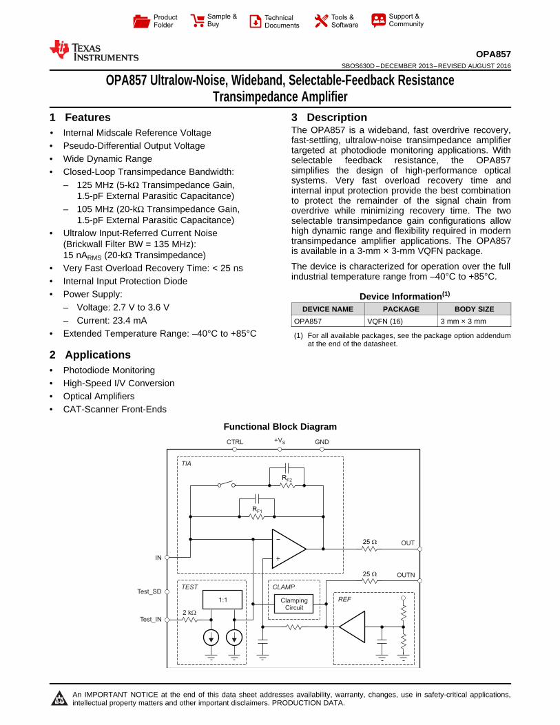
IN OUTN OUT R F2 R F1 25 W 25 W +V S GND CTRL Test_SD Test_IN 1:1 2 kW TIA TEST REF Clamping Circuit CLAMP Product Folder Sample & Buy Technical Documents Tools & Software Support & Community An IMPORTANT NOTICE at the end of this data sheet addresses availability, warranty, changes, use in safety-critical applications, intellectual property matters and other important disclaimers. PRODUCTION DATA. OPA857 SBOS630D – DECEMBER 2013 – REVISED AUGUST 2016 OPA857 Ultralow-Noise, Wideband, Selectable-Feedback Resistance Transimpedance Amplifier 1 1 Features 1• Internal Midscale Reference Voltage • Pseudo-Differential Output Voltage • Wide Dynamic Range • Closed-Loop Transimpedance Bandwidth: – 125 MHz (5-kΩ Transimpedance Gain, 1.5-pF External Parasitic Capacitance) – 105 MHz (20-kΩ Transimpedance Gain, 1.5-pF External Parasitic Capacitance) • Ultralow Input-Referred Current Noise (Brickwall Filter BW = 135 MHz): 15 nA RMS (20-kΩ Transimpedance) • Very Fast Overload Recovery Time: < 25 ns • Internal Input Protection Diode • Power Supply: – Voltage: 2.7 V to 3.6 V – Current: 23.4 mA • Extended Temperature Range: –40°C to +85°C 2 Applications • Photodiode Monitoring • High-Speed I/V Conversion • Optical Amplifiers • CAT-Scanner Front-Ends 3 Description The OPA857 is a wideband, fast overdrive recovery, fast-settling, ultralow-noise transimpedance amplifier targeted at photodiode monitoring applications. With selectable feedback resistance, the OPA857 simplifies the design of high-performance optical systems. Very fast overload recovery time and internal input protection provide the best combination to protect the remainder of the signal chain from overdrive while minimizing recovery time. The two selectable transimpedance gain configurations allow high dynamic range and flexibility required in modern transimpedance amplifier applications. The OPA857 is available in a 3-mm × 3-mm VQFN package. The device is characterized for operation over the full industrial temperature range from –40°C to +85°C. Device Information (1) DEVICE NAME PACKAGE BODY SIZE OPA857 VQFN (16) 3 mm × 3 mm (1) For all available packages, see the package option addendum at the end of the datasheet. Functional Block Diagram
Transcript of OPA857 Ultralow-Noise, Wideband, Selectable … · IN OUTN OUT R F2 R F1 25 W 25 W CTRL +V S GND...
IN
OUTN
OUT
RF2
RF1
25 W
25 W
+VS GNDCTRL
Test_SD
Test_IN
1:1
2 kW
TIA
TEST
REFClampingCircuit
CLAMP
Product
Folder
Sample &Buy
Technical
Documents
Tools &
Software
Support &Community
An IMPORTANT NOTICE at the end of this data sheet addresses availability, warranty, changes, use in safety-critical applications,intellectual property matters and other important disclaimers. PRODUCTION DATA.
OPA857SBOS630D –DECEMBER 2013–REVISED AUGUST 2016
OPA857 Ultralow-Noise, Wideband, Selectable-Feedback ResistanceTransimpedance Amplifier
1
1 Features1• Internal Midscale Reference Voltage• Pseudo-Differential Output Voltage• Wide Dynamic Range• Closed-Loop Transimpedance Bandwidth:
– 125 MHz (5-kΩ Transimpedance Gain,1.5-pF External Parasitic Capacitance)
– 105 MHz (20-kΩ Transimpedance Gain,1.5-pF External Parasitic Capacitance)
• Ultralow Input-Referred Current Noise(Brickwall Filter BW = 135 MHz):15 nARMS (20-kΩ Transimpedance)
• Very Fast Overload Recovery Time: < 25 ns• Internal Input Protection Diode• Power Supply:
– Voltage: 2.7 V to 3.6 V– Current: 23.4 mA
• Extended Temperature Range: –40°C to +85°C
2 Applications• Photodiode Monitoring• High-Speed I/V Conversion• Optical Amplifiers• CAT-Scanner Front-Ends
3 DescriptionThe OPA857 is a wideband, fast overdrive recovery,fast-settling, ultralow-noise transimpedance amplifiertargeted at photodiode monitoring applications. Withselectable feedback resistance, the OPA857simplifies the design of high-performance opticalsystems. Very fast overload recovery time andinternal input protection provide the best combinationto protect the remainder of the signal chain fromoverdrive while minimizing recovery time. The twoselectable transimpedance gain configurations allowhigh dynamic range and flexibility required in moderntransimpedance amplifier applications. The OPA857is available in a 3-mm × 3-mm VQFN package.
The device is characterized for operation over the fullindustrial temperature range from –40°C to +85°C.
Device Information(1)
DEVICE NAME PACKAGE BODY SIZEOPA857 VQFN (16) 3 mm × 3 mm
(1) For all available packages, see the package option addendumat the end of the datasheet.
Functional Block Diagram

2
OPA857SBOS630D –DECEMBER 2013–REVISED AUGUST 2016 www.ti.com
Product Folder Links: OPA857
Submit Documentation Feedback Copyright © 2013–2016, Texas Instruments Incorporated
Table of Contents1 Features .................................................................. 12 Applications ........................................................... 13 Description ............................................................. 14 Revision History..................................................... 25 Pin Configuration and Functions ......................... 46 Specifications......................................................... 5
6.1 Absolute Maximum Ratings ..................................... 56.2 ESD Ratings.............................................................. 56.3 Recommended Operating Conditions....................... 56.4 Thermal Information .................................................. 56.5 Electrical Characteristics........................................... 66.6 Typical Characteristics .............................................. 8
7 Detailed Description ............................................ 147.1 Overview ................................................................. 147.2 Functional Block Diagram ....................................... 147.3 Feature Description................................................. 157.4 Device Functional Modes........................................ 17
8 Application and Implementation ........................ 188.1 Application Information............................................ 188.2 Typical Application ................................................. 18
9 Power-Supply Recommendations...................... 2310 Layout................................................................... 23
10.1 Layout Guidelines ................................................. 2310.2 Layout Example .................................................... 24
11 Device and Documentation Support ................. 2511.1 Device Support...................................................... 2511.2 Documentation Support ........................................ 2511.3 Receiving Notification of Documentation Updates 2511.4 Community Resources.......................................... 2511.5 Trademarks ........................................................... 2511.6 Electrostatic Discharge Caution............................ 2611.7 Glossary ................................................................ 26
12 Mechanical, Packaging, and OrderableInformation ........................................................... 26
4 Revision HistoryNOTE: Page numbers for previous revisions may differ from page numbers in the current version.
Changes from Revision C (April 2014) to Revision D Page
• Changed Features bullets ...................................................................................................................................................... 1• Changed "Precision" to "High-Speed" in 2nd Applications bullet ........................................................................................... 1• Changed pin configuration drawing and pin functions table................................................................................................... 4• Changed Handling Ratings table to ESD Ratings and moved storage temperature to Absolute Maximum Ratings ............ 5• Changed Supply Input Voltage min value from 3.0 to 2.7 in Recommended Operating Conditions ..................................... 5• Changed VOUT unit from VP to VPP in Electrical Charateristics condition line ...................................................................... 6• Changed all AC Performance values except Closed-Loop Output Impedance ..................................................................... 6• Changed test conditions for Equivalent Input-Referred Current Noise parameter in Electrical Characteristics .................... 6• Deleted Operating Voltage from Electrical Characteristics; already in Recommended Operating Conditions ...................... 7• Deleted Temperature Range from Electrical Characteristics; already in Recommended Operating Conditions ................... 7• Changed all plots in Typical Characteristics section except figures 17, 35, and 36 ............................................................. 8• Changed 4.5 kΩ and 18.2 kΩ to 5 kΩ and 20 kΩ, respectively, in first paragrpah of Overview section.............................. 14• Changed text in Transimpedance Amplifier (TIA) Block section .......................................................................................... 15• Changed text in Reference Voltage (REF) Block section..................................................................................................... 15• Changed text in Integrated Test Structure (TEST) Block section ........................................................................................ 15• Changed Table 2 values....................................................................................................................................................... 17• Added Test Mode section..................................................................................................................................................... 17• Changed Application Information section ............................................................................................................................. 18• Changed Figure 50; updated pin names .............................................................................................................................. 24
Changes from Revision B (January 2014) to Revision C Page
• Changed document format to meet new data sheet standards; added Handling Ratings and Device andDocumentation Support sections, and moved existing sections ............................................................................................ 1
• Changed OUTN to OUT in Output Voltage Swing parameter test conditions ....................................................................... 6• Changed Functional Block Diagram .................................................................................................................................... 14

3
OPA857www.ti.com SBOS630D –DECEMBER 2013–REVISED AUGUST 2016
Product Folder Links: OPA857
Submit Documentation FeedbackCopyright © 2013–2016, Texas Instruments Incorporated
Changes from Revision A (December 2013) to Revision B Page
• Changed document status to Production Data....................................................................................................................... 1• Changed transimpedance value in both sub-bullets of Bandwidth Features bullet................................................................ 1• Changed Extended Temperature Range Features bullet to a range of –40°C to +85°C....................................................... 1• Changed first sentence of Description section: added "targeted at photodiode monitoring applications" ............................. 1• Changed temperature range to –40°C to +85°C in last sentence of Description section ...................................................... 1• Changed front-page graphic................................................................................................................................................... 1• Added pages 2 through end of document .............................................................................................................................. 4
Changes from Original (December 2013) to Revision A Page
• Changed document status to Product Preview ...................................................................................................................... 1• Deleted all pages past page 1................................................................................................................................................ 1• Deleted fourth Applications bullet ........................................................................................................................................... 1• Changed first sentence of Description section ....................................................................................................................... 1

16N
C5
OU
TN
1GND 12 GND
15IN
6G
ND
2CTRL 11 +VS
14T
est_
IN7
GN
D
3GND 10 +VS
13T
est_
SD
8O
UT
4GND 9 +VS
Not to scale
Thermal
Pad
4
OPA857SBOS630D –DECEMBER 2013–REVISED AUGUST 2016 www.ti.com
Product Folder Links: OPA857
Submit Documentation Feedback Copyright © 2013–2016, Texas Instruments Incorporated
5 Pin Configuration and Functions
RGT Package16-Pin VQFN
Top View
Pin FunctionsPIN
I/O DESCRIPTIONNAME NO.
CTRL 2 I Control pin for transimpedance gain.GND, logic 0 = 5-kΩ internal resistance; +VS, logic 1 = 20-kΩ internal resistance.
GND 1, 3, 4, 6, 7, 12 I GroundIN 15 I InputNC 16 — Not connectedOUT 8 O Signal outputOUTN 5 O Common-mode voltage output referenceTest_IN 14 I Test mode input. Connect to +VS during normal operation.Test_SD 13 I Test mode enable. Connect to GND for normal operation, and connect to +VS to enable test mode.+VS 9, 10, 11 I Supply voltage

5
OPA857www.ti.com SBOS630D –DECEMBER 2013–REVISED AUGUST 2016
Product Folder Links: OPA857
Submit Documentation FeedbackCopyright © 2013–2016, Texas Instruments Incorporated
(1) Stresses beyond those listed under absolute maximum ratings may cause permanent damage to the device. These are stress ratingsonly, and functional operation of the device at these or any other conditions beyond those indicated under recommended operatingconditions is not implied. Exposure to absolute-maximum-rated conditions for extended periods may affect device reliability.
6 Specifications
6.1 Absolute Maximum Ratings (1)
over operating free-air temperature range (unless otherwise noted)MIN MAX UNIT
Voltage
Supply voltage, VS– to VS+ 3.8
VInput and output voltage, VIN, VOUT pins (VS–) – 0.7 (VS+) + 0.7
Differential input voltage 1
CurrentOutput current 50
mAInput current, VIN pin 10
Continuous power dissipation See Thermal Information table
Temperature
Maximum junction, TJ 150
°CMaximum junction, TJ (continuous operation, long-term reliability) 140
Operating free-air, TA –40 85
Storage, Tstg –65 150
(1) JEDEC document JEP155 states that 500-V HBM allows safe manufacturing with a standard ESD control process.(2) JEDEC document JEP157 states that 250-V CDM allows safe manufacturing with a standard ESD control process.
6.2 ESD RatingsVALUE UNIT
V(ESD) Electrostatic dischargeHuman-body model (HBM), per ANSI/ESDA/JEDEC JS-001 (1) ±2000
VCharged-device model (CDM), per JEDEC specification JESD22-C101 (2) ±500
6.3 Recommended Operating Conditionsover operating free-air temperature range (unless otherwise noted)
MIN NOM MAX UNITVSS Supply input voltage 2.7 3.3 3.6 VTJ Operating junction temperature –40 85 °C
(1) For more information about traditional and new thermal metrics, see the Semiconductor and IC Package Thermal Metrics applicationreport (SPRA953).
6.4 Thermal Information
THERMAL METRIC (1)OPA857
UNITRGT (VQFN)16 PINS
RθJA Junction-to-ambient thermal resistance 67.1 °C/WRθJC(top) Junction-to-case(top) thermal resistance 91.6 °C/WRθJB Junction-to-board thermal resistance 41.6 °C/WψJT Junction-to-top characterization parameter 7.1 °C/WψJB Junction-to-board characterization parameter 41.7 °C/WRθJC(bot) Junction-to-case(bottom) thermal resistance 23.1 °C/W

6
OPA857SBOS630D –DECEMBER 2013–REVISED AUGUST 2016 www.ti.com
Product Folder Links: OPA857
Submit Documentation Feedback Copyright © 2013–2016, Texas Instruments Incorporated
(1) Junction temperature = ambient for 70°C specifications.(2) Test levels: (A) 100% tested at 25°C. Overtemperature limits set by characterization and simulation. (B) Limits set by characterization
and simulation. (C) Typical value only for information.(3) See the Application and Implementation section for details on loading and effective transimpedance gain.(4) Note that the effective transimpedance gain is reduced to 18.2 kΩ and 4.5 kΩ, respectively, with a 500-Ω load resulting from the internal
series resistance on OUT and OUTN.(5) Junction temperature = ambient at low temperature; junction temperature = ambient + 3.5°C for overtemperature specifications.
6.5 Electrical Characteristicsat TA = 25°C (1), VS = 3.3 V, VS+ – VS– = 3.3 V, CSource = 1.5 pF, VOUT = 0.5 VPP (differential), RL = 500-Ω differential, single-ended input, pseudo-differential output, and input and output referenced to midsupply (unless otherwise noted)
PARAMETER TEST CONDITIONS MIN TYP MAX UNITTEST
LEVEL (2)
AC PERFORMANCE
Small-signal bandwidthCTRL = 1, TA = –40°C to +85°C 105 MHz C
CTRL = 0, TA = –40°C to +85°C 125 MHz C
SR Slew rate (differential) VOUT = 1-V step 215 V/μs C
tS
Settling time to 1%VOUT = 0.5-V step, CTRL = 0, TA = 25°C 8 ns B
VOUT = 0.5-V step, CTRL = 1, TA = 25°C 8 ns B
Settling time to 0.001%VOUT = 0.5-V step, CTRL = 0 600 ns C
VOUT = 0.5-V step, CTRL = 1 700 ns C
HD2 Second-harmonic distortionVOUT = 0.5 VPP, f = 10 MHz, RF = 5 kΩ, TA = 25°C –80 dBc C
VOUT = 0.5 VPP, f = 10 MHz, RF = 20 kΩ, TA = 25°C –83 dBc C
HD3 Third-harmonic distortionVOUT = 0.5 VPP, f = 10 MHz, RF = 5 kΩ, TA = 25°C –88 dBc C
VOUT = 0.5 VPP, f = 10 MHz, RF = 20 kΩ, TA = 25°C –83 dBc C
Equivalent input-referredcurrent noise
CTRL = 0, using 135-MHz brickwall filter 25 nARMS C
CTRL = 1, using 135-MHz brickwall filter 15 nARMS C
Overdrive recovery time IIN = 2x overload, CTRL = 1, settling to 1% of finalvalue 25 ns B
Closed-loop outputimpedance f = 1 MHz (differential) 50 Ω C
DC PERFORMANCE
Transimpedance gainCTRL = 1 into 500 Ω (3) (4) 18.2 kΩ C
CTRL = 0 into 500 Ω (3) (4) 4.5 kΩ C
Transimpedance gain error TA = 25°C, RF = 20 kΩ and RF = 5 kΩ ±1% ±15% A
VOO Output offset voltageTA = +25°C ±1 ±5 mV A
TA = –40°C to +85°C (5) ±6 mV B
Output offset voltage drift TA = –40°C to +85°C (5) ±15 μV/°C C
VICRCommon-mode voltagerange TA = 25°C, OUTN 1.78 1.83 1.88 V A
INPUT
Input pin capacitance 2 pF C
OUTPUT
Output voltage swingOUT, TA = 25°C 0.6 1.9 V A
TA = –40°C to +85°C (5) 1.9 V B
Output current drive(for linear operation) OUT, differential 50-Ω between OUT and OUTN
+5 mA C
–20 mA C

7
OPA857www.ti.com SBOS630D –DECEMBER 2013–REVISED AUGUST 2016
Product Folder Links: OPA857
Submit Documentation FeedbackCopyright © 2013–2016, Texas Instruments Incorporated
Electrical Characteristics (continued)at TA = 25°C(1), VS = 3.3 V, VS+ – VS– = 3.3 V, CSource = 1.5 pF, VOUT = 0.5 VPP (differential), RL = 500-Ω differential, single-ended input, pseudo-differential output, and input and output referenced to midsupply (unless otherwise noted)
PARAMETER TEST CONDITIONS MIN TYP MAX UNITTEST
LEVEL (2)
POWER SUPPLY
Quiescent operating current
CTRL = 0, TA = 25°C 20.5 23.4 26.3 mA A
CTRL = 0, TA = –40°C to +85°C (5) 20.0 26.8 mA B
CTRL = 1, TA = 25°C 20.5 23.4 26.3 mA A
CTRL = 1, TA = –40°C to +85°C (5) 20.0 26.8 mA B
PSRR Power-supply rejection ratioAt dc, TA = 25°C 70 80 dB A
f = 10 MHz, TA = –40°C to +85°C (5) 15 18 dB B
LOGIC LEVEL (CTRL)
VIH High-level input voltage 2 V A
VIL Low-level input voltage 0.8 V A
High-level control pin inputbias current 1 µA A
Low-level control pin inputbias current 1 µA A

Time (50 ns/div)
Out
put V
olta
ge (
V)
-1.25
-1
-0.75
-0.5
-0.25
0
0.25
D005
Time (50 ns/div)
Out
put V
olta
ge (
V)
-1.25
-1
-0.75
-0.5
-0.25
0
0.25
D006
Frequency (Hz)
Nor
mal
ized
Gai
n (d
B:
)
-4
-3
-2
-1
0
1
2
3
1M 10M 100M
D003
100 :500 :1 k:5 k:
Frequency (Hz)
Nor
mal
ized
Gai
n (d
B:
)
-18
-15
-12
-9
-6
-3
0
3
1M 10M 100M 500M
D004
-40qC25qC85qC
Frequency (Hz)
Nor
mal
ized
Gai
n (d
B:
)
-4
-3
-2
-1
0
1
2
3
1M 10M 100M
D001
100 :500 :1 k:5 k:
Frequency (Hz)
Nor
mal
ized
Gai
n (d
B:
)
-18
-15
-12
-9
-6
-3
0
3
1M 10M 100M 500M
D002
-40qC25qC85qC
8
OPA857SBOS630D –DECEMBER 2013–REVISED AUGUST 2016 www.ti.com
Product Folder Links: OPA857
Submit Documentation Feedback Copyright © 2013–2016, Texas Instruments Incorporated
6.6 Typical CharacteristicsAt TA = 25°C, CS = 1.5 pF, and RL = 500-Ω differential between OUT and OUTN (unless otherwise noted).
TZ Gain = 20 kΩ
Figure 1. Frequency Response vs Load Resistance
TZ Gain = 20 kΩ
Figure 2. Frequency Response vs Temperature
TZ Gain = 5 kΩ
Figure 3. Frequency Response vs Load Resistance
TZ Gain = 5 kΩ
Figure 4. Frequency Response vs Temperature
TZ Gain = 20 kΩ
Figure 5. 1-VPP Pulse Response
TZ Gain = 5 kΩ
Figure 6. 1-VPP Pulse Response

Frequency (Hz)
Nor
mal
ized
Gai
n (d
B:
)
-4
-3
-2
-1
0
1
2
3
1M 10M 100M
D011
Parasitic1.5 pF4.7 pF10 pF22 pF
Frequency (Hz)
Nor
mal
ized
Gai
n (d
B:
)
-4
-3
-2
-1
0
1
2
3
1M 10M 100M
D012
Parasitic1.5 pF4.7 pF10 pF22 pF
Source Capacitance (pF)
Inpu
t-R
efer
red
Cur
rent
Noi
se (
nAR
MS)
0 5 10 15 20 250
20
40
60
80
100
D010
5-k: Gain
Source Capacitance (pF)
Inpu
t-R
efer
red
Cur
rent
Noi
se (
nAR
MS)
0 5 10 15 20 250
20
40
60
80
100
D009
20-k: Gain
Temperature (qC)
Inpu
t-R
efer
red
Cur
rent
Noi
se (
nAR
MS)
-50 -25 0 25 50 75 10010
15
20
25
30
D007
5-k: Gain20-k: Gain
Supply Voltage (V)
Inpu
t-R
efer
red
Cur
rent
Noi
se (
nAR
MS)
2.5 2.75 3 3.25 3.5 3.7510
15
20
25
30
D008
5-k: Gain20-k: Gain
9
OPA857www.ti.com SBOS630D –DECEMBER 2013–REVISED AUGUST 2016
Product Folder Links: OPA857
Submit Documentation FeedbackCopyright © 2013–2016, Texas Instruments Incorporated
Typical Characteristics (continued)At TA = 25°C, CS = 1.5 pF, and RL = 500-Ω differential between OUT and OUTN (unless otherwise noted).
Figure 7. RMS Input-Referred Current Noisevs Temperature
Figure 8. RMS Input-Referred Current Noisevs Supply Voltage
Figure 9. RMS Input-ReferredCurrent Noise vs Capacitance
Figure 10. Gain RMS Input-ReferredCurrent Noise vs Input Capacitance
TZ Gain = 20 kΩ
Figure 11. Gain Frequency Response vsInput Capacitance
TZ Gain = 5 kΩ
Figure 12. Gain Frequency Response vsInput Capacitance

Frequency (Hz)
Har
mon
ic D
isto
rtio
n (d
Bc)
-90
-85
-80
-75
-70
-65
-60
-55
-50
1M 10M 100M
D018
HD2HD3
0
5
10
15
20
25
-50 -25 0 25 50 75 100 125
Out
put C
urre
nt (
mA
)
Temperature (C)
Source Sink
C016
±100
±90
±80
±70
±60
±50
±40
±30
±20
±10
0
0.001 0.01 0.1 1 10 100 1000
PS
RR
(dB
)
Frequency (MHz)
-40C +0C +25C +70C +105C
C014
±100
±90
±80
±70
±60
±50
±40
±30
±20
±10
0
0.001 0.01 0.1 1 10 100 1000
PS
RR
(dB
)
Frequency (MHz)
-40C +0C +25C +70C +105C
C015
Time (100 ns/div)
Out
put V
olta
ge (
V)
-0.8
-0.4
0
0.4
0.8
1.2
1.6
2
D014
Measured OutputIdeal Output
Time (100 ns/div)
Out
put V
olta
ge (
V)
-0.8
-0.4
0
0.4
0.8
1.2
1.6
2
D013
Measured OutputIdeal Output
10
OPA857SBOS630D –DECEMBER 2013–REVISED AUGUST 2016 www.ti.com
Product Folder Links: OPA857
Submit Documentation Feedback Copyright © 2013–2016, Texas Instruments Incorporated
Typical Characteristics (continued)At TA = 25°C, CS = 1.5 pF, and RL = 500-Ω differential between OUT and OUTN (unless otherwise noted).
TZ Gain = 20 kΩ
Figure 13. 2x Overdrive Recovery
TZ Gain = 5 kΩ
Figure 14. 2x Overdrive Recovery
TZ Gain = 20-kΩ
Figure 15. Power-Supply Rejection Ratiovs Frequency
TZ Gain = 5 kΩ
Figure 16. Power-Supply Rejection Ratiovs Frequency
Figure 17. Output Current vs Temperature
TZ Gain = 5 kΩ, RLOAD = 500 Ω
Figure 18. Harmonic Distortion vs Frequency

Supply Voltage (V)
Har
mon
ic D
isto
rtio
n (d
Bc)
2.5 2.7 2.9 3.1 3.3 3.5 3.7-90
-85
-80
-75
-70
-65
-60
-55
-50
D024
HD2HD3
Output Load (:)
Har
mon
ic D
isto
rtio
n (d
Bc)
0 1000 2000 3000 4000 5000 6000-90
-85
-80
-75
-70
-65
-60
-55
-50
D023
HD2HD3
Output Load (:)
Har
mon
ic D
isto
rtio
n (d
Bc)
0 1000 2000 3000 4000 5000 6000-90
-85
-80
-75
-70
-65
-60
-55
-50
D022
HD2HD3
Output Voltage (V)
Har
mon
ic D
isto
rtio
n (d
Bc)
0 0.25 0.5 0.75 1 1.25-90
-85
-80
-75
-70
-65
-60
-55
-50
D021
HD2HD3
Output Voltage (V)
Har
mon
ic D
isto
rtio
n (d
Bc)
0 0.25 0.5 0.75 1 1.25-90
-85
-80
-75
-70
-65
-60
-55
-50
D020
HD2HD3
Frequency (Hz)
Har
mon
ic D
isto
rtio
n (d
Bc)
-90
-85
-80
-75
-70
-65
-60
-55
-50
1M 10M 100M
D019
HD2HD3
11
OPA857www.ti.com SBOS630D –DECEMBER 2013–REVISED AUGUST 2016
Product Folder Links: OPA857
Submit Documentation FeedbackCopyright © 2013–2016, Texas Instruments Incorporated
Typical Characteristics (continued)At TA = 25°C, CS = 1.5 pF, and RL = 500-Ω differential between OUT and OUTN (unless otherwise noted).
TZ Gain = 20 kΩ, RLOAD = 500 Ω
Figure 19. Harmonic Distortion vs Frequency
TZ Gain = 5 kΩ, RLOAD = 500 Ω, f = 50 MHz
Figure 20. Harmonic Distortion vs Output Voltage
TZ Gain = 20 kΩ, RLOAD = 500 Ω, f = 50 MHz
Figure 21. Harmonic Distortion vs Output Voltage
TZ Gain = 5 kΩ, f = 50 MHz
Figure 22. Harmonic Distortion vs RLOAD
TZ Gain = 20 kΩ, f = 50 MHz
Figure 23. Harmonic Distortion vs RLOAD
TZ Gain = 5 kΩ, TA = 25°C, RLOAD = 500 Ω, f = 50 MHz
Figure 24. Harmonic Distortion vs Supply Voltage

0
500
1000
1500
2000
2500
<21
.7
22.0
22.3
22.7
23.0
23.4
23.7
24.0
24.4
24.7
25.1
25.4
25.7
26.1
26.4
26.8
27.1
>27
.4
Cou
nt
Quiescent Current (mA) C028
22.9
23
23.1
23.2
23.3
23.4
23.5
23.6
–50 –25 0 25 50 75 100 125
Quie
sce
nt
Cu
rre
nt
(mA
)
Temperature (°C)
5 kΩ
20 kΩ
C029
0
500
1000
1500
2000
2500
<21
.9
22.2
22.5
22.8
23.1
23.4
23.8
24.1
24.4
24.7
25.0
25.3
25.7
26.0
26.3
26.6
26.9
>27
.2
Cou
nt
Quiescent Current (mA) C027
Frequency (Hz)
Inpu
t Ref
erre
d C
urre
nt N
oise
(pA
/H
z)
0.1
1
10
100
1M 10M 100M 1G
D027
No Cap1.5 pF4.7 pF10 pF22 pF
Frequency (Hz)
Inpu
t Ref
erre
d C
urre
nt N
oise
(pA
/H
z)
0.1
1
10
100
1M 10M 100M 1G
D026
No Cap1.5 pF4.7 pF10 pF22 pF
Supply Voltage (V)
Har
mon
ic D
isto
rtio
n (d
Bc)
2.5 2.7 2.9 3.1 3.3 3.5 3.7-90
-85
-80
-75
-70
-65
-60
-55
-50
D025
HD2HD3
12
OPA857SBOS630D –DECEMBER 2013–REVISED AUGUST 2016 www.ti.com
Product Folder Links: OPA857
Submit Documentation Feedback Copyright © 2013–2016, Texas Instruments Incorporated
Typical Characteristics (continued)At TA = 25°C, CS = 1.5 pF, and RL = 500-Ω differential between OUT and OUTN (unless otherwise noted).
TZ Gain = 20 kΩ, TA = 25°C, RLOAD = 500 Ω, f = 50 MHz
Figure 25. Harmonic Distortion vs Supply Voltage
TZ Gain = 5 kΩ
Figure 26. Input-Referred Current Noise Density vsFrequency
TZ Gain = 20 kΩ
Figure 27. Input-Referred Current Noise Density vsFrequency
TZ Gain = 20 kΩ
Figure 28. IQ Histogram
TZ Gain = 5 kΩ
Figure 29. IQ Histogram Figure 30. Quiescent Current vs Temperature

0
500
1000
1500
2000
2500
3000
3500
4000
4500
<1.
76
1.76
7
1.77
5
1.78
4
1.79
2
1.80
1
1.80
9
1.81
7
1.82
6
1.83
4
1.84
3
1.85
1
1.85
9
1.86
8
1.87
6
1.88
5
1.89
3
>1.
9
Cou
nt
Reference Voltage (mV) C034
1.75
1.77
1.79
1.81
1.83
1.85
1.87
1.89
±50 ±25 0 25 50 75 100 125
Ref
eren
ce V
olta
ge (
mV
)
Temperature (C) C035
Characteristic unit
0
500
1000
1500
2000
2500
3000
3500
<-6
-5.4
-4.7
-4.0
-3.2
-2.5
-1.8
-1.1
-0.4
0.4
1.1
1.8
2.5
3.2
4.0
4.7
5.4
>6
Cou
nt
Output Offset Voltage (mV) C032
–0.6
–0.4
–0.2
0
0.2
0.4
0.6
–50 –25 0 25 50 75 100 125
Outp
ut
Offset
Vo
ltag
e(m
V)
Temperature (°C)
5 kΩ
20 kΩ
C033
Same Characteristic Unit
0
500
1000
1500
2000
2500
3000
<-5
-4.5
-3.9
-3.3
-2.7
-2.1
-1.5
-0.9
-0.3
0.3
0.9
1.5
2.1
2.7
3.3
3.9
4.5
>5
Cou
nt
Output Offset Voltage (mV) C031
10
12
14
16
18
20
22
24
26
2 2.2 2.4 2.6 2.8 3 3.2 3.4 3.6
Quie
sce
nt
Cu
rre
nt
(mA
)
Supply Voltage (V)
5 kΩ
20 kΩ
C030
13
OPA857www.ti.com SBOS630D –DECEMBER 2013–REVISED AUGUST 2016
Product Folder Links: OPA857
Submit Documentation FeedbackCopyright © 2013–2016, Texas Instruments Incorporated
Typical Characteristics (continued)At TA = 25°C, CS = 1.5 pF, and RL = 500-Ω differential between OUT and OUTN (unless otherwise noted).
Figure 31. Quiescent Current vs Supply Voltage
TZ Gain = 5 kΩ
Figure 32. Differential VOSO Histogram
TZ Gain = 20 kΩ
Figure 33. Differential VOSO Histogram Figure 34. Output Offset Voltage vs Temperature
Figure 35. Reference Voltage (VOUTN) Distribution Histogram Figure 36. Reference Voltage (VOUTN) vs Temperature

IN
OUTN
OUT
RF2
RF1
25 W
25 W
+VS GNDCTRL
Test_SD
Test_IN
1:1
2 kW
TIA
TEST
REFClampingCircuit
CLAMP
14
OPA857SBOS630D –DECEMBER 2013–REVISED AUGUST 2016 www.ti.com
Product Folder Links: OPA857
Submit Documentation Feedback Copyright © 2013–2016, Texas Instruments Incorporated
7 Detailed Description
7.1 OverviewThe OPA857 provides a unique combination of low-noise, high-bandwidth, and high-transimpedance gain. Theamplifier is optimized to achieve greater than 100-MHz bandwidth on either the 5-kΩ or 20-kΩ transimpedancegain for the lowest possible RMS noise on the output for a targeted low input capacitance of1.5 pF. Note that this 1.5-pF capacitance includes the board parasitic; thus, great attention must be placed onminimizing stray capacitance in the layout. This value is selected because the device is expected to be driven bya photodiode with biasing high enough to include the photodiode capacitance contribution betweenapproximately 0.5 pF and 0.7 pF, leaving between 0.8 pF to 1 pF for the external parasitic.
The OPA857 is a dedicated transimpedance amplifier with a pseudo-differential output. A block diagram isprovided in the Functional Block Diagram section.
There are four distinct blocks in this diagram: a transimpedance amplifier (TIA), a reference voltage (REF), a teststructure (TEST), and an internal clamping circuit (CLAMP).
The TIA block of the Functional Block Diagram includes two selectable gain configurations: RF1 and RF2. For a500-Ω load, including the GND alternatives resulting from the internal 25-Ω series resistor on each output, theresulting gain is 4.5 kΩ or 18.2 kΩ. The TIA block is designed to provide excellent bandwidth (> 100 MHz) in bothgain configurations with the lowest possible RMS noise over the entire bandwidth. This level of performance isachieved by minimizing the noise gain peaking at higher frequencies. The noise gain peaking resulting fromfeedback and source capacitance is the main noise contributor in high-speed transimpedance amplifiers.
The reference voltage block of the Functional Block Diagram has several purposes: this block provides anadequate dc reference voltage to the input, and provides a dc reference at the output (thus allowing the dc-coupled solution to interface to a fully-differential signal chain). The CMRR provided by the fully-differential signalchain reduces any feedthrough from the OPA857 power supply, thereby increasing the PSRR of the amplifier.
The test structure block is available on the pinout, but the main purpose of this structure is to allow the devicecharacterization to proceed as smoothly as possible.
The internal clamping circuit block and ESD diodes on the IN pin are used for internal protection and to makesure that the amplifier can recover quickly after saturation.
These blocks are each described in further detail in the Feature Description section.
7.2 Functional Block Diagram
+VS
2 kWTest_IN
Test_SD
IN
+VS
15
OPA857www.ti.com SBOS630D –DECEMBER 2013–REVISED AUGUST 2016
Product Folder Links: OPA857
Submit Documentation FeedbackCopyright © 2013–2016, Texas Instruments Incorporated
7.3 Feature Description
7.3.1 Transimpedance Amplifier (TIA) BlockThe amplifier of the TIA block has a class-A output stage, which limits its usable swing from the common-modevoltage of 1.83 V to the negative rail. Because the internal protection allows excellent overdrive recovery, thenegative swing cannot go closer than 0.6 V to the rail. The resulting output dynamic range of the OPA857 on a3.3-V supply is 1.2 V. This 1.2-V swing corresponds to a maximum input current of 60 µA in the high-gainconfiguration, and 240 µA in the low-gain configuration. A 25-Ω series resistor between the internal output of theTIA block and OUT (pin 8) limits the amplifier load during short-circuit conditions. A similar 25-Ω series resistoralso exists between the output of the reference voltage amplifier and OUTN (pin 5). The internal resistors onOUT and OUTN reduce the overall gain of the OPA857. With a 500-Ω differential load, the attenuation resultingfrom the load is 0.83 dB, which affects the overall transimpedance gain. Because of the load attenuation, the 20-kΩ transimpedance gain is reduced to an effective 18.2 kΩ, while the 5-kΩ internal resistor gain is reduced to aneffective 4.5-kΩ internal resistor.
7.3.2 Reference Voltage (REF) BlockThe reference output voltage is set to be 5/9th of the power supply. Thus, for a single 3.3-V supply, the referencevoltage is 1.83 V. A wideband amplifier with low output impedance to high frequencies is used in the referencevoltage block. The amplifier output drives two paths: the first path drives the output (OUTN) through a 25-Ωseries resistor, while the second path drives the noninverting input of the TIA block. The output from the secondpath is filtered through an RC filter in order to reduce the noise contribution from the reference block.
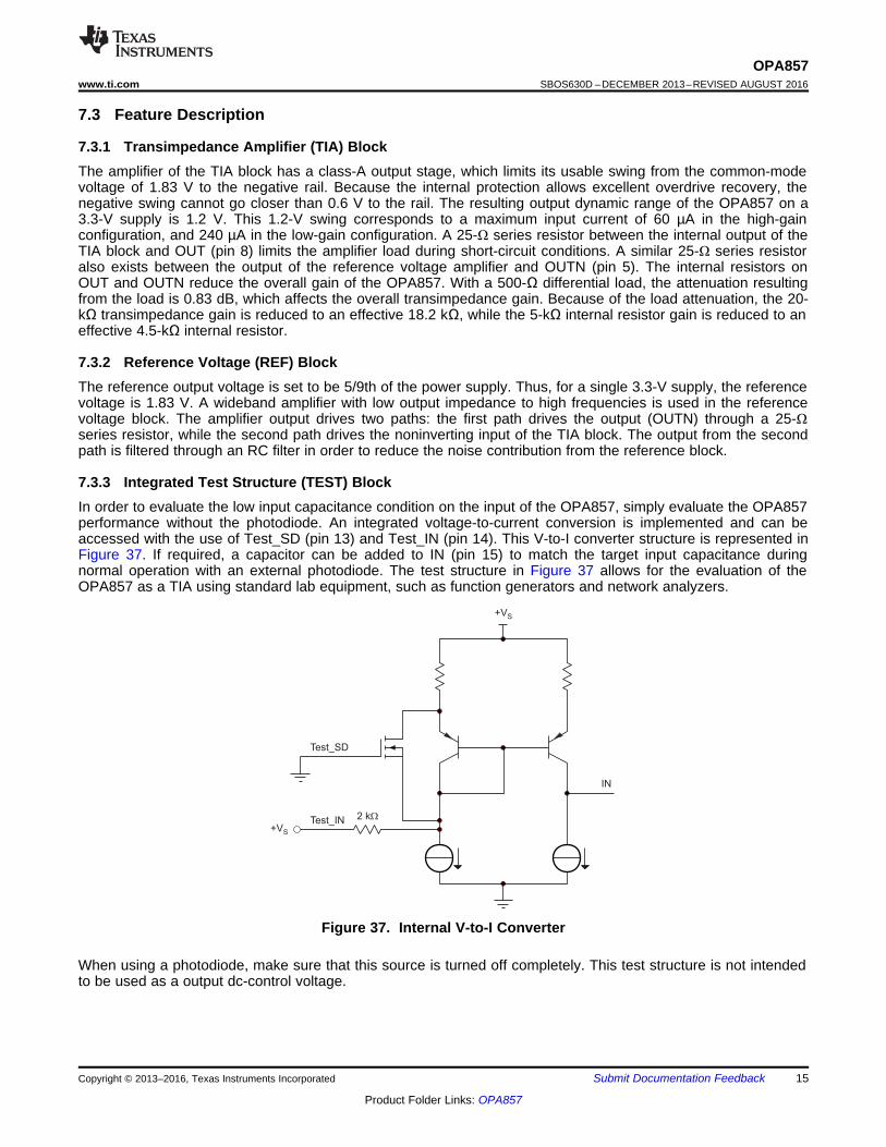
7.3.3 Integrated Test Structure (TEST) BlockIn order to evaluate the low input capacitance condition on the input of the OPA857, simply evaluate the OPA857performance without the photodiode. An integrated voltage-to-current conversion is implemented and can beaccessed with the use of Test_SD (pin 13) and Test_IN (pin 14). This V-to-I converter structure is represented inFigure 37. If required, a capacitor can be added to IN (pin 15) to match the target input capacitance duringnormal operation with an external photodiode. The test structure in Figure 37 allows for the evaluation of theOPA857 as a TIA using standard lab equipment, such as function generators and network analyzers.
Figure 37. Internal V-to-I Converter
When using a photodiode, make sure that this source is turned off completely. This test structure is not intendedto be used as a output dc-control voltage.

ExternalPin
+VCC
−VCC
InternalCircuitry
16
OPA857SBOS630D –DECEMBER 2013–REVISED AUGUST 2016 www.ti.com
Product Folder Links: OPA857
Submit Documentation Feedback Copyright © 2013–2016, Texas Instruments Incorporated
Feature Description (continued)
(1) Stresses beyond those listed under absolute maximum ratings may cause permanent damage to the device. These are stress ratingsonly, and functional operation of the device at these or any other conditions beyond those indicated under recommended operatingconditions is not implied. Exposure to absolute-maximum-rated conditions for extended periods may affect device reliability.
7.3.4 Internal Clamping Circuit (CLAMP) BlockThe OPA857 is built using a very high-speed, complementary, BICMOS process. The internal junctionbreakdown voltages are relatively low for these very small geometry devices. These breakdowns are reflected inthe Absolute Maximum Ratings (1) table. All device pins are protected with internal ESD protection diodes to thepower supplies, as shown in Figure 38.
Figure 38. Internal ESD Protection
These diodes provide moderate protection to input overdrive voltages above the supplies as well. The protectiondiodes can typically support 30-mA continuous current. Use additional external low-capacitance protection wherehigher currents are possible.

17
OPA857www.ti.com SBOS630D –DECEMBER 2013–REVISED AUGUST 2016
Product Folder Links: OPA857
Submit Documentation FeedbackCopyright © 2013–2016, Texas Instruments Incorporated
7.4 Device Functional Modes
7.4.1 Gain ControlThe device transimpedance gain is controlled with the CTRL pin. Setting the CTRL pin high results in selectingthe high-gain configuration. Setting the CTRL pin low results in selecting the low-gain configuration, as describedin Table 1.
Table 1. Gain Control Logic TableGAIN CTRL (Pin 2)5 kΩ Logic 0 (GND)
20 kΩ Logic 1 (+VS)
7.4.2 Test ModeThe OPA857 operates in normal mode when the input is driven by a photodiode. In test mode, the test structuredescribed in the Integrated Test Structure (TEST) Block section is used to emulate a photodiode using a voltageinput. Table 2 describes how to configure the OPA857 in each mode.
Table 2. Mode ConfigurationMODE Test_IN PIN CONNECTED TO Test_SD PIN CONNECTED TO
Normal mode +VS GND
Test mode AC-coupled input using a series cap ordc-coupled signal on a 2.1-V (approx) offset voltage +VS
Set an adequate dc voltage at the input to make sure that the output is operating within normal operation. Atminimum, the output of the TIA block must be set to 5/9th of the supply voltage in preparation for a pulseconfiguration. For sine-wave operation, as required when measuring a frequency response, set the dc voltage onthe OUT pin to allow the full sine-wave amplitude and avoid clipping. In such a case, the OUT pin voltage is setlower than 5/9th of the supply voltage.
Note that the 2-kΩ internal resistance used for the V-to-I conversion is not trimmed and can vary ±15% withprocess. Therefore, the source must be capable of sourcing both dc and ac voltages to make sure that the outputvoltage swing is compliant with the class-A output stage of the TIA block. Any change in the test circuitconfiguration (such as gain change) requires a new calibration of the internal V-to-I converter.
Again if a photodiode is used, the internal V-to-I converter must be shut off completely. Failure to do so results indegraded performance and higher than normal quiescent current.

+
±
+
±
VBIAS
Bias Reference
OPA857374
374
2 k
2 k
ADC34J45
50
50 1 k
1 k
VREF
THS4541 Clocking + FPGA+ Memory
18
OPA857SBOS630D –DECEMBER 2013–REVISED AUGUST 2016 www.ti.com
Product Folder Links: OPA857
Submit Documentation Feedback Copyright © 2013–2016, Texas Instruments Incorporated
8 Application and Implementation
NOTEInformation in the following applications sections is not part of the TI componentspecification, and TI does not warrant its accuracy or completeness. TI’s customers areresponsible for determining suitability of components for their purposes. Customers shouldvalidate and test their design implementation to confirm system functionality.
8.1 Application InformationThe OPA857 is a transimpedance amplifier offering two selectable gains. This device is used in conjunction witha photodiode at its input. The output is pseudo differential and may or may not require the use of a fullydifferential amplifier, depending on the analog-to-digital converter (ADC) used for implementation.
The OPA857 requires a photodiode to be connected to the positive bias voltage because the output voltage canonly swing down from the reference voltage (1.85 V for a 3.3-V supply) to ground.
8.2 Typical Application
8.2.1 TIA With Associated Signal ChainFigure 39 presents a complete end-to-end receive signal chain for an optical input. It includes a high-speedphotodiode, the OPA857, a THS4541 fully-differential amplifier, and a 16-bit, 160-MSPS, high-speed ADC. Forthe complete wide-bandwidth, optical front-end reference design, go to http://www.ti.com/tool/TIDA-00725.
Figure 39. TIA With Associated Signal Chain

19
OPA857www.ti.com SBOS630D –DECEMBER 2013–REVISED AUGUST 2016
Product Folder Links: OPA857
Submit Documentation FeedbackCopyright © 2013–2016, Texas Instruments Incorporated
Typical Application (continued)8.2.1.1 Design RequirementsFor this example, use the values listed in Table 3 for the input parameters.
Table 3. Design ParametersDESIGN PARAMETER EXAMPLE VALUE
Supply voltage 5-V external supplyAnalog bandwidth 120 MHzADC sampling rate 160 MSPS
Maximum system gain 100 kΩProgrammable transimpedance gain 5 kΩ / 20 kΩ
Maximum signal swing 1 VPP
Noise performance ≥ 60-dB SNRAveraged noise performance < 10-µVRMS
8.2.1.2 Detailed Design Procedure1. Use a high-speed, low input capacitance photodiode, such as the NR7500 or NR8300, as the front-end
optical sensor. Take care during layout to minimize parasitic capacitance added because of the PCB.2. Bias the photodiode with the cathode connected to a positive supply, and the anode connected to IN pin of
the OPA857. These connections make sure that the photodiode sources an output current that results in theOPA857 output swinging down below the reference voltage = (5 / 9) × 3.3 V = 1.83 V.
3. Disable the OPA857 test mode by setting Test_IN = +VS and Test_SD = GND. The transimpedance gain isselected by setting CTRL = +VS (gain = 20 kΩ) or CTRL = GND (gain = 5 kΩ).
4. The THS4541 is configured in a gain of 5 V/V in order to achieve a maximum signal transimpedance gain of100 kΩ. It is important to carefully select the value of the RG gain resistors for the THS4541.
5. Setting RG very low increases the resistive loading on the previous OPA857 output stage, and reduces thebandwidth of the OPA857.
6. Setting RG very high results in a large value of feedback resistance, RF, on the THS4541 in order to achievethe desired 5V/V gain. RF interacts with the input capacitance of the THS4541 to create a zero in the noise-gain response of the amplifier, and if not properly compensated, results in reduced phase-margin andpotential instability.
7. A value of RG = 374 Ω was selected that results in a total differential load of 798 Ω on the OPA857. Theresultant RF = 2 kΩ.
8. The response to an optical pulsed input is shown in Figure 40 to Figure 43. To prevent signal reflectionsbetween the THS4541 output and the ADC34J45 input, the signal is doubly terminated through 50-Ωresistors. If the THS4541 and ADC34J45 are physically close together on the PCB, then the double-termination is eliminated, which increases the overall gain of the signal chain without affecting the transientresponse of the system. These results were verified, and the complete data is available in reference designTIDA-00725.
9. An optional antialiasing filter can be added between the THS4541 and the ADC34J45 to reduce systemnoise caused by aliasing.

Time (Ps)
Out
put V
olta
ge (
V)
0 0.25 0.5 0.75 1 1.25 1.5 1.75 2 2.25 2.5 2.75 3 3.25 3.5 3.75 410P
100P
1m
10m
100m
1
D006
125 mV250 mV500 mV950 mV
Time (Ps)
Out
put V
olta
ge (
V)
0 1 2 3 4 5 6 7 8 9 10
D007
-50P
0P
50P
100P
150P
200P
250P
300P
350P
400P125 mV250 mV500 mV1 V
Time (Ps)
Out
put V
olta
ge (
V)
0 0.25 0.5 0.75 1 1.25 1.5 1.75 2 2.25 2.5 2.75 3 3.25 3.5 3.75 410P
100P
1m
10m
100m
1
D004
125 mV250 mV500 mV950 mV
Time (Ps)
Out
put V
olta
ge (
V)
0 1 2 3 4 5 6 7 8 9 10
D005
0
-50P
50P
100P
150P
200P
250P
300P
350P
400P125 mV250 mV500 mV1 V
20
OPA857SBOS630D –DECEMBER 2013–REVISED AUGUST 2016 www.ti.com
Product Folder Links: OPA857
Submit Documentation Feedback Copyright © 2013–2016, Texas Instruments Incorporated
8.2.1.3 Application Curves
TZ Gain = 20 kΩ
Figure 40. Pulse Response vs Output Voltage
TZ Gain = 20 kΩ
Figure 41. Long-Term Settling Response vs OutputVoltage
TZ Gain = 5 kΩ
Figure 42. Pulse Response vs Output Voltage
TZ Gain = 5 kΩ
Figure 43. Long-Term Settling Response vs OutputVoltage

+
±RF1
RF2
TIA
IN
REFClamping
Cicuit
25
25
OUT
OUTN
CLAMP
1:12 k
TEST
Test_In
Test_SD
CTRL +VS GND
External RF
VBIAS
External CF
21
OPA857www.ti.com SBOS630D –DECEMBER 2013–REVISED AUGUST 2016
Product Folder Links: OPA857
Submit Documentation FeedbackCopyright © 2013–2016, Texas Instruments Incorporated
8.2.2 Extending Transimpedance BandwidthAt the core of the OPA857 is an ultrawide bandwidth op amp. One of the highlights of the OPA857 is therelatively small change in the transimpedance bandwidth as a function of the internal gain selected; 130 MHz(gain = 5 kΩ) and 105 MHz (gain = 20 kΩ). Theoretically, for a four times increase in gain, the bandwidth shouldreduce by two times; however, as observed in the case of the OPA857, the results do not follow theory. For moreinformation on the various factors that contribute to an amplifier frequency-response performance whenconfigured as a TIA, see What You Need To Know About Transimpedance Amplifiers – Part 1 on the TI E2ECommunity website at e2e.ti.com. This blog also contains a reference to an excel calculator to simplify TIAdesigns when using discrete opamps. The OPA857 is unique in displaying this type of behavior because theCTRL logic controls an internal switch in the amplifier core that recompensates the amplifier open-loop gaincharacteristic depending upon the logic level. In this application, it it shown how the closed-loop transimpedancebandwidth can be increased to greater than 250 MHz. The circuit used for this test is shown in Figure 44. Anexternal feedback resistor, RF, is added in parallel to the internal transimpedance gain resistors of the OPA857.This resistor has the effect of reducing the overall transimpedance gain, but with increased bandwidth.
Figure 44. Extending Transimpedance Bandwidth
8.2.2.1 Design RequirementsFor this example, use the values listed in Table 4 for the input parameters.
Table 4. Design ParametersDESIGN PARAMETER EXAMPLE VALUE
Supply voltage 3.3 VOutput swing 500 mVPP
Differential output load 500 kΩ and 1 kΩTarget bandwidth 250 MHz
Effective transimpedance gain 5 kΩ

Frequency (Hz)
Out
put (
dB)
-4
-3
-2
-1
0
1
2
3
4
1M 10M 100M 1G
D007
RF(Internal) = 20 k:, RF || CF(External) = 6.8 k: || 0.1 pFRF(Internal) = 5 k:, RF || CF(External) = 6.8 k: || 0.1 pF
Frequency (Hz)
Out
put (
dB)
-4
-3
-2
-1
0
1
2
3
4
1M 10M 100M 1G
D003
RF = 20 k: (Internal) || 6.8 k: (External)RF = 5 k: (Internal) || 6.8 k: (External)
Frequency (Hz)
Out
put (
dB)
-2
-1.5
-1
-0.5
0
0.5
1
1.5
2
1M 10M 100M
D004
RF(Internal) = 20 k:, RF || CF(External) = 6.8 k: || 0.1 pFRF(Internal) = 5 k:, RF || CF(External) = 6.8 k: || 0.1 pF
22
OPA857SBOS630D –DECEMBER 2013–REVISED AUGUST 2016 www.ti.com
Product Folder Links: OPA857
Submit Documentation Feedback Copyright © 2013–2016, Texas Instruments Incorporated
8.2.2.2 Application CurvesFigure 45 shows the frequency response with a feedback resistance of 6.8 kΩ and an output load of 500 Ω. Thelarge amount of peaking indicates a low phase-margin and potential instability. Next, a 0.1-pF feedbackcapacitor, CF, is added in parallel to the 6.8-kΩ RF. Both RF and CF interact to create pole in the noise gain curvethat counteracts the effect of the zero caused by RF, and the total input capacitance at pin IN of the OPA857.The input capacitance is caused by the opamps inherent input capacitance, the photodiode capacitance, and theparasitic input capacitance from the PCB. The pole zero cancellation increases the phase margin, as is evident inthe reduced peaking shown in Figure 46. In Figure 47, an output load of 1 kΩ was used, along with an RF = 6.8kΩ and CF = 0.1 pF. The reduced load helps to increase the op amp open-loop gain, which in turn increases theclosed-loop bandwidth of the OPA857 circuit.
RF = 6.8 kΩ
Figure 45. Frequency Response With External Feedback
RF = 6.8 kΩ, CF = 0.1 pF
Figure 46. Frequency Response With External Feedback
RF = 6.8 kΩ, CF = 0.1 pF
Figure 47. Frequency Response With External Feedback
23
OPA857www.ti.com SBOS630D –DECEMBER 2013–REVISED AUGUST 2016
Product Folder Links: OPA857
Submit Documentation FeedbackCopyright © 2013–2016, Texas Instruments Incorporated
9 Power-Supply RecommendationsUse a linear power supply with good PSRR. For a good, high-frequency, power-supply bypass, use a ceramiccapacitor connected as close as possible to the +VS pin.
10 Layout
10.1 Layout GuidelinesAchieving optimum performance with a high-frequency amplifier such as the OPA857 requires careful attention toboard layout parasitics and external component types. Recommendations that optimize performance include:a. Minimize parasitic capacitance to any ac ground for all signal I/O pins. Parasitic capacitance on the
inverting input pin can cause instability. To reduce unwanted capacitance, open a window around the signalI/O pins in all ground and power planes around those pins. Otherwise, make sure that ground and powerplanes are unbroken elsewhere on the board.
b. Minimize the distance (< 0.25") from the power-supply pins to high-frequency 0.1-µF decoupling capacitors,as shown in Figure 48. At the device pins, make sure that the ground and power-plane layout are not inclose proximity to the signal I/O pins. Avoid narrow power and ground traces to minimize inductance betweenthe pins and decoupling capacitors. Always decouple the power-supply connections with these capacitors.An optional supply decoupling capacitor (0.1 µF) across the two power supplies (for bipolar operation)improves second-harmonic distortion performance. Use larger (2.2 µF to 6.8 µF) decoupling capacitors,effective at lower frequencies, on the main supply pins. These capacitors can be placed somewhat fartherfrom the device and can be shared among several devices in the same area of the PC board.
c. Careful selection and placement of external components preserves the high-frequency performanceof the OPA857. Use very low reactance type resistors. Surface-mount resistors function best and allow atighter overall layout. Metal-film or carbon composition, axially-leaded resistors also provide good high-frequency performance. Again, keep the leads and PC board traces as short as possible. Never usewirewound type resistors in a high-frequency application.
d. Connections to other wideband devices on the board can be made with short, direct traces or throughonboard transmission lines. For short connections, consider the trace and the input to the next device as alumped capacitive load. Use relatively wide traces (50 mils to 100 mils), preferably with ground and powerplanes opened up around them.
e. Do not socket a high-speed part such as the OPA857. The additional lead length and pin-to-pincapacitance introduced by the socket can create an extremely troublesome parasitic network that makesachieving a smooth, stable frequency response almost impossible. Best results are obtained by soldering theOPA857 onto the board.

10-nFBypass Capacitor
C2 and C3as Close as Possibleto +Vs and GND Pins
OUT
GND
GND
OUTN
Test_SD
Test_IN
IN
NC
CT
RL
Open Planes to Minimize Parasitic Input Capacitance
100-nFBypass Capacitor
< 0.25"
24
OPA857SBOS630D –DECEMBER 2013–REVISED AUGUST 2016 www.ti.com
Product Folder Links: OPA857
Submit Documentation Feedback Copyright © 2013–2016, Texas Instruments Incorporated
10.2 Layout Example
Figure 48. Layout Example

25
OPA857www.ti.com SBOS630D –DECEMBER 2013–REVISED AUGUST 2016
Product Folder Links: OPA857
Submit Documentation FeedbackCopyright © 2013–2016, Texas Instruments Incorporated
11 Device and Documentation Support
11.1 Device Support
11.1.1 Development Support
11.1.1.1 Evaluation ModuleAn evaluation module (EVM) is available to assist in the initial circuit performance evaluation using the OPA857.The summary information for this fixture is shown in Table 5.
Table 5. EVM Ordering InformationPRODUCT PACKAGE ORDERING NUMBER LITERATURE NUMBER
OPA857IRGT RGT OPA857EVM SBOU138
The EVM can be requested at the Texas Instruments web site (www.ti.com) through the OPA857 product folder.
11.1.1.2 Spice ModelComputer simulation of circuit performance using spice is often useful when analyzing the performance of analogcircuits and systems. The previous statement is particularly true for transimpedance applications where parasiticcapacitance and inductance can have a major effect on circuit performance. A spice model for the OPA857 isavailable through the OPA857 product folder under simulation models. These models do a good job of predictingsmall-signal ac and transient performance under a wide variety of operating conditions. These models, however,do not do as well in predicting harmonic distortion.
11.2 Documentation Support
11.2.1 Related DocumentationFor related documentation, see the following:• OPA857EVM Evaluation Module (SBOU138)• Transimpedance Considerations for High-speed Amplifiers (SBOA122)• Wide Bandwidth Optical Front-end Reference Design (TIDUAZ1)• Reference Design for Extending the OPA857 Transimpedance Bandwidth (TIDUBX7)• Learn how to compensate transimpedance amplifiers intuitively in:
What You Need To Know About Transimpedance Amplifiers – Part 1 (Cherian 2016)
11.3 Receiving Notification of Documentation UpdatesTo receive notification of documentation updates, navigate to the device product folder on ti.com. In the upperright corner, click on Alert me to register and receive a weekly digest of any product information that haschanged. For change details, review the revision history included in any revised document.
11.4 Community ResourcesThe following links connect to TI community resources. Linked contents are provided "AS IS" by the respectivecontributors. They do not constitute TI specifications and do not necessarily reflect TI's views; see TI's Terms ofUse.
TI E2E™ Online Community TI's Engineer-to-Engineer (E2E) Community. Created to foster collaborationamong engineers. At e2e.ti.com, you can ask questions, share knowledge, explore ideas and helpsolve problems with fellow engineers.
Design Support TI's Design Support Quickly find helpful E2E forums along with design support tools andcontact information for technical support.
11.5 TrademarksE2E is a trademark of Texas Instruments.All other trademarks are the property of their respective owners.
26
OPA857SBOS630D –DECEMBER 2013–REVISED AUGUST 2016 www.ti.com
Product Folder Links: OPA857
Submit Documentation Feedback Copyright © 2013–2016, Texas Instruments Incorporated
11.6 Electrostatic Discharge CautionThis integrated circuit can be damaged by ESD. Texas Instruments recommends that all integrated circuits be handled withappropriate precautions. Failure to observe proper handling and installation procedures can cause damage.
ESD damage can range from subtle performance degradation to complete device failure. Precision integrated circuits may be moresusceptible to damage because very small parametric changes could cause the device not to meet its published specifications.
11.7 GlossarySLYZ022 — TI Glossary.
This glossary lists and explains terms, acronyms, and definitions.
12 Mechanical, Packaging, and Orderable InformationThe following pages include mechanical packaging and orderable information. This information is the mostcurrent data available for the designated devices. This data is subject to change without notice and revision ofthis document. For browser-based versions of this data sheet, refer to the left-hand navigation.

PACKAGE OPTION ADDENDUM
www.ti.com 11-Aug-2017
Addendum-Page 1
PACKAGING INFORMATION
Orderable Device Status(1)
Package Type PackageDrawing
Pins PackageQty
Eco Plan(2)
Lead/Ball Finish(6)
MSL Peak Temp(3)
Op Temp (°C) Device Marking(4/5)
Samples
OPA857IRGTR ACTIVE VQFN RGT 16 3000 Green (RoHS& no Sb/Br)
CU NIPDAU Level-2-260C-1 YEAR -40 to 95 OPA857
OPA857IRGTT ACTIVE VQFN RGT 16 250 Green (RoHS& no Sb/Br)
CU NIPDAU Level-2-260C-1 YEAR -40 to 95 OPA857
(1) The marketing status values are defined as follows:ACTIVE: Product device recommended for new designs.LIFEBUY: TI has announced that the device will be discontinued, and a lifetime-buy period is in effect.NRND: Not recommended for new designs. Device is in production to support existing customers, but TI does not recommend using this part in a new design.PREVIEW: Device has been announced but is not in production. Samples may or may not be available.OBSOLETE: TI has discontinued the production of the device.
(2) RoHS: TI defines "RoHS" to mean semiconductor products that are compliant with the current EU RoHS requirements for all 10 RoHS substances, including the requirement that RoHS substancedo not exceed 0.1% by weight in homogeneous materials. Where designed to be soldered at high temperatures, "RoHS" products are suitable for use in specified lead-free processes. TI mayreference these types of products as "Pb-Free".RoHS Exempt: TI defines "RoHS Exempt" to mean products that contain lead but are compliant with EU RoHS pursuant to a specific EU RoHS exemption.Green: TI defines "Green" to mean the content of Chlorine (Cl) and Bromine (Br) based flame retardants meet JS709B low halogen requirements of <=1000ppm threshold. Antimony trioxide basedflame retardants must also meet the <=1000ppm threshold requirement.
(3) MSL, Peak Temp. - The Moisture Sensitivity Level rating according to the JEDEC industry standard classifications, and peak solder temperature.
(4) There may be additional marking, which relates to the logo, the lot trace code information, or the environmental category on the device.
(5) Multiple Device Markings will be inside parentheses. Only one Device Marking contained in parentheses and separated by a "~" will appear on a device. If a line is indented then it is a continuationof the previous line and the two combined represent the entire Device Marking for that device.
(6) Lead/Ball Finish - Orderable Devices may have multiple material finish options. Finish options are separated by a vertical ruled line. Lead/Ball Finish values may wrap to two lines if the finishvalue exceeds the maximum column width.
Important Information and Disclaimer:The information provided on this page represents TI's knowledge and belief as of the date that it is provided. TI bases its knowledge and belief on informationprovided by third parties, and makes no representation or warranty as to the accuracy of such information. Efforts are underway to better integrate information from third parties. TI has taken andcontinues to take reasonable steps to provide representative and accurate information but may not have conducted destructive testing or chemical analysis on incoming materials and chemicals.TI and TI suppliers consider certain information to be proprietary, and thus CAS numbers and other limited information may not be available for release.
In no event shall TI's liability arising out of such information exceed the total purchase price of the TI part(s) at issue in this document sold by TI to Customer on an annual basis.

PACKAGE OPTION ADDENDUM
www.ti.com 11-Aug-2017
Addendum-Page 2

TAPE AND REEL INFORMATION
*All dimensions are nominal
Device PackageType
PackageDrawing
Pins SPQ ReelDiameter
(mm)
ReelWidth
W1 (mm)
A0(mm)
B0(mm)
K0(mm)
P1(mm)
W(mm)
Pin1Quadrant
OPA857IRGTR VQFN RGT 16 3000 330.0 12.4 3.3 3.3 1.1 8.0 12.0 Q2
OPA857IRGTT VQFN RGT 16 250 180.0 12.4 3.3 3.3 1.1 8.0 12.0 Q2
PACKAGE MATERIALS INFORMATION
www.ti.com 11-Aug-2017
Pack Materials-Page 1

*All dimensions are nominal
Device Package Type Package Drawing Pins SPQ Length (mm) Width (mm) Height (mm)
OPA857IRGTR VQFN RGT 16 3000 367.0 367.0 35.0
OPA857IRGTT VQFN RGT 16 250 210.0 185.0 35.0
PACKAGE MATERIALS INFORMATION
www.ti.com 11-Aug-2017
Pack Materials-Page 2


www.ti.com
PACKAGE OUTLINE
C
16X 0.300.18
1.45 0.1
16X 0.50.3
1 MAX
(0.2) TYP
0.050.00
12X 0.5
4X1.5
A 3.12.9
B
3.12.9
VQFN - 1 mm max heightRGT0016APLASTIC QUAD FLATPACK - NO LEAD
4219032/A 02/2017
PIN 1 INDEX AREA
0.08
SEATING PLANE
1
49
12
5 8
16 13
(OPTIONAL)PIN 1 ID 0.1 C A B
0.05
EXPOSEDTHERMAL PAD
SYMM
SYMM
17
NOTES: 1. All linear dimensions are in millimeters. Any dimensions in parenthesis are for reference only. Dimensioning and tolerancing per ASME Y14.5M. 2. This drawing is subject to change without notice. 3. The package thermal pad must be soldered to the printed circuit board for thermal and mechanical performance.4. Reference JEDEC registration MO-220
SCALE 3.600
www.ti.com
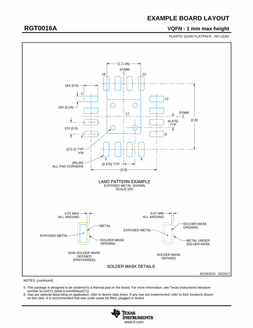
EXAMPLE BOARD LAYOUT
0.07 MINALL AROUND
0.07 MAXALL AROUND
16X (0.24)
16X (0.6)
( 0.2) TYPVIA
12X (0.5)
(2.8)
(2.8)
(0.475)TYP
( 1.45)
(R0.05)ALL PAD CORNERS
(0.475) TYP
VQFN - 1 mm max heightRGT0016APLASTIC QUAD FLATPACK - NO LEAD
4219032/A 02/2017
SYMM
1
4
5 8
9
12
1316
SYMM
LAND PATTERN EXAMPLEEXPOSED METAL SHOWN
SCALE:20X
17
NOTES: (continued) 5. This package is designed to be soldered to a thermal pad on the board. For more information, see Texas Instruments literature number SLUA271 (www.ti.com/lit/slua271).6. Vias are optional depending on application, refer to device data sheet. If any vias are implemented, refer to their locations shown on this view. It is recommended that vias under paste be filled, plugged or tented.
SOLDER MASKOPENING
METAL UNDERSOLDER MASK
SOLDER MASKDEFINED
EXPOSED METALMETAL
SOLDER MASKOPENING
SOLDER MASK DETAILS
NON SOLDER MASKDEFINED
(PREFERRED)
EXPOSED METAL
www.ti.com
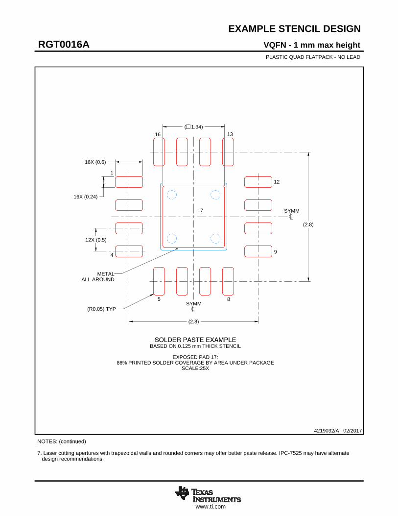
EXAMPLE STENCIL DESIGN
16X (0.6)
16X (0.24)
12X (0.5)
(2.8)
(2.8)
( 1.34)
(R0.05) TYP
VQFN - 1 mm max heightRGT0016APLASTIC QUAD FLATPACK - NO LEAD
4219032/A 02/2017
NOTES: (continued) 7. Laser cutting apertures with trapezoidal walls and rounded corners may offer better paste release. IPC-7525 may have alternate design recommendations.
SYMM
ALL AROUNDMETAL
SOLDER PASTE EXAMPLEBASED ON 0.125 mm THICK STENCIL
EXPOSED PAD 17:
86% PRINTED SOLDER COVERAGE BY AREA UNDER PACKAGESCALE:25X
SYMM
1
4
5 8
9
12
1316
17

IMPORTANT NOTICE
Texas Instruments Incorporated (TI) reserves the right to make corrections, enhancements, improvements and other changes to itssemiconductor products and services per JESD46, latest issue, and to discontinue any product or service per JESD48, latest issue. Buyersshould obtain the latest relevant information before placing orders and should verify that such information is current and complete.TI’s published terms of sale for semiconductor products (http://www.ti.com/sc/docs/stdterms.htm) apply to the sale of packaged integratedcircuit products that TI has qualified and released to market. Additional terms may apply to the use or sale of other types of TI products andservices.Reproduction of significant portions of TI information in TI data sheets is permissible only if reproduction is without alteration and isaccompanied by all associated warranties, conditions, limitations, and notices. TI is not responsible or liable for such reproduceddocumentation. Information of third parties may be subject to additional restrictions. Resale of TI products or services with statementsdifferent from or beyond the parameters stated by TI for that product or service voids all express and any implied warranties for theassociated TI product or service and is an unfair and deceptive business practice. TI is not responsible or liable for any such statements.Buyers and others who are developing systems that incorporate TI products (collectively, “Designers”) understand and agree that Designersremain responsible for using their independent analysis, evaluation and judgment in designing their applications and that Designers havefull and exclusive responsibility to assure the safety of Designers' applications and compliance of their applications (and of all TI productsused in or for Designers’ applications) with all applicable regulations, laws and other applicable requirements. Designer represents that, withrespect to their applications, Designer has all the necessary expertise to create and implement safeguards that (1) anticipate dangerousconsequences of failures, (2) monitor failures and their consequences, and (3) lessen the likelihood of failures that might cause harm andtake appropriate actions. Designer agrees that prior to using or distributing any applications that include TI products, Designer willthoroughly test such applications and the functionality of such TI products as used in such applications.TI’s provision of technical, application or other design advice, quality characterization, reliability data or other services or information,including, but not limited to, reference designs and materials relating to evaluation modules, (collectively, “TI Resources”) are intended toassist designers who are developing applications that incorporate TI products; by downloading, accessing or using TI Resources in anyway, Designer (individually or, if Designer is acting on behalf of a company, Designer’s company) agrees to use any particular TI Resourcesolely for this purpose and subject to the terms of this Notice.TI’s provision of TI Resources does not expand or otherwise alter TI’s applicable published warranties or warranty disclaimers for TIproducts, and no additional obligations or liabilities arise from TI providing such TI Resources. TI reserves the right to make corrections,enhancements, improvements and other changes to its TI Resources. TI has not conducted any testing other than that specificallydescribed in the published documentation for a particular TI Resource.Designer is authorized to use, copy and modify any individual TI Resource only in connection with the development of applications thatinclude the TI product(s) identified in such TI Resource. NO OTHER LICENSE, EXPRESS OR IMPLIED, BY ESTOPPEL OR OTHERWISETO ANY OTHER TI INTELLECTUAL PROPERTY RIGHT, AND NO LICENSE TO ANY TECHNOLOGY OR INTELLECTUAL PROPERTYRIGHT OF TI OR ANY THIRD PARTY IS GRANTED HEREIN, including but not limited to any patent right, copyright, mask work right, orother intellectual property right relating to any combination, machine, or process in which TI products or services are used. Informationregarding or referencing third-party products or services does not constitute a license to use such products or services, or a warranty orendorsement thereof. Use of TI Resources may require a license from a third party under the patents or other intellectual property of thethird party, or a license from TI under the patents or other intellectual property of TI.TI RESOURCES ARE PROVIDED “AS IS” AND WITH ALL FAULTS. TI DISCLAIMS ALL OTHER WARRANTIES ORREPRESENTATIONS, EXPRESS OR IMPLIED, REGARDING RESOURCES OR USE THEREOF, INCLUDING BUT NOT LIMITED TOACCURACY OR COMPLETENESS, TITLE, ANY EPIDEMIC FAILURE WARRANTY AND ANY IMPLIED WARRANTIES OFMERCHANTABILITY, FITNESS FOR A PARTICULAR PURPOSE, AND NON-INFRINGEMENT OF ANY THIRD PARTY INTELLECTUALPROPERTY RIGHTS. TI SHALL NOT BE LIABLE FOR AND SHALL NOT DEFEND OR INDEMNIFY DESIGNER AGAINST ANY CLAIM,INCLUDING BUT NOT LIMITED TO ANY INFRINGEMENT CLAIM THAT RELATES TO OR IS BASED ON ANY COMBINATION OFPRODUCTS EVEN IF DESCRIBED IN TI RESOURCES OR OTHERWISE. IN NO EVENT SHALL TI BE LIABLE FOR ANY ACTUAL,DIRECT, SPECIAL, COLLATERAL, INDIRECT, PUNITIVE, INCIDENTAL, CONSEQUENTIAL OR EXEMPLARY DAMAGES INCONNECTION WITH OR ARISING OUT OF TI RESOURCES OR USE THEREOF, AND REGARDLESS OF WHETHER TI HAS BEENADVISED OF THE POSSIBILITY OF SUCH DAMAGES.Unless TI has explicitly designated an individual product as meeting the requirements of a particular industry standard (e.g., ISO/TS 16949and ISO 26262), TI is not responsible for any failure to meet such industry standard requirements.Where TI specifically promotes products as facilitating functional safety or as compliant with industry functional safety standards, suchproducts are intended to help enable customers to design and create their own applications that meet applicable functional safety standardsand requirements. Using products in an application does not by itself establish any safety features in the application. Designers mustensure compliance with safety-related requirements and standards applicable to their applications. Designer may not use any TI products inlife-critical medical equipment unless authorized officers of the parties have executed a special contract specifically governing such use.Life-critical medical equipment is medical equipment where failure of such equipment would cause serious bodily injury or death (e.g., lifesupport, pacemakers, defibrillators, heart pumps, neurostimulators, and implantables). Such equipment includes, without limitation, allmedical devices identified by the U.S. Food and Drug Administration as Class III devices and equivalent classifications outside the U.S.TI may expressly designate certain products as completing a particular qualification (e.g., Q100, Military Grade, or Enhanced Product).Designers agree that it has the necessary expertise to select the product with the appropriate qualification designation for their applicationsand that proper product selection is at Designers’ own risk. Designers are solely responsible for compliance with all legal and regulatoryrequirements in connection with such selection.Designer will fully indemnify TI and its representatives against any damages, costs, losses, and/or liabilities arising out of Designer’s non-compliance with the terms and provisions of this Notice.
Mailing Address: Texas Instruments, Post Office Box 655303, Dallas, Texas 75265Copyright © 2017, Texas Instruments Incorporated


![NJU8759A600 800 1000 1200 1400 1600 1800 2000 0 25 50 75 100 125 消費電 力 P D [m W 周囲温度[ C] せヴむゐずヴょぇあゐな 2-Layer 4-Layer TON TOFF STBYB OUTP/OUTN](https://static.fdocuments.net/doc/165x107/60ac6729484cfa1396440950/nju8759a-600-800-1000-1200-1400-1600-1800-2000-0-25-50-75-100-125-ee-.jpg)