“Op-Amp” Operational Amplifier Non Inverting Amplifier Inverting Amplifier Adder –(and...
40
“Op-Amp” Operational Amplifier • Non Inverting Amplifier • Inverting Amplifier • Adder – (and Subtractor using an Inverter) • Differential Amplifier • Integrator • Differentiator Op-Amp name derives from early usage of these elements in performing mathematical operations in analog computers.
-
Upload
giles-washington -
Category
Documents
-
view
344 -
download
6
Transcript of “Op-Amp” Operational Amplifier Non Inverting Amplifier Inverting Amplifier Adder –(and...

“Op-Amp”Operational Amplifier
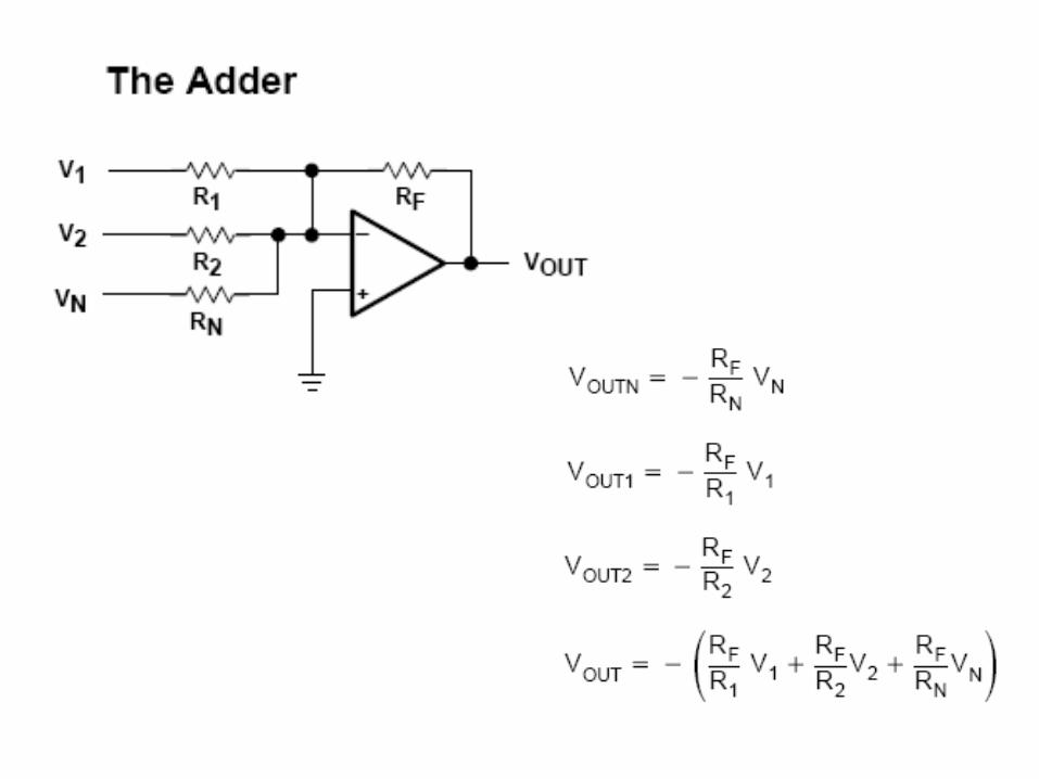
• Non Inverting Amplifier• Inverting Amplifier• Adder
– (and Subtractor using an Inverter)
• Differential Amplifier• Integrator• Differentiator
Op-Amp name derives from early usage of these elements in performing mathematical operations in analog computers.
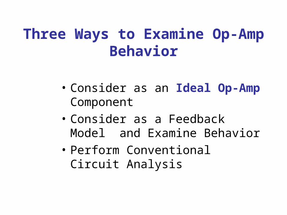
Three Ways to Examine Op-Amp Behavior
• Consider as an Ideal Op-Amp Component
• Consider as a Feedback Model and Examine Behavior
• Perform Conventional Circuit Analysis
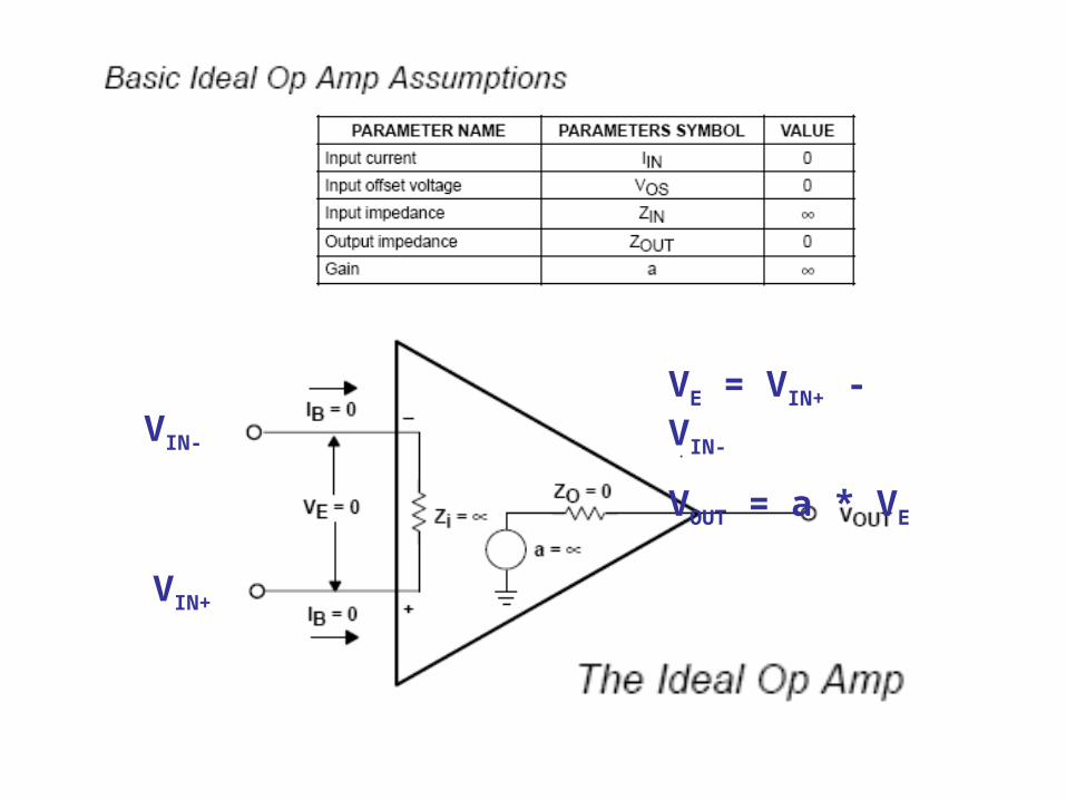
VE = VIN+ - VIN-
VOUT = a * VE
VIN+
VIN-
Ideal Op-Amp Model
VE = VIN+ - VIN-
VOUT = a * VE
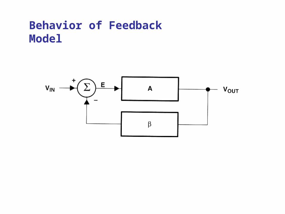
Behavior of Feedback Model
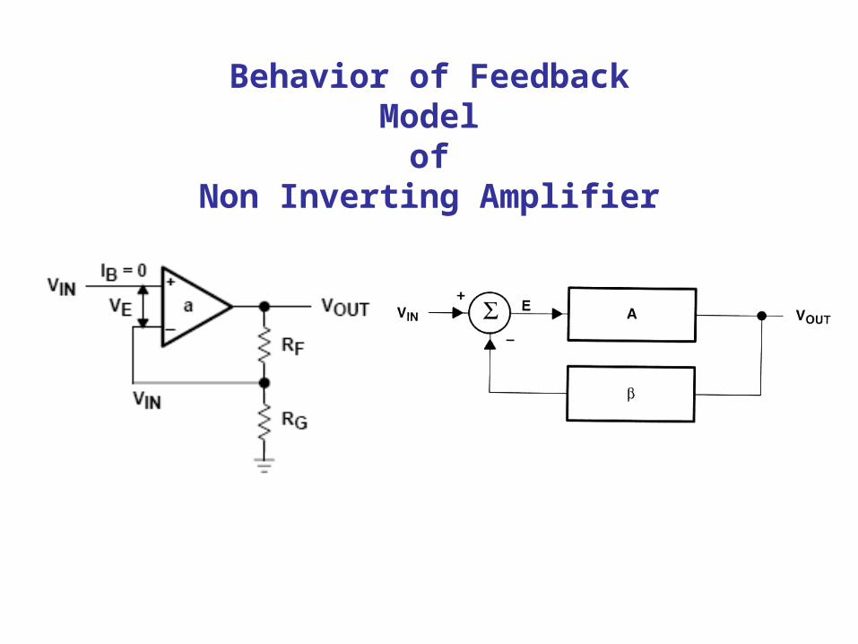
Behavior of Feedback Modelof
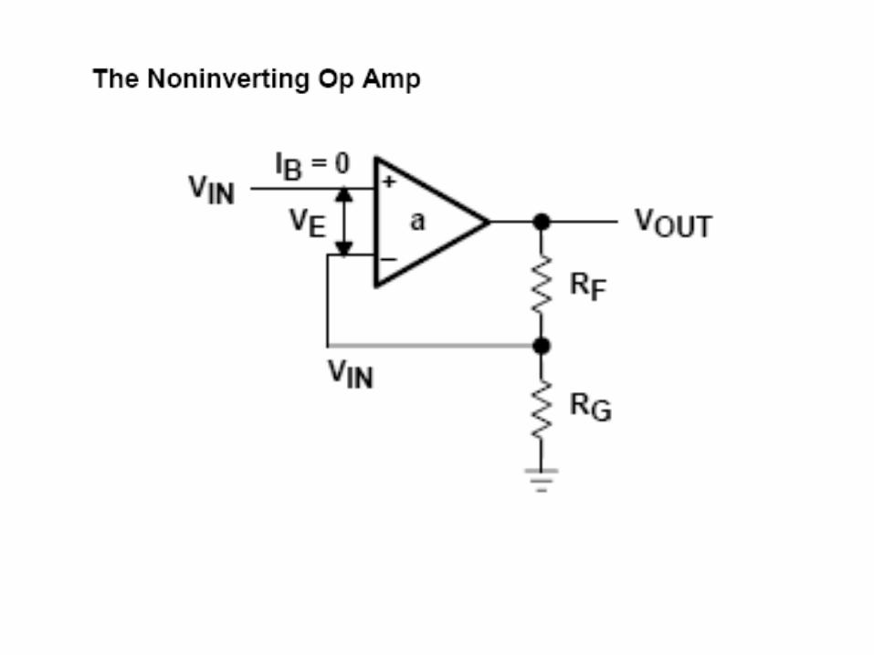
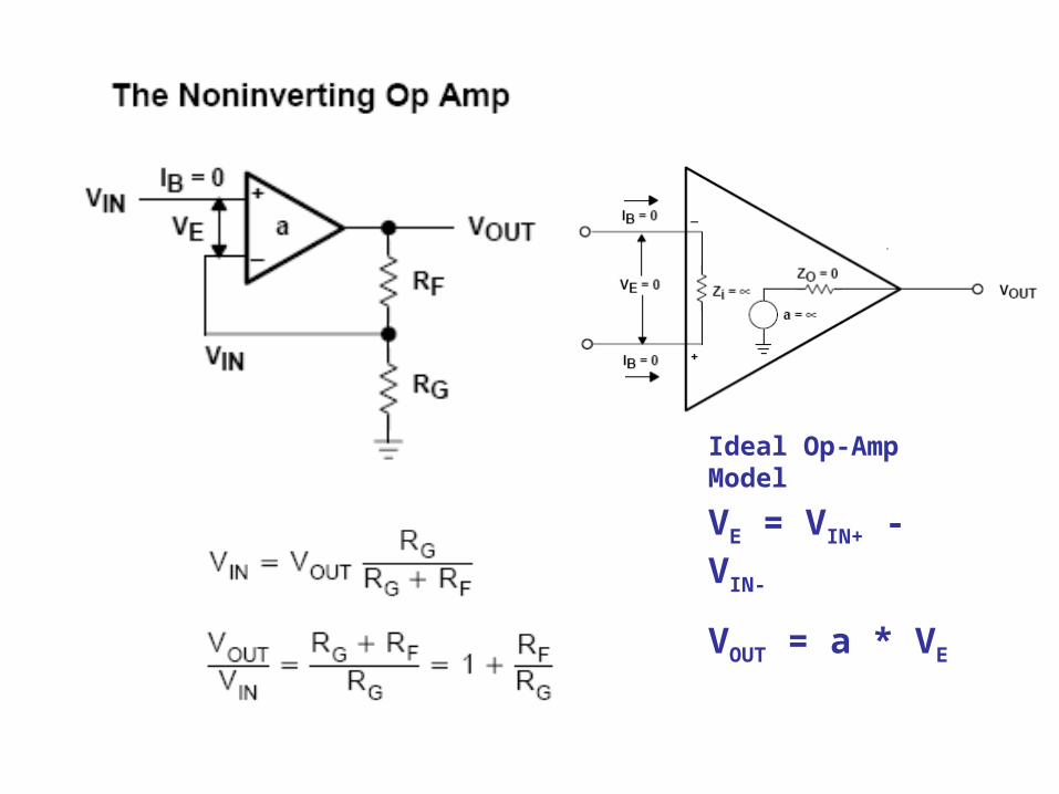
Non Inverting Amplifier
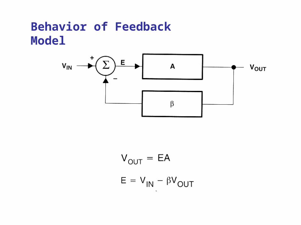
Behavior of Feedback Model
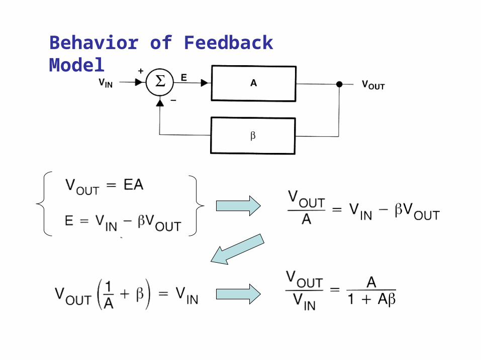
Behavior of Feedback Model
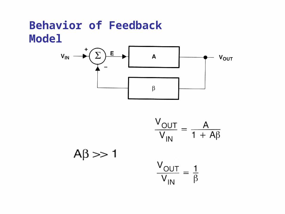
Behavior of Feedback Model
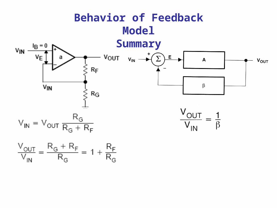
Behavior of Feedback ModelSummary
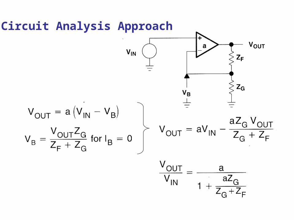
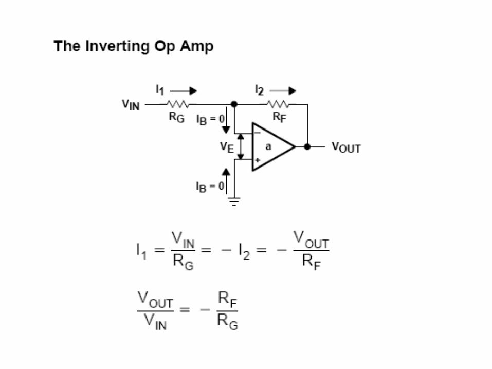
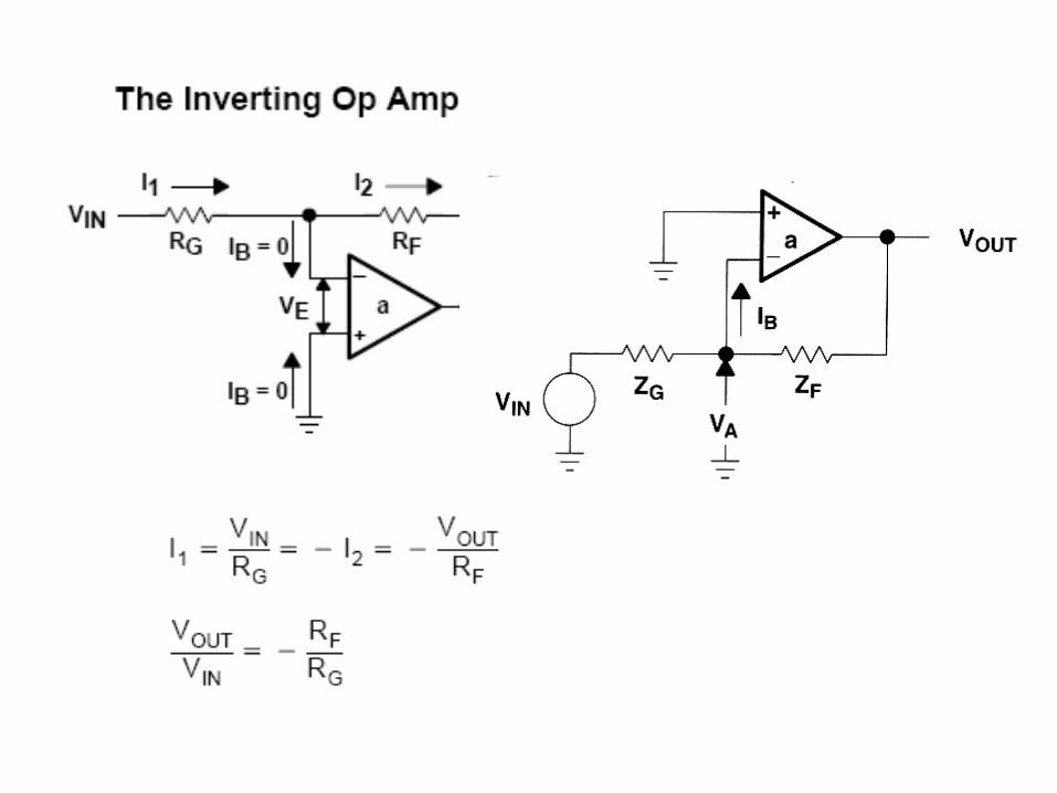
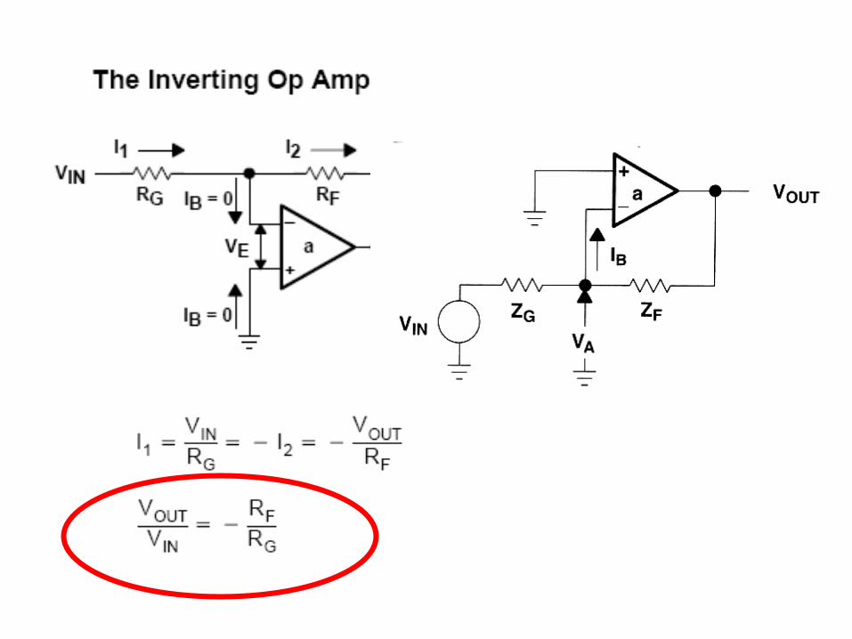
Circuit Analysis Approach
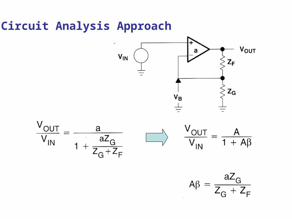
Circuit Analysis Approach
“Op-Amp”Operational Amplifier
• Non Inverting Amplifier• Inverting Amplifier• Adder
– (and Subtractor using an Inverter)
• Differential Amplifier• Integrator• Differentiator
Op-Amp name derives from early usage of these elements in performing mathematical operations in analog computers.
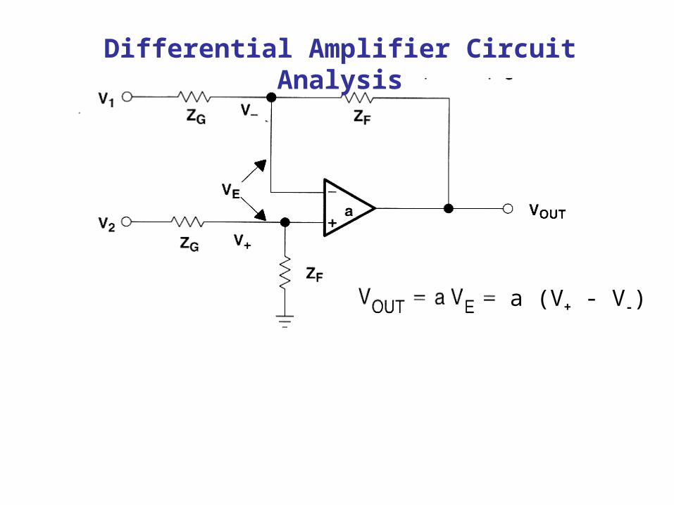
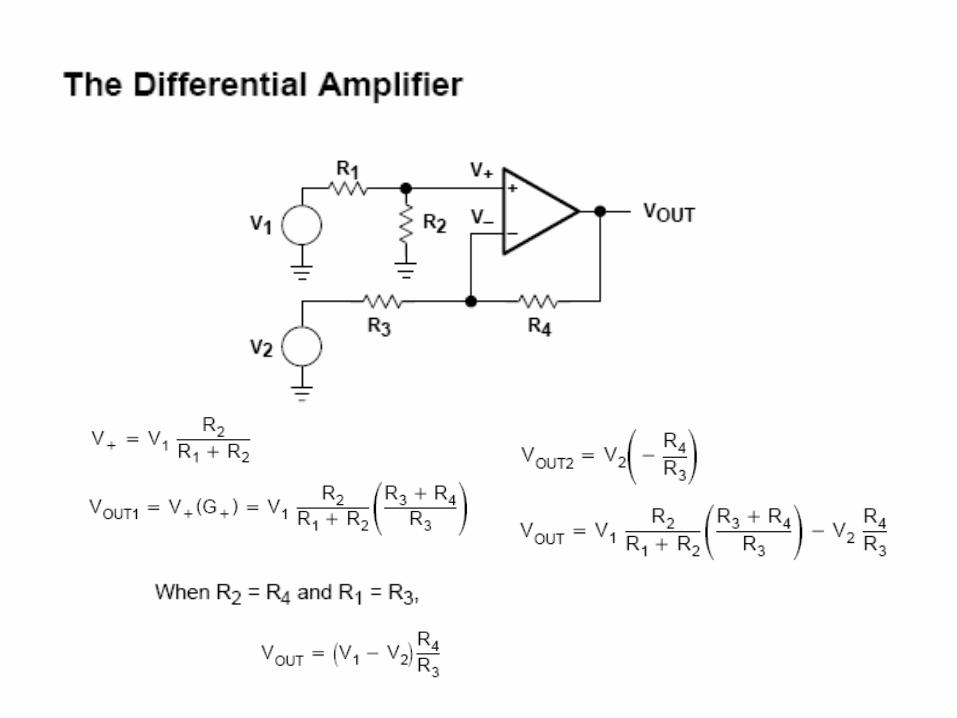
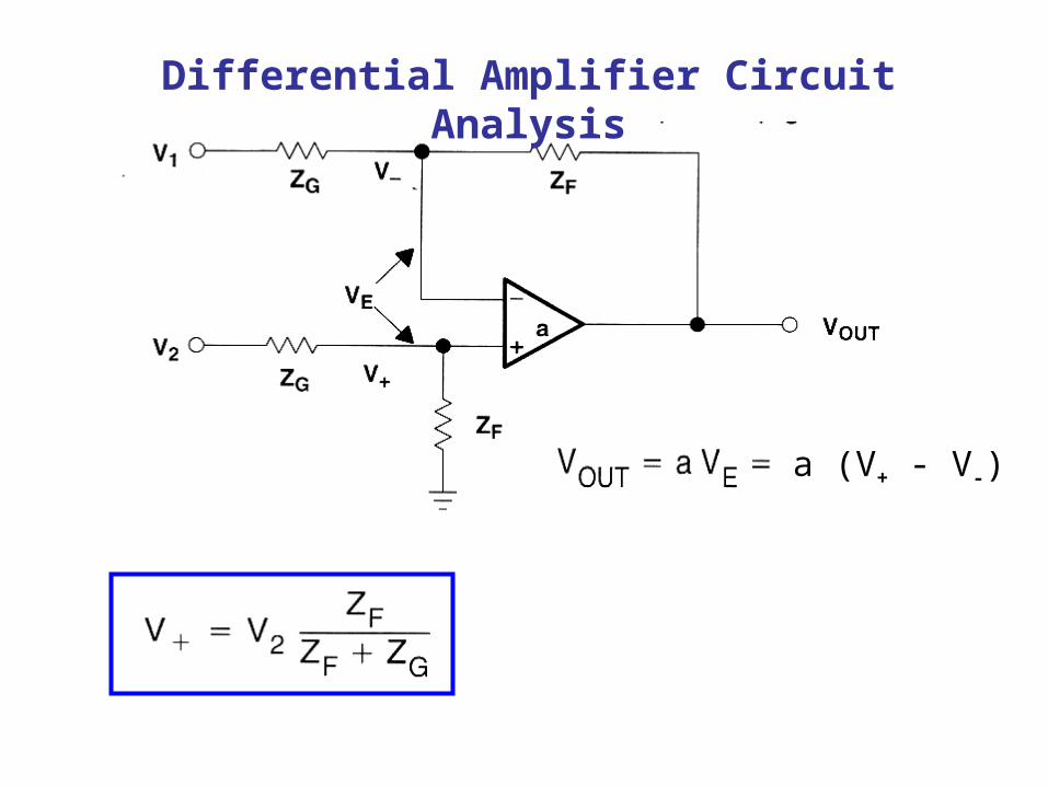
Differential Amplifier Circuit Analysis
a (V+ - V-)
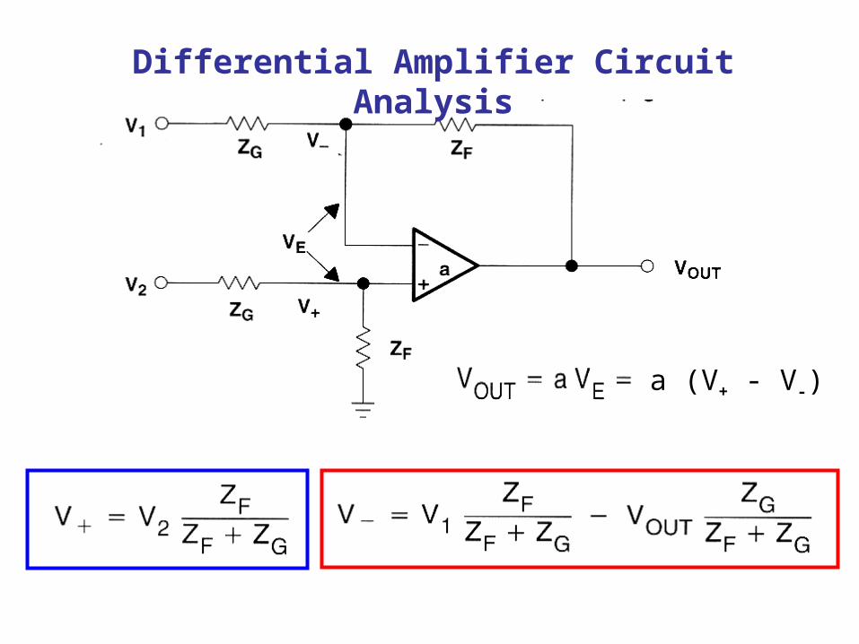
Differential Amplifier Circuit Analysis
a (V+ - V-)
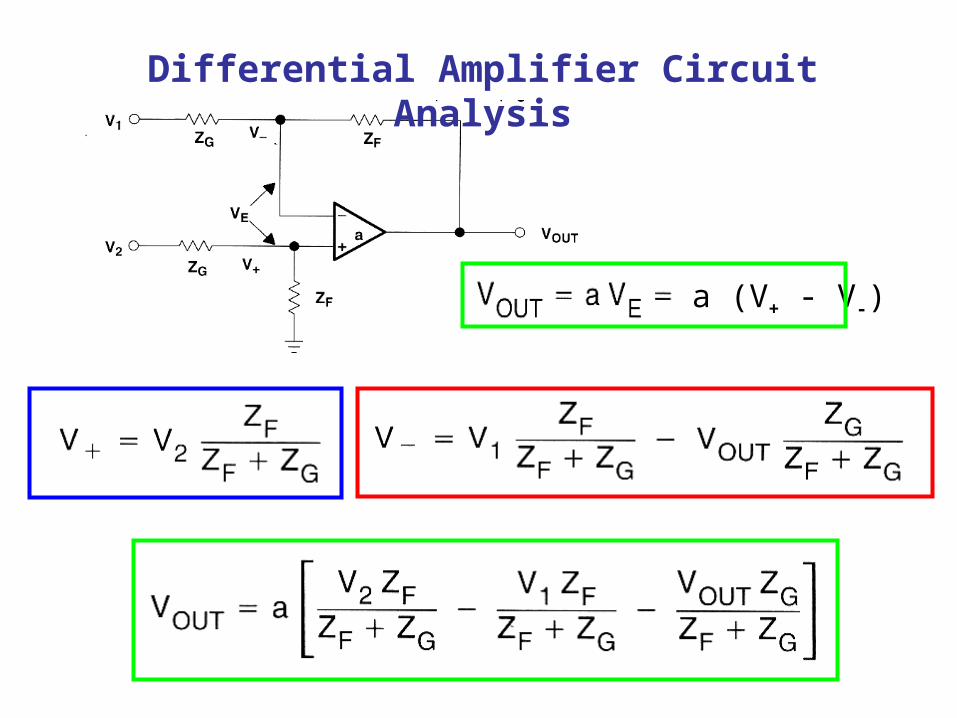
Differential Amplifier Circuit Analysis
a (V+ - V-)
Differential Amplifier Circuit Analysis
a (V+ - V-)

Differential Amplifier Circuit Analysis
a (V+ - V-)
ZF / ZG
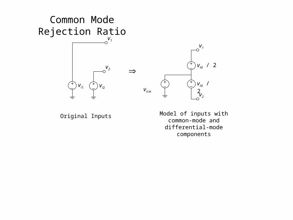
Common Mode Rejection Ratio
vicm
v2
v1
vi1 vi2vid / 2
vid / 2
v2
v1
Original Inputs Model of inputs with common-mode and differential-mode
components
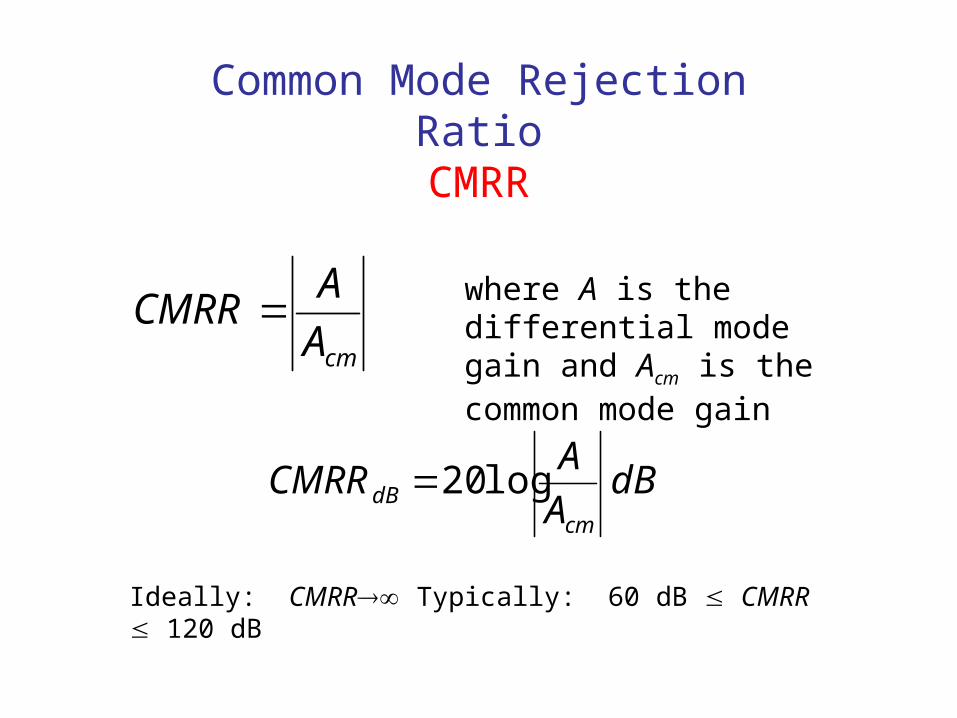
cmA
ACMRR where A is the differential
mode gain and Acm is the common mode gain
dBA
ACMRR
cmdB log20
Ideally: CMRR Typically: 60 dB CMRR 120 dB
Common Mode Rejection RatioCMRR
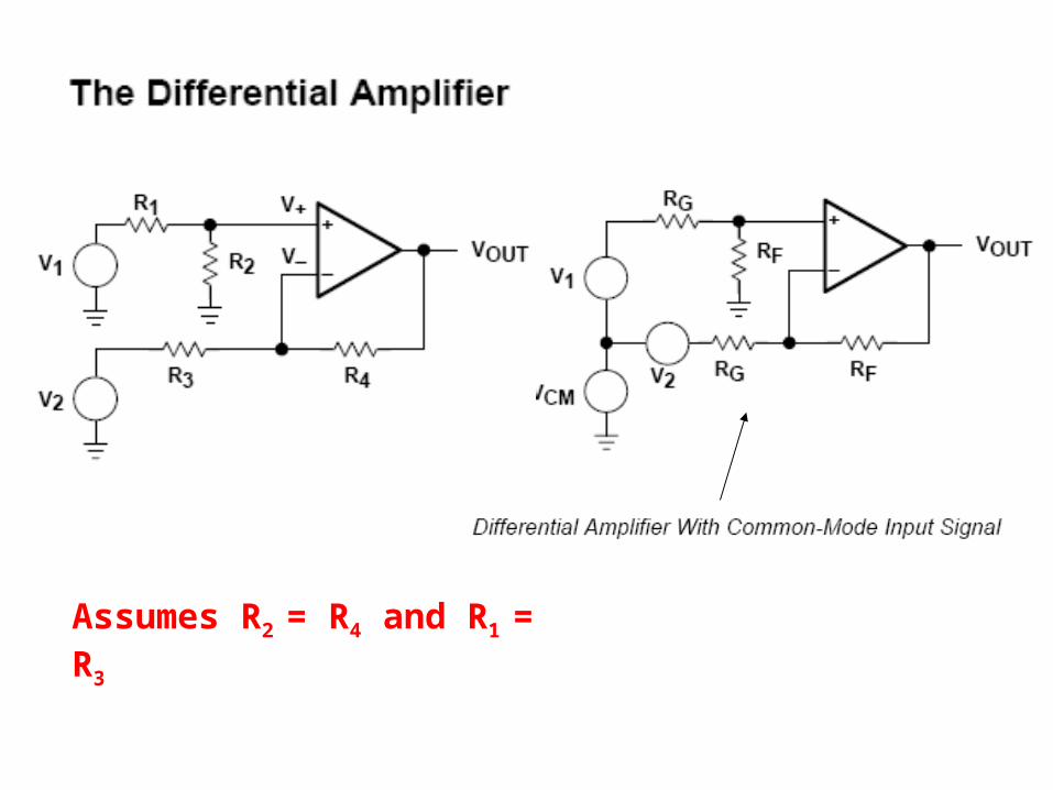
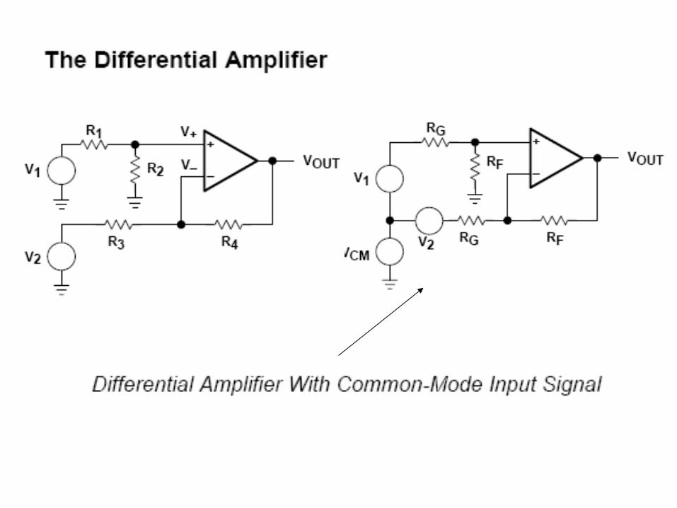
Assumes R2 = R4 and R1 = R3
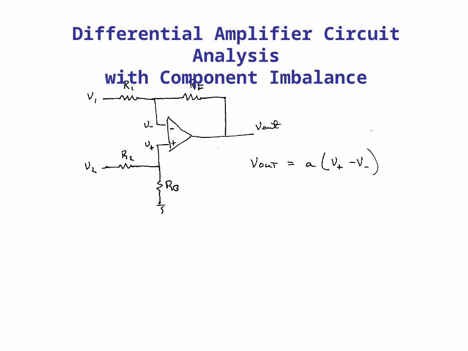
Differential Amplifier Circuit Analysiswith Component Imbalance
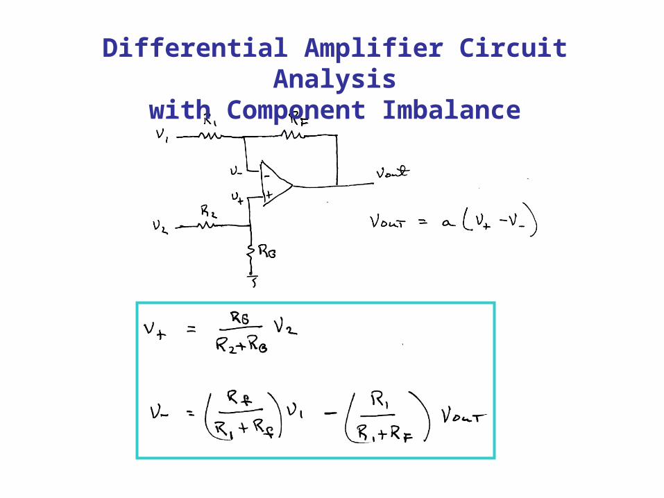
Differential Amplifier Circuit Analysiswith Component Imbalance
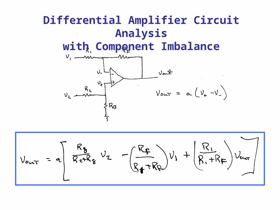
Differential Amplifier Circuit Analysiswith Component Imbalance
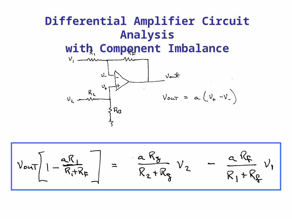
Differential Amplifier Circuit Analysiswith Component Imbalance
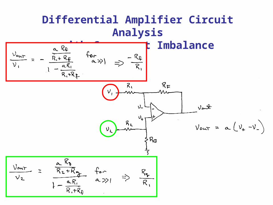
Differential Amplifier Circuit Analysiswith Component Imbalance
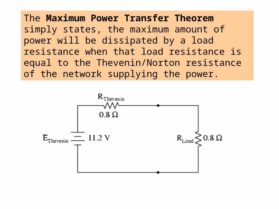
The Maximum Power Transfer Theorem simply states, the maximum amount of power will be dissipated by a load resistance when that load resistance is equal to the Thevenin/Norton resistance of the network supplying the power.
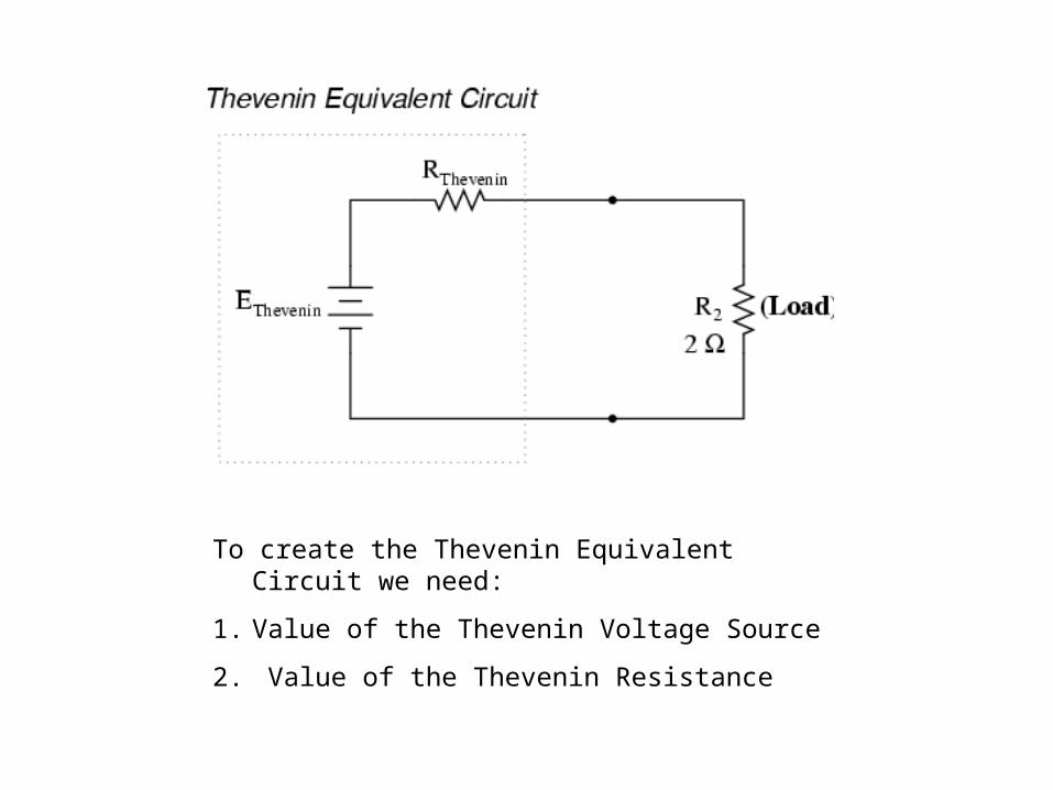
To create the Thevenin Equivalent Circuit we need:
1. Value of the Thevenin Voltage Source
2. Value of the Thevenin Resistance
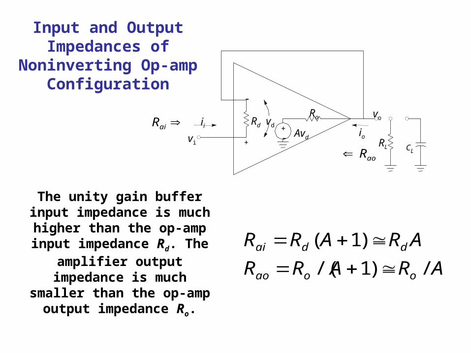
Input and Output Impedances of
Noninverting Op-amp Configuration
The unity gain buffer input impedance is much higher
than the op-amp input impedance Rd. The amplifier output impedance is much smaller than the op-amp
output impedance Ro.
aiR
aoR+
Rdii
Ro
RL CL
ioAvd
vd
vo
vi
+
ARARR
ARARR
ooao
ddai
/)1/(
)1(
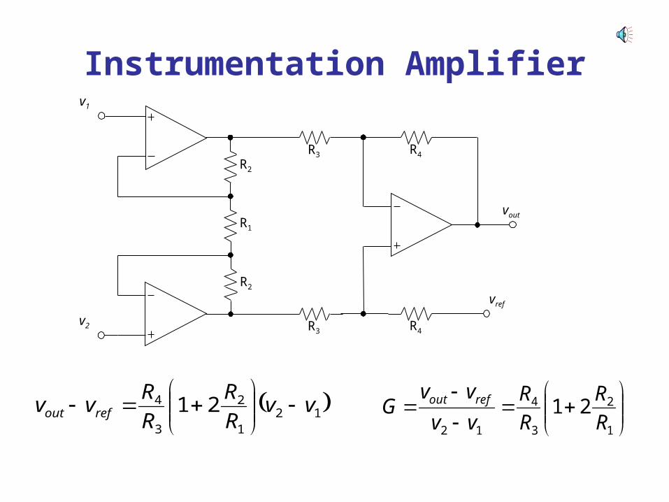
Instrumentation Amplifier
121
2
3
4 21 vvR
R
R
Rvv refout
vout
R3
v1
R2
R3
v2
R1
R2
R4
R4
vref
1
2
3
4
12
21R
R
R
R
vv
vvG refout

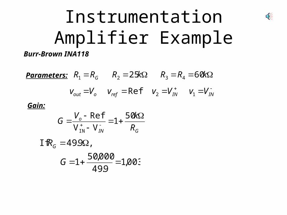
Instrumentation Amplifier Example
Burr-Brown INA118
Parameters: kRRkRRR G 60 25 4321
ININrefoout VvVvvVv 12 Ref
GIN
o
R
kVG
501
VV
Ref
IN
If RG 49.9,
G 1 50,00049.9
1,003
Gain:
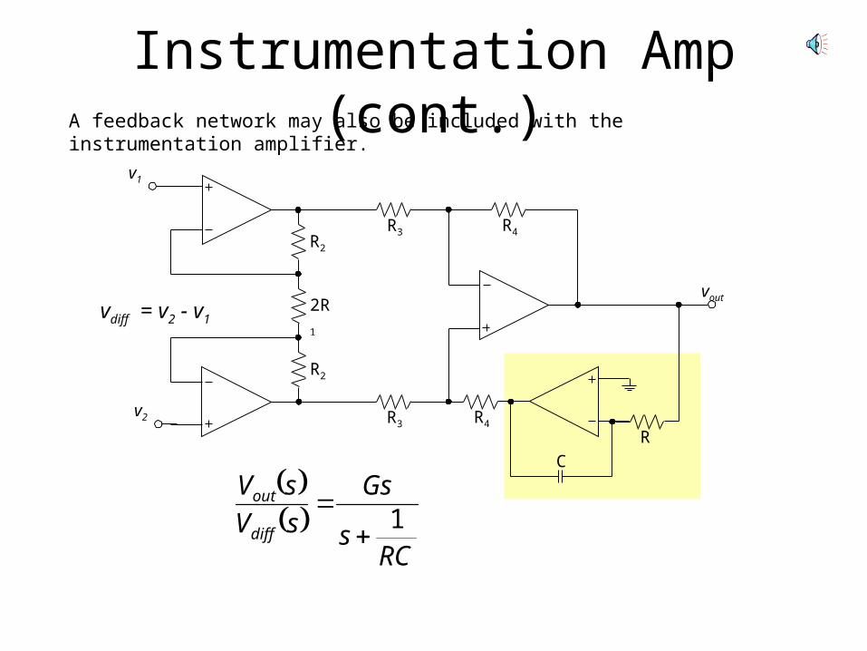
Instrumentation Amp (cont.)A feedback network may also be included with the instrumentation amplifier.
vout
R3
v1
R2
R3
vdiff = v2 - v12R1
R2
R4
R4
R
C
RCs
Gs
sV
sV
diff
out
1
v2